JP7175162B2 - Plasma etching method and plasma etching apparatus for object to be processed - Google Patents
Plasma etching method and plasma etching apparatus for object to be processed Download PDFInfo
- Publication number
- JP7175162B2 JP7175162B2 JP2018208028A JP2018208028A JP7175162B2 JP 7175162 B2 JP7175162 B2 JP 7175162B2 JP 2018208028 A JP2018208028 A JP 2018208028A JP 2018208028 A JP2018208028 A JP 2018208028A JP 7175162 B2 JP7175162 B2 JP 7175162B2
- Authority
- JP
- Japan
- Prior art keywords
- plasma
- processing
- gas
- voltage
- mask
- Prior art date
- Legal status (The legal status is an assumption and is not a legal conclusion. Google has not performed a legal analysis and makes no representation as to the accuracy of the status listed.)
- Active
Links
Images


Classifications
-
- H—ELECTRICITY
- H01—ELECTRIC ELEMENTS
- H01J—ELECTRIC DISCHARGE TUBES OR DISCHARGE LAMPS
- H01J37/00—Discharge tubes with provision for introducing objects or material to be exposed to the discharge, e.g. for the purpose of examination or processing thereof
- H01J37/32—Gas-filled discharge tubes
- H01J37/32431—Constructional details of the reactor
- H01J37/32532—Electrodes
- H01J37/32577—Electrical connecting means
-
- H—ELECTRICITY
- H01—ELECTRIC ELEMENTS
- H01L—SEMICONDUCTOR DEVICES NOT COVERED BY CLASS H10
- H01L21/00—Processes or apparatus adapted for the manufacture or treatment of semiconductor or solid state devices or of parts thereof
- H01L21/02—Manufacture or treatment of semiconductor devices or of parts thereof
- H01L21/04—Manufacture or treatment of semiconductor devices or of parts thereof the devices having at least one potential-jump barrier or surface barrier, e.g. PN junction, depletion layer or carrier concentration layer
- H01L21/18—Manufacture or treatment of semiconductor devices or of parts thereof the devices having at least one potential-jump barrier or surface barrier, e.g. PN junction, depletion layer or carrier concentration layer the devices having semiconductor bodies comprising elements of Group IV of the Periodic System or AIIIBV compounds with or without impurities, e.g. doping materials
- H01L21/30—Treatment of semiconductor bodies using processes or apparatus not provided for in groups H01L21/20 - H01L21/26
- H01L21/302—Treatment of semiconductor bodies using processes or apparatus not provided for in groups H01L21/20 - H01L21/26 to change their surface-physical characteristics or shape, e.g. etching, polishing, cutting
- H01L21/306—Chemical or electrical treatment, e.g. electrolytic etching
- H01L21/3065—Plasma etching; Reactive-ion etching
-
- H—ELECTRICITY
- H01—ELECTRIC ELEMENTS
- H01J—ELECTRIC DISCHARGE TUBES OR DISCHARGE LAMPS
- H01J37/00—Discharge tubes with provision for introducing objects or material to be exposed to the discharge, e.g. for the purpose of examination or processing thereof
- H01J37/02—Details
-
- H—ELECTRICITY
- H01—ELECTRIC ELEMENTS
- H01J—ELECTRIC DISCHARGE TUBES OR DISCHARGE LAMPS
- H01J37/00—Discharge tubes with provision for introducing objects or material to be exposed to the discharge, e.g. for the purpose of examination or processing thereof
- H01J37/02—Details
- H01J37/248—Components associated with high voltage supply
-
- H—ELECTRICITY
- H01—ELECTRIC ELEMENTS
- H01J—ELECTRIC DISCHARGE TUBES OR DISCHARGE LAMPS
- H01J37/00—Discharge tubes with provision for introducing objects or material to be exposed to the discharge, e.g. for the purpose of examination or processing thereof
- H01J37/30—Electron-beam or ion-beam tubes for localised treatment of objects
- H01J37/305—Electron-beam or ion-beam tubes for localised treatment of objects for casting, melting, evaporating or etching
- H01J37/3053—Electron-beam or ion-beam tubes for localised treatment of objects for casting, melting, evaporating or etching for evaporating or etching
-
- H—ELECTRICITY
- H01—ELECTRIC ELEMENTS
- H01J—ELECTRIC DISCHARGE TUBES OR DISCHARGE LAMPS
- H01J37/00—Discharge tubes with provision for introducing objects or material to be exposed to the discharge, e.g. for the purpose of examination or processing thereof
- H01J37/32—Gas-filled discharge tubes
- H01J37/32009—Arrangements for generation of plasma specially adapted for examination or treatment of objects, e.g. plasma sources
- H01J37/32082—Radio frequency generated discharge
- H01J37/32174—Circuits specially adapted for controlling the RF discharge
-
- H—ELECTRICITY
- H01—ELECTRIC ELEMENTS
- H01J—ELECTRIC DISCHARGE TUBES OR DISCHARGE LAMPS
- H01J37/00—Discharge tubes with provision for introducing objects or material to be exposed to the discharge, e.g. for the purpose of examination or processing thereof
- H01J37/32—Gas-filled discharge tubes
- H01J37/32431—Constructional details of the reactor
- H01J37/32623—Mechanical discharge control means
- H01J37/32642—Focus rings
-
- H—ELECTRICITY
- H01—ELECTRIC ELEMENTS
- H01J—ELECTRIC DISCHARGE TUBES OR DISCHARGE LAMPS
- H01J37/00—Discharge tubes with provision for introducing objects or material to be exposed to the discharge, e.g. for the purpose of examination or processing thereof
- H01J37/32—Gas-filled discharge tubes
- H01J37/32431—Constructional details of the reactor
- H01J37/32715—Workpiece holder
-
- H—ELECTRICITY
- H01—ELECTRIC ELEMENTS
- H01J—ELECTRIC DISCHARGE TUBES OR DISCHARGE LAMPS
- H01J37/00—Discharge tubes with provision for introducing objects or material to be exposed to the discharge, e.g. for the purpose of examination or processing thereof
- H01J37/32—Gas-filled discharge tubes
- H01J37/34—Gas-filled discharge tubes operating with cathodic sputtering
- H01J37/3411—Constructional aspects of the reactor
- H01J37/3435—Target holders (includes backing plates and endblocks)
-
- H—ELECTRICITY
- H01—ELECTRIC ELEMENTS
- H01L—SEMICONDUCTOR DEVICES NOT COVERED BY CLASS H10
- H01L21/00—Processes or apparatus adapted for the manufacture or treatment of semiconductor or solid state devices or of parts thereof
- H01L21/02—Manufacture or treatment of semiconductor devices or of parts thereof
- H01L21/02104—Forming layers
- H01L21/02107—Forming insulating materials on a substrate
- H01L21/02109—Forming insulating materials on a substrate characterised by the type of layer, e.g. type of material, porous/non-porous, pre-cursors, mixtures or laminates
- H01L21/02112—Forming insulating materials on a substrate characterised by the type of layer, e.g. type of material, porous/non-porous, pre-cursors, mixtures or laminates characterised by the material of the layer
- H01L21/02123—Forming insulating materials on a substrate characterised by the type of layer, e.g. type of material, porous/non-porous, pre-cursors, mixtures or laminates characterised by the material of the layer the material containing silicon
-
- H—ELECTRICITY
- H01—ELECTRIC ELEMENTS
- H01L—SEMICONDUCTOR DEVICES NOT COVERED BY CLASS H10
- H01L21/00—Processes or apparatus adapted for the manufacture or treatment of semiconductor or solid state devices or of parts thereof
- H01L21/02—Manufacture or treatment of semiconductor devices or of parts thereof
- H01L21/02104—Forming layers
- H01L21/02107—Forming insulating materials on a substrate
- H01L21/02225—Forming insulating materials on a substrate characterised by the process for the formation of the insulating layer
- H01L21/0226—Forming insulating materials on a substrate characterised by the process for the formation of the insulating layer formation by a deposition process
- H01L21/02263—Forming insulating materials on a substrate characterised by the process for the formation of the insulating layer formation by a deposition process deposition from the gas or vapour phase
- H01L21/02266—Forming insulating materials on a substrate characterised by the process for the formation of the insulating layer formation by a deposition process deposition from the gas or vapour phase deposition by physical ablation of a target, e.g. sputtering, reactive sputtering, physical vapour deposition or pulsed laser deposition
-
- H—ELECTRICITY
- H01—ELECTRIC ELEMENTS
- H01L—SEMICONDUCTOR DEVICES NOT COVERED BY CLASS H10
- H01L21/00—Processes or apparatus adapted for the manufacture or treatment of semiconductor or solid state devices or of parts thereof
- H01L21/02—Manufacture or treatment of semiconductor devices or of parts thereof
- H01L21/02104—Forming layers
- H01L21/02107—Forming insulating materials on a substrate
- H01L21/02296—Forming insulating materials on a substrate characterised by the treatment performed before or after the formation of the layer
- H01L21/02299—Forming insulating materials on a substrate characterised by the treatment performed before or after the formation of the layer pre-treatment
- H01L21/02312—Forming insulating materials on a substrate characterised by the treatment performed before or after the formation of the layer pre-treatment treatment by exposure to a gas or vapour
- H01L21/02315—Forming insulating materials on a substrate characterised by the treatment performed before or after the formation of the layer pre-treatment treatment by exposure to a gas or vapour treatment by exposure to a plasma
-
- H—ELECTRICITY
- H01—ELECTRIC ELEMENTS
- H01L—SEMICONDUCTOR DEVICES NOT COVERED BY CLASS H10
- H01L21/00—Processes or apparatus adapted for the manufacture or treatment of semiconductor or solid state devices or of parts thereof
- H01L21/02—Manufacture or treatment of semiconductor devices or of parts thereof
- H01L21/027—Making masks on semiconductor bodies for further photolithographic processing not provided for in group H01L21/18 or H01L21/34
- H01L21/0271—Making masks on semiconductor bodies for further photolithographic processing not provided for in group H01L21/18 or H01L21/34 comprising organic layers
- H01L21/0273—Making masks on semiconductor bodies for further photolithographic processing not provided for in group H01L21/18 or H01L21/34 comprising organic layers characterised by the treatment of photoresist layers
- H01L21/0274—Photolithographic processes
-
- H—ELECTRICITY
- H01—ELECTRIC ELEMENTS
- H01L—SEMICONDUCTOR DEVICES NOT COVERED BY CLASS H10
- H01L21/00—Processes or apparatus adapted for the manufacture or treatment of semiconductor or solid state devices or of parts thereof
- H01L21/02—Manufacture or treatment of semiconductor devices or of parts thereof
- H01L21/04—Manufacture or treatment of semiconductor devices or of parts thereof the devices having at least one potential-jump barrier or surface barrier, e.g. PN junction, depletion layer or carrier concentration layer
- H01L21/18—Manufacture or treatment of semiconductor devices or of parts thereof the devices having at least one potential-jump barrier or surface barrier, e.g. PN junction, depletion layer or carrier concentration layer the devices having semiconductor bodies comprising elements of Group IV of the Periodic System or AIIIBV compounds with or without impurities, e.g. doping materials
- H01L21/30—Treatment of semiconductor bodies using processes or apparatus not provided for in groups H01L21/20 - H01L21/26
- H01L21/31—Treatment of semiconductor bodies using processes or apparatus not provided for in groups H01L21/20 - H01L21/26 to form insulating layers thereon, e.g. for masking or by using photolithographic techniques; After treatment of these layers; Selection of materials for these layers
- H01L21/3105—After-treatment
- H01L21/311—Etching the insulating layers by chemical or physical means
- H01L21/31105—Etching inorganic layers
- H01L21/31111—Etching inorganic layers by chemical means
- H01L21/31116—Etching inorganic layers by chemical means by dry-etching
-
- H—ELECTRICITY
- H01—ELECTRIC ELEMENTS
- H01L—SEMICONDUCTOR DEVICES NOT COVERED BY CLASS H10
- H01L21/00—Processes or apparatus adapted for the manufacture or treatment of semiconductor or solid state devices or of parts thereof
- H01L21/02—Manufacture or treatment of semiconductor devices or of parts thereof
- H01L21/04—Manufacture or treatment of semiconductor devices or of parts thereof the devices having at least one potential-jump barrier or surface barrier, e.g. PN junction, depletion layer or carrier concentration layer
- H01L21/18—Manufacture or treatment of semiconductor devices or of parts thereof the devices having at least one potential-jump barrier or surface barrier, e.g. PN junction, depletion layer or carrier concentration layer the devices having semiconductor bodies comprising elements of Group IV of the Periodic System or AIIIBV compounds with or without impurities, e.g. doping materials
- H01L21/30—Treatment of semiconductor bodies using processes or apparatus not provided for in groups H01L21/20 - H01L21/26
- H01L21/31—Treatment of semiconductor bodies using processes or apparatus not provided for in groups H01L21/20 - H01L21/26 to form insulating layers thereon, e.g. for masking or by using photolithographic techniques; After treatment of these layers; Selection of materials for these layers
- H01L21/3105—After-treatment
- H01L21/311—Etching the insulating layers by chemical or physical means
- H01L21/31127—Etching organic layers
- H01L21/31133—Etching organic layers by chemical means
- H01L21/31138—Etching organic layers by chemical means by dry-etching
-
- H—ELECTRICITY
- H01—ELECTRIC ELEMENTS
- H01L—SEMICONDUCTOR DEVICES NOT COVERED BY CLASS H10
- H01L21/00—Processes or apparatus adapted for the manufacture or treatment of semiconductor or solid state devices or of parts thereof
- H01L21/02—Manufacture or treatment of semiconductor devices or of parts thereof
- H01L21/04—Manufacture or treatment of semiconductor devices or of parts thereof the devices having at least one potential-jump barrier or surface barrier, e.g. PN junction, depletion layer or carrier concentration layer
- H01L21/18—Manufacture or treatment of semiconductor devices or of parts thereof the devices having at least one potential-jump barrier or surface barrier, e.g. PN junction, depletion layer or carrier concentration layer the devices having semiconductor bodies comprising elements of Group IV of the Periodic System or AIIIBV compounds with or without impurities, e.g. doping materials
- H01L21/30—Treatment of semiconductor bodies using processes or apparatus not provided for in groups H01L21/20 - H01L21/26
- H01L21/31—Treatment of semiconductor bodies using processes or apparatus not provided for in groups H01L21/20 - H01L21/26 to form insulating layers thereon, e.g. for masking or by using photolithographic techniques; After treatment of these layers; Selection of materials for these layers
- H01L21/3105—After-treatment
- H01L21/311—Etching the insulating layers by chemical or physical means
- H01L21/31144—Etching the insulating layers by chemical or physical means using masks
-
- H—ELECTRICITY
- H01—ELECTRIC ELEMENTS
- H01L—SEMICONDUCTOR DEVICES NOT COVERED BY CLASS H10
- H01L21/00—Processes or apparatus adapted for the manufacture or treatment of semiconductor or solid state devices or of parts thereof
- H01L21/02—Manufacture or treatment of semiconductor devices or of parts thereof
- H01L21/04—Manufacture or treatment of semiconductor devices or of parts thereof the devices having at least one potential-jump barrier or surface barrier, e.g. PN junction, depletion layer or carrier concentration layer
- H01L21/18—Manufacture or treatment of semiconductor devices or of parts thereof the devices having at least one potential-jump barrier or surface barrier, e.g. PN junction, depletion layer or carrier concentration layer the devices having semiconductor bodies comprising elements of Group IV of the Periodic System or AIIIBV compounds with or without impurities, e.g. doping materials
- H01L21/30—Treatment of semiconductor bodies using processes or apparatus not provided for in groups H01L21/20 - H01L21/26
- H01L21/31—Treatment of semiconductor bodies using processes or apparatus not provided for in groups H01L21/20 - H01L21/26 to form insulating layers thereon, e.g. for masking or by using photolithographic techniques; After treatment of these layers; Selection of materials for these layers
- H01L21/3205—Deposition of non-insulating-, e.g. conductive- or resistive-, layers on insulating layers; After-treatment of these layers
- H01L21/32055—Deposition of semiconductive layers, e.g. poly - or amorphous silicon layers
-
- H—ELECTRICITY
- H01—ELECTRIC ELEMENTS
- H01L—SEMICONDUCTOR DEVICES NOT COVERED BY CLASS H10
- H01L21/00—Processes or apparatus adapted for the manufacture or treatment of semiconductor or solid state devices or of parts thereof
- H01L21/67—Apparatus specially adapted for handling semiconductor or electric solid state devices during manufacture or treatment thereof; Apparatus specially adapted for handling wafers during manufacture or treatment of semiconductor or electric solid state devices or components ; Apparatus not specifically provided for elsewhere
- H01L21/67005—Apparatus not specifically provided for elsewhere
- H01L21/67011—Apparatus for manufacture or treatment
- H01L21/67017—Apparatus for fluid treatment
- H01L21/67063—Apparatus for fluid treatment for etching
- H01L21/67069—Apparatus for fluid treatment for etching for drying etching
-
- H—ELECTRICITY
- H01—ELECTRIC ELEMENTS
- H01L—SEMICONDUCTOR DEVICES NOT COVERED BY CLASS H10
- H01L21/00—Processes or apparatus adapted for the manufacture or treatment of semiconductor or solid state devices or of parts thereof
- H01L21/67—Apparatus specially adapted for handling semiconductor or electric solid state devices during manufacture or treatment thereof; Apparatus specially adapted for handling wafers during manufacture or treatment of semiconductor or electric solid state devices or components ; Apparatus not specifically provided for elsewhere
- H01L21/67005—Apparatus not specifically provided for elsewhere
- H01L21/67242—Apparatus for monitoring, sorting or marking
- H01L21/67253—Process monitoring, e.g. flow or thickness monitoring
-
- H—ELECTRICITY
- H01—ELECTRIC ELEMENTS
- H01L—SEMICONDUCTOR DEVICES NOT COVERED BY CLASS H10
- H01L21/00—Processes or apparatus adapted for the manufacture or treatment of semiconductor or solid state devices or of parts thereof
- H01L21/67—Apparatus specially adapted for handling semiconductor or electric solid state devices during manufacture or treatment thereof; Apparatus specially adapted for handling wafers during manufacture or treatment of semiconductor or electric solid state devices or components ; Apparatus not specifically provided for elsewhere
- H01L21/683—Apparatus specially adapted for handling semiconductor or electric solid state devices during manufacture or treatment thereof; Apparatus specially adapted for handling wafers during manufacture or treatment of semiconductor or electric solid state devices or components ; Apparatus not specifically provided for elsewhere for supporting or gripping
- H01L21/6831—Apparatus specially adapted for handling semiconductor or electric solid state devices during manufacture or treatment thereof; Apparatus specially adapted for handling wafers during manufacture or treatment of semiconductor or electric solid state devices or components ; Apparatus not specifically provided for elsewhere for supporting or gripping using electrostatic chucks
-
- H—ELECTRICITY
- H01—ELECTRIC ELEMENTS
- H01L—SEMICONDUCTOR DEVICES NOT COVERED BY CLASS H10
- H01L21/00—Processes or apparatus adapted for the manufacture or treatment of semiconductor or solid state devices or of parts thereof
- H01L21/67—Apparatus specially adapted for handling semiconductor or electric solid state devices during manufacture or treatment thereof; Apparatus specially adapted for handling wafers during manufacture or treatment of semiconductor or electric solid state devices or components ; Apparatus not specifically provided for elsewhere
- H01L21/683—Apparatus specially adapted for handling semiconductor or electric solid state devices during manufacture or treatment thereof; Apparatus specially adapted for handling wafers during manufacture or treatment of semiconductor or electric solid state devices or components ; Apparatus not specifically provided for elsewhere for supporting or gripping
- H01L21/687—Apparatus specially adapted for handling semiconductor or electric solid state devices during manufacture or treatment thereof; Apparatus specially adapted for handling wafers during manufacture or treatment of semiconductor or electric solid state devices or components ; Apparatus not specifically provided for elsewhere for supporting or gripping using mechanical means, e.g. chucks, clamps or pinches
- H01L21/68714—Apparatus specially adapted for handling semiconductor or electric solid state devices during manufacture or treatment thereof; Apparatus specially adapted for handling wafers during manufacture or treatment of semiconductor or electric solid state devices or components ; Apparatus not specifically provided for elsewhere for supporting or gripping using mechanical means, e.g. chucks, clamps or pinches the wafers being placed on a susceptor, stage or support
- H01L21/68735—Apparatus specially adapted for handling semiconductor or electric solid state devices during manufacture or treatment thereof; Apparatus specially adapted for handling wafers during manufacture or treatment of semiconductor or electric solid state devices or components ; Apparatus not specifically provided for elsewhere for supporting or gripping using mechanical means, e.g. chucks, clamps or pinches the wafers being placed on a susceptor, stage or support characterised by edge profile or support profile
-
- H—ELECTRICITY
- H01—ELECTRIC ELEMENTS
- H01J—ELECTRIC DISCHARGE TUBES OR DISCHARGE LAMPS
- H01J2237/00—Discharge tubes exposing object to beam, e.g. for analysis treatment, etching, imaging
- H01J2237/32—Processing objects by plasma generation
- H01J2237/33—Processing objects by plasma generation characterised by the type of processing
- H01J2237/334—Etching
- H01J2237/3341—Reactive etching
Description
本開示は、被処理体のプラズマエッチング方法及びプラズマエッチング装置に関する。
The present disclosure relates to a plasma etching method and a plasma etching apparatus for an object to be processed.
特許文献1には、シャワーヘッドに直流負電圧を印加しながら、フォトレジスト層をマスクに用いて、有機膜を、エッチングする被処理体の処理方法が開示されている。
一の側面では、本開示は、被処理体のマスクを処理する被処理体のプラズマエッチング方法及びプラズマエッチング装置を提供する。
In one aspect, the present disclosure provides a plasma etching method and plasma etching apparatus for processing a mask of an object to be processed.
上記課題を解決するために、一の態様によれば、処理容器と、前記処理容器内において被処理体を載置する載置台と、前記載置台の周囲に配置される外周部材と、前記外周部材に電圧を印加する第1電圧印加装置と、前記載置台に対向する上部電極と、前記上部電極に電圧を印加する第2電圧印加装置と、下部電極としての前記載置台に高周波電力を印加して前記下部電極と前記上部電極との間に容量結合プラズマを生成する高周波電源と、を備えるプラズマエッチング装置を用いて、被処理体を処理する被処理体のプラズマエッチング方法であって、被エッチング膜と、前記被エッチング膜上に形成されたパターン化されたマスクと、を有する前記被処理体を準備する工程と、前記マスクを処理する工程と、前記マスクを処理する工程の後、前記被エッチング膜をエッチングするエッチング工程と、を含み、前記マスクを処理する工程は、第1の希ガスを含む第1の処理ガスを前記処理容器に供給する工程と、前記外周部材に直流電圧を印加しながら、前記被処理体の外周部に位置する前記マスクを前記第1の処理ガスのプラズマにより処理する第1のプラズマ処理工程と、第2の希ガスを含む第2の処理ガスを前記処理容器に供給する工程と、前記上部電極に直流電圧を印加しながら、前記被処理体の中心部および外周部に位置する前記マスクを前記第2の処理ガスのプラズマにより処理する第2のプラズマ処理工程と、を含み、前記マスクを処理する工程において、前記第2のプラズマ処理工程が実行され、前記第2のプラズマ処理工程が実行された後に、前記第1のプラズマ処理工程が実行され、前記エッチング工程は、第3の処理ガスを前記処理容器に供給する工程と、前記第3の処理ガスのプラズマにより処理する工程と、を含む、被処理体のプラズマエッチング方法が提供される。
In order to solve the above problems, according to one aspect, there is provided a processing container, a mounting table for mounting an object to be processed in the processing container, an outer peripheral member arranged around the mounting table, and the outer peripheral member. A first voltage applying device that applies a voltage to a member, an upper electrode that faces the mounting table, a second voltage applying device that applies a voltage to the upper electrode, and a high frequency power is applied to the mounting table as a lower electrode. and a high-frequency power source for generating capacitively coupled plasma between the lower electrode and the upper electrode. preparing the object to be processed having an etching film and a patterned mask formed on the film to be etched; treating the mask; and after treating the mask, an etching step of etching a film to be etched , wherein the step of treating the mask comprises supplying a first processing gas containing a first rare gas to the processing container; and applying a DC voltage to the peripheral member. a first plasma processing step of processing the mask positioned on the outer peripheral portion of the object to be processed with plasma of the first processing gas while applying a second processing gas containing a second rare gas; a step of supplying a second plasma to a processing chamber; and applying a DC voltage to the upper electrode to process the mask positioned at the central portion and the outer peripheral portion of the object to be processed with the plasma of the second processing gas. and, in the step of treating the mask, the second plasma treatment step is performed, and after the second plasma treatment step is performed, the first plasma treatment step is performed. A plasma etching method for an object to be processed is provided , wherein the etching step includes a step of supplying a third processing gas to the processing container, and a step of processing with plasma of the third processing gas .
一の側面によれば、被処理体のマスクを処理する被処理体のプラズマエッチング方法及びプラズマエッチング装置を提供することができる。
According to one aspect, it is possible to provide a plasma etching method and a plasma etching apparatus for processing a mask of an object to be processed.
以下、図面を参照して本開示を実施するための形態について説明する。各図面において、同一構成部分には同一符号を付し、重複した説明を省略する場合がある。 Hereinafter, embodiments for carrying out the present disclosure will be described with reference to the drawings. In each drawing, the same components are denoted by the same reference numerals, and redundant description may be omitted.
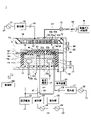
<基板処理装置>
図1は、一実施形態に係る基板処理装置1の一例を示す図である。一実施形態に係る基板処理装置1は、容量結合型の平行平板処理装置であり、例えば表面が陽極酸化処理されたアルミニウムからなる円筒状の処理容器10を有している。処理容器10は接地されている。
<Substrate processing equipment>
FIG. 1 is a diagram showing an example of a
処理容器10の底部には、セラミックス等からなる絶縁板12を介して円柱状の支持台14が配置され、この支持台14の上に例えばアルミニウムからなる載置台16が設けられている。載置台16は、静電チャック20と基台16aとエッジリング24とインシュレータリング26とを有する。静電チャック20は、基板の一例であるウェハWを載置する。静電チャック20は、導電膜からなる第1の電極20aを絶縁層20bで挟んだ構造を有し、第1の電極20aには直流電源22が接続されている。静電チャック20は、ヒータを有し、温度制御が可能であってもよい。
A cylindrical support table 14 is arranged at the bottom of the
ウェハWの周囲には、例えばシリコンからなる導電性のエッジリング24が配置されている。エッジリング24は、フォーカスリングとも呼ぶ。静電チャック20、基台16a及び支持台14の周囲には、例えば石英からなる環状のインシュレータリング26が設けられている。
Around the wafer W is arranged a
静電チャック20のエッジリング24と対向する位置には、第2の電極21が埋め込まれている。第2の電極21には、直流電源23が接続されている。直流電源22および直流電源23は、それぞれ個別に直流電圧を印加する。静電チャック20の中央部は、直流電源22から第1の電極20aに印加された電圧によりクーロン力等の静電力を発生させ、静電力により静電チャック20にウェハWを吸着保持する。また、静電チャック20の周辺部は、直流電源23から第2の電極21に印加された電圧によりクーロン力等の静電力を発生させ、静電力により静電チャック20にエッジリング24を吸着保持する。
A
支持台14の内部には、例えば円周上に冷媒室28が設けられている。冷媒室28には、外部に設けられたチラーユニットより配管30a,30bを介して所定温度の冷媒、例えば冷却水が循環供給され、冷媒の温度によって載置台16上のウェハWの温度が制御される。さらに、伝熱ガス供給機構からの伝熱ガス、例えばHeガスがガス供給ライン32を介して静電チャック20の上面とウェハWの裏面との間に供給される。
A
載置台16の上方には、載置台16と対向して上部電極34が設けられている。上部電極34と載置台16の間はプラズマ処理空間となる。
An
上部電極34は、絶縁性の遮蔽部材42を介して処理容器10の天井部の開口を閉塞するように設けられる。上部電極34は、載置台16との対向面を構成し、かつ多数のガス吐出孔37を有する電極板36と、この電極板36を着脱自在に支持し、導電性材料、例えば表面が陽極酸化処理されたアルミニウムからなる電極支持体38とを有する。電極板36は、シリコンやSiC等のシリコン含有物で構成される。電極支持体38の内部には、ガス拡散室40a、40bが設けられ、このガス拡散室40a、40bからはガス吐出孔37に連通する多数のガス通流孔41a、41bが下方に延びている。
The
電極支持体38には、ガス拡散室40a、40bへガスを導くガス導入口62が形成されており、このガス導入口62にはガス供給管64が接続され、ガス供給管64には処理ガス供給源66が接続されている。ガス供給管64には、処理ガス供給源66が配置された上流側から順にマスフローコントローラ(MFC)68および開閉バルブ70が設けられている。そして、処理ガス供給源66から、処理ガスがガス供給管64を介してガス拡散室40a、40b、ガス通流孔41a、41bを通り、ガス吐出孔37からシャワー状に吐出される。
The
載置台16には、給電棒89及び整合器88を介して第1の高周波電源90が接続されている。第1の高周波電源90は、HF(High Frequency)電力を載置台16に印加する。整合器88は、第1の高周波電源90の内部インピーダンスと負荷インピーダンスとを整合させる。これにより、プラズマ処理空間においてガスからプラズマが生成される。なお、第1の高周波電源90から供給されるHF電力を、上部電極34に印加してもよい。HF電力を載置台16に印加する場合、HFの周波数は、13MHz~100MHzの範囲であればよく、例えば40MHzであってもよい。
A first high-
載置台16には、給電棒47及び整合器46を介して第2の高周波電源48が接続されている。第2の高周波電源48は、LF(Low Frequency)電力を載置台16に印加する。整合器46は、第2の高周波電源48の内部インピーダンスと負荷インピーダンスとを整合させる。これにより、載置台16上のウェハWにイオンが引き込まれる。第2の高周波電源48は、400kHz~13.56MHzの範囲内の周波数の高周波電力を出力する。載置台16には、所定の高周波をグランドに通すためのフィルタが接続されてもよい。
A second high-
LFの周波数はHFの周波数よりも低い。LF及びHFの電圧又は電流は、連続波であってもよく、パルス波であってもよい。このように、ガスを供給するシャワーヘッドは、上部電極34として機能し、載置台16は下部電極として機能する。
The frequency of LF is lower than that of HF. The LF and HF voltages or currents may be continuous waves or pulse waves. Thus, the showerhead that supplies gas functions as the
上部電極34には、可変直流電源50が接続され、可変直流電源50からの直流電圧が上部電極34に印加される。また、エッジリング24には、可変直流電源55が接続され、可変直流電源55からの直流電圧がエッジリング24に印加される。なお、可変直流電源55は第1電圧印加装置に相当し、可変直流電源50は第2電圧印加装置に相当する。
A variable
図7は、他の実施形態に係る基板処理装置1の一例を示す図である。図7に示す基板処理装置1は、図1に示す基板処理装置1と比較して、第1電圧印加装置及び第2電圧印加装置の構成が異なっている。その他の構成は図1に示す基板処理装置1と同様であり、重複する説明を省略する。
FIG. 7 is a diagram showing an example of a
図7に示すように、上部電極34には、可変直流電源50の代わりに整合器52、ブロッキングコンデンサ53を介して交流電源51が接続されてもよい。また、エッジリング24には、可変直流電源55の代わりに整合器57、ブロッキングコンデンサ58を介して交流電源56が接続されてもよい。なお、この場合、交流電源56は第1電圧印加装置に相当し、交流電源51は第2電圧印加装置に相当する。
As shown in FIG. 7 , an
交流電源51および交流電源56は、プラズマ中のイオンが追従できる周波数fを有する交流、つまりイオンプラズマ周波数よりも低い低周波または高周波の交流ACを出力し、そのパワー、電圧波高値または実効値を可変できるようになっている。
The
エッチングプロセス中に交流電源51からの交流ACがブロッキングコンデンサ53を介して上部電極34に印加されると、上部電極34には自己バイアス電圧VBが発生する。即ち、上部電極34に負の直流電圧成分が印加され、この負の直流電圧成分に交流ACの電圧(瞬時値)が重畳される。同様に、交流電源56からの交流ACがブロッキングコンデンサ58を介してエッジリング24に印加されると、エッジリング24にも負の直流電圧成分が印加されたことになる。
When alternating current AC from alternating
ここで、交流ACの周波数fがイオンプラズマ周波数fpiよりも低く、上部電極34付近もしくはエッジリング24の電子温度は低いので、自己バイアス電圧VBは交流ACの電圧波高値に近い値になる。こうして、上部電極34もしくはエッジリング24の電位は、自己バイアス電圧VBに交流ACの電圧レベル(瞬時値)が重なって周期的に変化する。
Here, since the frequency f of the alternating AC is lower than the ion plasma frequency fpi and the electron temperature near the
図1に戻り、チャンバ10内で処理空間に面する適当な箇所として例えば上部電極34の半径方向外側あるいはインシュレータリング26の頂部付近に、例えばSi,SiC等の導電性部材からなるリング状のDCグランドパーツ(図示せず)が取り付けられている。このDCグランドパーツは、接地ライン(図示せず)を介して常時接地されている。プラズマエッチング中に第2電圧印加装置によって上部電極34に直流電圧が印加されると上部電極34とDCグランドパーツとの間でプラズマを介して直流の電子電流が流れるようになっている。また、第1電圧印加装置によってエッジリング24に直流電圧が印加されるとエッジリング24とDCグランドパーツとの間でプラズマを介して直流の電子電流が流れるようになっている。
Returning to FIG. 1, a ring-shaped DC electrode made of a conductive material such as Si or SiC is placed, for example, in the radially outer side of the
処理容器10の底部には排気口80が設けられ、この排気口80に排気管82を介して排気装置84が接続されている。排気装置84は、ターボ分子ポンプなどの真空ポンプを有しており、処理容器10内を所望の真空度まで減圧する。また、処理容器10の側壁にはウェハWの搬入出口85が設けられており、この搬入出口85はゲートバルブ86により開閉可能である。
An
環状のインシュレータリング26と処理容器10の側壁との間には、環状のバッフル板83が設けられている。バッフル板83には、アルミニウム材にY2O3等のセラミックスを被覆したものを用いることができる。
An
かかる構成の基板処理装置1においてエッチング処理等の所定の処理を行う際には、まず、ゲートバルブ86を開状態とし、搬入出口85を介してウェハWを処理容器10内に搬入し、載置台16の上に載置する。そして、処理ガス供給源66からエッチング等の所定の処理のためのガスを所定の流量でガス拡散室40a、40bへ供給し、ガス通流孔41a、41bおよびガス吐出孔37を介して処理容器10内へ供給する。また、排気装置84により処理容器10内を排気する。これにより、内部の圧力は例えば0.1~150Paの範囲内の設定値に制御される。
When performing a predetermined process such as an etching process in the
このように処理容器10内に所定のガスを導入した状態で、第1の高周波電源90からHF電力を載置台16に印加する。また、第2の高周波電源48からLF電力を載置台16に印加する。また、直流電源22から直流電圧を第1の電極20aに印加し、ウェハWを載置台16に保持する。また、直流電源23から直流電圧を第2の電極21に印加し、エッジリング24を載置台16に保持する。また、可変直流電源50から直流電圧を上部電極34に印加してもよい。また、可変直流電源55から直流電圧を載置台16に印加してもよい。
HF power is applied to the mounting table 16 from the first high-
上部電極34のガス吐出孔37から吐出されたガスは、主にHFの高周波電力により解離及び電離しプラズマとなり、プラズマ中のラジカルやイオンによってウェハWの被処理面にエッチング等の処理が施される。また、載置台16にLFの高周波電力を印加することで、プラズマ中のイオンを制御し、エッチング等の処理が促進される。
The gas discharged from the gas discharge holes 37 of the
基板処理装置1には、装置全体の動作を制御する制御部200が設けられている。制御部200に設けられたCPUは、ROM及びRAM等のメモリに格納されたレシピに従って、エッチング等の所望のプラズマ処理を実行する。レシピには、プロセス条件に対する装置の制御情報であるプロセス時間、圧力(ガスの排気)、HFの高周波電力(以下、HF電力ともいう。)及びLFの高周波電力(以下、LF電力ともいう。)や電圧、各種ガス流量が設定されてもよい。また、レシピには、処理容器内温度(上部電極温度、処理容器の側壁温度、ウェハW温度、静電チャック温度等)、チラーから出力される冷媒の温度などが設定されてもよい。なお、これらのプログラムや処理条件を示すレシピは、ハードディスクや半導体メモリに記憶されてもよい。また、レシピは、CD-ROM、DVD等の可搬性のコンピュータにより読み取り可能な記憶媒体に収容された状態で所定位置にセットされ、読み出されるようにしてもよい。
The
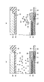
次に、図2及び図3を用いて、フォトレジスト層の改質処理について説明する。図2は、一実施形態に係る基板処理装置1における希ガスイオンとスパッタされたシリコンの移動の一例を示す図であり、(a)は上部電極34に直流負電圧を印加した場合を示し、(b)はエッジリング24に直流負電圧を印加した場合を示す。
Next, the modification process of the photoresist layer will be described with reference to FIGS. 2 and 3. FIG. FIG. 2 is a diagram showing an example of movement of rare gas ions and sputtered silicon in the
フォトレジスト層の改質処理において、処理ガス供給源66から希ガスを含む処理ガスがプラズマ処理空間に供給される。希ガスとしては、例えば、アルゴン、ヘリウム、クリプトン、キセノン等を用いることができる。また、処理ガスは、希ガスのみであってもよい。また、水素を含むガスと希ガスとを含む混合ガスであってもよい。水素を含むガスとしては、例えば、H2、CH4、CH3F、HBr等を用いることができる。なお、以下の説明において、処理ガスは、H2とArの混合ガスである場合を例に説明する。
In the modification process of the photoresist layer, a processing gas containing a rare gas is supplied from the processing
プラズマ処理空間に供給されたH2ガス及びArガスは、主にHF電力により解離及び電離してプラズマとなる。プラズマ中には、水素ラジカル(H* )及びアルゴンイオン(Ar+ )が含まれる。 The H 2 gas and Ar gas supplied to the plasma processing space are dissociated and ionized mainly by HF power to become plasma. The plasma contains hydrogen radicals (H * ) and argon ions (Ar + ).
ここで、図2(a)に示すように、エッジリング24に電圧を印加していない状態で上部電極34に直流負電圧を印加すると、アルゴンイオン101は、矢印A1に示すように上部電極34へ向かって移動し、シリコンまたはSiCで構成される上部電極34へ衝突する。これにより、上部電極34のシリコンがスパッタされ、シリコン102がプラズマ処理空間に放出される。同時に、プラズマ処理空間に電子が放出される。シリコン102は、矢印A2に示すように降下する。これにより、ウェハW上にシリコン102が堆積する。ここで、上部電極34は、ウェハW全体を覆うように配置されている。また、上部電極34からウェハWまでのプラズマ処理空間内でシリコン102が拡散しながら降下する。このため、シリコン102は、ウェハWの全体(ウェハWの中心部及び外周部)に堆積する。
Here, as shown in FIG. 2(a), when a DC negative voltage is applied to the
また、図2(b)に示すように、上部電極34に電圧を印加していない状態でエッジリング24に直流負電圧を印加すると、アルゴンイオン101は、矢印A3に示すようにエッジリング24へ向かって移動し、シリコンまたはSiCで構成されるエッジリング24へ衝突する。これにより、エッジリング24のシリコンがスパッタされ、シリコン102がプラズマ処理空間に放出される。同時に、プラズマ処理空間に電子が放出される。シリコン102は、矢印A4に示すように降下する。これにより、ウェハW上にシリコン102が堆積する。ここで、エッジリング24は、ウェハWの側面の近傍に配置されており、エッジリング24でスパッタされたシリコン102は、ウェハWの側面の近傍に局所的に堆積する。また、エッジリング24は、プラズマ処理空間の下側に配置されている。このため、プラズマ処理空間に放出されたシリコン102の降下距離も少なく、拡散は抑制される。このため、シリコン102は、ウェハWの外周部に堆積する。
Further, as shown in FIG. 2B, when a DC negative voltage is applied to the
また、上部電極34に印加される直流負電圧の絶対値を大きくするほど、上部電極34へ衝突するアルゴンイオン101の衝突エネルギが増加する。このため、スパッタによりプラズマ処理空間に放出されるシリコン102の量も増え、ウェハWの全体に堆積するシリコン102の量も増える。
Also, as the absolute value of the DC negative voltage applied to the
また、エッジリング24に印加される直流負電圧の絶対値を大きくするほど、エッジリング24へ衝突するアルゴンイオン101の衝突エネルギが増加する。このため、スパッタによりプラズマ処理空間に放出されるシリコン102の量も増え、ウェハWの局所的に堆積するシリコンの量も増える。
Also, as the absolute value of the DC negative voltage applied to the
このように、可変直流電源50及び可変直流電源55を制御して、上部電極34に印加する直流負電圧及びエッジリング24に印加する直流負電圧を制御することにより、ウェハWに堆積されるシリコン102の分布を調整することができる。
In this way, by controlling the variable
図3は、被処理体であるウェハWの構成の一例を説明する断面模式図である。 FIG. 3 is a schematic cross-sectional view illustrating an example of the configuration of a wafer W, which is an object to be processed.
図3(a)に示すように、被処理体であるウェハWは、シリコン基板301上に、酸化シリコン層302、スピンオンカーボン(Spin-On-Carbon)層303、反射防止層304、フォトレジスト層305が順に積層されている。ここで、フォトレジスト層305は、例えば有機膜で形成されており、パターン化されたマスクである。反射防止層304は、マスクであるフォトレジスト層305を介してエッチングされる被エッチング膜である。
As shown in FIG. 3A, a wafer W, which is an object to be processed, comprises a
図2に示すように、アルゴンイオンにより上部電極34、エッジリング24のシリコンがスパッタされ、プラズマ処理空間にシリコン102放出される。同時に、プラズマ処理空間に電子が放出される。これにより、図3(b)に示すように、ウェハW上にシリコン102が堆積する。
As shown in FIG. 2, argon ions sputter the silicon of the
図3(c)に示すように、堆積したシリコンが有機膜であるフォトレジスト層305と反応することにより、フォトレジスト層305の表面にシリコン化合物からなるシリコン層306が形成される。シリコン層306のシリコン化合物としては、例えばSiCが形成される。もしくは、シリコンがそのままフォトレジスト層305の表面に堆積され、シリコン層306が形成される。また、プラズマ処理空間に放出された電子がフォトレジスト層305に照射されることにより、架橋等の反応が進み、フォトレジスト層305が改質され硬化する。また、水素ラジカルがフォトレジスト層305と反応することにより、フォトレジスト層305が改質され硬化する。これにより、フォトレジスト層305の高さの減少を抑制しつつ、被エッチング層である反射防止層304、スピンオンカーボン層303、酸化シリコン層302を順にエッチングすることができる。
As shown in FIG. 3C, the deposited silicon reacts with the
本実施形態に係る基板処理装置1によれば、フォトレジスト層305を改質させることができる。また、可変直流電源50及び可変直流電源55を制御して、上部電極34に印加する直流負電圧及びエッジリング24に印加する直流負電圧を制御することにより、ウェハWに堆積されるシリコン102の分布を調整することができる。これにより、例えば、上部電極34に印加する直流負電圧及びエッジリング24に印加する直流負電圧を制御することにより、フォトレジスト層305を改質させる際の面均一性を向上させることができる。また、例えば、エッジリング24に直流負電圧を印加することにより、エッジリング24の近傍であるウェハWのエッジの近傍部分のみにシリコン102を堆積させて、局所的にフォトレジスト層305を改質させることができる。
According to the
また、本実施形態に係る基板処理装置1によれば、シリコン層306が形成されたフォトレジスト層305、および/または、改質されたフォトレジスト層305をマスクとして、被エッチング膜である反射防止膜304をエッチングすることができる。反射防止膜304のエッチングを実行した際、フォトレジスト層305表層のシリコン層306や改質層がエッチングによって除去されてしまう場合があるが、その時は、再度、フォトレジスト層の改質処理を行い、反射防止膜304のエッチングを継続するのがよい。なお、繰り返し回数は、例えば予め設定されていてもよい。
Further, according to the
ここで、上部電極34、エッジリング24への直流負電圧印加によるフォトレジスト層305の改質を確認する試験を、以下の処理条件(1)~(3)でそれぞれ行った。
Here, a test for confirming the modification of the
処理条件(1)は、上部電極34のみに直流負電圧を印加する。
Processing condition (1) applies a DC negative voltage only to the
処理容器内圧力:50mT
処理ガス:H2ガス+Arガス
処理ガス流量:H2/Ar=100sccm/800sccm
HF電力:40MHz 300W
上部電極直流電圧:-900V
エッジリング直流電圧:0V
処理時間:60sec
Processing container internal pressure: 50 mT
Processing gas: H 2 gas + Ar gas Processing gas flow rate: H 2 /Ar = 100 sccm/800 sccm
HF power: 40MHz 300W
Upper electrode DC voltage: -900V
Edge ring DC voltage: 0V
Processing time: 60 sec
処理条件(2)は、エッジリング24のみに直流負電圧を印加する。
Processing condition (2) applies a DC negative voltage only to the
処理容器内圧力:50mT
処理ガス:H2ガス+Arガス
処理ガス流量:H2/Ar=100sccm/800sccm
HF電力:40MHz 300W
上部電極直流電圧:0V
エッジリング直流電圧:-515V
処理時間:60sec
Processing container internal pressure: 50 mT
Processing gas: H 2 gas + Ar gas Processing gas flow rate: H 2 /Ar = 100 sccm/800 sccm
HF power: 40MHz 300W
Upper electrode DC voltage: 0V
Edge ring DC voltage: -515V
Processing time: 60 sec
処理条件(3)は、上部電極34及びエッジリング24に直流負電圧を印加する。
Processing condition (3) applies a DC negative voltage to the
処理容器内圧力:50mT
処理ガス:H2ガス+Arガス
処理ガス流量:H2/Ar=100sccm/800sccm
HF電力:40MHz 300W
上部電極直流電圧:-900V
エッジリング直流電圧:-515V
処理時間:60sec
Processing container internal pressure: 50 mT
Processing gas: H 2 gas + Ar gas Processing gas flow rate: H 2 /Ar = 100 sccm/800 sccm
HF power: 40MHz 300W
Upper electrode DC voltage: -900V
Edge ring DC voltage: -515V
Processing time: 60 sec
また、ウェハWの直径を300mmとし、ウェハWの中心(Center)、ウェハWのエッジから75mm(Middle 75mm)、ウェハWのエッジから20mm(Edge 20mm)、ウェハWのエッジから10mm(Edge 10mm)、ウェハWのエッジから5mm(Edge 5mm)の5点について、計測を行った。
Also, the diameter of the wafer W is 300 mm, the center of the wafer W, 75 mm from the edge of the wafer W (
試験結果を図4及び図5に示す。図4は、試験結果を示す表である。図4において、EDX(Energy dispersive X-ray spectrometry)画像では、膜中のシリコンを表示させる。ここでは、シリコンを含有する反射防止層304及びフォトレジスト層305の上に堆積したシリコン層306が画像上に表示される。なお、図4において、反射防止層304及びシリコン層306の境界を明示して図示している。また、Top Depositionとはフォトレジスト層305の上面のシリコン堆積量を示し、Side Depositionとはフォトレジスト層305の側面のシリコン堆積量を示す。
The test results are shown in FIGS. 4 and 5. FIG. FIG. 4 is a table showing test results. In FIG. 4, an EDX (Energy dispersive X-ray spectrometry) image displays silicon in the film. Here, a
図5は、フォトレジスト層305の上面のシリコン堆積量を示すグラフである。なお、図5において、処理条件(1)~(3)に加えて、上部電極34及びエッジリング24に直流負電圧を印加しない場合も示す。
FIG. 5 is a graph showing the amount of silicon deposited on top of
図4及び図5に示すように、上部電極34のみに直流負電圧を印加する処理条件(1)では、ウェハWの中心からミドル及びエッジから20mmまで(ウェハWの中央部)において、フォトレジスト層305の上面のシリコン堆積量を均一にできることが確認できた。一方、ウェハWのエッジから5mm~20mm(ウェハWのエッジの近傍)においてフォトレジスト層305の上面のシリコン堆積量が減少していることが確認できた。
As shown in FIGS. 4 and 5, under the processing condition (1) in which a DC negative voltage is applied only to the
これに対し、上部電極34及びエッジリング24に直流負電圧を印加する処理条件(3)では、ウェハWの中央部において、フォトレジスト層305の上面のシリコン堆積量を均一にできることが確認できた。また、ウェハWのエッジの近傍においてフォトレジスト層305の上面のシリコン堆積量を増加させることができることが確認できた。
On the other hand, it was confirmed that under the processing condition (3) in which a DC negative voltage is applied to the
このように、上部電極34に直流負電圧を印加しながらエッジリング24に直流負電圧を印加することにより、ウェハWの中央部におけるシリコン堆積量の均一性を維持しつつ、ウェハWのエッジ付近におけるシリコン堆積量を増加させることができることが確認できた。これにより、ウェハW全体のシリコン堆積量の均一性、即ちウェハW面内でのシリコン堆積量の分布の制御性を向上させることができることが確認できた。
In this way, by applying a DC negative voltage to the
また、図4に示すように、フォトレジスト層305の側面のシリコン堆積量についても、上部電極34のみに直流負電圧を印加する処理条件(1)と比較して、上部電極34及びエッジリング24に直流負電圧を印加する処理条件(3)では、シリコン堆積量の均一性を向上させることができることが確認できた。
In addition, as shown in FIG. 4, the deposition amount of silicon on the side surface of the
また、上部電極34に直流負電圧を印加せず、エッジリング24に直流負電圧を印加する処理条件(2)を行うことで、ウェハWのエッジの近傍のシリコン堆積量を制御できることが確認できた。よって、上部電極34へ印加する直流電圧と、エッジリングへ印加する直流電圧とのバランスを制御することで、ウェハWの中央部と外周部におけるシリコンの堆積量の制御性を向上させることができる。
Further, it can be confirmed that the deposition amount of silicon in the vicinity of the edge of the wafer W can be controlled by performing the processing condition (2) in which the DC negative voltage is not applied to the
なお、処理条件(3)において、同時に上部電極34及びエッジリング24に直流負電圧を印加しているが、これに限定されるものではない。例えば、上部電極34のみに直流負電圧を印加する処理、即ち処理条件(1)を実行した後、エッジリング24のみに直流負電圧を印加する処理、即ち処理条件(2)を実行してもよい。この場合でも、ウェハW面内でのシリコン堆積量の分布の制御性を向上させることができる。
In the processing condition (3), a DC negative voltage is simultaneously applied to the
また、処理条件(1)と処理条件(2)を複数回繰り返してもよい。なお、繰り返し回数は、例えば予め設定されていてもよい。この場合でも、ウェハW面内でのシリコン堆積量の分布の制御性を向上させることができる。 Also, the processing condition (1) and the processing condition (2) may be repeated multiple times. Note that the number of repetitions may be set in advance, for example. Even in this case, the controllability of the silicon deposition amount distribution within the surface of the wafer W can be improved.
また、図4及び図5に示す試験結果では、上部電極直流電圧とエッジリング直流電圧以外のパラメータは揃えているが、処理条件(1)と処理条件(2)を連続に処理する場合、これに限定されるものではない。処理条件(1)と処理条件(2)ごとに処理ガスの種類や流量、圧力、HF電力などのパラメータを調整することによって、よりウェハWの中央部と外周部におけるシリコンの堆積量の分布の制御性を向上させることが期待できる。 In addition, in the test results shown in FIGS. 4 and 5, parameters other than the upper electrode DC voltage and the edge ring DC voltage are uniform. is not limited to By adjusting parameters such as the type of processing gas, flow rate, pressure, and HF power for each of the processing conditions (1) and (2), the distribution of the amount of deposited silicon at the central portion and the outer peripheral portion of the wafer W can be improved. An improvement in controllability can be expected.
例えば、処理条件(1)と処理条件(2)を連続に処理する場合、処理条件(1)の処理ガスと処理条件(2)の処理ガスは同じであってもよい。この場合、処理ガスの切り替えを不要とすることができ、基板処理装置1の構成を簡易にすることができる。
For example, when the processing condition (1) and the processing condition (2) are continuously processed, the processing gas for the processing condition (1) and the processing gas for the processing condition (2) may be the same. In this case, it is possible to eliminate the need to switch the processing gas, and the configuration of the
また、処理条件(1)と処理条件(2)を連続に処理する場合、処理条件(1)の処理ガスと処理条件(2)の処理ガスは異なってもよい。この場合、処理ガスの切り替えることで、ウェハW面内でのシリコン堆積量の分布の制御性をさらに向上させることができる。 Further, when the processing condition (1) and the processing condition (2) are continuously processed, the processing gas for the processing condition (1) and the processing gas for the processing condition (2) may be different. In this case, by switching the processing gas, the controllability of the silicon deposition amount distribution within the surface of the wafer W can be further improved.
図6は、上部電極34及びエッジリング24に印加する電圧の決定方法の一例を説明するフローチャートである。なお、図6のフローでは面内均一性を向上させる場合を例に説明する。
FIG. 6 is a flow chart illustrating an example of a method for determining voltages to be applied to the
ステップS601において、上部電極34に直流負電圧を印加し、基板処理装置1によるウェハWの処理を実行して、フォトレジスト層305上にシリコン化合物を堆積させる。
In step S<b>601 , a DC negative voltage is applied to the
ステップS602において、フォトレジスト層305の残膜及びシリコン層306の面内均一性を確認する。例えば、ウェハWの中央部における面内均一性を確認する。確認方法としては、例えば、EDX画像を撮像して計測する。面内均一性が所定の条件を満たす場合(S602・Yes)、ステップS604に進む。面内均一性が所定の条件を満たさない場合(S602・No)、ステップS603に進む。
In step S602, the in-plane uniformity of the residual film of the
ステップS603において、上部電極34に印加する直流負電圧を変更する。そして、ステップS601に戻り、変更した直流負電圧で再度フォトレジスト層305上にシリコン化合物を堆積させる。
In step S603, the DC negative voltage applied to the
ステップS604において、フォトレジスト層305の残膜及びシリコン層306のウェハWのエッジ部位における制御の必要性の有無を判定する。エッジ部位における制御の必要性がある場合(S604・Yes)、ステップS605に進む。エッジ部位における制御の必要性がない場合(S604・No)、フローを終了する。
In step S604, it is determined whether or not there is a need to control the residual film of the
ステップS605において、エッジリング24に直流負電圧を印加し、基板処理装置1によるウェハWの処理を実行して、フォトレジスト層305上にシリコン化合物を堆積させる。
In step S<b>605 , a DC negative voltage is applied to the
ステップS606において、フォトレジスト層305の残膜及びシリコン層306の面内均一性を確認する。例えば、ウェハWの中央部における面内均一性を確認する。
In step S606, the in-plane uniformity of the residual film of the
ステップS607において、ウェハWのエッジ側(外周部)におけるフォトレジスト層305の残膜及びシリコン層306の不均一性を確認する。例えば、EDX画像を撮像して計測する。エッジ側における不均一性がある場合(S607・Yes)、ステップS608に進む。エッジ側における不均一性がない場合、フローを終了する。
In step S607, nonuniformity of the residual film of the
ステップS608において、エッジリング24に印加する直流負電圧を変更する。そして、ステップS605に戻り、変更した直流負電圧で再度フォトレジスト層305上にシリコン化合物を堆積させる。
In step S608, the DC negative voltage applied to the
このように、上部電極34に印加する直流負電圧及びエッジリング24に印加する直流負電圧を決定することができる。なお、図6に示す例では、面内均一性の場合を例に説明したが、これに限られるものではない。フォトレジスト層305の残膜及びシリコン層306の所望の分布を設定し、その分布となるように上部電極34に印加する直流負電圧及びエッジリング24に印加する直流負電圧を決定してもよい。
Thus, the DC negative voltage applied to the
また、例えば、ウェハWの外周部にシリコンを堆積させたい場合には、エッジリング24にのみ電圧を印加する構成としてもよい。この場合、図6のステップS605からの処理を行うことにより、エッジリング24に印加する電圧を決定することができる。
Further, for example, when it is desired to deposit silicon on the outer peripheral portion of the wafer W, the configuration may be such that the voltage is applied only to the
以上、基板処理装置1の実施形態等について説明したが、本開示は上記実施形態等に限定されるものではなく、特許請求の範囲に記載された本開示の要旨の範囲内において、種々の変形、改良が可能である。
Although the embodiments and the like of the
1 基板処理装置(プラズマ処理装置)
10 処理容器
16 載置台
24 エッジリング(外周部材)
34 上部電極
50 可変直流電源(第2電圧印加装置)
51 交流電源(第2電圧印加装置)
52、57 整合器
53、58 ブロッキングコンデンサ
55 可変直流電源(第1電圧印加装置)
56 交流電源(第1電圧印加装置)
66 処理ガス供給源(ガス供給部)
101 アルゴンイオン
102 シリコン
301 シリコン基板
302 酸化シリコン層
303 スピンオンカーボン層
304 反射防止層(被エッチング膜)
305 フォトレジスト層(マスク)
306 シリコン層
W ウェハ(被処理体)
1 Substrate processing apparatus (plasma processing apparatus)
10
34
51 AC power supply (second voltage application device)
52, 57
56 AC power supply (first voltage application device)
66 process gas supply source (gas supply unit)
101
305 photoresist layer (mask)
306 silicon layer W wafer (object to be processed)
Claims (13)
被エッチング膜と、前記被エッチング膜上に形成されたパターン化されたマスクと、を有する前記被処理体を準備する工程と、
前記マスクを処理する工程と、
前記マスクを処理する工程の後、前記被エッチング膜をエッチングするエッチング工程と、を含み、
前記マスクを処理する工程は、
第1の希ガスを含む第1の処理ガスを前記処理容器に供給する工程と、
前記外周部材に直流電圧を印加しながら、前記被処理体の外周部に位置する前記マスクを前記第1の処理ガスのプラズマにより処理する第1のプラズマ処理工程と、
第2の希ガスを含む第2の処理ガスを前記処理容器に供給する工程と、
前記上部電極に直流電圧を印加しながら、前記被処理体の中心部および外周部に位置する前記マスクを前記第2の処理ガスのプラズマにより処理する第2のプラズマ処理工程と、を含み、
前記マスクを処理する工程において、
前記第2のプラズマ処理工程が実行され、
前記第2のプラズマ処理工程が実行された後に、前記第1のプラズマ処理工程が実行され、
前記エッチング工程は、
第3の処理ガスを前記処理容器に供給する工程と、
前記第3の処理ガスのプラズマにより処理する工程と、を含む、
被処理体のプラズマエッチング方法。 A processing container, a mounting table on which an object to be processed is placed in the processing container, an outer peripheral member arranged around the mounting table, and a first voltage applying device for applying a voltage to the outer peripheral member; an upper electrode facing a mounting table; a second voltage applying device for applying a voltage to the upper electrode; A plasma etching method for an object to be processed using a plasma etching apparatus comprising a high-frequency power supply that generates plasma , comprising:
preparing the object to be processed having a film to be etched and a patterned mask formed on the film to be etched;
treating the mask;
an etching step of etching the film to be etched after the step of processing the mask ;
The step of treating the mask includes:
supplying a first process gas comprising a first noble gas to the process vessel;
a first plasma processing step of processing the mask positioned on the outer periphery of the object to be processed with plasma of the first processing gas while applying a DC voltage to the outer peripheral member;
supplying a second process gas containing a second noble gas to the process vessel;
a second plasma processing step of processing the mask located at the central portion and the outer peripheral portion of the object to be processed with plasma of the second processing gas while applying a DC voltage to the upper electrode ;
In the step of treating the mask,
the second plasma treatment step is performed;
After the second plasma treatment step is performed, the first plasma treatment step is performed,
The etching step includes
supplying a third process gas to the process vessel;
and treating with a plasma of the third process gas.
A plasma etching method for an object to be processed.
請求項1に記載の被処理体のプラズマエッチング方法。 treatment with a plasma of the first process gas deposits silicon contained in the peripheral member sputtered by the first noble gas;
The plasma etching method for an object to be processed according to claim 1.
請求項1または請求項2に記載の被処理体のプラズマエッチング方法。 treatment with the plasma of the second process gas deposits silicon contained in the upper electrode sputtered by the second noble gas;
3. The plasma etching method for an object to be processed according to claim 1 or 2 .
請求項1乃至請求項3のいずれか1項に記載の被処理体のプラズマエッチング方法。 the first process gas and the second process gas are the same;
The plasma etching method for an object to be processed according to any one of claims 1 to 3 .
請求項1乃至請求項3のいずれか1項に記載の被処理体のプラズマエッチング方法。 wherein the first process gas and the second process gas are different;
The plasma etching method for an object to be processed according to any one of claims 1 to 3 .
請求項1乃至請求項5のいずれか1項に記載の被処理体のプラズマエッチング方法。 6. The plasma etching of the object to be processed according to any one of claims 1 to 5 , wherein said second plasma processing step and said first plasma processing step are repeated a predetermined number of times of one or more. Method.
請求項1乃至請求項6のいずれか1項に記載の被処理体のプラズマエッチング方法。 the step of treating the mask and the step of etching are repeated one or more predetermined times;
The plasma etching method for an object to be processed according to any one of claims 1 to 6 .
請求項1乃至請求項7のいずれか1項に記載の被処理体のプラズマエッチング方法。 wherein the mask is an organic film;
The plasma etching method for an object to be processed according to any one of claims 1 to 7 .
前記第1の処理ガス及び前記第2の処理ガスは、水素を含むガスと希ガスとを含む混合ガスである、
請求項1乃至請求項6のいずれか1項に記載の被処理体のプラズマエッチング方法。 the mask is an organic film,
The first processing gas and the second processing gas are mixed gases containing hydrogen-containing gas and rare gas,
The plasma etching method for an object to be processed according to any one of claims 1 to 6 .
請求項9に記載の被処理体のプラズマエッチング方法。 the hydrogen-containing gas includes at least one of H 2 , CH 4 , CH 3 F, and HBr;
The plasma etching method for an object to be processed according to claim 9 .
請求項1乃至請求項10のいずれか1項に記載の被処理体のプラズマエッチング方法。 The first voltage application device is either a first DC power supply connected to the outer peripheral member or a first AC power supply connected to the outer peripheral member via a blocking capacitor,
The plasma etching method for an object to be processed according to any one of claims 1 to 10 .
キング用のコンデンサを介して前記上部電極に接続される第2の交流電源のいずれか一方である、
請求項1乃至請求項6のいずれか1項に記載の被処理体のプラズマエッチング方法。 The second voltage applying device is a second DC power supply or a block connected to the upper electrode.
either one of a second AC power supply connected to the upper electrode via a king capacitor;
The plasma etching method for an object to be processed according to any one of claims 1 to 6 .
前記処理容器内において前記被処理体を載置する載置台と、
前記載置台の周囲に配置される外周部材と、
前記外周部材に電圧を印加する第1電圧印加装置と、
前記載置台に対向する上部電極と、
前記上部電極に電圧を印加する第2電圧印加装置と、
下部電極としての前記載置台に高周波電力を印加して前記下部電極と前記上部電極との間に容量結合プラズマを生成する高周波電源と、
制御部と、を備え、
前記制御部は、
被エッチング膜と、前記被エッチング膜上に形成されたパターン化されたマスクと、を有する前記被処理体を準備する工程と、
前記マスクを処理する工程と、
前記マスクを処理する工程の後、前記被エッチング膜をエッチングするエッチング工程と、を制御可能に構成され、
前記マスクを処理する工程は、
第1の希ガスを含む第1の処理ガスを前記処理容器に供給する工程と、
前記外周部材に直流電圧を印加しながら、前記被処理体の外周部に位置する前記マスクを前記第1の処理ガスのプラズマにより処理する第1のプラズマ処理工程と、
第2の希ガスを含む第2の処理ガスを前記処理容器に供給する工程と、
前記上部電極に直流電圧を印加しながら、前記被処理体の中心部および外周部に位置する前記マスクを前記第2の処理ガスのプラズマにより処理する第2のプラズマ処理工程と、を含み、
前記マスクを処理する工程において、
前記第2のプラズマ処理工程が実行され、
前記第2のプラズマ処理工程が実行された後に、前記第1のプラズマ処理工程が実行され、
前記エッチング工程は、
第3の処理ガスを前記処理容器に供給する工程と、
前記第3の処理ガスのプラズマにより処理する工程と、を含む、
プラズマエッチング装置。 a processing container for performing plasma processing on an object to be processed;
a mounting table for mounting the object to be processed in the processing container;
an outer peripheral member arranged around the mounting table;
a first voltage applying device that applies a voltage to the peripheral member;
an upper electrode facing the mounting table;
a second voltage applying device that applies a voltage to the upper electrode;
a high-frequency power source that applies high-frequency power to the mounting table as a lower electrode to generate capacitively coupled plasma between the lower electrode and the upper electrode;
a control unit;
The control unit
preparing the object to be processed having a film to be etched and a patterned mask formed on the film to be etched;
treating the mask;
After the step of processing the mask, an etching step of etching the film to be etched is configured to be controllable,
The step of treating the mask includes:
supplying a first process gas comprising a first noble gas to the process vessel;
a first plasma processing step of processing the mask positioned on the outer periphery of the object to be processed with plasma of the first processing gas while applying a DC voltage to the outer peripheral member;
supplying a second process gas containing a second noble gas to the process vessel;
a second plasma processing step of processing the mask located at the central portion and the outer peripheral portion of the object to be processed with plasma of the second processing gas while applying a DC voltage to the upper electrode ;
In the step of treating the mask,
the second plasma treatment step is performed;
After the second plasma treatment step is performed, the first plasma treatment step is performed,
The etching step includes
supplying a third process gas to the process vessel;
and treating with a plasma of the third process gas.
Plasma etching equipment.
Priority Applications (5)
| Application Number | Priority Date | Filing Date | Title |
|---|---|---|---|
| JP2018208028A JP7175162B2 (en) | 2018-11-05 | 2018-11-05 | Plasma etching method and plasma etching apparatus for object to be processed |
| TW108138140A TWI829787B (en) | 2018-11-05 | 2019-10-23 | Target object plasma etching method and plasma etching apparatus |
| KR1020190139219A KR20200052226A (en) | 2018-11-05 | 2019-11-04 | Target object processing method and plasma processing apparatus |
| CN201911071001.4A CN111146081A (en) | 2018-11-05 | 2019-11-05 | Method for processing object to be processed and plasma processing apparatus |
| US16/674,401 US11610766B2 (en) | 2018-11-05 | 2019-11-05 | Target object processing method and plasma processing apparatus |
Applications Claiming Priority (1)
| Application Number | Priority Date | Filing Date | Title |
|---|---|---|---|
| JP2018208028A JP7175162B2 (en) | 2018-11-05 | 2018-11-05 | Plasma etching method and plasma etching apparatus for object to be processed |
Publications (3)
| Publication Number | Publication Date |
|---|---|
| JP2020077659A JP2020077659A (en) | 2020-05-21 |
| JP2020077659A5 JP2020077659A5 (en) | 2021-10-07 |
| JP7175162B2 true JP7175162B2 (en) | 2022-11-18 |
Family
ID=70458691
Family Applications (1)
| Application Number | Title | Priority Date | Filing Date |
|---|---|---|---|
| JP2018208028A Active JP7175162B2 (en) | 2018-11-05 | 2018-11-05 | Plasma etching method and plasma etching apparatus for object to be processed |
Country Status (5)
| Country | Link |
|---|---|
| US (1) | US11610766B2 (en) |
| JP (1) | JP7175162B2 (en) |
| KR (1) | KR20200052226A (en) |
| CN (1) | CN111146081A (en) |
| TW (1) | TWI829787B (en) |
Families Citing this family (2)
| Publication number | Priority date | Publication date | Assignee | Title |
|---|---|---|---|---|
| US11721595B2 (en) * | 2019-01-11 | 2023-08-08 | Tokyo Electron Limited | Processing method and plasma processing apparatus |
| KR20220041187A (en) * | 2019-08-01 | 2022-03-31 | 램 리써치 코포레이션 | Systems and methods for cleaning an edge ring pocket |
Citations (3)
| Publication number | Priority date | Publication date | Assignee | Title |
|---|---|---|---|---|
| WO2004003988A1 (en) | 2002-06-27 | 2004-01-08 | Tokyo Electron Limited | Plasma processing method |
| JP2005303099A (en) | 2004-04-14 | 2005-10-27 | Hitachi High-Technologies Corp | Apparatus and method for plasma processing |
| US20100081285A1 (en) | 2008-09-30 | 2010-04-01 | Tokyo Electron Limited | Apparatus and Method for Improving Photoresist Properties |
Family Cites Families (7)
| Publication number | Priority date | Publication date | Assignee | Title |
|---|---|---|---|---|
| JP4884047B2 (en) * | 2006-03-23 | 2012-02-22 | 東京エレクトロン株式会社 | Plasma processing method |
| US7407597B2 (en) * | 2006-09-14 | 2008-08-05 | Lam Research Corporation | Line end shortening reduction during etch |
| JP4979430B2 (en) * | 2007-03-26 | 2012-07-18 | 株式会社日立ハイテクノロジーズ | Plasma etching method |
| KR101097025B1 (en) * | 2008-03-31 | 2011-12-20 | 도쿄엘렉트론가부시키가이샤 | Plasma processing method and computer readable storage medium |
| JP5486883B2 (en) | 2009-09-08 | 2014-05-07 | 東京エレクトロン株式会社 | Processing method of workpiece |
| JP7008474B2 (en) * | 2016-11-30 | 2022-01-25 | 東京エレクトロン株式会社 | Plasma etching method |
| JP6529956B2 (en) * | 2016-12-28 | 2019-06-12 | 株式会社Kokusai Electric | Semiconductor device manufacturing method, substrate processing apparatus and program |
-
2018
- 2018-11-05 JP JP2018208028A patent/JP7175162B2/en active Active
-
2019
- 2019-10-23 TW TW108138140A patent/TWI829787B/en active
- 2019-11-04 KR KR1020190139219A patent/KR20200052226A/en active Search and Examination
- 2019-11-05 CN CN201911071001.4A patent/CN111146081A/en active Pending
- 2019-11-05 US US16/674,401 patent/US11610766B2/en active Active
Patent Citations (3)
| Publication number | Priority date | Publication date | Assignee | Title |
|---|---|---|---|---|
| WO2004003988A1 (en) | 2002-06-27 | 2004-01-08 | Tokyo Electron Limited | Plasma processing method |
| JP2005303099A (en) | 2004-04-14 | 2005-10-27 | Hitachi High-Technologies Corp | Apparatus and method for plasma processing |
| US20100081285A1 (en) | 2008-09-30 | 2010-04-01 | Tokyo Electron Limited | Apparatus and Method for Improving Photoresist Properties |
Also Published As
| Publication number | Publication date |
|---|---|
| JP2020077659A (en) | 2020-05-21 |
| US20200144034A1 (en) | 2020-05-07 |
| KR20200052226A (en) | 2020-05-14 |
| CN111146081A (en) | 2020-05-12 |
| TW202025287A (en) | 2020-07-01 |
| US11610766B2 (en) | 2023-03-21 |
| TWI829787B (en) | 2024-01-21 |
Similar Documents
| Publication | Publication Date | Title |
|---|---|---|
| KR102311575B1 (en) | Workpiece processing method | |
| JP6366454B2 (en) | Method for processing an object | |
| KR102309936B1 (en) | Method of processing target object | |
| KR102626138B1 (en) | Method for processing target object | |
| JP2009239222A (en) | Plasma etching apparatus, plasma etching method and computer-readable storage medium | |
| JP6438831B2 (en) | Method for etching an organic film | |
| KR20160127674A (en) | Method for processing target object | |
| JP5956933B2 (en) | Plasma processing method and plasma processing apparatus | |
| JP2012033833A (en) | Plasma processing method and plasma processing apparatus | |
| KR102348077B1 (en) | Plasma processing method | |
| JP7175162B2 (en) | Plasma etching method and plasma etching apparatus for object to be processed | |
| JP7418632B2 (en) | plasma processing equipment | |
| WO2018008640A1 (en) | Method for processing member to be processed | |
| JP7175160B2 (en) | Substrate processing equipment | |
| US7569478B2 (en) | Method and apparatus for manufacturing semiconductor device, control program and computer storage medium | |
| JP7285152B2 (en) | Plasma processing equipment |
Legal Events
| Date | Code | Title | Description |
|---|---|---|---|
| A521 | Request for written amendment filed |
Free format text: JAPANESE INTERMEDIATE CODE: A523 Effective date: 20210824 |
|
| A621 | Written request for application examination |
Free format text: JAPANESE INTERMEDIATE CODE: A621 Effective date: 20210824 |
|
| A977 | Report on retrieval |
Free format text: JAPANESE INTERMEDIATE CODE: A971007 Effective date: 20220608 |
|
| A131 | Notification of reasons for refusal |
Free format text: JAPANESE INTERMEDIATE CODE: A131 Effective date: 20220614 |
|
| A521 | Request for written amendment filed |
Free format text: JAPANESE INTERMEDIATE CODE: A523 Effective date: 20220812 |
|
| TRDD | Decision of grant or rejection written | ||
| A01 | Written decision to grant a patent or to grant a registration (utility model) |
Free format text: JAPANESE INTERMEDIATE CODE: A01 Effective date: 20221011 |
|
| A61 | First payment of annual fees (during grant procedure) |
Free format text: JAPANESE INTERMEDIATE CODE: A61 Effective date: 20221108 |
|
| R150 | Certificate of patent or registration of utility model |
Ref document number: 7175162 Country of ref document: JP Free format text: JAPANESE INTERMEDIATE CODE: R150 |