JP7142962B2 - Free position charging pad - Google Patents
Free position charging pad Download PDFInfo
- Publication number
- JP7142962B2 JP7142962B2 JP2020544282A JP2020544282A JP7142962B2 JP 7142962 B2 JP7142962 B2 JP 7142962B2 JP 2020544282 A JP2020544282 A JP 2020544282A JP 2020544282 A JP2020544282 A JP 2020544282A JP 7142962 B2 JP7142962 B2 JP 7142962B2
- Authority
- JP
- Japan
- Prior art keywords
- charging
- coil
- coils
- power
- circuit board
- Prior art date
- Legal status (The legal status is an assumption and is not a legal conclusion. Google has not performed a legal analysis and makes no representation as to the accuracy of the status listed.)
- Active
Links
Images


Classifications
-
- H—ELECTRICITY
- H02—GENERATION; CONVERSION OR DISTRIBUTION OF ELECTRIC POWER
- H02J—CIRCUIT ARRANGEMENTS OR SYSTEMS FOR SUPPLYING OR DISTRIBUTING ELECTRIC POWER; SYSTEMS FOR STORING ELECTRIC ENERGY
- H02J50/00—Circuit arrangements or systems for wireless supply or distribution of electric power
- H02J50/10—Circuit arrangements or systems for wireless supply or distribution of electric power using inductive coupling
- H02J50/12—Circuit arrangements or systems for wireless supply or distribution of electric power using inductive coupling of the resonant type
-
- H—ELECTRICITY
- H02—GENERATION; CONVERSION OR DISTRIBUTION OF ELECTRIC POWER
- H02J—CIRCUIT ARRANGEMENTS OR SYSTEMS FOR SUPPLYING OR DISTRIBUTING ELECTRIC POWER; SYSTEMS FOR STORING ELECTRIC ENERGY
- H02J50/00—Circuit arrangements or systems for wireless supply or distribution of electric power
- H02J50/80—Circuit arrangements or systems for wireless supply or distribution of electric power involving the exchange of data, concerning supply or distribution of electric power, between transmitting devices and receiving devices
-
- H—ELECTRICITY
- H02—GENERATION; CONVERSION OR DISTRIBUTION OF ELECTRIC POWER
- H02J—CIRCUIT ARRANGEMENTS OR SYSTEMS FOR SUPPLYING OR DISTRIBUTING ELECTRIC POWER; SYSTEMS FOR STORING ELECTRIC ENERGY
- H02J50/00—Circuit arrangements or systems for wireless supply or distribution of electric power
- H02J50/90—Circuit arrangements or systems for wireless supply or distribution of electric power involving detection or optimisation of position, e.g. alignment
-
- H—ELECTRICITY
- H02—GENERATION; CONVERSION OR DISTRIBUTION OF ELECTRIC POWER
- H02J—CIRCUIT ARRANGEMENTS OR SYSTEMS FOR SUPPLYING OR DISTRIBUTING ELECTRIC POWER; SYSTEMS FOR STORING ELECTRIC ENERGY
- H02J7/00—Circuit arrangements for charging or depolarising batteries or for supplying loads from batteries
- H02J7/0042—Circuit arrangements for charging or depolarising batteries or for supplying loads from batteries characterised by the mechanical construction
- H02J7/0045—Circuit arrangements for charging or depolarising batteries or for supplying loads from batteries characterised by the mechanical construction concerning the insertion or the connection of the batteries
-
- H—ELECTRICITY
- H05—ELECTRIC TECHNIQUES NOT OTHERWISE PROVIDED FOR
- H05K—PRINTED CIRCUITS; CASINGS OR CONSTRUCTIONAL DETAILS OF ELECTRIC APPARATUS; MANUFACTURE OF ASSEMBLAGES OF ELECTRICAL COMPONENTS
- H05K1/00—Printed circuits
- H05K1/02—Details
- H05K1/14—Structural association of two or more printed circuits
- H05K1/144—Stacked arrangements of planar printed circuit boards
-
- H—ELECTRICITY
- H05—ELECTRIC TECHNIQUES NOT OTHERWISE PROVIDED FOR
- H05K—PRINTED CIRCUITS; CASINGS OR CONSTRUCTIONAL DETAILS OF ELECTRIC APPARATUS; MANUFACTURE OF ASSEMBLAGES OF ELECTRICAL COMPONENTS
- H05K1/00—Printed circuits
- H05K1/18—Printed circuits structurally associated with non-printed electric components
- H05K1/181—Printed circuits structurally associated with non-printed electric components associated with surface mounted components
-
- H—ELECTRICITY
- H02—GENERATION; CONVERSION OR DISTRIBUTION OF ELECTRIC POWER
- H02J—CIRCUIT ARRANGEMENTS OR SYSTEMS FOR SUPPLYING OR DISTRIBUTING ELECTRIC POWER; SYSTEMS FOR STORING ELECTRIC ENERGY
- H02J50/00—Circuit arrangements or systems for wireless supply or distribution of electric power
- H02J50/40—Circuit arrangements or systems for wireless supply or distribution of electric power using two or more transmitting or receiving devices
- H02J50/402—Circuit arrangements or systems for wireless supply or distribution of electric power using two or more transmitting or receiving devices the two or more transmitting or the two or more receiving devices being integrated in the same unit, e.g. power mats with several coils or antennas with several sub-antennas
Description
本発明は、概してモバイルコンピューティングデバイスのバッテリを含むバッテリのワイヤレス充電に関するものである。 The present invention relates generally to wireless charging of batteries, including mobile computing device batteries.
本出願は、2019年2月22日に米国特許商標庁に出願された特許出願第16/283,734号、2018年2月23日に米国特許商標庁に出願された仮特許出願第62/634,799号、2018年12月24日に米国特許商標庁に出願された仮特許出願第62/784,667号、並びに、2019年1月18日に米国特許商標庁に出願された仮特許出願第62/794,541号の優先権およびその利益を主張する。これらの出願の内容全体は、その全体が以下に完全に記載されているかのように、またすべての適用可能な目的のために、引用により本明細書に援用されるものとする。 This application is based on patent application Ser. 634,799, Provisional Patent Application No. 62/784,667 filed in the United States Patent and Trademark Office on December 24, 2018, and provisional patent application filed in the United States Patent and Trademark Office on January 18, 2019 Priority to and the benefit of Application No. 62/794,541 is claimed. The entire contents of these applications are incorporated herein by reference as if fully set forth below and for all applicable purposes.
ワイヤレス充電システムは、ある種のデバイスが物理的な充電接続を使用せずに内部バッテリを充電することを可能にするために展開されている。ワイヤレス充電を利用できるデバイスには、モバイル処理デバイスおよび/または通信デバイスが含まれる。Wireless Power Consortiumによって規定されたQi規格などの規格により、第1の供給者によって製造されたデバイスを、第2の供給者によって製造された充電器を使用してワイヤレスで充電することができるようになっている。ワイヤレス充電の規格は、デバイスの比較的単純な構成に対して最適化されており、基本的な充電機能を提供する傾向がある。 Wireless charging systems have been deployed to allow certain devices to charge their internal batteries without using a physical charging connection. Devices capable of wireless charging include mobile processing devices and/or communication devices. Standards such as the Qi standard defined by the Wireless Power Consortium allow devices manufactured by a first supplier to be wirelessly charged using chargers manufactured by a second supplier. It's becoming Wireless charging standards tend to be optimized for relatively simple configurations of devices and provide basic charging functionality.
従来のワイヤレス充電システムは、典型的には、「Ping」を使用して、ワイヤレス充電用の基地局の送信コイル上またはその近傍に受信デバイスが存在するか否かを判定するようにしている。送信コイルはインダクタンス(L)を有し、静電容量(C)を有する共振コンデンサは、送信コイルに結合されて、共振LC回路が得られる。この共振LC回路に電力を供給することでPingが発生する。送信機が受信デバイスからの応答をリッスンしている間、電力は一定の持続時間(一例では90ms)にわたって印加される。その応答は、振幅シフトキー(ASK)変調を使用してエンコードされた信号で提供される。この従来のPingベースのアプローチは、90msの持続時間によって遅くなり、Pingあたり80mJに相当するような、かなり大きな量のエネルギーを散逸させる可能性がある。一例では、典型的な送信基地局は、1秒あたり(80mJ*12.5)=1Wの消費電力で、1秒に12.5回(周期=1/80ms)の速さでpingを行うことができる。実際には、ほとんどの設計では、より低い静止時消費電力のために、pingレートを下げることで、応答性をトレードオフしている。一例として、送信機は1秒間に5回pingを行い、結果として400mWの電力消費量になる。 Conventional wireless charging systems typically use a "ping" to determine if a receiving device is present on or near the transmit coil of a wireless charging base station. A transmitting coil has an inductance (L) and a resonant capacitor having a capacitance (C) is coupled to the transmitting coil to obtain a resonant LC circuit. Ping is generated by supplying power to this resonant LC circuit. Power is applied for a fixed duration (90 ms in one example) while the transmitter listens for a response from the receiving device. The response is provided in a signal encoded using amplitude shift key (ASK) modulation. This conventional Ping-based approach is slowed by a 90 ms duration and can dissipate a sizeable amount of energy, equivalent to 80 mJ per Ping. In one example, a typical transmitting base station may ping at a rate of 12.5 times per second (period = 1/80ms) with a power consumption of (80mJ*12.5) = 1W per second. can be done. In practice, most designs trade off responsiveness by lowering the ping rate for lower static power consumption. As an example, the transmitter pings 5 times per second, resulting in a power consumption of 400mW.
通常、1秒間に5回のpingレートであれば、充電パッド上にデバイスが配置されてから1秒以内にデバイスを検出するのに十分であるため、単一の送信コイルを採用する基地局では、トレードオフがほぼ可能である。しかしながら、複数のコイルのフリーポジション充電パッドの場合、応答性および静止時電力消費特性が損なわれる可能性がある。例えば、7コイルのフリーポジション充電パッドスキャニングの各送信コイル上で1秒間に5回のpingを生成するためには、1秒間に35回のpingが必要となる。設計仕様で規定された電力制限を考慮すると、7コイルのフリーポジション充電パッドは、応答速度1.78秒を超えることとなり、それは一般的にユーザエクスペリエンスとしては受け入れられず、規制電力規格またはバッテリ駆動設計の電力量に反する可能性がある。 A ping rate of 5 times per second is usually sufficient to detect a device within 1 second of being placed on a charging pad, so for base stations employing a single transmit coil , trade-offs are almost possible. However, for multiple coil free position charging pads, responsiveness and static power consumption characteristics can be compromised. For example, to generate 5 pings per second on each transmit coil for 7-coil free-position charging pad scanning requires 35 pings per second. Considering the power limits stipulated in the design specifications, a 7-coil free-position charging pad would have a response speed of over 1.78 seconds, which is generally unacceptable for user experience and is not recommended for regulated power standards or battery-powered It may go against the power budget of the design.
ワイヤレス充電機能の改善は、継続的に増加するモバイルデバイスの複雑さとフォームファクタの変化に対応するために必要とされている。例えば、より高速で低電力の検出技術が必要とされている。 Improvements in wireless charging capabilities are needed to keep up with the ever-increasing complexity and changing form factors of mobile devices. For example, there is a need for faster, lower power detection techniques.
本明細書で開示される特定の態様は、改善されたワイヤレス充電技術に関する。本開示の一態様では、物体を検出するための方法が、パルスを充電回路に供給するステップと、パルスに応答する充電回路の発振の周波数または充電回路の発振の減衰率を検出するステップと、充電回路の特性の変化に基づいて、充電可能なデバイスが充電回路のコイルの近傍に配置されたことを判定するステップとを含む。パルスは、充電回路の公称共振周波数の周期の半分未満の持続時間を有することができる。 Certain aspects disclosed herein relate to improved wireless charging technology. In one aspect of the present disclosure, a method for detecting an object comprises the steps of: applying a pulse to a charging circuit; detecting a frequency of oscillation of the charging circuit or a decay rate of oscillation of the charging circuit in response to the pulse; determining that the chargeable device has been placed in proximity to the coil of the charging circuit based on the change in the characteristics of the charging circuit. The pulse may have a duration less than half the period of the nominal resonant frequency of the charging circuit.
特定の態様では、充電回路の特性の変化が、充電回路の発振の減衰率の変化を引き起こす。充電回路の特性の変化は、充電回路の発振の周波数を充電回路の共振周波数に対して変化させ得る。 In certain aspects, changes in the characteristics of the charging circuit cause changes in the rate of decay of the oscillations of the charging circuit. Changes in the characteristics of the charging circuit can change the frequency of oscillation of the charging circuit relative to the resonant frequency of the charging circuit.
特定の態様では、本方法が、充電回路のコイルが充電可能なデバイスの受信コイルに誘導的に結合されているときに、充電可能なデバイスの充電構成を決定するステップと、その充電構成に従って充電回路に充電電流を供給するステップとをさらに含む。充電可能なデバイスの充電構成を決定することは、充電構成としてベースライン充電構成を選択することを含むことができる。充電可能なデバイスの充電構成を決定することは、充電可能なデバイスを充電するための規格で規定された仕様に従ってアクティブpingを送信することと、充電可能なデバイスから受信した変調信号にエンコードされた情報から充電可能なデバイスを識別することとを含むことができる。充電可能なデバイスの充電構成を決定することは、充電可能なデバイスと充電構成をネゴシエートして、充電可能なデバイスの充電中に使用される拡張電力プロファイルを提供することを含むことができる。 In certain aspects, the method includes determining a charging configuration for the chargeable device when a coil of the charging circuit is inductively coupled to a receiving coil of the chargeable device; charging according to the charging configuration; and providing charging current to the circuit. Determining a charging configuration for the chargeable device can include selecting a baseline charging configuration as the charging configuration. Determining the charging configuration of the rechargeable device includes transmitting an active ping according to specifications set forth in a standard for charging rechargeable devices, and encoding the modulating signal received from the rechargeable device. and identifying the rechargeable device from the information. Determining a charging configuration for the rechargeable device can include negotiating a charging configuration with the rechargeable device to provide an enhanced power profile to be used while charging the rechargeable device.
一態様では、本方法は、複数の充電コイルの低電力探索を実行して、少なくとも1の充電コイルの電気的、機械的または磁気的特性が、少なくとも1の充電コイルの近傍に置かれた物体によって影響を受けているか否かを判定するステップと、少なくとも1の充電コイルを含むように充電回路を設定するステップとをさらに含む。 In one aspect, the method performs a low power search of a plurality of charging coils such that the electrical, mechanical or magnetic properties of at least one charging coil are determined by an object placed in proximity to the at least one charging coil. and configuring the charging circuit to include at least one charging coil.
一態様では、本方法が、少なくとも1の充電コイルに関連する静電容量の変化が、少なくとも1の充電コイルの近傍に置かれた物体を示すことを検出するステップと、少なくとも1の充電コイルを含むように充電回路を設定するステップとをさらに含む。 In one aspect, the method includes detecting that a change in capacitance associated with the at least one charging coil is indicative of an object placed in proximity to the at least one charging coil; and configuring the charging circuit to include.
本開示の一態様では、ワイヤレス充電デバイスが、充電回路に結合されたバッテリ充電電源と、充電面を提供するように構成された複数の充電セルと、コントローラとを備える。コントローラは、充電回路にパルスを提供し、パルスに応答する充電回路の発振の周波数または充電回路の発振の減衰率を検出し、充電回路の特性の変化に基づいて、充電可能なデバイスが充電回路のコイルに近接して配置されたことを判定するように構成されるものであってもよい。パルスは、充電回路の公称共振周波数の周期の半分未満の持続時間を有することができる。 SUMMARY In one aspect of the present disclosure, a wireless charging device comprises a battery charging power supply coupled to a charging circuit, a plurality of charging cells configured to provide a charging surface, and a controller. The controller provides a pulse to the charging circuit, detects the frequency of the charging circuit's oscillations in response to the pulse or the rate of decay of the charging circuit's oscillations, and determines, based on the change in the characteristics of the charging circuit, whether the chargeable device may be configured to determine that it is placed in close proximity to the coil of the The pulse may have a duration less than half the period of the nominal resonant frequency of the charging circuit.
添付の図面に関連して以下に記載される詳細な説明は、様々な構成を説明することを意図しており、本明細書に記載の概念が実施され得る唯一の構成を示すことを意図したものではない。詳細な説明には、様々な概念の完全な理解を提供するための具体的な詳細が含まれている。しかしながら、それらの概念が具体的な詳細なしで実施できることは当業者には明らかであろう。時には、そのような概念を不明瞭にしないために、周知の構造および構成要素をブロック図の形式で示している。 DETAILED DESCRIPTION The detailed description set forth below in conjunction with the accompanying drawings is intended to describe various configurations and is intended to represent only one configuration in which the concepts described herein may be implemented. not a thing The detailed description includes specific details to provide a thorough understanding of various concepts. However, it will be clear to one skilled in the art that these concepts may be practiced without specific details. At times, well-known structures and components are shown in block diagram form in order to avoid obscuring such concepts.
ここで、ワイヤレス充電システムのいくつかの態様を、様々な装置および方法を参照して提示する。これらの装置および方法は、以下の詳細な説明で述べるとともに、様々なブロック、モジュール、コンポーネント、回路、ステップ、プロセス、アルゴリズムなど(まとめて「要素」と称する)によって、添付図面に示される。これらの要素は、電子ハードウェア、コンピュータソフトウェアまたはそれらの任意の組合せを使用して実装することができる。そのような要素がハードウェアとして実装されるか又はソフトウェアとして実装されるかは、特定のアプリケーションとシステム全体に課される設計上の制約に依存する。 Several aspects of wireless charging systems are now presented with reference to various apparatus and methods. These apparatus and methods are described in the following detailed description and illustrated in the accompanying drawings by various blocks, modules, components, circuits, steps, processes, algorithms, etc. (collectively referred to as "elements"). These elements can be implemented using electronic hardware, computer software, or any combination thereof. Whether such elements are implemented as hardware or software depends on the particular application and design constraints imposed on the overall system.
例として、要素、または要素の任意の部分、または要素の任意の組合せは、1または複数のプロセッサを含む「処理システム」で実装されるものであってもよい。プロセッサの例には、マイクロプロセッサ、マイクロコントローラ、デジタル信号プロセッサ(DSP)、フィールドプログラマブルゲートアレイ(FPGA)、プログラマブルロジックデバイス(PLD)、状態機械、ゲートロジック、ディスクリートハードウェア回路、およびこの開示全体に記載の様々な機能を実行するように構成されたその他の適切なハードウェアが含まれる。処理システムの1または複数のプロセッサはソフトウェアを実行することができる。ソフトウェアは、ソフトウェア、ファームウェア、ミドルウェア、マイクロコード、ハードウェア記述言語などの何れかで呼ばれても、命令、命令セット、コード、コードセグメント、プログラムコード、プログラム、サブプログラム、ソフトウェアモジュール、アプリケーション、ソフトウェアアプリケーション、ソフトウェアパッケージ、ルーチン、サブルーチン、オブジェクト、実行可能ファイル、実行スレッド、プロシージャ、ファンクションなどを意味するものとして広く解釈される。ソフトウェアは、コンピュータ可読媒体に常駐する場合がある。コンピュータ可読媒体とも呼ばれるプロセッサ可読記憶媒体は、例として、磁気記憶装置(例えば、ハードディスク、フロッピーディスク、磁気ストリップ)、光ディスク(例えば、コンパクトディスク(CD)、デジタル多用途ディスク(DVD))、スマートカード、フラッシュメモリデバイス(例えば、カード、スティック、キードライブなど)、近距離無線通信(NFC)トークン、ランダムアクセスメモリ(RAM)、リードオンリーメモリ(ROM)、プログラマブルROM(PROM)、消去可能なPROM(EPROM)、電気的に消去可能なPROM(EEPROM)、レジスタ、リムーバブルディスク、搬送波、伝送ライン、およびソフトウェアを格納または伝送するためのその他の適切な媒体を含むことができる。コンピュータ可読媒体は、処理システムに常駐していても、処理システムの外部にあっても、処理システムを含む複数のエンティティに分散していてもよい。コンピュータ可読媒体は、コンピュータプログラム製品で具現化されるようにしてもよい。例として、コンピュータプログラム製品は、パッケージ材料内のコンピュータ可読媒体を含むことができる。当業者は、特定の用途およびシステム全体に課される全体的な設計上の制約に応じて、本開示全体にわたって提示および説明される機能をどのように実装するのが最善であるかを認識するであろう。 By way of example, an element, or any portion of an element, or any combination of elements, may be implemented with a "processing system" comprising one or more processors. Examples of processors include microprocessors, microcontrollers, digital signal processors (DSPs), field programmable gate arrays (FPGAs), programmable logic devices (PLDs), state machines, gate logic, discrete hardware circuits, and the like throughout this disclosure. Other suitable hardware configured to perform the various functions described are included. One or more processors of the processing system may execute software. Software may be referred to as instructions, instruction sets, code, code segments, program code, programs, subprograms, software modules, applications, software, whether referred to as software, firmware, middleware, microcode, hardware description languages, etc. Interpreted broadly to mean applications, software packages, routines, subroutines, objects, executables, threads of execution, procedures, functions, and the like. The software may reside on computer readable media. Processor-readable storage media, also called computer-readable media, include, by way of example, magnetic storage devices (e.g., hard disks, floppy disks, magnetic strips), optical discs (e.g., compact discs (CDs), digital versatile discs (DVDs)), smart cards. , flash memory devices (e.g., cards, sticks, key drives, etc.), Near Field Communication (NFC) tokens, Random Access Memory (RAM), Read Only Memory (ROM), Programmable ROM (PROM), Erasable PROM ( EPROM), electrically erasable PROM (EEPROM), registers, removable disks, carrier waves, transmission lines, and other suitable media for storing or transmitting software. The computer readable medium may be resident in the processing system, external to the processing system, or distributed among multiple entities including the processing system. A computer-readable medium may be embodied in a computer program product. By way of example, a computer program product may include a computer-readable medium in packaging materials. Those skilled in the art will recognize how to best implement the functionality presented and described throughout this disclosure, depending on the particular application and overall design constraints imposed on the overall system. Will.
概要
本開示の特定の態様は、ワイヤレス充電デバイスおよび手法に適用可能なシステム、装置および方法に関する。充電セルは、1または複数のデバイスを無線で充電することができる充電面を提供するために、1または複数の誘導コイルを備えて構成することができる。充電されるデバイスの位置は、充電面上の既知の位置を中心とする物理的特性の変化にデバイスの位置を関連付ける検知技術によって検出されるものであってもよい。位置の検知は、容量性、抵抗性、誘導性、接触、圧力、負荷、歪みおよび/または別の適切なタイプの検知を使用して実行されるものであってもよい。
SUMMARY Certain aspects of the present disclosure relate to systems, apparatus and methods applicable to wireless charging devices and techniques. A charging cell can be configured with one or more inductive coils to provide a charging surface that can wirelessly charge one or more devices. The position of the device being charged may be detected by sensing techniques that relate the position of the device to changes in physical properties about known positions on the charging surface. Position sensing may be performed using capacitive, resistive, inductive, contact, pressure, load, strain and/or other suitable types of sensing.
本開示の一態様では、装置が、バッテリ充電電源と、マトリクス状に構成された複数の充電セルと、各スイッチがマトリクス内のコイルの横列をバッテリ充電電源の第1の端子に結合するように構成されている第1の複数のスイッチと、各スイッチがマトリクス内のコイルの縦列をバッテリ充電電源の第2の端子に結合するように構成されている第2の複数のスイッチとを備える。複数の充電セルのうちの各充電セルは、電力伝送領域を取り囲む1または複数のコイルを含むことができる。複数の充電セルは、複数の充電セルのうちの充電セルの電力伝送領域が重なることなく、充電面に隣接して配置されるものであってもよい。 In one aspect of the present disclosure, an apparatus includes a battery charging power supply, a plurality of charging cells arranged in a matrix, and each switch coupling a row of coils in the matrix to a first terminal of the battery charging power supply. A first plurality of switches configured and a second plurality of switches each switch configured to couple a column of coils in the matrix to a second terminal of the battery charging power supply. Each charge cell of the plurality of charge cells can include one or more coils surrounding a power transfer region. The plurality of charge cells may be arranged adjacent to the charging surface without overlapping the power transfer areas of the charge cells of the plurality of charge cells.
本開示の特定の態様は、充電デバイスの充電面内の特定の形状または位置と一致させる必要なしに、充電デバイスに提供されたターゲットデバイスを充電することができる積層コイルを用いたワイヤレス充電のためのシステム、装置および方法に関する。各コイルは、実質的に多角形の形状を有することができる。一例では、各コイルが六角形の形状を有することができる。各コイルは、螺旋状に提供される、ワイヤ、プリント回路基板のトレースおよび/または他のコネクタを用いて、実装されるものであってもよい。各コイルは、様々な層のコイルが共通の軸を中心とするように、絶縁体または基板によって分離された2以上の層に跨がることができる。 Certain aspects of the present disclosure are for wireless charging using laminated coils that can charge a target device provided to the charging device without needing to conform to a specific shape or position within the charging surface of the charging device. system, apparatus and method. Each coil can have a substantially polygonal shape. In one example, each coil can have a hexagonal shape. Each coil may be implemented using wires, printed circuit board traces and/or other connectors provided in a spiral. Each coil can span two or more layers separated by insulators or substrates such that the coils of the various layers are centered on a common axis.
本明細書に開示される特定の態様によれば、充電が可能になっている任意の個別の配置場所に関係なく、任意に規定されたサイズおよび/または形状を有することができる充電面上の任意の場所に配置された受信デバイスに、電力をワイヤレスで伝送することができる。単一の充電面上で複数のデバイスを同時に充電することができる。充電面は、プリント回路基板技術を用いて、低コストでかつ/またはコンパクトな設計で製造することができる。 According to certain aspects disclosed herein, a charging surface on a charging surface that can have any defined size and/or shape, regardless of any individual placement location where charging is enabled. Power can be wirelessly transmitted to a receiving device located anywhere. Multiple devices can be charged simultaneously on a single charging surface. The charging surface can be manufactured using printed circuit board technology at low cost and/or in a compact design.
本開示の別の態様は、充電面に近接して配置された物体の高速で低電力の検出を可能にするシステム、装置および方法に関する。一例では、充電回路に供給されるパルスが、充電回路またはその一部の発振を促すときに、物体が検出され得る。パルスに応答する充電回路の発振の周波数または充電回路の発振の減衰率は、充電可能なデバイスが充電回路のコイルに近接して配置されていることを示すか、または判定することができる。物体のタイプまたは性質の識別は、充電回路の特性の変化に基づいて行うことができる。充電回路に提供されるパルスは、充電回路の公称共振周波数の周期の半分未満の持続時間を有することができる。 Another aspect of the present disclosure relates to systems, devices and methods that enable fast, low power detection of objects placed in close proximity to a charging surface. In one example, an object may be detected when a pulse supplied to the charging circuit causes the charging circuit, or a portion thereof, to oscillate. The frequency of oscillation of the charging circuit or the rate of decay of the oscillation of the charging circuit in response to the pulse can indicate or determine that the chargeable device is placed in close proximity to the coil of the charging circuit. Identification of the type or nature of an object can be made based on changes in the characteristics of the charging circuit. The pulses provided to the charging circuit may have a duration of less than half the period of the nominal resonant frequency of the charging circuit.
充電セル
本明細書に開示される特定の態様によれば、充電面に隣接して展開される充電セルを用いて、充電面を提供することができる。一例では、充電セルが、ハニカムパッケージ形態に従って配置される。充電セルは、コイルに隣接する充電面に実質的に直交する軸に沿って磁場を誘導することができる1または複数のコイルを用いて実装することができる。本明細書では、充電セルが1または複数のコイルを有する要素を指し、各コイルが、充電セル内の他のコイルによって生成される電磁場に対して付加的でありかつ共通の軸に沿って又は近接して向けられる電磁場を生成するように構成されている。
Charge Cells According to certain aspects disclosed herein, charge cells deployed adjacent to the charge surface can be used to provide the charge surface. In one example, the charge cells are arranged according to a honeycomb package configuration. A charging cell may be implemented with one or more coils capable of inducing a magnetic field along an axis substantially orthogonal to the charging surface adjacent to the coil. As used herein, a charge cell refers to an element having one or more coils, each coil being additive to the electromagnetic fields generated by other coils in the charge cell and along a common axis or It is configured to generate an electromagnetic field directed in close proximity.
いくつかの実施形態では、充電セルが、充電面に実質的に直交する誘導磁場に寄与するように共通の軸に沿って並べられかつ/または重なり合うコイルを含む。いくつかの実施形態では、充電セルが、充電面の規定された部分内に配置され、かつ充電セルに関連付けられた充電面の一部に実質的に直交する範囲内の誘導磁場に寄与するコイルを含む。いくつかの実施形態では、動的に規定された充電セルに含まれるコイルに起動電流を提供することによって、充電セルが構成可能であってもよい。例えば、充電デバイスは、充電面にわたって展開された複数のコイルのスタックを含むことができ、充電デバイスは、充電されるデバイスの位置を検出するとともに、コイルのスタックのいくつかの組合せを選択して、充電されるデバイスに隣接する充電セルを提供することができる。いくつかの実施形態では、充電セルが、単一のコイルを含むか、または単一のコイルとして特徴付けられるものであってもよい。しかしながら、充電セルは、複数の積み重ねられたコイルおよび/または複数の隣接するコイルまたはコイルのスタックを含み得ることを理解されたい。 In some embodiments, a charge cell includes coils that are aligned along a common axis and/or overlap to contribute to an induced magnetic field that is substantially orthogonal to the charge surface. In some embodiments, the charge cell has a coil disposed within a defined portion of the charge surface and contributing to the induced magnetic field within a range substantially orthogonal to the portion of the charge surface associated with the charge cell. including. In some embodiments, a charge cell may be configurable by providing a starting current to a coil contained in a dynamically defined charge cell. For example, the charging device may include a stack of multiple coils deployed across the charging surface, the charging device detecting the position of the device to be charged and selecting some combination of the stacks of coils. , can provide charging cells adjacent to the device to be charged. In some embodiments, a charge cell may include or be characterized as a single coil. However, it should be understood that a charge cell may include multiple stacked coils and/or multiple adjacent coils or stacks of coils.
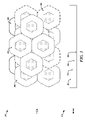
図1は、充電面を提供するように展開および/または構成された充電セル100の一例を示している。この例では、充電セル100が、電力伝送領域104において電磁場を生成するのに十分な電流を受け取ることができる導体、ワイヤまたは回路基板トレースを使用して構成された1または複数のコイル102を取り囲む実質的に六角形の形状を有する。様々な実施形態では、いくつかのコイル102が、図1に示す六角形の充電セル100を含む、実質的に多角形の形状を有することができる。他の実施形態では、他の形状を有するコイル102を提供するようにしてもよい。コイル102の形状は、少なくとも部分的に、製造技術の能力または制限によって、かつ/またはプリント回路基板などの基板106上の充電セルのレイアウトを最適化するために、決定することができる。各コイル102は、ワイヤ、プリント回路基板トレースおよび/または他のコネクタを使用して、螺旋状に実装されるようにしてもよい。各充電セル100は、様々な層のコイル102が共通の軸108を中心にして配置されるように、絶縁体または基板106によって分離された2つ以上の層に跨がるようにしてもよい。
FIG. 1 illustrates an
図2は、本明細書に開示される特定の態様に従って構成された充電面のセグメントの単一層上に提供される充電セル202の配置200の一例を示している。充電セル202は、ハニカムパッケージ形態に従って配置されている。この例では、充電セル202が、重なり合うことなく端と端を並べて配置されている。この配置は、スルーホールまたはワイヤ相互接続なしで提供することができる。充電セル202の一部が重なる配置を含む他の配置も可能である。例えば、2以上のコイルのワイヤがある程度交互に配置されるようにしてもよい。
FIG. 2 illustrates an
図3は、本明細書に開示される特定の態様に従って構成された充電面のセグメント内に複数の層が重なり合う場合の、2つの視点300、310からの充電セルの配置の一例を示している。充電セルの層302、304、306、308が、充電面のセグメント内に提供されている。充電セルの各層302、304、306、308内の充電セルは、ハニカムパッケージ形態に従って配置されている。一例では、充電セルの各層302、304、306、308が、4以上の層を有するプリント回路基板上に形成されるものであってもよい。充電セル100の配置は、図示されたセグメントに隣接する指定された充電領域を完全にカバーするように選択することができる。
FIG. 3 shows an example of charging cell placement from two
図4は、本明細書に開示される特定の態様に従って構成された複数の層の充電セルを採用する充電面400において提供される電力伝送領域の配置を示している。図示された充電面は、充電セルの4つの層402、404、406、408から構成されている。図4において、充電セルの第1の層402の充電セルによって提供される各電力伝送領域が「L1」とマークされ、充電セルの第2の層404の充電セルによって提供される各電力伝送領域が「L2」とマークされ、充電セルの第3の層406、408の充電セルによって提供される各電力伝送領域が「L3」とマークされ、充電セルの第1の層408の充電セルによって提供される各電力伝送領域が「L4」とマークされている。
FIG. 4 illustrates an arrangement of power transfer areas provided in a charging
充電面でのデバイスの位置特定
本明細書に開示される特定の態様によれば、位置検知は、充電セル内にコイルを形成する導電体のいくつかの特性の変化に依存するものであってもよい。導電体の特性の測定可能な違いは、静電容量、抵抗、インダクタンスおよび/または温度を含むことができる。いくつかの実施例では、充電面の負荷が、負荷ポイントの近傍に位置するコイルの測定可能な抵抗に影響を与える。いくつかの実施形態では、接触、圧力、負荷および/または歪みの変化を検出することによって位置検知を可能にするために、センサを提供することができる。
Device Location on Charging Surface According to certain aspects disclosed herein, location sensing relies on changes in some properties of the electrical conductors that form the coils within the charging cell. good too. The measurable differences in properties of the conductors can include capacitance, resistance, inductance and/or temperature. In some embodiments, the load on the charging surface affects the measurable resistance of coils located near the load point. In some embodiments, sensors can be provided to enable position sensing by detecting changes in contact, pressure, load and/or strain.
本明細書に開示される特定の態様は、差動容量検知技術を使用して、充電面上に自由に配置され得る低電力デバイスの位置を検知することができる装置および方法を提供する。図5は、モバイル通信デバイスまたは他の物体512の位置および/または向きを検出するための差動容量検知の使用の例500を示している。1または複数のコイル504は、プリント回路基板502、基板または他のタイプのキャリアの表面上に提供されている。容量性結合(破線510で図示)は、コイル504のペア間で測定可能な実効静電容量508に起因することができる。静電容量は、コイル504の各々に結合された回路を用いて測定することができる。充電可能なデバイスなどの物体512は、コイル504のペア間の見かけ上の静電容量508を増加または減少させることができる。物体512は、コイル504のペア間の容量性結合(破線520で図示)を変更し得る。一例では、物体512が、オーバーレイ506の誘電特性に影響を与え、物体512を介して代替的な容量性回路を提供し、かつ/またはコイル504のペア間の静電容量508の測定値または見かけの値を増加または減少させる電気的特性の他の変化をもたらし得る。物体512によって引き起こされる測定された差を、差動容量と呼ぶことがある。
Certain aspects disclosed herein provide apparatus and methods that can sense the position of low power devices that can be freely placed on a charging surface using differential capacitive sensing techniques. FIG. 5 shows an example 500 of using differential capacitive sensing to detect the position and/or orientation of a mobile communication device or
充電デバイスは、本明細書に開示される特定の態様に従って提供されるコイルアレイを含む充電面上の任意の場所でデバイスを見付けるために、差動容量検知を使用することができる。その後、充電デバイスは、受信デバイスとも称されるデバイスの最適な充電を提供するために使用することができるコイル504のうちの1または複数を決定することができる。
A charging device can use differential capacitive sensing to locate the device anywhere on the charging surface, including coil arrays provided according to certain aspects disclosed herein. The charging device can then determine one or more of the
差動容量検知の使用により、従来の検出技術と比較して、極めて低い電力での検出および位置特定動作が可能になる。デバイスを検出するために現在のワイヤレス充電アプリケーションで使用されている従来技術は、送信コイルを駆動してかなりの電力(例えば、100~200mW)を消費する「ping」方式を採用している。送信コイルによって生成された場は、受信デバイスを検出するために使用される。差動容量検知は、受信デバイスの存在を検出するために送信コイルに電力を供給する必要がなく、追加の検知要素を必要としない。コイルアレイで使用されるコイルは、受信デバイスを見付けるために、かつ/または受信デバイスの物理的位置を特定するために使用される容量性検知要素として機能することができる。 The use of differential capacitive sensing allows for extremely low power sensing and locating operations compared to conventional sensing techniques. Conventional technology used in current wireless charging applications to detect devices employs a “ping” scheme that drives a transmit coil and consumes significant power (eg, 100-200 mW). The fields produced by the transmit coils are used to detect receiving devices. Differential capacitive sensing does not require powering the transmit coil and does not require additional sensing elements to detect the presence of a receiving device. Coils used in coil arrays can function as capacitive sensing elements used to locate and/or identify the physical location of a receiving device.
差動容量検知は、2つの隣接するコイル間の差動容量を測定することで動作する。静電容量の差および/または変化により、グランドプレーンや追加の導電性検知要素を必要とせずに、受信デバイスの存在を識別することができる。差動容量検知は、pingに応答して受信デバイスによって送信される応答を待つ必要性を排除することによって、受信デバイスの迅速な検出を可能にする高速な方法を提供する。また、差動容量検知は、充電デバイスからのpingまたはクエリに応答するための蓄積電力が不足している受信デバイスを検知することができる。 Differential capacitive sensing operates by measuring the differential capacitance between two adjacent coils. Differences and/or changes in capacitance can identify the presence of a receiving device without the need for ground planes or additional conductive sensing elements. Differential capacitive sensing provides a fast method of enabling rapid detection of a receiving device by eliminating the need to wait for a response sent by the receiving device in response to a ping. Differential capacitive sensing can also detect receiving devices that lack stored power to respond to pings or queries from charging devices.
特定の態様によれば、受信デバイスの存在、位置および/または向きは、例えば静電容量、抵抗、インダクタンス、接触、圧力、温度、負荷、歪みの差または変化を検出することを伴う、差動容量検知または別の位置検知手法、および/または別の適切な種類の検知を使用して判定することができる。位置検知を利用して、充電されるデバイスの大凡の位置を判定し、互換性のあるデバイスが充電面上に配置されたか否かを充電デバイスが判定することができる。例えば、充電デバイスは、互換性のあるデバイスが充電面上に置かれたことを、互換性のあるデバイスに応答させる断続的なテスト信号(ping)を送信することによって判定することができる。充電デバイスは、規格、慣例、製造業者またはアプリケーションによって規定された応答信号の受信を判定した後に、少なくとも1の充電セル内の1または複数のコイルを作動させるように構成されるものであってもよい。いくつかの例では、互換性のあるデバイスは、充電デバイスが互換性のあるデバイスを充電するために使用される最適な充電セルを見付けることができるように、受信した信号強度を伝達することによって、pingに応答することができる。 According to certain aspects, the presence, position and/or orientation of the receiving device can be detected differentially, e.g., involving detecting differences or changes in capacitance, resistance, inductance, contact, pressure, temperature, load, strain. It can be determined using capacitive sensing or another position sensing technique and/or another suitable type of sensing. Position sensing can be used to determine the approximate location of the device being charged so that the charging device can determine if a compatible device has been placed on the charging surface. For example, a charging device may determine that a compatible device has been placed on the charging surface by sending an intermittent test signal (ping) that causes the compatible device to respond. The charging device may be configured to activate one or more coils in at least one charging cell after determining receipt of a response signal defined by a standard, practice, manufacturer or application. good. In some instances, the compatible device communicates received signal strength so that the charging device can find the best charging cell to use to charge the compatible device. , can respond to pings.
一例では、コントローラ、状態機械または他の処理装置は、充電セル内の1または複数のコイルに起因する静電容量を測定し、測定した静電容量が受信デバイスまたは受信デバイス内の対応するコイルの近接を示しているか否かを判定するように構成することができる。いくつかの実施形態では、静電容量を、検知回路における静電容量の差として測定することができる。コントローラ、状態機械または他の処理装置は、受信デバイスが存在しない場合に、各充電セルに付随する予測静電容量を識別する情報を保持することができる。その後、測定した静電容量の差は、受信デバイスが充電セルの近傍に位置していることを判定するために使用することができる。差の大きさは、充電セルと受信デバイスとの間の距離を示す可能性がある。 In one example, the controller, state machine, or other processing device measures the capacitance attributed to one or more coils in the charging cell, and the measured capacitance is the receiving device or corresponding coils in the receiving device. It can be configured to determine whether it indicates proximity. In some embodiments, capacitance can be measured as a difference in capacitance in a sensing circuit. A controller, state machine, or other processing device may maintain information identifying the expected capacitance associated with each charge cell in the absence of a receiving device. The measured capacitance difference can then be used to determine when the receiving device is located in proximity to the charging cell. The magnitude of the difference can indicate the distance between the charging cell and the receiving device.
いくつかの実施形態では、コントローラ、状態機械または他の処理装置が、充電面の1または複数のプロファイルを維持することができる。プロファイルは、個別の充電セルまたはグループを、予測される静電容量の測定値、最後に測定された静電容量および/または受信デバイスが存在するときの静電容量値の過去の尤度に関連付けることができる。 In some embodiments, a controller, state machine, or other processing device can maintain one or more profiles of the charging surface. The profile associates individual charge cells or groups with expected capacitance measurements, last measured capacitance and/or historical likelihood of capacitance values in the presence of a receiving device. be able to.
特定の態様によれば、受信デバイスの存在、位置および/または向きは、探索パターンを使用して静電容量の差について充電セルを探索することによって判定することができる。探索パターンは、充電デバイスを検出する平均時間を改善するために、擬似ランダムにすることができる。いくつかの実施形態では、探索の開始点が、受信デバイスが近接位置にあって充電を受けているときに捕捉された測定の履歴に基づいて選択されるものであってもよい。いくつかの実施形態では、受信デバイスが近接位置にあって充電を受けているときに捕捉された測定の履歴に基づいて探索するために、充電セルの初期グループが優先されるようにしてもよい。 According to certain aspects, the presence, location and/or orientation of a receiving device can be determined by searching the charge cells for capacitance differences using a search pattern. The search pattern can be pseudo-random to improve the average time to detect charging devices. In some embodiments, the starting point for the search may be selected based on a history of measurements taken while the receiving device was in proximity and receiving charge. In some embodiments, an initial group of charged cells may be prioritized for searching based on a history of measurements taken while the receiving device was in close proximity and receiving charging. .
図6は、複数のコイル602、604、606、608、622、624、626、628を含むコイルのグループで実行される探索の特定の態様を示している。いくつかの実施形態では、コイルの異なるグループ600、620の測定可能な特性の差を測定することによって、探索が実行されるものであってもよい。図示された例では、コイル602、604、606、608を含むコイルの第1のグループ600の複合特性が、コイル622、624、626、628を含むコイルの第2のグループ620の複合特性とは独立して評価されるものであってもよい。コイルのグループ600、620は、集約によって測定される量を増加させるように、または単一の測定中により広い領域をカバーするように選択されるものであってもよい。一例では、コイルのスタックに関連する静電容量が、総計として測定されるものであってもよい。別の例では、充電面の様々な位置にあるコイルの静電容量を測定して、測定したコイルによって処理される充電面上に置かれた充電されるデバイスの迅速な検出を可能にすることができる。
FIG. 6 illustrates a particular aspect of a search performed on a group of coils including a plurality of coils 602,604,606,608,622,624,626,628. In some embodiments, the search may be performed by measuring differences in measurable properties of
図7および図8は、差動容量検知を使用して実行される探索の特定の態様を示している。図7は、図示した3つの充電コイル706、708、710を含む1または複数の充電セルが設けられた充電面700の2次元図(X軸702およびY軸704)を示している。図7に示す特定の態様は、充電コイル706、708、710内の個々のコイルを含む探索、または充電面700全体に広がる探索、および/または三次元空間内の探索にも適用可能である。図示の例では、充電コイル706、708、710は、擬似ランダム探索として実行することができる、探索中にテストされる最初の3つの充電コイルである。探索は、第1の充電コイル706から始まる。探索パターンは、テストを第2の充電コイル708に移動(712m)させ、その後、テストを第3の充電コイル710に移動(714)させることができる。探索は、受信デバイスの概略位置を特定するために実行するようにしてもよく、また、受信デバイスの存在を示す測定値が得られたときに停止するようにしてもよい。その後、第2の領域固有の探索を、充電コイル706、708、710の周囲で実行するようにしてもよい。
Figures 7 and 8 illustrate a particular aspect of searching performed using differential capacitive sensing. FIG. 7 shows a two-dimensional view (
図8は、充電されるデバイスが充電面上に配置されたか否か、またはどこに配置されたのかを判定するために、充電デバイスによって実行され得る探索プロセスを例示するフローチャート800である。フローチャート800は、充電デバイス内に提供される個々のコイル、共通の軸に沿って近接してスタックされたたコイルのグループ、および/または単一の充電コイル706、708、710に提供されるコイルのグループ、または充電面の関心領域の処理を担うコイルのグループに関連するものであってもよい(FIG6も参照されたい)。
FIG. 8 is a
ブロック802では、初期コイルまたはコイルのグループが、探索の開始点として選択される。開始点は、疑似乱数発生器などを使用して選択することができる。いくつかの例では、充電されるデバイスが存在する可能性が高い位置の近くにあることが分かっているか又は予測される潜在的な開始点のグループのなかから開始点が選択されるものであってもよい。例えば、充電デバイスは、充電されたデバイスの位置および/またはデバイスを充電するために最も頻繁に起動される充電コイルまたは充電セルを特定する探索および/または充電イベントの履歴を維持することができる。
At
ブロック804では、充電デバイスが、1または複数のコイル内の導体の静電容量の測定値、または、充電されるデバイスの存在下で変化する可能性のあるコイルまたは充電面に関連する他のいくつかの特性の測定値を取得することができる。充電デバイスは、測定した特性値が、以前測定した特性値、公称値および/または充電面の異なる部位で測定した値から変化したか否かを判定することができる。 At block 804, the charging device receives a measurement of the capacitance of the conductors in one or more coils, or some other value associated with the coil or charging surface that may change in the presence of the device being charged. It is possible to obtain measurements of any property. The charging device can determine whether the measured property value has changed from a previously measured property value, a nominal value, and/or a value measured at a different portion of the charging surface.
ブロック804で変化が検出された場合、充電デバイスは、ブロック808で充電面のプロファイルを更新することができる。例えば、プロファイルは、新しい値および/または値の変化の大きさを反映するように変更することができる。プロファイルは、充電されるデバイスの潜在的な位置をマッピングするために、かつ/または充電面から移動または除去されたデバイスを再マッピングまたはアンマップするために使用することができる。いくつかの実施形態では、測定した特性値の変化または差の検出により、変化またはトリガ特性値を示した充電コイルを使用して、充電デバイスにpingを開始させるようにしてもよい。ブロック806で変化が検出されなかった場合、またはブロック808で充電プロセスが開始されなかった場合、ブロック810で探索を継続するようにしてもよい。
If a change is detected at block 804 , the charging device may update the profile of the charging surface at
ブロック810では、充電デバイスが、次に測定されるコイルを選択することができる。次のコイルを選択するために疑似乱数発生器を使用して、疑似乱数シーケンスに基づいて選択を行うことができる。ブロック812では、テストされるべきすべてのコイルがテストされたと判定された場合、探索を終了することができる。テストされる追加のコイルが残っている場合、ブロック804では探索を継続することができる。
At
探索が充電面上の潜在的なデバイスの配置を特定すると、充電デバイスは、ping手順を開始して、充電面上に配置されたデバイスを充電するために作動される充電セル、充電セルの組合せおよび/またはコイルの組合せを特定することができる。ping手順は、充電されるデバイスが充電デバイスと互換性があることを検証し、pingを送信するために使用されるコイルが、要求された又は所望の充電手順に対して最適な位置にあるか否かを示す信号強度を特定することができる。 Once the probing identifies potential device locations on the charging surface, the charging device initiates a ping procedure to determine which charging cell, combination of charging cells, is activated to charge the device located on the charging surface. and/or combinations of coils can be specified. The ping procedure verifies that the device being charged is compatible with the charging device and whether the coil used to send the ping is optimally positioned for the requested or desired charging procedure. A signal strength can be specified that indicates whether or not
pingを使用してデバイスがワイヤレス充電デバイスから充電を受信するように構成されていることを確認する前に、複数コイルのフリーポジション充電パッドの上または近くに配置されたデバイスを見付けるために探索を実行すると、大幅な電力の節約を実現することができる。探索でデバイスが検出されるまでpingを提供することを控えるとともに、検出されたデバイスに近接して配置されて、検出されたデバイスと電磁充電接続を確立できる可能性が高い送信コイルにping送信を制限することによって、消費電力の節約を実現することができる。 Use a probe to find a device placed on or near a multi-coil free-position charging pad before using ping to verify that the device is configured to receive charge from a wireless charging device. By doing so, significant power savings can be realized. Refrain from providing pings until the device is detected in a probe, and ping transmit coils that are placed in close proximity to the detected device and are likely to establish an electromagnetic charging connection with the detected device. By limiting, power consumption savings can be realized.
パッシブPing
ワイヤレス充電デバイスは、従来のping送信に取って代わることができかつ/または補足することができる低電力発見手法をサポートするように、本明細書に開示される特定の態様に従って適合させることができる。従来のpingは、基地局の送信コイルを含む共振LC回路を駆動することによって生成される。その後、基地局は、受信デバイスからのASK変調応答を待つ。低電力発見手法は、パッシブpingを利用して、高速および/または低電力発見を提供することができる。特定の態様によれば、共振LC回路を含むネットワークを、少量のエネルギーを含む高速パルスで駆動することによって、パッシブpingを生成することができる。高速パルスは、共振LC回路を励起し、注入されたエネルギーが減衰して消散するまで、ネットワークをその固有の共振周波数で発振させる。一例では、高速パルスが、ネットワークおよび/または共振LC回路の共振周波数の半周期に対応する持続時間を有することができる。基地局が100kHz~200kHzの周波数範囲内の電力をワイヤレス伝送するように構成されている場合、高速パルスは、2.5μs未満の持続時間を有することができる。
Passive Ping
A wireless charging device can be adapted according to certain aspects disclosed herein to support low power discovery techniques that can replace and/or supplement traditional ping transmissions. . A conventional ping is generated by driving a resonant LC circuit that includes the base station's transmit coil. The base station then waits for an ASK modulated response from the receiving device. Low power discovery techniques can utilize passive pings to provide fast and/or low power discovery. According to certain aspects, a passive ping can be generated by driving a network containing a resonant LC circuit with a fast pulse containing a small amount of energy. The fast pulse excites a resonant LC circuit, causing the network to oscillate at its natural resonant frequency until the injected energy decays and dissipates. In one example, the fast pulse can have a duration corresponding to half the period of the resonant frequency of the network and/or resonant LC circuit. If the base station is configured to wirelessly transmit power in the 100 kHz to 200 kHz frequency range, the fast pulse may have a duration of less than 2.5 μs.
パッシブpingは、共振LC回路を含むネットワークがリンギングする固有周波数と、ネットワーク内のエネルギーの減衰率とに基づいて、特徴付けることができ、かつ/または構成することができる。ネットワークおよび/または共振LC回路のリンギング周波数は、次のように定義することができる。

減衰率は、次式で定義されるように、発振器ネットワークのQ値によって制御される。

式1および式2は、共振周波数がLおよびCによって影響を受け、Q値がL、C、Rによって影響を受けることを示している。本明細書に開示される特定の態様に従って提供される基地局において、ワイヤレスドライバは、共振コンデンサの選択によって決定される固定値のCを有する。LおよびRの値は、ワイヤレス送信コイルと、ワイヤレス送信コイルに隣接して配置された物体またはデバイスとによって決定される。
ワイヤレス送信コイルは、送信コイルに近接して配置されたデバイスの受信コイルと磁気的に結合し、そのエネルギーの一部を充電される近接デバイスに結合するように構成されている。送信回路のL値およびR値は、充電されるデバイスの特性、および/または送信コイルの近接範囲内の他の物体によって影響を受ける可能性がある。例えば、高い透磁率を有する一片の鉄材料が送信コイルの近くに配置された場合、送信コイルの総インダクタンス(L)が増加し、その結果、式1で示すように、共振周波数が低くなる可能性がある。渦電流誘導による材料の加熱によって一部のエネルギーが失われる可能性があり、それらの損失が、式2で示すように、Rの値を増加させ、それによりQ値を低下させることで特徴付けられる。 The wireless transmit coil is configured to magnetically couple with the receive coil of a device placed in proximity to the transmit coil and couple a portion of its energy into the proximate device to be charged. The L and R values of the transmit circuit can be affected by the characteristics of the device being charged and/or other objects within close range of the transmit coil. For example, if a piece of ferrous material with high magnetic permeability is placed near the transmit coil, the total inductance (L) of the transmit coil can increase, resulting in a lower resonant frequency, as shown in Eq. have a nature. Some energy may be lost by heating the material due to eddy current induction, and these losses are characterized by increasing the value of R and thereby decreasing the Q value, as shown in Eq. be done.
また、送信コイルに近接して配置されたワイヤレス受信機も、Q値および共振周波数に影響を与える可能性がある。受信機は、高いQを有する調整されたLCネットワークを含み、それによりQ値がより低い送信コイルをもたらす可能性がある。送信コイルの共振周波数は、受信機に磁性材料が追加されることにより低下する場合があり、その磁性材料が全磁気システムの一部となる。表1は、送信コイルのすぐ近くに配置された様々なタイプの物体に起因する特定の影響を示している。

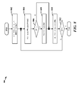
図9は、充電器基地局に設けることができるワイヤレス送信機900を示している。コントローラ902は、フィルタ回路908によってフィルタリングまたは他の方法で処理されたフィードバック信号を受信することができる。コントローラは、コンデンサ912およびインダクタ914を含む共振回路906に交流電流を供給するドライバ回路904の動作を制御することができる。電圧916は、共振回路906のLCノード910で測定される。
FIG. 9 shows a
パッシブping技術は、LCノード910で測定または観察された電圧および/または電流を使用して、本明細書に開示される特定の態様に従って構成されたデバイスの充電パッドに近接する受信コイルの存在を識別することができる。多くの従来のワイヤレス充電器送信機では、LCノード910での電圧またはネットワーク内の電流を測定するための回路が提供される。それら電圧および電流は、電力調整の目的で、かつ/またはデバイス間の通信をサポートするために、監視することができる。図9に示す例では、LCノード910における電圧が示されているが、追加的または代替的には、パッシブpingをサポートするために電流が監視されることが考えられる。パッシブpingに対する共振回路906の応答(初期電圧V0)は、以下のように、LCノード910における電圧(VLC)によって表すことができる。
![]()
![]()
図10は、パッシブpingに対する応答1000が式3に従って減衰する第1の例を示している。時間=0における励起パルスの後、電圧および/または電流は、式1によって定義された共振周波数で、式3によって定義された減衰率で発振することが分かる。発振の最初のサイクルは、電圧レベルV0から始まり、VLCは、Q値およびωにより制御されてゼロまで減衰し続ける。図10に示す例は、充電パッドに物体が存在しないか又は近くにないときの典型的なオープンまたは無負荷の応答を表している。図10では、Q値が20であると仮定している。
FIG. 10 shows a first example where the
図11は、パッシブpingに対する応答1100が式3に従って減衰する第2の例を示している。時間=0における励起パルスの後、電圧および/または電流は、式1によって定義される共振周波数で、式3によって定義される減衰率で発振することが分かる。発振の最初のサイクルは、電圧レベルV0から始まり、VLCは、Q値およびωによって制御されてゼロまで減衰し続ける。図11に示す例は、充電パッドに物体が存在するか又は近接してコイルに負荷がかかるときの負荷応答を示している。図10では、Q値が7になることがある。VLCは、電圧応答1000に対して、電圧応答1100でより高い周波数で発振する。
FIG. 11 shows a second example where the
図12は、応答1200、1220、1240の違いが観察される一組の例を示している。2.5μsよりも短いパルスを使用してドライバ回路904が共振回路906を励起すると、パッシブpingが開始される。異なるタイプのワイヤレス受信機および送信機上に置かれた異物は、LCノード910における電圧または送信機の共振回路906における電流において観察可能な異なる応答をもたらす。この差異は、V0の発振の共振回路906周波数のQ値の変化を示し得る。表2は、開状態に関連して充電パッドに置かれた物体の特定の例を示している。

表2において、Q値は以下のように計算される。
![]()
ここで、Nは、励振から振幅が0.5V0未満になるまでのサイクル数である。
In Table 2, the Q value is calculated as follows.
![]()
where N is the number of cycles from excitation until the amplitude is less than 0.5V0 .
図13は、本明細書に開示される特定の態様に従って構成されたワイヤレス充電デバイスに実装されるパッシブpingを含む方法を示すフローチャート1300である。ブロック1302では、コントローラが、短い励起パルスを生成し、その短い励起パルスを共振回路を含むネットワークに提供することができる。ネットワークは、公称共振周波数を有し、短い励起パルスは、ネットワークの公称共振周波数の半分未満の持続時間を有することができる。公称共振周波数は、共振回路の送信コイルが、充電されるデバイス内の鉄製の物体、非鉄製の物体および/または受信コイルを含む外部物体から隔離されているときに観察される。
FIG. 13 is a
ブロック1304では、コントローラは、ネットワークの共振周波数を求めることができ、あるいはパルスに応答するネットワークの共振の減衰を監視することができる。本明細書に開示される特定の態様によれば、デバイスまたは他の物体が送信コイルに近接して配置されたときに、ネットワークに関連付けられた共振周波数および/またはQ値が変化し得る。共振周波数は、共振回路の送信コイルが外部物体から隔離されているときに観察される公称共振周波数から増加または減少し得る。ネットワークのQ値は、共振回路の送信コイルが外部物体から隔離されているときに測定可能な公称Q値に対して増加または減少し得る。本明細書に開示される特定の態様によれば、Q値の違いが、公称Q値に関連付けられた遅延に対して共振回路における発振の振幅の減衰を延長または加速するとき、遅延の持続時間は、送信コイルに近接して配置された物体の存在またはタイプを示し得る。
At
一例では、コントローラが、コンパレータなどを用いてLCノード910における電圧を示す信号のゼロ交差を検出するように構成された遷移検出回路を使用して、ネットワークの共振周波数を求めることができる。いくつかの実施形態では、直流(DC)成分を信号からフィルタリングしてゼロ交差を提供することができる。いくつかの実施形態では、コンパレータが、オフセットを使用してDC成分を考慮し、共通の電圧レベルの交差を検出することができる。検出したゼロ交差をカウントするために、カウンタを用いることができる。別の例では、コントローラが、LCノード910における電圧を示す信号によって閾値電圧を通る交差を検出するように構成された遷移検出回路を使用してネットワークの共振周波数を求めることができ、ここで、信号の振幅が、論理回路によって検出および監視することができる電圧の範囲内でクランプまたは制限される。この例では、信号の遷移をカウントするためにカウンタを用いることができる。ネットワークの共振周波数は、他の方法を用いて測定、推定および/または計算されるものであってもよい。
In one example, the controller can determine the resonant frequency of the network using a transition detection circuit configured to detect zero crossings of a signal indicative of the voltage at
別の例では、タイマまたはカウンタを使用して、電圧レベルV0から閾値電圧レベルまでVLCが減衰するまでの経過時間を測定することができる。経過時間は、ネットワークの減衰特性を表すために使用することができる。閾値電圧レベルは、カウンタまたはタイマがパルスに対する様々な応答1200、1220、1240を区別することを可能にするのに十分な粒度を提供するように選択することができる。VLCは、検出または測定されたピーク、ピークトゥピーク、包絡線および/または整流された電圧レベルによって表すことができる。ネットワークの減衰特性は、他の方法を用いて測定、推定および/または計算されるものであってもよい。
In another example, a timer or counter can be used to measure the elapsed time for VLC to decay from the voltage level V0 to the threshold voltage level. Elapsed time can be used to represent the decay properties of the network. The threshold voltage level can be selected to provide sufficient granularity to allow the counter or timer to distinguish between
ブロック1306において、コントローラは、公称共振周波数に対する共振周波数の変化が、送信コイルに近接した物体の存在を示していると判定した場合に、ブロック1312において、物体の識別を試みることができる。ブロック1306において、コントローラは、共振周波数が公称共振周波数と実質的に同じであると判定した場合、ブロック1308において、共振回路における発振の振幅の減衰特性を考慮することができる。コントローラは、周波数が公称共振周波数を中心とする規定された周波数範囲内または公称共振周波数を含む規定された周波数範囲内に留まる場合に、ネットワークの共振周波数が公称共振周波数と実質的に同じであると判定することができる。いくつかの実施形態では、コントローラが、共振周波数および減衰特性の変化を用いて物体を識別することができる。それらの後の実施形態では、コントローラが、共振周波数に関係なくブロック1308を続けることができ、送信コイルに近接して配置された物体を識別するときに、共振周波数の変化を追加のパラメータとして使用することができる。
If at
ブロック1308において、コントローラは、タイマを使用することができ、かつ/または、初期VO振幅と、減衰特性を評価するために使用される閾値振幅との間に経過した共振回路内の発振の周期をカウントすることができる。一例では、VO/2を閾値振幅として選択することができる。ブロック1310では、初期VO振幅と閾値振幅との間のサイクル数または経過時間を使用して、共振回路における発振振幅の減衰を特徴付けることができ、特徴付けた減衰を対応する公称減衰特性と比較することができる。ブロック1310において、周波数および遅延特性の変化が検出されない場合、コントローラは、送信コイルの近くに物体が配置されていないと判定して、手順を終了することができる。ブロック1310において、周波数および/または遅延特性の変化が検出された場合、コントローラは、ブロック1312において、物体を識別することができる。
At
ブロック1312において、コントローラは、充電パッド上に配置された受信デバイスを識別するように構成されるものであってもよい。コントローラは、他のタイプの物体、または、例えばパッシブpingを提供する送信コイルと位置がずれている受信デバイスを含む、充電パッド上に最適に配置されていない受信デバイスを無視するように構成されるものであってもよい。いくつかの実施形態では、コントローラは、共振周波数、減衰時間、共振周波数の変化、減衰時間の変化および/またはQ値の推定値によってインデックス化されたルックアップテーブルを使用することができる。ルックアップテーブルは、特定のデバイスのタイプを識別する情報、および/または識別したデバイスまたはデバイスのタイプを充電する際に使用される充電パラメータを提供することができる。
At
パッシブpingは、共振回路906のLCノード910で観測される公称共振周波数の半周期未満であり得る非常に短い励起パルスを使用する。従来のpingは、16,000周期以上にわたって、送信コイルを能動的に駆動することがある。従来のpingによって消費される電力および時間は、数桁のオーダーでパッシブpingの電力および時間の使用を超える可能性がある。例えば、パッシブpingは、最大ping時間が約100μsで、pingあたり約0.25μJを消費し、一方、従来のアクティブpingは、最大ping時間が約90msで、pingあたり約80mJを消費する。この例では、エネルギー散逸を320,000分の1に削減することができ、pingあたりの時間を900分の1に削減することができる。
Passive pings use very short excitation pulses that can be less than half the period of the nominal resonant frequency observed at
また、パッシブpingは、静電容量検知などの別の低電力検知方法と組み合わせることもできる。静電容量検知などは、充電面に近接している物体の存在の有無を判定する超低電力検出方法を提供することができる。静電容量式検出の後、パッシブpingを各コイル上で順次または同時に送信して、潜在的な受信デバイスおよび/または物体がどこに位置しているかのより正確なマップを生成することができる。パッシブping手順が実行された後、最も可能性の高いデバイスの位置でアクティブpingを提供するようにしてもよい。デバイスの位置検知、識別および充電のための例示的なアルゴリズムが、図14に示されている。 Passive pings can also be combined with other low power sensing methods such as capacitive sensing. Capacitive sensing or the like can provide an ultra-low power detection method for determining the presence or absence of an object in proximity to the charging surface. After capacitive detection, passive pings can be sent on each coil sequentially or simultaneously to generate a more accurate map of where potential receiving devices and/or objects are located. After the passive ping procedure has been performed, an active ping may be provided at the most likely location of the device. An exemplary algorithm for device location, identification and charging is shown in FIG.
図14は、本明細書に開示される特定の態様に従って実装されるワイヤレス充電デバイスによって採用され得る複数の検知および/または問合せ技術を含む電力伝送管理手順を示すフローチャート1400である。この手順は、定期的に開始することができ、いくつかの実施例では、ワイヤレス充電デバイスが低電力またはスリープ状態を終了した後に開始することができる。一例では、充電パッド上へのデバイスの配置に対して1秒未満の応答を提供するように計算された周波数で、この手順を繰り返すことができる。この手順は、当該手順の最初の実行中にエラー状態が検出された場合、かつ/または充電パッド上に配置されたデバイスの充電が完了した後に、再実行することができる。
FIG. 14 is a
ブロック1402において、コントローラは、静電容量式近接検知を使用して初期探索を実行することができる。静電容量式近接検知は、迅速かつ低電力で実行することができる。一例では、静電容量式近接検知が反復的に実行され、ここでは、1または複数の送信コイルが各反復でテストされる。各反復でテストされる送信コイルの数は、コントローラが利用できる検知回路の数によって決定されるものであってもよい。ブロック1404において、コントローラは、静電容量式近接検知が、送信コイルの1つに近接する物体の存在または潜在的な存在を検出したか否かを判定することができる。静電容量式近接検知によって物体が検出されなかった場合、コントローラは、ブロック1424において、充電デバイスを低電力状態、アイドル状態および/またはスリープ状態にするようにしてもよい。物体が検出された場合、コントローラは、ブロック1406において、パッシブping検知を開始することができる。
At
ブロック1406において、コントローラは、1または複数の送信コイルの近くに物体が存在することを確認するために、かつ/または近接して配置された物体の性質を評価するために、パッシブping検知を開始することができる。パッシブping検知は、同様の量の電力を消費するが、静電容量式近接検知よりも長い時間がかかる可能性がある。一例では、各パッシブpingが約100μsで完了し、0.25μJを消費する。パッシブpingは、静電容量式近接検知によって対象であると識別された各送信コイルに提供するようにしてもよい。いくつかの実施形態では、重ね合わされた送信コイルを含む、静電容量式近接検知によって対象であると識別された各送信コイルの近くの送信コイルにパッシブpingを提供するようにしてもよい。ブロック1408において、コントローラは、パッシブping検知が、受信デバイスである可能性のある送信コイルの1つに近接する潜在的に充電可能なデバイスの存在を検出したか否かを判定することができる。潜在的に充電可能なデバイスが検出された場合、コントローラは、ブロック1410において、アクティブデジタルping検知を開始するようにしてもよい。潜在的に充電可能なデバイスが検出されていない場合、ブロック1406において、すべてのコイルがテストされるまで、かつ/またはコントローラがパッシブping検知を終了するまで、パッシブping検知を継続することができる。一例では、コントローラは、すべての送信コイルがテストされた後に、パッシブping検知を終了する。パッシブping検知が潜在的に充電可能なデバイスを見付けることができない場合、コントローラは、充電デバイスを低電力状態、アイドル状態および/またはスリープ状態に移行させることができる。いくつかの実施形態では、潜在的に充電可能なデバイスが検出されたときに、アクティブpingを使用して潜在的に充電可能なデバイスを問い合わせることができるように、パッシブping検知が一時停止されるようにしてもよい。パッシブping検知は、アクティブpingの結果が得られた後に再開することができる。
At
ブロック1410において、コントローラは、アクティブpingを使用して、潜在的に充電可能なデバイスを問い合わせることができる。アクティブpingは、パッシブping検知によって識別された送信コイルに提供されるようにしてもよい。一例では、規格で規定されたアクティブping交換が、約90msで完了し、80mJを消費する。アクティブpingは、潜在的に充電可能なデバイスに関連付けられた各送信コイルに提供されるようにしてもよい。
At
ブロック1412において、コントローラは、充電可能なデバイスを識別し、設定することができる。ブロック1410で提供されるアクティブpingは、充電可能なデバイスを識別する情報を含む応答を送信するように充電可能なデバイスを促すように構成されるものであってもよい。いくつかの実施形態では、コントローラは、パッシブpingによって検出された潜在的に充電可能なデバイスを識別または設定することができない場合もあり、コントローラは、ブロック1406において、パッシブpingに基づく探索を再開することができる。ブロック1414において、コントローラは、ベースライン充電プロファイルまたはネゴシエートした充電プロファイルを、識別した充電可能なデバイスを充電するために使用すべきかどうかを判定することができる。ベースラインまたはデフォルト充電プロファイルは、規格によって規定されるものであってもよい。一例では、ベースライン充電プロファイルが、充電電力を5Wに制限する。別の例では、ネゴシエートした充電プロファイルが、最大15Wで充電を行うことを可能にする。ベースライン充電プロファイルが選択されると、コントローラは、ブロック1420で電力の伝送(充電)を開始することができる。
At
ブロック1416において、コントローラは、電力伝送を最適化することができる規格で規定されたネゴシエーションおよびキャリブレーションプロセスを開始してもよい。コントローラは、充電可能なデバイスとネゴシエートして、ベースライン充電プロファイルに対して規定された電力プロファイルとは異なる拡張電力プロファイルを決定することができる。コントローラは、ブロック1418において、ネゴシエーションおよびキャリブレーションプロセスが失敗したと判定し、電力伝送管理手順を終了することができる。ブロック1418でコントローラがネゴシエーションおよびキャリブレーションプロセスが成功したと判定した場合、ブロック1420でネゴシエーションプロファイルに従って充電を開始することができる。
At
ブロック1422において、コントローラは、充電が正常に完了したか否かを判定することができる。いくつかの例では、ネゴシエートしたプロファイルが電力伝送を制御するために使用されると、エラーが検出される場合がある。後者の例では、コントローラは、ブロック1416において、プロファイルの再ネゴシエートおよび/または再構成を試みることができる。コントローラは、充電が正常に完了したときに、電力伝送管理手順を終了することができる。
At
コイルの選択的作動
本明細書に開示される特定の態様によれば、1または複数の充電セル内のコイルを、互換性のあるデバイスを充電するための最適な電磁場を提供するために、選択的に作動させることができる。いくつかの実施形態では、コイルを充電セルに割り当てるようにしてもよく、いくつかの充電セルを他の充電セルと重なり合うようにしてもよい。後者の場合、最適な充電構成は、充電セルレベルで選択することができる。他の例では、充電セルは、充電されるデバイスの充電面上の配置に基づいて規定されるものであってもよい。それらの他の例では、各充電イベントのために作動されるコイルの組合せが変化するようにしてもよい。いくつかの実施形態では、充電デバイスは、充電イベント中に作動させるための、1または複数のセルおよび/または1または複数の予め規定された充電セルを選択することができるドライバ回路を含むことができる。
Selective Activation of Coils According to certain aspects disclosed herein, coils within one or more charging cells are selected to provide an optimal electromagnetic field for charging a compatible device. can be operated effectively. In some embodiments, coils may be assigned to charge cells and some charge cells may overlap other charge cells. In the latter case, the optimal charging configuration can be selected at the charge cell level. In other examples, the charge cells may be defined based on the placement of the device to be charged on the charging surface. In these other examples, the combination of coils activated for each charging event may vary. In some embodiments, the charging device can include driver circuitry that can select one or more cells and/or one or more predefined charging cells for activation during a charging event. can.
図15は、本明細書に開示される特定の態様に従って構成されたワイヤレス充電器で使用するためのマトリックス多重化スイッチングをサポートする第1のトポロジー1500を示している。ワイヤレス充電器は、1または複数の充電セル100を選択して、受信デバイスを充電することができる。使用されていない充電セル100は、電流の流れから切り離すことができる。比較的多数の充電セル100を、対応する数のスイッチを必要とする図2に示すハニカムパッケージ形態で使用することができる。本明細書に開示される特定の態様によれば、充電セル100は、特定のセルに電力を供給することを可能にする2以上のスイッチに接続された複数のセルを有するマトリックス1508内に論理的に配置されるようにしてもよい。図示のトポロジー1500では、2次元マトリックス1508が提供され、寸法がX座標およびY座標で表される。第1のセットのスイッチ1506の各々は、セルの縦列の各セルの第1の端子を、ワイヤレス充電中にコイルを作動させるために電流を供給するワイヤレス送信機および/または受信機回路1502に選択的に結合するように構成されている。第2のセットのスイッチ1504の各々は、セルの横列の各セルの第2の端子を、ワイヤレス送信機および/または受信機回路1502に選択的に結合するように構成されている。セルの両方の端子がワイヤレス送信機および/または受信機回路1502に結合されているとき、セルはアクティブとなる。
FIG. 15 illustrates a
マトリックス1508の使用により、調整されたLC回路のネットワークを動作させるのに必要なスイッチング要素の数を大幅に減らすことができる。例えば、N個の個別に接続されたセルは、少なくともN個のスイッチを必要とするのに対し、N個のセルを有する2次元マトリックス1508は、√Nのスイッチで動作させることができる。マトリックス1508の使用により、大幅にコストを削減することができ、回路および/またはレイアウトの複雑さを低減することができる。一例では、9セルの実装を、6個のスイッチを使用して、3×3のマトリックス1508に実装することができ、それにより3個のスイッチを節約することができる。別の例では、16セルの実装を、8個のスイッチを使用して4×4マトリックス1508に実装することができ、それにより8個のスイッチを節約することができる。
The use of
動作中、少なくとも2つのスイッチは、1つのコイルをワイヤレス送信機および/または受信機回路1502に能動的に結合するために閉じられる。複数のスイッチは、ワイヤレス送信機および/または受信機回路1502への複数のコイルの接続を容易にするために、一度に閉じることができる。例えば、受信デバイスに電力を伝送するときに複数の送信コイルを駆動する動作モードを有効にするために、複数のスイッチを閉じることができる。
During operation, at least two switches are closed to actively couple one coil to wireless transmitter and/or
図16は、本明細書に開示される特定の態様に従って、各コイルまたは充電セルが個別にかつ/または直接的にドライバ回路1602によって駆動される第2のトポロジー1600を示している。ドライバ回路1602は、受信デバイスを充電するために、コイル1604のグループのなかから1または複数のコイルまたは充電セル100を選択するように構成することができる。充電セル100に関連して本明細書に開示された概念は、個々のコイルまたはコイルのスタックの選択的作動に適用できることが理解されよう。使用されていない充電セル100は、電流の流れを受けることはない。比較的多数の充電セル100を使用することができ、個々のコイルまたはコイルのグループを駆動するためにスイッチングマトリクスを用いることができる。一例では、第1のスイッチングマトリクスが、充電イベント中に使用される充電セルまたはコイルのグループを規定する接続を構成し、第2のスイッチングマトリクス(例えば、図15を参照)が、充電セルおよび/または選択されたコイルのグループを作動させるために使用されるようにしてもよい。
FIG. 16 illustrates a
1または複数のコイルへの直接駆動の有効性は、充電デバイスが、コイル600、620の異なるグループを介してpingを同時送信することを可能にし得る(図6を参照されたい)。
The availability of direct drive to one or more coils may allow the charging device to simultaneously transmit pings through different groups of
いくつかの実施形態では、静電容量検知を使用して、最初に2つの隣接するコイルを容量性検知回路に接続することによって、位置を判定することができる。それら2つのコイルを用いて、回路は、1または複数の既知の方法を使用して静電容量を測定する。第1の方法は、定電流波形を適用するステップと、測定回路によって検知された電圧の変化に基づいて静電容量を計算するステップとを含む。計算は、以下の式に基づいて行うことができる。
![]()
![]()
既知の定電流(I)を指定時間(t)流すことで既知の電荷(Q)が送達される場合、電圧(V)を測定し、そこから静電容量(C)を計算することができる。測定した静電容量は、最後に記録された測定値と比較することができる。静電容量の変化の中には、システムが変化したことを示すのに十分な大きさのものがあり、何か(例えば、電話機)がシステムの一部になったことを検出することができる。 If a known constant current (I) is delivered for a specified time (t) and a known charge (Q) is delivered, the voltage (V) can be measured and the capacitance (C) calculated therefrom. . The measured capacitance can be compared to the last recorded measurement. Some changes in capacitance are large enough to indicate that the system has changed, and it can be detected that something (e.g. a phone) has become part of the system. .
静電容量の変化は、RC時定数を使用して測定することができる。既知の抵抗(R)と未知の静電容量(CまたはCx)の間に、絶えず変化する方形波信号を印加することができる。充電/放電までの時間は、タイマとコンパレータを使用して測定することができる。時定数方程式を使用することで、静電容量を計算することができる。図17は、RC充放電サイクル1700を示している。本明細書に開示される特定の態様によれば、ワイヤレス充電器の充電コイルを差動検知要素として使用することができる。
A change in capacitance can be measured using an RC time constant. A constantly changing square wave signal can be applied between a known resistance (R) and an unknown capacitance (C or Cx). The time to charge/discharge can be measured using timers and comparators. Capacitance can be calculated using the time constant equation. FIG. 17 shows an RC charge-
静電容量測定値は、すべての位置がテストされるまで、規定された順序でコイルから取得することができる。コイルから測定される変化および/または変化の大きさにより、充電されるデバイスの位置を識別することができる。このプロセスは、周期的に繰り返すことができ、設定された間隔時間に基づいて繰り返すことができる。スキャンレートは、検出の速度と電力消費量との間の妥協点に基づいて選択することができる。より低い消費電力レベルが望まれる場合、検出速度を犠牲にしてスキャンレートを下げることができ、その逆もまた同様である。 Capacitance measurements can be taken from the coils in a prescribed order until all locations have been tested. The change and/or magnitude of change measured from the coil can identify the location of the device being charged. This process can be repeated periodically and can be repeated based on a set interval time. The scan rate can be chosen based on a trade-off between speed of detection and power consumption. If lower power consumption levels are desired, the scan rate can be reduced at the expense of detection speed, and vice versa.
デバイスの位置を検出した後、1または複数のデバイスの位置を判定することができる。位置は、静電容量の十分に大きな変化を示すコイルの組合せによって示される場合もある。コイルは、先着順でオンにすることができる。デバイスが追加されると、デバイスに近い関連するコイルをドライバに接続して作動させることができる。充電可能なデバイスの数は、デバイスの処理を担うために利用可能なドライバの数によって制限される場合がある。 After locating the devices, the location of one or more devices can be determined. Position may also be indicated by a coil combination that exhibits a sufficiently large change in capacitance. Coils can be turned on on a first-come, first-served basis. When a device is added, an associated coil close to the device can be connected to a driver and activated. The number of devices that can be charged may be limited by the number of drivers available to handle the processing of the devices.
各コイルを通る電流の流れは、適切なワイヤレス充電規格(例えば、Qi規格)、周波数、振幅などによって大まかに規定される。本明細書に開示される特定の態様は、アレイスイッチおよび対応する回路および/またはアルゴリズムを使用して作動すべきアレイ内のコイルを特定することに関する。 The current flow through each coil is loosely defined by the appropriate wireless charging standard (eg, Qi standard), frequency, amplitude, and the like. Certain aspects disclosed herein relate to identifying coils within an array to be activated using array switches and corresponding circuitry and/or algorithms.
本開示の特定の態様によれば、充電のために利用できる領域は、開示の充電デバイスの総表面積とともに増加する。従来のワイヤレス充電器では、単一のQiコイル送信機は、有効電力伝送面積が(最も一般的に使用されているコイルであるA6コイルに基づいて)9.2%未満である。本明細書に開示される特定の態様に従って提供されるコイルのレイアウトは、総面積に対する充電面積の遙かに高い比を達成することができる。一例では、100mm×200mmの3デバイス構成が、充電デバイスの表面積の57.2%となる有効充電面積を有する。別の例では、200mm×200mm、6デバイス構成が、充電デバイスの表面積の63.5%となる有効充電面積を有する。 According to certain aspects of the present disclosure, the area available for charging increases with the total surface area of the disclosed charging device. In conventional wireless chargers, a single Qi coil transmitter has an effective power transfer area of less than 9.2% (based on the most commonly used coil, the A6 coil). Coil layouts provided in accordance with certain aspects disclosed herein can achieve much higher charged area to total area ratios. In one example, a 100 mm by 200 mm three-device configuration has an effective charging area of 57.2% of the charging device's surface area. In another example, a 200 mm by 200 mm, 6 device configuration has an effective charging area of 63.5% of the surface area of the charging device.
受信機のバッテリ
図18は、受信デバイス内のバッテリアセンブリ1800を示している。標準的なフォームファクタを有するバッテリは、本明細書に開示される特定の態様に従って適合されたQi受信技術を使用するデバイスに内蔵するために適合させることができる。いくつかの実施形態では、バッテリ1802を、受信機の追加によりワイヤレス充電に適合させることができる。受信機は、バッテリ1802に内蔵されていてもよく、バッテリ1802の周囲に巻かれるフレキシブルプリント基板1804上に提供されていてもよく、かつ/またはバッテリホルダ内に提供されていてもよい。様々な例では、単4、単3、9V、単2、単1などの従来のフォームファクタを有するバッテリ1802は、本明細書に開示される特定の態様に従って、ワイヤレス充電をサポートするように適合させることができる。他の例では、規格外または独自の物理的形態を有するバッテリを、本明細書に開示される特定の態様に従って、ワイヤレス充電をサポートするように適合させることができる。
Receiver Battery FIG. 18 shows a
いくつかの実施例では、ワイヤレス充電を容易にするためにバッテリ1802をホストデバイスから取り外す必要はなく、特別な受信機を有するホストデバイスを操作して、最大寸法軸に直交する任意の向きでバッテリを充電することができる。
In some embodiments, the
フレキシブルプリント回路基板1804は、フレキシブルプリント回路基板1804がバッテリ1802に取り付けられたときに、少なくとも2つの軸に沿って電力伝送領域を提供するように構成された複数のコイル1808を有することができる。フレキシブルプリント回路基板1804は、バッテリ1802の端子に電気的に結合された電力管理回路1806を有することができる。電力管理回路1806は、バッテリ1802の充電レベルを判定し、ワイヤレス充電源から無線で伝送された電力を受信するように構成されるとともに、バッテリ1802の充電レベルが最大閾値充電レベル以下で、ワイヤレス充電源が複数のコイル1808のうちの1または複数を介して電力を伝送しているときに、バッテリ1802の端子に充電電流を供給するように構成されるものであってもよい。
The flexible printed
いくつかの例では、軸が、バッテリ1802の表面上の一対の直行軸を含む。フレキシブルプリント回路基板1804は、バッテリ1802の少なくとも一部を包み込み、取り囲み、または包囲することができる。フレキシブルプリント回路基板1804は、バッテリ1802の表面の少なくとも一部に適合されるものであってもよい。
In some examples, the axes include a pair of orthogonal axes on the surface of
様々な実施形態では、フレキシブルプリント回路基板1804が、電磁シールドを提供するように構成されたシート材料を有する。シート材料は、フレキシブルプリント回路板1804がバッテリ1802の周りに巻き付けられたときに、複数のコイル1808とバッテリ1802との間に配置されるようにすることができる。
In various embodiments, flexible printed
一実施例では、複数のコイル1808が、フレキシブルプリント回路基板1804の少なくとも4層の金属層を用いて形成される。
In one embodiment,
図19は、本明細書に開示される特定の態様に係る、ワイヤレス充電器に電磁気的に結合することができる受信デバイスの動作を例示するブロック図1900である。受信デバイスは、ワイヤレス充電器によって生成された電磁場に応答し、各々が整流器1906に提供される電流に寄与する受信コイル1908、1910、1912、1914を含むことができる。整流器1906は、整流された電流を電力伝送コントローラ1904に供給する。電力伝送コントローラ1904は、典型的にはバッテリ端子1916を介して、再充電可能なバッテリセル1920への電力伝送を管理するバッテリ管理回路1902に充電電圧を供給するように構成することができる。一例では、電力伝送コントローラ1904が、充電ポンプまたは他の電力調整回路を含むことができる。
FIG. 19 is a block diagram 1900 illustrating operation of a receiving device that can be electromagnetically coupled to a wireless charger in accordance with certain aspects disclosed herein. The receiving device can include receiving
ワイヤレス充電面のための効率的なプリント回路基板の製造
本明細書に開示される特定の充電コイルは、4層以上の層を有するプリント回路基板を用いて製造される。従来のシステムでは、2層以上の層を採用するプリント回路基板の設計において、基板のすべての層ではなく、一部の層を通過する相互接続部を有することが有利となり得る。ブラインドビアはPCBの片面のみを貫通し、ベリードビアはPCBのどちらの面も貫通せずに内部層を接続する。ブラインドビアとベリードビアを使用することで、PCBへの回路の高密度実装が可能になる。しかしながら、ブラインドビアおよびベリードビアを使用するには、PCB製造において追加のプロセスステップが必要となり、それにより製造コストおよび製造時間を大幅に増加させる可能性がある。
Efficient Printed Circuit Board Manufacturing for Wireless Charging Surfaces Certain charging coils disclosed herein are manufactured using a printed circuit board having four or more layers. In conventional systems, in printed circuit board designs that employ more than one layer, it can be advantageous to have interconnects that pass through some, but not all, layers of the board. Blind vias penetrate only one side of the PCB, and buried vias connect internal layers without penetrating either side of the PCB. The use of blind vias and buried vias allows high density mounting of circuits on the PCB. However, the use of blind and buried vias requires additional process steps in PCB manufacturing, which can significantly increase manufacturing costs and manufacturing time.
本明細書に開示される特定の態様によれば、ブラインドビアおよびベリードビアは、PCB製造および組立に関連する時間および/またはコストを増加させることなく、スルーホール/ビアを使用する標準的な低コストPCB製造技術を使用して実装することができる。いくつかの例では、接着剤または他の機械的手段を使用して基板を一緒に接着して単一のより大きな多層基板を形成することにより、複数の標準技術の低コストPCBが結合されて積層体を形成することができる。相互接続部は、ピンを押し込むか、または基板間のバス接続を半田付けすることによって行うことができる。 According to certain aspects disclosed herein, blind vias and buried vias are standard low cost using through holes/vias without increasing the time and/or costs associated with PCB manufacturing and assembly. It can be implemented using PCB manufacturing techniques. In some instances, multiple standard technology, low cost PCBs are joined together by gluing the boards together using adhesives or other mechanical means to form a single larger multi-layer board. Laminates can be formed. Interconnections can be made by pressing pins or by soldering bus connections between boards.
図20は、本明細書に開示される特定の態様に従って製造された回路2000(側面図では2020で示される)の一例を示している。いくつかの例では、同じPCB2002、2004の複数のコピーを積層して、最終製品を得ることができる。いくつかの例では、1または複数のPCB2002、2004をミラーリングし、ミラーリングされたバージョンとして積層して、ミラーリングされていない1または複数のPCB2002、2004と単一のアセンブリを形成することができる。回路2000では、同じ設計の2つの2層PCB2002、2004が接着されるか、または他の方法で接合される。他の例では、2以上のPCB2002、2004を積層して回路2000を形成するようにしてもよい。PCB2002、2004は、異なる層、設計、厚さ等を有することができる。
FIG. 20 illustrates an example circuit 2000 (indicated at 2020 in side view) fabricated in accordance with certain aspects disclosed herein. In some examples, multiple copies of the
いくつかの例では、磁性体またはシールド材料を、プリント基板2002、2004間に設けられた接着剤層2006内にまたは接着剤層とともに設けることができ、これにより、オンボードインダクタの動作を容易にし、EMIから回路をシールドし、かつ/または他の目的を達成することができる。従来の製造技術を用いてPCB2002、2004が得られる場合、磁気材料またはシールド材料を、回路2000の層を形成するPCB2002、2004の間に容易に挿入することはできない。
In some examples, a magnetic or shielding material may be provided in or with the
本明細書に開示される特定の態様によれば、充電面が、上部層2010および下部層2012を有する第1のPCB2002を含む。上部層2010および下部層2012は、金属および/または絶縁された金属であってもよい。充電面は、上部層2014および下部層2016を有する第2のPCB2004を含む。上部層2014および下部層2016は、金属および/または絶縁された金属であってもよい。充電面は、第1のプリント回路基板2002の下部層2012が第2のプリント回路基板2004の上部層2014に隣接するように、第1のプリント回路基板2002と第2のプリント回路基板2004とを接合する接着剤層2006を含む。また、充電面は、第1のプリント回路基板2002の下部層2012と第2のプリント回路基板2004の上部層2014との間に提供される1または複数の相互接続部を含むことができる。
According to certain aspects disclosed herein, a charging surface includes a
一例では、少なくとも1の相互接続部が、第1のプリント回路基板2002の上部層2010を貫通していない。1または複数の相互接続部は、第2のプリント回路基板2004の下部層2016を貫通していなくてもよい。接着剤層2006は、少なくとも1つの相互接続部が第1のプリント回路基板2002と第2のプリント回路基板2004との間を通過する開口部を含むことができる。
In one example, at least one interconnect does not pass through
図21は、本明細書に開示される特定の態様に従って製造された充電デバイス2100の一例を示す図である。
FIG. 21 is a diagram illustrating an
図22は、物体を検出するための方法の一例を示すフローチャート2200である。この方法は、ワイヤレス充電デバイスに提供されるコントローラによって実行することができる。ブロック2202において、コントローラは、充電回路にパルスを提供することができる。パルスは、充電回路の公称共振周波数の周期の半分未満の持続時間を有することができ、充電回路の発振を引き起こすように構成されている。特定の例では、パルスの持続時間は、充電回路の公称共振周波数の周期の半分未満であってもよい。ブロック2204において、コントローラは、充電回路の発振の減衰率または充電回路の発振の周波数を検出することができる。ブロック2206において、コントローラは、充電回路の特性の変化に基づいて、充電可能なデバイスが充電回路のコイルに近接して配置されたことを判定することができる。一例では、充電可能なデバイスは、充電回路の発振の減衰率を変更する。別の例では、充電可能なデバイスは、充電回路の発振の周波数を充電回路の共振周波数に対して変化させる。
FIG. 22 is a
特定の実施形態では、コントローラは、充電回路のコイルが充電可能なデバイスの受信コイルに誘導的に結合されているときに、充電可能なデバイスのための充電構成を決定し、その充電構成に従って充電回路に充電電流を供給することができる。充電可能なデバイスの充電構成を決定することは、充電構成としてベースライン充電構成を選択することを含むことができる。充電可能なデバイスの充電構成を決定することは、充電可能なデバイスを充電するための規格で規定された仕様に従ってアクティブpingを送信すること、並びに、充電可能なデバイスから受信した変調信号にエンコードされた情報から充電可能なデバイスを識別することを含むことができる。充電可能なデバイスの充電構成を決定することは、充電可能なデバイスを充電している間に使用される拡張電力プロファイルを提供するために、充電可能なデバイスと充電構成をネゴシエートすることを含むことができる。 In certain embodiments, the controller determines a charging configuration for the chargeable device when the coil of the charging circuit is inductively coupled to the receiving coil of the chargeable device, and charges according to the charging configuration. A charging current can be supplied to the circuit. Determining a charging configuration for the chargeable device can include selecting a baseline charging configuration as the charging configuration. Determining the charging configuration of the rechargeable device involves sending an active ping according to specifications set forth in a standard for charging rechargeable devices, as well as encoded into modulated signals received from the rechargeable device. identifying the rechargeable device from the information provided. Determining a charging configuration for the rechargeable device includes negotiating a charging configuration with the rechargeable device to provide an enhanced power profile for use while charging the rechargeable device. can be done.
いくつかの実施形態では、コントローラは、複数の充電コイルの低電力探索を実行して、少なくとも1の充電コイルの電気的、機械的または磁気的特性が、少なくとも1の充電コイルに近接して配置された物体によって影響を受けたか否かを判定し、少なくとも1の充電コイルを含むように充電回路を設定することができる。 In some embodiments, the controller performs a low power search of multiple charging coils such that the electrical, mechanical or magnetic properties of at least one charging coil are located in proximity to at least one charging coil. A charging circuit can be configured to determine whether or not an object has been impacted and to include at least one charging coil.
いくつかの実施形態では、コントローラは、少なくとも1の充電コイルに関連する静電容量の変化が、少なくとも1の充電コイルに近接して配置された物体を示すことを検出し、少なくとも1の充電コイルを含むように充電回路を設定することができる。 In some embodiments, the controller detects that the change in capacitance associated with the at least one charging coil is indicative of an object positioned proximate to the at least one charging coil, and controls the at least one charging coil. The charging circuit can be configured to include
処理回路の例
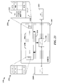
図23は、バッテリを無線で充電することを可能にする充電デバイスまたは受信デバイスに組み込むことができる装置2300のハードウェア実装の一例を示す図である。いくつかの例では、装置2300は、本明細書に開示された1または複数の機能を実行することができる。本開示の様々な態様に従って、本明細書に開示される要素、または要素の任意の部分、または要素の任意の組合せは、処理回路2302を使用して実装される。処理回路2302は、ハードウェアおよびソフトウェアモジュールのいくつかの組合せによって制御される1または複数のプロセッサ2304を含むことができる。プロセッサ2304の例には、マイクロプロセッサ、マイクロコントローラ、デジタル信号プロセッサ(DSP)、SoC、ASIC、フィールドプログラマブルゲートアレイ(FPGA)、プログラマブルロジックデバイス(PLD)、状態機械、シーケンサ、ゲートロジック、ディスクリートハードウェア回路、およびこの開示を通じて説明されている様々な機能を実行するように構成された他の適切なハードウェアが含まれる。1または複数のプロセッサ2304は、特定の機能を実行し、かつソフトウェアモジュール2316の1つにより構成、増強または制御される専用プロセッサを含むことができる。1または複数のプロセッサ2304は、初期化中にロードされるソフトウェアモジュール2316の組合せにより構成され、かつ動作中に1または複数のソフトウェアモジュール2316をロードまたはアンロードすることによってさらに構成される。
Example Processing Circuit FIG. 23 is a diagram illustrating an example hardware implementation of an
図示された例では、処理回路2302が、全体としてバス2310によって表されるバスアーキテクチャで実装される。バス2310は、処理回路2302の特定の用途および全体的な設計上の制約に応じて、任意の数の相互接続するバスおよびブリッジを含むことができる。バス2310は、1または複数のプロセッサ2304およびストレージ2306を含む様々な回路を互いにリンクする。ストレージ2306は、メモリデバイスおよび大容量ストレージデバイスを含むことができ、本明細書ではコンピュータ可読媒体および/またはプロセッサ可読媒体と呼ばれることがある。ストレージ2306は、一時的記憶媒体および/または非一時的記憶媒体を含むことができる。
In the depicted example,
また、バス2310は、タイミングソース、タイマ、周辺機器、電圧調整器および電力管理回路などの様々な他の回路をリンクすることもできる。バスインターフェース2308は、バス2310と1または複数のトランシーバ2312との間のインターフェースを提供することができる。一例では、トランシーバ2312は、装置2300が規格で規定されたプロトコルに従って充電デバイスまたは受信デバイスと通信することを可能にするために提供することができる。装置2300の特性に応じて、ユーザインターフェース2318(例えば、キーパッド、ディスプレイ、スピーカ、マイクロフォン、ジョイスティック)も提供され、直接またはバスインターフェース2308を介してバス2310に通信可能に結合されるようにしてもよい。
プロセッサ2304は、バス2310の管理を担うとともに、ストレージ2306を含むコンピュータ可読媒体に格納されたソフトウェアの実行を含む全体的な処理を担うことができる。これに関して、プロセッサ2304を含む処理回路2302は、本明細書に開示の方法、機能および手法の何れかを実行するために使用することができる。ストレージ2306は、ソフトウェアの実行時に、プロセッサ2304によって操作されるデータを記憶するために使用することができ、ソフトウェアは、本明細書に開示の方法の何れかを実行するように構成することができる。
処理回路2302内の1または複数のプロセッサ2304は、ソフトウェアを実行することができる。ソフトウェアは、ソフトウェア、ファームウェア、ミドルウェア、マイクロコード、ハードウェア記述言語などの何れかで呼ばれても、命令、命令セット、コード、コードセグメント、プログラムコード、プログラム、サブプログラム、ソフトウェアモジュール、アプリケーション、ソフトウェアアプリケーション、ソフトウェアパッケージ、ルーチン、サブルーチン、オブジェクト、実行可能ファイル、実行スレッド、プロシージャ、ファンクション、アルゴリズムなどを意味するものとして広く解釈されるものとする。ソフトウェアは、ストレージ2306または外部のコンピュータ可読媒体にコンピュータ可読形式で存在することができる。外部コンピュータ可読媒体および/またはストレージ2306は、非一時的コンピュータ可読媒体を含むことができる。非一時的コンピュータ可読媒体は、例として、磁気記憶装置(例えば、ハードディスク、フロッピーディスク、磁気ストリップ)、光ディスク(例えば、コンパクトディスク(CD)、デジタル多用途ディスク(DVD))、スマートカード、フラッシュメモリデバイス(例えば、「フラッシュドライブ」、カード、スティック、キードライブなど)、RAM、ROM、プログラマブルリードオンリーメモリ(PROM)、EEPROMを含む消去可能なPROM(EPROM)、レジスタ、リムーバブルディスク、およびコンピュータがアクセスして読み取ることができるソフトウェアおよび/または命令を格納するためのその他の適切な媒体を含むことができる。コンピュータ可読媒体および/またはストレージ2306は、例として、搬送波、伝送線、およびコンピュータがアクセスして読み取ることができるソフトウェアおよび/または命令を伝送するための任意の他の適切な媒体も含むことができる。コンピュータ可読媒体および/またはストレージ2306は、処理回路2302内、プロセッサ2304内、処理回路2302の外部に存在するか、処理回路2302を含む複数のエンティティにわたって分散配置されるものであってもよい。コンピュータ可読媒体および/またはストレージ2306は、コンピュータプログラム製品で具現化されるようにしてもよい。例として、コンピュータプログラム製品は、パッケージ材料内にコンピュータ可読媒体を含むことができる。当業者は、特定の用途およびシステム全体に課される全体的な設計上の制約に応じて、本開示全体にわたって提示および説明される機能をどのように実装するのが最善であるかを認識するであろう。
One or
ストレージ2306は、本明細書においてソフトウェアモジュール2316と呼ばれることがある、ロード可能なコードセグメント、モジュール、アプリケーション、プログラムなどで維持および/または編成されるソフトウェアを維持することができる。ソフトウェアモジュール2316の各々は、命令およびデータを含むことができ、それらは、処理回路2302にインストールまたはロードされて、1または複数のプロセッサ2304により実行されると、1または複数のプロセッサ2304の動作を制御するランタイムイメージ2314に寄与する。実行されると、特定の命令は、処理回路2302に、本明細書に記載の特定の方法、アルゴリズムおよびプロセスに従って機能を行わせることができる。
いくつかのソフトウェアモジュール2316は、処理回路2302の初期化中にロードされ、それらソフトウェアモジュール2316は、本明細書に開示の様々な機能の実行を可能にするように処理回路2302を設定することができる。例えば、いくつかのソフトウェアモジュール2316は、プロセッサ2304の内部デバイスおよび/または論理回路2322を設定し、トランシーバ2312、バスインターフェース2308、ユーザインターフェース2318、タイマ、数値演算コプロセッサなどの外部デバイスへのアクセスを管理することができる。ソフトウェアモジュール2316は、割り込みハンドラおよびデバイスドライバと相互作用し、処理回路2302によって提供される様々なリソースへのアクセスを制御する制御プログラムおよび/またはオペレーティングシステムを含むことができる。リソースは、メモリ、処理時間、トランシーバ2312へのアクセス、ユーザインターフェイス2318などを含むことができる。
A number of
処理回路2302の1または複数のプロセッサ2304は多機能であってもよく、ソフトウェアモジュール2316のいくつかが、ロードされて、異なる機能または同じ機能の異なるインスタンスを実行するように構成される。1または複数のプロセッサ2304は、例えば、ユーザインターフェース2318、トランシーバ2312およびデバイスドライバからの入力に応答して開始されるバックグラウンドタスクを管理するようにさらに適合させることができる。複数の機能の実行をサポートするために、1または複数のプロセッサ2304は、マルチタスク環境を提供するように構成され、複数の機能の各々が、必要または希望に応じて1または複数のプロセッサ2304によってサービス提供されるタスクのセットとして実装される。一例では、マルチタスク環境は、様々なタスク間でプロセッサ2304の制御を引き渡すタイムシェアリングプログラム2320を使用して実装することができ、各タスクは、未処理の動作の完了時に、かつ/または割り込みなどの入力に応答して、1または複数のプロセッサ2304の制御をタイムシェアリングプログラム2320に戻す。タスクが1または複数のプロセッサ2304の制御を有する場合、処理回路は、制御タスクに関連付けられた機能によって対処される目的のために効果的に特化される。タイムシェアリングプログラム2320は、オペレーティングシステム、ラウンドロビンベースで制御を転送するメインループ、機能の優先順位付けに従って1または複数のプロセッサ2304の制御を割り当てる機能、および/または1または複数のプロセッサ2304の制御をハンドリング機能に提供することにより、外部イベントに応答する割り込み駆動メインループを含むことができる。
One or
一実施形態では、装置2300がワイヤレス充電デバイスを含むか、またはワイヤレス充電デバイスとして動作し、ワイヤレス充電デバイスが、充電回路、複数の充電セルおよびコントローラに結合されたバッテリ充電電源を有し、コントローラが1または複数のプロセッサ2304に含まれる。複数の充電セルは、充電面を提供するように構成することができる。少なくとも1のコイルは、各充電セルの電荷伝送領域を介して電磁場を導くように構成することができる。
In one embodiment, the
コントローラは、充電回路にパルスを提供し、パルスに応答する充電回路の発振の周波数または充電回路の発振の減衰率を検出し、充電回路の特性の変化に基づいて、充電可能なデバイスが充電回路のコイルに近接して配置されたことを判定するように構成することができる。パルスは、充電回路の公称共振周波数の周期の半分未満の持続時間を有することができる。 The controller provides a pulse to the charging circuit, detects the frequency of the charging circuit's oscillations in response to the pulse or the rate of decay of the charging circuit's oscillations, and determines, based on the change in the characteristics of the charging circuit, whether the chargeable device can be configured to determine that it is placed in close proximity to the coil of the The pulse may have a duration less than half the period of the nominal resonant frequency of the charging circuit.
一例では、充電回路の特性の変化が、充電回路の発振の減衰率の変化を引き起こす。一例では、充電回路の特性の変化が、充電回路の発振の周波数の変化を引き起こし、充電回路の共振周波数に対して変化する。 In one example, changes in the characteristics of the charging circuit cause changes in the rate of decay of the oscillations of the charging circuit. In one example, a change in the characteristics of the charging circuit causes a change in the frequency of oscillation of the charging circuit, which varies with respect to the resonant frequency of the charging circuit.
特定の例では、コントローラが、充電回路のコイルが充電可能なデバイスの受信コイルに誘導的に結合されているときに、充電可能なデバイスの充電構成を決定し、その充電構成に従って充電回路に充電電流を供給するように構成されている。コントローラは、充電構成としてベースライン充電構成を選択するように構成されるものであってもよい。コントローラは、充電可能なデバイスを充電するための規格で規定された仕様に従ってアクティブpingを送信し、充電可能なデバイスから受信した変調信号にエンコードされた情報から充電可能なデバイスを識別するように構成されるものであってもよい。コントローラは、充電可能なデバイスを充電している間に使用される拡張電力プロファイルを提供するために、充電可能なデバイスと充電構成をネゴシエートするように構成されるものであってもよい。 In a particular example, the controller determines a charging configuration for the chargeable device when the coil of the charging circuit is inductively coupled to the receiving coil of the chargeable device, and charges the charging circuit according to the charging configuration. configured to supply current. The controller may be configured to select the baseline charging configuration as the charging configuration. The controller is configured to transmit an active ping according to specifications set forth in a standard for charging rechargeable devices and to identify the rechargeable device from information encoded in the modulated signal received from the rechargeable device. It may be The controller may be configured to negotiate a charging configuration with the chargeable device to provide an enhanced power profile for use while charging the chargeable device.
一例では、コントローラは、充電面の低電力探索を実行して、少なくとも1の充電コイルの電気的、機械的または磁気的特性が、少なくとも1の充電コイルの近傍に置かれた物体によって影響を受けたか否かを判定し、少なくとも1の充電コイルを含むように前記充電回路を設定するように構成されるものであってもよい。 In one example, the controller performs a low power search of the charging surface to determine if the electrical, mechanical or magnetic properties of the at least one charging coil are affected by an object placed in proximity to the at least one charging coil. and configure the charging circuit to include at least one charging coil.
一例では、コントローラは、少なくとも1の充電セルに関連付けられた静電容量の変化が、少なくとも1の充電セルに近接して配置された物体を示していることを検出し、少なくとも1の充電セルを含むように充電回路を設定するように構成されるものであってもよい。 In one example, the controller detects that the change in capacitance associated with the at least one charge cell is indicative of an object placed in close proximity to the at least one charge cell and removes the at least one charge cell. It may be configured to configure the charging circuit to include.
様々な例では、装置2300が、上部金属層と下部金属層とを有する第1のプリント回路基板を有することができ、複数の充電セルの第1の部分が第1のプリント回路基板の上部金属層上に提供され、複数の充電セルの第2の部分が第1のプリント回路基板の下部金属層上に提供される。装置2300は、上部金属層と下部金属層を有する第2のプリント回路基板を有することができ、複数の充電セルの第3の部分が第2のプリント回路基板の上部金属層上に提供され、複数の充電セルの第4の部分が第2のプリント回路基板の下部金属層上に提供される。接着剤層は、第1のプリント回路基板の下部金属層が第2のプリント回路基板の上部金属層に隣接するように、第1のプリント回路基板と第2のプリント回路基板とを接合するために使用することができる。第1のプリント回路基板の下部金属層と第2のプリント回路基板の上部金属層との間には、1または複数の相互接続部を設けることができる。
In various examples, the
別の実施形態では、ストレージ2306が、命令および情報を保持し、命令が、1または複数のプロセッサ2304に対して、充電回路にパルスを供給させ、充電回路の発振の減衰率またはパルスに応答する充電回路の発振の周波数を検出させ、充電回路の特性の変化に基づいて、充電可能なデバイスが充電回路のコイルに近接して配置されたことを判定させるように構成されている。パルスは、充電回路の公称共振周波数の周期の半分未満の持続時間を有することができる。
In another embodiment, the
一例では、充電回路の特性の変化が、充電回路の発振の減衰率の変化を引き起こする可能性がある。一実施例では、充電回路の特性の変化が、充電回路の発振の周波数を充電回路の共振周波数に対して変化させる可能性がある。 In one example, changes in the characteristics of the charging circuit can cause changes in the rate of decay of the oscillations of the charging circuit. In one example, changes in the characteristics of the charging circuit can change the frequency of oscillation of the charging circuit relative to the resonant frequency of the charging circuit.
様々な例では、命令が、1または複数のプロセッサ2304に対して、充電回路のコイルが充電可能なデバイスの受信コイルに誘導的に結合されているときに、充電可能なデバイスのための充電構成を決定させ、その充電構成に従って充電回路に充電電流を供給させるように、構成されるものであってもよい。充電可能なデバイスの充電構成は、充電構成としてベースライン充電構成を選択することにより決定されるものであってもよい。充電可能なデバイスの充電構成は、充電可能なデバイスを充電するための規格で規定された仕様に従ってアクティブPINGを送信し、充電可能なデバイスから受信した変調信号にエンコードされた情報から充電可能なデバイスを識別することによって決定されるものであってもよい。充電可能なデバイスの充電構成は、充電可能なデバイスを充電している間に使用される拡張電力プロファイルを提供するために、充電可能なデバイスと充電構成をネゴシエートすることによって決定されるものであってもよい。
In various examples, the instructions instruct one or
一例では、命令が、1または複数のプロセッサ2304に対して、複数の充電コイルの低電力探索を実行させて、少なくとも1の充電コイルの電気的、機械的または磁気的特性が、少なくとも1の充電コイルに近接して配置された物体によって影響を受けたか否かを判定させ、少なくとも1の充電コイルを含むように充電回路を設定させるように構成されるものであってもよい。
In one example, the instructions cause one or
一例では、命令が、1または複数のプロセッサ2304に対して、少なくとも1の充電コイルに関連する静電容量の変化が、少なくとも1の充電コイルに近接して配置された物体を示していることを検出させ、少なくとも1の充電コイルを含むように充電回路を設定させるように構成されるものであってもよい。
In one example, the instructions instruct one or
別の実施形態では、装置2300が、充電デバイスを含むか、または充電デバイスとして動作する。充電デバイスは、上部金属層と下部金属層とを有する第1のプリント回路基板を有することができ、第1の複数の充電セルが第1のプリント回路基板の上部金属層上に提供され、第2の複数の充電セルが第1のプリント回路基板の下部金属層上に提供される。充電デバイスは、上部金属層および下部金属層を有する第2のプリント回路基板を有することができ、第3の複数の充電セルが第2のプリント回路基板の上部金属層上に提供され、第4の複数の充電セルが第2のプリント回路基板の下部金属層上に提供される。接着剤層は、第1のプリント回路基板の下部金属層が第2のプリント回路基板の上部金属層に隣接するように、第1のプリント回路基板と第2のプリント回路基板とを接合することができる。第1のプリント回路基板の下部金属層と第2のプリント回路基板の上部金属層との間には、1または複数の相互接続部を設けることができる。いくつかの実施例では、第1の複数の充電セル、第2の複数の充電セル、第3の複数の充電セルおよび第4の複数の充電セルのうちの各充電セルが、充電デバイスに設けられた他の充電セルとは独立して通電されるようにしてもよい。
In another embodiment,
一実施例では、第1のプリント回路基板および第2のプリント回路基板の少なくとも一方が、上部金属層と下部金属層との間に設けられた1または複数の内部金属層を有する。追加の充電セルを、1または複数の内部金属層上に提供することができる。 In one embodiment, at least one of the first printed circuit board and the second printed circuit board has one or more inner metal layers disposed between upper and lower metal layers. Additional charge cells can be provided on one or more of the inner metal layers.
特定の実施例では、第1のプリント回路基板および第2のプリント回路基板が、充電されるデバイスに充電面を提供する。第1の複数の充電セル、第2の複数の充電セル、第3の複数の充電セルおよび第4の複数の充電セルのうちの各充電セルは、充電面に関連付けられた電力伝送領域の一部を取り囲むコイルを有することができる。充電面は、第1のプリント回路基板の上部金属層に対応し得る。スイッチのセットは、充電デバイスの少なくとも1の充電セルを電源に選択的に結合するように動作可能であってもよく、コントローラは、充電面に対する充電されるデバイスの向きまたは位置に基づいて、少なくとも1の充電セルを選択するように構成されるものであってもよい。検出回路は、少なくとも1のプリント回路基板の少なくとも1の層上の充電セルに結合されるものであってもよく、検出回路は、2以上の充電セルに関連する静電容量の差を検出するように構成されている。 In certain embodiments, the first printed circuit board and the second printed circuit board provide charging surfaces for the device being charged. Each charge cell of the first plurality of charge cells, the second plurality of charge cells, the third plurality of charge cells and the fourth plurality of charge cells has a power transfer region associated with the charge surface. It can have a coil surrounding the portion. The charging surface may correspond to the top metal layer of the first printed circuit board. The set of switches may be operable to selectively couple at least one charge cell of the charging device to the power source, and the controller determines at least It may be configured to select one charge cell. A detection circuit may be coupled to the charge cells on at least one layer of the at least one printed circuit board, the detection circuit detecting a difference in capacitance associated with the two or more charge cells. is configured as
コントローラは、静電容量の差に基づいて少なくとも1の充電セルを選択するようにさらに構成されるものであってもよい。コントローラは、静電容量の差に基づいて、少なくとも1の充電セルに供給される電流の極性およびレベルを選択するようにさらに構成されるものであってもよい。コントローラは、2以上の充電セルに関連付けられた静電容量の差の変化を測定し、静電容量の差の変化に基づいて、少なくとも1の充電セルに供給される電流の極性またはレベルを変更するようにさらに構成されるものであってもよい。コントローラは、静電容量の差に基づいて、充電されるデバイスの向きまたは位置を判定するようにさらに構成されるものであってもよい。コントローラは、充電セルのシーケンスの各充電セルで測定された静電容量を求めることにより、充電されるべきデバイスを定期的に探索するようにさらに構成されるものであってもよい。充電セルのシーケンスは、連続する探索の間に疑似ランダムに生成されるものであってもよい。コントローラは、充電されるデバイスの開始点を選択するようにさらに構成されるものであってもよい。 The controller may be further configured to select the at least one charge cell based on the capacitance difference. The controller may be further configured to select the polarity and level of current supplied to the at least one charge cell based on the capacitance difference. The controller measures a change in the difference in capacitance associated with the two or more charge cells and changes the polarity or level of current supplied to at least one charge cell based on the change in the difference in capacitance. It may be further configured to. The controller may be further configured to determine the orientation or position of the device being charged based on the difference in capacitance. The controller may be further configured to periodically search for devices to be charged by determining the measured capacitance of each charge cell of the sequence of charge cells. The sequence of charge cells may be pseudo-randomly generated during successive searches. The controller may be further configured to select a starting point for the device to be charged.
一例では、少なくとも1の相互接続部が、第1のプリント回路基板の上部金属層を貫通しない。一例では、少なくとも1つの相互接続部が、第2のプリント回路基板の下部金属層を貫通しない。一例では、接着剤層が開口部を含み、この開口部を通って、少なくとも1つの相互接続部が第1のプリント回路基板と第2のプリント回路基板との間を通過する。一例では、第1のプリント回路基板および第2のプリント回路基板の各々が、フレキシブルプリント回路基板を有する。一例では、第1のプリント回路基板および第2のプリント回路基板の各々が、非平面プリント回路基板を有する。 In one example, at least one interconnect does not penetrate the top metal layer of the first printed circuit board. In one example, at least one interconnect does not penetrate the bottom metal layer of the second printed circuit board. In one example, the adhesive layer includes an opening through which at least one interconnect passes between the first printed circuit board and the second printed circuit board. In one example, the first printed circuit board and the second printed circuit board each comprise a flexible printed circuit board. In one example, the first printed circuit board and the second printed circuit board each have a non-planar printed circuit board.
別の実施形態では、装置2300が、フレキシブル回路がバッテリに取り付けられたときに、少なくとも2つの軸に沿って電力伝送領域を提供するように構成された複数のコイルを含むフレキシブル回路と、バッテリに電気的に結合された電力管理回路とを有する。電力管理回路は、バッテリの充電レベルを測定し、ワイヤレス充電源から無線で伝送された電力を受信し、さらに、バッテリの充電レベルが最大閾値充電レベル以下であって、かつワイヤレス充電源が複数のコイルのうちの1または複数を介して電力を送信しているときに、バッテリに充電電流を供給するように構成または適合されるものであってもよい。
In another embodiment, the
一例では、少なくとも2つの軸が、バッテリの表面上の一対の直行軸を含む。フレキシブル回路は、バッテリの少なくとも一部を包囲することができる。一例では、フレキシブル回路が、電磁シールドを提供するように構成されたシート材料を含む。シート材料は、フレキシブル回路がバッテリの周りに巻かれたときに、複数のコイルとバッテリとの間に配置されるものであってもよい。一例では、複数のコイルが、フレキシブル回路の少なくとも4の金属層に形成されている。 In one example, the at least two axes include a pair of orthogonal axes on the surface of the battery. A flexible circuit can surround at least a portion of the battery. In one example, a flexible circuit includes a sheet material configured to provide electromagnetic shielding. A sheet of material may be disposed between the plurality of coils and the battery when the flexible circuit is wrapped around the battery. In one example, multiple coils are formed in at least four metal layers of a flexible circuit.
上述した説明は、当業者が本明細書に記載の様々な態様を実施できるようにするために提供されたものである。これらの態様に対する様々な変更は、当業者にはすぐに明らかであり、本明細書で規定される一般的な原理は、他の態様に適用することができる。このため、特許請求の範囲は、本明細書に示される態様に限定されることを意図するものではなく、請求項の文言と一致する全範囲が認められるものであり、単数形の要素への言及は、特に明記がなければ、「唯一の」を意味するものではなく、「1または複数」を意味するものとする。特に明記されていない限り、「いくつか」という用語は1または複数を指す。当業者に知られている、または後に当業者に知られるようになる、本開示を通して説明される様々な態様の要素に対するすべての構造的および機能的均等物は、引用により本明細書に明示的に援用されるとともに、特許請求の範囲に含まれることが意図される。さらに、本明細書に開示されているものは、そのような開示が特許請求の範囲に明示的に記載されているか否かにかかわらず、公衆に捧げられることを意図していない。請求項の要素が「のための手段(means for)」という文言を使用して明示的に記載されていない限り、また、方法の請求項の場合には、「のためのステップ(step for)」という文言を使用して記載されていない限りは、何れの請求項の要素も、米国特許法第112条第6段落の規定に基づいて解釈されるべきではない。
The previous description is provided to enable any person skilled in the art to practice the various aspects described herein. Various modifications to these aspects will be readily apparent to those skilled in the art, and the general principles defined herein may be applied to other aspects. For this reason, the claims are not intended to be limited to the aspects shown herein, but are to be accorded full scope consistent with the language of the claims, revising to elements in the singular. References shall mean "one or more" rather than "only" unless otherwise specified. Unless otherwise specified, the term "some" refers to one or more. All structural and functional equivalents to the elements of the various embodiments described throughout this disclosure that are known or later become known to those of skill in the art are expressly incorporated herein by reference. and is intended to be included in the claims. Moreover, nothing disclosed herein is intended to be dedicated to the public, whether or not such disclosure is explicitly recited in the claims. Unless a claim element is explicitly recited using the language "means for," and in the case of a method claim, a "step for No claim element should be construed under the provisions of 35 U.S.C.
Claims (24)
ワイヤレス充電デバイスの充電面を探索するステップであって、
前記充電面内の複数の電力送信コイルにパルスを供給するステップであって、各パルスが、充電回路の公称共振周波数の周期の半分未満の持続時間を有しており、各パルスが、前記電力送信コイルに接続された前記充電回路の発振を引き起こすように構成されている、パルスを供給するステップと、
前記充電回路の発振の減衰率または前記充電回路の発振の周波数を検出するステップと、
対応する充電回路の前記発振の減衰率または前記発振の周波数に基づいて、前記複数の電力送信コイルの1つ以上が、1つ以上の充電可能なデバイスの近傍に配置されているかどうかを判定するステップと、を含む充電面を探索するステップと、
前記充電面を探索するステップの間、1つ以上の前記電力送信コイルが1つ以上の前記充電可能なデバイスの近傍に配置されていると判定された時に、ワイヤレス充電の規格で規定された仕様に従って、前記複数の電力送信コイルの1つ以上にデジタルpingを送信するステップと、
1つ以上の前記充電可能なデバイスに送信された前記デジタルpingに応答して、1つ以上の前記充電可能なデバイスから受信した変調信号にエンコードされた情報に基づいて、1つ以上の前記充電可能なデバイスの充電構成を決定するステップと、を備えることを特徴とする方法。 In a method of detecting an object,
probing a charging surface of a wireless charging device, comprising:
supplying pulses to a plurality of power transmitting coils in the charging plane, each pulse having a duration less than half the period of the nominal resonant frequency of the charging circuit, each pulse providing a pulse configured to cause oscillation of the charging circuit connected to a transmitting coil;
detecting a decay rate of oscillation of the charging circuit or a frequency of oscillation of the charging circuit;
Determining whether one or more of the plurality of power transmit coils are positioned in proximity to one or more chargeable devices based on a decay rate of the oscillations or a frequency of the oscillations of corresponding charging circuits. searching for a charging surface comprising;
Specifications defined in standards for wireless charging when it is determined that one or more of the power transmitting coils are positioned in proximity to one or more of the chargeable devices during the step of searching the charging surface. sending a digital ping to one or more of the plurality of power transmit coils according to;
one or more of the rechargeable devices based on information encoded in modulated signals received from one or more of the rechargeable devices in response to the digital pings sent to one or more of the rechargeable devices. determining possible device charging configurations.
前記充電面を探索するステップの間の第1の電力送信コイルの発振の減衰率が、前記第1の電力送信コイルの前に検出された発振の減衰率と異なる時に、前記第1の電力送信コイルが充電装置の近傍にあると判定することを特徴とする方法。 The method of claim 1, wherein
the first power transmission when the decay rate of oscillations of the first power transmission coil during the step of searching the charging surface is different than the decay rate of previously detected oscillations of the first power transmission coil; A method comprising determining that the coil is in the vicinity of the charging device.
前記充電面を探索するステップの間の第2の電力送信コイルの発振の減衰率が、前記第2の電力送信コイルの前に検出された発振の減衰率と異なる時に、前記第2の電力送信コイルが充電装置の近傍にあると判定することを特徴とする方法。 The method of claim 1, wherein
the second power transmission when the decay rate of the oscillation of the second power transmit coil during the step of searching the charging surface is different from the decay rate of the previously detected oscillation of the second power transmit coil; A method comprising determining that the coil is in the vicinity of the charging device.
2つの電力送信コイルが1つ以上の前記充電可能な装置の近傍にあると判定された時に、前記充電構成を決定するステップと、
前記充電構成に従って、第1の電力送信コイルおよび第2の電力送信コイルに充電電流を供給するステップと、を備えることを特徴とする方法。 The method of claim 1, further comprising:
determining the charging configuration when two power transmitting coils are determined to be in proximity to one or more of the rechargeable devices;
and C. supplying a charging current to a first power transmitting coil and a second power transmitting coil according to the charging configuration .
1つ以上の前記充電可能なデバイスの充電構成を決定するステップが、
前記充電構成としてベースライン充電構成を選択するステップを含むことを特徴とする方法。 The method of claim 1, wherein
determining a charging configuration for one or more of the rechargeable devices;
A method, comprising: selecting a baseline charging configuration as the charging configuration.
1つ以上の前記充電可能なデバイスの充電構成を決定するステップが、
1つ以上の前記充電可能なデバイスと前記充電構成をネゴシエートして、1つ以上の前記充電可能なデバイスの充電中に使用される拡張電力プロファイルを提供するステップを含むことを特徴とする方法。 The method of claim 1, wherein
determining a charging configuration for one or more of the rechargeable devices;
negotiating the charging configuration with one or more of the rechargeable devices to provide an enhanced power profile for use during charging of one or more of the rechargeable devices.
前記充電面の低電力探索を実行して、少なくとも1つの前記電力送信コイルの電気的、機械的または磁気的特性が、少なくとも1つの前記電力送信コイルの近傍に置かれた物体によって影響を受けているかどうかを判定するステップと、
前記充電面を探索するステップの際に、パルスが供給された前記複数の電力送信コイルに前記少なくとも1つの電力送信コイルを含ませるステップと、を含むことを特徴とする方法。 The method of claim 1, further comprising:
performing a low-power search of the charging surface such that electrical, mechanical or magnetic properties of at least one of the power transmitting coils are affected by an object placed in proximity to the at least one power transmitting coil determining whether there is
and c. including the at least one power transmitting coil in the plurality of pulsed power transmitting coils during the step of searching the charging surface.
少なくとも1つの前記電力送信コイルの近傍に物体が配置されていることを示す、少なくとも1つの前記電力送信コイルに関する静電容量の変化を検出するステップと、
前記充電面を探索するステップの際に、パルスが供給された前記複数の電力送信コイルに前記少なくとも1つの電力送信コイルを含ませるステップと、を含むことを特徴とする方法。 The method of claim 1, further comprising:
detecting a change in capacitance with respect to at least one of said power transmission coils indicative of an object being placed in the vicinity of said at least one of said power transmission coils;
and c. including the at least one power transmitting coil in the plurality of pulsed power transmitting coils during the step of searching the charging surface.
充電回路に結合されたバッテリ充電電源と、
充電面を提供するように構成された複数の充電セルであって、前記充電面内の1つ以上の電力送信コイルが、各充電セルの電荷伝送領域を介して電磁場を誘導するように構成されている、複数の充電セルと、
コントローラとを備え、当該コントローラが、
前記充電面内の1つ以上の電力送信コイルにパルスを供給するステップであって、各パルスが、充電回路の公称共振周波数の周期の半分未満の持続時間を有しており、各パルスが、1つ以上の電力送信コイルに接続された前記充電回路の発振を引き起こすように構成されている、パルスを供給するステップと、
前記充電回路の発振の減衰率または前記充電回路の発振の周波数を検出するステップと、
対応する充電回路の前記発振の減衰率または前記発振の周波数に基づいて、1つ以上の電力送信コイルのそれぞれが、1つ以上の充電可能なデバイスの近傍に配置されているかどうかを判定するステップと、を実行して充電面を探索し、
前記充電面を探索する間、1つ以上の前記電力送信コイルが1つ以上の前記充電可能なデバイスの近傍に配置されていると判定された時に、ワイヤレス充電の規格で規定された仕様に従って、前記1つ以上の電力送信コイルの1つ以上にデジタルpingを送信し、
1つ以上の前記充電可能なデバイスに送信された前記デジタルpingに応答して、1つ以上の前記充電可能なデバイスから受信した変調信号にエンコードされた情報に基づいて、1つ以上の前記充電可能なデバイスの充電構成を決定する、ように構成されていることを特徴とするワイヤレス充電デバイス。 In wireless charging devices,
a battery charging power supply coupled to the charging circuit;
A plurality of charge cells configured to provide a charge surface, wherein one or more power transmission coils within the charge surface are configured to induce an electromagnetic field through a charge transfer region of each charge cell. a plurality of charge cells,
a controller, the controller comprising:
supplying pulses to one or more power transmitting coils in the charging plane, each pulse having a duration less than half the period of the nominal resonant frequency of the charging circuit, each pulse comprising: providing a pulse configured to cause oscillation of the charging circuit connected to one or more power transmission coils;
detecting a decay rate of oscillation of the charging circuit or a frequency of oscillation of the charging circuit;
Determining whether each of the one or more power transmitting coils is positioned in proximity to one or more chargeable devices based on the decay rate of said oscillations or the frequency of said oscillations of the corresponding charging circuit. , to explore the charging surface,
When it is determined that one or more of the power transmitting coils are located in proximity to one or more of the chargeable devices while probing the charging surface, according to specifications set forth in wireless charging standards, sending a digital ping to one or more of the one or more power transmit coils;
one or more of the rechargeable devices based on information encoded in modulated signals received from one or more of the rechargeable devices in response to the digital pings sent to one or more of the rechargeable devices. A wireless charging device configured to determine possible device charging configurations.
前記充電面を探索する間の第1の電力送信コイルの発振の減衰率が、前記第1の電力送信コイルの前に検出された発振の減衰率と異なる時に、前記第1の電力送信コイルが充電装置の近傍にあると判定することを特徴とするワイヤレス充電デバイス。 A wireless charging device according to claim 9, wherein
when the decay rate of the oscillation of the first power transmit coil while searching the charging surface is different from the decay rate of the previously detected oscillation of the first power transmit coil, the first power transmit coil A wireless charging device that determines that it is in the vicinity of a charging device.
前記充電面を探索する間の第2の電力送信コイルの発振の減衰率が、前記第2の電力送信コイルの前に検出された発振の減衰率と異なる時に、前記第2の電力送信コイルが充電装置の近傍にあると判定することを特徴とするワイヤレス充電デバイス。 A wireless charging device according to claim 9, wherein
when the decay rate of the oscillation of the second power transmit coil while searching the charging surface is different from the decay rate of the oscillation detected before the second power transmit coil, the second power transmit coil A wireless charging device that determines that it is in the vicinity of a charging device.
前記コントローラが、
2つの電力送信コイルが少なくとも1つの前記充電可能な装置の近傍にあると判定された時に、前記充電構成を決定し、
前記充電構成に従って、第1の電力送信コイルおよび第2の電力送信コイルに充電電流を供給する、ように構成されていることを特徴とするワイヤレス充電デバイス。 A wireless charging device according to claim 9, wherein
the controller
determining the charging configuration when two power transmitting coils are determined to be in proximity to at least one of the rechargeable devices;
A wireless charging device configured to supply charging current to a first power transmitting coil and a second power transmitting coil according to the charging configuration .
前記コントローラが、前記充電構成としてベースライン充電構成を選択するように構成されていることを特徴とするワイヤレス充電デバイス。 A wireless charging device according to claim 9, wherein
A wireless charging device, wherein the controller is configured to select a baseline charging configuration as the charging configuration.
前記コントローラが、1つ以上の前記充電可能なデバイスと前記充電構成をネゴシエートして、1つ以上の前記充電可能なデバイスの充電中に使用される拡張電力プロファイルを提供するように構成されていることを特徴とするワイヤレス充電デバイス。 A wireless charging device according to claim 9, wherein
The controller is configured to negotiate the charging configuration with one or more of the rechargeable devices to provide an enhanced power profile for use during charging of one or more of the rechargeable devices. A wireless charging device characterized by:
前記コントローラが、
前記充電面の低電力探索を実行して、少なくとも1つの前記電力送信コイルの電気的、機械的または磁気的特性が、少なくとも1つの前記充電セルの近傍に置かれた物体によって影響を受けているかどうかを判定し、
前記充電面を探索する際に、パルスが供給された複数の前記電力送信コイルに前記少なくとも1つの電力送信コイルを含ませる、ように構成されていることを特徴とするワイヤレス充電デバイス。 A wireless charging device according to claim 9, wherein
the controller
performing a low power search of the charging surface to see if the electrical, mechanical or magnetic properties of at least one of the power transmitting coils have been affected by an object placed in the vicinity of at least one of the charging cells; determine what
A wireless charging device configured to include said at least one power transmitting coil in a plurality of said power transmitting coils being pulsed when searching said charging surface.
前記コントローラが、
少なくとも1つの前記電力送信コイルの近傍に物体が配置されていることを示す、少なくとも1つの前記電力送信コイルに関する静電容量の変化を検出し、
前記充電面を探索する際に、パルスが供給された前記複数の電力送信コイルに前記少なくとも1つの電力送信コイルを含ませる、ように構成されていることを特徴とするワイヤレス充電デバイス。 A wireless charging device according to claim 9, wherein
the controller
detecting a change in capacitance for at least one of the power transmission coils indicative of an object being placed in proximity to the at least one power transmission coil;
A wireless charging device configured to cause said plurality of pulsed power transmitting coils to include said at least one power transmitting coil when searching said charging surface.
上部金属層および下部金属層を有する第1のプリント回路基板であって、複数の充電セルの第1の部分が第1のプリント回路基板の上部金属層上に提供され、複数の充電セルの第2の部分が第1のプリント回路基板の下部金属層上に提供されている、第1のプリント回路基板と、
上部金属層および下部金属層を有する第2のプリント回路基板であって、複数の充電セルの第3の部分が第2のプリント回路基板の上部金属層上に提供され、複数の充電セルの第4の部分が第2のプリント回路基板の下部金属層上に提供されている、第2のプリント回路基板と、
前記第1のプリント回路基板の下部金属層が前記第2のプリント回路基板の上部金属層に隣接するように、前記第1のプリント回路基板と前記第2のプリント回路基板とを接合する接着剤層と、を備えることを特徴とするワイヤレス充電デバイス。 The wireless charging device of claim 9, further comprising:
A first printed circuit board having an upper metal layer and a lower metal layer, wherein a first portion of a plurality of charge cells is provided on the upper metal layer of the first printed circuit board, and a first portion of the plurality of charge cells is provided on the upper metal layer of the first printed circuit board. a first printed circuit board having two portions provided on a lower metal layer of the first printed circuit board;
A second printed circuit board having an upper metal layer and a lower metal layer, wherein a third portion of the plurality of charge cells is provided on the upper metal layer of the second printed circuit board and a third portion of the plurality of charge cells is provided on the upper metal layer of the second printed circuit board. a second printed circuit board, wherein four portions are provided on the lower metal layer of the second printed circuit board;
an adhesive bonding the first printed circuit board and the second printed circuit board such that the bottom metal layer of the first printed circuit board is adjacent to the top metal layer of the second printed circuit board; A wireless charging device comprising: a layer;
前記第1のプリント回路基板の下部金属層と前記第2のプリント回路基板の上部金属層との間に設けられた1または複数の相互接続部を備えることを特徴とするワイヤレス充電デバイス。 18. The wireless charging device of claim 17, further comprising one or more interconnects between a bottom metal layer of the first printed circuit board and a top metal layer of the second printed circuit board. A wireless charging device, comprising:
第1の充電コイルに第1のパルスを供給するステップであって、前記第1の充電コイルが、充電面にわたって設けられた複数の充電コイルのうちの1つであり、前記第1のパルスが、前記第1の充電コイルを含む第1の充電回路の発振を引き起こすように構成されている、第1のパルスを供給するステップと、
第2の充電コイルに第2のパルスを供給するステップであって、前記第2の充電コイルが、充電面にわたって設けられた複数の充電コイルのうちの1つであり、前記第2のパルスが、前記第2の充電コイルを含む第2の充電回路の発振を引き起こすように構成されている、第2のパルスを供給するステップと、
前記第1のパルスおよび前記第2のパルスに対する前記第1の充電回路および前記第2の充電回路の応答を検出するステップであって、前記応答が、発振の減衰率または発振の周波数に関するものであるステップと、
前記応答が、充電可能なデバイスが前記第1の充電コイルまたは前記第2の充電コイルの近傍に配置されていることを示した時に、前記応答を使用して、前記第1の充電コイルおよび前記第2の充電コイルを選択して送信コイルとして機能させるステップと、
前記第1のパルスおよび前記第2のパルスが、前記第1の充電回路または前記第2の充電回路に関する公称共振周波数の周期の半分未満の持続時間を有する時に、前記送信コイルを通してアクティブpingを送信するステップと、を備えることを特徴とする方法。 In the method of identifying a chargeable device,
applying a first pulse to a first charging coil, wherein the first charging coil is one of a plurality of charging coils disposed across a charging surface; , providing a first pulse configured to cause oscillation of a first charging circuit including the first charging coil;
applying a second pulse to a second charging coil, said second charging coil being one of a plurality of charging coils disposed across a charging surface, said second pulse , providing a second pulse configured to cause oscillation of a second charging circuit including the second charging coil;
detecting the response of said first charging circuit and said second charging circuit to said first pulse and said second pulse, said response relating to a decay rate of oscillation or a frequency of oscillation; a step and
Using the response to charge the first charging coil and the selecting a second charging coil to function as a transmitting coil;
Sending an active ping through the transmit coil when the first pulse and the second pulse have a duration less than half the period of the nominal resonant frequency for the first charging circuit or the second charging circuit. and a method.
前記第1の充電コイルおよび前記第2の充電コイルを含む複数の充電コイルの各々に関する静電容量を経時的に測定するステップであって、静電容量測定の経時的な順番が、静電容量測定の履歴に基づいた開始点から開始される擬似ランダム探索パターンに基づくものであるステップと、
前記第1の充電コイルまたは前記第2の充電コイルに関する静電容量の変化を検出するステップであって、当該静電容量の変化は前記充電面の近傍に物体が配置されていることを示しており、前記第1の充電コイルまたは前記第2の充電コイルに関する静電容量の変化の検出に基づいて、前記第1のパルスおよび前記第2のパルスが送信されるものであるステップと、を備えることを特徴とする方法。 20. The method of claim 19, further comprising:
measuring over time a capacitance for each of a plurality of charging coils including the first charging coil and the second charging coil, wherein the temporal order of the capacitance measurements is the capacitance is based on a pseudo-random search pattern starting from a starting point based on a history of measurements;
detecting a change in capacitance for the first charging coil or the second charging coil, wherein the change in capacitance is indicative of an object being placed in proximity to the charging surface; and wherein the first and second pulses are transmitted based on detection of a change in capacitance for the first charging coil or the second charging coil. A method characterized by:
前記アクティブpingに対する前記充電可能なデバイスの応答に基づいて、前記充電可能なデバイスを構成するステップを備えることを特徴とする方法。 20. The method of claim 19, further comprising:
A method comprising configuring the rechargeable device based on the rechargeable device's response to the active ping.
前記充電可能なデバイスを構成するステップが、
前記アクティブpingに応答して前記充電可能なデバイスから受信した変調信号にエンコードされた情報に基づいて、前記充電可能なデバイスの充電構成を決定するステップと、
前記充電構成に従って、前記第1の充電回路および前記第2の充電回路に充電電流を供給するステップと、を含むことを特徴とする方法。 20. The method of claim 19, wherein
Configuring the rechargeable device comprises:
determining a charging configuration for the rechargeable device based on information encoded in a modulated signal received from the rechargeable device in response to the active ping;
and C. supplying charging current to the first charging circuit and the second charging circuit according to the charging configuration.
前記充電可能なデバイスの充電構成を決定するステップが、
前記充電構成としてベースライン充電構成を選択するステップを含むことを特徴とする方法。 23. The method of claim 22, wherein
determining a charging configuration for the rechargeable device comprising:
A method, comprising: selecting a baseline charging configuration as the charging configuration.
前記充電可能なデバイスの充電構成を決定するステップが、
前記充電可能なデバイスと前記充電構成をネゴシエートして、前記充電可能なデバイスの充電中に使用される拡張電力プロファイルを提供するステップを含むことを特徴とする方法。 23. The method of claim 22, wherein
determining a charging configuration for the rechargeable device comprising:
negotiating the charging configuration with the rechargeable device to provide an enhanced power profile to be used while charging the rechargeable device.
Priority Applications (2)
| Application Number | Priority Date | Filing Date | Title |
|---|---|---|---|
| JP2022141905A JP2022177084A (en) | 2018-02-23 | 2022-09-07 | Free positioning charging pad |
| JP2022141904A JP2022177083A (en) | 2018-02-23 | 2022-09-07 | Free positioning charging pad |
Applications Claiming Priority (9)
| Application Number | Priority Date | Filing Date | Title |
|---|---|---|---|
| US201862634799P | 2018-02-23 | 2018-02-23 | |
| US62/634,799 | 2018-02-23 | ||
| US201862784667P | 2018-12-24 | 2018-12-24 | |
| US62/784,667 | 2018-12-24 | ||
| US201962794541P | 2019-01-18 | 2019-01-18 | |
| US62/794,541 | 2019-01-18 | ||
| US16/283,734 US11171502B2 (en) | 2018-02-23 | 2019-02-22 | Free positioning charging pad |
| US16/283,734 | 2019-02-22 | ||
| PCT/US2019/019457 WO2019165383A1 (en) | 2018-02-23 | 2019-02-25 | Free positioning charging pad |
Related Child Applications (2)
| Application Number | Title | Priority Date | Filing Date |
|---|---|---|---|
| JP2022141904A Division JP2022177083A (en) | 2018-02-23 | 2022-09-07 | Free positioning charging pad |
| JP2022141905A Division JP2022177084A (en) | 2018-02-23 | 2022-09-07 | Free positioning charging pad |
Publications (3)
| Publication Number | Publication Date |
|---|---|
| JP2021515513A JP2021515513A (en) | 2021-06-17 |
| JPWO2019165383A5 JPWO2019165383A5 (en) | 2022-03-09 |
| JP7142962B2 true JP7142962B2 (en) | 2022-09-28 |
Family
ID=67686201
Family Applications (3)
| Application Number | Title | Priority Date | Filing Date |
|---|---|---|---|
| JP2020544282A Active JP7142962B2 (en) | 2018-02-23 | 2019-02-25 | Free position charging pad |
| JP2022141904A Pending JP2022177083A (en) | 2018-02-23 | 2022-09-07 | Free positioning charging pad |
| JP2022141905A Pending JP2022177084A (en) | 2018-02-23 | 2022-09-07 | Free positioning charging pad |
Family Applications After (2)
| Application Number | Title | Priority Date | Filing Date |
|---|---|---|---|
| JP2022141904A Pending JP2022177083A (en) | 2018-02-23 | 2022-09-07 | Free positioning charging pad |
| JP2022141905A Pending JP2022177084A (en) | 2018-02-23 | 2022-09-07 | Free positioning charging pad |
Country Status (6)
| Country | Link |
|---|---|
| US (4) | US11171502B2 (en) |
| EP (1) | EP3756264A4 (en) |
| JP (3) | JP7142962B2 (en) |
| KR (1) | KR20200124242A (en) |
| CN (1) | CN111758202A (en) |
| WO (1) | WO2019165383A1 (en) |
Families Citing this family (30)
| Publication number | Priority date | Publication date | Assignee | Title |
|---|---|---|---|---|
| US11183866B2 (en) * | 2018-04-09 | 2021-11-23 | CTOP Wireless Charging Solutions LLC | System and method for switchable multi-coil wireless induction charging |
| US10594368B1 (en) * | 2019-01-31 | 2020-03-17 | Capital One Services, Llc | Array and method for improved wireless communication |
| US11063480B2 (en) * | 2019-05-28 | 2021-07-13 | Aira, Inc. | Adaptive passive Ping |
| WO2021045780A1 (en) * | 2019-09-06 | 2021-03-11 | Google Llc | Wireless charging using time-division multiplexing |
| CN112803600A (en) * | 2019-11-14 | 2021-05-14 | Oppo广东移动通信有限公司 | Wireless charging receiving end equipment, transmitting end equipment and wireless charging system |
| US20210152034A1 (en) * | 2019-11-20 | 2021-05-20 | Aira Inc. | Free-Position Wireless Charger Keep-Out |
| US11728689B2 (en) * | 2019-11-20 | 2023-08-15 | Aira, Inc. | Stacked printed circuit board surface in a free-position wireless charger |
| CN111162521B (en) * | 2019-12-31 | 2022-10-25 | 联想(北京)有限公司 | Power supply equipment and power supply method |
| US11469041B2 (en) * | 2020-01-06 | 2022-10-11 | Aira, Inc. | Dynamic multi-coil tuning |
| US11837882B2 (en) * | 2020-01-06 | 2023-12-05 | Aira, Inc. | Amplitude shift key modulation for multi-device wireless chargers |
| US11837883B2 (en) * | 2020-01-21 | 2023-12-05 | Aira, Inc. | Multi-coil wireless charger validation |
| US20210249911A1 (en) * | 2020-02-06 | 2021-08-12 | Aira, Inc. | Modular free-positioning wireless charging devices |
| KR20210101705A (en) * | 2020-02-10 | 2021-08-19 | 삼성전자주식회사 | Method for wireless charging and electronic device supporting the same |
| CN113555979A (en) * | 2020-04-24 | 2021-10-26 | 北京小米移动软件有限公司 | Wireless charging positioning device, method and storage medium |
| KR20210133064A (en) * | 2020-04-28 | 2021-11-05 | 삼성전자주식회사 | Wireless power transmission and control method thereof |
| US11462944B2 (en) | 2020-06-04 | 2022-10-04 | Aira, Inc. | Resonant class D wireless transmitter |
| US11398752B2 (en) | 2020-06-04 | 2022-07-26 | Aira, Inc. | Zero-crossing slotted foreign object detection |
| US11462945B2 (en) * | 2020-06-04 | 2022-10-04 | Aira, Inc. | Zero-crossing amplitude shift keying demodulation |
| US20220051065A1 (en) * | 2020-08-13 | 2022-02-17 | Aira, Inc. | Radio frequency identification for multi-device wireless chargers |
| US20220052565A1 (en) * | 2020-08-15 | 2022-02-17 | Aira, Inc. | Resonant Reflection Device Detection |
| US20220052556A1 (en) * | 2020-08-16 | 2022-02-17 | Aira, Inc. | Digital Ping Selection In A Multi-Coil Wireless Charging Device |
| US20220052561A1 (en) * | 2020-08-16 | 2022-02-17 | Aira, Inc. | Adaptive Foreign Object Detection Avoidance In A Multi-Coil Wireless Charging Device |
| US11496001B2 (en) * | 2020-09-08 | 2022-11-08 | Powermat Technologies Ltd. | Detection of foreign object and friendly metal |
| US20220109334A1 (en) * | 2020-10-01 | 2022-04-07 | Aira, Inc. | Digital ping clamp ramp |
| US11637441B2 (en) | 2020-11-02 | 2023-04-25 | Aira, Inc. | Thermal regulation for wireless charging pad |
| CN112902829B (en) * | 2021-01-21 | 2023-06-09 | 维沃移动通信有限公司 | Electronic equipment and opening and closing angle detection method thereof |
| US20220247228A1 (en) * | 2021-02-03 | 2022-08-04 | Aira, Inc. | Automotive key fob interference prevention in wireless chargers |
| US20220271570A1 (en) * | 2021-02-24 | 2022-08-25 | Aira, Inc. | Integrated transmitter-transformer for wireless charging |
| CN113257046B (en) * | 2021-04-07 | 2023-05-09 | 顺德职业技术学院 | Power supply base for teaching equipment |
| US11936211B2 (en) * | 2021-05-05 | 2024-03-19 | Aira, Inc. | Mixed analog front-end for wireless charging |
Citations (2)
| Publication number | Priority date | Publication date | Assignee | Title |
|---|---|---|---|---|
| JP2013031315A (en) | 2011-07-29 | 2013-02-07 | Toko Inc | Wireless power transmission equipment and relative position detection method |
| JP2017520223A (en) | 2014-06-19 | 2017-07-20 | コーニンクレッカ フィリップス エヌ ヴェKoninklijke Philips N.V. | Wireless inductive power transmission |
Family Cites Families (39)
| Publication number | Priority date | Publication date | Assignee | Title |
|---|---|---|---|---|
| US7902842B2 (en) * | 2005-06-03 | 2011-03-08 | Synaptics Incorporated | Methods and systems for switched charge transfer capacitance measuring using shared components |
| US7952322B2 (en) | 2006-01-31 | 2011-05-31 | Mojo Mobility, Inc. | Inductive power source and charging system |
| US8169185B2 (en) | 2006-01-31 | 2012-05-01 | Mojo Mobility, Inc. | System and method for inductive charging of portable devices |
| US11201500B2 (en) * | 2006-01-31 | 2021-12-14 | Mojo Mobility, Inc. | Efficiencies and flexibilities in inductive (wireless) charging |
| US11329511B2 (en) * | 2006-06-01 | 2022-05-10 | Mojo Mobility Inc. | Power source, charging system, and inductive receiver for mobile devices |
| US7948208B2 (en) * | 2006-06-01 | 2011-05-24 | Mojo Mobility, Inc. | Power source, charging system, and inductive receiver for mobile devices |
| US7266470B1 (en) | 2007-01-17 | 2007-09-04 | Eaton Corporation | Method for mitigating interference between nearby proximity sensors |
| CN101981780A (en) | 2007-12-21 | 2011-02-23 | 捷通国际有限公司 | Inductive power transfer |
| CA2729109A1 (en) * | 2008-07-09 | 2010-01-14 | David W. Baarman | Wireless charging system |
| CN105006895B (en) | 2008-10-03 | 2019-01-18 | 飞利浦知识产权企业有限公司 | Electric system |
| EP2436096B1 (en) * | 2009-05-25 | 2016-07-13 | Koninklijke Philips N.V. | Method and device for detecting a device in a wireless power transmission system |
| US10141770B2 (en) * | 2011-01-18 | 2018-11-27 | Mojo Mobility, Inc. | Powering and/or charging with a plurality of protocols |
| US9178369B2 (en) | 2011-01-18 | 2015-11-03 | Mojo Mobility, Inc. | Systems and methods for providing positioning freedom, and support of different voltages, protocols, and power levels in a wireless power system |
| CN104145402B (en) * | 2011-12-13 | 2017-05-03 | Lg电子株式会社 | The method of modulation radio power signal transmission |
| JP6019581B2 (en) | 2011-12-26 | 2016-11-02 | ソニー株式会社 | Detection device, detection system, power transmission device, non-contact power transmission system, and detection method |
| US9722447B2 (en) | 2012-03-21 | 2017-08-01 | Mojo Mobility, Inc. | System and method for charging or powering devices, such as robots, electric vehicles, or other mobile devices or equipment |
| SG11201406028VA (en) * | 2012-03-28 | 2014-10-30 | Xped Holdings Pty Ltd | Method and apparatus for forming associations and communicating between devices |
| US9876394B1 (en) * | 2014-05-07 | 2018-01-23 | Energous Corporation | Boost-charger-boost system for enhanced power delivery |
| US9843226B2 (en) * | 2012-07-06 | 2017-12-12 | Lg Electronics Inc. | Method and apparatus for periodically changing frequency in wireless power transfer |
| US10381880B2 (en) * | 2014-07-21 | 2019-08-13 | Energous Corporation | Integrated antenna structure arrays for wireless power transmission |
| US20140062799A1 (en) * | 2012-08-29 | 2014-03-06 | Motorola Mobility Llc | Wireless communication device and method with an enhanced antenna farm |
| KR101985820B1 (en) * | 2012-09-07 | 2019-06-04 | 삼성전자주식회사 | Method and apparatus for transmitting and receiving wireless power |
| US9178361B2 (en) | 2012-09-27 | 2015-11-03 | ConvenientPower, Ltd. | Methods and systems for detecting foreign objects in a wireless charging system |
| KR101615669B1 (en) * | 2012-10-11 | 2016-05-11 | 파워매트 테크놀로지스 엘티디. | Inductive power transmission system and method for concurrently transmitting digital messages |
| CN109969007A (en) * | 2012-10-19 | 2019-07-05 | 韦特里西提公司 | External analyte detection in wireless energy transfer system |
| US10070250B2 (en) | 2012-12-03 | 2018-09-04 | Douglas Baldasare | System and method for providing interconnected and secure mobile device charging stations |
| CN104584383A (en) | 2013-04-09 | 2015-04-29 | 三洋电机株式会社 | Power source dock |
| WO2015064915A1 (en) * | 2013-10-31 | 2015-05-07 | 엘지전자 주식회사 | Wireless power transmission device and control method therefor |
| KR102166687B1 (en) * | 2013-10-31 | 2020-10-16 | 엘지전자 주식회사 | Wireless power transmitter and method for controlling the same |
| EP3080891A4 (en) * | 2013-12-11 | 2017-08-02 | Powermat Technologies Ltd. | Wireless power transmission system and method controlled via digital messages |
| US9601933B2 (en) | 2014-03-25 | 2017-03-21 | Apple Inc. | Tessellated inductive power transmission system coil configurations |
| US9939539B2 (en) * | 2014-04-04 | 2018-04-10 | Texas Instruments Incorporated | Wireless power receiver and/or foreign object detection by a wireless power transmitter |
| US9871301B2 (en) * | 2014-07-21 | 2018-01-16 | Energous Corporation | Integrated miniature PIFA with artificial magnetic conductor metamaterials |
| KR102479354B1 (en) * | 2014-08-12 | 2022-12-19 | 애플 인크. | System and method for power transfer |
| CN107529346B (en) | 2015-04-02 | 2021-03-02 | 苹果公司 | Inductive power transmitter |
| US10483783B2 (en) * | 2015-07-28 | 2019-11-19 | Motorola Solutions, Inc. | System and method for identifying a wirelessly charging battery |
| US10193374B2 (en) * | 2016-03-31 | 2019-01-29 | Intel Corporation | Multifunction battery charging and haptic device |
| JP6737636B2 (en) * | 2016-05-27 | 2020-08-12 | ローム株式会社 | Wireless power receiving device and control method thereof, power receiving control circuit, electronic device |
| US10454163B2 (en) * | 2017-09-22 | 2019-10-22 | Intel Corporation | Ground layer design in a printed circuit board (PCB) |
-
2019
- 2019-02-22 US US16/283,734 patent/US11171502B2/en active Active
- 2019-02-25 KR KR1020207025086A patent/KR20200124242A/en not_active Application Discontinuation
- 2019-02-25 WO PCT/US2019/019457 patent/WO2019165383A1/en unknown
- 2019-02-25 CN CN201980014716.8A patent/CN111758202A/en active Pending
- 2019-02-25 JP JP2020544282A patent/JP7142962B2/en active Active
- 2019-02-25 EP EP19756786.0A patent/EP3756264A4/en active Pending
- 2019-10-18 US US16/658,008 patent/US11728688B2/en active Active
-
2021
- 2021-11-08 US US17/521,827 patent/US20220069639A1/en active Pending
-
2022
- 2022-09-07 JP JP2022141904A patent/JP2022177083A/en active Pending
- 2022-09-07 JP JP2022141905A patent/JP2022177084A/en active Pending
-
2023
- 2023-08-14 US US18/233,874 patent/US20240055906A1/en active Pending
Patent Citations (2)
| Publication number | Priority date | Publication date | Assignee | Title |
|---|---|---|---|---|
| JP2013031315A (en) | 2011-07-29 | 2013-02-07 | Toko Inc | Wireless power transmission equipment and relative position detection method |
| JP2017520223A (en) | 2014-06-19 | 2017-07-20 | コーニンクレッカ フィリップス エヌ ヴェKoninklijke Philips N.V. | Wireless inductive power transmission |
Also Published As
| Publication number | Publication date |
|---|---|
| JP2021515513A (en) | 2021-06-17 |
| US11171502B2 (en) | 2021-11-09 |
| JP2022177083A (en) | 2022-11-30 |
| WO2019165383A1 (en) | 2019-08-29 |
| EP3756264A4 (en) | 2021-10-13 |
| KR20200124242A (en) | 2020-11-02 |
| JP2022177084A (en) | 2022-11-30 |
| US20200136436A1 (en) | 2020-04-30 |
| US20240055906A1 (en) | 2024-02-15 |
| US20190267828A1 (en) | 2019-08-29 |
| US20220069639A1 (en) | 2022-03-03 |
| EP3756264A1 (en) | 2020-12-30 |
| CN111758202A (en) | 2020-10-09 |
| US11728688B2 (en) | 2023-08-15 |
Similar Documents
| Publication | Publication Date | Title |
|---|---|---|
| JP7142962B2 (en) | Free position charging pad | |
| JP7408181B2 (en) | Detecting device removal from the surface of a multi-coil wireless charging device | |
| TW202139566A (en) | Digital ping lockout in a multi-coil wireless charging device | |
| JP7114137B2 (en) | Adaptive Passive PING | |
| JP2023538041A (en) | Digital PING selection in multi-coil wireless charger | |
| JP2023538039A (en) | Adaptive Foreign Object Detection Avoidance in Multi-coil Wireless Charger | |
| CN115039346B (en) | Digital PING lockout in a multi-coil wireless charging device | |
| KR20230070454A (en) | Resonant reflective device detection |
Legal Events
| Date | Code | Title | Description |
|---|---|---|---|
| A521 | Request for written amendment filed |
Free format text: JAPANESE INTERMEDIATE CODE: A523 Effective date: 20201111 |
|
| A521 | Request for written amendment filed |
Free format text: JAPANESE INTERMEDIATE CODE: A523 Effective date: 20220225 |
|
| A621 | Written request for application examination |
Free format text: JAPANESE INTERMEDIATE CODE: A621 Effective date: 20220225 |
|
| A871 | Explanation of circumstances concerning accelerated examination |
Free format text: JAPANESE INTERMEDIATE CODE: A871 Effective date: 20220225 |
|
| A131 | Notification of reasons for refusal |
Free format text: JAPANESE INTERMEDIATE CODE: A131 Effective date: 20220322 |
|
| A521 | Request for written amendment filed |
Free format text: JAPANESE INTERMEDIATE CODE: A523 Effective date: 20220610 |
|
| TRDD | Decision of grant or rejection written | ||
| A01 | Written decision to grant a patent or to grant a registration (utility model) |
Free format text: JAPANESE INTERMEDIATE CODE: A01 Effective date: 20220809 |
|
| A61 | First payment of annual fees (during grant procedure) |
Free format text: JAPANESE INTERMEDIATE CODE: A61 Effective date: 20220907 |
|
| R150 | Certificate of patent or registration of utility model |
Ref document number: 7142962 Country of ref document: JP Free format text: JAPANESE INTERMEDIATE CODE: R150 |
|
| S531 | Written request for registration of change of domicile |
Free format text: JAPANESE INTERMEDIATE CODE: R313531 |
|
| R350 | Written notification of registration of transfer |
Free format text: JAPANESE INTERMEDIATE CODE: R350 |