JP7129234B2 - IMAGING DEVICE, IMAGING SYSTEM, AND IMAGING DEVICE CONTROL METHOD - Google Patents
IMAGING DEVICE, IMAGING SYSTEM, AND IMAGING DEVICE CONTROL METHOD Download PDFInfo
- Publication number
- JP7129234B2 JP7129234B2 JP2018114263A JP2018114263A JP7129234B2 JP 7129234 B2 JP7129234 B2 JP 7129234B2 JP 2018114263 A JP2018114263 A JP 2018114263A JP 2018114263 A JP2018114263 A JP 2018114263A JP 7129234 B2 JP7129234 B2 JP 7129234B2
- Authority
- JP
- Japan
- Prior art keywords
- time information
- time
- information
- image data
- output
- Prior art date
- Legal status (The legal status is an assumption and is not a legal conclusion. Google has not performed a legal analysis and makes no representation as to the accuracy of the status listed.)
- Active
Links
Images


Classifications
-
- H—ELECTRICITY
- H04—ELECTRIC COMMUNICATION TECHNIQUE
- H04N—PICTORIAL COMMUNICATION, e.g. TELEVISION
- H04N23/00—Cameras or camera modules comprising electronic image sensors; Control thereof
- H04N23/60—Control of cameras or camera modules
- H04N23/665—Control of cameras or camera modules involving internal camera communication with the image sensor, e.g. synchronising or multiplexing SSIS control signals
-
- H—ELECTRICITY
- H04—ELECTRIC COMMUNICATION TECHNIQUE
- H04N—PICTORIAL COMMUNICATION, e.g. TELEVISION
- H04N25/00—Circuitry of solid-state image sensors [SSIS]; Control thereof
- H04N25/70—SSIS architectures; Circuits associated therewith
- H04N25/71—Charge-coupled device [CCD] sensors; Charge-transfer registers specially adapted for CCD sensors
- H04N25/75—Circuitry for providing, modifying or processing image signals from the pixel array
-
- H—ELECTRICITY
- H04—ELECTRIC COMMUNICATION TECHNIQUE
- H04N—PICTORIAL COMMUNICATION, e.g. TELEVISION
- H04N25/00—Circuitry of solid-state image sensors [SSIS]; Control thereof
- H04N25/40—Extracting pixel data from image sensors by controlling scanning circuits, e.g. by modifying the number of pixels sampled or to be sampled
-
- H—ELECTRICITY
- H04—ELECTRIC COMMUNICATION TECHNIQUE
- H04N—PICTORIAL COMMUNICATION, e.g. TELEVISION
- H04N25/00—Circuitry of solid-state image sensors [SSIS]; Control thereof
- H04N25/60—Noise processing, e.g. detecting, correcting, reducing or removing noise
- H04N25/63—Noise processing, e.g. detecting, correcting, reducing or removing noise applied to dark current
- H04N25/633—Noise processing, e.g. detecting, correcting, reducing or removing noise applied to dark current by using optical black pixels
-
- H—ELECTRICITY
- H04—ELECTRIC COMMUNICATION TECHNIQUE
- H04N—PICTORIAL COMMUNICATION, e.g. TELEVISION
- H04N5/00—Details of television systems
- H04N5/04—Synchronising
- H04N5/06—Generation of synchronising signals
-
- H—ELECTRICITY
- H04—ELECTRIC COMMUNICATION TECHNIQUE
- H04N—PICTORIAL COMMUNICATION, e.g. TELEVISION
- H04N23/00—Cameras or camera modules comprising electronic image sensors; Control thereof
- H04N23/80—Camera processing pipelines; Components thereof
- H04N23/84—Camera processing pipelines; Components thereof for processing colour signals
- H04N23/843—Demosaicing, e.g. interpolating colour pixel values
-
- H—ELECTRICITY
- H04—ELECTRIC COMMUNICATION TECHNIQUE
- H04N—PICTORIAL COMMUNICATION, e.g. TELEVISION
- H04N23/00—Cameras or camera modules comprising electronic image sensors; Control thereof
- H04N23/80—Camera processing pipelines; Components thereof
- H04N23/84—Camera processing pipelines; Components thereof for processing colour signals
- H04N23/88—Camera processing pipelines; Components thereof for processing colour signals for colour balance, e.g. white-balance circuits or colour temperature control
-
- H—ELECTRICITY
- H04—ELECTRIC COMMUNICATION TECHNIQUE
- H04N—PICTORIAL COMMUNICATION, e.g. TELEVISION
- H04N25/00—Circuitry of solid-state image sensors [SSIS]; Control thereof
- H04N25/60—Noise processing, e.g. detecting, correcting, reducing or removing noise
- H04N25/61—Noise processing, e.g. detecting, correcting, reducing or removing noise the noise originating only from the lens unit, e.g. flare, shading, vignetting or "cos4"
Description
本発明は撮像装置、撮像システム、および撮像装置の制御方法に関する。 The present invention relates to an imaging device, an imaging system, and an imaging device control method.
電子カメラ分野で、画像データにレンズ絞り情報、アンプゲイン情報などの撮像情報を付加する技術が知られている(特許文献1)。特許文献1においては、ブランキング期間などの有効画素領域外にヘッダが付加され、各フレームの画像データが出力されている。 2. Description of the Related Art In the field of electronic cameras, there is known a technique of adding imaging information such as lens aperture information and amplifier gain information to image data (Patent Document 1). In Japanese Patent Application Laid-Open No. 2002-100000, a header is added outside an effective pixel area such as during a blanking period, and image data of each frame is output.
しかしながら、特許文献1において、動画撮影時において時刻情報を画像データに付加する処理が間に合わず、フレームの欠落などの問題が生じ得る。 However, in Japanese Patent Application Laid-Open No. 2002-200011, the process of adding time information to image data is not done in time when shooting a moving image, and problems such as missing frames may occur.
本発明の一実施形態による撮像装置は、複数の画素を備える画素部と、前記画素部から読み出された画素信号に対する信号処理を行うことにより画像データを生成し、前記画像データをフレーム単位で出力する信号処理部と、フレーム単位で時刻情報を生成する情報生成部と、一のフレームの前記画像データの前記信号処理部からの出力が開始される前に前記一のフレームに関連付けられた前記時刻情報を出力し、前記時刻情報の出力が終了した後に前記一のフレームの前記画像データの出力を開始する出力部と、を備える。 An image pickup apparatus according to an embodiment of the present invention generates image data by performing signal processing on pixel signals read from a pixel portion having a plurality of pixels, and the image data in units of frames. a signal processing unit for outputting; an information generating unit for generating time information on a frame-by-frame basis; and an output unit that outputs time information and starts outputting the image data of the one frame after the output of the time information is completed.
本発明の他の態様による撮像システムは、撮像装置と、GPS衛星の受信電波から基準時刻を取得する時刻情報取得部とをさらに備え、前記情報生成部は、前記基準時刻を用いて、前記基準時刻よりも分解能の高い前記時刻情報を生成する。 An imaging system according to another aspect of the present invention further includes an imaging device and a time information acquisition unit that acquires a reference time from radio waves received from a GPS satellite, and the information generation unit uses the reference time to obtain the reference time. The time information having higher resolution than the time is generated.
本発明の他の態様による撮像装置の制御方法は、複数の画素を備える画素部と、前記画素部から読み出された画素信号に対する信号処理を行うことにより画像データを生成し、前記画像データをフレーム単位で出力する信号処理部とを備える撮像装置の制御方法であって、フレーム単位で時刻情報を生成し、一のフレームの前記画像データの前記信号処理部からの出力が開始される前に前記一のフレームに関連付けられた前記時刻情報を出力し、前記時刻情報の出力が終了した後に前記一のフレームの前記画像データの出力を開始する。 According to another aspect of the present invention, there is provided a method for controlling an imaging device, comprising: generating image data by performing signal processing on a pixel signal read from a pixel section having a plurality of pixels; A control method for an imaging device comprising a signal processing unit that outputs in frame units, wherein time information is generated in frame units, and before output of the image data of one frame from the signal processing unit is started . The time information associated with the one frame is output, and the output of the image data of the one frame is started after the output of the time information is finished.
本発明によれば、動画撮影時において時刻情報を画像データに安定して付加可能な撮像装置、撮像システム、撮像装置の制御方法を提供することが可能となる。 According to the present invention, it is possible to provide an imaging apparatus, an imaging system, and an imaging apparatus control method that can stably add time information to image data when shooting a moving image.
以下、本発明の実施形態について図面を用いて詳細に説明する。
(第1実施形態)
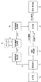
図1は本発明の第1実施形態における撮像システムのブロック図である。図1に示すように撮像システムは、光学系10a、撮像素子10、信号処理部21、時刻情報生成部22、カウンタ23、出力部25、同期信号出力部30、時刻情報取得部40、保存・表示部50を備える。
BEST MODE FOR CARRYING OUT THE INVENTION Hereinafter, embodiments of the present invention will be described in detail with reference to the drawings.
(First embodiment)
FIG. 1 is a block diagram of an imaging system according to the first embodiment of the present invention. As shown in FIG. 1, the imaging system includes an
撮像素子10は、本実施形態ではCMOSエリアセンサであり、2次元配列された複数の画素を有し、レンズなどの光学系10aを介して入射された光信号を電気信号である画素信号に変換する。
The
信号処理部21は、AFE(Analog Front End)、DSP(Digital Signal Processor)、フレームメモリなどから構成され、撮像素子10から出力された画素信号に対して信号処理を行う。AFEは、差動増幅器、クランプ回路、アナログ・デジタル変換回路を含み、アナログ・デジタル変換処理によってアナログの画素信号をデジタルの画素データに変換する。DSPは、ゲートアレイ回路などから構成され、オプティカル・ブラック画素を用いた処理、ガンマ処理などの階調補正、ホワイトバランス補正、デモザイク処理、ノイズ低減処理などを行う。フレームメモリは、画素データを一時的に保持するフレームメモリである。
The
同期信号出力部30は、クロック回路、カウンタ回路などを含み、撮像素子10の垂直同期信号VD、水平同期信号HDおよび撮像素子10の制御信号を生成する。同期信号出力部30は、撮像システム内部において設けられることを要せず、撮像システム外部から垂直同期信号VD、水平同期信号HDが供給されても良い。
The synchronizing
時刻情報取得部40は、複数のGPS(Global Positioning System)衛星からの電波を受信するアンテナ、ベースバンド信号を処理する受信回路、受信信号に含まれる情報を復調する復調回路を有している。複数のGPS衛星からの受信電波の時間差に基づき、撮像システムの緯度、経度、高度の正確な情報を取得することができる。また、GPS衛星からの受信電波には、基準時刻としてのGPS時刻情報(GPS週情報、GPS秒情報)、閏秒情報が含まれる。GPS週情報は1980年1月6日を起点として0~1023で巡回する情報である。GPS秒情報はGPS週内の秒経過情報であり、7日×24時間×60分×60秒=604800秒内の値を取り得る。閏秒情報はGPS時刻と世界標準時刻UTC(Universal Time Coordinated)との差分を表し、GPS時刻をUTCに変換する際に使用される。また、時刻情報取得部40は受信電波を復調する際にPPS(Pulse Per Second)信号と呼ばれる高精度の1秒1パルスの信号を出力する。
The time
時刻情報生成部22は、時刻情報取得部40から出力されたPPS信号、同期信号出力部30から出力された垂直同期信号VDを用いて、GPS時刻情報よりも時間分解能の高い時刻情報を生成する。時刻情報生成部22は例えば10MHz、すなわち10-7秒でカウントアップするカウンタ23を用いて計時し、PPS信号の立ち上がりでカウンタ23をリセットする。なお、PPS信号、垂直同期信号VDに加えて、水平同期信号HDを用いて、カウンタ23をリセットしても良い。PPS信号、水平同期信号HD、垂直同期信号VDをカウンタ23のリセットに用いることで、誤差が累積しない高精度の時刻情報を生成することができる。
The time
出力部25は、時刻情報生成部22によって生成された時刻情報を画像データに付加する。さらに、出力部25は時刻情報に加えて位置情報、撮像情報を画像データに付加することができる。保存・表示部50はフレーム毎の画像データを出力可能であって、デジタルインターフェース、メモリカードなどの記録媒体、ディスプレイなどの表示装置を含み得る。また、保存・表示部50は構内通信回線、公衆通信回線、インターネットなどに接続されても良い。
The
図2は撮像素子10のブロック図である。撮像素子10は、画素部100、行走査回路(行走査部)120、列読出回路(読出部)130A、130B、列走査回路150A、150B、制御部160、出力回路171A、172A、171B、172Bを備える。画素部100には、複数の画素110が行方向および列方向に沿って二次元マトリクス状に配置される。図2の画素部100はn行m列の画素110を含むが、説明の簡略化のために限られた数の画素110が示されている。なお、本明細書において、行方向とは図面における水平方向を示し、列方向とは図面において垂直方向を示すものとする。画素部100には、焦点検出用の信号を出力する焦点検出画素が配された測距行と、画像を生成するための信号を出力する撮像画素が配された複数の撮像行とが設けられている。また、画素部100の一部の画素110はOB画素(オプティカル・ブラック画素)として遮光されている。
FIG. 2 is a block diagram of the
画素110はカラーフィルタ、マイクロレンズ、光電変換部、浮遊拡散部、リセットトランジスタ、転送トランジスタ、増幅トランジスタ、選択トランジスタなどを含む。カラーフィルタは例えば赤、青、緑の原色フィルタであって、ベイヤー配列に従って各画素110に設けられている。
行走査回路120は制御部160からの制御信号を受けて、画素部100を行単位で読取走査を行う。すなわち、複数の画素110が配された画素行には行走査回路120から制御信号V1~Vnが供給され、光電変換された信号が画素110から読み出される。制御信号V1~Vnのそれぞれは、画素110に含まれるリセットトランジスタ、転送トランジスタ、選択トランジスタをオンまたはオフさせる制御信号を含む。列方向の複数の画素110は4×m本の列信号線L(1-1)~L(1-4)、・・・、L(m-1)~L(m-4)のそれぞれに接続されている。例えば、第1列の複数の画素110は列信号線L(1-1)、L(1-2)、L(1-3)、L(1-4)に接続され、第2列の複数の画素110は列信号線L(2-1)、L(2-2)、L(2-3)、L(2-4)に接続されている。列信号線L(1-1)、L(1-2)、・・・、L(m-1)、L(m-2)は列読出回路130Aの列回路131A、132Aにそれぞれ接続されている。
The
列回路131A、列回路132Aは列走査回路150Aによって走査され、出力回路171A、172Aに画素信号を順次出力する。同様に、列信号線L(1-3)、L(1-4)、・・・、L(m-3)、L(m-4)は列読出回路130Bの列回路131B、132Bにそれぞれ接続されている。列回路131B、列回路132Bは列走査回路150Bによって走査され、出力回路171B、172Bに画素信号を順次出力する。出力回路171A、172A、171B、172Bからの画素信号は図1の信号処理部21に出力される。
The
本実施形態においては、各列の画素110に4個の列回路131A、132A、131B、132Bが設けられているため、最大で4行の画素110からの画素信号を同時に読み出すことができる。なお、同時に読み出し可能な画素行は4行に限定されるものではなく、1行、2行でも良く、4行よりも多くても良い。さらに、複数行の画素信号を加算して読み出しても良い。
In this embodiment, four
列回路131A、132A、131B、132Bは増幅トランジスタの負荷となる定電流源115、画素信号を増幅する差動増幅回路、画素信号を一時的に保持する保持回路等を備える。制御部160は、垂直同期信号VD、水平同期信号HD、および図示されていない基準クロックに基づく制御信号を行走査回路120、列走査回路150A、150Bに出力する。
The
本実施形態の撮像素子10はプログレッシブスキャンにより4行×4列の16ch(チャンネル)の画素信号を同時に出力可能である。例えば、1フレームにおける走査行(走査回数)が300である場合、画素行の総数は4画素行×300=1200画素行となる。1水平走査あたりの列走査回数が540である場合、画素列の総数は4画素列×540=2160画素列となる。また、撮像素子10はローリングシャッタ動作可能であり、デジタル変換処理後の画像データは16ビットで出力されるものとする。なお、画素数、画像データのビット数は上述の例に限定されるものではない。
The
図3は、本実施形態に係る撮像素子10における画素110の等価回路を示している。画素110は、光電変換部PD、浮遊拡散部FD、転送トランジスタM1、増幅トランジスタM3、選択トランジスタM4、リセットトランジスタM5を備える。
FIG. 3 shows an equivalent circuit of the
光電変換部PDは、カラーフィルタ、マイクロレンズを通過した入射光を光電変換し、光電変換により生じた電荷を蓄積する。転送トランジスタM1は、オンとなることにより光電変換部PDの電荷を増幅トランジスタM3の浮遊拡散部FDに転送する。増幅トランジスタM3のドレインは電源電圧線に接続され、ソースは浮遊拡散部FDの電圧に基づく信号を選択トランジスタM4を介して列信号線Lに出力する。列信号線Lには定電流源115が接続されている。リセットトランジスタM5は、オンとなることにより浮遊拡散部FDの電圧をリセットする。
The photoelectric conversion unit PD photoelectrically converts incident light that has passed through the color filter and the microlens, and accumulates charges generated by the photoelectric conversion. When the transfer transistor M1 is turned on, it transfers the charge of the photoelectric conversion portion PD to the floating diffusion portion FD of the amplification transistor M3. The drain of the amplification transistor M3 is connected to the power supply voltage line, and the source outputs a signal based on the voltage of the floating diffusion portion FD to the column signal line L via the selection transistor M4. A constant
同一行の画素110に対しては共通の制御信号が行走査回路120から供給される。すなわち、同一行において、転送トランジスタM1、選択トランジスタM4、リセットトランジスタM5には、制御信号TX、SEL、RESがそれぞれ供給される。これらのトランジスタは、制御信号がハイレベルのときにオンとなり、ローレベルのときにオフとなる。なお、複数の画素110が1つの増幅トランジスタM3を共有しても良い。
A common control signal is supplied from the
図4は、本実施形態に係る制御信号のタイミングチャートであって、画素信号の読み出しの動作を表している。図4には、選択トランジスタM4に供給される制御信号SEL、リセットトランジスタM5に供給される制御信号RES、転送トランジスタM1に供給される制御信号TXが示されている。トランジスタM1、M4、M5はそれぞれ対応する制御信号がハイレベルの時にオンになり、ローレベルの時にオフになる。 FIG. 4 is a timing chart of control signals according to the present embodiment, showing the operation of reading out pixel signals. FIG. 4 shows the control signal SEL supplied to the select transistor M4, the control signal RES supplied to the reset transistor M5, and the control signal TX supplied to the transfer transistor M1. The transistors M1, M4 and M5 are turned on when the corresponding control signals are at high level and turned off when at low level.
以下、図2および図3を参照しながら、画素信号の読み出しの動作を説明する。まず、行走査回路120は制御信号SELをハイレベルとすることで、選択トランジスタM4をオンとし、信号を読み出す画素110を選択する。次に、行走査回路120は制御信号RESをハイレベルとし、リセットトランジスタM5をオンにする。リセットトランジスタM5がオンとなることで、浮遊拡散部FDの電圧が電源電圧にリセットされる。リセットトランジスタM5がオフとなった後、列読出回路130A、130Bは列信号線Lから、リセット時の画素信号の読み出し(N読み)を行う。行走査回路120は制御信号TXをハイレベルとすることで、転送トランジスタM1をオンとし、光電変換部PDの電荷を浮遊拡散部FDへ転送する。列読出回路130A、130Bは列信号線Lから光電変換時の画素信号の読み出し(S読み)を行う。このようにして読み出された画素信号は列読出回路130A、130Bにおいて相関二重サンプリング処理され、出力回路171A、172A、171B、172Bから出力される。なお、画素信号をAD変換した後に相関二重サンプリング処理を行っても良い。
Hereinafter, the operation of reading out pixel signals will be described with reference to FIGS. 2 and 3. FIG. First, the
図5は本実施形態における撮像システムの詳細なブロック図である。図5においては、図1に示された撮像システムのうちの主要な部分が、FPGA(Field Programmable Gate Array)20によって構成されている。以下、FPGA20の構成を中心に説明する。FPGA20は、信号処理部21、時刻情報生成部22、カウンタ23、出力部25、計算処理部241、ASCII変換部242、ヘッダ生成部243、画素カウンタ245、ブランクデータ付加部247を含む。
FIG. 5 is a detailed block diagram of the imaging system in this embodiment. In FIG. 5, the main part of the imaging system shown in FIG. 1 is configured by an FPGA (Field Programmable Gate Array) 20. The configuration of the
信号処理部21は、DSP(Digital Signal Processor)、フレームメモリなどから構成される。信号処理部21は、撮像素子10から出力された画素信号に対してアナログ・デジタル変換処理、オプティカル・ブラック画素を用いた処理、ガンマ処理などの階調補正、ホワイトバランス補正、デモザイク処理、ノイズ低減処理などを行う。フレームメモリは、画素データを一時的に保持するフレームメモリである。
The
時刻情報生成部22は図1において説明したように、PPS信号、垂直同期信号VDを用いてカウンタ23をリセットし、GPS時刻情報よりも時間分解能の高い時刻情報t(h)を生成する。
As described with reference to FIG. 1, the
計算処理部241は、時刻情報t(h)を用いて、フレームの露光開始時刻、露光終了時刻、露光時間を算出する。ASCII変換部242は、FITS(Flexible Image Transport System)フォーマットに基づき、露光開始時刻、露光終了時刻、露光時間に加えて、GPS情報、撮像情報、固定値などの情報をASCII(American Standard Code for Information Interchange)形式のデータに変換する。FITSフォーマットは、たとえば宇宙天文分野などにおいて利用される汎用フォーマットである。GPS情報は、位置情報(緯度情報、経度情報)、GPS時刻を世界標準時刻(UTC)に変換する際に使用される閏秒情報、GPS時刻情報(GPS週情報、GPS秒情報)などを含む。また、GPS情報は、PPS信号を基準としたμ秒刻みの時間情報を含み得る。
The calculation processing unit 241 calculates the exposure start time, the exposure end time, and the exposure time of the frame using the time information t(h). The
撮像情報は、撮像条件などを表す情報であって、撮像システムの情報、撮像素子10の情報、光学系10aの情報を含み、画像データの処理に用いられ得る。撮像システムの情報は、撮像システムの名称、シリアル番号などを含み、撮像素子10の情報は、露光時間、フレーム番号、ゲイン設定値、温度、シリアル番号などを含み得る。光学系10aの情報は、レンズの種類、F値、ズーム位置などを含む。固定値は、後述するFITSフォーマットにおけるコメント、キーワードなどの情報を含み得る。ヘッダ生成部243は、ASCII変換部242によって変換されたASCII形式のデータをFITSフォーマットに従い並べ替え、FITSヘッダを生成する。生成されたFITSヘッダは出力部25に入力される。
The imaging information is information representing imaging conditions and the like, and includes information on the imaging system, information on the
画素カウンタ245は信号処理部21から順に出力される画像データを画素毎にカウントする。ブランクデータ付加部247は、画素カウンタ245によってカウントされた画素数が予め定められたFITSブロック数に満たない場合、ブランクデータを出力する。出力部25には、ヘッダ生成部243からのFITSヘッダ、信号処理部21からの画像データ、ブランクデータ付加部247からのブランクデータが入力される。出力部25は、FITSヘッダ、画像データ、ブランクデータをFITSフォーマットに従ったタイミングで切り替える。出力部25は、FITSヘッダの最後を表すキーワード(「END」)をFITSヘッダにおいて検出すると、出力部25は、出力信号をFITSヘッダから画像データに切り替える。これにより、画像データがFITSヘッダに続いて出力される。
The
図6は、本実施形態における撮像システムのタイミングチャートであって、垂直同期信号VD、水平同期信号HD、カウンタ、PPS信号、画素出力、出力信号を表している。カウンタは時刻情報生成部22において10-7秒毎にカウントアップされ、GPSのPPS信号の立ち上がりでリセットされるデジタル値である。
FIG. 6 is a timing chart of the imaging system in this embodiment, showing the vertical synchronization signal VD, horizontal synchronization signal HD, counter, PPS signal, pixel output, and output signal. The counter is a digital value that is counted up every 10 −7 seconds in the
撮像システムに電源が投入されることにより、同期信号出力部30は垂直同期信号VD、水平同期信号HD、制御信号を出力し、撮像素子10は撮像動作を開始する。時刻情報取得部40はGPS衛星から電波を受信し、GPS位置情報、GPS時刻情報を取得し始める。
When the imaging system is powered on, the synchronizing
時刻t1において、時刻情報取得部40は受信電波からPPS信号を取得すると、PPS信号を時刻情報生成部22に出力する。時刻情報生成部22はPPS信号の立ち上がりを検出すると、カウンタをリセットする。PPS信号に同期してリセットされるカウンタ23を用いることで、GPS時刻情報の更新周期である1秒よりも時間分解能の高いμ秒単位の時刻情報を生成することができる。時刻t1と同時に、時刻情報取得部40は受信電波からGPS週情報、GPS秒情報を含むGPS時刻情報を取得し、GPS時刻情報を年/月/日/時/分/秒の形式の時刻情報に変換する。GPS時刻情報は、撮像素子10の駆動タイミングとは非同期に、PPS信号の1秒毎に取得される。
At time t<b>1 , the time
時刻t2において、垂直同期信号VDがハイレベルになった後、ローレベルになると、撮像素子10において1フレームの垂直走査期間が始まる。垂直同期信号VDはPPS信号とは非同期の信号である。時刻情報生成部22は時刻t2におけるカウンタの値を時刻情報t2(h)として出力部25に出力する。期間T1において、出力部25は時刻情報t2(h)および位置情報等をFITSヘッダとして出力する。これにより、第1の垂直走査期間の開始の時刻t2を10-7秒の時間分解能で記録することができる。期間T1は信号処理期間に対応し、期間T1において信号処理部21は、アナログ・デジタル変換処理、ガンマ処理などの階調補正処理、ホワイトバランス補正処理、デモザイク処理、ノイズ低減処理、OBを利用した信号処理などを行う。期間T1における信号処理は、必ずしもこれらの例に限定されず、画像データの遅延期間、ブランキング期間、画像データが出力されるまでの期間、信号出力の遅延時間であってもよい。すなわち、期間T1は、画像データの信号処理、出力などに要する様々な期間を含み得る。
At time t2, when the vertical synchronizing signal VD changes to high level and then to low level, the
時刻t3において、水平同期信号HDがハイレベルになった後、ローレベルになると、撮像素子10において第1の水平走査期間が始まる。なお、以下の説明において、水平同期信号HDの立ち上がりおよび立ち下がり時刻を併せて水平走査期間の開始時刻と称することがある。撮像素子10において、行走査回路120は第1~第4の画素行を選択し、列読出回路130A、130Bは4行分の画素信号を読み出す。信号処理部21は画素信号をデジタルの画像データに変換し、画像データに対してノイズリダクション、ゲイン処理などの信号処理を行う。以下、同様にして、水平走査期間毎に4行分の画素信号が読み出され、信号処理部21においてデジタル信号の画像データに変換される。期間T1の経過後において、出力部25は、第1の垂直走査期間における画像データを出力する。
At time t3, when the horizontal synchronizing signal HD becomes low level after becoming high level, the first horizontal scanning period starts in the
時刻t2-2において、垂直同期信号VDがハイレベルになった後、ローレベルになると、第2のフレームの垂直走査期間が始まる。時刻情報生成部22は時刻t2-2におけるカウンタの値を時刻情報t2(h)-2として出力部25に出力する。期間T1-2において、出力部25はFITSヘッダを出力する。すなわち、画像データが信号処理部21から出力される前に、第2のフレームに関連付けられた時刻情報t2(h)-2が出力される。期間T1-2の経過後において、出力部25は第2のフレームの画像データを出力する。このようにして、画像データが信号処理部21から出力される前に、高精度の時刻情報が、垂直走査期間毎、すなわちフレーム毎に生成および出力される。
At time t2-2, when the vertical synchronizing signal VD becomes high level and then becomes low level, the vertical scanning period of the second frame starts. The time
図7は本実施形態における時刻情報の画像データへの付加方法を説明するための図であって、出力部25から出力された1フレームの画像データおよびヘッダを表している。1フレームの画像データは、データ部A1、A2、A3を含む。データ部A1は水平OB画素領域に対応し、データ部A2は垂直OB画素領域に対応している。データ部A3は有効画素領域に対応している。
FIG. 7 is a diagram for explaining a method of adding time information to image data in this embodiment, and shows one frame of image data output from the
データ部A0は時刻情報などのFITSヘッダに対応し、1フレームの画像データの上部(先の時刻)に付加される。1画素のデータが16bitのデータ、すなわち2バイトで表される場合、1画素にアスキーコード、その他2バイト文字などの情報をデータ部A0に書き込むことができる。 The data part A0 corresponds to the FITS header such as time information, and is added to the upper part (previous time) of the image data of one frame. When the data of one pixel is represented by 16-bit data, that is, two bytes, information such as an ASCII code and other two-byte characters can be written to the data section A0 in one pixel.
なお、水平OB画素のデータ部A1あるいは垂直OB画素のデータ部A2を時刻情報に置き換え、水平走査期間毎に高精度の時刻情報を付加しても良い。この場合、時刻情報を確定するタイミングは、水平同期信号HDすなわち一走査行の画像データの出力開始時である。このため、水平同期信号HDにもっとも近い水平OBの先頭部分のデータを時刻情報のデータ部A1に置き換えても良い。 Note that the data portion A1 of the horizontal OB pixels or the data portion A2 of the vertical OB pixels may be replaced with time information, and highly accurate time information may be added for each horizontal scanning period. In this case, the timing for determining the time information is the horizontal synchronizing signal HD, that is, the start of output of image data for one scanning line. Therefore, the data at the beginning of the horizontal OB closest to the horizontal synchronizing signal HD may be replaced with the data portion A1 of the time information.
続いて、本実施形態における出力信号の詳細を図8、図9、図10を参照しながら説明する。図8は本実施形態における出力信号の詳細を表す図である。図9、図10はFITSフォーマットを説明するための図である。 Next, the details of the output signal in this embodiment will be described with reference to FIGS. 8, 9 and 10. FIG. FIG. 8 is a diagram showing the details of the output signal in this embodiment. 9 and 10 are diagrams for explaining the FITS format.
FITSフォーマットのファイルは、ASCIIテキストで表されたメタデータであるFITSヘッダB0と、ASCIIもしくはバイナリのデータ配列B1とから構成される。本実施形態において、出力部25からの出力信号は、FITSヘッダB0とバイナリのデータ配列B1とを含む。すなわち、図8に示されるように、出力部25は、期間T1、T1-2において時刻情報などのFITSヘッダB0を出力し、期間T1、T1-2経過後にバイナリのデータ配列B1を出力する。FITSヘッダB0およびデータ配列B1は複数のFITSブロック(レコード)から構成され、1つのFITSブロックのサイズは2880バイト(23040bit)である。本実施形態の撮像システムによって得られる画像データは水平画素数2160、垂直画素数1200、1画素のデータは16bitであるので、1フレームの画像データは2160×1200×16=441472000bitのデータから構成される。このため、1フレームの画像データを1800個(441472000÷23040=1800)のFITSブロックで構成することができる。ここで、出力部25は、時刻情報および撮像情報などを、画像データにおける1画素のビット数と同じビット数のデータに変換し、画像データにFITSヘッダを付加することにより、画像データをFITSデータとして取り扱うことができる。
A FITS format file consists of a FITS header B0, which is metadata expressed in ASCII text, and an ASCII or binary data array B1. In this embodiment, the output signal from the
図9に示されるように、1つのFITSブロックは複数のキーワードレコードを含み、それぞれのキーワードレコードは80バイト(80文字)の情報から構成される。このようにして構成されたFITSヘッダB0は、データの目的、種類、構造、バイト数、レコード数等のデータに関する情報を表し得る。1つのFITSブロックには、2880バイト/80バイト=36行の文字列を記述することができる。FITSヘッダが36行を超える場合は、複数のFITSブロックを用いることが可能である。また、FITSヘッダB0が1個のFITSブロックに満たない場合には、FITSブロックの残りの領域はブランクデータで埋められる。 As shown in FIG. 9, one FITS block includes a plurality of keyword records, and each keyword record consists of 80 bytes (80 characters) of information. The FITS header B0 constructed in this manner can represent information about the data such as the purpose, type, structure, number of bytes, number of records, etc. of the data. Character strings of 2880 bytes/80 bytes=36 lines can be described in one FITS block. If the FITS header exceeds 36 lines, multiple FITS blocks can be used. Also, if the FITS header B0 is less than one FITS block, the remaining area of the FITS block is filled with blank data.
データ配列B1は、FITSヘッダB0と同様に、1つ以上のFITSブロックから構成される。1フレームの画像データが2880バイトを超える場合、データ配列B1には複数のFITSブロックが含まれ得る。また、1フレームの画像データが1個のFITSブロックに満たない場合には、出力部25はFITSブロックの残りの領域をブランクデータで埋める。データ配列B1には、1行毎の画像データが順に配列される。すなわち、1フレームの画像データの垂直OB画素の読み出し期間においては、データ部A1、A2が出力部25から交互に出力され、有効画素領域の読み出し期間においては、データ部A1、A3が出力部25から交互に出力される。
Data array B1 is composed of one or more FITS blocks, similar to FITS header B0. If the image data for one frame exceeds 2880 bytes, the data array B1 may contain multiple FITS blocks. Also, when the image data of one frame is less than one FITS block, the
FITSヘッダB0の一例を図10に示す。FITSヘッダB0は、それぞれが80文字(80桁)の複数のキーワードレコードから構成され、キーワードレコードの数は無制限である。但し、必要なキーワードおよびキーワードの順序は定められており、最後のキーワードレコードは「END」というキーワードで示される。キーワードレコードは、「キーワード=値/コメント」で表され、第1~第8桁のキーワード(8文字以下の左詰めされたASCIIコード)、第9桁の「=」(等号)、第10桁の「 」(16進のASCIIコードの「0x20」または「20H」で表されるブランク)を含む。但し、「HISTORY」、「COMMENT」、空白のキーワードは例外で、上述の規則に従わない。また、キーワードは大文字で表され、コメントは小文字で表される。 An example of the FITS header B0 is shown in FIG. The FITS header B0 consists of a plurality of keyword records of 80 characters (80 digits) each, and the number of keyword records is unlimited. However, the necessary keywords and the order of the keywords are defined, and the last keyword record is indicated by the keyword "END". A keyword record is expressed as "keyword=value/comment", with the first to eighth keywords (8 characters or less left-aligned ASCII code), the ninth "=" (equal sign), the tenth Contains the digit " " (a blank represented by the hexadecimal ASCII code "0x20" or "20H"). The exceptions are "HISTORY", "COMMENT" and blank keywords, which do not follow the above rules. Also, keywords are shown in uppercase letters and comments are shown in lowercase letters.
値(パラメータ)は、一定のフォーマットに従って記述される。いくつかの必須パラメータは一定のフォーマットで記述されることが要求され、その他のパラメータについてもフォーマットに従って記述されることが推奨されている。文字型の変数の標準文字数は8文字であるが、必ずしも8文字に限定されない。文字型の変数の第11桁には「’」が記述され、続けて文字列および終端の「’」が記述される。論理型の変数の第30桁には「T」または「F」が記述される。整数型の変数の第11~30桁には右揃えで変数が記述される。また、実数型の変数の第11~30桁には右揃えで変数が記述される。実数型の変数に小数部がある場合には小数点が記述され、変数に指数部がある場合には「E」または「D」が記述される。最小限必要なキーワードは、「SIMPLE」、「BITPIX」、「NAXIS」、「NAXISn」、「END」であって、「SIMPLE」から「NAXISn」までの記述の順序は上述のフォーマットに従い定められている。 Values (parameters) are written according to a certain format. Some mandatory parameters are required to be described in a certain format, and other parameters are also recommended to be described according to the format. The standard number of characters for a character type variable is 8 characters, but it is not necessarily limited to 8 characters. In the eleventh digit of the character type variable, "'" is described, followed by a character string and a terminating "'". ``T'' or ``F'' is written in the 30th digit of a Boolean variable. Variables are written right justified in the 11th to 30th digits of integer type variables. In addition, the variables are written right justified in the 11th to 30th digits of the real number type variables. If the real number type variable has a decimal part, a decimal point is described, and if the variable has an exponent part, "E" or "D" is described. The minimum required keywords are "SIMPLE", "BITPIX", "NAXIS", "NAXISn", and "END", and the order of descriptions from "SIMPLE" to "NAXISn" is defined according to the above format. there is
「SIMPLE」は論理型の変数であって、ファイルがFITS規格に適合するかどうかを示す。「BITPIX」は整数型の変数であって、各データの値を何ビットで表現しているかを示す。「NAXIS」は整数型の変数であって、データ配列の座標軸の本数を示す。「NAXISn」は整数型の変数であって、「n」は1から「NAXIS」の値までを示し、それぞれ第n軸に沿ったデータの数を示す。「END」は値を持たず、第9~80桁は空白で埋められ、ヘッダレコードの終了を表す。本実施形態において、出力部25がFITSヘッダB0において「END」を検出すると、出力信号をFITSヘッダB0からデータ配列B1に切り替える。「/」(スラッシュ)は、パラメータの後の任意の場所に記述され、スラッシュの後ろには少なくとも1つの空白に続いてコメントが記述される。本実施形態においては、スラッシュの後ろにキーワードのコメントが記述されているが、その他の情報が記述されても良い。また、スラッシュの後ろは空白であっても良い。
"SIMPLE" is a boolean variable that indicates whether the file conforms to the FITS standard. "BITPIX" is an integer type variable and indicates how many bits each data value is expressed. "NAXIS" is an integer type variable that indicates the number of coordinate axes in the data array. "NAXISn" is an integer type variable, where "n" indicates a value from 1 to "NAXIS", each indicating the number of data along the nth axis. "END" has no value and digits 9-80 are filled with blanks to indicate the end of the header record. In this embodiment, when the
図10において、「SIMPLE」~「BSCALE」は、前述の通り固定の情報である。「BITPIX」~「BSCALE」は、本実施形態の撮像システムにおいて取得する画像データの仕様を表している。例えば、各画素値は16bitで表されるため、「BITPIX」の値は「16」となる。また、画像データは2次元の画像データなので「NAXSIS」の値は「2」となる。「NAXIS1」は画像の水平画素数を表し、例えば「2160」であり、「NASIS2」は画像の垂直画素数を表し、例えば「1200」である。「SIMPLE」、「EXTEND」、「COMMENT」は、FITSフォーマットに対する情報である。「BZERO」は、画素値を物理値に変換するゼロ点を表し、「BSCALE」は、画像値を物理値に変換するスケールを表す。 In FIG. 10, "SIMPLE" to "BSCALE" are fixed information as described above. "BITPIX" to "BSCALE" represent specifications of image data acquired by the imaging system of this embodiment. For example, since each pixel value is represented by 16 bits, the value of "BITPIX" is "16". Also, since the image data is two-dimensional image data, the value of "NAXSIS" is "2". "NAXIS1" represents the number of horizontal pixels of the image, for example "2160", and "NASIS2" represents the number of vertical pixels of the image, for example "1200". "SIMPLE", "EXTEND", and "COMMENT" are information for the FITS format. "BZERO" represents a zero point for converting pixel values into physical values, and "BSCALE" represents a scale for converting image values into physical values.
「EXPTIME」~「DATE」は、フレームの撮影に対応した時刻情報である。「EXPTIME」は、フレームあたりの露光時間を表し、撮像システムの設定値から取得される。「S-OPEN」は、フレームの露光開始時刻であり、本実施形態におけるフレームの撮影開始の垂直同期信号VDの立ち上がり時刻から生成された高精度な時刻情報t(h)である。「S-CLOSE」は、フレームの露光終了時刻であり、「EXPTIME」と「S-OPEN」から算出される。時刻情報t(h)は、絶対時刻情報であるGPSのPPS信号に基づいて生成される。PPS信号の取得が有効である場合、「GPS-STAT」には「LOCKED」が記述され、PPS信号の取得が無効である場合、「GPS-STAT」には「UNLOCKED」が記述される。このように、「GPS-STAT」を参照することにより、「S-OPEN」および「S-CLOSE」の正誤を判定することが可能となる。 "EXPTIME" to "DATE" are time information corresponding to frame shooting. "EXPTIME" represents the exposure time per frame and is obtained from the settings of the imaging system. “S-OPEN” is the frame exposure start time, which is highly accurate time information t(h) generated from the rise time of the vertical synchronization signal VD at the start of frame shooting in this embodiment. "S-CLOSE" is the frame exposure end time, which is calculated from "EXPTIME" and "S-OPEN". The time information t(h) is generated based on the PPS signal of GPS, which is absolute time information. If the acquisition of the PPS signal is valid, "LOCKED" is described in "GPS-STAT", and if the acquisition of the PPS signal is invalid, "UNLOCKED" is described in "GPS-STAT". Thus, by referring to "GPS-STAT", it is possible to judge whether "S-OPEN" and "S-CLOSE" are correct or not.
「DATE」は、撮像システムのシステム時刻から取得されたフレームの撮影開始時刻である。システム時刻は例えば、撮像システム内部に設けられたクロック回路から供給され得る。「DATE」は、撮像システムのシステム時刻であるため、時刻情報t(h)のように必ずしも高精度の時刻情報ではない。しかしながら、GPSの時刻情報が取得されなかった場合に、「DATE」は代替的に用いられ得る。「FRAME-NO」は、フレーム番号を表し、フレーム毎にカウントアップされる。「FRAME-NO」を参照することにより、連続撮影されたフレームの欠落を確認することが可能となる。「CAM-GAIN」は撮像素子10のゲイン設定値を表し、「LENS-F」は光学系10aにおけるレンズのF値を表す。
“DATE” is the shooting start time of the frame obtained from the system time of the imaging system. The system time can be supplied, for example, from a clock circuit provided within the imaging system. Since "DATE" is the system time of the imaging system, it is not necessarily highly accurate time information like the time information t(h). However, "DATE" may be used alternatively if GPS time information was not obtained. "FRAME-NO" represents a frame number, which is counted up for each frame. By referring to "FRAME-NO", it is possible to confirm the omission of consecutively shot frames. "CAM-GAIN" represents the gain setting value of the
上述した値のうち、「S-OPEN」(時刻情報t(h))、「EXPTIME」、「S-CLOSE」のそれぞれの値はヘッダ生成部243においてリアルタイムに生成される。また、「SIMPLE」、「BITPIX」、「NAXIS」、「NAXIS1」、「NAXIS2」、「EXTEND」、「COMMENT」、「BZERO」、「BSCALE」、「/」(スラッシュ)以降のコメントなどは固定値としてFITSヘッダに含められる。すなわち、これらの固定値は、時刻情報、撮像システムの設定値等、リアルタイムで生成される情報と合わせて、指定されたキーワードレコードの順に合成され、FITSヘッダとして出力される。 Among the values described above, the values of “S-OPEN” (time information t(h)), “EXPTIME”, and “S-CLOSE” are generated in real time by the header generator 243 . In addition, "SIMPLE", "BITPIX", "NAXIS", "NAXIS1", "NAXIS2", "EXTEND", "COMMENT", "BZERO", "BSCALE", comments after "/" (slash) are fixed. Included in the FITS header as a value. That is, these fixed values are combined with information generated in real time, such as time information and setting values of the imaging system, and synthesized in the order of designated keyword records, and output as a FITS header.
各キーワード、固定値、コメントは、撮像システムおよび撮像素子に関する情報であって、フレームの取り込みのタイミングに関係なく取得または生成可能である。このため、垂直同期信号VDの立ち上がりの前に固定値等を予め取得または生成し、ASCII文字に変換して撮像システム内に保持することができる。また、撮像システムおよび撮像素子から情報を取得せずに、予め定められた値をASCII文字の固定値として保持しておいてもよい。 Each keyword, fixed value, and comment are information about the imaging system and the imaging device, and can be obtained or generated regardless of the frame capture timing. Therefore, a fixed value or the like can be obtained or generated in advance before the rise of the vertical synchronization signal VD, converted into ASCII characters, and stored in the imaging system. Alternatively, a predetermined value may be held as a fixed value of ASCII characters without obtaining information from the imaging system and the imaging device.
なお、本実施形態において、固定値は「SIMPLE」~「BSCALE」であるが、撮像素子、画像データに応じて他の情報を固定値としても良い。例えば、「CAM-GAIN」、「LENS-F」などのようにフレーム毎に変化しない値を固定値として予め保持もよい。撮像時に取得される情報を予め定められた固定値としても良い。さらに、撮像システムの名称、撮像素子および撮像システムのシリアル番号、撮像素子および撮像システムの温度情報、GPSの時刻情報、経度緯度情報、レンズの種類、ズーム位置情報等を固定値としても良い。固定値の情報、各キーワードにおいて上述されていないルールは、FITSの規格に従う。 In this embodiment, the fixed values are "SIMPLE" to "BSCALE", but other information may be fixed values depending on the image sensor and image data. For example, values that do not change for each frame, such as "CAM-GAIN" and "LENS-F", may be stored in advance as fixed values. Information acquired at the time of imaging may be a predetermined fixed value. Furthermore, the name of the imaging system, serial number of the imaging device and imaging system, temperature information of the imaging device and imaging system, GPS time information, longitude/latitude information, lens type, zoom position information, etc. may be fixed values. Fixed value information and rules not described above for each keyword comply with the FITS standard.
以上述べたように、本実施形態においては、画像データがフレーム単位で信号処理部21から出力される前に時刻情報を生成および出力することにより、フレームの欠落を回避し、時刻情報および画像データを安定して出力することが可能となる。ここで、比較例として、画像データが出力部25から出力されるまで時刻情報を保持し、1フレームの画像データを出力する段階において、時刻情報を画像データに付加する場合を検討する。この場合、メモリに保持された時刻情報の読み出し、画像データのFITSデータ形式への変換、時刻情報と他の情報とを合わせたFITSヘッダの生成、FITSヘッダの画像データへの付加などの一連の処理を同時に実行する必要がある。高速度連続撮影時においては、連続したすべてのフレームにおける処理が間に合わず、フレームの欠落が発生し、画像の記録精度が損ねられてしまう。特に、宇宙天文分野において地球に近い軌道の観測では60fps以上が要求され、近年の科学計測用のカメラにおいては100fps以上が要求されており、フレームの欠落が発生し得る。これに対して、本実施形態によれば、画像データが信号処理部21から出力される前の信号処理期間において、FITSヘッダを生成および出力しているため、FITSヘッダの生成および出力によって画像データの出力期間は制限されない。すなわち、画像データの信号処理期間を利用してFITSヘッダを生成および出力することにより、高速度動画撮影時におけるフレームの欠落を回避し、高精度の時刻情報を有するFITSファイルを出力することが可能となる。
As described above, in the present embodiment, the time information is generated and output before the image data is output from the
天体観測において、流星、スペースデブリ等の移動体を動画撮影する場合、移動体の正確な軌道を算出するためには、移動体の位置情報およびその正確な絶対時刻情報が重要となる。ここで、絶対時刻はたとえばUTC(世界協定時)で規定される国際原子時などを示す。また、遠方の対象を観察する所謂リモートセンシングの分野では、移動体の撮影、もしくは航空機、人工衛星など移動体からの撮影が行われる。その際においても、地球に対する対象物の位置、正確な時刻情報があれば、対象物についてさらにより多くの情報を得ることができる。本実施形態によれば、例えば、天体観測において、流星、スペースデブリ等の移動体を動画撮影する場合に、フレームと正確な絶対時刻情報とを関連付けて記録することが可能となる。 In astronomical observation, when moving images of moving objects such as meteors and space debris are taken, position information of the moving objects and accurate absolute time information are important for calculating accurate orbits of the moving objects. Here, absolute time indicates, for example, international atomic time defined by UTC (Universal Coordinated Time). Further, in the field of so-called remote sensing, which observes distant objects, photographing of moving objects or photographing from moving objects such as airplanes and artificial satellites is performed. Even in that case, if the position of the object with respect to the earth and accurate time information are available, it is possible to obtain much more information about the object. According to this embodiment, for example, when moving images of moving objects such as meteors and space debris are captured in astronomical observation, it is possible to record frames in association with accurate absolute time information.
また、本実施形態において、高精度の時刻情報を確定するタイミングは、垂直同期信号VD、すなわち1フレーム画像データの取得開始時刻である。画像データよりも前に時刻情報を確定し、出力することで、時刻情報をFITSファイルのFITSヘッダとして扱うことができる。なお、本発明は必ずしもFITSファイルを用いることを要せず、撮影の時刻情報を付加することができれば、FITSファイル以外のフォーマットを用いても良い。例えば、図8において、垂直OB画素領域(データ部A2)の上側、すなわち先の時刻のデータ部A0の下位bitに時刻情報を埋め込み、出力してもよい。また、電子シャッタによる全画素一括露光の場合、水平OB画素領域(データ部A1)の左側、すなわち先の時刻に時刻情報を出力しても良い。水平OB画素領域(データ部A1)あるいは垂直OB画素領域(データ部A2)を時刻情報に置き換えて出力しても良い。さらに、水平OB画素領域(データ部A1)および垂直OB画素領域(データ部A2)を除いて、ヘッダ(データ部A0)と有効画素領域(データ部A3)のみを出力しても良い。また、FITSファイルとして出力する場合においても、ヘッダに続いて有効画素領域のみを出力しても良い。 Further, in the present embodiment, the timing for determining highly accurate time information is the acquisition start time of the vertical synchronization signal VD, that is, one frame image data. By determining and outputting the time information before the image data, the time information can be handled as the FITS header of the FITS file. It should be noted that the present invention does not necessarily require the use of a FITS file, and a format other than the FITS file may be used as long as it is possible to add time information of photographing. For example, in FIG. 8, the time information may be embedded in the upper side of the vertical OB pixel area (data portion A2), that is, in the lower bits of the data portion A0 of the previous time, and output. Further, in the case of all-pixel batch exposure by an electronic shutter, the time information may be output on the left side of the horizontal OB pixel area (data section A1), that is, at the previous time. The horizontal OB pixel area (data portion A1) or the vertical OB pixel area (data portion A2) may be replaced with time information and output. Furthermore, only the header (data section A0) and effective pixel area (data section A3) may be output, excluding the horizontal OB pixel area (data section A1) and the vertical OB pixel area (data section A2). Also, when outputting as a FITS file, only the effective pixel area may be output following the header.
出力部25は各フレームに時刻情報を付加しているが、本発明はこれに限定されない。例えば、時刻情報を格納するフレームは、偶数フレーム、奇数フレームのように2フレームのうちの1フレーム、あるいは任意の複数フレームのうちの1フレームであっても良く、ランダムに選択されたフレームであっても良い。さらに、被写体であると認識されたフレームにのみ時刻情報を格納しても良い。また、時刻情報と撮像されたフレームとの関連付けが明確である限り、画像データとは別に時刻情報を出力しても良い。このように、時刻情報を格納するフレームは、画像データの出力フォーマット、メモリ容量、撮像素子の駆動の仕様、取得した情報などの条件に応じて適宜変更可能である。
Although the
本実施形態では、10-7秒単位のカウンタの基準となる時刻情報を、GPS衛星から得られるPPS信号としたが、本発明はこれに限られるものではない。例えば、標準電波を受信しても良く、時刻サーバの情報をネットワークから取得しても良い。また、同期信号VD、HDは同期信号出力部30によって生成されているが、撮像素子10によって生成された同期信号を検出して、カウンタの取り込み時刻(図6の時刻t2)を取得しても良い。さらに、カウンタは、10MHz、すなわち10-7秒の周期であるが、カウンタの基準となるPPS信号、高い時間分解能を有する限り、上述の例に限定されない。また、本実施形態では、時刻情報生成部22が、撮像素子10の外部に設けられた例を説明したが、撮像素子10が時刻情報生成部22を有していてもよい。
In this embodiment, the PPS signal obtained from the GPS satellite is used as the time information that serves as the reference for the counter in units of 10 −7 seconds, but the present invention is not limited to this. For example, standard radio waves may be received, and information on a time server may be obtained from a network. In addition, although the synchronization signals VD and HD are generated by the synchronization
また、本実施形態において、時刻情報の取り込みのタイミングは垂直同期信号VDの立ち上がり時刻(図6の時刻t2)であるが、フレームと関連付けられている限り、様々な時刻を基準とすることができる。例えば、垂直同期信号VDの立ち下がり時刻において時刻情報を取り込んでもよく、垂直同期信号VDに同期した水平走査開始のタイミングにおいて時刻情報を取り込んでも良い。また、時刻t2から出力部25が画像データを出力する時刻までの時間を計測し、計測された時間を時刻t2に加算した値を時刻情報として出力しても良い。さらに、各フレームの露光開始時刻または終了時刻を用いても良い。上述したように、垂直同期信号VDに同期したタイミングである限り、様々なタイミングにおいて時刻情報を取り込むことが可能である。
Also, in the present embodiment, the timing for capturing the time information is the rising time of the vertical synchronization signal VD (time t2 in FIG. 6), but as long as it is associated with the frame, various times can be used as the reference. . For example, the time information may be fetched at the fall time of the vertical synchronizing signal VD, or the time information may be fetched at the horizontal scanning start timing synchronized with the vertical synchronizing signal VD. Alternatively, the time from the time t2 to the time when the
(第2実施形態)
続いて、第2実施形態における撮像システムを説明する。第1実施形態において撮像素子10はローリングシャッタにより動作するが、本実施形態における撮像素子10は一括電子シャッタにより動作することが可能である。以下、本実施形態について、第1実施形態と異なる構成を中心に説明する。
(Second embodiment)
Next, an imaging system according to the second embodiment will be described. In the first embodiment, the
図11は本発明の第2実施形態における撮像システムのブロック図である。撮像システムは、光学系10a、撮像素子10、信号処理部21、時刻情報生成部22、カウンタ23、出力部25、制御信号出力部31、時刻情報取得部40、保存・表示部50を備える。制御信号出力部31は光電変換部PDを一括してリセットするための制御信号OFGを撮像素子10および時刻情報生成部22に出力する。制御信号OFGがハイレベルからローレベルになることで、画素部100における一括露光が開始する。時刻情報生成部22は制御信号TX1がハイレベルからローレベルになった時刻におけるカウンタの値を高精度の時刻情報として出力することができる。
FIG. 11 is a block diagram of an imaging system according to the second embodiment of the present invention. The imaging system includes an
図12は、本実施形態に係る画素110の等価回路を示している。画素110は、光電変換部PD、保持部C1、浮遊拡散部FD、第1の転送トランジスタM1、第2の転送トランジスタM2、増幅トランジスタM3、選択トランジスタM4、リセットトランジスタM5、オーバーフロートランジスタM6を備える。第1の転送トランジスタM1は、オンとなることにより光電変換部PDの電荷を保持部C1に転送し、保持部C1は、光電変換部PDから転送された電荷を保持する。全画素110において、第1の転送トランジスタM1を同時に駆動することにより、光電変換部PDの露光終了のタイミングを一括して制御することが可能となる。すなわち、各行の制御信号TX1を同時にオンまたはオフに制御することにより、全画素110における露光タイミングを同時に制御することができる。オーバーフロートランジスタM6はオンとなることにより、光電変換部PDの電荷を電源ノードなどのオーバーフロードレインに排出することができる。本実施形態によれば、保持部C1が電荷を保持している間、光電変換部PDは新たに生じた電荷を蓄積することができ、全画素110における光電変換のタイミングを一致させる一括電子シャッタ機能を実現することができる。
FIG. 12 shows an equivalent circuit of the
図13は本実施形態における撮像システムのタイミングチャートである。時刻t1において、時刻情報生成部22は、PPS信号の立ち上がりを検出すると、カウンタをリセットし、10-7秒毎にカウンタをカウントアップする。全画素110において制御信号OFGがハイレベルとなることでオーバーフロートランジスタM6がオンとなり、光電変換部PDの電荷が排出される。時刻t4において、制御信号OFGがハイレベルからローレベルとなることで、オーバーフロートランジスタM6がオフとなり、全画素110において光電変換部PDにおける露光期間が開始する。同時に、時刻情報生成部22は時刻t4におけるカウンタの値を時刻情報t4(h)として出力部25に出力する。期間T1(時刻t4~時刻t5)において、出力部25は時刻情報t4(h)および位置情報等をFITSヘッダとして出力する。
FIG. 13 is a timing chart of the imaging system according to this embodiment. At time t1, when the
全画素110において制御信号TX1がハイレベルとなり、第1の転送トランジスタM1がオンとなることで、光電変換部PDの電荷が保持部C1に転送される。時刻t5において、全画素110において制御信号TX1がローレベルになり、露光期間が終了する。その後、それぞれの行の画素信号が列読出回路130A、130Bによって順序読み出され、撮像素子10から出力される。出力部25は1フレームの画像データの前に時刻情報を含むFITSヘッダを付加する。これにより、全画素110の露光開始の時刻情報t4(h)を高い時間分解能で記録することができる。
In all the
同様にして、次のフレームにおいて、制御信号OFGがハイレベルとなることでオーバーフロートランジスタM6がオンとなり、光電変換部PDの電荷が排出される。時刻t4-2において、制御信号OFGがハイレベルからローレベルになることで、全画素110における露光期間が開始する。時刻情報生成部22は時刻t4-2におけるカウンタの値を時刻情報t4(h)-2として出力する。期間T1-2(時刻t4-2~時刻t5-2)において、出力部25は時刻情報t4(h)-2および位置情報等をFITSヘッダとして出力する。このようにして、動画像の各フレームにおいて、露光期間が一致した撮像が行なわれ、露光開始の時刻情報t4(h)、t4(h)-2・・・が画像データの前にFITSヘッダとして付加される。
Similarly, in the next frame, the control signal OFG becomes high level, thereby turning on the overflow transistor M6 and discharging the charge of the photoelectric conversion unit PD. At time t4-2, the control signal OFG changes from high level to low level, so that the exposure period for all
本実施形態において、期間T1、T1-2・・・は全画素110における露光期間に対応し、それぞれの露光期間においてFITSヘッダが出力される。FITSヘッダには、露光開始の時刻情報t4(h)、露光時間、フレーム番号、取り込み行数などの情報が含められる。画像データはFITSファイルの形式に変換されるとともに、FITSヘッダに続いて出力される。 In this embodiment, the periods T1, T1-2, . The FITS header includes information such as exposure start time information t4(h), exposure time, frame number, number of captured lines, and the like. The image data is converted into the FITS file format and output following the FITS header.
画像データが出力される前の信号処理期間を利用して、時刻情報を生成および出力することにより、フレームの欠落などを生じさせることなく、画像データを安定して出力することが可能となる。また、時刻情報および画像データをフレーム毎のFITSファイルとして画像システムから出力することで、受信側の装置において時刻情報および画像データを迅速に記録することができる。 By generating and outputting the time information using the signal processing period before the image data is output, the image data can be stably output without dropping frames. Further, by outputting the time information and image data from the image system as a FITS file for each frame, the time information and image data can be quickly recorded in the device on the receiving side.
本実施形態において、時刻情報生成部22は、撮像素子10から出力された制御信号OFGを用いて時刻情報を取り込んでいるが、露光開始の時刻を検出できれば他の構成を用いても良い。例えば、制御信号OFGに同期した信号に基づき、露光開始の時刻を検出しても良い。さらに、時刻情報を取り込むタイミングは、制御信号OFGの立下り時刻に限られず、立上り時刻であっても良い。また、露光時間を制御または検出することができる場合、露光終了の時刻t5、すなわち制御信号TX1の立下り時刻における時刻情報を出力しても良い。この場合、露光終了の時刻t5から露光時間(t5-t4)を減算することで、露光開始の時刻t4を把握することも可能である。さらに、1フレームの画像データを出力するのに要する時間を制御または検出することができる場合、画像データの出力の終了時刻を出力し、終了時刻から露光開始時刻を算出しても良い。
In the present embodiment, the
なお、本実施形態における撮像システムは露光開始時刻を時刻情報として出力しているが、さらに露光終了時刻を時刻情報に含めて出力しても良い。すなわち、時刻情報生成部22は、制御信号TX1がハイレベルからローレベルとなるタイミングにおける時刻情報を出力することで、露光終了時刻をヘッダに含めることができる。上述のように、撮像素子10の駆動に同期した高い分解能の時刻情報を各フレームと関連付けることができる限り、様々な信号およびタイミングにおける時刻情報を用いることが可能である。
Although the imaging system in this embodiment outputs the exposure start time as time information, the exposure end time may be included in the time information and output. That is, the
(第3実施形態)
図14は本実施形態における撮像システムのブロック図である。第1実施形態における撮像システムは、同期信号出力部30から出力された垂直同期信号VDを用いて時刻情報を取り込んでいた。一方、本実施形態における撮像システムは、撮像素子10の垂直同期信号VDを検出することで、時刻情報を取り込むことが可能である。以下、本実施形態について、第1実施形態と異なる点を中心に説明する。
(Third Embodiment)
FIG. 14 is a block diagram of an imaging system according to this embodiment. The imaging system according to the first embodiment captures time information using the vertical synchronization signal VD output from the synchronization
図14において、撮像システムは、光学系10a、撮像素子10、信号処理部21、時刻情報生成部22、カウンタ23、出力部25、同期信号検出部32、時刻情報取得部40、保存・表示部50を備える。同期信号検出部32は、撮像素子10において生成された垂直同期信号VDを検出し、出力する機能を有する。同期信号検出部32から出力された垂直同期信号VDは時刻情報生成部22に入力される。時刻情報生成部22は、垂直同期信号VDがローレベルからハイレベルになった時刻におけるカウンタの値を高精度の時刻情報として出力する。他の構成および動作については、第1実施形態と同様であるため、その説明を省略する。
14, the imaging system includes an
本実施形態によれば、撮像素子10が垂直同期信号VDを生成する場合においても、撮像素子10の外部において垂直同期信号VDを検出することで、フレームに関連付けられた高精度の時刻情報を出力することが可能となる。なお、同期信号検出部32によって、垂直同期信号VDに加えて水平同期信号HDを検出しても良い。
According to the present embodiment, even when the
(第4実施形態)
図15は本実施形態における撮像システムのブロック図である。第2実施形態においては、制御信号出力部31が光電変換部PDのリセットのための制御信号OFGを出力している。本実施形態における撮像システムは撮像素子10において生成された制御信号OFGを検出する制御信号検出部33を備える。以下、本実施形態について、第2実施形態と異なる点を中心に説明する。
(Fourth embodiment)
FIG. 15 is a block diagram of an imaging system according to this embodiment. In the second embodiment, the control
図15において、撮像システムは、光学系10a、撮像素子10、信号処理部21、時刻情報生成部22、カウンタ23、出力部25、制御信号検出部33、時刻情報取得部40、保存・表示部50を備える。制御信号検出部33は、撮像素子10において生成された制御信号OFGを検出し、出力する機能を有する。制御信号検出部33から出力された制御信号OFGは時刻情報生成部22に入力される。時刻情報生成部22は、制御信号OFGがハイレベルからローレベルになった時刻におけるカウンタの値を高精度の時刻情報として出力する。他の構成および動作については、第2実施形態と同様であるため、その説明を省略する。
15, the imaging system includes an
撮像素子10が制御信号OFG、TX1などを生成する場合においても、撮像素子10の外部において制御信号OFG、TX1を検出することで、露光の開始または終了の高精度の時刻情報を出力することが可能となる。
Even when the
(他の実施形態)
上述の実施形態は本発明の例示に過ぎず、本発明の趣旨を逸脱しない範囲で変更実施が可能である。例えば、撮像素子はCMOSイメージセンサに限定されず、CCDイメージセンサであって良い。また、GPS衛星の電波によって定期的に校正される内部クロックを撮像システムの内部に設け、GPS衛星からの電波を受信するのが困難な場合に、内部クロックに基づき絶対時刻情報を生成しても良い。
(Other embodiments)
The above-described embodiment is merely an example of the present invention, and modifications can be made without departing from the scope of the present invention. For example, the imaging device is not limited to a CMOS image sensor, and may be a CCD image sensor. In addition, an internal clock that is periodically calibrated by radio waves from GPS satellites is provided inside the imaging system, and when it is difficult to receive radio waves from GPS satellites, absolute time information can be generated based on the internal clock. good.
さらに、本発明に係る撮像装置は汎用のコンピュータによって構成されても良い。撮像装置の制御方法を実行するためのプログラムは、予め撮像装置に記録しておいても良く、記録媒体、ネットワークを介して撮像装置に供給することも可能である。 Furthermore, the imaging device according to the present invention may be configured by a general-purpose computer. A program for executing the control method of the imaging device may be recorded in the imaging device in advance, or may be supplied to the imaging device via a recording medium or a network.
10 撮像素子
21 信号処理部
22 時刻情報生成部
23 カウンタ
24 時刻情報取得部
25 出力部
30 同期信号出力部
31 制御信号出力部
32 同期信号検出部
33 制御信号検出部
10
Claims (15)
前記画素部から読み出された画素信号に対する信号処理を行うことにより画像データを生成し、前記画像データをフレーム単位で出力する信号処理部と、
フレーム単位で時刻情報を生成する情報生成部と、
一のフレームの前記画像データの前記信号処理部からの出力が開始される前に前記一のフレームに関連付けられた前記時刻情報を出力し、前記時刻情報の出力が終了した後に前記一のフレームの前記画像データの出力を開始する出力部と、
を備えることを特徴とする撮像装置。 a pixel unit including a plurality of pixels;
a signal processing unit that generates image data by performing signal processing on pixel signals read from the pixel unit and outputs the image data in frame units;
an information generator that generates time information in units of frames;
outputting the time information associated with the one frame before the output of the image data of the one frame from the signal processing unit is started, and outputting the time information of the one frame after the output of the time information is completed; an output unit that starts outputting the image data;
An imaging device comprising:
前記出力部は、前記オプティカル・ブラック画素に対応する期間において前記時刻情報を出力することを特徴とする請求項1または2に記載の撮像装置。 The pixel unit comprises optical black pixels that are shielded from light,
3. The imaging apparatus according to claim 1, wherein the output section outputs the time information in a period corresponding to the optical black pixels.
GPS衛星の受信電波から基準時刻を取得する時刻情報取得部とをさらに備え、
前記情報生成部は、前記基準時刻を用いて、前記基準時刻よりも分解能の高い前記時刻情報を生成することを特徴とする撮像システム。 An imaging device according to any one of claims 1 to 12;
a time information acquisition unit that acquires a reference time from radio waves received from GPS satellites;
The imaging system, wherein the information generating section uses the reference time to generate the time information having higher resolution than the reference time.
フレーム単位で時刻情報を生成し、
一のフレームの前記画像データの前記信号処理部からの出力が開始される前に前記一のフレームに関連付けられた前記時刻情報を出力し、
前記時刻情報の出力が終了した後に前記一のフレームの前記画像データの出力を開始することを特徴とする撮像装置の制御方法。 An imaging device comprising: a pixel section having a plurality of pixels; and a signal processing section for generating image data by performing signal processing on pixel signals read out from the pixel section and outputting the image data in units of frames. A control method comprising:
Generate time information in units of frames,
outputting the time information associated with the one frame before the signal processing unit starts outputting the image data of the one frame;
A control method for an imaging device, comprising: starting to output the image data of the one frame after the output of the time information is finished.
Priority Applications (2)
| Application Number | Priority Date | Filing Date | Title |
|---|---|---|---|
| JP2018114263A JP7129234B2 (en) | 2018-06-15 | 2018-06-15 | IMAGING DEVICE, IMAGING SYSTEM, AND IMAGING DEVICE CONTROL METHOD |
| US16/431,439 US10972694B2 (en) | 2018-06-15 | 2019-06-04 | Imaging apparatus, imaging system, and control method of imaging apparatus |
Applications Claiming Priority (1)
| Application Number | Priority Date | Filing Date | Title |
|---|---|---|---|
| JP2018114263A JP7129234B2 (en) | 2018-06-15 | 2018-06-15 | IMAGING DEVICE, IMAGING SYSTEM, AND IMAGING DEVICE CONTROL METHOD |
Publications (3)
| Publication Number | Publication Date |
|---|---|
| JP2019220737A JP2019220737A (en) | 2019-12-26 |
| JP2019220737A5 JP2019220737A5 (en) | 2021-07-29 |
| JP7129234B2 true JP7129234B2 (en) | 2022-09-01 |
Family
ID=68838833
Family Applications (1)
| Application Number | Title | Priority Date | Filing Date |
|---|---|---|---|
| JP2018114263A Active JP7129234B2 (en) | 2018-06-15 | 2018-06-15 | IMAGING DEVICE, IMAGING SYSTEM, AND IMAGING DEVICE CONTROL METHOD |
Country Status (2)
| Country | Link |
|---|---|
| US (1) | US10972694B2 (en) |
| JP (1) | JP7129234B2 (en) |
Families Citing this family (5)
| Publication number | Priority date | Publication date | Assignee | Title |
|---|---|---|---|---|
| JP7379024B2 (en) | 2019-09-02 | 2023-11-14 | キヤノン株式会社 | Imaging device and signal processing device |
| WO2021131788A1 (en) * | 2019-12-25 | 2021-07-01 | ソニーセミコンダクタソリューションズ株式会社 | Information processing device, information processing method, and program |
| CN112631508B (en) * | 2020-11-25 | 2023-04-07 | 广州大学 | Radio astronomical data storage performance optimization method and device, server and storage medium |
| JP2022114353A (en) | 2021-01-26 | 2022-08-05 | キヤノン株式会社 | Imaging apparatus, electronic apparatus, and image creating apparatus |
| CN113141470A (en) * | 2021-04-21 | 2021-07-20 | 广州极飞科技股份有限公司 | Image acquisition system, image acquisition method and electronic equipment |
Citations (3)
| Publication number | Priority date | Publication date | Assignee | Title |
|---|---|---|---|---|
| WO2000072597A1 (en) | 1999-05-24 | 2000-11-30 | Matsushita Electric Industrial Co., Ltd. | Image switching device and image outputting devices |
| JP2012514351A (en) | 2008-12-25 | 2012-06-21 | ジーブイビービー ホールディングス エス.エイ.アール.エル. | Transmitting apparatus, receiving apparatus, system, and method used therein |
| JP2018061183A (en) | 2016-10-07 | 2018-04-12 | キヤノン株式会社 | Imaging apparatus and imaging system |
Family Cites Families (8)
| Publication number | Priority date | Publication date | Assignee | Title |
|---|---|---|---|---|
| US7194146B2 (en) * | 2004-12-22 | 2007-03-20 | Slooh, Llc | Automated system and method for processing of astronomical images |
| JP4770581B2 (en) | 2006-05-17 | 2011-09-14 | ソニー株式会社 | Moving image data processing device, stream generation device, imaging device, and moving image data processing method |
| JP5161706B2 (en) * | 2008-08-27 | 2013-03-13 | キヤノン株式会社 | Imaging apparatus and control method thereof |
| WO2010029846A1 (en) * | 2008-09-12 | 2010-03-18 | 株式会社ニコン | Imaging apparatus |
| JP5698551B2 (en) * | 2011-02-04 | 2015-04-08 | キヤノン株式会社 | Information processing apparatus and control method thereof |
| JP2012175495A (en) | 2011-02-23 | 2012-09-10 | Panasonic Corp | Stereo 3d video recorder |
| JP6035842B2 (en) | 2012-04-25 | 2016-11-30 | ソニー株式会社 | Imaging apparatus, imaging processing method, image processing apparatus, and imaging processing system |
| JP5901825B1 (en) | 2015-06-04 | 2016-04-13 | 株式会社ファンクリエイト | Video processing apparatus and video processing method |
-
2018
- 2018-06-15 JP JP2018114263A patent/JP7129234B2/en active Active
-
2019
- 2019-06-04 US US16/431,439 patent/US10972694B2/en active Active
Patent Citations (3)
| Publication number | Priority date | Publication date | Assignee | Title |
|---|---|---|---|---|
| WO2000072597A1 (en) | 1999-05-24 | 2000-11-30 | Matsushita Electric Industrial Co., Ltd. | Image switching device and image outputting devices |
| JP2012514351A (en) | 2008-12-25 | 2012-06-21 | ジーブイビービー ホールディングス エス.エイ.アール.エル. | Transmitting apparatus, receiving apparatus, system, and method used therein |
| JP2018061183A (en) | 2016-10-07 | 2018-04-12 | キヤノン株式会社 | Imaging apparatus and imaging system |
Also Published As
| Publication number | Publication date |
|---|---|
| US20190387190A1 (en) | 2019-12-19 |
| US10972694B2 (en) | 2021-04-06 |
| JP2019220737A (en) | 2019-12-26 |
Similar Documents
| Publication | Publication Date | Title |
|---|---|---|
| JP7129234B2 (en) | IMAGING DEVICE, IMAGING SYSTEM, AND IMAGING DEVICE CONTROL METHOD | |
| CN108141575B (en) | Semi-global shutter imager | |
| JP6732625B2 (en) | Imaging device and imaging system | |
| CN101755448B (en) | Correcting imaging device motion during an exposure | |
| JP6571939B2 (en) | Imaging apparatus, control method therefor, program, and storage medium | |
| US8704926B2 (en) | CMOS image sensor with selectable hard-wired binning | |
| EP2087722B1 (en) | Read out method for a cmos imager with reduced dark current | |
| US10225441B2 (en) | Time delay and integration (TDI) imaging sensor and method | |
| JP5683985B2 (en) | Solid-state imaging device and imaging device | |
| RU2592831C1 (en) | Photodetector device for panoramic television-computer surveillance | |
| WO2020203799A1 (en) | Imaging element and imaging device | |
| JP2003092764A (en) | Image signal processor | |
| JP2019033442A (en) | Imaging element and method for controlling the same | |
| JP2009212603A (en) | Imaging apparatus and its control method | |
| JP2022065633A (en) | Imaging device and image sensor readout method | |
| JP2009033408A (en) | Imaging apparatus and post view image generation method therefor | |
| JP2003008996A (en) | Solid-state electronic image pickup device and its control method | |
| JPH10224692A (en) | Solid-state image pickup device |
Legal Events
| Date | Code | Title | Description |
|---|---|---|---|
| A521 | Request for written amendment filed |
Free format text: JAPANESE INTERMEDIATE CODE: A523 Effective date: 20210615 |
|
| A621 | Written request for application examination |
Free format text: JAPANESE INTERMEDIATE CODE: A621 Effective date: 20210615 |
|
| A977 | Report on retrieval |
Free format text: JAPANESE INTERMEDIATE CODE: A971007 Effective date: 20220518 |
|
| A131 | Notification of reasons for refusal |
Free format text: JAPANESE INTERMEDIATE CODE: A131 Effective date: 20220607 |
|
| RD01 | Notification of change of attorney |
Free format text: JAPANESE INTERMEDIATE CODE: A7421 Effective date: 20220630 |
|
| A521 | Request for written amendment filed |
Free format text: JAPANESE INTERMEDIATE CODE: A523 Effective date: 20220701 |
|
| TRDD | Decision of grant or rejection written | ||
| A01 | Written decision to grant a patent or to grant a registration (utility model) |
Free format text: JAPANESE INTERMEDIATE CODE: A01 Effective date: 20220721 |
|
| A61 | First payment of annual fees (during grant procedure) |
Free format text: JAPANESE INTERMEDIATE CODE: A61 Effective date: 20220822 |
|
| R151 | Written notification of patent or utility model registration |
Ref document number: 7129234 Country of ref document: JP Free format text: JAPANESE INTERMEDIATE CODE: R151 |