JP7110036B2 - Display device - Google Patents
Display device Download PDFInfo
- Publication number
- JP7110036B2 JP7110036B2 JP2018165084A JP2018165084A JP7110036B2 JP 7110036 B2 JP7110036 B2 JP 7110036B2 JP 2018165084 A JP2018165084 A JP 2018165084A JP 2018165084 A JP2018165084 A JP 2018165084A JP 7110036 B2 JP7110036 B2 JP 7110036B2
- Authority
- JP
- Japan
- Prior art keywords
- light
- light guide
- guide member
- light source
- optical axis
- Prior art date
- Legal status (The legal status is an assumption and is not a legal conclusion. Google has not performed a legal analysis and makes no representation as to the accuracy of the status listed.)
- Active
Links
Images


Classifications
-
- G—PHYSICS
- G02—OPTICS
- G02F—OPTICAL DEVICES OR ARRANGEMENTS FOR THE CONTROL OF LIGHT BY MODIFICATION OF THE OPTICAL PROPERTIES OF THE MEDIA OF THE ELEMENTS INVOLVED THEREIN; NON-LINEAR OPTICS; FREQUENCY-CHANGING OF LIGHT; OPTICAL LOGIC ELEMENTS; OPTICAL ANALOGUE/DIGITAL CONVERTERS
- G02F1/00—Devices or arrangements for the control of the intensity, colour, phase, polarisation or direction of light arriving from an independent light source, e.g. switching, gating or modulating; Non-linear optics
- G02F1/01—Devices or arrangements for the control of the intensity, colour, phase, polarisation or direction of light arriving from an independent light source, e.g. switching, gating or modulating; Non-linear optics for the control of the intensity, phase, polarisation or colour
- G02F1/13—Devices or arrangements for the control of the intensity, colour, phase, polarisation or direction of light arriving from an independent light source, e.g. switching, gating or modulating; Non-linear optics for the control of the intensity, phase, polarisation or colour based on liquid crystals, e.g. single liquid crystal display cells
- G02F1/133—Constructional arrangements; Operation of liquid crystal cells; Circuit arrangements
- G02F1/1333—Constructional arrangements; Manufacturing methods
- G02F1/1335—Structural association of cells with optical devices, e.g. polarisers or reflectors
- G02F1/1336—Illuminating devices
- G02F1/133602—Direct backlight
- G02F1/133605—Direct backlight including specially adapted reflectors
-
- F—MECHANICAL ENGINEERING; LIGHTING; HEATING; WEAPONS; BLASTING
- F21—LIGHTING
- F21V—FUNCTIONAL FEATURES OR DETAILS OF LIGHTING DEVICES OR SYSTEMS THEREOF; STRUCTURAL COMBINATIONS OF LIGHTING DEVICES WITH OTHER ARTICLES, NOT OTHERWISE PROVIDED FOR
- F21V7/00—Reflectors for light sources
- F21V7/0083—Array of reflectors for a cluster of light sources, e.g. arrangement of multiple light sources in one plane
-
- G—PHYSICS
- G02—OPTICS
- G02B—OPTICAL ELEMENTS, SYSTEMS OR APPARATUS
- G02B19/00—Condensers, e.g. light collectors or similar non-imaging optics
- G02B19/0004—Condensers, e.g. light collectors or similar non-imaging optics characterised by the optical means employed
- G02B19/0019—Condensers, e.g. light collectors or similar non-imaging optics characterised by the optical means employed having reflective surfaces only (e.g. louvre systems, systems with multiple planar reflectors)
- G02B19/0023—Condensers, e.g. light collectors or similar non-imaging optics characterised by the optical means employed having reflective surfaces only (e.g. louvre systems, systems with multiple planar reflectors) at least one surface having optical power
-
- G—PHYSICS
- G02—OPTICS
- G02B—OPTICAL ELEMENTS, SYSTEMS OR APPARATUS
- G02B19/00—Condensers, e.g. light collectors or similar non-imaging optics
- G02B19/0033—Condensers, e.g. light collectors or similar non-imaging optics characterised by the use
- G02B19/0047—Condensers, e.g. light collectors or similar non-imaging optics characterised by the use for use with a light source
- G02B19/0061—Condensers, e.g. light collectors or similar non-imaging optics characterised by the use for use with a light source the light source comprising a LED
- G02B19/0066—Condensers, e.g. light collectors or similar non-imaging optics characterised by the use for use with a light source the light source comprising a LED in the form of an LED array
-
- G—PHYSICS
- G02—OPTICS
- G02B—OPTICAL ELEMENTS, SYSTEMS OR APPARATUS
- G02B27/00—Optical systems or apparatus not provided for by any of the groups G02B1/00 - G02B26/00, G02B30/00
- G02B27/0018—Optical systems or apparatus not provided for by any of the groups G02B1/00 - G02B26/00, G02B30/00 with means for preventing ghost images
-
- G—PHYSICS
- G02—OPTICS
- G02B—OPTICAL ELEMENTS, SYSTEMS OR APPARATUS
- G02B27/00—Optical systems or apparatus not provided for by any of the groups G02B1/00 - G02B26/00, G02B30/00
- G02B27/01—Head-up displays
- G02B27/0101—Head-up displays characterised by optical features
-
- G—PHYSICS
- G02—OPTICS
- G02F—OPTICAL DEVICES OR ARRANGEMENTS FOR THE CONTROL OF LIGHT BY MODIFICATION OF THE OPTICAL PROPERTIES OF THE MEDIA OF THE ELEMENTS INVOLVED THEREIN; NON-LINEAR OPTICS; FREQUENCY-CHANGING OF LIGHT; OPTICAL LOGIC ELEMENTS; OPTICAL ANALOGUE/DIGITAL CONVERTERS
- G02F1/00—Devices or arrangements for the control of the intensity, colour, phase, polarisation or direction of light arriving from an independent light source, e.g. switching, gating or modulating; Non-linear optics
- G02F1/01—Devices or arrangements for the control of the intensity, colour, phase, polarisation or direction of light arriving from an independent light source, e.g. switching, gating or modulating; Non-linear optics for the control of the intensity, phase, polarisation or colour
- G02F1/13—Devices or arrangements for the control of the intensity, colour, phase, polarisation or direction of light arriving from an independent light source, e.g. switching, gating or modulating; Non-linear optics for the control of the intensity, phase, polarisation or colour based on liquid crystals, e.g. single liquid crystal display cells
- G02F1/133—Constructional arrangements; Operation of liquid crystal cells; Circuit arrangements
- G02F1/1333—Constructional arrangements; Manufacturing methods
- G02F1/1335—Structural association of cells with optical devices, e.g. polarisers or reflectors
- G02F1/1336—Illuminating devices
- G02F1/133602—Direct backlight
- G02F1/133606—Direct backlight including a specially adapted diffusing, scattering or light controlling members
-
- G—PHYSICS
- G02—OPTICS
- G02F—OPTICAL DEVICES OR ARRANGEMENTS FOR THE CONTROL OF LIGHT BY MODIFICATION OF THE OPTICAL PROPERTIES OF THE MEDIA OF THE ELEMENTS INVOLVED THEREIN; NON-LINEAR OPTICS; FREQUENCY-CHANGING OF LIGHT; OPTICAL LOGIC ELEMENTS; OPTICAL ANALOGUE/DIGITAL CONVERTERS
- G02F1/00—Devices or arrangements for the control of the intensity, colour, phase, polarisation or direction of light arriving from an independent light source, e.g. switching, gating or modulating; Non-linear optics
- G02F1/01—Devices or arrangements for the control of the intensity, colour, phase, polarisation or direction of light arriving from an independent light source, e.g. switching, gating or modulating; Non-linear optics for the control of the intensity, phase, polarisation or colour
- G02F1/13—Devices or arrangements for the control of the intensity, colour, phase, polarisation or direction of light arriving from an independent light source, e.g. switching, gating or modulating; Non-linear optics for the control of the intensity, phase, polarisation or colour based on liquid crystals, e.g. single liquid crystal display cells
- G02F1/133—Constructional arrangements; Operation of liquid crystal cells; Circuit arrangements
- G02F1/1333—Constructional arrangements; Manufacturing methods
- G02F1/1335—Structural association of cells with optical devices, e.g. polarisers or reflectors
- G02F1/1336—Illuminating devices
- G02F1/133602—Direct backlight
- G02F1/133611—Direct backlight including means for improving the brightness uniformity
-
- F—MECHANICAL ENGINEERING; LIGHTING; HEATING; WEAPONS; BLASTING
- F21—LIGHTING
- F21Y—INDEXING SCHEME ASSOCIATED WITH SUBCLASSES F21K, F21L, F21S and F21V, RELATING TO THE FORM OR THE KIND OF THE LIGHT SOURCES OR OF THE COLOUR OF THE LIGHT EMITTED
- F21Y2107/00—Light sources with three-dimensionally disposed light-generating elements
- F21Y2107/50—Light sources with three-dimensionally disposed light-generating elements on planar substrates or supports, but arranged in different planes or with differing orientation, e.g. on plate-shaped supports with steps on which light-generating elements are mounted
-
- G—PHYSICS
- G02—OPTICS
- G02B—OPTICAL ELEMENTS, SYSTEMS OR APPARATUS
- G02B27/00—Optical systems or apparatus not provided for by any of the groups G02B1/00 - G02B26/00, G02B30/00
- G02B27/01—Head-up displays
- G02B27/0101—Head-up displays characterised by optical features
- G02B2027/0118—Head-up displays characterised by optical features comprising devices for improving the contrast of the display / brillance control visibility
-
- G—PHYSICS
- G02—OPTICS
- G02F—OPTICAL DEVICES OR ARRANGEMENTS FOR THE CONTROL OF LIGHT BY MODIFICATION OF THE OPTICAL PROPERTIES OF THE MEDIA OF THE ELEMENTS INVOLVED THEREIN; NON-LINEAR OPTICS; FREQUENCY-CHANGING OF LIGHT; OPTICAL LOGIC ELEMENTS; OPTICAL ANALOGUE/DIGITAL CONVERTERS
- G02F1/00—Devices or arrangements for the control of the intensity, colour, phase, polarisation or direction of light arriving from an independent light source, e.g. switching, gating or modulating; Non-linear optics
- G02F1/01—Devices or arrangements for the control of the intensity, colour, phase, polarisation or direction of light arriving from an independent light source, e.g. switching, gating or modulating; Non-linear optics for the control of the intensity, phase, polarisation or colour
- G02F1/13—Devices or arrangements for the control of the intensity, colour, phase, polarisation or direction of light arriving from an independent light source, e.g. switching, gating or modulating; Non-linear optics for the control of the intensity, phase, polarisation or colour based on liquid crystals, e.g. single liquid crystal display cells
- G02F1/133—Constructional arrangements; Operation of liquid crystal cells; Circuit arrangements
- G02F1/1333—Constructional arrangements; Manufacturing methods
- G02F1/1335—Structural association of cells with optical devices, e.g. polarisers or reflectors
- G02F1/1336—Illuminating devices
- G02F1/133602—Direct backlight
- G02F1/133603—Direct backlight with LEDs
Description
本発明は、表示装置に関する。 The present invention relates to display devices.
ガラス等の透光性を有する部材に対して画像を投影する所謂ヘッドアップディスプレイ(HUD:Head Up Display)が知られている(例えば、特許文献1)。 BACKGROUND ART A so-called head-up display (HUD) that projects an image onto a translucent member such as glass is known (for example, Patent Document 1).
HUDは、光源からの光を表示パネルに透過させて画像を投影する。しかしながら、表示パネルは、出射面側から入射した光を反射することがある。光源からの光と反射光とが重複すると、同一の画像が多重に投影されることによるゴーストとして視認されることがある。 A HUD projects an image by transmitting light from a light source to a display panel. However, the display panel may reflect light incident from the exit surface side. When the light from the light source and the reflected light overlap, the same image may be visually recognized as a ghost due to multiple projections.
光源からの光と反射光との重複を抑制するため、光源からの光の出射方向に対して表示パネルを傾斜させて配置する方法がある。しかしながら、単に光源からの光の出射方向に対して表示パネルを傾斜させるだけでは、画像に輝度ムラ及び傾斜方向の歪みが生じ、画質が低下するという問題がある。 In order to suppress overlap between the light from the light source and the reflected light, there is a method of arranging the display panel so as to be inclined with respect to the emission direction of the light from the light source. However, simply tilting the display panel with respect to the direction in which the light is emitted from the light source causes luminance unevenness in the image and distortion in the tilt direction, resulting in deterioration of image quality.
本発明は、上記の課題に鑑みてなされたもので、ゴーストの抑制と画質とを両立可能な表示装置を提供することを目的とする。 SUMMARY OF THE INVENTION The present invention has been made in view of the above problems, and an object of the present invention is to provide a display device capable of suppressing ghosts and improving image quality.
上述した課題を解決し、目的を達成するために、表示装置は、光を発する光源と、前記光を一面側から受けて他面側に透過可能に設けられた表示パネルと、前記光源から前記表示パネルの前記一面側に延出して前記光を前記表示パネル側に反射する導光部材とを備え、前記表示パネルは、前記光の光軸に直交する直交面に対して傾斜し、前記導光部材は、前記光の出射口に縁取られる出射面が前記直交面に対して傾斜し、前記光軸に対する前記表示パネルの傾斜方向と前記光軸に対する前記出射面の傾斜方向は同じである。 In order to solve the above-described problems and achieve the object, a display device includes a light source that emits light, a display panel that receives the light from one surface and transmits the light to the other surface, and a light guide member that extends to the one surface side of the display panel and reflects the light to the display panel side, the display panel being inclined with respect to an orthogonal plane orthogonal to the optical axis of the light, The optical member has an output surface bordered by the light output port inclined with respect to the orthogonal plane, and the direction of inclination of the display panel with respect to the optical axis is the same as the direction of inclination of the output surface with respect to the optical axis.
以下に、本発明の各実施の形態について、図面を参照しつつ説明する。なお、開示はあくまで一例にすぎず、当業者において、発明の主旨を保っての適宜変更について容易に想到し得るものについては、当然に本発明の範囲に含有されるものである。また、図面は説明をより明確にするため、実際の態様に比べ、各部の幅、厚さ、形状等について模式的に表される場合があるが、あくまで一例であって、本発明の解釈を限定するものではない。また、本明細書と各図において、既出の図に関して前述したものと同様の要素には、同一の符号を付して、詳細な説明を適宜省略することがある。 Each embodiment of the present invention will be described below with reference to the drawings. It should be noted that the disclosure is merely an example, and those skilled in the art will naturally include within the scope of the present invention any appropriate modifications that can be easily conceived while maintaining the gist of the invention. In addition, in order to make the description clearer, the drawings may schematically show the width, thickness, shape, etc. of each part compared to the actual embodiment, but this is only an example, and the interpretation of the present invention is not intended. It is not limited. In addition, in this specification and each figure, the same reference numerals may be given to the same elements as those described above with respect to the existing figures, and detailed description thereof may be omitted as appropriate.
図1は、実施形態による表示装置1の主要構成を示す概略図である。表示装置1は、例えば、光源装置として機能する光源部6、光源部6からの光Lを光源として画像を出力する表示部2、表示部2と光源部6との間に設けられる拡散板9等を有する。光源部6から発せられた光Lは、拡散板9により拡散されて表示部2を経ることで一部又は全部が透過し、鏡M及びフロントガラスFGにより反射されてユーザHに到達することで、ユーザHの視界内で画像VIとして認識される。すなわち、本実施形態の表示装置1は、鏡M、フロントガラスFGを用いたヘッドアップディスプレイ(Head-Up Display:HUD)として機能する。フロントガラスFGは、例えば車両のフロントガラスであるが、ユーザHの視線上に位置する透光性を有する部材であればよい。 FIG. 1 is a schematic diagram showing the main configuration of a display device 1 according to an embodiment. The display device 1 includes, for example, a light source unit 6 that functions as a light source device, a display unit 2 that outputs an image using the light L from the light source unit 6 as a light source, and a diffusion plate 9 that is provided between the display unit 2 and the light source unit 6. etc. The light L emitted from the light source unit 6 is diffused by the diffusion plate 9, passes through the display unit 2, is partially or wholly transmitted, is reflected by the mirror M and the windshield FG, and reaches the user H. , is recognized in the field of view of user H as image VI. That is, the display device 1 of this embodiment functions as a head-up display (HUD) using the mirror M and the windshield FG. The windshield FG is, for example, the windshield of a vehicle.
実施形態では、光源部6から板鏡M1に向かう光Lの光軸IL(図9等参照)に対して、表示部2及び拡散板9の板面は傾斜している。光軸ILに対する表示部2の傾きによって、鏡Mを介して表示部2側に進入した外光SLの光軸を光Lの光軸ILと異なる方向に向けることができる。このため、外光SLが表示部2に反射されて再び鏡Mを介してユーザHに到達することによるゴーストの発生を抑制することができる。 In the embodiment, the plate surfaces of the display unit 2 and the diffuser plate 9 are inclined with respect to the optical axis IL (see FIG. 9 and the like) of the light L traveling from the light source unit 6 toward the plate mirror M1. By tilting the display unit 2 with respect to the optical axis IL, the optical axis of the external light SL entering the display unit 2 side via the mirror M can be directed in a different direction from the optical axis IL of the light L. Therefore, it is possible to suppress the occurrence of a ghost caused by the outside light SL being reflected by the display unit 2 and reaching the user H again via the mirror M.
なお、図1では、板鏡M1と凹面鏡M2を含む2つの鏡Mによって表示部2を通った後の光Lを導いているが、鏡Mの枚数は1つであってもよいし、3つ以上であってもよい。 In FIG. 1, the light L after passing through the display unit 2 is guided by two mirrors M including a plate mirror M1 and a concave mirror M2, but the number of mirrors M may be one or three. There may be more than one.
次に、表示部2について説明する。図2は、表示部2のシステム構成例を表すブロック図である。図3は、表示部2の画素Pixを駆動する駆動回路の構成例を示す回路図である。本実施形態の表示部2は、光Lを光源として画像を出力する透過型の液晶ディスプレイである。表示部2は、例えば透過型の液晶ディスプレイであり、画像出力パネルと、駆動素子3、例えば、DDIC(Display Driver Integrated Circuit)を備えている。 Next, the display section 2 will be described. FIG. 2 is a block diagram showing a system configuration example of the display unit 2. As shown in FIG. FIG. 3 is a circuit diagram showing a configuration example of a drive circuit that drives the pixels Pix of the display section 2. As shown in FIG. The display unit 2 of this embodiment is a transmissive liquid crystal display that outputs an image using the light L as a light source. The display unit 2 is, for example, a transmissive liquid crystal display, and includes an image output panel and a driving element 3 such as a DDIC (Display Driver Integrated Circuit).
画像出力パネルは、例えば、透光性絶縁基板、例えばガラス基板と、ガラス基板の表面にあり、液晶セルを含む画素Pixがマトリクス状(行列状)に多数配置されてなる表示領域21を有する。画素Pixは、複数の副画素Vpixを含む(図3参照)。ガラス基板は、能動素子(例えば、トランジスタ)を含む多数の画素回路がマトリクス状に配置形成される第1の基板と、この第1の基板と所定の間隙をもって対向して配置される第2の基板とによって構成される。第1の基板と第2の基板との間隙は、第1の基板上の各所に配置形成されるフォトスペーサによって所定の間隙に保持される。そして、これら第1の基板及び第2の基板間に液晶が封入される。なお、図2に示す各部の配置及び大きさは模式的なものであり、実際の配置等を反映したものでない。 The image output panel has, for example, a translucent insulating substrate, such as a glass substrate, and a display area 21 on the surface of the glass substrate, in which a large number of pixels Pix including liquid crystal cells are arranged in a matrix (rows and columns). A pixel Pix includes a plurality of sub-pixels Vpix (see FIG. 3). The glass substrates consist of a first substrate on which a large number of pixel circuits including active elements (for example, transistors) are arranged in a matrix, and a second substrate which faces the first substrate with a predetermined gap. and a substrate. The gap between the first substrate and the second substrate is held at a predetermined gap by photospacers arranged and formed at various locations on the first substrate. Liquid crystal is sealed between the first substrate and the second substrate. Note that the arrangement and size of each part shown in FIG. 2 are schematic and do not reflect the actual arrangement.
表示領域21は、液晶層を含む副画素VpixがM行×N列に配置されたマトリクス(行列状)構造を有している。なお、この明細書において、行とは、一方向に配列されるN個の副画素Vpixを有する画素行をいう。また、列とは、行が延在する方向と直交する方向に配列されるM個の副画素Vpixを有する画素列をいう。そして、MとNとの値は、垂直方向の解像度と水平方向の解像度に応じて定まる。表示領域21には、副画素VpixのM行N列の配列に対して、H方向に沿って行毎に走査線241,242,243,…,24Mが配線され、V方向に沿って列毎に信号線251,252,253,…,25Nが配線されている。以後、本実施形態においては、走査線241,242,243,…,24Mを代表して走査線24のように表記し、信号線251,252,253,…,25Nを代表して信号線25のように表記することがある。また、本実施形態においては、走査線241,242,243,…,24Mの任意の3本の走査線を、走査線24m,24m+1,24m+2(ただし、mは、m≦M-2を満たす自然数)のように表記し、信号線251、252、253,…,25Nの任意の3本の信号線を、信号線25n,25n+1,25n+2(ただし、nは、n≦N-2を満たす自然数)のように表記する。 The display area 21 has a matrix structure in which sub-pixels Vpix including a liquid crystal layer are arranged in M rows×N columns. In this specification, a row refers to a pixel row having N sub-pixels Vpix arranged in one direction. A column refers to a pixel column having M sub-pixels Vpix arranged in a direction orthogonal to the direction in which the row extends. The values of M and N are determined according to the vertical resolution and horizontal resolution. In the display area 21, scanning lines 24 1 , 24 2 , 24 3 , . Signal lines 25 1 , 25 2 , 25 3 , . . . , 25 N are wired along each column. Hereinafter , in this embodiment, the scanning lines 24 1 , 24 2 , 24 3 , . N may be represented by a signal line 25 in some cases. Further, in this embodiment, any three scanning lines 24 1 , 24 2 , 24 3 , . natural number that satisfies M − 2 ), and arbitrary three signal lines 25 1 , 25 2 , 25 3 , . However, n is expressed as a natural number that satisfies n≦N−2.
駆動素子3は、例えばCOG(Chip On Glass)によって画像出力パネルのガラス基板上に実装された回路である。駆動素子3は、図示しないフレキシブルプリント基板(Flexible Printed Circuits:FPC)を介して制御部100と接続されている。制御部100は、表示部2及び光源部6の動作制御を行う回路である。具体的には、制御部100は、例えば表示制御部101及び光源制御部102として機能する。表示制御部101は、画素Pixを構成する複数の副画素Vpixを個別に駆動するための画素信号を出力する。画素信号は、例えば、後述する赤(R)、緑(G)、青(B)、白(W)の個々の階調値を組み合わせた信号であるが、画素信号を構成する階調値と対応付けられる色の種類及び色数は、任意である。また、表示制御部101は、光源制御部102に制御された光源61の発光量に基づいて複数の画素のうち一部又は全部の出力階調値を制御する機能を有する。光源制御部102は、表示部2の表示出力内容に基づいて光源61の動作を制御する。具体的には、光源制御部102は、光源部6を構成する複数の光源61の動作を個別に制御する。また、制御部100は、表示部2の動作に係り用いられる各種の信号(例えば、マスタークロック、水平同期信号、垂直同期信号等)を出力する機能を有していてもよい。係る各種の信号を出力する構成は、別個設けられてもよい。 The drive element 3 is a circuit mounted on the glass substrate of the image output panel by COG (Chip On Glass), for example. The drive element 3 is connected to the controller 100 via a flexible printed circuit (FPC) not shown. The control unit 100 is a circuit that controls the operation of the display unit 2 and the light source unit 6 . Specifically, the control unit 100 functions as a display control unit 101 and a light source control unit 102, for example. The display control unit 101 outputs pixel signals for individually driving a plurality of sub-pixels Vpix forming a pixel Pix. A pixel signal is, for example, a signal obtained by combining individual gradation values of red (R), green (G), blue (B), and white (W), which will be described later. The types and number of colors to be associated are arbitrary. The display control unit 101 also has a function of controlling the output gradation values of some or all of the plurality of pixels based on the light emission amount of the light source 61 controlled by the light source control unit 102 . The light source control section 102 controls the operation of the light source 61 based on the display output contents of the display section 2 . Specifically, the light source control unit 102 individually controls operations of the plurality of light sources 61 that constitute the light source unit 6 . Further, the control section 100 may have a function of outputting various signals (for example, master clock, horizontal synchronization signal, vertical synchronization signal, etc.) used in connection with the operation of the display section 2 . A configuration for outputting such various signals may be provided separately.
本実施形態では、光源制御部102は、1フレーム前の表示制御部101が出力した画素信号に基づいて複数の光源61の動作を制御する所謂1フレーム遅延制御が採用されている。係る1フレーム遅延制御によって、画素信号と同一フレームで複数の光源61の動作を制御しようとした場合に必要になる画素信号の保持のためのバッファを省略することができる。なお、バッファを設けて画素信号と同一フレームで複数の光源61の動作を制御するようにしてもよい。 In this embodiment, the light source control unit 102 employs so-called one-frame delay control that controls the operation of the plurality of light sources 61 based on the pixel signal output by the display control unit 101 one frame before. Such one-frame delay control makes it possible to omit a buffer for holding pixel signals that is required when controlling the operations of the plurality of light sources 61 in the same frame as the pixel signals. A buffer may be provided to control the operations of the plurality of light sources 61 in the same frame as the pixel signal.
また、表示部2は、図示しない外部入力電源等と接続されている。当該外部入力電源から表示部2の動作に必要な電力が供給されている。 Further, the display unit 2 is connected to an external input power source (not shown) or the like. Electric power necessary for the operation of the display unit 2 is supplied from the external input power supply.
より具体的には、駆動素子3は、例えば制御部100から与えられる各種の信号に応じて表示部2を動作させる。制御部100は、例えば、マスタークロック、水平同期信号、垂直同期信号、画素信号、光源部6の駆動命令信号等を駆動素子3に出力する。駆動素子3は、これらの信号等に基づいてゲートドライバ及びソースドライバとして機能する。なお、ゲートドライバ又はソースドライバの一方、あるいは、その両方を、後述の薄膜トランジスタ(Thin Film Transistor:TFT)を用いて基板上に形成してもよい。その場合は、当該ゲートドライバ又はソースドライバの一方あるいはその両方を、駆動素子3に電気的に接続すればよい。また、ソースドライバとゲートドライバは、それぞれ別の駆動素子3に電気的に接続されていてもよいし、同じ駆動素子3に接続されていてもよい。 More specifically, the drive element 3 operates the display section 2 according to various signals given from the control section 100, for example. The control unit 100 outputs, for example, a master clock, a horizontal synchronizing signal, a vertical synchronizing signal, a pixel signal, a driving command signal for the light source unit 6, and the like to the driving element 3 . The drive element 3 functions as a gate driver and a source driver based on these signals and the like. Note that one or both of the gate driver and the source driver may be formed on the substrate using a thin film transistor (TFT), which will be described later. In that case, one or both of the gate driver and the source driver may be electrically connected to the drive element 3 . Also, the source driver and the gate driver may be electrically connected to different drive elements 3 or may be connected to the same drive element 3 .
ゲートドライバは、垂直同期信号及び水平同期信号に同期して水平同期信号に応じた1水平期間単位でデジタルデータをラッチする。ゲートドライバは、ラッチされた1ライン分のデジタルデータを垂直走査パルスとして順に出力し、表示領域21の走査線24(走査線241,242,243,…,24M)に与えることによって副画素Vpixを行単位で順次選択する。ゲートドライバは、例えば、行方向について、走査線241,242,…の表示領域21の一方端側から他方端側へ順にデジタルデータを出力する。また、ゲートドライバは、行方向について、走査線24M,…の表示領域21の他方端側から一方端側へ順にデジタルデータを出力することもできる。 The gate driver latches digital data in units of one horizontal period according to the horizontal synchronizing signal in synchronization with the vertical synchronizing signal and the horizontal synchronizing signal. The gate driver sequentially outputs the latched digital data for one line as a vertical scanning pulse, and supplies it to the scanning lines 24 (scanning lines 24 1 , 24 2 , 24 3 , . . . , 24 M ) of the display area 21. The sub-pixels Vpix are sequentially selected row by row. For example, the gate driver sequentially outputs digital data from one end side of the display area 21 of the scanning lines 24 1 , 24 2 , . . . to the other end side in the row direction. In addition, the gate driver can also sequentially output digital data from the other end side to the one end side of the display area 21 of the scanning lines 24M, . . . in the row direction.
ソースドライバには、例えば、画素信号に基づいて生成された画素駆動用のデータが与えられる。ソースドライバは、ゲートドライバによる垂直走査によって選択された行の副画素Vpixに対して、副画素毎に、若しくは複数副画素毎に、或いは全副画素一斉に、信号線25(信号線251,252,253,…,25N)を介して画素駆動用のデータを書き込む。 The source driver is supplied with pixel driving data generated based on, for example, pixel signals. The source driver supplies signal lines 25 (signal lines 25 1 , 25 2 , 25 3 , . . . , 25 N ) to write pixel driving data.
液晶ディスプレイの駆動方式として、ライン反転、ドット反転、フレーム反転などの駆動方式が知られている。ライン反転は、1ライン(1画素行)に相当する1H(Hは水平期間)の時間周期で映像信号の極性を反転させる駆動方式である。ドット反転は、交差する二方向(例えば、行列方向)について互いに隣接する副画素毎に映像信号の極性を交互に反転させる駆動方式である。フレーム反転は、1画面に相当する1フレーム毎に全ての副画素Vpixに書き込む映像信号を一度に同じ極性で反転させる駆動方式である。表示部2は、上記の各駆動方式のいずれを採用することも可能である。 Driving methods such as line inversion, dot inversion, and frame inversion are known as driving methods for liquid crystal displays. Line inversion is a driving method in which the polarity of a video signal is inverted in a time period of 1H (H is a horizontal period) corresponding to one line (one pixel row). Dot inversion is a driving method in which the polarities of video signals are alternately inverted for sub-pixels adjacent to each other in two intersecting directions (for example, row and column directions). Frame inversion is a driving method in which video signals to be written to all sub-pixels Vpix are inverted with the same polarity for each frame corresponding to one screen. The display unit 2 can adopt any of the above driving methods.
本実施形態に係る説明では、M本の走査線241,242,243,…,24Mの各々を包括して扱う場合、走査線24と記載することがある。図3における走査線24m、24m+1、24m+2は、M本の走査線241,242,243,…,24Mの一部である。また、N本の信号線251,252,253,…,25Nの各々を包括して扱う場合、信号線25と記載することがある。図3における信号線25n、25n+1、25n+2は、N本の信号線251,252,253,…,25Nの一部である。 In the description of the present embodiment, when each of the M scanning lines 24 1 , 24 2 , 24 3 , . Scanning lines 24 m , 24 m+1 , 24 m+2 in FIG. 3 are part of M scanning lines 24 1 , 24 2 , 24 3 , . Also, when each of the N signal lines 25 1 , 25 2 , 25 3 , . Signal lines 25 n , 25 n+1 , 25 n+2 in FIG. 3 are part of N signal lines 25 1 , 25 2 , 25 3 , . . . , 25 N .
表示領域21には、副画素VpixのTFT素子Trに画素信号を供給する信号線25、各TFT素子Trを駆動する走査線24等の配線が形成されている。このように、信号線25は、上述したガラス基板の表面と平行な平面に延在し、副画素Vpixに画像を出力するための画素信号に基づいて生成された画素駆動用のデータを供給する。副画素Vpixは、TFT素子Tr及び液晶素子LCを備えている。TFT素子Trは、薄膜トランジスタにより構成されるものであり、この例では、nチャネルのMOS(Metal Oxide Semiconductor)型のTFTで構成されている。TFT素子Trのソース又はドレインの一方は信号線25に接続され、ゲートは走査線24に接続され、ソース又はドレインの他方は液晶素子LCの一端に接続されている。液晶素子LCは、一端がTFT素子Trのソース又はドレインの他方に接続され、他端が共通電極COMに接続されている。共通電極COMには、図示しない駆動電極ドライバによって駆動信号が印加されている。駆動電極ドライバは、駆動素子3の一構成であってもよいし、独立した回路であってもよい。 In the display region 21, wirings such as signal lines 25 for supplying pixel signals to the TFT elements Tr of the sub-pixels Vpix and scanning lines 24 for driving the respective TFT elements Tr are formed. Thus, the signal line 25 extends in a plane parallel to the surface of the glass substrate described above, and supplies pixel driving data generated based on pixel signals for outputting an image to the sub-pixels Vpix. . A sub-pixel Vpix includes a TFT element Tr and a liquid crystal element LC. The TFT element Tr is composed of a thin film transistor, and in this example, is composed of an n-channel MOS (Metal Oxide Semiconductor) type TFT. One of the source and the drain of the TFT element Tr is connected to the signal line 25, the gate is connected to the scanning line 24, and the other of the source and the drain is connected to one end of the liquid crystal element LC. The liquid crystal element LC has one end connected to the other of the source or drain of the TFT element Tr, and the other end connected to the common electrode COM. A drive signal is applied to the common electrode COM by a drive electrode driver (not shown). The drive electrode driver may be one component of the drive element 3, or may be an independent circuit.
副画素Vpixは、走査線24により、表示領域21の同じ行に属する他の副画素Vpixと互いに接続されている。走査線24は、ゲートドライバと接続され、ゲートドライバから走査信号の垂直走査パルスが供給される。また、副画素Vpixは、信号線25により、表示領域21の同じ列に属する他の副画素Vpixと互いに接続されている。信号線25は、ソースドライバと接続され、ソースドライバより画素信号が供給される。さらに、副画素Vpixは、共通電極COMにより、表示領域21の同じ列に属する他の副画素Vpixと互いに接続されている。共通電極COMは、不図示の駆動電極ドライバと接続され、駆動電極ドライバより駆動信号が供給される。 A sub-pixel Vpix is connected to other sub-pixels Vpix belonging to the same row of the display area 21 by scanning lines 24 . The scanning line 24 is connected to a gate driver, and a vertical scanning pulse of a scanning signal is supplied from the gate driver. Also, the sub-pixel Vpix is connected to other sub-pixels Vpix belonging to the same column in the display area 21 by signal lines 25 . The signal line 25 is connected to a source driver and supplied with pixel signals from the source driver. Furthermore, the sub-pixel Vpix is connected to other sub-pixels Vpix belonging to the same column in the display area 21 by a common electrode COM. The common electrode COM is connected to a drive electrode driver (not shown) and supplied with a drive signal from the drive electrode driver.
ゲートドライバは、走査線24を介して、副画素VpixのTFT素子Trのゲートに垂直走査パルスを印加することにより、表示領域21にマトリクス状に形成されている副画素Vpixのうちの1行(1水平ライン)を画像出力の対象として順次選択する。ソースドライバは、画素信号を、信号線25を介して、ゲートドライバにより順次選択される1水平ラインに含まれる副画素Vpixにそれぞれ供給する。そして、これらの副画素Vpixでは、供給される画素信号に応じて、1水平ラインの画像出力が行われるようになっている。 The gate driver applies a vertical scanning pulse to the gates of the TFT elements Tr of the sub-pixels Vpix via the scanning lines 24, thereby scanning one row ( 1 horizontal line) is sequentially selected as an image output target. The source driver supplies pixel signals via signal lines 25 to sub-pixels Vpix included in one horizontal line sequentially selected by the gate driver. In these sub-pixels Vpix, image output for one horizontal line is performed according to the supplied pixel signals.
上述したように、表示部2は、ゲートドライバが走査線24を順次走査するように駆動することにより、1水平ラインが順次選択される。また、表示部2は、1水平ラインに属する副画素Vpixに対して、ソースドライバが信号線25を介して画素信号を供給することにより、1水平ラインずつ画像出力が行われる。この画像出力動作を行う際、駆動電極ドライバは、その1水平ラインに対応する共通電極COMに対して駆動信号を印加するようになっている。 As described above, the display unit 2 sequentially selects one horizontal line by driving the scanning lines 24 so that the gate driver sequentially scans them. In the display unit 2, the source driver supplies pixel signals via the signal line 25 to the sub-pixels Vpix belonging to one horizontal line, whereby image output is performed for each horizontal line. When performing this image output operation, the drive electrode driver applies a drive signal to the common electrode COM corresponding to the one horizontal line.
また、表示領域21は、カラーフィルタを有する。カラーフィルタは、格子形状のブラックマトリクス76aと、開口部76bと、を有する。ブラックマトリクス76aは、図3に示すように副画素Vpixの外周を覆うように形成されている。つまり、ブラックマトリクス76aは、二次元配置された副画素Vpixと副画素Vpixとの境界に配置されることで、格子形状となる。ブラックマトリクス76aは、光の吸収率が高い材料で形成されている。開口部76bは、ブラックマトリクス76aの格子形状で形成されている開口であり、副画素Vpixに対応して配置されている。 Moreover, the display area 21 has a color filter. The color filter has a lattice-shaped black matrix 76a and openings 76b. The black matrix 76a is formed so as to cover the periphery of the sub-pixel Vpix as shown in FIG. That is, the black matrix 76a has a lattice shape by being arranged at the boundary between the two-dimensionally arranged sub-pixels Vpix and the sub-pixels Vpix. The black matrix 76a is made of a material having a high light absorption rate. The openings 76b are openings formed in the lattice shape of the black matrix 76a, and are arranged corresponding to the sub-pixels Vpix.
開口部76bは、3色(例えばR(赤)、G(緑)、B(青))、又は、4色の副画素Vpixに対応する色領域を含む。具体的には、開口部76bは、例えば、第1の色、第2の色、第3の色の一形態である赤(R)、緑(G)、青(B)の3色に着色された色領域と、第4の色(例えば、白(W))の色領域とを含む。カラーフィルタは、開口部76bに例えば赤(R)、緑(G)、青(B)の3色に着色された色領域を周期的に配列する。第4の色が白(W)である場合、この白(W)の開口部76bに対してカラーフィルタによる着色は施されない。第4の色が他の色である場合、第4の色として採用された色がカラーフィルタにより着色される。本実施形態では、図3に示す各副画素VpixにR、G、Bの3色の色領域と第4の色(例えばW)との計4色が1組として画素Pixとして対応付けられている。本実施形態における1つの画素に対する画素信号は、赤(R)、緑(G)、青(B)及び第4の色(白(W))の副画素Vpixを有する1つの画素Pixの出力に対応する画素信号である。本実施形態の説明では、赤(R)、緑(G)、青(B)、白(W)を単にR,G,B,Wと記載することがある。なお、画素Pixが2色以下又は5色以上の副画素Vpixを含む場合は、色数に応じたデジタルデータを画像の元データに基づいて供給すればよい。 The opening 76b includes color regions corresponding to sub-pixels Vpix of three colors (for example, R (red), G (green), and B (blue)) or four colors. Specifically, the opening 76b is colored in three colors, red (R), green (G), and blue (B), which are forms of the first color, second color, and third color, for example. and a color region of a fourth color (eg, white (W)). The color filter periodically arranges color regions colored in three colors, for example, red (R), green (G), and blue (B), in the opening 76b. When the fourth color is white (W), the white (W) opening 76b is not colored by the color filter. When the fourth color is another color, the color adopted as the fourth color is colored by the color filter. In this embodiment, each sub-pixel Vpix shown in FIG. 3 is associated with a pixel Pix as a set of a total of four colors, ie, three color areas of R, G, and B and a fourth color (for example, W). there is The pixel signal for one pixel in this embodiment is the output of one pixel Pix having red (R), green (G), blue (B) and fourth color (white (W)) sub-pixels Vpix. is the corresponding pixel signal. In the description of this embodiment, red (R), green (G), blue (B), and white (W) may be simply described as R, G, B, and W. If the pixel Pix includes sub-pixels Vpix of two or less colors or five or more colors, digital data corresponding to the number of colors may be supplied based on the original data of the image.
なお、カラーフィルタは、異なる色に着色されていれば、他の色の組み合わせであってもよい。一般に、カラーフィルタは、緑(G)の色領域の輝度が、赤(R)の色領域及び青(B)の色領域の輝度よりも高い。また、第4の色が白(W)である場合に、カラーフィルタに光透過性の樹脂を用いて白色としてもよい。 Note that the color filters may have other combinations of colors as long as they are colored in different colors. Generally, in a color filter, the luminance of the green (G) color area is higher than the luminance of the red (R) and blue (B) color areas. Further, when the fourth color is white (W), a light-transmitting resin may be used for the color filter to make the color white.
表示領域21は、正面に直交する方向からみた場合、走査線24と信号線25がカラーフィルタのブラックマトリクス76aと重なる領域に配置されている。つまり、走査線24及び信号線25は、正面に直交する方向からみた場合、ブラックマトリクス76aの後ろに隠されることになる。また、表示領域21は、ブラックマトリクス76aが配置されていない領域が開口部76bとなる。 The display area 21 is arranged in an area where the scanning lines 24 and the signal lines 25 overlap the black matrix 76a of the color filter when viewed from the direction perpendicular to the front. That is, the scanning lines 24 and the signal lines 25 are hidden behind the black matrix 76a when viewed from a direction perpendicular to the front. In the display area 21, the area where the black matrix 76a is not arranged becomes the opening 76b.
図4は、ローカルディミングが可能な表示装置の模式図である。ローカルディミングが可能な表示装置は、表示する画像に応じて光の透過率を変更可能な表示パネルPと、複数の光源LMと、複数のリフレクターRとを備える。表示パネルPの表示面側から見て、表示面の反対側(背面側)に配置される。複数の光源LMは、二次元マトリクス状に並べられる。複数の光源LMは、個別に光を表示パネルPに照射する。リフレクターRは、複数の光源LMの各々に設けられる。リフレクターRは、光源LM側から表示パネルP側に向かって末広がりの形状を有する筒状の部材である。リフレクターRの筒の一端側には光源LMが配置され、他端側には表示パネルPが配置されている。リフレクターRは、内面で光源LMの光を反射して表示パネルP側に導く。 FIG. 4 is a schematic diagram of a display device capable of local dimming. A display device capable of local dimming includes a display panel P capable of changing light transmittance according to an image to be displayed, a plurality of light sources LM, and a plurality of reflectors R. When viewed from the display surface side of the display panel P, it is arranged on the opposite side (back side) of the display surface. A plurality of light sources LM are arranged in a two-dimensional matrix. The plurality of light sources LM individually irradiate the display panel P with light. A reflector R is provided for each of the plurality of light sources LM. The reflector R is a cylindrical member that widens from the light source LM side toward the display panel P side. A light source LM is arranged at one end of the cylinder of the reflector R, and a display panel P is arranged at the other end. The reflector R reflects the light from the light source LM on its inner surface and guides it to the display panel P side.
複数のリフレクターRは、複数の光源LMと同様に表示パネルPの背面側において二次元マトリクス状に設けられている。複数のリフレクターRは、一体的に形成されることでリフレクターユニットRUを構成する。 A plurality of reflectors R are provided in a two-dimensional matrix on the back side of the display panel P, like the plurality of light sources LM. A plurality of reflectors R are integrally formed to form a reflector unit RU.
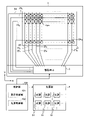
図5は、表示部2、光源部6、導光部7及び拡散板9の態様及び配置を示す図である。以下の説明において、表示部2に照射される光Lの光軸ILに沿う方向をZ方向とする。また、Z方向に直交する平面に沿う2方向の一方をX方向とし、他方向をY方向とする。X方向は、H方向と同一の方向である。Z方向から見た平面視点において、Y方向とV方向とは重なる。実施形態では、光軸ILは、光源61が有する基板612(図14参照)の配置により定められる。具体的には、光源61は、基板612の板面に設けられた発光素子(例えば、発光ダイオード(LED:Light Emitting Diode)61l)から、基板612に直交する方向を光軸ILとして光Lが射出するよう設計されている。すなわち、基板612をX-Y平面に沿うよう配置することで、光軸ILがZ方向に定まる。 FIG. 5 is a diagram showing the mode and arrangement of the display section 2, the light source section 6, the light guide section 7, and the diffusion plate 9. As shown in FIG. In the following description, the direction along the optical axis IL of the light L with which the display section 2 is irradiated is defined as the Z direction. One of two directions along a plane perpendicular to the Z direction is defined as the X direction, and the other direction is defined as the Y direction. The X direction is the same direction as the H direction. The Y direction and the V direction overlap in a planar viewpoint viewed from the Z direction. In the embodiment, the optical axis IL is defined by the placement of the substrate 612 (see FIG. 14) that the light source 61 has. Specifically, the light source 61 emits light L from a light emitting element (for example, a light emitting diode (LED: Light Emitting Diode) 61l) provided on the plate surface of the substrate 612, with an optical axis IL extending in a direction orthogonal to the substrate 612. Designed to shoot. That is, by arranging the substrate 612 along the XY plane, the optical axis IL is determined in the Z direction.
実施形態の表示装置1は、リフレクターユニットRUとして機能する導光部7を備える。導光部7は、複数の導光部材700を有する。導光部材700は、リフレクターRとして機能する。すなわち、導光部材700は、光源61から表示部2に向かって延出して光源61からの光Lの光軸ILの周囲を覆う筒状の部材として設けられる。導光部材700は、光源61からの光Lを内面で反射して表示部側に導く。図5では、光源61から発せられた光の出射口の縁が形成する出射面701に沿って並ぶ4つの導光部材700を例示している。図5等では、配置が異なる当該4つの導光部材700を区別する目的で、導光部材711,721,731,741のように導光部材700の列毎に符号を異ならせている。出射面701は、第1方向Iaに沿っている。第1方向Iaは、Y方向に対して傾斜する。光源61は、導光部材700の一端に配置されている。導光部材700の一端とは、出射面701の反対側の端部である。以下、導光部材700の他端と記載した場合、出射面701側の端部をさす。光源61が配置された導光部材700の一端は、X-Y平面に沿う。なお、光源61は、光源LMとして機能する。また、表示部2は、表示パネルPとして機能する。 The display device 1 of the embodiment includes a light guide section 7 functioning as a reflector unit RU. The light guide section 7 has a plurality of light guide members 700 . The light guide member 700 functions as a reflector R. That is, the light guide member 700 is provided as a tubular member that extends from the light source 61 toward the display section 2 and covers the periphery of the optical axis IL of the light L from the light source 61 . The light guide member 700 reflects the light L from the light source 61 on its inner surface and guides it to the display unit side. FIG. 5 illustrates four light guide members 700 arranged along an emission surface 701 formed by the edge of the emission port for light emitted from the light source 61 . In FIG. 5 and the like, for the purpose of distinguishing the four light guide members 700 having different arrangements, the reference numerals are different for each row of the light guide members 700, such as light guide members 711, 721, 731, and 741. FIG. The exit surface 701 extends along the first direction Ia. The first direction Ia is inclined with respect to the Y direction. The light source 61 is arranged at one end of the light guide member 700 . One end of the light guide member 700 is the end opposite to the exit surface 701 . Hereinafter, when the other end of the light guide member 700 is described, it means the end on the exit surface 701 side. One end of the light guide member 700 where the light source 61 is arranged extends along the XY plane. Note that the light source 61 functions as a light source LM. The display unit 2 also functions as a display panel P. As shown in FIG.
導光部7の一端側は、第1方向Iaに沿って並ぶ複数の導光部材700の一端側が階段状の段差を形成している。図5では、導光部材711,721,731,741の順で、第1方向Iaに沿って並ぶ導光部材700の一端の位置が光源61の光の出射方向(上)側、すなわち他端側にずれている。すなわち、導光部材721の一端及び導光部材721に設けられた光源61は、導光部材711の一端及び導光部材711に設けられた光源61よりも他端側に位置する。導光部材731の一端及び導光部材731に設けられた光源61は、導光部材721の一端及び導光部材721に設けられた光源61よりも他端側に位置する。導光部材741の一端及び導光部材741に設けられた光源61は、導光部材731の一端及び導光部材731に設けられた光源61よりも他端側に位置する。 At one end side of the light guide portion 7, one end sides of the plurality of light guide members 700 arranged along the first direction Ia form a stepped step. In FIG. 5, the light guide members 711, 721, 731, and 741 are arranged in this order along the first direction Ia. shifted to the side. That is, one end of the light guide member 721 and the light source 61 provided on the light guide member 721 are positioned closer to the other end than one end of the light guide member 711 and the light source 61 provided on the light guide member 711 . One end of the light guide member 731 and the light source 61 provided on the light guide member 731 are positioned closer to the other end than one end of the light guide member 721 and the light source 61 provided on the light guide member 721 . One end of the light guide member 741 and the light source 61 provided on the light guide member 741 are positioned closer to the other end than one end of the light guide member 731 and the light source 61 provided on the light guide member 731 .
導光部7の一端側には、電力供給ユニット62が設けられている。電力供給ユニット62の導光部7側には、上述のように階段状の段差を形成するよう配置された複数の光源LMに対応する階段状の段差が形成されている。複数の導光部材700の各々の一端側に設けられた複数の光源61は、電力供給ユニット62の導光部7側の面と接続することで電力供給ユニット62からの電力の供給及び制御部100からの光量の制御を受ける。なお、図5では、電力供給ユニット62と導光部7との間に隙間があるが、実際には当該隙間はない。すなわち、複数の導光部材700の各々の一端側に設けられた複数の光源61は、電力供給ユニット62の導光部7側の段のいずれかに配置されている。各段の導光部7側の面である第1段611、第2段621、第3段631及び第4段641の導光部7側の面は、X-Y平面に沿う。第1段611には、導光部材711に設けられた光源61が載置される。第2段621には、導光部材721に設けられた光源61が載置される。第3段631には、導光部材731に設けられた光源61が載置される。第4段641には、導光部材741に設けられた光源61が載置される。 A power supply unit 62 is provided on one end side of the light guide section 7 . On the light guide portion 7 side of the power supply unit 62, stepped steps corresponding to the plurality of light sources LM arranged to form stepped steps as described above are formed. The plurality of light sources 61 provided on one end side of each of the plurality of light guide members 700 are connected to the surface of the power supply unit 62 on the side of the light guide section 7, thereby supplying power from the power supply unit 62 and controlling the power supply. 100 controls the amount of light. Although there is a gap between the power supply unit 62 and the light guide section 7 in FIG. 5, there is no such gap in practice. That is, the plurality of light sources 61 provided on one end side of each of the plurality of light guide members 700 are arranged in one of the steps of the power supply unit 62 on the light guide section 7 side. The surfaces of the first step 611, the second step 621, the third step 631, and the fourth step 641, which are the surfaces of the steps facing the light guide portion 7, extend along the XY plane. The light source 61 provided on the light guide member 711 is placed on the first stage 611 . The light source 61 provided on the light guide member 721 is placed on the second stage 621 . The light source 61 provided on the light guide member 731 is placed on the third stage 631 . The light source 61 provided on the light guide member 741 is placed on the fourth stage 641 .
導光部7の出射面701側には、表示部2及び拡散板9が配置されている。拡散板9は、表示部2と導光部7との間に介在する。表示部2の板面201は、第2方向Ibに沿っている。拡散板9の板面901は、第3方向Icに沿っている。第2方向Ib及び第3方向Icは、Y方向に対して傾斜する。実施形態では、第1方向Ia、第2方向Ib及び第3方向IcのY方向に対する傾斜方向及び傾斜角度は同じである。第1方向Ia、第2方向Ib及び第3方向Icの少なくとも1つは、他の1つと異なってもよい。ただし、第2方向IbのY方向に対する傾斜角度と第3方向IcのY方向に対する傾斜角度との差は±2%の範囲内であることが望ましい。この「2%」は、一方(第2方向IbのY方向に対する傾斜角度又は第3方向IcのY方向に対する傾斜角度)を100%とした場合の他方の比率である。 The display section 2 and the diffuser plate 9 are arranged on the exit surface 701 side of the light guide section 7 . The diffusion plate 9 is interposed between the display section 2 and the light guide section 7 . A plate surface 201 of the display unit 2 extends along the second direction Ib. A plate surface 901 of the diffuser plate 9 extends along the third direction Ic. The second direction Ib and the third direction Ic are inclined with respect to the Y direction. In the embodiment, the first direction Ia, the second direction Ib and the third direction Ic have the same inclination direction and inclination angle with respect to the Y direction. At least one of the first direction Ia, the second direction Ib and the third direction Ic may be different from the other one. However, the difference between the inclination angle of the second direction Ib with respect to the Y direction and the inclination angle of the third direction Ic with respect to the Y direction is preferably within a range of ±2%. This "2%" is the ratio of the other (the angle of inclination of the second direction Ib with respect to the Y direction or the angle of inclination of the third direction Ic with respect to the Y direction) to 100%.
図6は、導光部7の斜視図である。図7は、導光部7のX-Z平面図である。導光部7は、X方向に沿って並ぶ複数の導光部材700を有する。図6及び図7では、導光部材711,712,713,714,715,716,717,718のようにX方向に並ぶ8つの導光部材700が形成する導光部材700の行を例示している。導光部材711と異なる列の導光部材721,731,741の各々の位置でも、導光部材721,…,728、導光部材731,…,738、導光部材741,…,748のように、X方向に並ぶ8つの導光部材700が、導光部材700の行を形成している。X方向に沿って並ぶ導光部材700の数は7つ以下であってもよいし、9つ以上であってもよい。同様に、第1方向Iaに沿って並ぶ導光部材700の数は3つ以下であってもよいし、5つ以上であってもよい。光源61の数及び配置は、導光部材700の数及び配置に対応する。 FIG. 6 is a perspective view of the light guide section 7. FIG. 7 is an XZ plan view of the light guide section 7. FIG. The light guide section 7 has a plurality of light guide members 700 arranged along the X direction. 6 and 7 illustrate rows of light guide members 700 formed by eight light guide members 700 arranged in the X direction, such as light guide members 711, 712, 713, 714, 715, 716, 717, and 718. ing. , 728, light guide members 731, . . . , 738, and light guide members 741, . In addition, eight light guide members 700 aligned in the X direction form a row of light guide members 700 . The number of light guide members 700 arranged along the X direction may be seven or less, or may be nine or more. Similarly, the number of light guide members 700 arranged along the first direction Ia may be three or less, or may be five or more. The number and arrangement of light sources 61 correspond to the number and arrangement of light guide members 700 .
図5を参照して説明した出射面701は、行列方向に並ぶ複数の導光部材700の他端の縁に沿う面である(図6及び図7参照)。上述のように、出射面701は第1方向Iaに沿い、Y方向に対して傾斜している。図6では、第1方向IaのY方向に対する傾斜角度を角度θaとしている。角度θaは、例えば13°であるが、この角度は一例であってこれに限られるものでなく、適宜変更可能である。 The exit surface 701 described with reference to FIG. 5 is a surface along the edges of the other ends of the plurality of light guide members 700 arranged in the matrix direction (see FIGS. 6 and 7). As described above, the exit surface 701 is inclined with respect to the Y direction along the first direction Ia. In FIG. 6, the inclination angle of the first direction Ia with respect to the Y direction is the angle θa. The angle θa is, for example, 13°, but this angle is an example and is not limited to this, and can be changed as appropriate.
図8は、導光部7のX-Y平面図である。図9は、図8のJ-J断面図である。J-J断面は、導光部材721,…,728が形成する導光部材700の行のX-Z断面であるが、他の導光部材700の行のX-Z断面も同様である。図10は、図8のK-K断面図である。K-K断面は、導光部材714,…,744が形成する導光部材700の列のY-Z断面であるが、他の導光部材700の列のY-Z断面も同様である。 FIG. 8 is an XY plan view of the light guide section 7. FIG. FIG. 9 is a cross-sectional view along JJ in FIG. The JJ cross section is the XZ cross section of the row of the light guide members 700 formed by the light guide members 721, . 10 is a cross-sectional view taken along line KK of FIG. 8. FIG. The KK cross section is the YZ cross section of the row of the light guide members 700 formed by the light guide members 714, .
導光部材700は、反射部750を有する。反射部750は、導光部材700が形成する筒の内面を被覆する。反射部750は、光源61からの光Lの反射率をより高めるために設けられる。反射部750は、実施形態における導光部材700の素材である樹脂よりも光Lの反射率が高い部材であればよい。例えば、反射部750は、導光部材700の内面に貼り付けられたシート状の反射部材であってもよいし、導光部材700の内面に塗布、蒸着等の方法で固着された金属又は化合物であってもよいし、他の方法で導光部材700の内側に設けられた部材であってもよい。 The light guide member 700 has a reflecting portion 750 . The reflecting portion 750 covers the inner surface of the cylinder formed by the light guide member 700 . The reflecting portion 750 is provided to further increase the reflectance of the light L from the light source 61 . The reflecting portion 750 may be a member having a higher reflectance of the light L than the resin that is the material of the light guide member 700 in the embodiment. For example, the reflective part 750 may be a sheet-like reflective member attached to the inner surface of the light guide member 700, or may be a metal or compound adhered to the inner surface of the light guide member 700 by a method such as coating or vapor deposition. or a member provided inside the light guide member 700 by another method.
反射部750は、Y方向に対向する第1内面部751と第2内面部752及びX方向に対向する第3内面部753と第4内面部754を含む。第2内面部752は、第1内面部751に比してZ方向の延設長が長い。第1内面部751と第2内面部752のZ方向の延設長の差は、第2内面部752側から第1内面部751に向かって上る方向の第1方向Iaに対応して決定される。第3内面部753と第4内面部754は、Y方向に線対称である。すなわち、第3内面部753の一端側と第4内面部754の一端側とを結ぶ直線は、X方向に沿う。また、第3内面部753の他端側と第4内面部754の他端側とを結ぶ直線は、X方向に沿う。また、第1内面部751の他端側と第2内面部752の他端側とを結ぶ直線は、X方向に沿う。 The reflector 750 includes a first inner surface portion 751 and a second inner surface portion 752 facing each other in the Y direction, and a third inner surface portion 753 and a fourth inner surface portion 754 facing each other in the X direction. The second inner surface portion 752 has a longer extension length in the Z direction than the first inner surface portion 751 . The difference in the extension length in the Z direction between the first inner surface portion 751 and the second inner surface portion 752 is determined corresponding to the first direction Ia, which is the upward direction from the second inner surface portion 752 side toward the first inner surface portion 751 . be. The third inner surface portion 753 and the fourth inner surface portion 754 are line-symmetrical in the Y direction. That is, a straight line connecting one end side of the third inner surface portion 753 and one end side of the fourth inner surface portion 754 extends along the X direction. A straight line connecting the other end side of the third inner surface portion 753 and the other end side of the fourth inner surface portion 754 extends along the X direction. A straight line connecting the other end side of the first inner surface portion 751 and the other end side of the second inner surface portion 752 extends along the X direction.
実施形態における第1内面部751と第2内面部752との継目、第2内面部752と第3内面部753との継目、第3内面部753と第4内面部754との継目及び第4内面部754と第1内面部751との継目は湾曲形状であるが、角を形成する継目であってもよく、具体的形状は適宜変更可能である。これらの継目の外周側に位置する導光部材700の形状も同様である。 In the embodiment, the joint between the first inner surface portion 751 and the second inner surface portion 752, the joint between the second inner surface portion 752 and the third inner surface portion 753, the joint between the third inner surface portion 753 and the fourth inner surface portion 754, and the fourth The joint between the inner surface portion 754 and the first inner surface portion 751 has a curved shape, but it may be a joint forming an angle, and the specific shape can be changed as appropriate. The shape of the light guide member 700 located on the outer peripheral side of these joints is the same.
実施形態では、導光部材700の素材である樹脂は、黒色の樹脂である。黒色の樹脂は、他の色の樹脂に比して光を吸収しやすい。このため、光源61からの光Lが導光部材700を透過して外部に漏れることを抑制することができる。 In the embodiment, the resin that is the material of the light guide member 700 is black resin. Black resin absorbs light more easily than resins of other colors. Therefore, it is possible to prevent the light L from the light source 61 from transmitting through the light guide member 700 and leaking to the outside.
導光部材700は、底部Bから先端部Tに向かって末広がりの形状を有する。すなわち、導光部材700は、内面と光軸ILとの距離が光源61側(一端側)から出射面701側(他端側)に向かって大きくなる形状を有する。これは、光源61からの光Lの光の反射方向をよりZ方向に沿わせるための形状として機能することに加え、導光部材700を射出成形する場合の抜き勾配としても利用可能である。また、導光部材700の筒を形成する壁面のうち、相対的に他端側に位置する先端部Tの厚みは、相対的に一端側に位置する底部Bの厚みよりも薄い。これによって、底部Bに比して大きな筒状の枠体として形成される先端部Tにヒケが生じる可能性をより低減することができる。 The light guide member 700 has a shape that widens from the bottom portion B toward the tip portion T. As shown in FIG. That is, the light guide member 700 has a shape in which the distance between the inner surface and the optical axis IL increases from the light source 61 side (one end side) toward the emission surface 701 side (the other end side). In addition to functioning as a shape for making the reflection direction of the light L from the light source 61 more along the Z direction, this can also be used as a draft angle when the light guide member 700 is injection molded. Further, among the wall surfaces forming the cylinder of the light guide member 700, the thickness of the tip portion T relatively located on the other end side is thinner than the thickness of the bottom portion B relatively located on the one end side. As a result, the possibility of sink marks occurring in the tip portion T, which is formed as a cylindrical frame that is larger than the bottom portion B, can be further reduced.
図11は、導光部材700のY-Z平面図である。図12及び図13は、導光部材700のX-Z平面図である。導光部材700は、Y方向に対向する第1壁面部761と第2壁面部762及びX方向に対向する第3壁面部763と第4壁面部764を含む。第2内面部752と第1内面部751との関係と同様、第2壁面部762のZ方向の延設長Z2は、第1壁面部761のZ方向の延設長Z1に比して長い。第1壁面部761と第2壁面部762のZ方向の延設長の差は、第1方向Iaに対応して決定される。第3壁面部763と第4壁面部764は、第3内面部753と第4内面部754との関係と同様、Y方向に線対称である。すなわち、第3壁面部763の一端側と第4壁面部764の一端側とを結ぶ直線は、X方向に沿う。また、第1壁面部761の一端側と第2壁面部762の一端側とを結ぶ直線は、X方向に沿う。すなわち、上述のように、導光部材700の一端側は、X-Y平面に沿う。また、第3壁面部763の他端側と第4壁面部764の他端側とを結ぶ直線は、X方向に沿う。なお、図12は、第1壁面部761側から見た図である。また、図13は、第2壁面部762側から見た図である。 11 is a YZ plan view of the light guide member 700. FIG. 12 and 13 are XZ plan views of the light guide member 700. FIG. The light guide member 700 includes a first wall surface portion 761 and a second wall surface portion 762 facing in the Y direction, and a third wall surface portion 763 and a fourth wall surface portion 764 facing in the X direction. Similarly to the relationship between the second inner surface portion 752 and the first inner surface portion 751, the extending length Z2 of the second wall surface portion 762 in the Z direction is longer than the extending length Z1 of the first wall surface portion 761 in the Z direction. . The difference in the extension length in the Z direction between the first wall surface portion 761 and the second wall surface portion 762 is determined corresponding to the first direction Ia. The third wall surface portion 763 and the fourth wall surface portion 764 are line-symmetrical in the Y direction, similar to the relationship between the third inner surface portion 753 and the fourth inner surface portion 754 . That is, a straight line connecting one end side of the third wall surface portion 763 and one end side of the fourth wall surface portion 764 extends along the X direction. A straight line connecting one end side of the first wall surface portion 761 and one end side of the second wall surface portion 762 extends along the X direction. That is, as described above, one end side of the light guide member 700 extends along the XY plane. A straight line connecting the other end side of the third wall surface portion 763 and the other end side of the fourth wall surface portion 764 extends along the X direction. In addition, FIG. 12 is a view seen from the first wall surface portion 761 side. 13 is a view seen from the second wall surface portion 762 side.
図11における第1壁面部761の第1中間部P3と、第2壁面部762の第1中間部P4とは、光軸ILに対する距離が同じである。一方、導光部材700の一端と第1中間部P3とのZ方向の間隔Z3と、導光部材700の一端と第1中間部P3とのZ方向の間隔Z4とは異なる。図11では、Z4>Z3である。このため、第3壁面部763上に第1中間部P3と第1中間部P4とを結ぶ線を描いた場合、Z方向に対して第1方向Iaと同じ方向の傾斜を有する線になる。これは、導光部材700の一端側から他端側に向かって末広がりになる形状の曲率が、第1壁面部761と第2壁面部762とで異なることを示す。第1壁面部761の第2中間部P5と第2壁面部762の第2中間部P5との関係及び第1壁面部761の第3中間部P7と第2壁面部762の第3中間部P8との関係も、第1中間部P3と第1中間部P4の関係と同様である。このように、導光部材700は、光軸ILに直交する位置で対向する部分の曲率が均一でない。 The first intermediate portion P3 of the first wall surface portion 761 and the first intermediate portion P4 of the second wall surface portion 762 in FIG. 11 have the same distance from the optical axis IL. On the other hand, the Z-direction spacing Z3 between one end of the light guide member 700 and the first intermediate portion P3 is different from the Z-direction spacing Z4 between one end of the light guide member 700 and the first intermediate portion P3. In FIG. 11, Z4>Z3. Therefore, when a line connecting the first intermediate portion P3 and the first intermediate portion P4 is drawn on the third wall surface portion 763, the line is inclined with respect to the Z direction in the same direction as the first direction Ia. This indicates that the first wall surface portion 761 and the second wall surface portion 762 have different curvatures in the shape of the light guide member 700 that widens from one end side to the other end side. The relationship between the second intermediate portion P5 of the first wall surface portion 761 and the second intermediate portion P5 of the second wall surface portion 762, and the third intermediate portion P7 of the first wall surface portion 761 and the third intermediate portion P8 of the second wall surface portion 762 is the same as the relationship between the first intermediate portion P3 and the first intermediate portion P4. As described above, the light guide member 700 has uneven curvatures in the portions facing each other at a position perpendicular to the optical axis IL.
導光部材700の内面に設けられる反射部750も、導光部材700と同様、光軸ILに直交する位置で対向する内面の曲率の不均一による曲率の差を有する。係る曲率の差は、一端-他端間の距離が第1内面部751と第2内面部752で異なることによる光Lの反射の差異を低減するように設けられる。すなわち、光軸ILを挟んで第1内面部751側と第2内面部752側で出射口から発せられる光Lの輝度分布がより均一に近づくように曲率の差が設けられる。 Similarly to the light guide member 700, the reflecting portion 750 provided on the inner surface of the light guide member 700 also has a difference in curvature due to non-uniform curvatures of the opposing inner surfaces at positions perpendicular to the optical axis IL. The difference in curvature is provided so as to reduce the difference in reflection of the light L due to the difference in the distance between the first inner surface portion 751 and the second inner surface portion 752 . In other words, a difference in curvature is provided between the first inner surface portion 751 side and the second inner surface portion 752 side with the optical axis IL therebetween so that the luminance distribution of the light L emitted from the exit port becomes more uniform.
なお、第1壁面部761の他端P1と、第2壁面部762の他端P2とは、光軸ILに対する距離が等しい必要はない。光軸ILは、第1壁面部761、第2壁面部762、第3壁面部763及び第4壁面部764の内面、すなわち、第1内面部751、第2内面部752、第3内面部753及び第4内面部754で囲まれる導光部材700の他端の出射口の中心からY方向にずれた位置であってもよい。例えば、光軸ILは、Z方向に沿う線であって、他端P1と他端P2に対するY方向の距離が等しい線(中間線)よりも第1内面部751側にずれていてもよい。なお、X方向については、光軸ILは、第3内面部753と第4内面部754とが線対称の関係になる線上に位置することが望ましい。 The other end P1 of the first wall surface portion 761 and the other end P2 of the second wall surface portion 762 do not need to have the same distance from the optical axis IL. The optical axis IL extends along the inner surfaces of the first wall surface portion 761, the second wall surface portion 762, the third wall surface portion 763, and the fourth wall surface portion 764, that is, the first inner surface portion 751, the second inner surface portion 752, and the third inner surface portion 753. and the position shifted in the Y direction from the center of the exit opening at the other end of the light guide member 700 surrounded by the fourth inner surface portion 754 . For example, the optical axis IL may be shifted toward the first inner surface portion 751 from a line (intermediate line) that is a line along the Z direction and has the same distance in the Y direction from the other end P1 and the other end P2. In the X direction, it is desirable that the optical axis IL be positioned on a line that makes the third inner surface portion 753 and the fourth inner surface portion 754 symmetrical.
図14は、光源61の斜視図である。光源61は、LED61lと、基板612と、拡散部材613とを有する。LED61lは、例えば白色の光を発する発光ダイオードである。LED61lは、電力供給ユニット62から供給される電力によって点灯し、光を発する。基板612は、LED61lに接続される配線が実装された基板である。基板612は、電力供給ユニット62の段のいずれかに載置されてLED61lと電力供給ユニット62とを接続する。導光部材700の一端と他端の位置関係を基準にすると、基板612は、LED61lの一端側に位置する。LED61lは、他端側に光を発する。拡散部材613は、LED61l及び基板612の他端側を覆うように設けられて透光性を有する導光材であり、拡散板9と同様の構成である。拡散部材613は、LED61lからの光を面状に拡散させて他端側から出射する。 14 is a perspective view of the light source 61. FIG. The light source 61 has an LED 61 l, a substrate 612 and a diffusion member 613 . The LED 61l is, for example, a light emitting diode that emits white light. The LED 61l is lit by power supplied from the power supply unit 62 and emits light. The substrate 612 is a substrate on which wiring connected to the LED 61l is mounted. The board 612 is mounted on one of the stages of the power supply unit 62 to connect the LED 61l and the power supply unit 62 . Based on the positional relationship between one end and the other end of the light guide member 700, the substrate 612 is located on the one end side of the LED 61l. The LED 61l emits light to the other end side. The diffusing member 613 is a translucent light guiding member provided to cover the other end side of the LED 61 l and the substrate 612 , and has the same configuration as the diffusing plate 9 . The diffusion member 613 planarly diffuses the light from the LED 61l and emits it from the other end side.
実施形態では、基板612及び拡散部材613のX-Y平面形状は、X方向に沿って対向する2辺とY方向に沿って対向する他の2辺とを含む4辺を有する矩形状である。導光部材700の一端における筒の内側の形状は、光源61のX-Y平面形状の外形に対応する。このように、光源61は、矩形状の発光面を有する。また、導光部材700は、X-Y平面に沿う形状が当該発光面の四辺に沿う四辺(第1壁面部761、第2壁面部762、第3壁面部763、第4壁面部764)を有する形状である(図8参照)。 In the embodiment, the XY plane shape of the substrate 612 and the diffusion member 613 is a rectangular shape having four sides including two sides facing each other along the X direction and other two sides facing each other along the Y direction. . The inner shape of the tube at one end of the light guide member 700 corresponds to the outer shape of the light source 61 in the XY plane. Thus, the light source 61 has a rectangular light emitting surface. In addition, the light guide member 700 has a shape along the XY plane that extends along the four sides of the light emitting surface (the first wall surface portion 761, the second wall surface portion 762, the third wall surface portion 763, and the fourth wall surface portion 764). It has a shape (see FIG. 8).
また、実施形態の基板612は、少なくとも他端側が黒色の基板である。すなわち、基板612は、少なくともLED61lが設けられている側の色が黒色である。このため、LED61lからの光軸ILが基板612を透過して一端側に漏れることを抑制することができる。基板612は、配線パターン等が積層される前の他端側の面が黒色であるだけでもよいし、一端側の面を含むより多くの範囲が黒色であってもよい。 Further, the substrate 612 of the embodiment is a substrate having at least the other end side in black. That is, the color of the substrate 612 is black at least on the side where the LED 61l is provided. Therefore, it is possible to prevent the optical axis IL from the LED 61l from passing through the substrate 612 and leaking to the one end side. The substrate 612 may be black only on the surface on the other end side before the wiring pattern or the like is laminated, or may be black on a wider range including the surface on the one end side.
図14では、1つの光源61に設けられたLED61lが1つであるが、1つの光源61に複数のLED61lが設けられてもよい。 In FIG. 14, one light source 61 is provided with one LED 61l, but one light source 61 may be provided with a plurality of LEDs 61l.
以下、実施形態の作用効果について、図15を参照して説明する。図15は、表示部2の板面201、出射面701及び拡散板9の板面901の角度と、表示装置が出力する画像の形状及び輝度分布との関係を示す模式的な説明図である。 The effects of the embodiment will be described below with reference to FIG. 15 . FIG. 15 is a schematic explanatory diagram showing the relationship between the angles of the plate surface 201 of the display unit 2, the emission surface 701, and the plate surface 901 of the diffusion plate 9, and the shape and luminance distribution of an image output by the display device. .
図15の実施例では、上述の実施形態のように、出射面701、板面201、板面901がそれぞれY方向に対して傾斜する第1方向Ia、第2方向Ib、第3方向Icを与えられた状態で設けられている。このような実施例では、画像VIは、全体的に明るさの偏りが特段生じない矩形の画像として視認される。 In the example of FIG. 15, the output surface 701, the plate surface 201, and the plate surface 901 tilt in the first direction Ia, the second direction Ib, and the third direction Ic with respect to the Y direction, respectively, as in the above-described embodiment. provided as given. In such an embodiment, the image VI is visually recognized as a rectangular image with no particular unevenness in brightness as a whole.
一方、図15の比較例1では、板面201のみがY方向に対して傾斜する第2方向Ibを与えられ、出射面701及び板面901がY方向に沿うよう設けられている。このような比較例1では、画像VIは、板面201と板面901との距離が相対的に近い側に対応する画像の一辺が相対的に短く、板面201と板面901との距離が相対的に遠い側の対向辺が相対的に長い台形状の画像として視認される。すなわち、比較例1では、画像に歪みが生じる。 On the other hand, in Comparative Example 1 of FIG. 15, only the plate surface 201 is given the second direction Ib inclined with respect to the Y direction, and the output surface 701 and the plate surface 901 are provided along the Y direction. In Comparative Example 1 as described above, in the image VI, one side of the image corresponding to the side where the distance between the plate surface 201 and the plate surface 901 is relatively short is relatively short, and the distance between the plate surface 201 and the plate surface 901 is relatively short. is viewed as a trapezoidal image in which the opposite side on the side farther from is relatively long. That is, in Comparative Example 1, the image is distorted.
また、図15の比較例2では、板面201がY方向に対して傾斜する第2方向Ibを与えられ、板面901がY方向に対して傾斜する第3方向Icを与えられ、出射面701がY方向に沿うよう設けられている。このような比較例2では、画像VIは、板面201と出射面701との距離が相対的に近い側に対応する画像の一辺側が相対的に明るく、板面201と出射面701との距離が相対的に遠い側の対向辺側が相対的に暗い画像として視認される。すなわち、比較例1では、画像の明るさに偏りが生じる。 In Comparative Example 2 of FIG. 15, the plate surface 201 is given the second direction Ib inclined with respect to the Y direction, and the plate surface 901 is given the third direction Ic inclined with respect to the Y direction. 701 is provided along the Y direction. In Comparative Example 2, the image VI is relatively bright on one side of the image corresponding to the side where the distance between the plate surface 201 and the exit surface 701 is relatively short, and the distance between the plate surface 201 and the exit surface 701 is relatively bright. is viewed as a relatively dark image. That is, in Comparative Example 1, the brightness of the image is uneven.
なお、上述のように、導光部材700は、光軸ILに直交する位置で対向する内面の曲率が均一でない。この影響で、出射面701のY方向の中間線上に光軸が位置すると、輝度の偏りが生じる。具体的には、光軸ILを挟んで第1壁面部761側から発せられる光の輝度が、第2壁面部762側から発せられる光の輝度に比して有意に高くなる。当該中間線に対して第2壁面部762側の位置(図11の左側)に光軸ILが位置する場合にも、同様の輝度の偏りが生じる。 As described above, the light guide member 700 has non-uniform curvatures on the inner surfaces facing each other at a position perpendicular to the optical axis IL. Due to this effect, if the optical axis is positioned on the middle line of the exit surface 701 in the Y direction, the luminance will be uneven. Specifically, the brightness of the light emitted from the first wall surface portion 761 side across the optical axis IL is significantly higher than the brightness of the light emitted from the second wall surface portion 762 side. When the optical axis IL is positioned on the second wall surface portion 762 side (left side in FIG. 11) with respect to the intermediate line, a similar bias in luminance occurs.
そこで、光軸ILの位置を当該中間線に対して第1壁面部761側(図11の右側)にずらすことで、輝度の偏りの発生を抑制することができる。言い換えれば、光軸ILの位置を、中間線を挟んで他端P1側(図11の右側)にずらすことで、輝度の偏りの発生を抑制することができる。 Therefore, by shifting the position of the optical axis IL toward the first wall surface portion 761 (to the right in FIG. 11) with respect to the intermediate line, it is possible to suppress the unevenness of luminance. In other words, by shifting the position of the optical axis IL to the other end P1 side (to the right side in FIG. 11) across the intermediate line, it is possible to suppress the occurrence of uneven brightness.
以上、実施形態によれば、表示部2の板面201がX-Y平面に対して傾斜している。このため、光源からの光と反射光とが重複して多重投影されることによるゴーストの発生を抑制することができる。また、導光部7の出射面701がX-Y平面に対して傾斜している。また、Z方向に沿う光軸ILに対する板面201の傾斜方向と出射面701の傾斜方向が同じである。このため、全体的に明るさの偏りが特段生じない矩形の画像として視認される画像VIを得ることができる。従って、実施形態によれば、ゴーストの抑制と画質とを両立することができる。 As described above, according to the embodiment, the plate surface 201 of the display section 2 is inclined with respect to the XY plane. Therefore, it is possible to suppress the occurrence of a ghost due to overlapping and multiple projection of the light from the light source and the reflected light. In addition, the exit surface 701 of the light guide section 7 is inclined with respect to the XY plane. In addition, the tilt direction of the plate surface 201 and the tilt direction of the output surface 701 with respect to the optical axis IL along the Z direction are the same. For this reason, it is possible to obtain an image VI that is visually recognized as a rectangular image in which there is no particular unevenness in brightness as a whole. Therefore, according to the embodiment, it is possible to achieve both ghost suppression and image quality.
また、導光部材700は、内面と光軸ILとの距離が光源61側から出射面701側に向かって大きくなる末広がりの形状を有し、光軸ILに直交する位置で対向する内面の曲率が均一でない。このため、一端-他端間の距離が第1内面部751と第2内面部752で異なることによる光Lの反射の差異を、曲率の差異によって低減することができる。 In addition, the light guide member 700 has a shape that widens toward the output surface 701 so that the distance between the inner surface and the optical axis IL increases. is not uniform. Therefore, the difference in reflection of the light L due to the difference in the distance between one end and the other end between the first inner surface portion 751 and the second inner surface portion 752 can be reduced by the difference in curvature.
また、光軸ILは、中間線から所定方向にずれている。ここで、所定方向は、中間線を挟んで他端P1側と他端P2側のうち、第1方向Iaによって出射口の縁と光源61との距離が相対的に短くなっている他端P1側に向かう方向(図11の右側)である。これによって、一端-他端間の距離が第1内面部751と第2内面部752で異なることによる光Lの反射の差異をより低減することができる。 Also, the optical axis IL is shifted in a predetermined direction from the intermediate line. Here, the predetermined direction is the other end P1 side where the distance between the edge of the emission port and the light source 61 is relatively short due to the first direction Ia, out of the other end P1 side and the other end P2 side across the intermediate line. the direction toward the side (right side in FIG. 11). As a result, the difference in reflection of the light L due to the difference in distance between one end and the other end between the first inner surface portion 751 and the second inner surface portion 752 can be further reduced.
また、光源61は、矩形状の発光面を有する。また、導光部材700は、X-Y平面に沿う形状が発光面の四辺に沿う四辺を有する形状である。これによって、矩形状の表示領域21を有する表示部2を照明するのにより好適な光源部6を得ることができる。 Moreover, the light source 61 has a rectangular light emitting surface. Further, the light guide member 700 has a shape along the XY plane with four sides along the four sides of the light emitting surface. This makes it possible to obtain the light source unit 6 more suitable for illuminating the display unit 2 having the rectangular display area 21 .
また、光源61及び導光部材700は複数設けられる。導光部材700は、光源61毎に個別に設けられる。また、第1方向Iaに沿って並ぶ複数の光源61は階段状に配置される。これによって、光源61からの光Lの出射面をX-Y平面に沿わせて光軸ILをZ方向に沿わせることと、第1方向Iaに沿う複数の光源61の配置とを両立することができる。また、第1方向Iaに沿う方向のローカルディミングのための複数の光源61の配置を実現することができる。 A plurality of light sources 61 and light guide members 700 are provided. The light guide member 700 is individually provided for each light source 61 . Also, the plurality of light sources 61 arranged along the first direction Ia are arranged in a stepped manner. Accordingly, it is possible to make the emission surface of the light L from the light source 61 along the XY plane and the optical axis IL along the Z direction, and to arrange the plurality of light sources 61 along the first direction Ia. can be done. Also, it is possible to realize the arrangement of the plurality of light sources 61 for local dimming in the direction along the first direction Ia.
また、X方向に沿って複数の光源61が並ぶ。これによって、X方向のローカルディミングのための複数の光源61の配置を実現することができる。 A plurality of light sources 61 are arranged along the X direction. Thereby, it is possible to realize the arrangement of the plurality of light sources 61 for local dimming in the X direction.
また、導光部7と表示部2との間に配置されて光を拡散する拡散板9を備える。これによって、表示領域21をより均一に照明することができる。 Further, a diffuser plate 9 is provided between the light guide section 7 and the display section 2 to diffuse light. Thereby, the display area 21 can be illuminated more uniformly.
また、拡散板9は、X-Y平面に対して表示部2と同じ傾斜方向に傾斜する。また、第2方向Ibと第3方向IcのX-Y平面に対する角度差は±2%以内である。これによって、画像VIにおける明るさの偏りの発生をより抑制することができる。 Further, the diffusion plate 9 is inclined in the same inclination direction as the display section 2 with respect to the XY plane. Also, the angle difference with respect to the XY plane between the second direction Ib and the third direction Ic is within ±2%. This makes it possible to further suppress the occurrence of uneven brightness in the image VI.
さらに、導光部材700が黒色の樹脂からなる。このため、光源61からの光Lが導光部材700を透過して外部に漏れる光漏れを抑制することができる。すなわち、光漏れによる画質の低下を抑制することができる。 Furthermore, the light guide member 700 is made of black resin. Therefore, it is possible to suppress light leakage, in which the light L from the light source 61 is transmitted through the light guide member 700 and leaks to the outside. That is, deterioration of image quality due to light leakage can be suppressed.
さらに、導光部材700は、黒色の樹脂よりも光Lの反射率が高い部材で被覆された反射部750を有する。このため、黒色の樹脂による光漏れの抑制と、反射部750による光Lの誘導とを両立することができる。 Furthermore, the light guide member 700 has a reflecting portion 750 coated with a member having a higher reflectance of the light L than black resin. Therefore, both suppression of light leakage by the black resin and guidance of the light L by the reflecting portion 750 can be achieved.
さらに、導光部材700は、先端部Tの厚みが底部Bよりも薄い。これによって、底部Bに比して大きな筒状の枠体として形成される先端部Tにヒケが生じる可能性をより低減することができる。 Further, the light guide member 700 has a thickness of the tip portion T thinner than that of the bottom portion B. As shown in FIG. As a result, the possibility of sink marks occurring in the tip portion T, which is formed as a cylindrical frame that is larger than the bottom portion B, can be further reduced.
さらに、導光部7を構成する複数の導光部材700は、同一形状である。このため、複数の導光部材700を同一の金型等に基づいて製造し、複数の導光部材700を組み合わせることで導光部7を形成することができる。従って、より容易に導光部7を製造可能になる。 Furthermore, the plurality of light guide members 700 forming the light guide section 7 have the same shape. Therefore, the light guide section 7 can be formed by manufacturing the plurality of light guide members 700 based on the same mold or the like and combining the plurality of light guide members 700 . Therefore, the light guide section 7 can be manufactured more easily.
なお、上記の実施形態はあくまで一例であり、本発明の技術的特徴を逸脱しない範囲内において適宜変更可能である。例えば、実施形態の表示部2は、カラー表示可能な表示パネルであるが、モノクロの表示パネルであってもよい。また、実施形態では、光源61及び導光部材700がマトリクス状に配置されているが、X方向又は第1方向Iaの一方に複数の光源61及び導光部材700が配置される構成であってもよいし、光源61及び導光部材700が1つであってもよい。 It should be noted that the above embodiment is merely an example, and can be modified as appropriate without departing from the technical features of the present invention. For example, the display unit 2 of the embodiment is a display panel capable of color display, but it may be a monochrome display panel. Further, in the embodiment, the light sources 61 and the light guide members 700 are arranged in a matrix. Alternatively, one light source 61 and one light guide member 700 may be provided.
また、本実施形態において述べた態様によりもたらされる他の作用効果について本明細書記載から明らかなもの、又は当業者において適宜想到し得るものについては、当然に本発明によりもたらされるものと解される。 In addition, other actions and effects brought about by the aspects described in this embodiment that are clear from the description of the present specification or that can be appropriately conceived by those skilled in the art are naturally understood to be brought about by the present invention. .
1 表示装置
2 表示部
6 光源部
7 導光部
9 拡散板
61 光源
61l LED
612 基板
62 電力供給ユニット
700 導光部材
701 出射面
750 反射部
B 底部
FG フロントガラス
IL 光軸
L 光
M 鏡
SL 外光
T 先端部
VI 画像
1 display device 2 display unit 6 light source unit 7 light guide unit 9 diffusion plate 61 light source 61 l LED
612 substrate 62 power supply unit 700 light guide member 701 exit surface 750 reflector B bottom FG windshield IL optical axis L light M mirror SL external light T tip VI image
Claims (7)
前記光を一面側から受けて他面側に透過可能に設けられた表示パネルと、
前記光源から前記表示パネルの前記一面側に延出して前記光を前記表示パネル側に反射する導光部材とを備え、
前記表示パネルは、前記光の光軸に直交する直交面に対して傾斜し、
前記導光部材は、前記光の出射口に縁取られる出射面が前記直交面に対して傾斜し、
前記光軸に対する前記表示パネルの傾斜方向と前記光軸に対する前記出射面の傾斜方向は同じであり、
前記光軸は、矩形状の前記出射口の中心から所定方向にずれており、
前記所定方向は、前記直交面に沿う方向であって、かつ、前記出射面の前記直交面に対する傾斜によって前記出射口の縁と前記光源との距離が相対的に短くなっている側に向かう方向である
表示装置。 a light source that emits light;
a display panel provided so as to receive the light from one side and transmit the light to the other side;
a light guide member extending from the light source to the one surface side of the display panel and reflecting the light toward the display panel;
the display panel is inclined with respect to an orthogonal plane orthogonal to the optical axis of the light;
the light guide member has an output surface bordered by the light output port inclined with respect to the orthogonal plane;
the tilt direction of the display panel with respect to the optical axis and the tilt direction of the output surface with respect to the optical axis are the same;
the optical axis is deviated in a predetermined direction from the center of the rectangular exit port,
The predetermined direction is a direction along the orthogonal plane and a direction toward the side where the distance between the edge of the exit port and the light source is relatively short due to the inclination of the exit surface with respect to the orthogonal plane. is a display device.
請求項1に記載の表示装置。 The light guide member has a shape in which the distance between the inner surface and the optical axis increases from the light source side toward the one surface side, and the curvature of the inner surface facing at a position orthogonal to the optical axis is not uniform. 1. The display device according to 1.
前記導光部材は、前記直交面に沿う形状が前記発光面の四辺に沿う四辺を有する形状である
請求項1又は2に記載の表示装置。 The light source has a rectangular light emitting surface,
3. The display device according to claim 1, wherein the shape of the light guide member along the orthogonal plane has four sides along the four sides of the light emitting surface.
前記傾斜方向に並ぶ複数の前記光源は、前記傾斜方向に沿って階段状に配置され、
前記導光部材は、前記光源毎に設けられる
請求項1から3のいずれか一項に記載の表示装置。 A plurality of the light sources and the light guide members are provided,
the plurality of light sources arranged in the tilt direction are arranged stepwise along the tilt direction;
The display device according to any one of claims 1 to 3 , wherein the light guide member is provided for each light source.
請求項4に記載の表示装置。 5. The display device according to claim 4 , wherein the plurality of light sources are arranged along a direction orthogonal to the optical axis and the tilt direction.
請求項1から5のいずれか一項に記載の表示装置。 The display device according to any one of claims 1 to 5 , further comprising a diffusion plate arranged between the light guide member and the display panel to diffuse the light.
前記表示パネルの傾斜角度と前記拡散板の傾斜角度の前記直交面に対する角度差は±2%以内である
請求項6に記載の表示装置。 the diffusion plate is inclined in the same inclination direction as the display panel with respect to the orthogonal plane;
7. The display device according to claim 6 , wherein an angle difference between the inclination angle of the display panel and the inclination angle of the diffusion plate with respect to the orthogonal plane is within ±2%.
Priority Applications (4)
| Application Number | Priority Date | Filing Date | Title |
|---|---|---|---|
| JP2018165084A JP7110036B2 (en) | 2018-09-04 | 2018-09-04 | Display device |
| DE112019003884.2T DE112019003884T5 (en) | 2018-09-04 | 2019-08-05 | Display device |
| PCT/JP2019/030750 WO2020049928A1 (en) | 2018-09-04 | 2019-08-05 | Display device |
| US17/189,911 US11347102B2 (en) | 2018-09-04 | 2021-03-02 | Display device |
Applications Claiming Priority (1)
| Application Number | Priority Date | Filing Date | Title |
|---|---|---|---|
| JP2018165084A JP7110036B2 (en) | 2018-09-04 | 2018-09-04 | Display device |
Publications (3)
| Publication Number | Publication Date |
|---|---|
| JP2020038279A JP2020038279A (en) | 2020-03-12 |
| JP2020038279A5 JP2020038279A5 (en) | 2021-10-07 |
| JP7110036B2 true JP7110036B2 (en) | 2022-08-01 |
Family
ID=69722816
Family Applications (1)
| Application Number | Title | Priority Date | Filing Date |
|---|---|---|---|
| JP2018165084A Active JP7110036B2 (en) | 2018-09-04 | 2018-09-04 | Display device |
Country Status (4)
| Country | Link |
|---|---|
| US (1) | US11347102B2 (en) |
| JP (1) | JP7110036B2 (en) |
| DE (1) | DE112019003884T5 (en) |
| WO (1) | WO2020049928A1 (en) |
Families Citing this family (3)
| Publication number | Priority date | Publication date | Assignee | Title |
|---|---|---|---|---|
| JP7110037B2 (en) * | 2018-09-04 | 2022-08-01 | 株式会社ジャパンディスプレイ | Display device |
| JP2022092951A (en) | 2020-12-11 | 2022-06-23 | 株式会社ジャパンディスプレイ | Lighting unit |
| CN114296253B (en) * | 2022-03-09 | 2022-06-28 | 北京谛听视界文化科技有限公司 | Optical imaging structure |
Citations (7)
| Publication number | Priority date | Publication date | Assignee | Title |
|---|---|---|---|---|
| JP2002156916A (en) | 2000-11-20 | 2002-05-31 | Nippon Seiki Co Ltd | Display device |
| JP2004102132A (en) | 2002-09-12 | 2004-04-02 | Olympus Corp | Lighting device and image projection apparatus using same |
| US20080309470A1 (en) | 2004-04-05 | 2008-12-18 | Thomas Kiesewetter | Built-in instrument cluster |
| JP2013156584A (en) | 2012-01-31 | 2013-08-15 | Toshiba Corp | Display apparatus, moving body, and method for mounting display apparatus |
| US20150168717A1 (en) | 2013-12-12 | 2015-06-18 | Au Optronics Corporation | Display module and head up display |
| WO2017169375A1 (en) | 2016-03-29 | 2017-10-05 | 株式会社デンソー | Head-up display device |
| JP2017207624A (en) | 2016-05-18 | 2017-11-24 | 株式会社ジャパンディスプレイ | Display device |
Family Cites Families (8)
| Publication number | Priority date | Publication date | Assignee | Title |
|---|---|---|---|---|
| FR2680860B1 (en) * | 1991-09-02 | 1997-07-04 | Valeo Vision | SUPPORT ELEMENT, PARTICULARLY FOR MOTOR VEHICLE SIGNALING LIGHT AND MANUFACTURING METHOD THEREOF. |
| US6480345B2 (en) * | 2000-06-30 | 2002-11-12 | Ricoh Company, Ltd. | Image magnifying/reducing optical device and manufacturing method thereof |
| US7832878B2 (en) * | 2006-03-06 | 2010-11-16 | Innovations In Optics, Inc. | Light emitting diode projection system |
| JP2014178368A (en) | 2013-03-13 | 2014-09-25 | Japan Display Inc | Display module |
| DE112015004186B4 (en) * | 2014-09-12 | 2022-07-07 | Yazaki Corporation | Face panel, display unit, in-vehicle display device and dashboard |
| JP6283013B2 (en) * | 2015-11-24 | 2018-02-21 | カルソニックカンセイ株式会社 | Lighting structure |
| JP6508125B2 (en) * | 2016-05-18 | 2019-05-08 | 株式会社デンソー | HEAD-UP DISPLAY DEVICE AND IMAGE PROJECTION UNIT |
| EP3575846A1 (en) * | 2018-05-30 | 2019-12-04 | Visteon Global Technologies Inc. | Picture generation unit for head-up display |
-
2018
- 2018-09-04 JP JP2018165084A patent/JP7110036B2/en active Active
-
2019
- 2019-08-05 DE DE112019003884.2T patent/DE112019003884T5/en active Pending
- 2019-08-05 WO PCT/JP2019/030750 patent/WO2020049928A1/en active Application Filing
-
2021
- 2021-03-02 US US17/189,911 patent/US11347102B2/en active Active
Patent Citations (7)
| Publication number | Priority date | Publication date | Assignee | Title |
|---|---|---|---|---|
| JP2002156916A (en) | 2000-11-20 | 2002-05-31 | Nippon Seiki Co Ltd | Display device |
| JP2004102132A (en) | 2002-09-12 | 2004-04-02 | Olympus Corp | Lighting device and image projection apparatus using same |
| US20080309470A1 (en) | 2004-04-05 | 2008-12-18 | Thomas Kiesewetter | Built-in instrument cluster |
| JP2013156584A (en) | 2012-01-31 | 2013-08-15 | Toshiba Corp | Display apparatus, moving body, and method for mounting display apparatus |
| US20150168717A1 (en) | 2013-12-12 | 2015-06-18 | Au Optronics Corporation | Display module and head up display |
| WO2017169375A1 (en) | 2016-03-29 | 2017-10-05 | 株式会社デンソー | Head-up display device |
| JP2017207624A (en) | 2016-05-18 | 2017-11-24 | 株式会社ジャパンディスプレイ | Display device |
Also Published As
| Publication number | Publication date |
|---|---|
| US11347102B2 (en) | 2022-05-31 |
| US20210181579A1 (en) | 2021-06-17 |
| WO2020049928A1 (en) | 2020-03-12 |
| DE112019003884T5 (en) | 2021-04-15 |
| JP2020038279A (en) | 2020-03-12 |
Similar Documents
| Publication | Publication Date | Title |
|---|---|---|
| JP4600269B2 (en) | Liquid crystal display | |
| US10488577B2 (en) | Illumination device and display device | |
| US11347102B2 (en) | Display device | |
| US8421955B2 (en) | Liquid crystal display device | |
| US20090097230A1 (en) | Illumination device and liquid crystal display device | |
| JP4525612B2 (en) | Display device | |
| JP2012150366A (en) | Light guide member and multi-display device including the same | |
| JP4483233B2 (en) | Surface light source and liquid crystal display device | |
| JP2019186060A (en) | Luminaire and display | |
| JP4720207B2 (en) | Liquid crystal display device | |
| JP4780224B2 (en) | Display device | |
| JP4501625B2 (en) | Surface light source and liquid crystal display device | |
| US9418601B2 (en) | Display device with luminance boosting unit | |
| JP7110037B2 (en) | Display device | |
| US11360352B2 (en) | Display panel, display apparatus and display device | |
| US20170316746A1 (en) | Display apparatus and method for driving display apparatus | |
| WO2012056951A1 (en) | Illumination device and display device | |
| JP4635650B2 (en) | Backlight device and liquid crystal display device | |
| JP2009086026A (en) | Electro-optical device and electronic equipment | |
| JP2005031195A (en) | Picture display device | |
| KR100739758B1 (en) | Back light unit for field sequential color LCD | |
| US11935497B2 (en) | Display device | |
| KR102355832B1 (en) | Display Device having Multiple Display Panel | |
| US20230305339A1 (en) | Image output panel and head-up display | |
| JP5397334B2 (en) | Driving method of display device |
Legal Events
| Date | Code | Title | Description |
|---|---|---|---|
| A521 | Request for written amendment filed |
Free format text: JAPANESE INTERMEDIATE CODE: A523 Effective date: 20210826 |
|
| A621 | Written request for application examination |
Free format text: JAPANESE INTERMEDIATE CODE: A621 Effective date: 20210826 |
|
| A131 | Notification of reasons for refusal |
Free format text: JAPANESE INTERMEDIATE CODE: A131 Effective date: 20220531 |
|
| A521 | Request for written amendment filed |
Free format text: JAPANESE INTERMEDIATE CODE: A523 Effective date: 20220614 |
|
| TRDD | Decision of grant or rejection written | ||
| A01 | Written decision to grant a patent or to grant a registration (utility model) |
Free format text: JAPANESE INTERMEDIATE CODE: A01 Effective date: 20220628 |
|
| A61 | First payment of annual fees (during grant procedure) |
Free format text: JAPANESE INTERMEDIATE CODE: A61 Effective date: 20220720 |
|
| R150 | Certificate of patent or registration of utility model |
Ref document number: 7110036 Country of ref document: JP Free format text: JAPANESE INTERMEDIATE CODE: R150 |