JP7091296B2 - Pachinko machine - Google Patents
Pachinko machine Download PDFInfo
- Publication number
- JP7091296B2 JP7091296B2 JP2019164666A JP2019164666A JP7091296B2 JP 7091296 B2 JP7091296 B2 JP 7091296B2 JP 2019164666 A JP2019164666 A JP 2019164666A JP 2019164666 A JP2019164666 A JP 2019164666A JP 7091296 B2 JP7091296 B2 JP 7091296B2
- Authority
- JP
- Japan
- Prior art keywords
- circuit
- data
- cpu
- area
- display
- Prior art date
- Legal status (The legal status is an assumption and is not a legal conclusion. Google has not performed a legal analysis and makes no representation as to the accuracy of the status listed.)
- Active
Links
Images


Classifications
-
- Y—GENERAL TAGGING OF NEW TECHNOLOGICAL DEVELOPMENTS; GENERAL TAGGING OF CROSS-SECTIONAL TECHNOLOGIES SPANNING OVER SEVERAL SECTIONS OF THE IPC; TECHNICAL SUBJECTS COVERED BY FORMER USPC CROSS-REFERENCE ART COLLECTIONS [XRACs] AND DIGESTS
- Y02—TECHNOLOGIES OR APPLICATIONS FOR MITIGATION OR ADAPTATION AGAINST CLIMATE CHANGE
- Y02D—CLIMATE CHANGE MITIGATION TECHNOLOGIES IN INFORMATION AND COMMUNICATION TECHNOLOGIES [ICT], I.E. INFORMATION AND COMMUNICATION TECHNOLOGIES AIMING AT THE REDUCTION OF THEIR OWN ENERGY USE
- Y02D10/00—Energy efficient computing, e.g. low power processors, power management or thermal management
Description
本発明は、遊技動作に起因する抽選処理を行い、その抽選結果に対応する画像演出を実行する遊技機に関し、特に、迫力ある画像演出を安定して実行できる遊技機に関する。 The present invention relates to a gaming machine that performs a lottery process due to a gaming operation and executes an image effect corresponding to the lottery result, and more particularly to a gaming machine that can stably execute a powerful image effect.
パチンコ機などの弾球遊技機は、遊技盤に設けた図柄始動口と、複数の表示図柄による一連の図柄変動態様を表示する図柄表示部と、開閉板が開閉される大入賞口などを備えて構成されている。そして、図柄始動口に設けられた検出スイッチが遊技球の通過を検出すると入賞状態となり、遊技球が賞球として払出された後、図柄表示部では表示図柄が所定時間変動される。その後、7・7・7などの所定の態様で図柄が停止すると大当り状態となり、大入賞口が繰返し開放されて、遊技者に有利な遊技状態を発生させている。 A ball game machine such as a pachinko machine is equipped with a symbol start port provided on the game board, a symbol display unit that displays a series of symbol variation modes by a plurality of display symbols, and a large winning opening for opening and closing the opening / closing plate. It is composed of. Then, when the detection switch provided at the symbol start port detects the passage of the game ball, the winning state is set, and after the game ball is paid out as the prize ball, the displayed symbol is changed for a predetermined time on the symbol display unit. After that, when the symbol is stopped in a predetermined mode such as 7, 7, 7, a big hit state is reached, and the big winning opening is repeatedly opened to generate a game state advantageous to the player.
このような遊技状態を発生させるか否かは、図柄始動口に遊技球が入賞したことを条件に実行される大当り抽選で決定されており、上記の図柄変動動作は、この抽選結果を踏まえたものとなっている。例えば、抽選結果が当選状態である場合には、リーチアクションなどと称される演出動作を20秒前後実行し、その後、特別図柄を整列させている。一方、ハズレ状態の場合にも、同様のリーチアクションが実行されることがあり、この場合には、遊技者は、大当り状態になることを強く念じつつ演出動作の推移を注視することになる。そして、図柄変動動作の終了時に、停止ラインに所定図柄が揃えば、大当り状態であることが遊技者に保証されたことになる。 Whether or not to generate such a game state is determined by a big hit lottery executed on the condition that the game ball wins at the symbol start opening, and the above symbol variation operation is based on this lottery result. It has become a thing. For example, when the lottery result is in the winning state, an effect operation called a reach action or the like is executed for about 20 seconds, and then special symbols are arranged. On the other hand, the same reach action may be executed even in the case of a lost state, and in this case, the player pays close attention to the transition of the staging operation while strongly paying attention to the big hit state. Then, if the predetermined symbols are aligned on the stop line at the end of the symbol variation operation, the player is guaranteed to be in the big hit state.
この種の遊技機では、各種の演出を複雑化かつ豊富化したいところ、特に、画像演出については、その要請が高い。そこで、出願人は、各種の提案をしているが(引用文献1~引用文献4)、画像演出の更なる高度化や、画像演出制御を中心とした各種の演出制御動作の更なる改善が望まれるところである。
In this type of gaming machine, there is a high demand for complicated and abundant various effects, especially for image effects. Therefore, although the applicant has made various proposals (
本発明は、上記の課題に鑑みてなされたものであり、画像演出制御を中心とした各種の演出制御動作が更に改善された遊技機を提供することを目的とする。 The present invention has been made in view of the above problems, and an object of the present invention is to provide a gaming machine in which various effect control operations centered on image effect control are further improved.
上記の目的を達成するため、本発明は、VDPレジスタを有するVDP(Video Display Processor )と、前記VDPレジスタに必要な設定値を設定すると共に、ディスプレイリストを発行して前記VDPを制御するCPUと、を有して、各種の演出動作が実行される遊技機であって、前記VDPがアクセス可能なVDPメモリ空間には、所定ビット位置以下の下位ビットが0となる基点アドレスに基づいて、圧縮データを展開する展開空間として使用可能な複数の領域が確保可能に構成される一方、前記CPUがアクセス可能なCPUメモリ空間には、前記CPUを含むCPU回路の外部に位置して、データバス幅を各々規定可能な複数の外部メモリで構成されたアドレス空間が含まれ、前記CPUのリセット後、前記CPUメモリ空間のうち特定のアドレス空間を除いた一群のアドレス空間が、前記CPU回路にとって、前記外部メモリの何れに対応するかを、前記CPUの処理に基づいて各々特定する第1手段(SP5)と、前記外部メモリを前記CPUがアクセスする場合のREADデータ又はWRITE データに対応する、チップセレクト信号の動作タイミングと、Read制御信号及び/又はWrite 制御信号の動作タイミングとを、前記一群のアドレス空間毎に、前記CPUの処理に基づいて特定する第2手段(SP6)と、を有して構成されている。なお、実施例では、VDP(Video Display Processor )の動作は、VDP回路52を構成する各種の内部回路(72~77など)によって実現される。
In order to achieve the above object, the present invention includes a VDP (Video Display Processor) having a VDP register, a CPU that sets necessary setting values in the VDP register, and issues a display list to control the VDP. A gaming machine that has While a plurality of areas that can be used as an expansion space for expanding data can be secured, the CPU memory space accessible to the CPU is located outside the CPU circuit including the CPU and has a data bus width. An address space composed of a plurality of external memories, each of which can be specified, is included, and after the CPU is reset, a group of address spaces excluding a specific address space from the CPU memory space is described for the CPU circuit. Chip select corresponding to the first means (SP5) for specifying which of the external memories is supported based on the processing of the CPU, and the READ data or WRITE data when the CPU accesses the external memory. It has a second means (SP6) for specifying the operation timing of the signal and the operation timing of the Read control signal and / or the Write control signal for each of the group of address spaces based on the processing of the CPU. It is configured. In the embodiment, the operation of the VDP (Video Display Processor) is realized by various internal circuits (72 to 77, etc.) constituting the
上記した本発明によれば、演出制御動作に使用されるメモリ空間を任意に選択でき、且つ、適切にアクセスできるので画像制御動作が改善される。 According to the above-described invention, the memory space used for the staging control operation can be arbitrarily selected and can be appropriately accessed, so that the image control operation is improved.
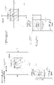
以下、実施例に基づいて本発明を詳細に説明する。図1は、本実施例のパチンコ機GMを示す斜視図である。このパチンコ機GMは、島構造体に着脱可能に装着される矩形枠状の木製外枠1と、外枠1に固着されたヒンジ2を介して開閉可能に枢着される前枠3とで構成されている。この前枠3には、遊技盤5が、裏側からではなく、表側から着脱自在に装着され、その前側には、ガラス扉6と前面板7とが夫々開閉自在に枢着されている。
Hereinafter, the present invention will be described in detail based on examples. FIG. 1 is a perspective view showing the pachinko machine GM of this embodiment. This pachinko machine GM consists of a rectangular frame-shaped wooden
ガラス扉6の外周には、LEDランプなどによる電飾ランプが、略C字状に配置されている。一方、ガラス扉6の上部左右位置と下側には、全3個のスピーカが配置されている。上部に配置された2個のスピーカは、各々、左右チャンネルR,Lの音声を出力し、下側のスピーカは低音を出力するよう構成されている。
Illuminations lamps such as LED lamps are arranged in a substantially C shape on the outer periphery of the
前面板7には、発射用の遊技球を貯留する上皿8が装着され、前枠3の下部には、上皿8から溢れ出し又は抜き取った遊技球を貯留する下皿9と、発射ハンドル10とが設けられている。発射ハンドル10は発射モータと連動しており、発射ハンドル10の回動角度に応じて動作する打撃槌によって遊技球が発射される。
An
上皿8の外周面には、チャンスボタン11が設けられている。このチャンスボタン11は、遊技者の左手で操作できる位置に設けられており、遊技者は、発射ハンドル10から右手を離すことなくチャンスボタン11を操作できる。このチャンスボタン11は、通常時には機能していないが、ゲーム状態がボタンチャンス状態となると内蔵ランプが点灯されて操作可能となる。なお、ボタンチャンス状態は、必要に応じて設けられるゲーム状態である。
A
また、チャンスボタン11の下方には、ロータリースイッチ型の音量スイッチVLSWが配置されており、遊技者が音量スイッチVLSWを操作することで、無音レベル(=0)から最高レベル(=7)まで、スピーカ音量を8段階に調整できるようになっている。なお、スピーカの音量は、係員だけが操作可能な設定スイッチ(不図示)によって初期設定されており、遊技者が音量スイッチVLSWを操作しない限り、初期設定音量が維持される。また、異常事態が発生したことを報知する異常報知音は、係員による初期設定音量や、遊技者の設定音量に拘らず最高音量で放音される。
Further, a rotary switch type volume switch VLSW is arranged below the
上皿8の右部には、カード式球貸し機に対する球貸し操作用の操作パネル12が設けられ、カード残額を3桁の数字で表示する度数表示部と、所定金額分の遊技球の球貸しを指示する球貸しスイッチと、ゲーム終了時にカードの返却を指令する返却スイッチとが設けられている。
On the right side of the
図2に示すように、遊技盤5の表面には、金属製の外レールと内レールとからなるガイドレール13が環状に設けられ、その略中央には、中央開口HOが設けられている。そして、中央開口HOの下方には、不図示の可動演出体が隠蔽状態で収納されており、可動予告演出時には、その可動演出体が上昇して露出状態となることで、所定の信頼度の予告演出を実現している。ここで、予告演出とは、遊技者に有利な大当り状態が招来することを不確定に報知する演出であり、予告演出の信頼度とは、大当り状態が招来する確率を意味している。
As shown in FIG. 2, on the surface of the
中央開口HOには、大型(例えば、横1280×縦1024ピクセル)の液晶カラーディスプレイ(LCD)で構成されたメイン表示装置DS1が配置され、メイン表示装置DS1の右側には、小型(例えば、横480×縦800ピクセル)の液晶カラーディスプレイで構成された可動式のサブ表示装置DS2が配置されている。メイン表示装置DS1は、大当り状態に係わる特定図柄を変動表示すると共に背景画像や各種のキャラクタなどをアニメーション的に表示する装置である。この表示装置DS1は、中央部に特別図柄表示部Da~Dcと右上部に普通図柄表示部19とを有している。そして、特別図柄表示部Da~Dcでは、大当り状態の招来を期待させるリーチ演出が実行されることがあり、特別図柄表示部Da~Dc及びその周りでは、適宜な予告演出などが実行される。
A main display device DS1 composed of a large (for example, 1280 horizontal × 1024 vertical pixels) liquid crystal color display (LCD) is arranged in the central opening HO, and a small size (for example, horizontal) is arranged on the right side of the main display device DS1. A movable sub-display device DS2 composed of a liquid crystal color display (480 × 800 pixels in height) is arranged. The main display device DS1 is a device that displays a specific symbol related to a jackpot state in a variable manner and displays a background image, various characters, and the like in an animation manner. The display device DS1 has a special symbol display unit Da to Dc in the central portion and a normal
サブ表示装置DS2は、通常時には、その表示画面が遊技者に見やすい角度に傾斜した静止状態で画像情報を表示している。但し、所定の予告演出時には、遊技者に見やすい角度に傾斜角度を変えながら、図示の左側に移動する共に、所定の予告画像を表示するようになっている。 Normally, the sub-display device DS2 displays image information in a stationary state in which the display screen is tilted at an angle that is easy for the player to see. However, at the time of the predetermined advance notice effect, the predetermined advance notice image is displayed while moving to the left side of the figure while changing the inclination angle to an angle that is easy for the player to see.
すなわち、実施例のサブ表示装置DS2は、単なる表示装置ではなく、予告演出を実行する可動演出体としても機能している。ここで、サブ表示装置DS2による予告演出は、その信頼度が高く設定されており、遊技者は、大きな期待感をもってサブ表示装置DS2の移動動作に注目することになる。 That is, the sub-display device DS2 of the embodiment is not only a display device but also functions as a movable staging body that executes a warning staging. Here, the notice effect by the sub-display device DS2 is set with high reliability, and the player pays attention to the moving operation of the sub-display device DS2 with great expectation.
ところで、遊技球が落下移動する遊技領域には、第1図柄始動口15a、第2図柄始動口15b、第1大入賞口16a、第2大入賞口16b、普通入賞口17、及び、ゲート18が配設されている。これらの入賞口15~18は、それぞれ内部に検出スイッチを有しており、遊技球の通過を検出できるようになっている。
By the way, in the game area where the game ball falls and moves, the first symbol start opening 15a, the second symbol start opening 15b, the first big winning
第1図柄始動口15aの上部には、導入口INから進入した遊技球がシーソー状又はルーレット状に移動した後に、第1図柄始動口15に入賞可能に構成された演出ステージ14が配置されている。そして、第1図柄始動口15に遊技球が入賞すると、特別図柄表示部Da~Dcの変動動作が開始されるよう構成されている。
At the upper part of the first
第2図柄始動口15bは、左右一対の開閉爪を備えた電動式チューリップで開閉されるように構成され、普通図柄表示部19の変動後の停止図柄が当り図柄を表示した場合には、所定時間だけ、若しくは、所定個数の遊技球を検出するまで、開閉爪が開放されるようになっている。
The second
なお、普通図柄表示部19は、普通図柄を表示するものであり、ゲート18を通過した遊技球が検出されると、普通図柄が所定時間だけ変動し、遊技球のゲート18の通過時点において抽出された抽選用乱数値により決定される停止図柄を表示して停止する。
The normal
第1大入賞口16aは、前後方向に進退するスライド盤を有して構成され、第2大入賞口16bは、下端が軸支されて前方に開放する開閉板を有して構成されている。第1大入賞口16aや第2大入賞口16bの動作は、特に限定されないが、この実施例では、第1大入賞口16aは、第1図柄始動口15aに対応し、第2大入賞口16bは、第1図柄始動口15bに対応するよう構成されている。
The first big winning
すなわち、第1図柄始動口15aに遊技球が入賞すると、特別図柄表示部Da~Dcの変動動作が開始され、その後、所定の大当り図柄が特別図柄表示部Da~Dcに整列すると、第1大当りたる特別遊技が開始され、第1大入賞口16aのスライド盤が、前方に開放されて遊技球の入賞が容易化される。
That is, when the game ball wins in the first symbol start opening 15a, the variable operation of the special symbol display units Da to Dc is started, and then when the predetermined jackpot symbols are aligned with the special symbol display portions Da to Dc, the first jackpot The barrel special game is started, and the slide board of the first large winning
一方、第2図柄始動口15bへの遊技球の入賞によって開始された変動動作の結果、所定の大当り図柄が特別図柄表示部Da~Dcに整列すると、第2大当りたる特別遊技が開始され、第2大入賞口16bの開閉板が開放されて遊技球の入賞が容易化される。特別遊技(大当り状態)の遊技価値は、整列する大当り図柄などに対応して種々相違するが、何れの遊技価値が付与されるかは、遊技球の入賞タイミングに応じた抽選結果に基づいて予め決定される。
On the other hand, as a result of the variable operation started by winning the game ball to the second symbol start opening 15b, when the predetermined jackpot symbols are aligned with the special symbol display units Da to Dc, the second jackpot special game is started and the second jackpot is started. The opening / closing plate of the two major winning
典型的な大当り状態では、大入賞口16の開閉板が開放された後、所定時間が経過し、又は所定数(例えば10個)の遊技球が入賞すると開閉板が閉じる。このような動作は、最大で例えば15回まで継続され、遊技者に有利な状態に制御される。なお、特別図柄表示部Da~Dcの変動後の停止図柄が特別図柄のうちの特定図柄であった場合には、特別遊技の終了後のゲームが高確率状態(確変状態)となるという特典が付与される。
In a typical big hit state, the opening / closing plate closes when a predetermined time elapses after the opening / closing plate of the large winning
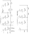
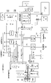
図3は、上記した各動作を実現するパチンコ機GMの全体回路構成を示すブロック図であり、図4(a)はその一部を詳細に図示したものである。 FIG. 3 is a block diagram showing the overall circuit configuration of the pachinko machine GM that realizes each of the above-mentioned operations, and FIG. 4A is a detailed diagram of a part thereof.
図3に示す通り、このパチンコ機GMは、AC24Vを受けて各種の直流電圧や、電源異常信号ABN1、ABN2を出力する電源基板20と、遊技制御動作を中心統括的に担う主制御基板21と、音声演出用の回路素子SNDを搭載した演出インタフェイス基板22と、主制御基板21から受けた制御コマンドCMDに基づいてランプ演出、音声演出、及び画像演出を統一的に実行する演出制御基板23と、演出制御基板23と表示装置DS1,DS2の間に位置する液晶インタフェイス基板24と、主制御基板21から受けた制御コマンドCMD’に基づいて払出モータMを制御して遊技球を払い出す払出制御基板25と、遊技者の操作に応答して遊技球を発射させる発射制御基板26と、を中心に構成されている。
As shown in FIG. 3, this pachinko machine GM has a
本実施例の場合、演出インタフェイス基板22と、演出制御基板23と、液晶インタフェイス基板24とは、配線ケーブルを経由することなく、雄型コネクタと雌型コネクタとを直結されている。そのため、各電子回路の回路構成を複雑高度化しても基板全体の収納空間を最小化できると共に、接続ラインを最短化することで耐ノイズ性を高めることができる。
In the case of this embodiment, the staging
図示の通り、主制御基板21が出力する制御コマンドCMD’は、主基板中継基板33を経由して、払出制御基板25に伝送される。一方、主制御基板21が出力する制御コマンドCMDは、演出インタフェイス基板22を経由して演出制御基板23に伝送される。制御コマンドCMD,CMD’は、何れも16bit長であるが、8bit長毎に2回に分けてパラレル送信される。
As shown in the figure, the control command CMD'output by the
主制御基板21と払出制御基板25には、ワンチップマイコンを含むコンピュータ回路が搭載されている。また、演出制御基板23には、VDP回路(Video Display Processor )52や内蔵CPU回路51などのコンピュータ回路が内蔵された複合チップ50が搭載されている。そこで、これらの制御基板21、25、23と、演出インタフェイス基板22や液晶インタフェイス基板24に搭載された回路、及びその回路によって実現される動作を機能的に総称して、本明細書では、主制御部21、演出制御部23、及び払出制御部25と言うことがある。なお、主制御部21に対して、演出制御部23と、払出制御部25がサブ制御部となる。
A computer circuit including a one-chip microcomputer is mounted on the
また、このパチンコ機GMは、図3の破線で囲む枠側部材GM1と、遊技盤5の背面に固定された盤側部材GM2とに大別されている。枠側部材GM1には、ガラス扉6や前面板7が枢着された前枠3と、その外側の木製外枠1とが含まれており、機種の変更に拘わらず、長期間にわたって遊技ホールに固定的に設置される。一方、盤側部材GM2は、機種変更に対応して交換され、新たな盤側部材GM2が、元の盤側部材の代わりに枠側部材GM1に取り付けられる。なお、枠側部材1を除く全てが、盤側部材GM2である。
Further, the pachinko machine GM is roughly classified into a frame-side member GM1 surrounded by a broken line in FIG. 3 and a board-side member GM2 fixed to the back surface of the
図3の破線枠に示す通り、枠側部材GM1には、電源基板20と、払出制御基板25と、発射制御基板26と、枠中継基板36とが含まれており、これらの回路基板が、前枠3の適所に各々固定されている。一方、遊技盤5の背面には、主制御基板21、演出制御基板23が、表示装置DS1,DS2やその他の回路基板と共に固定されている。そして、枠側部材GM1と盤側部材GM2とは、一箇所に集中配置された接続コネクタC1~C4によって電気的に接続されている。
As shown in the broken line frame of FIG. 3, the frame-
電源基板20は、接続コネクタC2を通して、主基板中継基板33に接続され、接続コネクタC3を通して、電源中継基板34に接続されている。そして、電源基板20には、交流電源の投入と遮断とを監視する電源監視部MNTが設けられている。電源監視部MNTは、交流電源の遮断を検知すると、電源異常信号ABN1,ABN2を、直ちにLレベルに遷移させる。なお、電源異常信号ABN1,ABN2は、電源投入後に速やかにHレベルとなる。
The
主基板中継基板33は、電源基板20から出力される電源異常信号ABN1、バックアップ電源BAK、及びDC5V,DC12V,DC35Vを、そのまま主制御部21に出力している。また、電源中継基板34は、電源基板20から受けた交流及び直流の電源電圧DC5V,DC12V,DC35Vを、そのまま演出インタフェイス基板22に出力している。
The main
図示の通り、演出インタフェイス基板22には、音声プロセッサ27などの音声回路SNDが搭載され、演出制御基板23には、VDP回路52や内蔵CPU回路51などのコンピュータ回路が内蔵された複合チップ50が搭載されている。以下、内蔵CPU回路をCPU回路と略称することがある。
As shown in the figure, the
演出インタフェイス基板22には、電源投入時に、電源電圧の上昇を検知して各種のリセット信号RT3,RT4を生成するリセット回路RST3,RST4が搭載されている。先ず、リセット回路RST3は、電源基板20から配電された直流電圧12Vと5Vに基づいて、リセット信号RT3を生成している。そして、リセット信号RT3は、音声メモリ28だけを電源リセットして、そのまま演出制御基板23に伝送される。
The
演出制御基板23に伝送されたリセット信号RT3は、図4(a)に示す通り、ANDゲートG1において、WDT(Watch Dog Timer )回路58の出力とAND演算され、システムリセット信号SYSとして、CPU回路51やVDP回路52を電源リセットしている(図4(a)及び図4(d)参照)。
As shown in FIG. 4A, the reset signal RT3 transmitted to the
リセット回路RST3が生成するリセット信号RT3は、電源投入後、電源リセット信号として所定時間Lレベルを維持した後、Hレベルに上昇する。しかし、その後、直流電圧12V又は直流電圧5Vの何れか一以上が降下した場合(通常は電源遮断時)には、リセット信号RT3のレベル降下に対応して、システムリセット信号SYSもLレベルに降下するので、演出制御基板23のCPU回路51とVDP回路52は動作停止状態となる。
The reset signal RT3 generated by the reset circuit RST3 rises to the H level after maintaining the L level as the power reset signal for a predetermined time after the power is turned on. However, after that, when any one or more of the
このシステムリセット信号SYSは、WDT回路58の出力(正常時にはHレベル)に基づいても変化するので、リセット信号RT3=Hの状態で、プログラム暴走時などに起因して、WDT回路58の出力がLレベルに降下することに対応して、システムリセット信号SYSもLレベルに変化して、CPU回路51やVDP回路52を異常リセットする(図4(d)参照)。
Since this system reset signal SYS also changes based on the output of the WDT circuit 58 (H level at normal times), the output of the
一方、リセット回路RST4は、電源基板20から配電された5Vを降下して生成された3.3Vに基づいて、リセット信号RT4を生成している。このリセット信号RT4は、電源投入時の電源リセット信号として、音声プロセッサ27を電源リセットしている。
On the other hand, the reset circuit RST4 generates a reset signal RT4 based on 3.3V generated by dropping 5V distributed from the
図示の通り、リセット回路RST4には、演出制御基板23から返送されたシステムリセット信号SYSも供給されているので、CPU回路51やVDP回路52の異常リセット時には、これらの回路の異常リセットに同期して、音声プロセッサ27も異常リセットされる。この結果、音声演出は、画像演出やランプ演出と共に初期状態に戻ることになり、不自然な音声演出が継続するおそれがない。
As shown in the figure, the reset circuit RST4 is also supplied with the system reset signal SYS returned from the
次に、枠側部材GM1たる払出制御基板25は、中継基板を介することなく、電源基板20に直結されて、主制御部21が受けると同様の電源異常信号ABN2や、バックアップ電源BAKを、その他の電源電圧と共に受けている。また、主制御部21と払出制御部25には、各々、リセット回路RST1,RST2が搭載されており、電源投入時に電源リセット信号が生成され、各コンピュータ回路が電源リセットされるよう構成されている。
Next, the
このように、本実施例では、主制御部21と、払出制御部25と、演出インタフェイス基板22に、各々、リセット回路RST1~RST4を配置しており、システムリセット信号SYSが回路基板間で伝送されることがない。すなわち、システムリセット信号SYSを伝送する配線ケーブルが存在しないので、配線ケーブルに重畳するノイズによって、コンピュータ回路が異常リセットされるおそれが解消される。
As described above, in this embodiment, the reset circuits RST1 to RST4 are arranged on the
但し、主制御部21や払出制御部25に設けられたリセット回路RST1,RST2は、各々ウォッチドッグタイマを内蔵しており、各制御部21,25のCPUから、定時的なクリアパルスを受けない場合には、各CPUは強制的にリセットされる。
However, the reset circuits RST1 and RST2 provided in the
また、主制御部21には、係員が操作可能な初期化スイッチSWが配置されており、電源投入時、初期化スイッチSWがON操作されたか否かを示すRAMクリア信号CLRが出力されるよう構成されている。このRAMクリア信号CLRは、主制御部21と払出制御部25のワンチップマイコンに伝送され、各制御部21,25のワンチップマイコンの内蔵RAMの全領域を初期設定するか否かを決定している。
Further, an initialization switch SW that can be operated by a staff member is arranged in the
また、主制御部21及び払出制御部25は、電源基板20から電源異常信号ABN1,ABN2を受けることによって、停電や営業終了に先立って、必要な終了処理を開始するようになっている。また、バックアップ電源BAKは、営業終了や停電により交流電源24Vが遮断された後も、主制御部21と払出制御部25のワンチップマイコンの内蔵RAMのデータを保持するDC5Vの直流電源である。したがって、主制御部21と払出制御部25は、電源遮断前の遊技動作を電源投入後に再開できることになる(電源バックアップ機能)。このパチンコ機では少なくとも数日は、各ワンチップマイコンのRAMの記憶内容が保持されるよう設計されている。
Further, the
図3に示す通り、主制御部21は、払出制御部25から、遊技球の払出動作を示す賞球計数信号や、払出動作の異常に係わるステイタス信号CONや、動作開始信号BGNを受信している。ステイタス信号CONには、例えば、補給切れ信号、払出不足エラー信号、下皿満杯信号が含まれる。動作開始信号BGNは、電源投入後、払出制御部25の初期動作が完了したことを主制御部21に通知する信号である。
As shown in FIG. 3, the
また、主制御部21は、遊技盤中継基板32を経由して、遊技盤5の各遊技部品に接続されている。そして、遊技盤上の各入賞口16~18に内蔵された検出スイッチのスイッチ信号を受ける一方、電動式チューリップなどのソレノイド類を駆動している。ソレノイド類や検出スイッチは、主制御部21から配電された電源電圧VB(12V)で動作するよう構成されている。また、図柄始動口15への入賞状態などを示す各スイッチ信号は、電源電圧VB(12V)と電源電圧Vcc(5V)とで動作するインタフェイスICで、TTLレベル又はCMOSレベルのスイッチ信号に変換された上で、主制御部21に伝送される。
Further, the
先に説明した通り、演出インタフェイス基板22と演出制御基板23と液晶インタフェイス基板24とはコネクタ連結によって一体化されており、演出インタフェイス基板22は、電源中継基板34を経由して、電源基板20から各レベルの直流電圧(5V,12V,35V)を受けている(図3及び図4(a)参照)。直流電圧12Vは、デジタルアンプ29の電源電圧であると共に、LEDランプなどの駆動電圧として使用される。また、直流電圧35Vは、モータの駆動電圧として使用される。
As described above, the
一方、直流電圧5Vは、演出インタフェイス基板22各所の回路素子の電源電圧として供給されると共に、2つのDC/DCコンバータDC1,DC2に供給されて3.3Vと1.0Vが生成される(図4(a)参照)。生成された直流電圧3.3Vと1.0Vは、各々、I/O(入出力)用と、チップコア用の電源電圧として音声プロセッサ27に供給される。また、直流電圧3.3Vは、リセット回路RST4が生成する電源リセット信号RT4の基礎電圧となる。
On the other hand, the DC voltage of 5V is supplied as the power supply voltage of the circuit elements of the
演出インタフェイス基板22に配電された直流電圧5Vは、DC/DCコンバータDC1で生成された3.3Vと共に、演出制御基板23に配電される。そして、演出制御基板23に配電された直流電圧3.3Vは、電源電圧として、複合チップ50や、PROM53及びCGROM55に供給される。
The
図4(a)に示す通り、演出制御基板23には、2つのDC/DCコンバータDC3,DC4が配置されており、各々に供給される直流電圧5Vに基づいて、1.5Vと1.05Vを生成している。ここで、直流電圧1.05Vは、複合チップ50のチップコア用の電源電圧であり、直流電圧1.5Vは、DRAM54とのI/O(入出力)用の電源電圧である。したがって、直流電圧1.5Vは、電源電圧として、DRAM54にも供給される。
As shown in FIG. 4A, two DC / DC converters DC3 and DC4 are arranged on the
図3に示す通り、演出インタフェイス基板22は、主制御部21から制御コマンドCMDとストローブ信号STBとを受けて、演出制御基板23に転送している。より詳細には、図4(a)に示す通りであり、制御コマンドCMDとストローブ信号STBは、入力バッファ40を経由して、演出制御基板23の複合チップ50(CPU回路51)に転送される。ここで、ストローブ信号STBは、受信割込み信号IRQ_CMD であり、演出制御CPU63は、受信割込み信号IRQ_CMD を受けて起動される割込み処理プログラム(割込みハンドラ)に基づいて、制御コマンドCMDを取得している。
As shown in FIG. 3, the staging
図4(a)に示す通り、演出インタフェイス基板22の入力バッファ44は、枠中継基板35,36からチャンスボタン11や音量スイッチVLSWのスイッチ信号を受け、各スイッチ信号を演出制御基板23のCPU回路51に伝送している。具体的には、音量スイッチVLSWの接点位置(0~7)を示すエンコーダ出力の3bit長と、チャンスボタン11のON/OFF状態を示す1bit長をCPU回路51に伝送している。
As shown in FIG. 4A, the
また、演出インタフェイス基板22には、ランプ駆動基板30やモータランプ駆動基板31が接続されると共に、枠中継基板35,36を経由して、ランプ駆動基板37にも接続されている。図示の通り、ランプ駆動基板30に対応して、出力バッファ42が配置され、モータランプ駆動基板31に対応して、入力バッファ43aと出力バッファ43bが配置されている。なお、図4(a)では、便宜上、入力バッファ43aと出力バッファ43bを総称して、入出力バッファ43と記載している。入力バッファ43aは、可動演出体たる役物の現在位置(演出モータM1~Mnの回転位置)を把握する原点センサの出力SN0~SNnを受けて、演出制御基板23のCPU回路51に伝送している。
Further, the
ランプ駆動基板30、モータランプ駆動基板31、及び、ランプ駆動基板37には、同種のドライバICが搭載されており、演出インタフェイス基板22は、演出制御基板23から受けるシリアル信号を、各ドライバICに転送している。シリアル信号は、具体的には、ランプ(モータ)駆動信号SDATAとクロック信号CKであり、駆動信号SDATAがクロック同期方式で各ドライバICに伝送され、多数のLEDランプや電飾ランプによるランプ演出や、演出モータM1~Mnによる役物演出が実行される。
The same type of driver IC is mounted on the
本実施例の場合、ランプ演出は、三系統のランプ群CH0~CH2によって実行されており、ランプ駆動基板37は、枠中継基板35,36を経由して、CH0のランプ駆動信号SDATA0を、クロック信号CK0に同期して受けている。なお、シリアル信号として伝送される一連のランプ駆動信号SDATA0は、動作制御信号ENABLE0がアクティブレベルに変化したタイミングで、ドライバICからランプ群CH0に出力されることで一斉に点灯状態が更新される。
In the case of this embodiment, the lamp effect is executed by the lamp groups CH0 to CH2 of the three systems, and the
以上の点は、ランプ駆動基板30についても同様であり、ランプ駆動基板30のドライバICは、ランプ群CH1のランプ駆動信号SDATA1を、クロック信号CK1に同期して受け、動作制御信号ENABLE1がアクティブレベルに変化したタイミングで、ランプ群CH1の点灯状態を一斉に更新している。
The above points are the same for the
一方、モータランプ駆動基板31に搭載されたドライバICは、クロック同期式で伝送されるランプ駆動信号を受けてランプ群CH2を駆動すると共に、クロック同期式で伝送されるモータ駆動信号を受けて、複数のステッピングモータで構成された演出モータ群M1~Mnを駆動している。なお、ランプ駆動信号とモータ駆動信号は、一連のシリアル信号SDATA2であって、クロック信号CK1に同期してシリアル伝送され、これを受けたドライバICは、動作制御信号ENABLE2がアクティブレベルに変化するタイミングで、ランプ群CH2やモータ群M1~Mnの駆動状態を更新する。
On the other hand, the driver IC mounted on the motor
続いて、音声回路SNDについて説明する。図4(a)に示す通り、演出インタフェイス基板22には、演出制御基板23のCPU回路51(演出制御CPU63)から受ける指示に基づいて音声信号を再生する音声プロセッサ(音声合成回路)27と、再生される音声信号の元データである圧縮音声データなどを記憶する音声メモリ28と、音声プロセッサ27から出力される音声信号を受けるデジタルアンプ29と、が搭載されている。
Subsequently, the voice circuit SND will be described. As shown in FIG. 4A, the
音声プロセッサ27は、内部回路の異常動作時に、内部回路の設定値を自動的にデフォルト値(初期値)にリセットするWDT回路と、音声制御レジスタSRGとを内蔵して構成されている。そして、音声プロセッサ27は、演出制御CPU63から音声制御レジスタSRGに受ける動作パラメータ(音声コマンドによる設定値)に基づいて、音声メモリ28をアクセスして、必要な音声信号を再生して出力している。
The
図4(a)に示す通り、音声プロセッサ27と、音声メモリ28とは、26bit長の音声アドレスバスと、16bit長の音声データバスで接続されている。そのため、音声メモリ28には、1Gbit(=226*16)のデータが記憶可能となる。
As shown in FIG. 4A, the
音声制御レジスタSRGは、レジスタバンク1~レジスタバンク6に区分され、各々、00H~FFHのレジスタ番号で特定される。したがって、所定の設定動作は、レジスタバンクを特定した上で、演出制御CPU63が、所定のレジスタ番号(1バイト長)の音声制御レジスタSRGに、1バイト長の動作パラメータを書込むことで実現される。
The voice control register SRG is divided into
本実施例の場合、音声制御レジスタSRGのレジスタ番号(00H~FFH)は、演出制御CPU63のアドレス空間CS3に対応しており、例えば、レジスタ番号XXHの音声制御レジスタSRGに、動作パラメータYYHを設定する場合には、演出制御CPU63は、アドレス空間CS3のゼロ番地にXXHを書込み、次に、1番地にYYHを書込むことになる。すなわち、演出制御CPU63は、そのデータバスにXXHとYYHを、この順番に書き出すことになる。なお、本明細書において、添え字Hや、0X/0xの接頭記号は、数値が16進数表示であることを示している。
In the case of this embodiment, the register numbers (00H to FFH) of the voice control register SRG correspond to the address space CS3 of the
また、本明細書において、アドレス空間CS0~CS7とは、揮発性の有無を含むメモリ種別や、データバス幅(8/16/32ビット)を、各々、規定可能なCPU回路51にとって外部メモリを意味する(内蔵メモリを除く)。このアドレス空間CS0~CS7は、異なるチップセレクト信号CS0~CS7で選択され、READ/WRITE アクセス時に機能するREAD/WRITE 制御信号がメモリ種別に対応して最適化できるよう設定可能に構成されている。なお、この設定動作は、バスステートコントローラ66に対して実行される。
Further, in the present specification, the address spaces CS0 to CS7 refer to the external memory for the
図4(e)は、演出制御CPU63による音声レジスタSRGへの設定動作を図示したものであり、2bit長のアドレスバスA1-A0と、1バイト長のデータバスD7-D0の内容が示されている。なお、本実施例では、チップセレクト信号CS3は、アドレス空間CS3をアクセスする場合に、自動的にアクティブになるよう、電源投入時に設定されるが、この点は図6や図12に関して後述する。
FIG. 4E illustrates the setting operation of the sound register SRG by the
何れにしても、本実施例の場合、音声メモリ28に記憶された圧縮音声データは、13bit長のフレーズ番号NUM(000H~1FFFH)で特定されるフレーズ(phrase)圧縮データであり、一連の背景音楽の一曲分(BGM)や、ひと纏まりの演出音(予告音)などが、最高8192種類(=213)、各々、フレーズ番号NUMに対応して記憶されている。そして、このフレーズ番号NUMは、演出制御CPU63から音声プロセッサ27の音声制御レジスタSRGに伝送される音声コマンドの設定値(動作パラメータ)によって特定される。
In any case, in the case of this embodiment, the compressed voice data stored in the
前記の通り、上記の構成を有する音声メモリ28は、リセット信号RT3で電源リセットされ、音声プロセッサ27は、リセット信号RT4で電源リセットされる。図4(c)に示す通り、リセット信号RT4は、電源投入後、所定のアサート期間ASRT(Lレベル区間)を経て、Hレベルに立ち上がるが、本実施例では、その後、音声プロセッサ27の内部回路が自動的に機能して、初期化シーケンス処理が実行されるよう構成されている。なお、この初期化シーケンス処理は、所定の手順で実行される内部動作であり、初期化シーケンス処理の動作中は、演出制御CPU63が音声レジスタSRGをアクセスすることはできない。
As described above, the
そして、内部動作たる初期化シーケンス処理が完了すると、CPU回路51に対する割込み信号IRQ_SND がLレベルに変化し、CPU回路51(演出制御CPU63)は、割込み信号IRQ_SND に基づき割込み処理プログラムを実行する。そして、所定の命令に基づいて割込み信号IRQ_SND がHレベルに戻されるが、その詳細については、図14(c)を参照して更に後述する。
Then, when the initialization sequence processing, which is an internal operation, is completed, the interrupt signal IRQ_SND for the
図4(a)に示す通り、演出制御部23のCPU回路51のデータバスとアドレスバスは、液晶インタフェイス基板24に搭載された時計回路(real time clock )38と演出データメモリ39にも及んでいる。時計回路38は、CPU回路51のアドレスバスの下位4bitと、データバスの下位4bitに接続されており、チップセレクト信号CS4で時計回路38が選択された状態では、CPU回路51が、(4bit長アドレス値を有する)内部レジスタを任意にアクセスできるよう構成されている。
As shown in FIG. 4A, the data bus and address bus of the
また、演出データメモリ39は、高速アクセス可能なメモリ素子SRAM(Static Random Access Memory )であって、CPU回路51のアドレスバスの16bitと、データバスの下位16bitに接続されており、チップセレクト信号CS4でチップ選択された状態では、SRAM(演出データメモリ)39に記憶されている遊技実績情報その他が、CPU回路51から適宜にR/Wアクセスされるようになっている。なお、チップセレクト信号CS4で選択されるアドレス空間CS4において、0番地から15番地までは時計回路38に付番されているので、SRAM39では使用しない。
Further, the
時計回路38と演出データメモリ39は、不図示の二次電池で駆動されており、この二次電池は、遊技動作中、電源基板20からの給電電圧によって適宜に充電される。そのため、電源遮断後も、時計回路38の計時動作が継続され、また、演出データメモリ39に記憶された遊技実績情報が、永続的に記憶保持されることになる(不揮発性を付与)。なお、時計回路(RTC)38は、CPU回路51に対して、割込み信号IRQ_RTC を出力可能に構成されている(RTC割込み)。このRTC割込みには、日、曜日、時、分、秒が特定可能なアラーム割込みと、所定時間経過後に起動されるタイマ割込みが存在するが、本実施例では、毎日の営業終了時に、日々の遊技実績情報を更新するアラーム割込みを活用している。
The
図4(a)の右側に示す通り、演出制御基板23には、CPU回路51やVDP回路52を内蔵する複合チップ50と、CPU回路51の制御プログラムを記憶する制御メモリ(PROM)53と、大量のデータを高速にアクセス可能なDRAM(Dynamic Random Access Memory)54と、演出制御に必要な大量のCGデータを記憶するCGROM55と、が搭載されている。
As shown on the right side of FIG. 4A, the
図7に関して後述するように、制御メモリ(PROM)53は、本実施例では、チップセレクト信号CS0で選択されるアドレス空間CS0に位置付けされている。また、DDR(Double-Data-Rate 3)で構成されるDRAM(Dynamic Random Access Memory)54は、チップセレクト信号CS5で選択されるアドレス空間CS5に位置付けされている。 As will be described later with respect to FIG. 7, the control memory (PROM) 53 is positioned in the address space CS0 selected by the chip select signal CS0 in this embodiment. Further, the DRAM (Dynamic Random Access Memory) 54 composed of DDR (Double-Data-Rate 3) is positioned in the address space CS5 selected by the chip select signal CS5.
図5(a)は、演出制御部23を構成する複合チップ50について、関連する回路素子も含めて図示した回路ブロック図である。図示の通り、実施例の複合チップ50には、所定時間毎にディスプレイリストDLを発行するCPU回路51と、発行されたディスプレイリストDLに基づいて画像データを生成して表示装置DS1,DS2を駆動するVDP回路52とが内蔵されている。そして、CPU回路51とVDP回路52とは、互いの送受信データを中継するCPUIF回路56を通して接続されている。
FIG. 5A is a circuit block diagram showing the
なお、VDP回路52には、音声プロセッサ27と同等の機能を発揮する音声回路SNDが内蔵されているが、これから説明する最初の実施例では、音声回路SNDを活用していない。但し、最後に説明する実施例のように、VDP回路52に内蔵された音声回路SNDを活用すれば、音声メモリ28や音声プロセッサ27の配置が不要となる。
The
先ず、CPU回路51は、発振器OSC1の発振出力(例えば100/3MHz)をHCLKI 端子に受けて、これを周波数逓倍(例えば8逓倍)して、266.7MHz程度のCPU動作クロックとしている。ここで、発振器OSC1は、スペクトラムス拡散波を出力するよう構成されることで、電波障害/電磁妨害を防止するEMI(Electromagnetic Interference)対策を図っている。
First, the
一方、VDP回路52は、発振器OSC2の発振出力(例えば40MHz)をPLLREF端子に受け、PLL(Phase Locked Loop )回路で、適宜に周波数逓倍した上で、VDP回路52のシステムクロック、表示装置用の表示クロック(ドットクロックなど)、及び、外付けDRAM54のDDRクロックとして使用している。すなわち、発振器OSC2の出力は、VDP回路52全体のリファレンスクロックとして機能している。なお、PLL回路の周波数逓倍比は、所定の設定端子への設定値で規定される。
On the other hand, the
そこで、このリファレンスクロックの重要性を考慮して、本実施例では、発振器OSC2をVDP回路52と同じ電源電圧3.3Vで動作させると共に、出力イネーブル端子OEがHレベル(=3.3V)であることを条件に、リファレンスクロックを発振出力するよう構成されている。そして、万一、電源電圧3.3Vが所定レベル以下に低下した場合には、その後、正常な演出動作は望めないので、マスク不能の割込み(NMI)が生じるよう構成されている。
Therefore, in consideration of the importance of this reference clock, in this embodiment, the oscillator OSC2 is operated at the same power supply voltage of 3.3V as the
また、複合チップ50には、HBTSL 端子が設けられ、HBTSL 端子の論理レベルに基づいて、電源投入(CPUリセット)後に実行されるブートプログラム(初期設定プログラム)が、CGROM55に記憶されているか(HBTSL =H)、それ以外のメモリに記憶されているか(HBTSL =L)を特定している。図示の通り、この実施例では、HBTSL =Lレベルに設定されており、演出制御CPU63のアドレス空間CS0のゼロ番地が、CGROM以外に割り当てられ、具体的には、アドレス空間CS0は、制御メモリ53に割り当てられている。
Further, the
一方、HBTSL 端子=Hレベルに設定されている場合(破線参照)は、演出制御CPU63のアドレス空間CS0のゼロ番地が、CGROM55に割り当てられる。この場合は、CGROM55のメモリ種別と、バス幅(64/32/16bit)とが、2bit長のHBTBWD端子と、4bit長のHBTRMSL 端子への入力値に基づいて各々特定されようになっている。なお、これらの点は、図34に基づいて更に後述する。
On the other hand, when the HBTSL terminal = H level is set (see the broken line), the zero address of the address space CS0 of the
続いて、CPU回路51とVDP回路52について、互いの送受信データを中継するCPUIF回路56について説明する。図5(a)に示す通り、CPUIF回路56には、制御プログラムや必要な制御データを不揮発的に記憶する制御メモリ(PROM)53と、2Mバイト程度の記憶容量を有するワークメモリ(RAM)57とが接続され、各々、CPU回路51からアクセス可能に構成されている。先に説明した通り、制御メモリ(PROM)53は、チップセレクト信号CS0で選択されるアドレス空間CS0に位置付けられ、ワークメモリ(RAM)57は、チップセレクト信号CS6で選択されるアドレス空間CS6に位置付けられている。
Subsequently, the CPU IF
このワークメモリ(RAM)57には、表示装置DS1,DS2の各一フレームを特定する一連の指示コマンドが記載されたディスプレイリストDLを、一次的に記憶するDLバッファBUFが確保されている。本実施例の場合、一連の指示コマンドには、CGROM55から画像素材(テクスチャ)を読み出してデコード(展開)するためのTXLOADコマンドなどのテクスチャロード系コマンドと、デコード(展開)先のVRAM領域(インデックス空間)を予め特定するなどの機能を有するSETINDEXコマンドなどのテクスチャ設定系コマンドと、デコード(展開)後の画像素材を仮想描画空間の所定位置に配置するためのSPRITEコマンドなどのプリミティブ描画系コマンドと、描画系コマンドによって仮想描画空間に描画された画像のうち、実際に表示装置に描画する描画領域を特定するためのSETDAVR コマンドやSETDAVF コマンドなどの環境設定コマンドと、インデックス空間を管理するインデックステーブルIDXTBLに関するインデックステーブル制御系コマンド(WRIDXTBL)が含まれる。 In the work memory (RAM) 57, a DL buffer BUF for temporarily storing a display list DL in which a series of instruction commands for specifying each frame of the display devices DS1 and DS2 are described is secured. In the case of this embodiment, a series of instruction commands include a texture load command such as a TXLOAD command for reading an image material (texture) from the CGROM 55 and decoding (expanding) it, and a VRAM area (index) of the decoding (expanding) destination. Texture setting commands such as the SET INDEX command, which have functions such as specifying the space in advance, and primitive drawing commands such as the SPRITE command for arranging the decoded (expanded) image material at a predetermined position in the virtual drawing space. Of the images drawn in the virtual drawing space by drawing commands, environment setting commands such as the SETDAVR command and SETDAVF command for specifying the drawing area actually drawn on the display device, and the index table IDXTBL that manages the index space. Contains index table control commands (WRIDXTBL) for.
なお、図9(c)には、仮想描画空間(水平X方向±8192:垂直Y方向±8192)と、仮想描画空間の中で任意に設定可能な描画領域と、表示装置DS1,DS2に出力する画像データを一次保存するフレームバッファFBa,FBbにおける実描画領域と、の関係が図示されている。 Note that FIG. 9C shows a virtual drawing space (horizontal X direction ± 8192: vertical Y direction ± 8192), a drawing area that can be arbitrarily set in the virtual drawing space, and outputs to the display devices DS1 and DS2. The relationship with the actual drawing area in the frame buffers FBa and FBb for primary storage of the image data to be performed is illustrated.
次に、CPU回路51は、汎用のワンチップマイコンと同等の性能を有する回路であり、制御メモリ53の制御プログラムに基づき画像演出を統括的に制御する演出制御CPU63と、プログラムが暴走状態になるとCPUを強制リセットするウォッチドッグタイマ(WDT)と、16kバイト程度の記憶容量を有してCPUの作業領域として使用される内蔵RAM59と、CPU63を経由しないでデータ転送を実現するDMAC(Direct Memory Access Controller )60と、複数の入力ポートSi及び出力ポートSoを有するシリアル入出力ポート(SIO)61と、複数の入力ポートPi及び出力ポートPoを有するパラレル入出力ポート(PIO)62と、前記各部の動作を制御するべく設定値が設定される動作制御レジスタREGなどを有して構成されている。但し、外付けのWDT回路58を設けた本実施例では、CPU回路51に内蔵されたウォッチドッグタイマ(WDT)を活用していない。
Next, the
なお、本明細書では、便宜上、入出力ポートとの表現を使用するが、演出制御部23において、入出力ポートには、独立して動作する入力ポートと出力ポートとが含まれている。この点は、以下に説明する入出力回路64pや入出力回路64sについても同様である。
In this specification, the term “input / output port” is used for convenience, but in the
パラレル入出力ポート62は、入出力回路64pを通して外部機器(演出インタフェイス基板22)に接続されており、演出制御CPU63は、入力回路64pを経由して、音量スイッチVLSWのエンコーダ出力3bitと、チャンスボタン11のスイッチ信号と、制御コマンドCMDと、割込み信号STBと、を受信するようになっている。エンコーダ出力3bitと、スイッチ信号1bitは、入出力回路64pを経由して、パラレル入出力ポート(PIO)62に供給されている。
The parallel input /
同様に、受信した制御コマンドCMDは、入出力回路64pを経由して、パラレル入出力ポート(PIO)62に供給されている。また、ストローブ信号STBは、入出力回路64pを経由して、演出制御CPU63の割込み端子に供給されることで、受信割込み処理を起動させている。したがって、受信割込み処理に基づいて、制御コマンドCMDを把握した演出制御CPU63は、演出抽選などを経て、この制御コマンドCMDに対応する音声演出、ランプ演出、モータ演出、及び画像演出を統一的に制御することになる。
Similarly, the received control command CMD is supplied to the parallel input / output port (PIO) 62 via the input /
特に限定されないが、本実施例では、ランプ演出とモータ演出のために、VDP回路52のSMC部(Serial Management Controller)78を使用している。SMC部78は、LEDコントローラとMotorコントローラと、を内蔵した複合コントコントローラであり、クロック同期方式でシリアル信号を出力できるよう構成されている。また、Motorコントローラは、所定の制御レジスタ70への設定値に基づき、任意のタイミングでラッチパルスを出力可能に構成され、また、クロック同期方式でシリアル信号を入力可能に構成されている。
Although not particularly limited, in this embodiment, the SMC unit (Serial Management Controller) 78 of the
そこで、本実施例では、クロック信号に同期してモータ駆動信号やLED駆動信号を、SMC部78から出力させる一方、適宜なタイミングで、ラッチパルスを、動作制御信号ENABLEとして出力するようにしている。また、演出モータ群M1~Mnからの原点センサ信号SN0~SNnをクロック同期方式でシリアル入力するよう構成されている。
Therefore, in this embodiment, the motor drive signal and the LED drive signal are output from the
図4(a)に関して説明した通り、クロック信号CK0~CK2、駆動信号SDATA0~SDATA2、及び、動作制御信号ENABLE0~ENABLE2は、出力バッファ41~43を経由して、所定の駆動基板30,31,37に伝送される。また、原点センサ信号SN0~SNnは、モータランプ駆動基板31から入出力バッファ43を経由して、SMC部78にシリアル入力される。
As described with respect to FIG. 4A, the clock signals CK0 to CK2, the drive signals SDAT0 to SDATA2, and the operation control signals ENABLE0 to ENABLE2 pass through the output buffers 41 to 43, and the
但し、本実施例において、SMC部78を使用することは必須ではない。すなわち、CPU回路51には、汎用のシリアル入出力ポートSIO61が内蔵されているので、これらを使用して、ランプ演出とモータ演出を実行することもできる。
However, it is not essential to use the
具体的には、図5(a)の破線に示す通りであり、破線で示す構成では、シリアル入出力ポートSIO61に内部接続されている入出力回路64sを経由して、クロック信号CK0~CK2、駆動信号SDATA0~SDATA2が出力され、入出力回路64pを経由して動作制御信号ENABLE0~ENABLE2が出力される。なお、便宜上、入出力ポートや入出力回路と表現するが、実際に機能するのは、出力ポートや出力回路である。
Specifically, it is as shown by the broken line in FIG. 5A, and in the configuration shown by the broken line, the clock signals CK0 to CK2, via the input /
ここで、シリアル出力ポートSOは、16段のFIFOレジスタを内蔵して構成されている。そして、DMAC回路60は、演出制御CPU63から動作開始指示(図17(b)ST18参照)を受けて起動し、ランプ/モータ駆動テーブル(図17(b)参照)から、必要な駆動テータを順番に読み出し、シリアル出力ポートSOのFIFOレジスタにDMA転送するよう構成されている。FIFOレジスタに蓄積された駆動データは、クロック同期方式でシリアル出力ポートSOからシリアル出力される。なお、DMAC回路には、複数(例えば7)のDMAチャネルが存在するが、優先度に劣る第3のDMAチャネルでランプ駆動データをDMA転送し、最優先度の第1のDMAチャネルでモータ駆動データをDMA転送するよう構成されている。
Here, the serial output port SO is configured to have a built-in 16-stage FIFO register. Then, the
CPU回路51に内蔵された動作制御レジスタREGは、レジス番号(アドレス値)が0xFF400000以降に付番された8bit、16bit、又は32bit長のレジスタであり、演出制御CPU63から適宜にWRITE/READアクセス可能に構成されている(図7参照)。そのためノイズなどの影響で、動作制御レジスタREGに、不合理な値に設定される可能性がある。
The operation control register REG built in the
但し、例えば、意図的に無限ループ処理を実行させて外付けのWDT回路58を起動させることで、複合チップ50を異常リセットすることができる。この場合、動作制御レジスタREGの値が、電源投入後と同じデフォルト値(初期値)に戻され、且つ、VDP回路52についても、VDPレジスタRGijの値が、デフォルト値(初期値)に戻されることで異常状態が解消される。
However, for example, the
図4(b)は、このリセット動作に関連する回路構成であって、本実施例に特徴的なリセット機構を説明する図面である。なお、本明細書において、RGijと表記するVDPレジスタは、CPU回路51に内蔵された動作制御レジスタREGではなく、VDP回路52の内部動作を制御する制御レジスタ群70(図7参照)の何れかを意味する。また、図4(b)に示すシステム制御回路520とは、VDPレジスタRGij(図7の制御レジスタ群70の何れか)への設定値に基づいて機能するVDP回路52の内部制御回路を意味する(図4(a)参照)。なお、VDPレジスタRGijは、演出制御CPU63のアドレスマップにおいて、チップセレクト信号CS7で選択されるアドレス空間CS7に位置付けられる。
FIG. 4B is a circuit configuration related to this reset operation, and is a drawing illustrating a reset mechanism characteristic of the present embodiment. In the present specification, the VDP register referred to as RGij is not the operation control register REG built in the
以上を踏まえてリセット機構について説明すると、図4(b)に示す通り、複合チップ50は、論理反転されたシステムリセット信号SYSバーを受ける3個のORゲートG2~G4を経由して、内部回路がリセット可能に構成されている。但し、本実施例では、破線で示すように、内蔵WDTを有効化しないので、ORゲートG2の入端子と出力端子は、直結状態となる。
Explaining the reset mechanism based on the above, as shown in FIG. 4B, the
何れにしても、CPU回路51とVDP回路52の間に、パターンチェック回路CHKが設けられ、パターンチェック回路CHKは、パラレル入出力ポート(PIO)62から、所定のキーワード列(リセット用の暗号列)を受けることを条件に、リセット信号RSTを出力するよう構成されている。
In any case, a pattern check circuit CHK is provided between the
そして、複合チップ50の内部回路は、(1)CPU回路51と、(2)VDP回路52の表示回路74と、(3)VDP回路52における表示回路以外とに三分されて、各々、ORゲートG2~G4から第1リセット経路~第3リセット経路のリセット信号を受けるよう構成されている。
The internal circuit of the
先ず、入出力端子が直結状態のORゲートG2は、第1リセット経路に関連しており、システムリセット信号SYSバーに基づき、CPU回路51の全体をシステムリセットされるように構成されている。また、ORゲートG3は、第2リセット経路に関連しており、システムリセット信号SYSバーと、パターンチェック回路CHKからのリセット信号RSTとを受けて、OR論理に基づき、VDP回路52全体をリセット可能に構成されている。
First, the OR gate G2 in which the input / output terminals are directly connected is related to the first reset path, and is configured to system reset the
この第2リセット経路は、電源投入時の電源リセット動作だけでなく、所定の異常を検出した演出制御CPU63が、VDP回路52の全体を異常リセットして初期状態に戻す用途で使用される。具体的には、VDP回路52の内部動作を示す所定のステイタスレジスタRGijに基づき、重大な異常が発生していると判断される場合には、パターンチェック回路CHKからリセット信号RSTを発生させることで、VDP回路52の全体を異常リセットしている。なお、表示回路74は、ORゲートG4を経由して、第2リセット経路→第3リセット経路で異常リセットされる。
This second reset path is used not only for the power reset operation when the power is turned on, but also for the
一方、VDP回路52に内蔵された内部回路は、第4リセット経路で、必要時に個々的にリセットすることも可能に構成されている。個々的にリセット可能な内部回路には、図5(a)に示すインデックステーブルIDXTBL、データ転送回路72、プリローダ73、表示回路74、描画回路76、SMC回路78、及び、音声回路SNDや、図10に示すICM回路が含まれている。
On the other hand, the internal circuit built in the
個別的なリセット動作を実現する手法は、図4(b)の下部に記載の通りであり、例えば、表示回路74は、所定のVDPレジスタRGij(システムコマンドレジスタ)に、第1リセット値を書き込むことで、第4リセット経路4A→第3リセット経路を経てリセットされる。
The method for realizing the individual reset operation is as described in the lower part of FIG. 4 (b). For example, the
また、VDP回路52の各内部回路(72,73,74,76,SND,・・・)は、(1)第1のVDPレジスタRGij(リセットRQレジスタ)に、対象回路を特定する設定値を書き込んだ後、(2)所定のVDPレジスタRGij(システムコマンドレジスタ)に、第2リセット値を書き込むことで、個々的にリセットされる(第4リセット経路4B)。なお、この実施例では使用しないが、音声回路SNDは、第4リセット経路4Bによるリセットだけでなく、所定のVDPレジスタ(回路設定コマンドレジスタ)に、リセット値を書き込むことでもリセット可能である(第4リセット経路4C)。
Further, each internal circuit (72, 73, 74, 76, SND, ...) Of the
本実施例は、上記の構成を有するので、電源投入時やプログラム暴走時に、VDP回路52全体が自動的に初期状態に戻るだけでなく、必要に応じて、各部を初期状態に戻して異常事態の回復を図ることができる。例えば、一定期間、内蔵VRAM71に対してREAD/WRITE アクセスがない描画回路76のフリーズ時には、第4リセット経路4Bを経由して描画回路76が個別的に初期化される(図17(d)のST16a参照)。プリローダ73やデータ転送回路72についても、ほぼ同様であり、所定の異常時には、第4リセット経路4Bを経由してプリローダ73が初期化され(図24のST27参照)、第4リセット経路4Bを経由してデータ転送回路72が初期化される(図19や図24のST27参照)。
Since this embodiment has the above configuration, not only the
また、表示回路74については、1/60秒毎の表示タイミングに、表示データの生成が間に合わないアンダーラン(Underrun)異常が続くような場合に、第4リセット経路4A又は第4リセット経路4Bを経由して、表示回路74が個別的に初期化される(図17のST10c参照)。なお、これら個別的なリセット動作については、図17以降に記載したプログラム処理に関して更に後述する。
Further, regarding the
以上、本実施例に特徴的なリセット機構について説明したが、何れかのリセット経路1~4が機能して、複合チップ50の内部回路がリセットされると、その内部回路に対応するVDPレジスタRGijの設定値は、電源投入後と同じデフォルト値に戻る。
The reset mechanism characteristic of this embodiment has been described above. However, when any of the
続いて、CPU回路51の内部構成に戻って、特徴的な回路構成の説明を続ける。図6は、CPU回路51の内部構成をやや詳細に示すブロック図である。CPU回路51は、先に説明した内蔵RAM59、DMAC回路60、SIO61、PIO62、WDT以外にも、多くの特徴的な回路を含んで構成されている。
Subsequently, the process returns to the internal configuration of the
先ず第1に、CPU回路51は、命令用のCPUフェッチバスと、データ用のCPUメモリアクセスバスとを別々に有してハーバード・アーキテクチャを実現している。そのため、CPUコア(演出制御CPU)63が命令をメモリから読むフェッチ動作と、メモリアクセス動作とが競合せず、フェッチ動作を連続させることで高速処理を実現している。
First, the
また、CPUコア63は、複数個(例えば15個)のレジスタバンクRB0~RB14を有して構成されており、その使用の有無を選択できるよう構成されている。そして、レジスタバンクRBiの使用を許可した動作状態では、割込み処理の開始時に、CPUの内蔵レジスタ(例えば19個)のレジスタ値(各32bit長)が、空き状態のレジスタバンクRBiに自動的に退避される。
Further, the
また、割込み処理の終了時に所定の復帰命令を実行すると、例えば19個の退避データが、対応する内蔵レジスタに自動的に復帰される。したがって、通常の構成のように、割込み処理の開始時にPUSH命令を19回実行し、割込み処理の終了時にPOP命令を19回実行する手間が不要となり、高速処理が実現される。
Further, when a predetermined return instruction is executed at the end of the interrupt process, for example, 19 save data are automatically returned to the corresponding built-in register. Therefore, unlike a normal configuration, it is not necessary to execute the
また、実施例のCPU回路51は、命令キャッシュメモリ67と、オペランドキャッシュメモリ89と、キャッシュコントローラ69とを設けることで、ハーバードキャッシュ動作を実現しており、同一アドレスをアクセスする場合に、キャッシュ済みのデータを活用することでプログラム処理の更なる高速化を図っている。なお、バスブリッジ65と、周辺バス(1) 用のコントローラ、周辺バス(2) 用のコントローラ、及び、周辺バス(3) 用のコントローラとが設けられることで、内部バスと、周辺バス(1) 、周辺バス(2) 、及び周辺バス(3) とを適宜に接続している。
Further, the
次に、図6の回路構成において、バスステートコントローラ66は、動作制御レジスタREGへの適宜な設定値に基づいて動作して、CPU回路51に接続された各種メモリデバイスとのメモリREAD動作やメモリWRITE 動作を最適化する部分である。メモリREAD動作やメモリWRITE 動作は、例えば、図35に例示した動作タイミングで実行されるが、アドレスバス(28Bit )から出力されるアドレスデータと、READデータバス(32Bit )に読み出されるREADデータと、WRITE データバス(32Bit )に書き出されるWRITE データと、チップセレクト信号CS0~CS7などの制御信号との動作タイミングが、動作制御レジスタREGへの設定値に基づいて、各メモリデバイスの特性に対応して適宜に規定される。
Next, in the circuit configuration of FIG. 6, the bus state controller 66 operates based on an appropriate set value in the operation control register REG, and performs a memory READ operation or a memory with various memory devices connected to the
READデータバスとWRITE データバスが別々に設けられているので、上記したハーバード・アーキテクチャによる高速動作が実現される。なお、本明細書では、アドレスバス(28Bit )、READデータバス(32Bit )、及び、WRITE データバス(32Bit )について、図6に示す内部バスや、周辺バス(1) ~周辺バス(3) などと区別する意味で、外部バスと総称することがある。 Since the READ data bus and the WRITE data bus are provided separately, high-speed operation by the Harvard architecture described above is realized. In this specification, the address bus (28Bit), the READ data bus (32Bit), and the WRITE data bus (32Bit) include the internal bus shown in FIG. 6, the peripheral bus (1) to the peripheral bus (3), and the like. In the sense of distinguishing from, it may be collectively referred to as an external bus.
図7は、チップセレクト信号CS0~CS7によって選択されるアドレス空間CS0~CS7を図示したものであり、バスステートコントローラ66を経由してアクセスされる演出制御CPU63にとってのアドレスマップを図示したものである。先ず、各アドレス空間CS0~CS7は、何れも、最大64Mバイトに(=0x4000000H=67108864)に規定されている。
FIG. 7 illustrates the address spaces CS0 to CS7 selected by the chip select signals CS0 to CS7, and illustrates the address map for the
先に説明した通り、アドレス空間CS0~CS7とは、揮発性の有無を含むメモリ種別や、データバス幅(8/16/32ビット)を、各々、規定可能なCPU回路51にとって外部メモリを意味する。そして、本実施例では、図6(b)や図7に示す通り、制御メモリ(PROM)53がアドレス空間CS0、音声プロセッサ27の音声制御レジスタSRGがアドレス空間CS3、時計回路38の内部レジスタやSRAM39がアドレス空間CS4、外付けDRAM(DDR)54がアドレス空間CS5、ワークメモリ57がアドレス空間CS6、VDPレジスタRGijがアドレス空間CS7に位置付けられている。なお、アドレス空間CS1,CS2についての説明は省略する。
As described above, the address spaces CS0 to CS7 mean an external memory for the
ところで、図7から確認される通り、アドレス空間CS0~CS7は、アドレス値0x00000000~0x1FFFFFFF(キャッシュ有効空間)だけでなく、アドレス値0x20000000~0x3FFFFFFF(キャッシュ無効空間)にも確保されている。これは、アドレスビットA29=1のときには、CPU回路51の内部動作に基づいて、キャッシュ無効とする一方、アドレスビットA29=0のときにキャッシュ有効とすることで、キャッシュ機能の活用を任意選択できるようにしたものである。
By the way, as confirmed from FIG. 7, the address spaces CS0 to CS7 are secured not only in the address values 0x00000000 to 0x1FFFFFFFF (cache valid space) but also in the address values 0x20000000 to 0x3FFFFFFF (cache invalid space). When the address bit A29 = 1, the cache is invalidated based on the internal operation of the
そのため、本実施例では、全32bitのアドレス情報(ビットA31~A0)のうち、ビットA29の値が1又は0の何れであっても、残り31bit(ビットA31~A30とビットA28~A0)の値が同じであれば、同一のメモリの同一番地を指示することになる。例えば、0x18000000番地をREADアクセスしても、0x38000000番地をREADアクセスしても,ワークメモリ57のゼロ番地から同一データが読み出されることになる。なお、0x18000000番地をREADアクセスした場合には、読み出したデータがキャッシュに保存されるが、図6(b)は、キャッシュ有効/無効のアクセス動作を図示している。
Therefore, in this embodiment, among all 32 bits of address information (bits A31 to A0), regardless of whether the value of bit A29 is 1 or 0, the remaining 31 bits (bits A31 to A30 and bits A28 to A0). If the values are the same, the same address in the same memory is specified. For example, the same data is read from the zero address of the
もっとも、所定の動作制御レジスタREGへの設定値に基づいて、命令キャッシュ及び/又はオペランドキャッシュについて、キャッシュ動作を無効化することもできる。但し、本実施例では、電源投入後、命令キャッシュ及びオペランドキャッシュについて、キャッシュ動作を有効化した上で、必要に応じて、キャッシュ無効空間をアクセスすることで、キャッシュ動作を無効化している。 However, it is also possible to invalidate the cache operation for the instruction cache and / or the operand cache based on the set value in the predetermined operation control register REG. However, in this embodiment, after the power is turned on, the cache operation is invalidated by enabling the cache operation for the instruction cache and the operand cache and then accessing the cache invalid space as necessary.
図7のメモリマップについて説明を続けると、0x40000000番地以降は、バスステートコントローラ66が機能しない内部メモリ空間であって、0xF0000000番地~0xFF3FFFFF番地は、キャッシュのアドレスアレイ空間に割り当てられている。また、0xFF400000番地~0xFFF7FFFF番地と、0xFFFC0000番地~0xFFFFFFFF番地は、内蔵周辺モジュールに割り当てられ、具体的には、CPU回路の動作制御レジスタREGに割り当てられている。なお、内蔵RAM59のアドレス範囲は、0xFFF80000~0xFFFBFFFFである。
Continuing the description of the memory map of FIG. 7, after address 0x40000000, the bus state controller 66 is an internal memory space in which the bus state controller 66 does not function, and addresses 0xF0000000 to 0xFF3FFFFF are allocated to the cache address array space. Further, addresses 0xFF400000 to 0xFFFF7FFFF and addresses 0xFFFC0000 to 0xFFFFFFFF are assigned to the built-in peripheral module, and specifically, are assigned to the operation control register REG of the CPU circuit. The address range of the built-in
CPU回路51の内部構成について説明を続けると、コンペアマッチタイマCMTと、マルチファンクションタイマユニットMTUは、CPU回路51に供給される外部信号をカウントしたり、或いは、内部クロックを逓倍又は分周した計数クロックをカウントして、カウント結果が所定値に達すると、割込み信号などを発生する回路である。特に限定されないが、本実施例では、マルチファンクションタイマユニットMTUを活用して、1mS割込み信号と、20μS割込み信号を発生させている。
Continuing to explain the internal configuration of the
次に、割込みコントローラINTCは、VDP回路52やDMAC回路60やマルチファンクションタイマユニットMTUなどからの内部割込みと、IRQ_CMD 、IRQ_SND 、IRQ_RCT などの外部割込みを受けて、予め規定されている優先順位に基づいて、割込み処理(割込みハンドラ)を起動させる回路である。ここで、IRQ_CMD は、制御コマンドCMDを受信すべきコマンド受信割込み信号、IRQ_SND は、音声プロセッサ27が初期化シーケンスを終えたことを示す終了割込み信号、IRQ_RCT は、アラーム割込み信号である。
Next, the interrupt controller INTC receives internal interrupts from the
そして、本実施例では、割込み優先度は、コマンド受信割込みIRQ_CMD が最高レベルであり、以下、20μS割込み→1mS割込み→VDP回路からの割込み(IRQ0,IRQ1,IRQ2,IRQ3)→DMAC割込み→IRQ_SND →IRQ_RCT の順になっている(図14(d)参照)。なお、これらは何れも、マスク可能な割込みであり、マスク不能な割込みNMIは、先に説明した通り、発振器OSC2からリファレンスクロックが出力されていない場合に演出制御CPU63に出力される。
In this embodiment, the command reception interrupt IRQ_CMD is the highest level for the interrupt priority. Hereinafter, 20 μS interrupt → 1 mS interrupt → interrupt from the VDP circuit (IRQ0, IRQ1, IRQ2, IRQ3) → DMAC interrupt → IRQ_SND → The order is IRQ_RCT (see FIG. 14 (d)). All of these are maskable interrupts, and the non-maskable interrupt NMI is output to the
そして、何れの割込み処理でも、CPUの複数の内蔵レジスタのレジスタ値(各32bit長)は、空き状態の何れかのレジスタバンクRBiに、自動的に退避される。そして、割込み処理の最後に所定の復帰命令を実行すると、退避データが、対応する内蔵レジスタに自動的に復帰される。 Then, in any interrupt processing, the register values (each 32-bit length) of the plurality of built-in registers of the CPU are automatically saved in any of the free register banks RBi. Then, when a predetermined return instruction is executed at the end of the interrupt process, the saved data is automatically returned to the corresponding built-in register.
続いて、DMAC回路60について説明する。実施例のDMAC回路60は、所定の動作制御レジスタREGへの設定値に基づいて、転送元(Source)から転送先(Destination )に対して、所定のDMA転送モードで、所定のデータ転送単位毎に、所定回数、データ転送を繰り返す回路である。なお、同一の内部構成を有する複数チャネルのDMAC0~DMACnが用意されており、並列的に動作可能となっている。但し、優先度が決まっており(チャネル0>・・・>チャネルn)、チャネル調停動作モードの並列動作時には、所定タイミングでのチャネル調停によって優先度の高いDMACiの動作が優先される。
Subsequently, the
DMAC回路60の活用としては、例えば、シリアル出力ポートSOが機能する実施例(図7(a)破線部参照)では、CPU回路51の動作制御レジスタREGには、ランプ/モータ駆動テーブルの先頭アドレス(転送元アドレスの先頭値)と、シリアル出力ポートSOの入力レジスタのアドレス(転送先アドレスの固定値)と、データ転送単位(8bit)と、転送回数と、が指定される。そして、所定の動作制御レジスタREGに動作開始指示を受けたDMAC回路60は、転送元アドレスを更新しつつ、所定の転送先アドレスに駆動データをDMA転送する。そして、全てのDMA転送が終われば、DMAC割込み(動作終了割込み)が生じるよう構成されている。
As for the utilization of the
この点は、ディスプレイリストDLをDMAC回路60が発行する実施例(図20、図24(c))の場合もほぼ同様である。すなわち、演出制御CPU63は、CPU回路51の所定の動作制御レジスタREGに、転送元(DLバッファBUF)の先頭アドレスと、転送先(転送ポートTR_PORT )のアドレスと、DMA転送モードと、データ転送単位と、転送回数、その他の条件を設定することになる。なお、これらの点は、図20に関して更に後述する。
This point is almost the same in the case of the embodiment (FIGS. 20 and 24 (c)) in which the display list DL is issued by the
ところで、一般に、DMA転送モードには、DMA転送の単位動作(R動作/W動作)の途中でバス制御権を開放するなど、DMA動作がメモリバスを占有しないサイクルスチール転送モードと、複数のR動作やW動作を連続させるなど、指定された転送回数が完了するまでバス制御権を解放しないバースト転送(パイプライン転送)モードと、他のデバイスから受けるDMA転送要求(デマンド)がアクティブの間はDMA動作を継続するデマンド転送モードなどが考えられる。しかし、本実施例のDMAC回路60は、DMA転送時のリードアクセス起動(R動作)とライトアクセス起動(W動作)の間に、少なくとも1サイクルのメモリ開放期間を設けたサイクルスチール転送モードで機能することで、演出制御CPU63の動作に支障が出ないようにしている。
By the way, in general, the DMA transfer mode includes a cycle steal transfer mode in which the DMA operation does not occupy the memory bus, such as releasing the bus control right in the middle of the unit operation (R operation / W operation) of the DMA transfer, and a plurality of Rs. Between the burst transfer (pipeline transfer) mode in which the bus control right is not released until the specified number of transfers is completed, such as continuous operation and W operation, and the DMA transfer request (demand) received from another device is active. A demand transfer mode that continues the DMA operation can be considered. However, the
図8は、サイクルスチール転送動作(a1)と、パイプライン転送(a2)とを説明する図面である。図8(a1)に示す通り、サイクルスチール転送モードで機能するDMAC回路60は、1データ転送のリードアクセス起動(R)とライトアクセス起動(W)の間に、少なくとも1サイクル空けて動作しており、この空いたサイクルでは、演出制御CPU63のバス使用が可能となる。図8(a1)と図8(a2)の対比関係から明らかなように、パイプライン転送では、一サイクル(一オペランド転送)が終わるまでは、バスがCPUに開放されないのに対して、サイクルスチール転送モードでは、リードアクセス毎に、バスがCPUに開放されるので、CPUの動作が大きく遅れることがない。
FIG. 8 is a drawing illustrating a cycle steal transfer operation (a1) and a pipeline transfer (a2). As shown in FIG. 8 (a1), the
そして、例えば、ディスプレイリストDLのVDP回路52への発行時に、DMAC回路60を使用する実施態様では、一サイクルのデータ転送単位(1オペランド)を、32×2bitに設定し、ディスプレイリストDLが格納されている内蔵RAM59のソースアドレスを適宜に増加しつつ(1オペランド転送毎に+8)、固定アドレスで特定されるデータ転送回路72の転送ポートレジスタTR_PORT (図10参照)に対して、DMA転送動作を実行している。
Then, for example, in the embodiment in which the
後述するように、実施例では、ディスプレイリストDLに、必要個数のNOP (no operation)コマンドを付加することで、全体のデータサイズを、固定値(例えば、4×64=256バイト、又はその整数倍)に調整しており、32bit×2回の一オペランド転送を32回(又はその整数倍)繰り返すことで、ディスプレイリストDLの発行を完了させている。なお、描画回路76がNOP コマンドを実行しても、事実上、何の変化も生じない。
As will be described later, in the embodiment, by adding the required number of NOP (no operation) commands to the display list DL, the entire data size is set to a fixed value (for example, 4 × 64 = 256 bytes or an integer thereof). It is adjusted to double), and the issuance of the display list DL is completed by repeating one operand transfer of 32 bits × 2
また、DMA転送条件に関して動作モードを分類すると、一般に、単一オペランド転送(図8(b1)参照)と、連続オペランド転送(図8(b2)参照)と、ノンストップ転送(図8(b3)参照)とが考えられる。 Further, when the operation modes are classified with respect to the DMA transfer conditions, generally, single operand transfer (see FIG. 8 (b1)), continuous operand transfer (see FIG. 8 (b2)), and non-stop transfer (see FIG. 8 (b3)). See).
ここで、単一オペランド転送とは、図8(b1)に示すように、DMA転送要求が与えられるたびに、1オペランドの転送を繰り返し、転送バイト数をカウントするバイトカウントがゼロになった時点で、DMA割込み要求が生じる動作モードを意味する。次に、連続オペランド転送とは、図8(b2)に示すように、1回のDMA要求で、バイトカウントがゼロになるまでDMA転送を繰り返す動作モードを意味する。 Here, the single operand transfer means, as shown in FIG. 8 (b1), when the byte count for counting the number of transferred bytes becomes zero by repeating the transfer of one operand each time a DMA transfer request is given. This means an operation mode in which a DMA interrupt request is generated. Next, the continuous operand transfer means an operation mode in which the DMA transfer is repeated until the byte count becomes zero with one DMA request, as shown in FIG. 8 (b2).
これら、連続オペランド転送(b2)や単一オペランド転送(b1)では、1オペランド転送が終了するごとにチャネル調停が行われ、優先順位の高いチャネルのDMA要求がないことを条件に、現在のチャネルの転送が継続される(チャネル調停動作モード)。そこで、本実施例では、ディスプレイリストDLのVDP回路への発行や、ランプ駆動データやモータ駆動データのDMA転送は、単一オペランド転送方式を採っている。そして、並列動作時には、例えば、モータデータ>ディスプレイリストDL>ランプデータの優先度のチャネル調停となるよう、最適チャネルのDMACiを使用している。 In these continuous operand transfer (b2) and single operand transfer (b1), channel arbitration is performed every time one operand transfer is completed, and the current channel is provided on the condition that there is no DMA request for the channel with high priority. Transfer continues (channel arbitration operation mode). Therefore, in this embodiment, a single operand transfer method is adopted for issuing the display list DL to the VDP circuit and for DMA transfer of lamp drive data and motor drive data. Then, at the time of parallel operation, for example, DMACi of the optimum channel is used so that the channel arbitration of the priority of motor data> display list DL> lamp data.
一方、ノンストップ転送とは、チャネル調停が実行されない動作モードであって、図8(b3)に記載の通り、1回のDMA要求で、バイトカウントがゼロになるまで連続的にDMA転送が繰り返される。本実施例では、電源投入時のメモリセクション初期化処理(図12のSP8)では、ノンストップ転送でプログラムやデータをDMA転送している。 On the other hand, non-stop transfer is an operation mode in which channel arbitration is not executed, and as shown in FIG. 8 (b3), DMA transfer is continuously repeated until the byte count becomes zero with one DMA request. Is done. In this embodiment, in the memory section initialization process (SP8 in FIG. 12) at the time of turning on the power, the program and data are transferred by DMA by non-stop transfer.
以上、CPU回路51について説明したので、次に、VDP回路52について説明すると、VDP回路52には、画像演出を構成する静止画や動画の構成要素となる圧縮データを記憶するCGROM55と、4Gbit程度の記憶容量を有する外付けDRAM(Dynamic Random Access Memory)54と、メイン表示装置DS1と、サブ表示装置DS2とが接続されている。なお、DRAM54は、好適にはDDR3(Double-Data-Rate3 SDRAM )で構成される。
Since the
特に限定するものではないが、この実施例では、CGROM55は、62Gbit程度の記憶容量のNAND型フラッシュメモリで構成されたフラッシュSSD(solid state drive )で構成されており、シリアル伝送によって必要な圧縮データを取得するよう構成されている。そのため、パラレル伝送において不可避的に生じるスキュー(ビットデータ毎の伝送速度の差)の問題が解消され、極限的な高速伝送動作が可能となる。特に限定されないが、本実施例では、SerialATAに準拠したHSS(High Speed Serial )方式で、CGROM55を高速アクセスしている。
Although not particularly limited, in this embodiment, the
なお、SerialATAに準拠したHSS方式を採るか否かに拘らず、NAND型のフラッシュメモリは、ハードディスクより機械的に安定であり、且つ高速アクセスが可能である一方で、シーケンシャルアクセスメモリであるため、DRAMやSRAM(Static Random Access Memory )に比較すると、ランダムアクセス性に問題がある。そこで、本実施例では、一群の圧縮データ(CGデータ)を、描画動作に先行してDRAM54に読み出しておくプリロード動作を実行することで、描画動作時におけるCGデータの円滑なランダムアクセスを実現している。ちなみに、アクセス速度は、内蔵VRAM>外付けDRAM>CGROMの順番に遅くなる。
Regardless of whether or not the HSS method compliant with SerialATA is adopted, the NAND type flash memory is mechanically more stable than the hard disk and can be accessed at high speed, but is a sequential access memory. Compared to DRAM and SRAM (Static Random Access Memory), there is a problem with random accessibility. Therefore, in this embodiment, by executing a preload operation in which a group of compressed data (CG data) is read out to the
VDP回路52は、詳細には、VDP(Video Display Processor )の動作を規定する各種の動作パラメータが演出制御CPU63によって設定可能な制御レジスタ群70と、表示装置DS1,DS2に表示すべき画像データの生成時に使用される48Mバイト程度の内蔵VRAM(video RAM )71と、チップ内部の各部間のデータ送受信及びチップ外部とのデータ送受信を実行するデータ転送回路72と、内蔵VRAM71に関して、SourceやDestination のアドレス情報を特定可能なインデックステーブルIDXTBLと、描画動作に先行してCGROM55をREADアクセスするプリロード動作が実行可能なプリローダ73と、CGROM55から読み出した圧縮データをデコード(復号伸長/展開)するグラフィックスデコーダ(GDEC)75と、デコード(展開)後の静止画データや動画データを適宜に組み合わせて表示装置DS1,DS2の各一フレーム分の画像データを生成する描画回路76と、描画回路76の動作の一部として、適宜な座標変換によって立体画像を生成するジオメトリエンジン77と、描画回路76が生成したフレームバッファFBa,FBbの画像データを読み出して、適宜な画像処理を並列的に実行可能な3系統(A/B/C)の表示回路74A~74Cと、3系統(A/B/C)の表示回路74の出力を適宜に選択出力する出力選択部79と、出力選択部79が出力する画像データをLVDS信号に変換するLVDS部80と、シリアルデータ送受信可能なSMC部78と、CPUIF回路56とのデータ送受信を中継するCPUIF部81と、CGROM55からのデータ受信を中継するCGバスIF部82と、外付けDRAM54とのデータ送受信を中継するDRAMIF部83と、内蔵VRAM71とのデータ送受信を中継するVRAMIF部84と、を有して構成されている。なお、音声回路SNDも内蔵されている。
In detail, the
図5(b)には、CPUIF部81、CGバスIF部82、DRAMIF部83、及び、VRAMIF部84と、制御レジスタ群70、CGROM55、DRAM54、及び内蔵VRAM71との関係が図示されている。図示の通り、CGROM55から取得したCGデータは、例えば、プリロードデータとして、データ転送回路72及びDRAMIF部83を経由して、外付けDRAM54のプリロード領域に転送される。
FIG. 5B illustrates the relationship between the CPU IF
但し、上記したプリロード動作は、何ら必須動作ではなく、また、データ転送先も、外付けDRAM54に限定されず、内蔵VRAM71であっても良い。したがって、例えば、プリロード動作を実行しない実施例では、CGデータは、データ転送回路72及びVRAMIF部84を経由して、内蔵VRAM71に転送される(図5(b))。
However, the above-mentioned preload operation is not an essential operation, and the data transfer destination is not limited to the
ところで、本実施例では、内蔵VRAM71には、CGROM55から読み出した圧縮データの展開領域、表示装置のW×H個の表示ピクセルの各ARGB情報(32bit=8×4)を特定する画像データを格納するフレームバッファ領域、及び、各表示ピクセルの深度情報を記憶するZバッファ領域などが必要となる。なお、ARGB情報において、Aは、8bitのαプレーンデータ、RGBは三原色の8bitデータを意味する。
By the way, in this embodiment, the built-in
ここで、内蔵VRAM71の上記した各領域は、演出制御CPU63がディスプレイリストDLに記載した各種の指示コマンド(前記したテクスチャやSPRITEなど)に基づいて間接的にアクセスされるが、そのREAD/WRITEアクセスにおいて、一々、内蔵VRAM71のDestination アドレスや、Sourceアドレスを特定するのでは煩雑である。そこで、本実施例では、CPUリセット後の初期処理において、描画動作で必要となる一次元または二次元の論理アドレス空間(以下、インデックス空間という)を確保して、各インデックス空間にインデックス番号を付与することで、インデックス番号に基づくアクセスを可能にしている。
Here, each of the above-mentioned areas of the built-in
具体的には、CPUリセット後、内蔵VRAM71を3種類のメモリ領域に大別すると共に、各メモリ領域に、必要数のインデックス空間を確保している。そして、インデックス空間とインデックス番号とを紐付けて記憶するインデックステーブルIDXTBL(図9(a)参照)を構築することで、その後のインデックス番号に基づく動作を実現している。
Specifically, after the CPU is reset, the built-in
このインデックス空間は、(1) 初期処理後に追加することや、逆に、(2) 開放することも必要となる。そこで、これら追加/開放の演出制御CPU63の動作時に、追加/開放の処理が可能なタイミングか否か、また、追加/開放などの処理が実際に完了したか否か、などを判定可能なフラグ領域FGをインデックステーブルIDXTBLに設けている。なお、内蔵VRAM71は、以下に説明する2つのAAC領域(a1,a2) と、ページ領域(b) と、任意領域(c) の三種類のメモリ領域に大別され、この三種類のメモリ領域(a1,a2)(b)(c) に対応して、インデックステーブルIDXTBLが3区分されている(図9(a))。図示の通り、この実施例では、AAC領域(a) として、第一AAC領域(a1)と第二AAC領域(a2)が確保されているが、特に限定されるものではなく、何れか一方だけでも良い。なお、以下の説明では、第一と第二のAAC領域(a1,a2) を総称する場合には、AAC領域(a) と称する場合がある。
It is also necessary to (1) add this index space after the initial processing, and conversely, (2) open it. Therefore, a flag capable of determining whether or not the addition / release processing is possible and whether or not the addition / release processing is actually completed during the operation of the addition / release
本実施例の場合、内蔵VRAM71は、(a) インデックス空間とそのインデックス番号が内部処理によって自動付与され、且つメモリキャッシュ機能を有するAAC領域と、(b) 例えば4096bit×128ラインの二次元空間を単位空間として、その整数倍の範囲でインデックス空間が確保可能なページ領域と、(c) 先頭アドレス(空間先頭アドレス)STxと水平サイズHxが任意に設定できる任意領域と、に区分可能に構成されている(図9(b)参照)。但し、VDP回路52の内部動作を円滑化するため、任意領域(c) において任意設定されるインデックス空間の空間先頭アドレスSTxは、その下位11bitが0であって、所定ビット(2048bit=256バイト)単位とする必要がある。
In the case of this embodiment, the built-in
そして、CPUリセット後、各々に必要なアドレス空間の最大値と、領域先頭アドレス(下位11bit=0)を規定して、AAC領域(a1)と、第二AAC領域(a2)と、ページ領域(b) とが確保され、その残りのメモリ領域が任意領域(c) となる。VDP回路52の内部動作を円滑化するため、AAC領域のアドレス空間の最大値は、2048bit単位で規定され、ページ領域のアドレス空間の最大値は、上記した4096bit×128ラインの単位空間の整数倍とされる。
Then, after the CPU reset, the maximum value of the address space required for each and the area start address (lower 11 bits = 0) are defined, and the AAC area (a1), the second AAC area (a2), and the page area (a2) are specified. b) is secured, and the remaining memory area becomes an arbitrary area (c). In order to facilitate the internal operation of the
次に、このように確保された各領域(a1,a2)(b)(c) に必要個数のインデックス空間が設定される。なお、任意領域(c) を使用する場合、VDP回路52の内部動作を円滑化するため、二次元データを扱うインデックス空間の水平サイズHxは、256bitの倍数として、任意に設定可能である一方、その垂直サイズは固定値(例えば、2048ライン)となっている。
Next, the required number of index spaces are set in each of the areas (a1, a2) (b) (c) secured in this way. When the arbitrary area (c) is used, the horizontal size Hx of the index space for handling two-dimensional data can be arbitrarily set as a multiple of 256 bits in order to facilitate the internal operation of the
何れにしても、第一と第二のAAC領域(a1,a2) は、VDP回路52によって、インデックス空間とインデックス番号が自動的に付与されるので、例えば、テクスチャ設定系コマンドのSETINDEXコマンドによって、デコード先をAAC領域(a) に指定すれば、CGROM55からCGデータを読み出すTXLOAD(テクスチャロード)コマンドでは、CGROM55のSourceアドレスと、展開(デコード)後の水平・垂直サイズなどを指定するだけで足りることになる。そこで、本実施例では、予告演出時などに一時的に出現するキャラクタなどの静止画(テクスチャ)や、Iストリーム動画については、そのデコード先をAAC領域(a) にしている。
In any case, the index space and the index number are automatically assigned to the first and second AAC regions (a1, a2) by the
このAAC領域(a) は、いずれも、メモリキャッシュ機能が付与されているので、例えば、CGROM55の同一のテクスチャを複数回、AAC領域(a) に読み出すような場合には、二度目以降は、AAC領域(a) にキャッシュされているデコードデータが活用可能となり、余分なREADアクセスとデコード処理が抑制可能となる。もっとも、AAC領域(a) を使い切った場合には、古いデータが自動的に破壊されるので、本実施例では、AAC領域(a) を使用する場合、原則として第一AAC領域(a1)を使用することとし、繰り返し使用する特定のテクスチャだけを第二AAC領域(a2)に取得するようにしている。
Since the memory cache function is added to each of the AAC areas (a), for example, when the same texture of the
繰り返し使用するテクスチャとして、例えば、所定の予告演出時に繰り返し出現するキャラクタや、背景画面を静止画で構築する場合の背景画などを例示することができる。このような場合、テクスチャ設定系コマンドのSETINDEXコマンドによって、デコード先を第二AAC領域(a2)に設定し、TXLOADコマンドによって、キャラクタや背景画などのテクスチャを第二AAC領域(a2)にデコードした後は、第二AAC領域(a2)を使用しないことで、デコード結果を保護する。 As the texture to be used repeatedly, for example, a character that repeatedly appears at a predetermined advance notice effect, a background image when the background screen is constructed from a still image, and the like can be exemplified. In such a case, the SETINDEX command, which is a texture setting command, sets the decoding destination to the second AAC area (a2), and the TXLOAD command decodes the texture such as characters and background images to the second AAC area (a2). After that, the decoding result is protected by not using the second AAC region (a2).
そして、その後、SETINDEXコマンドによって、デコード先を第二AAC領域(a2)に指定した上で、取得済みのテクスチャを再取得する同一のTXLOADコマンドを実行させると、取得済みのテクスチャがキャッシュヒットするので、CGROM55へのREADアクセスと、デコード処理に要する時間を削除することができる。後述するように、このようなキャッシュヒット機能は、プリロード領域に先読みされたプリロードデータでも発揮されるが、プリロード領域でキャッシュヒットするプリロードデータは、デコード前の圧縮データであるのに対して、AAC領域でキャッシュヒットするのはデコード後の展開データである点に意義がある。
After that, if you specify the decoding destination in the second AAC area (a2) with the SETINDEX command and then execute the same TXLOAD command to reacquire the acquired texture, the acquired texture will be cache hit. , READ access to the
ところで、テクスチャ(texture )とは、一般に、物の表面の質感・手触りなどを指す概念であるが、本明細書では、静止画を構成するスプライト画像データや、動画一フレームを構成する画像データや、三角形や四角形などの描画プリミティブ(primitive )に貼り付ける画像データだけでなく、デコード後の画像データも含む概念として使用している。そして、内蔵VRAM71の内部で、画像データをコピーする(以下、便宜上、移動と称する)場合には、テクスチャ設定系コマンドのSETINDEXコマンドによって、移動元の画像データをテクスチャとして設定した上で、SPRITEコマンドを実行することになる。 By the way, texture is a concept that generally refers to the texture and texture of the surface of an object, but in the present specification, sprite image data constituting a still image, image data constituting one frame of a moving image, and the like are used. , It is used as a concept that includes not only image data to be pasted on drawing primitives such as triangles and squares, but also image data after decoding. When copying image data inside the built-in VRAM71 (hereinafter referred to as "move" for convenience), use the SETINDEX command of the texture setting command to set the image data of the move source as a texture and then use the SPRITE command. Will be executed.
なお、SPRITEコマンドの実行により、移動元のSource画像データが、形式上は、図9(c)に示す仮想描画空間に描画されるが、表示装置に実際に描画される仮想描画空間内の描画領域と、フレームバッファとなるインデックス空間との対応関係を、予め環境設定コマンド(SETDAVR ,SETDAVF )や、テクスチャ設定系コマンド(SETINDEX)によって設定しておけば、例えば、SPRITEコマンドによる仮想描画空間への描画により、所定のインデックス空間(フレームバッファ)には、移動元のSource画像データが描画されることになる(図9(c)参照)。 By executing the SPRITE command, the source image data of the movement source is formally drawn in the virtual drawing space shown in FIG. 9C, but the drawing in the virtual drawing space actually drawn on the display device is performed. If the correspondence between the area and the index space that serves as the frame buffer is set in advance using environment setting commands (SETDAVR, SETDAVF) or texture setting commands (SETINDEX), for example, the SPRITE command can be used to create a virtual drawing space. By drawing, the source image data of the movement source is drawn in the predetermined index space (frame buffer) (see FIG. 9C).
何れにしても、本実施例では、内蔵VRAM71が、AAC領域(a1,a2) とページ領域(b) と任意領域(c) に大別され、各々に、適当数のインデックス空間を確保することができ、各インデックス空間は、各領域(a)(b)(c) ごとに独立のインデックス番号によって特定される。インデックス番号は、例えば、1バイト長であり、(内部回路によって自動付与されるAAC領域(a) を除いた)ページ領域(b) と任意領域(c) については、0~255の範囲で演出制御CPU63が、インデックス番号を自由に付与することができる。
In any case, in this embodiment, the built-in
そこで、本実施例では、図9(a)に示す通り、表示装置DS1用として、任意領域(c) に、一対のフレームバッファFBaを確保して、ダブルバッファ構造の双方に、インデックス番号255,254を付与している。すなわち、メイン表示装置DS1用のフレームバッファFBaとして、トグル的に切り換えて使用されるインデックス空間255と、インデックス空間254を確保している。特に限定されないが、このインデックス空間255,254は、表示装置DS1の横方向ピクセル数に対応して、水平サイズ1280としている。なお、各ピクセルは、ARGB情報32bitで特定されるので、水平サイズ1280は、32×1280=40960bit(256bitの倍数)を意味する。
Therefore, in this embodiment, as shown in FIG. 9A, a pair of frame buffers FBa are secured in the arbitrary area (c) for the display device DS1, and the
また、表示装置DS2用として、任意領域(c) に、別の一対のフレームバッファFBbを確保して、ダブルバッファ構造の双方にインデックス番号252,251を付与している。すなわち、サブ表示装置DS2用のフレームバッファFBbとして、インデックス空間252と、インデックス空間251を確保している。このインデックス空間252,251は、表示装置DS2の横方向ピクセル数に対応して、水平サイズ480としている。この場合も、各ピクセルは、ARGB情報32bitで特定されるので、水平サイズ480は、32×480=15360bit(256bitの倍数)を意味する。
Further, for the display device DS2, another pair of frame buffers FBb is secured in the arbitrary area (c), and
なお、フレームバッファFBa,FBbを任意領域(c) に確保するのは、任意領域(c) には、32バイト(=256bit=8ピクセル分)の倍数として、任意の水平サイズに設定することができ、上記のように、表示装置DS1,DS2の水平ピクセル数に一致させれば、確保領域に無駄が生じないからである。一方、ページ領域(b) には、128ピクセル×128ラインの単位空間の整数倍の水平/垂直サイズしか設定できない。 The frame buffers FBa and FBb are secured in the arbitrary area (c) by setting the arbitrary area (c) to an arbitrary horizontal size as a multiple of 32 bytes (= 256 bits = 8 pixels). This is because, as described above, if the number of horizontal pixels of the display devices DS1 and DS2 is matched, the reserved area is not wasted. On the other hand, in the page area (b), only the horizontal / vertical size that is an integral multiple of the unit space of 128 pixels × 128 lines can be set.
但し、任意領域(c)に確保される二次元のインデックス空間は、その垂直サイズが固定値(例えば、2048ライン)となっている。そのため、フレームバッファFBaにおいて、水平サイズ1280×垂直サイズ1024の領域だけが、メイン表示装置DS1にとって有効データ領域となる。この点は、サブ表示装置DS2についても同様であり、フレームバッファFBbにおいて、水平サイズ480×垂着サイズ800の領域だけが、サブ表示装置DS2にとって有効データ領域となる(図9(c),図17(e)参照)。 However, the vertical size of the two-dimensional index space secured in the arbitrary region (c) is a fixed value (for example, 2048 lines). Therefore, in the frame buffer FBa, only the area of horizontal size 1280 × vertical size 1024 is an effective data area for the main display device DS1. This point is the same for the sub-display device DS2, and in the frame buffer FBb, only the area of the horizontal size 480 × the hanging size 800 is an effective data area for the sub-display device DS2 (FIG. 9 (c), FIG. 17 (e)).
上記の点は更に後述するが、何れにしても、フレームバッファFBa,FBbは、描画回路76にとっての描画領域として、各ダブルバッファ(255/254 ,252/251 )が交互に使用され、また、表示回路74A,74Bにとっての表示領域として、各ダブルバッファ(255/254 ,252/251 )が交互に使用される。なお、本実施例では、表示ピクセルの深度情報を記憶するZバッファを使用しないので欠番(253)が生じるが、Zバッファを使用する場合には、任意領域(c) におけるインデックス番号253,250のインデックス空間253,250が、表示装置DS1と表示装置DS2のためのZバッファとなる。
The above points will be further described later, but in any case, in the frame buffers FBa and FBb, each double buffer (255/254, 252/251) is alternately used as a drawing area for the
また、本実施例では、フレームバッファFBa,FBbが確保された任意領域(c) に、追加のインデックス空間(メモリ領域)を確保する場合には、0から始まるインデック番号を付与するようにしている。何ら限定されないが、本実施例では、キャラクタやその他の静止画で構成された演出画像を、必要に応じて、適宜な回転姿勢で表示画面の一部に出現させる予告演出用の作業領域として、任意領域(c) に、インデックス空間(0)を確保している。 Further, in this embodiment, when an additional index space (memory area) is secured in the arbitrary area (c) in which the frame buffers FBa and FBb are secured, an index number starting from 0 is assigned. .. Although not limited in any way, in the present embodiment, as a work area for a preview effect, an effect image composed of a character or other still images is made to appear on a part of the display screen in an appropriate rotation posture as needed. The index space (0) is secured in the arbitrary area (c).
但し、作業領域の使用は必須ではなく、また、任意領域(c) に代えて、ページ領域(b) に作業領域としてのインデックス空間を確保しても良い。ページ領域(b) を使用すれば、水平サイズ128(=4096bit)×垂直サイズ128の正方形状の単位空間の倍数寸法のインデックス空間を確保できるので、小型の演出画像を扱うには好適である。 However, it is not essential to use the work area, and instead of the arbitrary area (c), an index space as a work area may be secured in the page area (b). If the page area (b) is used, an index space having an index space that is a multiple of a square unit space having a horizontal size of 128 (= 4096 bits) × a vertical size of 128 can be secured, which is suitable for handling a small staging image.
ところで、本実施例では、背景画も含め動画で構成されており、画像演出は、ほぼ動画のみで実現されている。特に、変動演出時には、多数(通常10個以上)の動画が同時に描画されている。これらの動画は、何れも、一連の動画フレームとして、圧縮状態でCGROM55に格納されているが、Iフレームのみで構成されたIストリーム動画と、IフレームとPフレームとで構成されたIPストリーム動画とに区分される。ここで、Iフレーム(Intra coded frame )とは、他画面とは独立して、入力画像をそのまま圧縮するフレームを意味する。一方、Pフレーム(Predictive coded frame)とは、前方向予測符号化を行うフレームを意味し、時間的に過去に位置するIフレームまたはPフレームが必要となる。
By the way, in this embodiment, the image is composed of a moving image including a background image, and the image effect is realized only by the moving image. In particular, a large number (usually 10 or more) of moving images are drawn at the same time during the variable effect. All of these videos are stored in the
そこで、本実施例では、IPストリーム動画については、旧データの破壊が懸念されるAAC領域(a) ではなく、ページ領域(b) に展開している。すなわち、水平サイズ128×垂直サイズ128の倍数寸法のインデックス空間を確保可能なページ領域(b) に、多数のインデックス空間(IDX0~IDXN)を確保して、一連の動画フレームは、各動画MViに対応する、常に同一のインデックス空間IDXiを使用してデコードするようにしている。すなわち、動画MV1はインデックス空間IDX1に展開され、動画MV2はインデックス空間IDX2に展開され、以下同様に、動画MViはインデックス空間IDXiに展開されるよう構成されている。
Therefore, in this embodiment, the IP stream moving image is developed not in the AAC area (a) where there is a concern about the destruction of old data, but in the page area (b). That is, a large number of index spaces (IDX 0 to IDX N ) are secured in the page area (b) where an index space having a multiple dimension of
動画MViについて、更に具体的に説明すると、SETINDEXコマンドによって、「IPストリーム動画MViのデコード先は、ページ領域(b) におけるインデックス番号iのインデックス空間(i)である」と予め指定した上で、IPストリーム動画MViの動画一フレームを取得するTXLOADコマンドを実行させている。 More specifically, the moving image MVi will be described in more detail. The SETINDEX command specifies in advance that the decoding destination of the IP stream moving image MVi is the index space (i) of the index number i in the page area (b). The TXLOAD command to acquire one frame of the IP stream video MVi video is executed.
すると、TXLOADコマンドが特定するCGROM55上の動画一フレーム(一連の動画フレームの何れか)が、先ず、AAC領域(a) に取得され、その後、自動的に起動するGDEC(グラフィックスデコーダ)75によって、ページ領域(b) のインデックス空間(i)に、取得した動画一フレームがデコードされて展開されることになる。
Then, one video frame (any of a series of video frames) on the
一方、本実施例では、Iストリーム動画については、静止画と同一扱いとしており、SETINDEXコマンドによって、「Iストリーム動画MVjのデコード先は、第一AAC領域(a1)である」と指定して、TXLOADコマンドを実行させる。その結果、動画フレームは第一AAC領域(a1)に取得され、その後、自動的に起動するGDEC75が、第一ACC領域(a1)にデコードデータを展開している。先に説明した通り、AAC領域(a) のインデックス空間は、自動的に生成されるので、インデックス番号を指定する必要はない。なお、インデックス空間に必要となる展開ボリューム、つまり、デコードされたテクスチャ(動画フレーム)の水平サイズと垂直サイズは、展開先がAAC領域(a) か、ページ領域(b) かに拘らず、TXLOADコマンドによって特定される。 On the other hand, in this embodiment, the I-stream moving image is treated the same as the still image, and the SETINDEX command is used to specify that "the decoding destination of the I-stream moving image MVj is the first AAC area (a1)". Execute the TXLOAD command. As a result, the moving image frame is acquired in the first AAC area (a1), and then the automatically activated GDEC75 expands the decoded data in the first ACC area (a1). As described above, the index space of the AAC area (a) is automatically generated, so it is not necessary to specify the index number. The expansion volume required for the index space, that is, the horizontal size and vertical size of the decoded texture (video frame), is TXLOAD regardless of whether the expansion destination is the AAC area (a) or the page area (b). Specified by the command.
ところで、IPストリーム動画MViやIストリーム動画MVjは、一般にN枚の動画フレーム(IフレームやPフレーム)で構成されている。そのため、TXLOADコマンドでは、例えば、k枚目(1≦k≦N)の動画フレームが記憶されているCGROM55のSourceアドレスと、展開後の水平・垂直サイズなどを指定することになる。何ら限定されないが、静止画を殆ど使用しない実施例では、内蔵VRAM71のアドレス空間48Mバイトの大部分(30Mバイト程度)をページ領域(b) に割り当てている。そして、静止画を殆ど使用しない実施例では、AAC領域として、第一AAC領域(a1)だけを確保し、第二AAC領域(a2)を確保せず、また、前記したAAC領域のキャッシュヒット機能も活用しない。
By the way, the IP stream moving image MVi and the I stream moving image MVj are generally composed of N moving image frames (I frame and P frame). Therefore, in the TXLOAD command, for example, the Source address of the
なお、圧縮動画データのデコード処理を高速化するため、専用のGDEC(グラフィックスデコーダ)回路を設けることも考えられる。そして、専用のGDEC回路をVDP回路52に内蔵させれば、N枚の圧縮動画フレームで構成された圧縮動画データのデコード処理において、動画圧縮データの先頭アドレスをGDEC回路に指示すれば足りるので、N枚の圧縮動画フレームについて、1枚ごとに先頭アドレスを指定する必要がなくなる。
In addition, in order to speed up the decoding process of the compressed moving image data, it is conceivable to provide a dedicated GDEC (graphics decoder) circuit. Then, if a dedicated GDEC circuit is built in the
しかし、このような専用のGDEC回路を、圧縮アルゴリズム毎に複数個内蔵させるのでは、VDP回路52の内部構成が更に複雑化する。そこで、本実施例では、ソフトウェアGDECとし、IPストリーム動画、Iストリーム動画、静止画、その他α値などのデータについて、各圧縮アルゴリズムに対応するソフトウェア処理によってデコード処理を実現している。なお、ハードウェア処理とソフトウェア処理の処理時間差は、あまり問題にならず、処理時間が問題になるのは、もっぱら、CGROM55からのアクセス(READ)タイムである。
However, if a plurality of such dedicated GDEC circuits are built in for each compression algorithm, the internal configuration of the
続いて、図5(a)に戻って説明を続けると、データ転送回路72は、VDP回路内部のリソース(記憶媒体)と外部記憶媒体を、転送元ポート又は転送先ポートとして、これらの間でDMA(Direct Memory Access)的にデータ転送動作を実行する回路である。図10は、このデータ転送回路72の内部構成を、関連する回路構成と共に記載したブロック図である。
Subsequently, returning to FIG. 5A and continuing the description, the
図10に示す通り、データ転送回路72は、ルータ機能を有する統合接続バスICMを経由して、CGROM55、DRAM54、及び、内蔵VRAM71とデータを送受信するよう構成されている。なお、CGROM55とDRAM54は、CGバスIF部82や、DMAMIF部83を経由してアクセスされる。
As shown in FIG. 10, the
一方、CPU回路51は、データ転送回路72に内蔵された転送ポートレジスタTR_PORT を経由して、描画回路76やプリローダ73にディスプレイリストDLを発行している。なお、CPU回路51とデータ転送回路72は、双方向に接続されているが、ディスプレイリストDLの発行時には、転送ポートレジスタTR_PORT は、ディスプレイリストDLを構成する一単位のデータを受け入れるデータ書き込みポートとして機能する。なお、転送ポートレジスタTR_PORT の書込み単位(一単位データ長)は、CPUバス制御部72dのFIFO構造に対応して32bitとなる。
On the other hand, the
図示の通り、演出制御CPU63は、CPUIF部81を経由して、転送ポートレジスタTR_PORT をWRITE アクセスできる一方、DMAC回路60を活用する場合には、DMAC回路60が、転送ポートレジスタTR_PORT を直接的にWRITE アクセスすることになる。そして、転送ポートレジスタTR_PORT に書込まれた一連の指示コマンド(つまり、ディスプレイリストDLを構成する指示コマンド列)は、32bit単位で、FIFO構造(32bit×130段)のFIFOバッファを内蔵したCPUバス制御部72dに、自動蓄積されるよう構成されている。
As shown in the figure, the
また、このデータ転送回路72は、3チャンネルChA~ChCの伝送経路で、データの送受信動作を実行しており、FIFO構造(64bit×N段)のFIFOバッファを有するChA制御回路72a(N=130段)と、ChB制御回路72b(N=1026段)と、ChC制御回路72c(N=130段)と、を有している。
Further, the
そして、CPUバス制御部72dに蓄積された指示コマンド列(ディスプレイリストDL)は、演出制御CPU63によるデータ転送レジスタRGij(各種制御レジスタ70の一種)への設定値に基づき、描画回路76か、又はプリローダ73に転送される。矢印で示す通り、ディスプレイリストDLは、CPUバス制御部72dから、ChB制御回路72bのFIFOバッファを経由して描画回路76に転送され、ChC制御回路72cのFIFOバッファを経由してプリローダ73に転送されるよう構成されている。
The instruction command sequence (display list DL) stored in the CPU
なお、本実施例では、ChB制御回路72bと、ChC制御回路72bは、ディスプレイリストDLの転送動作に特化されており、CPUバス制御部72dのFIFOバッファに蓄積されたデータは、ChB制御回路72bか、ChC制御回路72cのFIFOバッファを経由して、各々、ディスプレイリストDLの一部として、描画回路76かプリローダ73のディスプレイリストアナライザ(Display List Analyzer )に転送される。
In this embodiment, the
そして、描画回路76は、転送されたディスプレイリストDLに基づいた描画動作を開始する。一方、プリローダ73は、転送されたディスプレイリストDLに基づき、必要なプリロード動作を実行する。プリロード動作によってCGROM55のCGデータが、DRAM54に確保されたプリロード領域に先読みされ、TXLOADコマンドなどに関して、テクスチャのSourceアドレスを変更したディスプレイリストDL(以下、書換えリストDL’という)が、DRAM54に確保されたDLバッファ領域BUF’に保存される。
Then, the
一方、CGROM55、DRAM54、及び、内蔵VRAM71などの記憶媒体の間のデータ転送には、ChA制御回路72aと、接続バスアクセス調停回路72eとが機能する。また、インデックステーブルIDXTBLのアドレス情報が必要になる内蔵VRAM71のアクセス時には、IDXTBLアクセス調停回路72fが機能する。具体的に確認すると、ChA制御回路72aは、例えば、(a)CGROM55の圧縮データを内蔵VRAM71に転送する場合や、(b)CGROM55の圧縮データをプリロード(先読み)して外付けDRAM54に転送する場合や、(c)プリロード領域の先読みデータを、内蔵VRAM71に転送する場合に機能する。
On the other hand, the ChA control circuit 72a and the connection bus
ここで、ChA制御回路72aは、ChB制御回路72bやChC制御回路72cと並行して動作可能に構成されており、上記した(a)~(c)の動作は、ディスプレイリストDLの発行動作(図17のST8,図22のPT11)や、書換えリストDL’の転送動作(図22のPT10)と並行して実行可能となる。また、ChB制御回路72bとChC制御回路72cも、同時実行可能であり、例えば、ChB制御回路72bが機能する図22のステップPT10の処理と、ChC制御回路72cが機能するステップPT11の処理は並行して実行可能である。但し、転送ポートレジスタTR_PORT は単一であるので、何れか一方(72b/72c)が転送ポートレジスタTR_PORT を使用しているタイミングでは、他方(72c/72b)は、転送ポートレジスタTR_PORT をアクセスすることはできない。
Here, the ChA control circuit 72a is configured to be operable in parallel with the
なお、ChA制御回路72aの動作時に、接続バスアクセス調停回路72eは、統合接続バスICMを経由する各記憶素子(CGROM55、DRAM54)とのデータ伝送を調停(Arbitration )している。一方、IDXTBLアクセス調停回路72fは、インデックステーブルIDXTBLに基づいてChA制御回路72aを制御することで、内蔵VRAM71とのデータ交信を調停している。なお、プリローダ73が機能する実施例の場合、DRAM54のDLバッファ領域BUF’に保存された書換えリストDL’は、接続バスアクセス調停回路72eと、ChB制御回路72bを経由して描画回路76に転送されることになる(図23(b)参照)。
When the ChA control circuit 72a is operating, the connection bus
上記の通り、本実施例のデータ転送回路72は、各種の記憶リソース(Resource)から任意に選択されたデータ転送元と、各種の記憶リソース(Resource)から任意に選択されたデータ転送先との間で、高速のデータ転送を実現している。図10から確認される通り、データ転送回路72が機能する記憶リソースには、内蔵VRAM71だけでなく、CPUIF部56、CGバスIF部82、DRAMIF部83を経由する外部デバイスも含まれる。
As described above, the
そして、CGROM55から1回に取得すべきデータ量(メモリシーケンシャルREAD)のように、ChA制御回路72aが機能する外部デバイスとのデータ転送量は、ChB制御回路72bやChC制御回路72cが機能するディスプレイリストDLの場合と比較して膨大であり、互いに、データ転送量が大きく相違する。
Then, the amount of data transferred to an external device on which the ChA control circuit 72a functions, such as the amount of data to be acquired from the CGROM 55 at one time (memory sequential READ), is the display on which the
ここで、これら各種のデータ転送について、単位データ量や総転送データ量を、細かく設定可能に構成することも考えらえるが、これでは、VDP内部の制御動作が煩雑化し、円滑な転送動作が阻害される。そこで、本実施例では、データ転送の最低データ量Dminを一意に規定すると共に、総転送データ量を、最低データ量DTminの整数倍となるよう制限することで、高速で円滑なデータ転送動作を実現している。特に限定されないが、実施例のデータ転送回路72では、最低データ量Dmin(単位データ量)を、256バイトとし、総転送データ量を、この整数倍に制限することにしている。
Here, for these various types of data transfer, it is conceivable to configure the unit data amount and total transfer data amount to be finely set, but this complicates the control operation inside the VDP and facilitates smooth transfer operation. Be hindered. Therefore, in this embodiment, the minimum data amount Dmin for data transfer is uniquely defined, and the total transfer data amount is limited to an integral multiple of the minimum data amount DTmin, so that high-speed and smooth data transfer operation can be performed. It has been realized. Although not particularly limited, in the
したがって、32bit毎にCPUバス制御部72dのFIFOバッファに蓄積されたディスプレイリストDLの指示コマンド列は、その総量が最低データ量Dminに達したタイミングで、ChB制御回路72bやChC制御回路72bに転送され、各々のFIFOバッファに蓄積されることになる。
Therefore, the instruction command sequence of the display list DL stored in the FIFO buffer of the CPU
ディスプレイリストDLは、一連の指示コマンドで構成されているが、本実施例では、転送ポートレジスタTR_PORT の書込み単位(32bit)に対応して、ディスプレイリストDLは、コマンド長が、32bitの整数N倍(N>0)の指示コマンドのみで構成されている。したがって、データ転送回路72を経由して、ディスプレイリストDLの指示コマンドを受ける描画回路76やプリローダ73は、素早く円滑にコマンド解析処理(DL analyze)を開始することができる。なお、32bitの整数N倍のコマンド長は、その全てが有意ビットとは限らず、無意ビット(Don't care bit)も含んで、32bitの整数N倍という意味である。
The display list DL is composed of a series of instruction commands, but in this embodiment, the command length of the display list DL is an integer N times of 32 bits corresponding to the write unit (32 bits) of the transfer port register TR_PORT. It consists only of the instruction command (N> 0). Therefore, the
次に、プリローダ73について説明する。先に概略説明した通り、プリローダ73は、データ転送回路72(ChC制御回路72b)から転送されたディスプレイリストDLを解釈して、TXLOADコマンドが参照しているCGROM55上のCGデータを、予め、DRAM54のプリロード領域に転送する回路である。また、プリローダ73は、このTXLOADコマンドに関し、CGデータの参照先を、転送後のアドレスに書換えた書換えリストDL’を、DRAM54のDLバッファBUF’に記憶する。なお、DLバッファBUF’や、プリロード領域は、CPUリセット後の初期処理時(図17のST3)に、予め確保されている。
Next, the
そして、書換えリストDL’は、描画回路76の描画動作の開始時に、データ転送回路72の接続バスアクセス調停回路72eや、ChB制御回路72bを経由して、描画回路76のディスプレイリストアナライザ(DL Analyzer )に転送される。そして、描画回路76は、書換えリストDL’に基づいて、描画動作を実行する。したがって、TXLOADコマンドなどに基づき、本来は、CGROM55から取得すべきCGデータが、プリロード領域に先読みされているプリロードデータとして、DRAM54のプリロード領域から取得される。この場合、プリロードデータは、上書き消去されない限り、繰り返し使用可能であり、プリロード領域にキャッシュヒットしたプリロードデータは、繰り返し再利用される。
Then, the rewrite list DL'is a display list analyzer (DL Analyzer) of the
本実施例では、十分な記憶容量を有する外付けDRAM54にプリロード領域を設定しているので、上記のキャッシュヒット機能が有効に機能する。また、外付けDRAM54の記憶容量が大きいので、例えば、複数フレーム分のCGデータを一気にプリロードする多重プリロードも可能である。すなわち、プリローダ73の動作期間に関し、CGデータの先読み動作を含んだ一連のプリロード動作の動作期間を、VDP回路52の間欠動作時の動作周期δの整数倍の範囲内で、適宜に設定することで多重プリロードが実現される。
In this embodiment, since the preload area is set in the
但し、以下の説明では、便宜上、多重プリロードのない実施例について説明するので、実施例のプリローダ73は、一動作周期(δ)の間に、一フレーム分のプリロード動作を完了することにする。なお、図17に関し後述するように、本実施例では、VDP回路52の間欠動作時の動作周期δは、表示装置DS1の垂直同期信号の2倍周期である1/30秒である。
However, in the following description, for convenience, an embodiment without multiple preloads will be described. Therefore, the
次に、描画回路76は、データ転送回路72を経由して転送されたディスプレイリストDLや書換えリストDL’の指示コマンド列を順番に解析して、グラフィックスデコーダ75やジオメトリエンジン77などと協働して、VRAM71に形成されたフレームバッファに、各表示装置DS1,DS2の一フレーム分の画像を描画する回路である。
Next, the
上記の通り、プリローダ73を機能させる実施例では、書換えリストDL’のCGデータの参照先は、CGROM55ではなく、DRAM54に設定されたプリロード領域である。そのため、描画回路76による描画の実行中に生じるCGデータへのシーケンシャルアクセスを迅速に実行することができ、動きの激しい高解像度の動画についても問題なく描画することができる。すなわち、本実施例によれば、CGROM55として、安価なSATAモジュールを活用しつつ、複雑高度な画像演出を実行することができる。
As described above, in the embodiment in which the
ところで、プリローダ73を機能させるか否かに拘らず、ディスプレイリストDLや書換えリストDL’の転送時に、仮にデータ化けが発生しても、描画回路76は、これを検出することはできない。また、ノイズなどの影響で、描画回路76がフリーズして、内蔵VRAM71のREAD/WRITE アクセスが異常停止することも有り得る。そこで、本実施例では、描画回路76が不合理な指示コマンド(analyze 不能のビット並び)を検出した場合や、一定期間、内蔵VRAM71に対してREAD/WRITE アクセスがない場合には、描画異常割込みを発生させるよう構成されている(描画異常割込みが許可状態)。なお、この点は、図17(d)に関して後述する。
By the way, regardless of whether or not the
次に、図9に関して説明した通り、VRAM71の任意領域(c) に確保されたフレームバッファFBは、描画領域と読出領域に区分されたダブルバッファであり、2つの領域を、交互に用途を切り替えて使用する。また、本実施例では、2つの表示装置DS1,DS2が接続されているので、図9に示す通り、2区画のフレームバッファFBa/FBbが確保されている。したがって、描画回路76は、表示装置DS1用のフレームバッファFBaの描画領域(書込み領域)に、一フレーム分の画像データを描画すると共に、表示装置DS2用のフレームバッファFBaの描画領域(書込み領域)に、一フレーム分の画像データを描画することになる。なお、描画領域に、画像データが書込まれているとき、表示回路74は、他方の読出領域(表示領域)の画像データを読み出して、各表示装置DS1,DS2に出力する。
Next, as described with respect to FIG. 9, the frame buffer FB secured in the arbitrary area (c) of the
表示回路74は、フレームバッファFBa,FBbの画像データを読み出して、最終的な画像処理を施した上で出力する回路である(図11)参照)。最終的な画像処理には、例えば、画像を拡大/縮小するスケーラのスケーリング処理、微妙なカラー補正処理、画像全体の量子化誤差が最小化するディザリング処理が含まれている。そして、これらの画像処理を経たデジタルRGB信号(合計24bit)が、水平同期信号や垂直同期信号と共に出力される。図11に示す通り、本実施例では、上記の動作を並列的に実行する3系統の表示回路A/B/Cが設けられており、各表示回路74A~74Cは、各々に対応するフレームバッファFBa/FBb/FBcの画像データを読み出して、上記の最終画像処理を実行する。但し、本実施例では、表示装置は2個であるので、フレームバッファFBcは確保されておらず、表示回路74Cが機能することもない。
The
この動作に関連して、この実施例の出力選択部79は、表示回路74Aの出力信号を、LVDS部80aに伝送し、表示回路74Bの出力信号を、LVDS部80bに伝送している(図11)。そして、LVDS部80aは、画像データ(合計24bitのデジタルRGB信号)をLVDS信号に変換して、クロック信号を伝送する一対を加えて、全五対の差動信号としてメイン表示装置DS1に出力している。なお、メイン表示装置DS1には、LVDS信号の変換受信部RVが内蔵されており、LVDS信号からRGB信号を復元して、表示回路74Aの出力に対応する画像を表示している。
In connection with this operation, the
この点は、LVDS部80bも同様であり、各8bitのデジタルRGB信号の合計24bitについて、クロック信号を伝送する一対を加えて、全五対の差動信号として変換受信部RVに出力し、サブ表示装置DS2が変換受信部RVから受ける合計24bitのRGB信号による画像表示を実現している。そのため、サブ表示装置DS2と、メイン表示装置DS1は、28*28*28の解像度を有することになる。
This point is the same for the
なお、必ずしもLVDS信号とする必要は無く、例えば伝送距離が短い場合には、デジタルRGB信号を、デジタルRGB部80cを経由して、そのまま表示装置に伝送するか、或いは、伝送距離が長い場合には、デジタルRGB信号を、変換送信部TR’において、V-By-one(登録商標)信号に変換して変換受信部RV’に伝送した後、変換受信部RV’においてデジタルRGB信号に戻すのも好適である。なお、図11の破線は、この動作態様を示しているが、出力選択部79の動作を適宜に設定することで、表示回路74A~74Cの何れの出力信号であっても上記の動作が可能となる。
It is not always necessary to use an LVDS signal. For example, when the transmission distance is short, the digital RGB signal is transmitted to the display device as it is via the
ところで、本実施例の場合、各表示回路74A~74Bには、表示タイミングに対して、表示データの生成が間に合わなかったUnderrun異常をカウントするアンダーランカウンタURCNTa~URCNTcが設けられている(図11参照)。そして、このアンダーランカウンタURCNTa~URCNTcのカウンタ値は、アンダーラン異常が発生するとVBLANK毎に自動的に加算されるよう構成されている。
By the way, in the case of this embodiment, the
次に、SMC部78(Serial Management Controller)は、LEDコントローラとMotorコントローラとを内蔵した複合コントコントローラである。そして、外部基板に搭載したLED/Motorドライバ(シフトレジスタを内蔵するドライバIC)に対して、クロック信号に同期してLED駆動信号やモータ駆動信号を出力する一方、適宜なタイミングで、ラッチパルスを出力可能に構成されている。 Next, the SMC unit 78 (Serial Management Controller) is a composite controller having a built-in LED controller and Motor controller. Then, while outputting the LED drive signal and the motor drive signal in synchronization with the clock signal to the LED / Motor driver (driver IC with a built-in shift register) mounted on the external board, the latch pulse is output at an appropriate timing. It is configured to be outputable.
上記したVDP回路52の内部回路及びその動作に関し、内部回路が実行すべき動作内容は、演出制御CPU63が、制御レジスタ群70に設定する動作パラメータ(設定値)で規定され、VDP回路52の実行状態は、制御レジスタ群70の動作ステイタス値をREADすることで特定できるようになっている。制御レジスタ群70は、演出制御CPU63のメモリマップ上、1Mバイト程度のアドレス空間(0~FFFFFH)にマッピングされた多数のVDPレジスタRGijを意味し、演出制御CPU63は、CPUIF部81を経由して動作パラメータのWRITE (設定)動作と、動作ステイタス値のREAD動作を実行するようになっている(図5(b)参照)。
Regarding the internal circuit of the
制御レジスタ群70(VDPレジスタRGij)には、割り込み動作などシステム動作に関する初期設定値が書込まれる「システム制御レジスタ」と、内蔵VRAMにAAC領域(a) やページ領域(b) を確定する共に、インデックステーブルIDXTBLを構築又は変更などに関する「インデックステーブルレジスタ」と、演出制御CPU63とVDP回路52の内部回路との間のデータ転送回路72によるデータ転送処理に関する設定値などが書込まれる「データ転送レジスタ」と、グラフィックスデコーダ75の実行状況を特定する「GDECレジスタ」と、指示コマンドや描画回路76に関する設定値が書込まれる「描画レジスタ」と、プリローダ73の動作に関する設定値が書込まれる「プリローダレジスタ」と、表示回路74の動作に関する設定値が書込まれる「表示レジスタ」と、LEDコントローラ(SMC部78)に関する設定値が書込まれる「LED制御レジスタ」と、Motorコントローラ(SMC部78)に関する設定値が書込まれる「モータ制御レジスタ」と、音声回路SNDに関する設定値が書込まれる「音声制御レジスタSRG」と、が含まれている。但し、本実施例では、音声回路SNDを活用していない。
In the control register group 70 (VDP register RGij), the "system control register" in which the initial setting values related to the system operation such as the interrupt operation are written, and the AAC area (a) and the page area (b) are determined in the built-in VRAM. , "Index table register" related to building or changing index table IDXTBL, and "data transfer" in which setting values related to data transfer processing by the
何れにしても、以下の説明では、制御レジスタ群70に含まれる一又は複数のレジスタRGijを、上記した個別名称で呼ぶ場合と、VDPレジスタRGijと総称することがあるが、何れにしても、演出制御CPU63は、所定のVDPレジスタRGijに、適宜な設定値を書込むことで、VDP回路52の内部動作を制御している。具体的には、演出制御CPU63は、適宜な時間間隔で更新するディスプレイリストDLと、所定のVDPレジスタRGijへの設定値に基づいて、所定の画像演出を実現している。なお、この実施例では、ランプ演出やモータ演出も含め、演出制御CPU63が担当するので、VDPレジスタRGijには、LED制御レジスタやモータ制御レジスタも含まれる。
In any case, in the following description, one or more registers RGij included in the
続いて、上記したCPU回路51とVDP回路52とを内蔵した複合チップ50によって実現される、画像演出、音声演出、モータ演出、及び、ランプ演出の統一的な演出制御動作について説明する。
Subsequently, a unified effect control operation of image effect, sound effect, motor effect, and lamp effect realized by the
本実施例の場合、複合チップ50の動作は、電源投入や異常リセットによるパワーオンリセット動作(図12(a)参照)によって開始され、初期設定プログラム(ブートプログラム)Pinitによる初期設定処理(SP1~SP9)を経て、演出制御プログラムMain及び割込み処理プログラム(ベクタハンドラ)Voptによるメイン制御処理(SP10)に移行するよう構成されている。メイン制御処理については、図14(a)に、その導入部の処理内容が記載されており、本体部の処理内容が図17(a)に記載されている。なお、図14のステップSP27の処理は、図17(a)のステップST1~ST3の処理を含んでいる。
In the case of this embodiment, the operation of the
以上を踏まえて、パワーオンリセット動作について図12(a)に基づいて説明する。電源投入時など、システムリセット信号SYSが所定の期間(アサート期間)Lレベルを維持すると、全ての動作制御レジスタREGや、全てのVDPレジスタRGijは、所定のデフォルト値に自動設定される。そして、その後、システムリセット信号SYSがHレベル(ネゲートレベル)に変化すると、本実施例では、最初に、アドレス空間CS0の先頭番地からの32bitデータが、演出制御CPU63のプログラムカウンタPCに設定され、これに続く32bitデータが、スタックポインタSPに設定されるよう構成されている。なお、図7や図13(c)では、プログラムカウンタPCやスタックポインタSPの初期値を記憶するメモリの先頭領域をベクタテーブルVECTと称している。
Based on the above, the power-on reset operation will be described with reference to FIG. 12 (a). When the system reset signal SYS maintains the L level for a predetermined period (assert period), such as when the power is turned on, all the operation control registers REG and all VDP registers RGij are automatically set to predetermined default values. After that, when the system reset signal SYS changes to the H level (negate level), in this embodiment, first, the 32-bit data from the head address of the address space CS0 is set in the program counter PC of the
図12(b)に示す通り、このベクタテーブルVECTには、優先度と割込み要因などを特定するベクタ番号と、アドレス情報とが対応して記憶されている。ベクタ番号は、その番号が小さいほど優先度が高いが、例えば、ベクタ番号11は、マスク不能割込み(NMI)であって、アドレス情報として、NMI割込み時に実行される割込み処理プログラムの先頭アドレスが記憶されている。また、ベクタ番号64は、VDPからの内部割込み(VDP_IRQ0)であって、アドレス情報として、VDP_IRQ0割込み時に実行される割込み処理プログラムの先頭アドレスが記憶されている。
As shown in FIG. 12B, the vector table VECT stores the vector number for specifying the priority, the interrupt factor, and the like, and the address information in correspondence with each other. The smaller the vector number, the higher the priority. For example, the
割込み優先度は、図14(d)に示す通りであるので、ベクタ番号64より小さいベクタ番号の欄には、制御コマンド受信割込みIRQ_CMD と、20μSタイマ割込みと、1mSタイマ割込みについて、割込み処理プログラムの先頭アドレスが各々記憶されていることになる。一方、ベクタ番号64より大きいベクタ番号の欄には、VDP_IRQ 1より優先度が低い割込み処理プログラム(IRQ_SND ,IRQ_RTC など)の先頭アドレスが各々記憶されている。
Since the interrupt priority is as shown in FIG. 14 (d), in the column of the vector number smaller than the
また、ベクタテーブルVECTにおいて、ベクタ番号0とベクタ番号1は、パワーオンリセット時にCPUのプログラムカウンタと、スタックポインタに自動設定されるべき、設定値が規定されている。図12(b)に示す通り、この実施例では、パワーオンリセット時(リセットアサート期間)の内部動作として、4バイトデータ「****」が、プログラムカウンタPCに設定され、4バイトデータ「++++」がスタックポインタSPに設定される。なお、「****」は、アドレス空間CS0に不揮発的に記憶されている初期設定プログラムPinit(図12のSP1~SP9)の先頭アドレス値であり、「++++」は、内蔵RAM59に確保された、LIFO(Last-In First-Out )方式で機能するスタック領域の先端又は終端のアドレス値である。
Further, in the vector table VECT,
なお、本実施例では、レジスタバンクRBiを有効活用するので、割込み処理時に、スタック領域が消費されることなく、それほどのメモリ容量は必要とされない。すなわち、本実施例では、スタック領域は、専ら、関数処理や、サブルーチン処理において活用される。 In this embodiment, since the register bank RBi is effectively used, the stack area is not consumed at the time of interrupt processing, and a large amount of memory capacity is not required. That is, in this embodiment, the stack area is exclusively used in function processing and subroutine processing.
以上の動作の結果、その後、演出制御CPU63は、アドレス値「****」以降に記載された初期設定プログラムPinitを実行することになる。但し、アドレス空間CS0のメモリREAD動作は、バスステートコントローラ66(図6)の動作を規定する動作制御レジスタREGのデフォルト値(初期値)に基づいて実行される。この動作制御レジスタREGの初期値は、リセットアサート期間(システムリセット信号SYSがLレベルを維持する図4(d)に示す期間)に自動的に設定される値であり、アドレス空間CS0を、如何なるメモリデバイスで構成しても、問題なくREADアクセスできるよう、最遅READアクセス動作(デフォルトアクセス動作)に設定されている。
As a result of the above operation, after that, the
そこで、このデフォルトアクセス動作を、最適なアクセス動作に変更するべく、最初に、アドレス空間CS0に対するバスステートコントローラ66(図6)の動作を規定する所定の動作制御レジスタREGに最適値を設定する(SP1)。すなわち、初期設定プログラムPinit(SP1~SP9)、演出制御プログラムMainB(SP10)、定数データなどを格納したPROM53をアクセスする場合のメモリREAD動作を、メモリデバイスに合わせて最適化するべく、バス幅やページアクセスの有無を設定すると共に、チップセレク信号CS0や、READ制御信号や、WRITE 制御信号その他の動作タイミングを最適設定する(図35参照)。
Therefore, in order to change this default access operation to the optimum access operation, first, an optimum value is set in a predetermined operation control register REG that defines the operation of the bus state controller 66 (FIG. 6) with respect to the address space CS0 (. SP1). That is, in order to optimize the memory READ operation when accessing the initial setting program Pinit (SP1 to SP9), the effect control program MainB (SP10), the
以上の設定の結果、ステップSP2以降の処理は、アドレス空間CS0に記憶されているプログラムを、最適にメモリREADして実行されることになる。そこで、次に、演出制御CPU63が、VDPレジスタRGijをアクセスする場合のREAD/WRITE アクセス動作を最適化するべく、VDPレジスタRGijに対するバスステートコントローラ66(図6)の動作を規定する所定の動作制御レジスタREGに最適値を設定する(SP2)。
As a result of the above settings, the processes after step SP2 are executed by optimally READing the memory stored in the address space CS0. Therefore, next, in order to optimize the READ / WRITE access operation when the
先に説明した通り、本実施例では、VDPレジスタRGijは、演出制御CPU63のアドレス空間CS7に位置付けられているので、チップセレク信号CS7や、その他の制御信号の動作タイミングを最適設定するべく所定の動作制御レジスタREGに所定値を書込むことになる。
As described above, in the present embodiment, since the VDP register RGij is positioned in the address space CS7 of the
続いて、特定のVDPレジスタRGijのレジスタ値を読み出して、その値が所定値(デバイスコード)か否かを判定する(SP3)。これは、VDP回路52のシステムクロックが安定化したことの確認判定である。すなわち、VDP回路52は、PLLREF端子に供給される発振器OSC2の発振出力に基づいて動作するが、このVDP回路52が、CPU回路51からの指令(つまり、VDPレジスタRGijへの設定など)を正常に受け付け可能か否かの判定である。
Subsequently, the register value of the specific VDP register RGij is read out, and it is determined whether or not the value is a predetermined value (device code) (SP3). This is a confirmation determination that the system clock of the
そして、デバイスコードの読出し処理(SP3)によって、システムクロックが安定化したことが確認できれば、その後は、VDP回路52の正常動作を期待できるので、所定のVDPレジスタRGijに対する設定処理を実行する(SP4~SP6)。具体的には、先ず、演出制御CPU63からVDPレジスタRGijをアクセスする場合のエンディアン設定(ビッグ/リトル)や、データバス幅を設定する(SP4)。
Then, if it is confirmed that the system clock is stabilized by the device code reading process (SP3), then the normal operation of the
なお、本実施例では、設定値の最上位ビット(Most significant Bit)を、VDPレジスタRGijの最上位ビットに格納するビックエンディアンに設定し、データ32バス幅を32bitに設定するが、これらの設定値が、仮に、デフォルト値と同じであれば、これらの設定処理を省略することもできる(以下の処理も同様)。
In this embodiment, the most significant bit of the set value is set to the big endian stored in the most significant bit of the VDP register RGij, and the
次に、VDP回路からCPU回路への内部割込み(VDP_IRQ0,VDP_IRQ1,VDP_IRQ2,VDP_IRQ3)について、割込み有意レベル(H/L)を設定し、PLLREF端子( 図5(a)参照)へのクロック信号(リファレンスクロック)に基づいてDDR(DRAM54)を機能させる旨を設定する(SP4)。なお、PLLREF端子に、発振器OSC2のリファレンスクロックが供給されることは図5(a)に関して説明した通りである。 Next, for the internal interrupts (VDP_IRQ0, VDP_IRQ1, VDP_IRQ2, VDP_IRQ3) from the VDP circuit to the CPU circuit, the interrupt significance level (H / L) is set, and the clock signal to the PLLREF terminal (see FIG. 5A) (see FIG. 5A). It is set to make the DDR (DRAM54) function based on the reference clock) (SP4). It should be noted that the reference clock of the oscillator OSC2 is supplied to the PLLREF terminal as described with respect to FIG. 5A.
続いて、図7に示すメモリマップを実現するべく、アドレス空間CS1~CS6を定義する(SP5)。先に説明した通り、アドレス空間CS3は、音声プロセッサ27の内部レジスタに付与され、アドレス空間CS4は、RTC38の内部レジスタやSRAM39のアドレス空間に付与され、アドレス空間CS5は、外付けDRAM(DDR)54に付与され、アドレス空間CS6は、内蔵CPUのワークメモリ57に付与される。
Subsequently, the address spaces CS1 to CS6 are defined (SP5) in order to realize the memory map shown in FIG. 7. As described above, the address space CS3 is assigned to the internal register of the
なお、VDPレジスタRGijが、アドレス空間CS7に割り当てられることは固定的に規定されているので、アドレス空間CS7の定義処理は不要である。また、アドレス空間CS0は、CPU回路51のメモリマップ0x000000000番地以降であることは予め固定的に規定されており、この規定を前提として、アドレス空間CS0が、CGROM55に確保されているか、その他のメモリデバイスに付与されるかは、HBTSL 端子のH/Lレベルで規定される。
Since it is fixedly specified that the VDP register RGij is assigned to the address space CS7, the definition process of the address space CS7 is unnecessary. Further, it is fixedly defined in advance that the address space CS0 is after the memory map address 0x000000000000 of the
先に説明した通り、本実施例では、HBTSL 端子=Lとなっており、CGROM55以外にアドレス空間CS0が定義されていることが示されている。そして、CGROM55以外である制御メモリ53の具体的なバス幅や、最適なアクセス動作については、ステップSP1において設定済みであるので、アドレス空間CS0についても、ステップSP5の処理は不要である。
As described above, in this embodiment, the HBTSL terminal = L, and it is shown that the address space CS0 is defined in addition to the CGROM55. Since the specific bus width of the
続いて、ステップSP5の処理で定義されたアドレス空間CS1~CS6について、各アドレス空間CSiをアクセスする場合のバス幅やページアクセスの有無について、所定の動作制御レジスタREGに所定値を書込む(SP6)。また、チップセレク信号CSiその他を最適設定するべく、所定の動作制御レジスタREGに所定値を書込む(SP6)。これらの処理は、ステップSP1やSP2の処理と同様の内容であり、バスステートコントローラ66(図6)の動作を規定する動作制御レジスタへの書込み処理によって、チップセレク信号CSi、READ制御信号、WRITE 制御信号、その他の動作タイミングが最適に設定される。 Subsequently, for the address spaces CS1 to CS6 defined in the process of step SP5, a predetermined value is written in a predetermined operation control register REG regarding the bus width and the presence / absence of page access when accessing each address space CSi (SP6). ). Further, in order to optimally set the chip selection signal CSi and others, a predetermined value is written in a predetermined operation control register REG (SP6). These processes have the same contents as the processes of steps SP1 and SP2, and are the chip select signal CSi, the READ control signal, and the WRITE by the write process to the operation control register that defines the operation of the bus state controller 66 (FIG. 6). The control signal and other operation timings are optimally set.
続いて、WDT回路58にクリア信号を出力することで、異常リセットを回避する(SP7)。これは、電源投入後、WDT回路58が自動的に動作を開始することを考慮したものであり、この後も、繰り返し同様の処理が実行される。なお、ステップSP9の処理は、サブルーチンSP7として制御メモリ53に格納されているが、ステップSP9の終了時までは、制御メモリ53のサブルーチンSP7が呼び出され、ステップSP9の終了後は、外付けDRAM54に転送された別のサブルーチンSP7’が呼び出されて実行される。
Subsequently, a clear signal is output to the
続いて、アドレス空間CS0に格納されているプログラムやデータのうち、図12(b)や図13(c)に示すベクタハンドラVopt(割込み処理プログラム)、エラー復帰処理プログラムPiram、演出制御プログラムMainB、初期値有り変数D、及び、定数データCを、外付けDRAM54や、内蔵RAM59に転送する(SP8)。なお、初期値有り変数Dとは、所定の変数領域に記憶されている初期値データを意味する。このメモリセクションの初期化処理(SP8)は、演出制御処理の高速化を図るため、プログラムやデータを転送する処理であり、アクセス速度に劣るROMへのアクセスを回避するための処理である。
Next, among the programs and data stored in the address space CS0, the vector handler Vopt (interrupt processing program) shown in FIGS. 12 (b) and 13 (c), the error return processing program Piram, the effect control program MainB, The variable D with an initial value and the constant data C are transferred to the
そして、次に、レジスタバンクRBiを使用する旨の設定をする(SP9)。そのため、その後は、割込み処理時に、レジスタバンクRB0~RB14が機能することになり、割込み処理が迅速化されると共に、スタック領域の消費が緩和される。 Then, next, the setting to use the register bank RBi is made (SP9). Therefore, after that, the register banks RB0 to RB14 function at the time of interrupt processing, the interrupt processing is speeded up, and the consumption of the stack area is alleviated.
以上の処理は、アドレス空間CS0である制御メモリ53に格納されている「初期設定プログラムPinit」の実行によって実現される(図13(c)参照)。そして、この初期設定プログラムPinitの実行が終われば、続いて、演出制御プログラムMainによるメイン制御処理を実行する(SP10)。ここで、メイン制御処理の実行とは、ステップSP8の転送処理によって、制御メモリ53から外付けDRAM54に転送された「演出制御プログラムMain」の実行を意味する(図12(b)参照)。
The above processing is realized by executing the "initial setting program Pinit" stored in the
メイン制御処理(演出制御プログラムMain)の具体的な内容については、図14(a)や、図17(a)に基づいて説明するが、それに先行して、メモリセクションの初期化処理(SP8)について説明する。図13(a)に示す通り、メモリセクションの初期化処理(SP8)では、最初に複数チャネルのDMACを動作停止状態に初期設定する。なお、この処理は、念のための形式的な処理に過ぎない。 The specific contents of the main control process (staging control program Main) will be described with reference to FIGS. 14 (a) and 17 (a), but prior to that, the memory section initialization process (SP8) Will be explained. As shown in FIG. 13A, in the memory section initialization process (SP8), the DMACs of a plurality of channels are first initially set to the operation stop state. Note that this process is just a formal process just in case.
以上の処理が終われば、所定チャネルのDMACiを起動させて、制御メモリ53の記憶されているベクタハンドラVopt(割込み処理プログラム)を、内蔵RAM59に、ノンストップ転送方式(図8(b3)参照)でDMA転送する。本実施例では、割込み処理プログラムVoptを内蔵RAM59に転送するので、外付けDRAM54の異常時においても、適切な異常対応処理が可能となる。
When the above processing is completed, DMACi of a predetermined channel is activated, and the vector handler Vopt (interrupt processing program) stored in the
その後の処理も同じであり、所定チャネルのDMACiを使用して、ノンストップ転送方式で実行され、エラー復帰処理プログラムPiramを内蔵RAM59にDMA転送する(SP62)。本実施例では、エラー復帰処理プログラムPiramを内蔵RAM59に転送するので、エラー復帰処理において、周辺回路を確実にリセット状態にすることができる。例えば、エラー復帰処理プログラムPiramを、内蔵RAM59以外の例えば外付けDRAM54に転送すると、エラー復帰処理時に、外付けDRAM54をリセット処理できないことになる。
Subsequent processing is also the same, and is executed by the non-stop transfer method using DMACi of a predetermined channel, and the error recovery processing program Pilam is DMA-transferred to the built-in RAM 59 (SP62). In this embodiment, since the error recovery processing program Pilam is transferred to the built-in
次に、演出制御プログラムMainを、外付けDRAM54にDMA転送し(SP63)、定数データCを、外付けDRAM54にDMA転送する(SP64)。定数データには、演出抽選に使用する抽選データや、図17(b)に示す各種の駆動データテーブルにおける、ランプ駆動データやモータ駆動データが含まれる。また、初期値の有る変数Dを、外付けDRAM54にDMA転送するが(SP65)、これら何れも、所定チャネルのDMACiを使用したノンストップ転送方式で実行される。 Next, the effect control program Main is DMA-transferred to the external DRAM 54 (SP63), and the constant data C is DMA-transferred to the external DRAM 54 (SP64). The constant data includes lottery data used for the staging lottery, lamp drive data, and motor drive data in various drive data tables shown in FIG. 17B. Further, the variable D having an initial value is DMA-transferred to the external DRAM 54 (SP65), and all of these are executed by a non-stop transfer method using DMACi of a predetermined channel.
最後に、外付けDRAMの変数領域Bの先頭にクリアデータを書込む(SP66)。この先頭アドレスを、仮にADbとすると、その後のDMA転送処理では、転送元アドレスをADbとし、転送先アドレスをADb+1と初期設定した後、各アドレス値ADb,ADb+1をインクリメント処理しつつ、このクリアデータを拡散させることで、変数領域Bのクリア処理を実行することになる(SP67)。
Finally, the clear data is written at the beginning of the variable area B of the external DRAM (SP66). Assuming that this start address is ADb, in the subsequent DMA transfer processing, the transfer source address is set to ADb, the transfer destination address is initially set to
以上説明したステップSP61~SP66、及びステップSP67の処理は、何れも、類似の動作であり図13(b)に示す通りである。すなわち、先ず、所定チャネルのDMACiに関し、DMA転送条件として、(1)サイクルスチール転送モード、(2)ノンストップ転送方式を採り、(3)Sourceと Destinationのアドレス値をincrement 更新すると、設定する(SP68)。 The processes of steps SP61 to SP66 and steps SP67 described above are all similar operations and are as shown in FIG. 13 (b). That is, first, regarding DMACi of a predetermined channel, as DMA transfer conditions, (1) cycle steal transfer mode, (2) non-stop transfer method is adopted, and (3) the address values of Source and Destination are updated by increment (setting). SP68).
次に、転送元Sourceアドレスと、転送先Destination アドレスの初期値を設定し(SP69)、転送サイズを設定し、割込み禁止などに設定した上で(SP70)、DMA転送の動作を開始させる(SP71)。なお、ステップSP68~SP71の設定は、何れも所定の動作制御レジスタREGへの設定動作によって実現される。 Next, set the initial values of the transfer source source address and transfer destination destination address (SP69), set the transfer size, set interrupt prohibition, etc. (SP70), and then start the DMA transfer operation (SP71). ). The settings of steps SP68 to SP71 are all realized by the setting operation in the predetermined operation control register REG.
このメモリセクションの初期化処理では、DMA転送終了の割込みを禁止設定しているので(SP70)、DMA転送の動作を開始させた後は、所定の動作制御レジスタREGのステイタスフラグを、繰り返しREADアクセスして、DMA転送の終了を待つ(SP72)。但し、動作終了までの処理時間を考慮して、WDT回路58に対して、クリア信号を繰り返し出力する(SP73)。そして、DMA転送の終了時には、所定の動作制御レジスタREGへの設定動作に基づいてDMACiを停止設定する。 In the initialization process of this memory section, the interrupt for the end of DMA transfer is prohibited (SP70). Therefore, after starting the operation of DMA transfer, the status flag of the predetermined operation control register REG is repeatedly READ-accessed. Then, it waits for the end of DMA transfer (SP72). However, in consideration of the processing time until the end of the operation, the clear signal is repeatedly output to the WDT circuit 58 (SP73). Then, at the end of the DMA transfer, the DMACi is stopped and set based on the setting operation in the predetermined operation control register REG.
続いて、メイン制御処理の動作内容について図14~図17に基づいて説明する。先に説明した通り、メイン制御処理については、図14(a)に、その導入部(SP20~SP27)の処理内容が記載されており、本体部(ST4~ST14)の処理内容が図17(a)に記載されている。なお、図14のステップSP27の処理は、図17(a)のステップST1~ST3の処理を含んでいる。 Subsequently, the operation contents of the main control process will be described with reference to FIGS. 14 to 17. As described above, regarding the main control process, the processing content of the introduction unit (SP20 to SP27) is described in FIG. 14A, and the processing content of the main body unit (ST4 to ST14) is shown in FIG. 17 (ST4 to ST14). It is described in a). The process of step SP27 in FIG. 14 includes the processes of steps ST1 to ST3 in FIG. 17 (a).
図14(a)に示す通り、メイン制御処理(導入部)では、最初に、CGROM55について、そのバス幅やROMデバイスの種別を特定する(SP20)。具体的には、図15(a)に示す通りであり、CGROM55とのインタフェイスを司るCGバスの動作状態を特定する所定のVDPレジスタRGij(例えばCGバスStatusレジスタ)をREADアクセスして(SP80)、CGバスについて動作設定が可能か否かを判定する(SP81)。
As shown in FIG. 14A, in the main control process (introduction unit), first, the bus width and the type of the ROM device of the
ここで、CGバスStatusレジスタの値が1であれば、CGバスの内部回路がリセット動作中であることを意味し、VDPレジスタRGijへの設定値を受け付けることができないことを意味する。そこで、CGバスStatusレジスタの値が1から0に変化していることを確認した上で(SP81)、CGROMを構成するメモリデバイスに対応して規定可能なデバイス区間(SPA0~SPAn)毎に(1)各デバイス区間SPAiの有効/無効、(2)ROMデバイスの種別、(3)データバス幅などの動作パラメータを、所定のVDPレジスタRGijに設定する(SP82)。 Here, if the value of the CG bus Status register is 1, it means that the internal circuit of the CG bus is in the reset operation, and it means that the set value in the VDP register RGij cannot be accepted. Therefore, after confirming that the value of the CG bus Status register has changed from 1 to 0 (SP81), each device section (SPA0 to SPAn) that can be specified corresponding to the memory device constituting the CGROM (SP81) ( 1) Enable / disable each device section SPAi, (2) ROM device type, (3) Data bus width and other operating parameters are set in the predetermined VDP register RGij (SP82).
図14(a)に示す通り、この実施例では、CGROM55を複数領域(デバイス区間)に区分できるようになっており、例えば、デバイス区間(SPA0~SPAn)毎に、メモリデバイスや、データバス幅を選択可能に構成されている。メモリデバイスとしては、例えば、(1)本実施例で採用するSATAモジュール(AHSI/F)、(2)パラレルI/F(Interface )形式を採るメモリ素子、(3)シーケンシャルI/F形式を採るメモリ素子などに大別されるが、大別されたメモリデバイスごとに、メモリデバイスを具体的に選択可能であり、且つ、データバス幅などを任意に規定できるようになっている。
As shown in FIG. 14A, in this embodiment, the
次に、デバイス区間(SPA0~SPAn)毎に選択されたメモリデバイスとのメモリREAD動作を最適化するべく、所定の動作パラメータを、所定のVDPレジスタRGijに設定する(SP83)。動作パラメータには、チップセレクト信号と、その他の制御信号(READ制御信号など)との動作タイミングを規定する設定値が含まれている。また、シーケンシャルI/F形式を採るメモリ素子が選択された場合には、図15(b)も示す動作を実現するべく、アドレスラッチの出力タイミングや、読出しクロック数なども特定される。 Next, in order to optimize the memory READ operation with the memory device selected for each device section (SPA0 to SPAn), a predetermined operation parameter is set in a predetermined VDP register RGij (SP83). The operation parameters include setting values that define the operation timing of the chip select signal and other control signals (READ control signal, etc.). Further, when a memory element adopting the sequential I / F format is selected, the output timing of the address latch, the number of read clocks, and the like are specified in order to realize the operation shown in FIG. 15 (b).
したがって、種類の異なるメモリデバイスを組合せてCGROM55を構成することもできる。但し、本実施例では、SATAモジュールだけを使用してCGROM55を構成し、デバイス区間(SPA0)だけを有効化し、他のデバイス区間(SPA1~SPAn)を無効化している。
Therefore, the
何れにしても、ステップSP82~SP83の設定処理が終われば、その設定処理の実効化を図るべく、所定のVDPレジスタRGijに所定値を書込む(SP84)。これは、CGバスの内部回路がステップSP82~SP83の設定処理に対応して動作できるまでに所定の時間を要することを考慮したものであり、内部回路の動作中は、前記したCGバスStatusレジスタ(SP80参照)の値が0となる。 In any case, when the setting process of steps SP82 to SP83 is completed, a predetermined value is written in the predetermined VDP register RGij in order to make the setting process effective (SP84). This is in consideration of the fact that it takes a predetermined time for the internal circuit of the CG bus to operate in response to the setting process of steps SP82 to SP83, and the CG bus Status register described above is in operation during the operation of the internal circuit. The value of (see SP80) becomes 0.
したがって、その後は、CGバスStatusレジスタを繰り返しREADアクセスして(SP85)、Statusレジスタの値が1から0に戻ることを確認して処理を終える(SP86)。なお、所定回数の判定に拘らず、Statusレジスタの値が1から0に戻らない場合に、ステップSP66の処理を終えても良い。但し、その場合CGROMが正常にアクセスできない状態で遊技処理が始まるので、その後、何れかのタイミングでWDT回路58が起動して複合チップ50が異常リセット状態になる。そして、この場合は、再度、パワーオンリセット動作が実行されることになる。
Therefore, after that, the CG bus Status register is repeatedly READ-accessed (SP85), and the process is completed after confirming that the value of the Status register returns from 1 to 0 (SP86). In addition, regardless of the determination of a predetermined number of times, if the value of the Status register does not return from 1 to 0, the processing of step SP66 may be completed. However, in that case, since the game process starts in a state where the CGROM cannot be normally accessed, the
一方、図14のステップSP20の処理が、正常に実行された後は、割込みコントローラINTCや、DMAC回路60や、マルチファンクションタイマユニットMTUなど、CPU回路51の内蔵回路をソフトウェア処理によって個々的に初期化する(SP21)。
On the other hand, after the processing of step SP20 in FIG. 14 is normally executed, the built-in circuits of the
次に、マルチファンクションタイマユニットMTUについて、所定のタイマ計測動作を開始させた後(SP22)、内部割込み及び内部割込みについて、所定の動作制御レジスタREGに許可設定値を書込んで割込み許可状態に設定する(SP23)。 Next, for the multifunction timer unit MTU, after starting the predetermined timer measurement operation (SP22), for the internal interrupt and the internal interrupt, the permission setting value is written in the predetermined operation control register REG and the interrupt enabled state is set. (SP23).
その結果、その後は、図14(d)に示す各種の割込みが生じ得ることになる。通常、このタイミングでは、音声プロセッサ27は、その初期化シーケンスを終えているので、図4(c)に示す通り、終了割込み信号IRQ_SND はLレベルに降下している筈である。そのため、図14(c)に示す割込み処理が起動され、演出制御CPU63は、エラーフラグERRを1に初期設定すると共に、アドレス空間CS3をREADアクセスして(SP30)、音声プロセッサ27の所定の音声レジスタSRGの値を取得して、初期化シーケンスが正常に終了しているか否かを判定する(SP31)。
As a result, after that, various interrupts shown in FIG. 14D can occur. Normally, at this timing, the
そして、万一、初期化シーケンスが正常に終了していない場合には、演出制御CPU63は、音声プロセッサ27の所定の音声レジスタSRGにリセットコマンドを書込むと共に(SP32)、1に初期設定されているエラーフラグERRを2にセットする(SP33)。このエラーフラグERRは、音声プロセッサ初期化処理(SP26)を実行するか否かを規定しており、エラーフラグERR=1がステップSP26の実行条件となっている。
If the initialization sequence is not normally completed, the
一方、音声プロセッサ27は、リセットコマンドを受けたことに対応して、終了割込み信号IRQ_SND =Hレベルの状態で、再度、初期化シーケンスを開始し、初期化シーケンスが終われば、終了割込み信号IRQ_SND はLレベルに降下させる。この結果、図14(c)の処理が再実行されることになる。
On the other hand, the
以上、初期化シーケンスが正常に終了していない例外的な場合について説明したが、通常は、ステップSP31に続いて、ステップSP32の処理が実行され、演出制御CPU63は、所定の音声レジスタSRGに、所定値を書込むことで終了割込み信号IRQ_SND を、LレベルからHレベルに復帰させる(SP34)。
Although the exceptional case where the initialization sequence is not normally completed has been described above, normally, the process of step SP32 is executed following step SP31, and the
そして、最後に、所定の音声レジスタSRGに所定値を書込むことで、全ての音声レジスタSRGへのREAD/WRITE アクセスを許可する(SP35)。この処理の結果、その後の音声プロセッサ初期化処理(SP26)では、必要な設定処理を実行できることになる。 Finally, by writing a predetermined value to the predetermined voice register SRG, READ / WRITE access to all the voice registers SRG is permitted (SP35). As a result of this processing, in the subsequent voice processor initialization processing (SP26), necessary setting processing can be executed.
以上、ステップSP23の割込み許可設定に対応するMaskable Interruptの一例について説明したが、発振器OSC2の発振停止に基づくマスク不能割込み(Non Maskable Interrupt)は、任意のタイミングで起動可能である。先に説明した通り、内蔵CPU(演出制御CPU63)以外の回路の動作クロックは、発振器OSC2の出力クロックをPLL(Phase Locked Loop )で周波数逓倍して生成されており、発振器OSC2の発振が停止されれば、その後のVDP回路52の正常動作は不可能である。
Although an example of the Maskable Interrupt corresponding to the interrupt enable setting in step SP23 has been described above, the non-maskable interrupt based on the oscillation stop of the oscillator OSC2 can be started at an arbitrary timing. As described above, the operating clock of the circuit other than the built-in CPU (effect control CPU 63) is generated by multiplying the output clock of the oscillator OSC2 by the frequency by PLL (Phase Locked Loop), and the oscillation of the oscillator OSC2 is stopped. If so, the subsequent normal operation of the
一方、演出制御CPU63の動作クロックは、発振器OSC1の出力クロックをPLLで逓倍して生成されており、プログラム処理は継続可能である。しかも、割込み処理プログラムは、内蔵RAM59に格納されている。そこで、演出制御CPU63は、異常事態の発生を音声やランプによって異常報知すると共に(SP28)、WDT回路58にクリア信号を出力し続ける(SP29)。異常報知は、例えば「異常事態が発生しました。至急、係員に連絡して下さい」との音声報知となる。なお、WDT回路58にクリア信号を出力し続けるのは、異常リセット動作を回避するためである。すなわち、発振器OSC1が動作を停止する重大な異常時には、仮に、異常リセット処理を繰り返しても、機器の正常復帰が望めないと考えられるからである。
On the other hand, the operation clock of the
以上、図14(b)と、図14(c)について説明したので、図14(a)に戻って説明を続ける。ステップSP24では、外付けDRAMのプログラム領域を保護するため、必要領域を書込み禁止に設定する。次に、電源遮断時に電池で駆動されている時計回路38について、電源遮断時の正常動作を確認すると共に、念のためアラーム割込みについて再設定する(SP25)。
Since FIGS. 14 (b) and 14 (c) have been described above, the description will be continued by returning to FIG. 14 (a). In step SP24, the required area is set to write-protected in order to protect the program area of the external DRAM. Next, regarding the
そして、エラーフラグERR=1であることを条件に、音声プロセッサ27の内蔵レジスタ(音声レジスタSRG)に、必要な設定値を書込んで初期化処理を実行する(SP26)。なお、エラーフラグERR=0の場合は、所定時間、エラーフラグERR=1となるまで待機するが、限界時間を超える場合には、WDT回路58を起動させるべく無限ループ処理に移行する。
Then, on condition that the error flag ERR = 1, a necessary setting value is written in the built-in register (voice register SRG) of the
次に、VDPレジスタRGijに、必要な設定値を書込むことで、VDP回路52の初期化処理を実行する(SP27)。なお、ステップSP27の処理には、図17のST1~ST3の処理が含まれている。
Next, the initialization process of the
以上、音声プロセッサから終了割込み信号IRQ_SND を受ける実施例について説明したが、図14(c)の割込み処理を省略するのも好適である。図16は、変形実施例を示しており、終了割込み信号IRQ_SND に代えて、マルチファンクションタイマユニットMTUが生成する1msタイマ割込信号を活用している。 Although the embodiment of receiving the end interrupt signal IRQ_SND from the voice processor has been described above, it is also preferable to omit the interrupt processing of FIG. 14 (c). FIG. 16 shows a modified embodiment, in which the 1 ms timer interrupt signal generated by the multifunction timer unit MTU is used instead of the end interrupt signal IRQ_SND.
図16は、1msタイマ割込処理の一部を図示したものであり、初期状態がゼロである動作管理フラグFLGの値(0/1/2/3)に基づいて、4段階の動作を実現している。なお、音声プロセッサ27のIRQ_SND 出力端子は、開放状態とし、CPU回路51のIRQ_SND 入力端子は、Hレベルに固定されている。
FIG. 16 illustrates a part of the 1 ms timer interrupt process, and realizes four-step operation based on the value (0/1/2/3) of the operation management flag FLG whose initial state is zero. is doing. The IRQ_SND output terminal of the
1mSタイマ割込み処理において、先ず、ステップSP42の処理で、動作管理フラグFLG=0と判定される場合には、音声プロセッサ27の初期化シーケンスが正常終了していることを確認する(SP43)。そして、正常終了している場合には、所定の音声レジスタSRGに所定値を書込むことで割込み信号(IRQ_SND )をクリアさせ(SP46)、動作管理フラグFLGを1にする(SP47)。なお、ステップSP43とSP46の処理は、図14(c)のステップSP31とSP34の処理と同じである。
In the 1 mS timer interrupt process, first, when the operation management flag FLG = 0 is determined in the process of step SP42, it is confirmed that the initialization sequence of the
一方、初期化シーケンスが正常終了していない場合には、所定の音声レジスタSRGにリセットコマンドを書込むことで、音声プロセッサ27に初期化シーケンスを起動させ(SP44)、動作管理フラグFLGをゼロに戻す(SP45)。なお、ステップSP44の処理は、図14(c)のステップSP32の処理に対応している。 On the other hand, if the initialization sequence is not completed normally, the reset command is written in the predetermined voice register SRG to activate the initialization sequence in the voice processor 27 (SP44), and the operation management flag FLG is set to zero. Return (SP45). The process of step SP44 corresponds to the process of step SP32 in FIG. 14 (c).
通常は、ステップSP47の処理を経て動作管理フラグFLG=1となるので、次の1msタイマ割込みでは、所定の音声レジスタに所定値を書込むことで全ての音声レジスタへのアクセスを許可し(SP48)、動作管理フラグFLG=2に設定する(SP49)。ステップSP48の処理は、図14(c)のステップSP35の処理に対応している。 Normally, the operation management flag FLG = 1 is set after the processing of step SP47. Therefore, in the next 1 ms timer interrupt, access to all voice registers is permitted by writing a predetermined value to a predetermined voice register (SP48). ), Set the operation management flag FLG = 2 (SP49). The process of step SP48 corresponds to the process of step SP35 of FIG. 14 (c).
次に、動作管理フラグFLG=2の1msタイマ割込みでは、図14(a)のステップSP26の場合と同様に、音声プロセッサ27の内蔵レジスタ(音声レジスタSRG)に、必要な設定値を書込んで初期化処理を実行し(SP50)、動作管理フラグFLG=3に設定する。
Next, in the 1 ms timer interrupt with the operation management flag FLG = 2, the necessary setting values are written in the built-in register (voice register SRG) of the
動作管理フラグFLG=3は、通常の音声制御状態を意味し、必要な音声レジスタSRGに、必要な動作パラメータを設定することで、音声制御を進行させる(SP52)。 The operation management flag FLG = 3 means a normal voice control state, and voice control is advanced by setting necessary operation parameters in the necessary voice register SRG (SP52).
以上、音声プロセッサ27の初期化シーケンスの正常終了を、割込み信号(IRQ_SND )に起因する割込み処理で確認する方法(図14(c)のSP31)と、1mSタイマ割込み処理で確認する方法(図16のSP43)について説明したが、これらの方法に、何ら限定されるものではない。例えば、図14のステップSP26の処理の一部として、音声プロセッサ27の初期化シーケンスが正常に終了したか否かを判定するのも好適である。
As described above, the method of confirming the normal termination of the initialization sequence of the
以上、メイン制御処理の導入部(図14のSP20~SP27)について説明したので、以下、図17に基づいて、メイン制御処理の本体部の動作を説明する。図17に示す通り、演出制御CPU63の動作は、メイン制御処理(a)と、1mS毎に起動するタイマ割込み処理(b)と、制御コマンドCMDを受けて起動する受信割込み処理(不図示)と、表示装置DS1のVブランク(垂直帰線期間)の開始タイミングに生じるVBLANK信号を受けて起動するVBLANK割込み処理(c)と、動作フリーズ時や不合理な指示コマンド検出時に生じる描画異常割込み処理(d)と、を含んで構成されている。なお、20μS割込み処理については説明を省略する。
Since the introduction unit of the main control process (SP20 to SP27 in FIG. 14) has been described above, the operation of the main body unit of the main control process will be described below with reference to FIG. As shown in FIG. 17, the operations of the
受信割込み処理では、主制御部21から受けた制御コマンドCMDを、メイン制御処理(ST13)において参照できるよう、所定の受信バッファに記憶して処理を終える。また、VBLANK割込み処理(図17(b))では、VBLANK割込み毎に、割込みカウンタVCNTをインクリメントし(ST15)、メイン制御処理の開始タイミングでは、割込みカウンタVCNTの値に基づいて、1/30秒の動作開始タイミングを把握した上で、割込みカウンタVCNTをゼロクリアしている(ST4)。
In the receive interrupt process, the control command CMD received from the
一方、タイマ割込み処理には、図17(b)に示す通り、ランプ演出やモータ演出の進行処理(ST18)と、原点センサ信号SN0~SNn信号や、チャンスボタン信号などを取得するセンサ信号取得処理(ST19)とが含まれている。ランプ演出やモータ演出は、全ての演出動作を一元管理する演出シナリオに基づいて制御されており、演出カウンタENが管理する演出開始時に達すれば、演出シナリオ更新処理(ST11)において、モータ駆動テーブルやランプ駆動テーブルが特定されるようになっている。 On the other hand, as shown in FIG. 17B, the timer interrupt processing includes the progress processing (ST18) of the lamp effect and the motor effect, and the sensor signal acquisition process for acquiring the origin sensor signals SN0 to SNn signals, chance button signals, and the like. (ST19) and is included. The lamp effect and the motor effect are controlled based on the effect scenario that centrally manages all the effect operations, and when the effect counter EN manages the effect start time, the effect scenario update process (ST11) includes the motor drive table and The lamp drive table is designed to be specified.
そして、その後は、特定されたモータ駆動テーブルに基づいてモータ演出が進行し、特定されたモータ駆動テーブルに基づいてランプ演出が進行することになる。先に説明した通り、ステップST18の動作時に、DMAC回路(第1と第2のDMAチャンネル)60が機能する実施例もある。なお、モータ演出は、1mS毎に進行するが、ランプ演出は、1mSより長い適宜なタイミングで進行する。 After that, the motor effect proceeds based on the specified motor drive table, and the lamp effect proceeds based on the specified motor drive table. As described above, there is also an embodiment in which the DMAC circuit (first and second DMA channels) 60 functions during the operation of step ST18. The motor effect progresses every 1 mS, but the lamp effect progresses at an appropriate timing longer than 1 mS.
一方、図17(d)に示す通り、描画異常割込み処理では、描画回路76の動作状態を示すステイタスレジスタRGijをREADアクセスして、割込み原因を特定する。具体的には、(1) 異常な指示コマンドの検出(ビット化け)による描画異常割込みか、(2) 描画回路76の動作異常(フリーズ)による描画異常割込みかを特定する(ST16a)。そして、異常な指示コマンドの検出に基づく描画異常割込みである場合には、所定のシステム制御レジスタRGijに、所定値を書き込むことで、描画回路76を初期化する(ST16b)。この動作は、図4(b)に示すリセット経路4Bの個別リセット動作に他ならない。
On the other hand, as shown in FIG. 17D, in the drawing abnormality interrupt processing, the status register RGij indicating the operating state of the
次に、個別リセット動作の正常終了を、所定のステイタスレジスタRGijで確認した後、描画回路76の動作を規定する一群の動作パラメータを所定の描画レジスタRGijに再設定して処理を終える(ST16c)。そして、戻り先アドレスを記憶するスタック領域を調整した後(割込み処理後の戻り先アドレスを消去する開放処理)、ステップST13の処理に移行させる(ST16c)。
Next, after confirming the normal termination of the individual reset operation with the predetermined status register RGij, a group of operation parameters defining the operation of the
一方、描画回路76の動作異常に基づく描画異常割込みの場合には、無限ループ処理に移行させることで(ST16d)、WDT回路58を起動させ、複合チップ50全体をリセットする。なお、CPU回路51をリセットしたくない場合には、所定のキーワード列をパターンチェック回路CHKに出力して、リセット信号RSTによってVDP回路52だけをリセットしても良い(図4(b)参照)。この場合には、VDP回路52のリセット動作の正常終了を確認した後、ステップST4やST13の処理に移行させる。なお、可能な限り制御コマンドCMDの読み落しを回避するためには、他の場合も含め、ステップST4より、ステップST13に移行される方が良い。
On the other hand, in the case of a drawing abnormality interrupt based on an operation abnormality of the
複合チップ50全体をリセットすると、それまでの演出が消滅して、演出制御が完全に初期状態(電源投入状態)に戻るが、VDP回路52だけをリセットする場合には、VDP回路52のリセット動作が完了するまで、所定の待機時間は生じるものの、一連の演出制御を継続させることができる。なお、演出制御CPU63は、画像演出、ランプ演出、及び、音声演出を統一的に制御しているので、各演出に不自然なズレが生じることもない。
When the entire
続いて、プリローダを機能しない実施例について、メイン制御処理(a)について説明する。図17(a)に示す通り、メイン制御処理は、CPUリセット後に実行される導入初期処理(ST1~ST3)と、その後、1/30秒毎に繰り返し実行される定常処理(ST4~ST14)とに区分される。なお、初期処理(ST1~ST3)は、メイン制御処理の導入部の一部であり、定常処理がメイン制御処理の本体部を意味する。 Subsequently, the main control process (a) will be described with respect to an embodiment in which the preloader does not function. As shown in FIG. 17A, the main control processing includes the introduction initial processing (ST1 to ST3) executed after the CPU reset, and the regular processing (ST4 to ST14) repeatedly executed every 1/30 second thereafter. It is classified into. The initial processing (ST1 to ST3) is a part of the introduction unit of the main control processing, and the steady processing means the main body portion of the main control processing.
そして、定常処理は、割込みカウンタVCNTが、VCNT≧2となったタイミングで開始されるので(ST4)、定常処理の動作周期δは、1/30秒となる。この動作周期δは、演出制御CPU63の制御に基づいて間欠動作するVDP回路52について、その実質的な動作周期δに他ならない。なお、判定条件を、VCNT≧2とするのは、定常処理(ST4~ST14)が異常に長引いて、VCNT=2のタイミングを見逃す可能性を考慮したものであるが、VCNT=3となる事態が発生しないよう設計されている。
Since the steady processing is started at the timing when the interrupt counter VCNT becomes VCNT ≧ 2 (ST4), the operation cycle δ of the steady processing is 1/30 second. This operation cycle δ is nothing but a substantial operation cycle δ of the
以上を踏まえてメイン制御処理(図17(a))の説明を続けると、本実施例では、初期処理において、記憶容量48Mバイトの内蔵VRAM71を、適切な記憶容量を有するACC領域(a) と、ページ領域(b) と、任意領域(c) と、に適宜に切り分ける(ST1)。具体的には、ACC領域(a1,a2) と、ページ領域(b) について、各々の領域先頭アドレスと必要な総データサイズを、所定のインデックステーブルレジスタRGijに設定する(ST1)。すると、確保されたACC領域(a1,a2) と、ページ領域(b) には含まれない残余領域が任意領域(c) となる。
Continuing the description of the main control process (FIG. 17 (a)) based on the above, in the present embodiment, in the initial process, the built-in
ここで、第一と第二のACC領域(a1,a2) と、ページ領域(b) の領域先頭アドレスは、各々の下位11bitが0でなくてはならないが、2048bit単位で任意に選択可能である(1番地=1バイトとして、256番地ごとの選択)。また、総データサイズも、単位サイズの整数倍の範囲で任意に選択される。特に限定されないが、ACC領域(a) の単位サイズは、2048bit、ページ領域(b) の単位サイズは、512kbitである。 Here, the lower 11 bits of the first and second ACC areas (a1, a2) and the page area (b) must be 0, but they can be arbitrarily selected in units of 2048 bits. There is (1 address = 1 byte, selection for each 256 addresses). The total data size is also arbitrarily selected in the range of an integral multiple of the unit size. Although not particularly limited, the unit size of the ACC area (a) is 2048 bits, and the unit size of the page area (b) is 512 kbit.
このように本実施例では、ACC領域(a1,a2) と、ページ領域(b) の領域設定に一定の条件を設けるが、それは、メモリ容量が限られている内蔵VRAM71について、可能な限り無駄領域を排除する一方で、VDP回路52の内部動作の円滑化を図るためである。すなわち、内蔵VRAM71の記憶容量を無闇に増加させると、製造コストの高騰やチップ面積の大型化が懸念される一方、無駄領域を完全に排除するような自由な領域設定を認めると、内部処理が煩雑化して、VRAMアクセスの処理時間を短縮化できないためである。なお、以下に説明するインデックス空間の確保に、一定の制約を設けるのも同じ理由による。
As described above, in this embodiment, certain conditions are set for the area settings of the ACC area (a1, a2) and the page area (b), but this is as wasteful as possible for the built-in
以上を踏まえて説明を続けると、ステップST1の処理に続いて、ページ領域(b) と、任意領域(c) について、必要なインデックス空間IDXiを確保する(ST2)。具体的には、所定のインデックステーブルレジスタRGijに、必要な情報を設定することで、各領域(b)(c)のインデックス空間IDXiを確保する。 Continuing the explanation based on the above, following the process of step ST1, the necessary index space IDXi is secured for the page area (b) and the arbitrary area (c) (ST2). Specifically, the index space IDXi of each area (b) (c) is secured by setting necessary information in the predetermined index table register RGij.
例えば、ページ領域(b) にインデックス空間IDXiを設ける場合には、任意のインデックス番号iに対応して、任意の水平サイズHxと、任意の垂直サイズWxの倍数情報(単位空間に対する縦横の倍数情報)が、所定のインデックステーブルレジスタRGijに設定される(ST2)。 For example, when the index space IDXi is provided in the page area (b), multiple information of an arbitrary horizontal size Hx and an arbitrary vertical size Wx corresponding to an arbitrary index number i (vertical and horizontal multiple information with respect to a unit space). ) Is set in the predetermined index table register RGij (ST2).
先に説明した通り、ページ領域(b) のインデックス空間IDXiは、水平サイズ128×垂直サイズ128ラインを単位空間としており、また、1ピクセルは32bitの情報で特定されるので、水平サイズHxと垂直サイズWxの設定に基づいて、データサイズ(bit長)=32×128×Hx×128×Wxのインデックス空間IDXiが確保されたことになる。なお、ページ領域(b) のインデックス空間IDXiの先頭アドレス(空間先頭アドレス)は、内部的に自動付与される。 As described above, the index space IDXi in the page area (b) has a horizontal size of 128 × a vertical size of 128 lines as a unit space, and one pixel is specified by 32 bits of information, so that it is perpendicular to the horizontal size Hx. Based on the setting of the size Wx, the index space IDXi of the data size (bit length) = 32 × 128 × Hx × 128 × Wx is secured. The start address (space start address) of the index space IDXi in the page area (b) is automatically assigned internally.
また、任意領域(c) にインデックス空間IDXiを設ける場合には、任意のインデックス番号iに対応して、任意の先頭アドレス(空間先頭アドレス)STxと、任意の水平サイズHxの倍数情報が、所定のインデックステーブルレジスタRGijに設定される(ST2)。ここで、任意とは、所定条件を前提とするもので、水平サイズHxは256bit単位で任意決定され、先頭アドレスSTxの下位11bitは0であって、2048bit単位で任意決定される。先に説明した通り、任意領域の垂直サイズは、2048ラインに固定化されるので、水平サイズHxの設定に基づいて、先頭アドレスSTx以降には、データサイズ(bit長)=2048×Hxのインデックス空間が確保されたことになる。 Further, when the index space IDXi is provided in the arbitrary area (c), the arbitrary start address (space start address) STx and the multiple information of the arbitrary horizontal size Hx are predetermined corresponding to the arbitrary index number i. It is set in the index table register RGij of (ST2). Here, "arbitrary" is premised on a predetermined condition, and the horizontal size Hx is arbitrarily determined in units of 256 bits, the lower 11 bits of the head address STx is 0, and is arbitrarily determined in units of 2048 bits. As explained above, the vertical size of the arbitrary area is fixed to the 2048 line, so based on the setting of the horizontal size Hx, after the start address STx, the data size (bit length) = 2048 x Hx index. Space has been secured.
具体的には、メイン表示装置DS1のフレームバッファFBaとして、水平サイズ1280×垂直ライン2048の一対のインデックス空間が、各々インデックス番号を特定して、一又は複数の所定のインデックステーブルレジスタRGijに設定され、サブ表示装置DS2のフレームバッファFBbとして、水平サイズ480×垂直ライン2048の一対のインデックス空間が、各々インデックス番号を特定して、一又は複数の所定のインデックステーブルレジスタRGijに設定される。なお、もし、表示装置の水平ピクセル数が、256bit/32bitの整数倍に一致しない場合には、各インデックス空間の水平サイズを、その表示装置の水平ピクセル数より大きく、且つ、256/32=8の整数倍となる値に設定して、無駄なメモリ領域の発生を最小限に抑制する。
Specifically, as the frame buffer FBa of the main display device DS1, a pair of index spaces of horizontal size 1280 ×
以上のように、ページ領域(b) と、任意領域(c) について、必要なサイズ情報やアドレス情報を所定のインデックステーブルレジスタRGijに各々設定することで、必要個数のインデックス空間IDXiが生成される(ST2)。そして、この設定処理(ST2)に対応して、各インデックス空間IDXiのアドレス情報やサイズ情報を特定するインデックステーブルIDXTBLが自動的に構築される。図9(a)に示す通り、インデックステーブルIDXTBLには、各インデックス空間IDXiの先頭アドレスが、その他の必要情報と共に記憶されており、VDP回路52内部でのデータ転送時や、外部記憶リソース(Resource)からのデータ取得時に参照される(図10参照)。なお、AAC領域(a) のインデックス空間IDXiは、必要時に自動生成され、自動消滅するので、ステップST2の設定処理は不要である。
As described above, the required number of index space IDXi is generated by setting the required size information and address information for the page area (b) and the arbitrary area (c) in the predetermined index table register RGij. (ST2). Then, in response to this setting process (ST2), an index table IDXTBL that specifies the address information and size information of each index space IDXi is automatically constructed. As shown in FIG. 9A, the start address of each index space IDXi is stored in the index table IDXTBL together with other necessary information, and is stored at the time of data transfer inside the
図9(a)(b)に示す通り、任意領域(c) には、各一対のフレームバッファFBaとFBbが確保され、各々、インデックス番号が付与されている。Zバッファを使用しない実施例では、フレームバッファFBaとして、インデックス番号255,254が付与された、一対のインデックス空間255,254が確保される。また、フレームバッファFBbとして、インデックス番号252,251が付与された、一対のインデックス空間252,251が確保される。なお、本実施例では、任意領域(c) に、インデックス番号0の作業領域(インデックス空間0)も確保されている。
As shown in FIGS. 9A and 9B, each pair of frame buffers FBa and FBb are secured in the arbitrary area (c), and each is assigned an index number. In the embodiment in which the Z buffer is not used, a pair of
また、本実施例では、ページ領域(a) に、IPストリーム動画のデコード領域となる必要個数のインデックス空間IDXiを確保し、インデックス番号iを付与することにしている。但し、初期的には、背景動画(IPストリーム動画)のためのインデックス空間IDX0だけを確保している。そして、画像演出(変動演出や予告演出)における必要性に応じて、インデックステーブルレジスタRGijへの設定処理や、ディスプレイリストDLの指示コマンドに基づいて、ページ領域(a) のインデックス空間IDXjを増やし、その後、不要になれば、そのインデックス空間IDXjを開放するようにしている。すなわち、図9(a)は、定常動作時のインデックステーブルIDXTBLを示している。 Further, in this embodiment, the required number of index space IDXi, which is the decoding area of the IP stream moving image, is secured in the page area (a), and the index number i is assigned. However, initially, only the index space IDX 0 for the background moving image (IP stream moving image) is secured. Then, the index space IDXj in the page area (a) is increased based on the setting process in the index table register RGij and the instruction command of the display list DL according to the necessity in the image effect (variation effect or advance notice effect). After that, when it becomes unnecessary, the index space IDXj is released. That is, FIG. 9A shows the index table IDXTBL during steady operation.
なお、ACC領域(a) のインデックス空間は、ディスプレイリストDLに記載されている指示コマンドに基づいて、必要時に自動的に生成され、インデックステーブルIDXTBLには、自動生成されたインデックス空間IDXjの先頭アドレスや、その他の必要情報が自動設定される。本実施例では、このAAC領域(a) を、静止画その他のテクスチャのデコード領域として使用している。 The index space of the ACC area (a) is automatically generated when necessary based on the instruction command described in the display list DL, and the index table IDXTBL contains the start address of the automatically generated index space IDXj. And other necessary information is set automatically. In this embodiment, this AAC region (a) is used as a decoding region for still images and other textures.
インデックス空間を確保する上記の動作は、もっぱら、制御レジスタ群70に含まれるインデックステーブルレジスタRGijへの設定動作によって実現されるが、ステップST1~ST2の処理に続いて、他のVDPレジスタRGijに、必要な設定動作を実行することで、図25~図26に示すVDP回路52の定常動作(間欠動作)を可能にしている。
The above operation of securing the index space is realized exclusively by the setting operation to the index table register RGij included in the
例えば、表示回路74の動作を規定する所定の表示レジスタRGijに、所定の動作パラメータ(ライン数と画素数)を書込むことで、各表示装置DS1,SD2について表示ライン数と水平画素数を設定している(SS30)。その結果、各フレームバッファFBa,FBbにおいて、表示回路74がREADアクセスすべき有効データ領域(図17(e)の破線部)の縦横寸法が、特定されることになる。
For example, the number of display lines and the number of horizontal pixels are set for each display device DS1 and SD2 by writing a predetermined operation parameter (number of lines and number of pixels) to a predetermined display register RGij that defines the operation of the
次に、所定の表示レジスタRGijに、所定の動作パラメータ(アドレス値)を書込んで、各フレームバッファFBa,FBbについて、垂直表示開始位置と水平表示開始位置を特定する(SS31)。その結果、ステップSS30の処理で縦横寸法が特定された有効データ領域が、フレームバッファFBa,FBb上に確定されることになる。ここで、垂直表示開始位置と水平表示開始位置は、各インデックス空間における相対アドレス値であって、図17(e)に示す実施例では、表示開始位置は(0,0)となっている。 Next, a predetermined operation parameter (address value) is written in the predetermined display register RGij to specify the vertical display start position and the horizontal display start position for each frame buffer FBa and FBb (SS31). As a result, the effective data area whose vertical and horizontal dimensions are specified in the process of step SS30 is determined on the frame buffers FBa and FBb. Here, the vertical display start position and the horizontal display start position are relative address values in each index space, and in the embodiment shown in FIG. 17 (e), the display start position is (0,0).
続いて、メイン表示装置DS1を駆動する表示回路74Aに関する表示レジスタRGij(DSPAINDEX )と、サブ表示装置DS2を駆動する表示回路74Bに関する表示レジスタRGij(DSPBINDEX )に、各々、「表示領域(0)」と「表示領域(1)」を設定して、各表示領域を定義している(SS32)。
Subsequently, the display register RGij (DSPAINDEX) relating to the
ここで、「表示領域」とは、表示回路74A,74Bが、表示装置DS1,DS2を駆動するために、画像データを読み出すべきインデックス空間(フレームバッファFBa,FBb)を意味し、各々ダブルバッファ構造であるフレームバッファFBa,FBbにおけるダブルバッファの何れか一方を意味する。もっとも、表示回路74A,74Bが、実際に画像データを読み出すのは、表示領域(0)又は表示領域(1)における、ステップSS30~SS31で特定された「有効データ領域」に限定される。
Here, the "display area" means an index space (frame buffers FBa, FBb) in which image data should be read in order for the
何ら限定されないが、本実施例では、フレームバッファFBaについて、VRAM任意領域(c) におけるインデックス番号254のインデックス空間254を「表示領域(0)」と定義し、VRAM任意領域(c) におけるインデックス番号255のインデックス空間255を、「表示領域(1)」と定義している(SS32)。
Although not limited in any way, in this embodiment, for the frame buffer FBa, the
また、フレームバッファFBbについて、VRAM任意領域(c) におけるインデックス番号251のインデックス空間251を「表示領域(0))とし、VRAM任意領域(c) におけるインデックス番号252のインデックス空間252を「表示領域(1)」としている(SS32)。なお、「表示領域」を初期処理(SS3)において定義することは、特に限定されず、動作周期δ毎に、表示回路74が画像データをREADアクセスすべきインデックス空間(表示領域)をトグル的に切換えても良い。
Further, regarding the frame buffer FBb, the
本実施例では、以上の初期処理(SS30~SS32)が終われば、次に、所定のシステム制御レジスタRGijへの設定値が、その後、ノイズなどの影響で変更されないよう、第1種の禁止設定レジスタRGijに、所定の禁止値を設定している(第1の禁止設定SS33)。 In this embodiment, once the above initial processing (SS30 to SS32) is completed, the setting value to the predetermined system control register RGIj is not changed due to the influence of noise or the like. A predetermined prohibition value is set in the register RGij (first prohibition setting SS33).
ここで、今後の書込みが禁止される設定値には、(1) 表示装置DS1,DS2の表示クロックに関する設定値、(2) LVDSのサンプリングクロックに関する設定値、(3) 出力選択回路79の選択動作に関する設定値、(4) 複数の表示回路DS1,DS2の同期関係(表示回路74Bが表示回路74Aの動作周期に従属すること)などが含まれている。なお、第1の禁止設定を解除するソフトウェア処理は存在するが、本実施例では使用していない。但し、必要に応じて使用するのも好適である。
Here, the setting values for which future writing is prohibited include (1) setting values related to the display clocks of the display devices DS1 and DS2, (2) setting values related to the sampling clock of the LVDS, and (3) selection of the
次に、第2種の禁止設定レジスタRGijに、所定の禁止値を設定することで、初期設定系のVDPレジスタRGijについて書込み禁止設定をしている(第2の禁止設定SS34)。ここで、禁止設定されるレジスタには、ステップSS30~SS32に係るVDPレジスタRGijが含まれている。 Next, by setting a predetermined prohibition value in the second type prohibition setting register RGij, the write prohibition setting is set for the VDP register RGij of the initial setting system (second prohibition setting SS34). Here, the prohibited setting includes the VDP register RGij according to steps SS30 to SS32.
一方、第3種の禁止設定レジスタRGijに、所定の禁止値を設定することで、ステップST1~ST3の設定処理に関するVDPレジスタを含んだ、多数のVDPレジスタへの禁止設定も可能である(第3の禁止設定)。但し、本実施例では原則として使用しない。何れにしても、第2の禁止設定や、第3の禁止設定は、所定の解除レジスタRGijに、解除値を書込むことで任意に解除可能であり、定常動作中に設定値を変更することも可能となる。 On the other hand, by setting a predetermined prohibition value in the third type prohibition setting register RGij, it is possible to set prohibition to a large number of VDP registers including the VDP register related to the setting process of steps ST1 to ST3 (the first). Prohibition setting of 3). However, in principle, it is not used in this embodiment. In any case, the second prohibition setting and the third prohibition setting can be arbitrarily canceled by writing the release value in the predetermined release register RGij, and the set value is changed during steady operation. Is also possible.
なお、以上説明したステップST1~ST3の初期設定処理は、VDPレジスタRGijのレジスタアドレス値と、そのレジスタRGijへの設定値とを対応させた初期値設定テーブルSETTABLE(図31参照)に基づいて実行される。以上、初期設定処理について説明したので、次に、定常処理(ST4~ST14)を説明する前に、演出制御CPU63によって制御されるVDP回路52の定常動作(間欠動作)について図25(a)及び図26(b)に基づいて概略的に説明しておく。
The initial setting process of steps ST1 to ST3 described above is executed based on the initial value setting table SETTABLE (see FIG. 31) in which the register address value of the VDP register RGij and the set value of the register RGij are associated with each other. Will be done. Since the initial setting process has been described above, next, before the steady process (ST4 to ST14) is described, the steady operation (intermittent operation) of the
VDP回路52の間欠動作は、図25や図26に示す通りであり、プリローダ73を使用しない実施例では、図25(a)に示すように、演出制御CPU63が完成させたディスプレイリストDLiは、その動作周期(T1)で、描画回路76に発行され、描画回路76はディスプレイリストDLiに基づく描画動作によって、フレームバッファFBa,FBbに、画像データを完成させる。そして、フレームバッファFBa,FBbに完成された画像データは、次の動作周期T1+δに、表示回路74が表示装置DS1,DS2に出力することで、その後の、表示装置DS1,DS2の描画動作に基づき、遊技者が感知する表示画面となる。
The intermittent operation of the
一方、プリローダ73を使用する実施例では、図26(a)に示すように、演出制御CPU63が完成させたディスプレイリストDLiは、その動作周期(T1)で、プリローダ73に発行され、プリローダ73は、ディスプレイリストDLiを解釈して、必要な先読み動作を実行すると共に、ディスプレイリストDLiの一部を書き換えて、書換えリストDL’を完成させる。なお、先読みされたCGデータと書換えリストDL’は、DRAM54の適所に格納される。
On the other hand, in the embodiment using the
次に、描画回路76は、その次の動作周期(T1+δ)で、DRAM54から書換えリストDL’を取得し、書換えリストDL’に基づく描画動作によって、フレームバッファFBa,FBbに、画像データを完成させる。そして、フレームバッファFBa,FBbに完成された画像データは、更にその次の動作周期(T1+2δ)で、表示回路74が表示装置DS1,DS2に出力することで、その後の表示装置DS1,DS2の描画動作に基づき、遊技者が感知する表示画面となる。
Next, the
以上、VDP回路52の間欠動作について概略的に説明したが、上記した図25~図26の動作を実現するため、演出制御CPU63は、初期処理(ST1~ST3)の後、割込みカウンタVCNTの値を繰り返し参照して、動作開始タイミングに達するのを待ち、動作開始タイミング(一つ飛びのVブランク開始タイミング)に達すれば、割込みカウンタVCNTをゼロクリアする(ST4)。
Although the intermittent operation of the
その後、定常動作を開始するが、本実施例では、最初に、定常動作を開始すべき動作開始条件を満たしているか否かを判定する(ST5)。なお、この判定タイミングは、図25~図26に記載のT1,T1+δ、T1+2δ、・・・・のタイミング、つまり、表示装置DS1の垂直帰線期間(VBLANK)の開始タイミングである。なお、表示装置DS2の表示タイミングは、表示装置DS1の表示タイミングに従属するよう、初期設定(ST3)時に設定されている。 After that, steady operation is started, but in this embodiment, it is first determined whether or not the operation start condition for starting steady operation is satisfied (ST5). The determination timing is the timing of T1, T1 + δ, T1 + 2δ, ..., That is, the start timing of the vertical blanking interval (VBLANK) of the display device DS1 shown in FIGS. 25 to 26. The display timing of the display device DS2 is set at the time of initial setting (ST3) so as to depend on the display timing of the display device DS1.
垂直帰線期間(VBLANK)の開始タイミングで判定される動作開始条件は、プリローダ73を活用するか否かで異なるので、先ず、プリローダ73を活用しない実施例(図17)について説明する。この場合は、本来、図25(a)のタイムチャートに示す通りにVDPの内部動作が進行するよう、回路構成やプログラムが設計されている。すなわち、動作周期(T1)で完成されたディスプレイリストDL1に基づき、描画回路76は、その動作周期中(T1~T1+δ)に、描画動作を終える筈である。しかし、例えば、図25(a)の動作周期(T1+2δ)で完成されたディスプレイリストDL3のように、その動作周期中(T1+2δ~T1+3δ)に、描画動作を終わらない場合も無いとは言えない。また、表示回路74に関して、表示タイミングに対して、表示データの生成が間に合わないUnderrun異常が生じている可能性も無くはない。
Since the operation start condition determined at the start timing of the vertical blanking interval (VBLANK) differs depending on whether or not the
ステップST5の判定処理は、かかる事態を考慮したのであり、演出制御CPU63は、描画回路76の動作状態を示すステイタスレジスタRGij(制御レジスタ群70の一種)をアクセスして、ステップST5のタイミングで、描画回路76が、必要な動作を終えているか否かと、Underrun異常の有無を判定する。なお、Underrun異常の有無は、アンダーランカウンタURCNTa~URCNTcに基づいて判定される。また、プリローダ73を活用しない実施例では、例えば、図25(a)のタイミングT1+δでは、描画回路76に関する描画レジスタのステイタス情報をREADアクセスして、ディスプレイリストDL1に基づく描画動作が終わっていることを確認する。
The determination process in step ST5 takes such a situation into consideration, and the
そして、動作開始条件を満たさない場合(異常/不適合)には、異常回数をカウントする異常フラグERをインクリメントして、ステップST6~ST8処理をスキップする。異常フラグERは、その他の重大異常フラグABNと共に、ステップST9やST10の処理で判定され、重大異常フラグABNがリセット状態である前提において、連続異常回数が多くない場合(ER≦2)には、正常時と同様に、演出コマンド解析処理を実行する(ST13)。 Then, when the operation start condition is not satisfied (abnormality / nonconformity), the abnormality flag ER for counting the number of abnormalities is incremented, and the steps ST6 to ST8 processing are skipped. The abnormality flag ER is determined in the processing of steps ST9 and ST10 together with the other serious abnormality flag ABN, and if the number of continuous abnormalities is not large (ER ≦ 2) on the assumption that the serious abnormality flag ABN is in the reset state, the abnormality flag ER is determined. The effect command analysis process is executed in the same manner as in the normal state (ST13).
Underrun異常時の場合も、同様に、ステップST6~ST8処理をスキップする。そして、所定のシステム制御レジスタRGijに、所定のクリア値を書込むことで、表示クロック(周波数)と表示回路74を初期化する(ST10c)。そして、この初期化処理の正常終了を確認した後、表示クロックの周波数や、表示回路74の動作を規定する一群のシステム制御レジスタRGijの値を、規定値に再設定した上で(ST10c)、演出コマンド解析処理を実行する(ST13)。
Similarly, when the Underrun is abnormal, the processes of steps ST6 to ST8 are skipped. Then, the display clock (frequency) and the
演出コマンド解析処理(ST13)では、主制御基板21から制御コマンドCMDを受けているか否かを判定し、制御コマンドCMDを受けた場合には、その制御コマンドCMDを解析して必要な処理を実行する(ST13)。ここで、必要な処理には、変動演出の開始を指示する制御コマンドCMDに基づく新規の変動演出の開始準備処理や、エラー発生を示す制御コマンドCMDに基づくエラー報知の開始処理が含まれる。続いて、WDT回路にクリアパルスを出力して(ST14)、ステップST4の処理に戻る。
In the effect command analysis process (ST13), it is determined whether or not the control command CMD is received from the
以上、軽微なUnderrun異常時や、動作開始条件が不適合の場合であって、異常フラグERがER≦2である場合について説明したが、このような場合には、その動作周期では、表示回路74が読み出す表示領域をトグル切換える処理(ST6)や、ディスプレイリストの作成処理(ST7)がスキップされ、且つ、演出シナリオが進行しないことになる(ST8~ST12参照)。これは、不完全な状態のフレームバッファFBa,FBbの画像データを出力させないためである。そのため、例えば、図25(a)の動作周期(T1+3δ)では、画像演出が進行せず、元の画面(DL2に基づく画面)が再表示されるフレーム落ちが生じる。
The case where the error flag ER is ER ≦ 2 has been described above when there is a slight Underrun abnormality or when the operation start condition is incompatible, but in such a case, the
ここで、フレーム落ちを回避するため、動作開始条件が成立するまで待機する構成も考えられる。しかし、演出制御CPU63が実行すべき制御処理(ST6~ST12)は数多く、各々の処理時間を確保する必要があるので、本実施例では、動作開始条件を満たさない場合にフレーム落ちを生じさせている。
Here, in order to avoid dropping frames, a configuration that waits until the operation start condition is satisfied is also conceivable. However, since there are many control processes (ST6 to ST12) to be executed by the
但し、フレーム落ちが生じたとしても、割込み処理(図17(b))によって進行するランプ演出やモータ演出と比較して、1/30~2/30秒程度、画像演出の進行が遅れるだけであり、これに遊技者が気付くことはない。しかも、フレーム落ち時には、演出カウンタENの更新処理を含んだ演出シナリオ処理(ST11)や、音声進行処理(ST12)も合わせてスキップされるので、その後に開始されるリーチ演出や予告演出や役物演出において、画像演出、音声演出、ランプ演出、及びモータ演出などの開始タイミングがずれるおそれはない。 However, even if a frame is dropped, the progress of the image effect is only delayed by about 1/30 to 2/30 seconds as compared with the lamp effect and the motor effect that are progressed by the interrupt processing (FIG. 17 (b)). Yes, this is not noticed by the player. Moreover, when the frame is dropped, the effect scenario processing (ST11) including the update process of the effect counter EN and the voice progress process (ST12) are also skipped, so that the reach effect, the advance notice effect, and the character that are started after that are also skipped. In the production, there is no possibility that the start timings of the image production, the voice production, the lamp production, the motor production, and the like are shifted.
すなわち、演出シナリオでは、画像演出、音声演出、ランプ演出、モータ演出の開始タイミングと、その後に実行すべき演出内容を一元的に管理しており、正常時に限り更新される演出カウンタENによって、開始タイミングを制御しているので、各種の演出の同期が外れることはない。例えば、爆発音と、爆発画像と、役物移動と、ランプフラッシュ動作を複合した演出動作がある場合、フレーム落ちが生じた後であっても、上記した各演出動作は正しく同期して開始される。 That is, in the staging scenario, the start timing of the image staging, the sound staging, the lamp staging, and the motor staging and the staging content to be executed after that are centrally managed, and the staging counter EN, which is updated only when normal, starts. Since the timing is controlled, the synchronization of various productions will not be out of sync. For example, if there is an effect operation that combines an explosion sound, an explosion image, an accessory movement, and a lamp flash operation, each of the above effect operations is started correctly in synchronization even after a frame drop occurs. To.
以上、比較的軽微な異常時について説明したが、重大異常フラグABNがセット状態である場合や、連続異常回数が多い場合(ER>2)や、繰り返しUnderrun異常が生じる場合には、ステップST10の判定の後、無限ループ状態としている(ST10b)。その結果、WDT回路58の計時動作が進行して、演出制御CPU63を含んだ複合チップ50は、異常リセットされ、その後、初期処理(ST1~ST3)が再実行されることで、異常事態発生の根本原因の解消が期待される。
The above is a description of a relatively minor abnormality. However, when the serious abnormality flag ABN is set, the number of continuous abnormalities is large (ER> 2), or when an underrun abnormality occurs repeatedly, step ST10 is performed. After the determination, an infinite loop state is set (ST10b). As a result, the timekeeping operation of the
なお、このリセット動作は、WDT回路58が起動して実行されるので、CPU回路51も含め複合チップ50全体がリセット状態となる(図4(b))。そこで、CPU回路51のリセットを回避するべく、演出制御CPU63が、所定のキーワード列(例えば1バイトデータ3個)をパターンチェック回路CHKに出力して、リセット信号RSTをVDP回路52に出力するのも好適である(図31のST100参照)。この場合も、VDP回路52のリセット動作の正常終了を確認した後(ST101)、ステップST4やST13の処理に移行させることになる。
Since this reset operation is executed by starting the
何れにしても、この異常時には、音声回路SNDも合わせ異常リセットされるので、画像演出、音声演出、ランプ演出、モータ演出は、全て初期状態に戻ることになる。但し、これらのリセット動作は、主制御部21や払出制御部25には、何の影響も与えなので、大当り状態の消滅や、賞球の消滅のような事態が発生するおそれはない。
In any case, at the time of this abnormality, the audio circuit SND is also abnormally reset, so that the image effect, the sound effect, the lamp effect, and the motor effect all return to the initial state. However, since these reset operations have no effect on the
以上、異常事態について説明したが、実際には、軽微な場合も含め上記した異常が発生することは殆どなく、ステップST5の処理の後、所定の表示レジスタRGij(DSPACTL /DSPBCTL)への設定に基づき、表示回路74Aと表示回路74Bが読み出すべき画像データを記憶するフレームバッファFBa,FBbの「表示領域」をトグル的に切り換える(ST6)。先に説明した通り、「表示領域(0)」と「表示領域(1)」は、予め初期処理において定義されているので(ST3)、ステップST6の処理では、フレームバッファFBa,FBbについて、今回の「表示領域」が、表示領域(0)/表示領域(1)の何れであるかを特定する。
Although the abnormal situation has been described above, in reality, the above-mentioned abnormality rarely occurs even in a minor case, and after the processing of step ST5, the setting to the predetermined display register RGIj (DSPACTL / DSPBCTL) is performed. Based on this, the "display area" of the frame buffers FBa and FBb for storing the image data to be read by the
このステップST6が実行されることで、表示回路74Aは、インデックス空間254(表示領域(0))と、インデックス空間255(表示領域(1))から、動作周期δ毎に、交互に画像データを読み出して表示装置DS1を駆動することになる。同様に、表示回路74Bは、インデックス空間251(表示領域(0))と、インデックス空間252(表示領域(1))から、動作周期δ毎に、交互に画像データを読み出してサブ表示装置DS2を駆動することになる。なお、表示回路74が実際にREADアクセスするのは、表示領域(0)/表示領域(1)における有効データ領域に限定されるのは先に説明した通りである。
By executing this step ST6, the
何れにしても、本実施例では、動作周期毎に「表示領域」が切り替わるので、表示回路74A,74Bは、直前の動作周期で描画回路76が完成させた画像データについて、表示装置DS1,DS2への出力処理を開始することになる。但し、ステップST5の処理は、メイン表示装置DS1の垂直帰線期間(Vブランク)の開始時から開始されるので、実際には、垂直帰線期間が完了してから画像データの出力処理が開始されることになる。図25(a)において、表示回路の欄に示す矢印は、この出力処理の動作周期を示している。
In any case, in this embodiment, since the "display area" is switched for each operation cycle, the
以上のような意義を有するステップST6の処理が終われば、演出制御CPU63は、続いて、次の動作周期で、表示回路74が表示装置に出力するべき画像データを特定したディスプレイリストDLを完成させる(ST7)。特に限定されないが、この実施例では、RAM59のリストバッファ領域(DLバッファBUF)を確保し、そこにディスプレイリストDLを完成させている(図10参照)。
When the processing of step ST6 having the above significance is completed, the
ディスプレイリストDLは、一連の指示コマンドを、適宜な順番で列記して構成され、EODL(End Of DL )コマンドを記載して終わるよう構成されている。そして、本実施例では、データ転送回路72、描画回路76、プリローダ73の円滑な動作を実現するべく、EODLコマンドを含む全ての指示コマンドを、コマンド長が32bitの整数N倍(N>0)の指示コマンドだけに限定している。なお、32bitの整数N倍で構成された指示コマンドに、無意ビット(Don't care bit)も含んで良いことは先に説明した通りである。
The display list DL is configured by listing a series of instruction commands in an appropriate order, and is configured to end with an EODL (End Of DL) command. Then, in this embodiment, in order to realize smooth operation of the
このように、実施例のディスプレイリストDLは、コマンド長が32bitの整数N倍(N>0)の指示コマンドだけで構成されているので、ディスプレイリストDL全体のデータボリューム値(データ総量)は、必ず、コマンド長の最小単位(32bit=4バイト)の整数倍となる。更に、本実施例では、データ転送回路72の最低データ量Dminを考慮して、ディスプレイリストDLのデータボリューム値を、最低データ量Dminの整数倍(1以上)であって、且つ、指示コマンドの最小単位(4バイト)の整数倍となるよう調整している。例えば、Dmin=256バイトであれば、ディスプレイリストDLのデータボリューム値は、256バイト、512バイト・・・の何れかの値に調整される。
As described above, since the display list DL of the embodiment is composed of only instruction commands having a command length of 32 bits and an integer N times (N> 0), the data volume value (total amount of data) of the entire display list DL is determined. It is always an integral multiple of the minimum unit of command length (32 bits = 4 bytes). Further, in this embodiment, the data volume value of the display list DL is set to an integral multiple (1 or more) of the minimum data amount Dmin in consideration of the minimum data amount Dmin of the
ここで、演出内容の複雑さに応じて、適宜に、256バイトか、又は512バイトに調整するのも好適であるが、本実施例では、表示装置が二個であり、サブ表示装置DS2はそれほど複雑な画像演出を実行させないことを考慮して、ディスプレイリストDLのデータボリューム値を、常に、256バイトに調整している。 Here, it is also preferable to appropriately adjust to 256 bytes or 512 bytes according to the complexity of the effect content, but in this embodiment, there are two display devices, and the sub display device DS2 is The data volume value of the display list DL is always adjusted to 256 bytes in consideration of not performing such a complicated image effect.
もっとも、この手法は、何ら限定されず、表示装置が三個以上になる場合や、サブ表示装置DS2も含め複雑な画像演出を実行する遊技機の場合には、512バイト又は、768バイトに調整される。また、通常の演出時は、ディスプレイリストDLのデータボリューム値を256バイトに調整し、特別な演出を実行する場合に限り、ディスプレイリストDLのデータボリューム値を、512バイト又は、768バイトに調整するのも好適である。 However, this method is not limited in any way, and is adjusted to 512 bytes or 768 bytes in the case of three or more display devices or in the case of a gaming machine that executes complicated image production including the sub display device DS2. Will be done. Further, during a normal effect, the data volume value of the display list DL is adjusted to 256 bytes, and the data volume value of the display list DL is adjusted to 512 bytes or 768 bytes only when a special effect is executed. Is also suitable.
但し、本実施例の場合には、ディスプレイリストDLのデータボリューム値は、各動作周期δにおいて、予め規定された所定バイト長(256バイト)に調整される。調整手法としては、32bit長のEODLコマンドの後に、不足領域を補填する32bit長のNOP (No Operation)コマンドを埋める簡易手法(A)か、或いは、不足領域を32bit長のNOP コマンドで埋めた後、最後に32bit長のEODLコマンドを記載する標準手法(B)が考えられる。なお、ディスプレイリストDLのデータボリューム値(データ総量)を全く調整することなくEODLコマンドで終結させ、データ転送回路72の動作時に、ダミーデータを付加的に転送して、最低データ量Dminの整数倍の転送量を確保する無調整手法(C)も考えられる。
However, in the case of this embodiment, the data volume value of the display list DL is adjusted to a predetermined byte length (256 bytes) specified in advance in each operation cycle δ. The adjustment method is a simple method (A) that fills the 32-bit length NOP (No Operation) command after the 32-bit length EODL command, or after filling the shortage area with the 32-bit length NOP command. Finally, a standard method (B) in which a 32-bit length EODL command is described can be considered. It should be noted that the data volume value (total data amount) of the display list DL is terminated by the EODL command without any adjustment, and dummy data is additionally transferred during the operation of the
ここで、標準手法(B)を採る場合には、最初、コマンドカウンタCNTを規定値(256バイトに対応する64-1)に初期設定し、DLバッファ領域BUFに、有意な指示コマンドを書き込むごとに、コマンドカウンタCNTを適宜に減算し、一連の有意な指示コマンドの書き込みが終われば、コマンドカウンタCNTがゼロになるまで、NOP コマンドを記載し、最後にEODLコマンドを記載する手法が考えられる。本実施例の場合、指示コマンドは、そのコマンド長が32bitの整数N倍(N>0)のものに限定されているので、上記の処理は容易であり、コマンドカウンタCNTの減算処理は、整数Nに対応した減算処理となる。 Here, when the standard method (B) is adopted, first, the command counter CNT is initially set to a specified value (64-1 corresponding to 256 bytes), and every time a significant instruction command is written to the DL buffer area BUF. A method is conceivable in which the command counter CNT is appropriately subtracted, and when the writing of a series of significant instruction commands is completed, the NOP command is described until the command counter CNT becomes zero, and finally the EODL command is described. In the case of this embodiment, since the command length is limited to an integer N times (N> 0) of 32 bits, the above processing is easy, and the subtraction processing of the command counter CNT is an integer. It is a subtraction process corresponding to N.
一方、簡易手法(A)を採る場合には、ディスプレイリストDLの作成時、最初に、リストバッファ領域(DLバッファBUF)の全てをNOP コマンドで埋めれば足りるので、一見、標準手法(B)より優れているように思われる。また、簡易性の観点では、無調整手法(C)も優れているように思われる。しかし、本実施例では、基本的に標準手法(B)を採っており、ディスプレイリストDLの先頭からEODLコマンドまでの実データ量、つまり、EODLコマンドまでのデータ量が、常に、データ転送回路72の最低データ量Dminの整数倍となるよう調整している。
On the other hand, when the simple method (A) is adopted, it is sufficient to first fill the entire list buffer area (DL buffer BUF) with the NOP command when creating the display list DL, so at first glance, it is better than the standard method (B). Seems to be excellent. Further, from the viewpoint of simplicity, the non-adjustment method (C) seems to be excellent. However, in this embodiment, the standard method (B) is basically adopted, and the actual data amount from the beginning of the display list DL to the EODL command, that is, the data amount up to the EODL command is always the
これは、プリローダ73を活用する実施例を考慮したものであり、もし、簡易手法(A)や無調整手法(C)を採用すると、EODLコマンドまでのディスプレイリストDLの実データ量が、ランダムな値となり、プリローダ73が書き換えた書換えリストDL’のDRAM54への転送時や、DRAM54から描画回路76への書換えリストDL’の転送時に支障が生じるからである。なお、書換えリストDL’のDRAM54への転送時には、データ転送回路72のChA制御回路72aが機能し、書換えリストDL’の描画回路76への転送時には、ChB制御回路72bが機能するが(図23参照)、何れの場合もEODLコマンドまでの書換えリストDL’しか転送しないことになる。
This is in consideration of an embodiment using the
以上、ディスプレイリストDLのデータボリューム値を調整する標準手法(B)の利点を説明したが、プリローダ73を使用しない実施例では、発行されたディスプレイリストDLは、描画回路76によって処理されるだけであるので、簡易手法(A)や無調整手法(C)の使用が何ら禁止されない。
The advantages of the standard method (B) for adjusting the data volume value of the display list DL have been described above, but in the embodiment in which the
但し、以下の説明では、プリローダ73の使用の有無に拘らず、原則として標準手法(B)を採ることを前提に、図18に基づいて、ディスプレイリストDLの詳細について説明する。
However, in the following description, the details of the display list DL will be described with reference to FIG. 18 on the premise that the standard method (B) is adopted in principle regardless of whether or not the
特に限定されないが、本実施例では、ディスプレイリストDLに、先ず、メイン表示装置DS1に関する指示コマンド列(L11~L16)を記載し、その後、サブ表示装置DS2に関する指示コマンド列(L17~L20)を記載するようにしている。また、標準手法(B)を採用して、ディスプレイリストDLのデータボリューム値を固定長(256バイト)に調整している。なお、図18は、事実上、演出制御CPU63が、RAM59のリストバッファ領域に、指示コマンドを書き込む手順や、ディスプレイリストDLに基づく描画回路76の動作を示したものともなっている。
Although not particularly limited, in the present embodiment, the instruction command sequence (L11 to L16) relating to the main display device DS1 is first described in the display list DL, and then the instruction command sequence (L17 to L20) relating to the sub display device DS2 is described. I am trying to describe it. Further, the standard method (B) is adopted to adjust the data volume value of the display list DL to a fixed length (256 bytes). Note that FIG. 18 also shows, in effect, the procedure in which the
図18に示す通り、ディスプレイリストDLの先頭では、環境設定系の指示コマンド(SETDAVR )を記載して、表示装置DS1のフレームバッファFBaについて、インデックス空間IDX上の左上基点アドレス(X,Y)を規定する(L11)。図9(a)に関して説明した通り、本実施例では、表示装置DS1用として、任意領域(c) に、一対のフレームバッファFBaが確保されている。そして、通常は、表示回路74にとっての有効データ領域に対応して、基点アドレス(X,Y)=(0,0)とすることで、フレームバッファFBaの先頭位置から描画回路76に活用される。
As shown in FIG. 18, at the beginning of the display list DL, an instruction command (SETDAVR) of the environment setting system is described, and the upper left base point address (X, Y) on the index space IDX is set for the frame buffer FBa of the display device DS1. Specify (L11). As described with respect to FIG. 9A, in this embodiment, a pair of frame buffers FBa are secured in the arbitrary area (c) for the display device DS1. Then, normally, by setting the base point address (X, Y) = (0,0) corresponding to the effective data area for the
図9(c)では、その下方左側の実描画領域にL11と付しているが、これは、指示コマンドL11によって、フレームバッファFBa上の実描画領域が、フレームバッファFBaの基点アドレス(0,0)位置から始まると特定されたことを意味している。ただし、実描画領域の縦横寸法や、その実描画領域を具体的に特定するインデックス番号は、未だ未確定であり、後述する指示コマンド(SETINDEX)L13によって確定する。なお、指示コマンドL11ではZバッファの使用の有無も指定される。 In FIG. 9 (c), L11 is attached to the actual drawing area on the lower left side thereof, which means that the actual drawing area on the frame buffer FBa is set to the base point address (0,) of the frame buffer FBa by the instruction command L11. 0) It means that it was specified to start from the position. However, the vertical and horizontal dimensions of the actual drawing area and the index number that specifically specifies the actual drawing area are still undecided, and are determined by the instruction command (SETINDEX) L13 described later. The instruction command L11 also specifies whether or not to use the Z buffer.
次に、環境設定系の指示コマンド(SETDAVF )によって、仮想描画空間上に、左上基点座標(Xs,Ys)と、右下対角点座標(Xe,Ye)を設定して、W×H寸法の描画領域を定義する(L12)。ここで、仮想描画空間とは、描画用の指示コマンド(SPRITEコマンドなど)によって描画可能な、X方向±8192、Y方向±8192の仮想的な二次元空間である(図9(c)参照)。 Next, the upper left base point coordinates (Xs, Ys) and the lower right diagonal point coordinates (Xe, Ye) are set on the virtual drawing space by the instruction command (SETDAVF) of the environment setting system, and the W × H dimension is set. The drawing area of is defined (L12). Here, the virtual drawing space is a virtual two-dimensional space in the X direction ± 8192 and the Y direction ± 8192 that can be drawn by an instruction command for drawing (SPRITE command or the like) (see FIG. 9 (c)). ..
この指示コマンドL12(SETDAVF )によって、仮想描画空間は、描画内容が実際に表示装置DS1に反映される描画領域と、その他の非描画領域に区分される。また、指示コマンドL12(SETDAVF )は、指示コマンドL11で開始位置(基点アドレス)が規定された実描画領域と、仮想描画空間上の描画領域とを対応付けることになる。 By this instruction command L12 (SETDAVF), the virtual drawing space is divided into a drawing area in which the drawing contents are actually reflected on the display device DS1 and other non-drawing areas. Further, the instruction command L12 (SETDAVF) associates the actual drawing area whose start position (base point address) is defined by the instruction command L11 with the drawing area on the virtual drawing space.
この点を言い換えると、指示コマンドL12によって、(インデックス空間は未定の)フレームバッファFBaには、仮想描画空間上の描画領域に対応する、基点アドレスから始まるW×Hの実描画領域が定義されることになる。したがって、指示コマンドL12で指定する描画領域は、フレームバッファFBaの水平サイズと同一か、それ以下とする必要がある。通常、描画領域や実描画領域は、表示回路74にとっての有効データ領域(図17(e))と同寸法となるよう定義される。
In other words, the instruction command L12 defines a W × H actual drawing area starting from the base point address, which corresponds to the drawing area on the virtual drawing space, in the frame buffer FBa (index space is undecided). It will be. Therefore, the drawing area specified by the instruction command L12 needs to be the same as or smaller than the horizontal size of the frame buffer FBa. Normally, the drawing area and the actual drawing area are defined so as to have the same dimensions as the effective data area (FIG. 17 (e)) for the
そして、描画回路76が指示コマンドL11,L12を実行した後は、仮想描画空間に描画された描画内容のうち、描画領域に含まれるものだけが、フレームバッファFBaの実描画領域に反映されることになる。したがって、描画領域からはみ出した部分や、図9(c)において作業領域と記載された部分の描画内容は、そのままでは、フレームバッファに反映されることはない。なお、仮想描画空間に作業領域を確保する場合には、仮想描画空間の非描画領域が使用される。
Then, after the
次に、今回の動作周期において、描画回路76が、これから完成させるディスプレイリストDLに基づいて描画する描画内容を何処に描画すべきかを規定する(L13)。具体的には、ダブルバッファ構成の表示装置DS1のフレームバッファFBaについて、今回のディスプレイリストDLに基づく描画内容の「書込み領域」となるインデックス空間IDXが特定される(L13)。具体的には、テクスチャ設定系のコマンドであるSETINDEXコマンドによって、(1) フレームバッファFBaは、任意領域に確保されていること、及び、(2) 「書込み領域」となるインデックス空間IDXNの任意領域上のインデックス番号Nが特定される。
Next, in this operation cycle, the
この指示コマンドL13によって、例えば、N=255と特定された場合には、仮想描画空間上に定義された描画領域に対応する実描画領域は、具体的には、ダブルバッファ構造のフレームバッファFBaにおけるインデックス空間IDX255であると定義されたことになる。 When, for example, N = 255 is specified by this instruction command L13, the actual drawing area corresponding to the drawing area defined on the virtual drawing space is specifically in the frame buffer FBa having a double buffer structure. It is defined as the index space IDX 255 .
本実施例の場合、フレームバッファFBaのインデックス番号は、255又は254であり(図9(a))、トグル的に切り換えた何れかが指定される(L13)。なお、このインデックス番号は、メイン制御処理のステップST6で指定された表示領域(0)/(1)ではない方のインデック番号である。例えば、ステップST6の処理において、表示回路74に対して、表示領域(0)が指定されている場合には、表示領域(1)が、描画回路76にとっての「書込み領域」となる。
In the case of this embodiment, the index number of the frame buffer FBa is 255 or 254 (FIG. 9 (a)), and either toggled switch is specified (L13). Note that this index number is an index number that is not the display area (0) / (1) specified in step ST6 of the main control process. For example, in the process of step ST6, when the display area (0) is designated for the
以上の通り、指示コマンドL11と指示コマンドL12とで、実描画領域(W×Hの論理空間)と描画領域(W×Hの仮想空間)との対応関係が、一般的に定義された後、インデックス空間IDXを具体的に特定する指示コマンドL13(SETINDEX)によって、W×Hの仮想空間が、特定のインデックス空間IDXにおけるW×Hの論理空間であると対応付けられたことになる。 As described above, after the correspondence between the actual drawing area (W × H logical space) and the drawing area (W × H virtual space) is generally defined by the instruction command L11 and the instruction command L12, By the instruction command L13 (SETINDEX) that specifically specifies the index space IDX, the virtual space of W × H is associated with the logical space of W × H in the specific index space IDX.
この点を言い換えると、今後、一連の指示コマンドに基づいて、W×Hの仮想空間に仮想的に描画される内容は、仮想空間と内蔵VRAM71の実アドレスとの対応関係を規定するVDP内部の変換テーブルに基づいて、内蔵VRAM71(フレームバッファ)の画像データとなる。
In other words, in the future, the content virtually drawn in the W × H virtual space based on a series of instruction commands will be inside the VDP that defines the correspondence between the virtual space and the real address of the built-in
続いて、「書込み領域」として、特定されたインデックス空間IDXを、例えば、黒色で塗りつぶすフレームバッファ・クリア処理を実行する指示コマンドが記載される(L14,L15)。これは、二動作期間前にフレームバッファFBaに書き込まれた画像データの消去処理に他ならない。 Subsequently, as a "write area", an instruction command for executing a frame buffer clear process for filling the specified index space IDX with black, for example, is described (L14, L15). This is nothing but the erasing process of the image data written in the frame buffer FBa before the two operation periods.
具体的には、環境設定コマンドの一種であるSETFCOLOR コマンドによって、例えば黒色を選択し、プリミティブ描画系コマンドであるRECTANGLE コマンドによって矩形領域を塗り潰すべく規定する。なお、RECTANGLE コマンドでは、仮想描画空間に設定された描画領域(フレームバッファFBaに対応する仮想空間)について、その左上端点と、右下端点のXY座標が指定される(図9(c)参照)。 Specifically, the SETFCOLOR command, which is a type of environment setting command, selects black, for example, and the RECTANGLE command, which is a primitive drawing command, specifies that the rectangular area should be filled. In the RECTANGLE command, the XY coordinates of the upper left end point and the right lower end point of the drawing area (virtual space corresponding to the frame buffer FBa) set in the virtual drawing space are specified (see FIG. 9 (c)). ..
以上の処理によって、描画準備処理が完了するので、次に、静止画や動画一フレームなど、適宜なテクスチャを、仮想描画空間に描画するための指示コマンドを列記する。典型的には、先ず、テクスチャの展開先となるインデックス空間IDXを、テクスチャ設定系のSETINDEXコマンドで特定した上で、テクスチャロード系の指示コマンドであるTXLOADコマンドを記載して、CGROM55から読み出す所定のテクスチャを、所定のインデックス空間IDXに展開するようディスプレイリストDLに記載する。
Since the drawing preparation process is completed by the above processing, next, instruction commands for drawing an appropriate texture such as a still image or a moving image frame in the virtual drawing space are listed. Typically, first, the index space IDX to which the texture is expanded is specified by the SETINDEX command of the texture setting system, and then the TXLOAD command, which is the instruction command of the texture load system, is described and read from the
先に説明した通り、本実施例では、背景動画が、IPストリーム動画で構成されている。そこで、例えば、背景動画について、これを展開すべきインデックス空間IDXを、テクスチャ設定系のSETINDEXコマンドで、ページ領域(b) のインデックス空間IDX0と特定した上で、テクスチャロード系のTXLOADコマンドを記載する。なお、TXLOADコマンドでは、今回LOADすべき動画フレームについて、CGROM55の先頭アドレス(テクスチャのSourceアドレス)と、展開後のデータサイズ(水平×垂直)を特定する必要がある。
As described above, in this embodiment, the background moving image is composed of the IP stream moving image. Therefore, for example, for the background video, the index space IDX to be expanded is specified as the index space IDX 0 in the page area (b) by the SETINDEX command of the texture setting system, and then the TXLOAD command of the texture load system is described. do. In the TXLOAD command, it is necessary to specify the start address (texture source address) of the
VDP回路52において、上記のTXLOADコマンドが実行されると、背景動画の一動画フレーム(テクスチャ)は、先ず、AAC領域(a) に取得され、その後、自動的に起動するGDEC75によって、ページ領域(b) のインデックス空間IDX0に展開される。次に、この一動画フレームを仮想描画空間に描画することになる。この場合に、SETINDEXコマンド(テクスチャ設定系)によって、「ページ領域(b) のインデックス空間IDX0が、その後の処理対象のテクスチャである」と設定しても良いが、TXLOADコマンドに連続して処理する場合には、このSETINDEXコマンドの記載を省略することができる。
When the above TXLOAD command is executed in the
何れにしても、「ページ領域(b) のインデックス空間IDX0が、その後の処理対象のテクスチャである」と特定されている状態で、次に、αブレンド処理のためのパラメータを設定するなど、適宜な描画間演算系の指示コマンドを記載する。なお、αブレンド処理とは、既に描画領域(フレームバッファFBa)に記載されている画像と、これから上書きする画像との透明化/半透明化処理に関するものある。したがって、背景動画の動画フレームのように、第一枚目の描画動作では、描画間演算系の指示コマンドの使用は不要である。 In any case, in the state where "the index space IDX 0 in the page area (b) is the texture to be processed after that" is specified, then the parameters for the α blend processing are set, and so on. Describe the instruction command of the appropriate inter-drawing operation system. The α-blending process relates to a transparent / semi-transparent process between an image already described in the drawing area (frame buffer FBa) and an image to be overwritten. Therefore, it is not necessary to use the instruction command of the inter-drawing calculation system in the drawing operation of the first sheet as in the moving image frame of the background moving image.
続いて、プリミティブ描画系の指示コマンドであるSPRITEコマンドによって、「ページ領域(b) のインデックス空間IDX0のテクスチャ(背景動画の一動画フレーム)」を、仮想描画空間の適所(矩形のDestination 領域)に描画するべくSPRITEコマンドを記載する。なお、SPRITEコマンドには、仮想描画空間のDestination 領域について、その左上端点と、右下端点を特定する必要がある。 Then, by using the SPRITE command, which is an instruction command for primitive drawing, "texture of index space IDX 0 in page area (b) (one video frame of background video)" is set in place in the virtual drawing space (rectangular destination area). Describe the SPRITE command to draw in. For the SPRITE command, it is necessary to specify the upper left end point and the right lower end point of the Destination area of the virtual drawing space.
このDestination 領域は、予め、指示コマンドL11,L12によって、実描画領域(FBa)に対応付けられた描画領域(仮想描画空間上に定義された仮想空間)の全体又はその一部である。但し、背景動画は、通常、表示画面全体に描画するので、このような場合のDestination 領域は、描画領域の全体又はそれ以上となる。なお、Destination 領域が、描画領域の全体より大きい場合とは、例えば、背景動画がズームアップされる場合である。 This Destination area is the whole or a part of the drawing area (virtual space defined on the virtual drawing space) associated with the actual drawing area (FBa) in advance by the instruction commands L11 and L12. However, since the background moving image is usually drawn on the entire display screen, the Destination area in such a case is the entire drawing area or more. The case where the Destination area is larger than the entire drawing area is, for example, the case where the background moving image is zoomed up.
以上の処理によって、背景動画の動画フレームの描画が終わったので、続いて、テクスチャロード系、テクスチャ設定系、描画間演算系、プリミティブ描画系コマンドなどの指示コマンドを適宜な順番で列記して、背景動画に重ねて、各種のテクスチャを描画するべくディスプレイリストDLを構成することになる。先に説明したように、変動演出時では、多数の動画が必要となるので、その場合には、内蔵VRAM71のページ領域(b) について、インデックス空間IDXを増加するべく、インデックステーブル制御系の指示コマンド(NEWPIX)を記載することになる。
Since the drawing of the video frame of the background video is completed by the above processing, the instruction commands such as the texture load system, the texture setting system, the inter-drawing calculation system, and the primitive drawing system commands are listed in an appropriate order. The display list DL is configured to draw various textures on the background moving image. As described above, a large number of moving images are required at the time of variable production. In that case, the index table control system is instructed to increase the index space IDX for the page area (b) of the built-in
例えば、二つ目のIPストリーム動画に関し、NEWPIXコマンドによって、ページ領域(b) に、追加のインデックス空間IDX1を確保した後、このインデックス空間IDX1を特定して(SETINDEX)、二つ目の動画の一フレームの展開を指示し(TXLOAD)、展開したテクスチャを描画領域の適所に配置する(SPRITE)。通常、この場合のDestination 領域は、描画領域の一部となる。 For example, for the second IP stream video, the NEWPIX command allocates an additional index space IDX 1 in the page area (b), then specifies this index space IDX 1 (SETINDEX), and then the second Instructs the expansion of one frame of the video (TXLOAD), and places the expanded texture in the appropriate place in the drawing area (SPRITE). Normally, the Destination area in this case becomes a part of the drawing area.
以下、同様であり、NEWPIXコマンドによって、次々、インデックス空間IDXkを確保した後、適宜なαブレンド処理を実行しつつ、複数のIPストリームを描画領域に描画すれば、描画領域への描画内容は、実描画領域であるフレームバッファFBaに画像データとして順次蓄積されることになる。複数N個のIPストリーム動画が描画されている演出時には、ページ領域(b) において、複数N個のインデックス空間が機能している。 The same applies to the following. If the index space IDX k is secured one after another by the NEWPIX command and then a plurality of IP streams are drawn in the drawing area while performing appropriate α-blending processing, the drawing contents in the drawing area will be the same. , It will be sequentially accumulated as image data in the frame buffer FBa which is the actual drawing area. When a plurality of N IP stream moving images are drawn, a plurality of N index spaces are functioning in the page area (b).
そして、一連の変動演出が終了したような場合には、ページ領域(b) に確保した多数のインデックス空間IDX1~IDXkのうち、不要と思われるインデックス空間IDXを開放するべく、DELPIXコマンドによって不要なインデックス空間IDXを削除すれば良い。 Then, when a series of fluctuation effects are completed, the DELPIX command is used to release the index space IDX that is considered unnecessary among the large number of index spaces IDX 1 to IDX k secured in the page area (b). The unnecessary index space IDX may be deleted.
なお、静止画やIストリーム動画を描画する場合には、SETINDEXコマンドによって、これらのテクスチャのデコード先が、AAC領域(a) であると指定した上で、TXLOADコマンドを実行させれば、AAC領域(a) に取得されたテクスチャは、その後、自動的に起動するGDEC75によってACC領域(a) に展開される。そして、展開されたテクスチャは、SPRITEコマンドによって、描画領域の適所に描画すれば良い。なお、キャッシュヒット機能を活用するか否かに応じて、第一AAC領域(a1)か、第二AAC領域(a2)が使用される。 When drawing a still image or I-stream movie, use the SETINDEX command to specify that the decoding destination of these textures is the AAC area (a), and then execute the TXLOAD command to execute the AAC area. The texture acquired in (a) is then expanded into the ACC area (a) by the automatically activated GDEC75. Then, the expanded texture may be drawn in a suitable place in the drawing area by the SPRITE command. The first AAC region (a1) or the second AAC region (a2) is used depending on whether or not the cache hit function is utilized.
ここまでの説明では、各テクスチャは、直接的に、メイン表示装置用DS1の描画領域に描画されるが、必ずしも、このような動作に限定されない。例えば、既に表示装置DS1用に確保されている描画領域に重複しない状態で、適宜な描画領域を設け(図9(c))、この描画領域を内蔵VRAM71の作業領域に対応付ければ、中間的な描画領域を構築して、適宜な演出画像を完成させることができる。ここで、表示装置DS1用の描画領域と重複しない状態とするのは、重複領域については、後の対応付け設定が優先され、その領域への描画内容がフレームバッファFBaに反映されないからである。
In the description so far, each texture is drawn directly in the drawing area of the DS1 for the main display device, but the operation is not necessarily limited to such an operation. For example, if an appropriate drawing area is provided (FIG. 9 (c)) in a state where it does not overlap with the drawing area already reserved for the display device DS1, and this drawing area is associated with the work area of the built-in
図9(c)に示す通り、本実施例の作業領域は、任意領域(c) におけるインデックス空間IDX0である。そして、この作業領域を使用する演出タイミングでは、先行して、演出画像用の描画領域(図9(c)参照)を、作業領域(インデックス空間IDX0の実描画領域)に対応付けるための指示コマンド列(SETDAVR ,SETDAVF ,SETINDEX)を記載しておく。図9(c)に示す通り、演出画像用の描画領域は、メイン表示装置DS1用の描画領域に含まれない領域に確保される。 As shown in FIG. 9 (c), the work area of this embodiment is the index space IDX 0 in the arbitrary area (c). Then, in the effect timing using this work area, an instruction command for associating the drawing area for the effect image (see FIG. 9C) with the work area (actual drawing area of index space IDX 0 ) is preceded. Describe the columns (SETDAVR, SETDAVF, SETINDEX). As shown in FIG. 9C, the drawing area for the effect image is secured in the area not included in the drawing area for the main display device DS1.
そして、その後は、フレームバッファFBaに関する指示コマンド列L16と同様の指示コマンドを列記して、インデックス空間IDX0に、適宜な演出画像を完成させれば良い。本実施例の場合、演出画像は、静止画で構成されるので、デコードデータは第一AAC領域(a1)に展開されるよう指示コマンド(SETINDEX)が記載され、次に、インデックス空間IDX0の描画領域の適所をDestination とするプリミティブ描画系の指示コマンド(SPRITE)が使用されることになる。なお、このような動作は、演出内容に応じて、一回又は複数回繰り返される。 Then, after that, the same instruction command as the instruction command sequence L16 regarding the frame buffer FBa may be listed, and an appropriate effect image may be completed in the index space IDX 0 . In the case of this embodiment, since the staging image is composed of a still image, an instruction command (SETINDEX) is described so that the decoded data is expanded in the first AAC region (a1), and then the index space IDX 0 A primitive drawing-type instruction command (SPRITE) with the destination in the drawing area will be used. It should be noted that such an operation is repeated once or a plurality of times depending on the content of the effect.
そして、演出画像を完成させたインデックス空間IDX0をテクスチャと位置付けた後(SETINDEX)、SPRITEコマンドによって、メイン表示装置用DS1の描画領域の適所に、インデックス空間IDX0の演出画像(テクスチャ)を描画すれば良い。このような場合、インデックス空間IDX0の演出画像を、三角形の描画プリミティブ(primitive )に分解し、適宜な角度に回転させた上で、描画領域に描画することが考えられる。なお、テクスチャの回転角度は、例えば、予告演出の信頼度などに対応付けられる。 Then, after positioning the index space IDX 0 that completes the effect image as a texture (SETINDEX), the effect image (texture) of the index space IDX 0 is drawn at an appropriate position in the drawing area of the DS1 for the main display device by the SPRITE command. Just do it. In such a case, it is conceivable to decompose the effect image of the index space IDX 0 into triangular drawing primitives, rotate them at an appropriate angle, and then draw them in the drawing area. The rotation angle of the texture is associated with, for example, the reliability of the advance notice effect.
以上、メイン表示装置DS1の一フレームを完成させるための指示コマンド列(L11~L16)について説明したが、サブ表示装置DS2の一フレームを完成させるための指示コマンド列(L17~L12)についても、同様である。すなわち、フレームバッファFBbの開始XY座標を特定し(L17)を定義し(通常はX=0,Y=0)、図9(c)に示す仮想描画空間上に、サブ表示装置DS2のための描画領域を定義する(L18)。 The instruction command sequence (L11 to L16) for completing one frame of the main display device DS1 has been described above, but the instruction command sequence (L17 to L12) for completing one frame of the sub display device DS2 has also been described. The same is true. That is, the start XY coordinates of the frame buffer FBb are specified (L17), defined (usually X = 0, Y = 0), and on the virtual drawing space shown in FIG. 9 (c), for the sub-display device DS2. A drawing area is defined (L18).
ところで、本実施例では、メイン表示装置DS1用の画像データの生成を終えた後、サブ表示装置DS2用の生成処理に移行するので、サブ表示装置DS2用の描画領域が、メイン表示装置DS1用の描画領域と重複しても何の問題もなく、描画領域を自由に設定することができる。そのため、ディスプレイリストDLの生成プログラムの開発時、例えば、SPRITEコマンドで、新規に設定された描画領域に適宜なテクスチャを貼り付けるような場合、SPRITEコマンドの動作パラメータ(Destination 領域)の設定その他を、ある程度、定型化することができる。 By the way, in this embodiment, after the generation of the image data for the main display device DS1 is completed, the process shifts to the generation process for the sub display device DS2, so that the drawing area for the sub display device DS2 is for the main display device DS1. There is no problem even if it overlaps with the drawing area of, and the drawing area can be set freely. Therefore, when developing a display list DL generation program, for example, when pasting an appropriate texture to a newly set drawing area with the SPRITE command, set the operation parameters (Destination area) of the SPRITE command and so on. It can be stylized to some extent.
このような任意の描画領域の定義が終われば(L18)、次に、ダブルバッファ構成の表示装置DS2のフレームバッファFBbについて、今回のディスプレイリストDLに基づく描画内容の「書込み領域」となるインデックス空間IDXを特定する(L19)。このインデックス空間IDXのインデックス番号は、フレームバッファFBbに関し、メイン制御処理のステップST6で指定された表示領域(0)/(1)に対応しない方のインデック番号である。 After the definition of such an arbitrary drawing area is completed (L18), next, for the frame buffer FBb of the display device DS2 having a double buffer configuration, the index space becomes the "write area" of the drawing contents based on the display list DL this time. Identify the IDX (L19). The index number of the index space IDX is the index number of the frame buffer FBb that does not correspond to the display area (0) / (1) specified in step ST6 of the main control process.
そして、その後、サブ表示装置DS2についての指示コマンド列L20~L22が、メイン表示装置DS1に関する指示コマンド列L14~L16と同様に列記される。また、インデックス空間IDX0に完成させた演出画像を使用することもできる。 After that, the instruction command sequences L20 to L22 for the sub display device DS2 are listed in the same manner as the instruction command sequences L14 to L16 for the main display device DS1. It is also possible to use the effect image completed in the index space IDX 0 .
以上、ディスプレイリストDLを構成するL11~L22の指示コマンドは、本実施例では、全て、コマンド長が32ビットの整数倍のものに限定されている。そして、先に説明した通り、本実施例のディスプレイリストDLのデータボリューム値(データ総量)を、固定長(256バイト)に調整しており、ダミーコマンドたる必要数のNOP コマンド(L23)を付加した上で、EODLコマンド(L24)で終結させている。すなわち、図18の実施例では、前記した標準手法(B)を採っている。 As described above, all the instruction commands of L11 to L22 constituting the display list DL are limited to those having a command length that is an integral multiple of 32 bits in this embodiment. Then, as described above, the data volume value (total amount of data) of the display list DL of this embodiment is adjusted to a fixed length (256 bytes), and the required number of NOP commands (L23) as dummy commands are added. After that, it is terminated by the EODL command (L24). That is, in the embodiment of FIG. 18, the above-mentioned standard method (B) is adopted.
但し、標準手法(B)を採る場合でも、全ての動作周期において、ディスプレイリストDLのデータ総量を256バイトと固定化することは必ずしも必須ではない。すなわち、別の実施例では、NOP コマンドを除くディスプレイリストDLのデータ総量が、256バイトを超える場合(例えば、特別な演出期間)には、ディスプレイリストDLのデータ総量は、NOP コマンドを付加することで、512バイト又はそれ以上のN×256バイトに調整される。なお、標準手法(B)を採る場合、N×256バイトの最後はEODLコマンドで終端されることは先に説明した通りである。 However, even when the standard method (B) is adopted, it is not always essential to fix the total amount of data in the display list DL to 256 bytes in all operation cycles. That is, in another embodiment, when the total amount of data in the display list DL excluding the NOP command exceeds 256 bytes (for example, during a special effect period), the total amount of data in the display list DL is added with the NOP command. Is adjusted to 512 bytes or more, N × 256 bytes. As described above, when the standard method (B) is adopted, the end of N × 256 bytes is terminated by the EODL command.
以上、ディスプレイリストDLの構成について詳細に説明したが、演出制御CPU63は、完成させた固定バイト長のディスプレイリストDLをVDP回路に発行することになる(ST7~ST8)。図19は、演出制御CPU63が、転送回路72の転送ポートレジスタTR_PORT を直接WRITE アクセスして、描画回路76にディスプレイリストDLを発行するDL発行処理(図17のST8)を説明するフローチャートである。なお、転送ポートレジスタTR_PORT は、データ転送回路72の動作内容を規定するデータ転送レジスタRGijの一種である。
Although the configuration of the display list DL has been described in detail above, the
DL発行処理を実現するには、先ず、データ転送回路72の動作内容を規定する複数のデータ転送レジスタRGijに、必要な設定値を設定する必要がある。具体的には、データ転送回路72の転送動作態様と、データ転送回路72内部の伝送経由と、を所定のデータ転送レジスタRGijに特定する。設定内容は、特に限定されないが、ここでは、CPUIF部56からChB制御回路72bを経由すること、及び、CPUバス制御部72dに関し、そのFIFOバッファの残量をチェックしながらデータ転送動作を実行すると設定する(ST20)。なお、以下の説明では、ChB制御回路72bを、便宜上、「転送回路ChB」と略すことがある。
In order to realize the DL issuance process, it is first necessary to set necessary setting values in a plurality of data transfer registers RGij that define the operation contents of the
次に、転送総サイズを、所定のデータ転送レジスタRGijに設定する。先に説明した通り、本実施例では、ディスプレイリストDLのデータ総量を256バイトの整数倍に調整しているので、その値を設定する。なお、データ総量=256×Nは、データ転送回路72の最低データ量Dminの整数N倍にもなっている。通常、倍数Nは、1又は2であるが、以下の説明では、N=1として説明することにする。
Next, the total transfer size is set in the predetermined data transfer register RGij. As described above, in this embodiment, the total amount of data in the display list DL is adjusted to an integral multiple of 256 bytes, so that value is set. The total amount of data = 256 × N is also an integer N times the minimum amount of data Dmin of the
ここで、転送ポートレジスタTR_PORT (以下、転送ポートと略すことがある)は、32bit長のレジスタであるので、演出制御CPU63は、32bit毎に、転送ポートTR_PORT に対して、レジスタWRITE 動作を実行することになる。そこで、レジスタWRITE 回数を管理する管理カウンタCNの値を64の初期設定する(ST21)。なお、無調整手法(C)を採る場合は、このタイミングで、最低データ量Dminの整数倍のデータ転送量を決定して、管理カウンタCNを設定することになる。
Here, since the transfer port register TR_PORT (hereinafter, may be abbreviated as a transfer port) is a 32-bit length register, the
以上の処理で初期設定が完了するので、次に、転送回路ChBを経由するデータ転送動作を開始状態に設定すると共に(ST22)、描画回路76の動作を規定する所定の描画レジスタRGijへの設定値に基づいて、描画動作を開始させる(ST23)。この結果、その後、演出制御CPU63が、転送ポートTR_PORT にレジスタWRITE 動作する指示コマンド列について、描画回路76(ディスプレイリストアナライザ)による迅速かつ円滑なAnalyze 処理が担保される。
Since the initial setting is completed by the above processing, next, the data transfer operation via the transfer circuit ChB is set to the start state (ST22), and the setting to the predetermined drawing register RGij that regulates the operation of the
なお、迅速かつ円滑なAnalyze 処理には、ディスプレイリストDLに列記する指示コマンドが、コマンド長32bit整数倍の指示コマンドに限定されている点も有効に寄与する。図25(a)におけるタイミングt1,t2,t3,t4は、ステップST23の動作タイミングを示している。なお、ディスプレイリストDLの発行処理(ST8)は、素早く終わるので、図25~図26では発行処理の要する時間幅を記載していない。 It should be noted that the fact that the instruction commands listed in the display list DL are limited to the instruction commands having a command length of 32 bits, which is an integral multiple of the command length, also contributes effectively to the quick and smooth Analyze processing. The timings t1, t2, t3, and t4 in FIG. 25A indicate the operation timing of step ST23. Since the display list DL issuance process (ST8) is completed quickly, the time width required for the issuance process is not described in FIGS. 25 to 26.
続いて、ステップST22の設定が機能したか否かを確認する(ST24)。これは、データ転送回路72の各部の初期設定は、演出制御CPU63によるレジスタWRITE 動作(設定動作)より処理時間がかかるので、不完全な状態のデータ転送回路72に対して、その後の指示を与えないためである。そして、万一、所定時間、待機しても動作開始状態にならない場合には、重大異常フラグABNをセットしてDL発行処理を終える(ST25)。その結果、その後、WDT回路58が機能して、複合チップ50は異常リセットされる(ST10)。
Then, it is confirmed whether or not the setting of step ST22 has worked (ST24). This is because the initial setting of each part of the
なお、演出制御CPU63は、CPU回路51のリセットを回避するべく、所定のキーワード列をパターンチェック回路CHKに出力して、リセット信号RSTに基づいてVDP回路52だけを異常リセットしても良いのは前述した通りである。
The
但し、通常は、ステップST22の設定は、迅速に完了するので、続いて、CPUバス制御部72dのFIFOバッファ(32bit×130段)について、FIFOバッファが満杯でないことを確認した上で(ST26)、ディスプレイリストDLを構成する先頭行から順番に、一行ごとに転送ポートTR_PORT に指示コマンドを書込む(ST28)。
However, since the setting of step ST22 is normally completed quickly, it is subsequently confirmed that the FIFO buffer (32 bits x 130 stages) of the CPU
そして、管理カウンタCNをデクリメントしつつ(ST29)、管理カウンタCNがゼロになるまで、ステップST26~ST29の処理を繰り返す(ST30)。この実施例の場合、データ転送回路72には、最低データ量Dminが規定されているので、FIFOバッファに最低データ量Dminが蓄積されたタイミングで、データ転送動作が実行されることになり、間欠的な転送動作となる。
Then, while decrementing the management counter CN (ST29), the processes of steps ST26 to ST29 are repeated until the management counter CN becomes zero (ST30). In the case of this embodiment, since the minimum data amount Dmin is specified in the
何れにしても、本実施例では、迅速にDL発行処理(ST28)が完了するが、万一、ノイズなどの影響でVDPレジスタRGijへの設定内容が矛盾したような場合には、ステップST26の判定において、所定時間待機してもFIFOバッファFullの状態が解消されない場合もあり得る。そして、そのような場合には、所定のVDPレジスタRGijに初期化データをセットして、描画回路76とデータ転送回路72を初期化した上で、重大異常フラグABNをセットしてDL発行処理を終える(ST27)。
In any case, in this embodiment, the DL issuance process (ST28) is completed quickly, but if the settings to the VDP register RGIj are inconsistent due to the influence of noise or the like, step ST26 is performed. In the determination, the state of the FIFO buffer Full may not be resolved even after waiting for a predetermined time. Then, in such a case, the initialization data is set in the predetermined VDP register RGij, the
ところで、このタイミングでは、データ転送回路72や、描画回路76は、既に動作を開始しており、ある程度の処理を終えているので、描画回路76の初期化処理には、描画レジスタRGijの内容を維持した状態で、(1) ディスプレイリストDLによって設定される可能性のある全ての内部パラメータを初期値に設定すること、(2) 全ての内部制御回路を初期状態に設定すること、(3) GDEC75を初期化すること、(4) AAC領域のキャッシュ状態を初期化することが含まれている。同様に、データ転送回路72の初期化処理には、FIFOバッファのクリアなど、それまでのデータ転送全体の初期化処理が含まれている。この結果、データ転送回路72の動作状態を示すステイタス情報が所定値(データ転送全体初期化中を示す値)に変化する。
By the way, at this timing, the
なお、上記したステップST27の初期化処理では、描画レジスタRGijの内容を維持したが、所定の描画レジスタについては、その内容を初期化しても良い。初期値にクリアされる所定の描画レジスタには、(a) 描画実行開始を設定する実行制御レジスタ(図19のST23参照)、(b) 描画回路76の実行状況を示すステイタスレジスタ、及び、(c) 現在処理しているディスプレイリストの位置を特定するステイタスレジスタが含まれる。
In the initialization process of step ST27 described above, the contents of the drawing register RGij are maintained, but the contents of the predetermined drawing register may be initialized. The predetermined drawing registers that are cleared to the initial values include (a) an execution control register that sets the start of drawing execution (see ST23 in FIG. 19), (b) a status register that indicates the execution status of the
何れにしても、重大異常フラグABNをセットした結果、その後、WDT回路58や演出制御CPU63が機能して、複合チップ50か、又はVDP回路52が異常リセットされるので(ST10a)、描画回路76やデータ転送回路72を初期化する処理は必ずしも必須ではない。一方、描画回路76やデータ転送回路72を初期化する場合には、その結果、異常回復が期待できるので、重大異常フラグABNをセットすることなく、ステップST20の処理に戻ってDL発行処理を再実行するのも好適である。
In any case, as a result of setting the serious abnormality flag ABN, the
この点は、ステップST25の処理においても同様であり、データ転送回路72や描画回路76を初期化した上で、重大異常フラグABNをセットすることなく、ステップST20の処理に戻るもの好適である。但し、このような場合には、DL発行処理の再実行回数をカウントし、再実行回数が限界値を越えれば、重大異常フラグABNをセットしてDL発行処理を終えることになる。
This point is the same in the process of step ST25, and it is preferable to initialize the
図19(b)は、正常な動作状態について、確認的に図示したものである。図示の通り、発行されたディスプレイリストDLは、列記された指示コマンドの順番に、描画回路76(ディスプレイリストアナライザ)によって解析され、各指示コマンドに基づく動作が実行される。この動作は、ディスプレイリストDLの発行処理や、データ転送回路72のデータ転送動作(ST26~ST30)に並行して実行される。
FIG. 19B is a confirmatory illustration of a normal operating state. As shown in the figure, the issued display list DL is analyzed by the drawing circuit 76 (display list analyzer) in the order of the listed instruction commands, and the operation based on each instruction command is executed. This operation is executed in parallel with the display list DL issuance process and the data transfer operation (ST26 to ST30) of the
例えば、指示コマンド(TXLOAD)が実行されることで、CGROM55から必要なテクスチャが読み出されてAAC領域(a) に取得され、その後、GDEC75が自動的に起動してデコード動作が実行され、デコード後のデータが所定のインデックス空間に展開される。また、指示コマンドによっては、ジオメトリエンジン77その他が機能するが、何れにしても、描画回路76の各部が協働することで、ディスプレイリストDLに対応する画像データがフレームバッファFBa,FBbに完成されることになる。
For example, when the instruction command (TXLOAD) is executed, the necessary texture is read from the CGROM 55 and acquired in the AAC area (a), and then the GDEC75 is automatically started to execute the decoding operation and decode. Later data is expanded into a given index space. Further, depending on the instruction command, the
続いて、DMAC回路60を介在させてディスプレイリストDLを発行する場合を、図20に基づいて説明する。何ら限定されないが、DMAC回路60に内蔵された第1~第4のDMAチャンネルのうち、第3のDMAチャンネルを使用することにする。
Subsequently, a case where the display list DL is issued via the
図20の実施例では、先ず、所定のデータ転送レジスタRGijと、所定の描画レジスタRGijに各々クリア値を設定して、データ転送回路72と、描画回路76を初期化する(ST20)。この処理は、図19のステップST27のエラー処理と同じであり、FIFOバッファを含んだデータ転送回路72の内部回路が初期化され、データ転送の進行状態を示すデータ転送レジスタのステイタスビットが初期値となり、データ転送全体を初期化中であることを示すビットが所定値となる。
In the embodiment of FIG. 20, first, the
描画回路76についても同様であり、上記した(1) 内部パラメータを初期値に設定すること、(2) 内部制御回路を初期状態に設定すること、(3) GDEC75を初期化すること、(4) AAC領域のキャッシュ状態を初期化する処理が含まれている。また、描画回路の初期化処理(図20のST20)においても、前記した所定の描画レジスタRGijを初期化しても良い。なお、図19の処理において、このような初期化処理を最初に実行しても良い。
The same applies to the
図20の処理では、次に、初期化処理が正常に完了したことを、データ転送回路72と描画回路76の動作状態を特定する所定のステイタスレジスタRGijをREADして確認する(ST21)。そして、万一、初期化できない場合には、重大異常フラグABNをセットして処理を終える(ST22)。但し、このような事態は、実際にはほぼ発生しない。
In the process of FIG. 20, next, it is confirmed by READing the predetermined status register RGij that specifies the operating state of the
次に、データ転送回路72の転送動作態様と、データ転送回路72内部の伝送経由とを、所定のデータ転送レジスタRGijに設定する。設定内容は、特に限定されないが、ここでは、CPUIF部56からChB制御回路72bを経由すること、及び、CPUバス制御部72dへの転送プロトコルに関し、DMAC回路60への設定に従うと設定する(ST23)。
Next, the transfer operation mode of the
次に、転送総サイズを、所定のデータ転送レジスタRGijに設定する。図19の場合と同様、データ総量=256となる。なお、無調整手法(C)を採る場合は、このタイミングで、最低データ量Dminの整数倍の転送総サイズを決定して設定することになる。次に、所定の描画レジスタRGijへの設定値に基づいて、描画回路76の描画動作を開始させる(ST25)。図25(a)におけるタイミングt1,t2,t3,t4は、ステップST25の動作タイミングでもある。そして次に、DMAC回路60の動作を開始させた上で(ST26)、データ転送回路72のデータ転送動作を開始させる(ST27)。
Next, the total transfer size is set in the predetermined data transfer register RGij. As in the case of FIG. 19, the total amount of data = 256. When the non-adjustment method (C) is adopted, the total transfer size that is an integral multiple of the minimum data amount Dmin is determined and set at this timing. Next, the drawing operation of the
DMAC回路60の動作を開始処理は、図20(b)に示す通りであり、先ず、DMAC転送を禁止した状態で、一サイクルのデータ転送単位(1オペランド)の転送が完了するのを待つ(ST40)。詳細な動作内容は、図21に示す処理と同じであり、DMAC転送を禁止設定する処理(ST53)と、その後の待機処理(ST54)に区分される。
The process of starting the operation of the
このような処理を設けるのは、(1) 他の実施例では、メイン制御処理やタイマ割込み処理(図17)で、DMAC回路60(第3のDMAチャンネル)を使用する可能性があること、及び、(2) 図17のステップST5の処理を設けない他の実施例において、ディスプレイリストDLの発行を開始したDMAC回路60が、その動作周期(δ)内ではDL発行動作を終了できない場合もあり得ることなどを考慮したものである。
Such processing is provided (1) In another embodiment, the DMAC circuit 60 (third DMA channel) may be used in the main control processing and the timer interrupt processing (FIG. 17). (2) In another embodiment in which the process of step ST5 of FIG. 17 is not provided, the
上記のような例外事態において、動作中のDMAC回路60に対して、新規の設定値(矛盾する設定値など)を追加的に設定すると、正常なDMA動作が全く担保されず、深刻なトラブルが懸念されるが、ステップST40の処理を設けることで、その後の設定値に基づく正常動作が担保される。すなわち、本実施例を一部変更した変更実施例でも、先行するトラブルに拘らず、その後の正常なDMA動作を実現することができる。
In the above exceptional situation, if a new setting value (inconsistent setting value, etc.) is additionally set for the
以上のような意義を有するステップST40の処理を実行すれば、次に、DMAC回路60の動作条件を設定する(ST41)。具体的には、図6に示す通り、サイクルスチール転送モードを選択し、一オペランド転送を32bit転送×2回とする。また、Sourceアドレスは、RAM59のリストバッファ領域(DLバッファBUF)のアドレスであるので順次増加と認識すべきこと、一方、Destination アドレスは、転送ポートTR_PORT であるため固定値とすべきことを規定する。
After executing the process of step ST40 having the above significance, the operating conditions of the
次に、RAM59のDLバッファBUFの先頭アドレスを、DMAC回路60の動作を規定する所定の動作制御レジスタREGに設定すると共に(ST42)、転送先アドレスである転送ポートTR_PORT のアドレスを設定する(ST43)。また、転送総サイズ、つまり、ディスプレイリストDLのデータ総量を256バイトに設定した上で(ST44)、DMAC回路60のDMA動作を開始させる(ST45)。
Next, the start address of the DL buffer BUF of the
ところで、ここまでの説明は、指示コマンドの実質ビット長が、全て32bitの整数倍であることを前提にした。しかし、ディスプレイリストDLや指示コマンドの構成は必ずしも限定されないので、以下、このような場合について説明する。 By the way, the description so far is based on the premise that the actual bit lengths of the instruction commands are all integral multiples of 32 bits. However, since the configuration of the display list DL and the instruction command is not necessarily limited, such a case will be described below.
例えば、前記した無調整手法(C)を採る場合も含め、ディスプレイリストDLのデータ総量Xが、32bitの整数倍ではない任意値Xである場合には、ステップST44の処理では、この任意値Xを、適切な転送量MODに調整した上で、転送総サイズの設定処理を実行する。ここで、適切な転送量MODは、一オペランド転送についての設定内容と、データ転送回路72の最低データ量Dmin(バイト)とに基づいて規定される。
For example, when the total data amount X of the display list DL is an arbitrary value X that is not an integral multiple of 32 bits, including the case where the above-mentioned non-adjustment method (C) is adopted, the arbitrary value X is processed in step ST44. Is adjusted to an appropriate transfer amount MOD, and then the transfer total size setting process is executed. Here, the appropriate transfer amount MOD is defined based on the setting contents for one operand transfer and the minimum data amount Dmin (bytes) of the
具体的には、一オペランド転送設定がNバイト×M回であれば、転送量MODは、N×M(バイト)の整数倍であって、且つ、Dmin(バイト)の整数倍の値に調整される。例えば、N×M=8×4、Dmin=256であれば、任意値X(=300)バイトは、転送量MOD(=512)バイトに調整される。 Specifically, if one operand transfer setting is N bytes × M times, the transfer amount MOD is adjusted to an integer multiple of N × M (bytes) and an integral multiple of Dmin (bytes). Will be done. For example, if N × M = 8 × 4 and Dmin = 256, the arbitrary value X (= 300) bytes are adjusted to the transfer amount MOD (= 512) bytes.
以上、一般論も含め説明したが、DMAC回路60のDMA動作は、図6に示すようなサイクルスチール転送動作が開始され、CPUの動作を特に阻害することなく、ディスプレイリストDLが、実施例の場合には32ビット毎に、転送ポートTR_PORT に転送される。そして、転送されたデータは、転送回路ChBを経由して、描画回路76に転送される。
As described above, the DMA operation of the
このような動作を実現するため、本実施例では、ステップST45の処理に続いて、データ転送回路72の転送動作を開始させて処理を終える(ST27)。その後、データ転送回路72は、DMAC回路60から最低データ量Dminを一単位として、ディスプレイリストDLの指示コマンド列を受け、これを描画回路76に転送する。そして、描画回路76は、ディスプレイリストDLの指示コマンドに基づいて描画動作を実行する。したがって、ステップST27の処理の後、演出制御CPU63は、図17のステップST11の処理を開始することができ、VDP回路52による描画動作(DMAC回路60によるDL発行処理)と並行して、音声演出やランプ演出やモータ演出を制御することができる。
In order to realize such an operation, in this embodiment, following the process of step ST45, the transfer operation of the
図20(c)は、この動作内容を図示したものである。DMA転送に先行して、描画回路の動作を開始しており(ST25)、描画回路76のディスプレイリストアナライザは、迅速かつ円滑にAnalyze 処理を実行し、その他、GDEC75やジオメトリエンジン77などの動作に基づき、フレームバッファFBa,FBbには、各表示装置DS1,DS2について、各一フレーム分の画像データが生成される。
FIG. 20 (c) illustrates this operation content. Prior to the DMA transfer, the operation of the drawing circuit is started (ST25), the display list analyzer of the
ところで、DL発行処理をステップST27の処理で終える図20の構成は、必ずしも、限定されない。例えば、図27~図28のように、音声演出、ランプ演出、及びモータ演出を、他のCPUが制御する場合には、ステップST27の処理の後、DMAC回路60やデータ転送回路72の正常動作を確認するのが好ましい。図21は、図20のステップST27に続く動作であり、正常動作の確認処理を説明するフローチャートである。
By the way, the configuration of FIG. 20 in which the DL issuance process is completed by the process of step ST27 is not necessarily limited. For example, as shown in FIGS. 27 to 28, when another CPU controls the sound effect, the lamp effect, and the motor effect, the
先ず、所定のステイタスレジスタを参照して、DMAC回路60の転送動作が正常に終了していることを確認する(ST50)。また、データ転送回路72が転送動作を終了していることを確認する(ST51)。通常、このような経路で、図20のDL発行処理が完了する。
First, it is confirmed that the transfer operation of the
一方、所定時間待機しても.DMAC回路60の動作が完了していない場合、或いは、データ転送回路72が転送動作を完了していない場合には、描画回路76とデータ転送回路72について、所定のVDPレジスタRGijにクリア値を設定して、DL発行処理を初期化する(ST52)。これは、ディスプレイリストDLの発行処理が正常に終了していないことに基づく動作であり、具体的には、図19のステップST27のエラー処理や、図20のステップST20の初期処理と同じ内容である。
On the other hand, even if you wait for a predetermined time. If the operation of the
すなわち、この場合も、描画回路76は、既に動作を開始しており、ある程度の処理を終えているので、描画回路76の初期化処理には、(1) ディスプレイリストDLによって設定される可能性のある全ての内部パラメータを初期値に設定すること、(2) 全ての内部制御回路を初期状態に設定すること、(3) GDEC75を初期化すること、(4) AAC領域のキャッシュ状態を初期化することが含まれる。
That is, in this case as well, the
次に、新規のDMA転送動作を禁止した上で(ST53)、実行中の一オペランドの転送動作が終わるのを待つ(ST54)。先に説明した通り、本実施例では、32bit転送×2回を一オペランドとしており、動作中のDMAC回路60をいきなり初期化することを避けるためである。
Next, after prohibiting a new DMA transfer operation (ST53), it waits for the transfer operation of one operand being executed to end (ST54). As described above, in this embodiment, 32 bit transfer × 2 times is set as one operand, and this is to avoid sudden initialization of the
そして、この準備作業が終われば、DMAC回路60の動作を規定する所定の動作制御レジスタREGにクリア値を設定して、DMAC回路60を初期化する(ST52)。そして、重大異常フラグABNをセットしてDL発行処理を終える。なお、この場合、ステップST52やST55の処理によって、異常回復が期待できるので、重大異常フラグABNをセットすることなく、図20のステップST20に戻って、DL発行処理を再実行するのも好適である。但し、DL発行処理(ST23~ST27)の再実行回数をカウントし、再実行回数が限界値を越えれば、重大異常フラグABNをセットしてDL発行処理を終える必要がある。
Then, when this preparatory work is completed, a clear value is set in a predetermined operation control register REG that defines the operation of the
続いて、プリローダ73を使用する場合のメイン制御処理について、図22に基づいて説明する。図22の処理は、図17の処理に類似しているが、先ず、開始条件判定(ST5’)の内容が相違する。すなわち、プリローダを使用する実施例では、各動作周期の開始時に、描画回路76とプリローダ73のステイタス情報をREADアクセスして、ディスプレイリストDL1に基づく描画動作が終わっていること、及び、ディスプレイリストDL2に基づくプリロード動作が終わっていること確認する(ST5’)。
Subsequently, the main control process when the
図26(a)のタイムチャートに示す通り、プリローダ76は、例えば、動作周期(T1)に発行されたディスプレイリストDL1に基づき、その動作周期中(T1~T1+δ)に、先読み動作(プリロード動作)を終えている筈である。また、描画回路76は、例えば、動作周期(T1+δ)で指示された動作開始指令に基づき、その動作周期中(T1+δ~T1+2δ)に、ディスプレイリストDL1に基づく描画動作を終えている筈である。
As shown in the time chart of FIG. 26A, for example, the
そこで、(ST5’)では、描画回路76とプリローダ73に関するVDPレジスタRGijのステイタス情報をREADアクセスして、上記の正常動作を確認するのである。図26(a)には、動作周期T1,T1+δ,T1+2δ,T1+4δの判定タイミングでは正常動作が確認されるが、動作周期T1+3δの判定タイミングでは、プリロード動作が終了していない状態が示されている。
Therefore, in (ST5'), the status information of the VDP register RGij regarding the
そして、このような異常時には、異常フラグERをインクリメントした上で(ER=ER+1)、ステップST9の処理に移行させている。そのため、図17の実施例の場合と同様に、フレーム落ちが生じる。すなわち、表示領域の切換え処理(ST6)がスキップされるので、同じ画面が再表示される。図25(a)に示す動作期間(T1+3δ~T1+4δ)は、その動作状態を示している。 Then, at the time of such an abnormality, the abnormality flag ER is incremented (ER = ER + 1), and then the process is shifted to the process of step ST9. Therefore, as in the case of the embodiment of FIG. 17, frame dropping occurs. That is, since the display area switching process (ST6) is skipped, the same screen is redisplayed. The operation period (T1 + 3δ to T1 + 4δ) shown in FIG. 25 (a) indicates the operation state.
また、ステップST5’の判定において、開始条件を満たさない場合には、描画回路76に対して、書換えリストDL’に基づく描画動作の開始指示(PT10)が実行されないので、描画回路76は非動作状態であり、また、新規のディスプレイリストが生成されることもない。なお、図26(a)において、タイミングt0,t2,t4は、描画動作の開始指示(PT10)の動作タイミング、より正確には、図23のステップST26のタイミングを示している。
Further, in the determination of step ST5', if the start condition is not satisfied, the drawing operation start instruction (PT10) based on the rewrite list DL'is not executed for the
以上、ステップST5’の判定が不適合の場合を説明したが、通常の場合は、フレームバッファFBa,FBbの表示領域をトグル的に切換えた後(ST6)、描画回路76に対して、書換えリストDL’に基づく描画動作を開始させる(PT10)。具体的な内容は、図23に示す通りであり、描画回路76は、演出制御CPU63の制御に基づき、データ転送回路72(転送回路ChB)を経由して、外付けDRAM54のDLバッファBUF’から書換えリストDL’を取得して描画動作を実行することになる。
The case where the determination in step ST5'is incompatible has been described above, but in a normal case, after switching the display areas of the frame buffers FBa and FBb in a toggle manner (ST6), the rewrite list DL is applied to the
この動作を実現する図23のフローチャートを説明することに先行して、プリローダ73の動作を確認すると、プリローダ73は、一動作周期前に取得したディスプレイリストDLに基づき、CGROM55の先読み動作(プリロード)を完了しており、先読みされたデータは、外付けDRAM54に確保されたプリロード領域に既に格納済みである。また、ディスプレイリストDLに記載されているテクスチャロード系のコマンド(TXLOAD)については、そのSourceアドレスがプリロード領域のアドレスに書換えられ、書換えリストDL’として、外付けDRAM54のDLバッファBUF’に格納されている。
Prior to explaining the flowchart of FIG. 23 that realizes this operation, when the operation of the
なお、この書換え処理において、ディスプレイリストDLのデータ総量に変化はなく、書換えリストDL’のデータ総量は、ディスプレイリストDLと同じである。また、ディスプレイリストDLは、標準手法(B)で作成されており、書換えリストDL’の最後は、ディスプレイリストDLの場合と同様にEODLコマンドである。 In this rewriting process, the total amount of data in the display list DL does not change, and the total amount of data in the rewriting list DL'is the same as that in the display list DL. Further, the display list DL is created by the standard method (B), and the end of the rewrite list DL'is an EODL command as in the case of the display list DL.
以上を踏まえて、図23について説明すると、演出制御CPU63は、先ず、所定のデータ転送レジスタRGijと、所定の描画レジスタRGijに各々クリア値を設定して、データ転送回路72と、描画回路76を初期化する(ST20)。この処理は、図20のST20の処理と同一内容である。次に、この初期化処理が正常に終了したことを確認し(ST21)、万一、所定時間経過しても初期化が完了しない場合には、重大異常フラグABNをセットして処理を終える(ST22)。
Based on the above, FIG. 23 will be described. First, the
通常は、データ転送回路72と描画回路76の初期化は正常に終了するので、続いて、データ転送回路72内部の伝送経由を、所定のデータ転送レジスタRGijに設定する(ST23)。具体的には、外付けDRAM54から、ChB制御回路72bを経由して描画回路76にデータを転送すると設定する(ST23)。次に、書換えリストDL’が格納されている外付けDRAM54のDLバッファBUF’について、その先頭アドレスを、所定のデータ転送レジスタRGijに設定する(ST24)。
Normally, the initialization of the
また、この書換えリストDL’について、転送総サイズを、所定のデータ転送レジスタRGijに設定する(ST25)。先に説明した通り、書換えリストDL’のデータ総量は、ディスプレイリストDLのデータ総量と同じであり、具体的には、例えば、256バイトである。 Further, for this rewrite list DL', the total transfer size is set in the predetermined data transfer register RGij (ST25). As described above, the total amount of data in the rewrite list DL'is the same as the total amount of data in the display list DL, and specifically, for example, 256 bytes.
次に、所定の描画レジスタRGijへの設定値に基づいて、描画回路76の描画動作を開始させる(ST26)。図25(a)におけるタイミングt1,t2,t3,t4は、ステップST26の動作タイミングでもある。そして、次に、所定のデータ転送レジスタRGijへの設定値に基づいて、データ転送回路60の動作を開始させて処理を終える(ST27)。その後、演出制御CPU63は、データ転送回路72や描画回路の動作に特に関与せず、次回の動作周期で実効化されるディスプレイリストの生成処理(ST7)に移行する。
Next, the drawing operation of the
一方、ステップST26のタイミングで動作を開始する描画回路76は、書換えリストDL’に基づいた描画動作を実行して、フレームバッファFBa,FBbに、書換えリストDL’に基づいた画像データを生成する。なお、この動作において、描画回路76は、CGROM55をREADアクセスすることなく、もっぱら、プリロード領域をREADアクセスするので、一連の描画動作を迅速に完了することができる。
On the other hand, the
以上、ステップPT10の処理内容を説明したので、図22に戻って説明を続けると、ステップPT11の処理の後、プリローダ73を活用する実施例では、次サイクルで実効化されるディスプレイリストDLを、標準手法(B)に基づいて作成する(ST7)。例えば、図26(a)に示す動作周期(T1)では、次サイクルである動作周期(T1+δ)において、描画回路76に参照されるディスプレイリストDLを作成する。
Since the processing contents of step PT10 have been described above, returning to FIG. 22 and continuing the explanation, in the embodiment in which the
次に、演出制御CPU63は、作成後のディスプレイリストDLを、描画回路76ではなく、プリローダ73に発行する(PT11)。具体的な動作内容は、図24に示す通りである。先に、プリローダ73を使用しない実施例(図17)に関し、演出制御CPU63が、ディスプレイリストDLを、直接的に、描画回路76に発行する場合(図19)と、DMAC回路60を経由して発行する場合(図20)を示しているが、図24には、発行先がプリローダ73である点を除いて、ほぼ同じ動作が図24(b)と図24(c)に示されている。
Next, the
図24(a)は、図24(b)の動作を説明するフローチャートであり、図19のフローチャートとほぼ同じである。但し、CPUIF部56からChC制御回路72cを経由すること、及び、CPUバス制御部72dに関し、そのFIFOバッファの残量をチェックしながらデータ転送動作を実行すると設定する(ST20)。なお、以下の説明では、ChC制御回路72cを、便宜上、「転送回路ChC」と略すことがある。
FIG. 24A is a flowchart illustrating the operation of FIG. 24B, which is almost the same as the flowchart of FIG. However, it is set that the data transfer operation is executed from the CPU IF
次に、転送総サイズ(標準手法(B)で調整された例えば256バイト)を、所定のデータ転送レジスタRGij設定し、管理カウンタCNを64に初期設定する(ST21)。次に、転送回路ChCを経由するデータ転送動作を開始状態に設定すると共に(ST22)、プリローダ73の動作を規定するプリロードレジスタRGijへの設定値に基づいて、プリロード動作を開始させる(ST23)。 Next, the total transfer size (for example, 256 bytes adjusted by the standard method (B)) is set to the predetermined data transfer register RGij, and the management counter CN is initially set to 64 (ST21). Next, the data transfer operation via the transfer circuit ChC is set to the start state (ST22), and the preload operation is started based on the set value in the preload register RGij that defines the operation of the preloader 73 (ST23).
この結果、その後、プリローダ73は、演出制御CPU63が、転送ポートTR_PORT に書込む指示コマンド毎に、必要な解析(Analyze )処理を実行し、CGROM55をREADアクセスすべき指示コマンド(TXLOAD)を検出すると、そのテクスチャをプリロードして、DRAM54のプリロード領域に保存する。また、テクスチャのSourceアドレスを変更した書換えリストDL’をDRAM54のDLバッファ領域BUF’に保存する。
As a result, after that, the
なお、図26(a)におけるタイミングt1,t3,t5は、事実上、図24のステップST23の動作タイミングを示している。但し、この実施例においても、ディスプレイリストDLの発行処理の途中で、何らかの異常が発生すれば、ステップST25やステップST27の処理を実行する。具体的には、データ転送回路72や、プリローダ73の動作を初期化して、可能な範囲でディスプレイリストDLの発行処理(ST20~ST30)を再実行する。プリローダ73の初期化処理には、未完成状態の書き換えリストDL’の消去や、新規にプリロードデータを記憶したプリロード領域のクリア処理が含まれる。
The timings t1, t3, and t5 in FIG. 26A substantially indicate the operation timing of step ST23 in FIG. 24. However, also in this embodiment, if any abnormality occurs in the process of issuing the display list DL, the processes of step ST25 and step ST27 are executed. Specifically, the operations of the
以上、プリローダ73を使用する場合と、使用しない場合について詳細に説明したが、具体的な動作内容は、特に限定されない。図25(b)は、演出制御CPU63が生成したディスプレイリストを、生成したその動作周期ではなく、一動作周期δ遅れて描画回路76に発行する実施例を示している。このような実施例の場合には、描画回路76は、一動作周期(δ)のほぼ全時間を使用できるので、フレーム落ちの可能性が低減される。
Although the case where the
また、図26(b)は、演出制御CPU63が生成したディスプレイリストを、生成したその動作周期ではなく、一動作周期遅れてプリローダ73に発行する実施例を示している。この場合は、プリローダ73は、一動作周期(δ)のほぼ全時間を使用してプリドード動作を実行することができるので、この場合も、フレーム落ちの可能性が低減される。
Further, FIG. 26B shows an embodiment in which the display list generated by the
なお、ここまでの説明では、複合チップ50を使用することにしているが、必ずしも、演出制御CPU63とVDP回路52を、一素子に集積化する必要はない。更にまた、上記の実施例では、演出制御全体を、単一のCPU(演出制御CPU63)で制御しているが、上流側のCPUと、下流側の演出制御CPU63が互いに協働して、演出制御動作を実行しても良い。
In the description so far, the
図27~図28は、このような実施例を示すブロック図である。図示の通り、この実施例では、上流側の演出制御CPUが、音声演出と、ランプ演出と、モータ演出を制御している。一方、下流側のCPU回路51は、演出制御CPUから受ける制御コマンドCMD’に基づいて、画像演出だけを制御している。
27 to 28 are block diagrams showing such an embodiment. As shown in the figure, in this embodiment, the effect control CPU on the upstream side controls the sound effect, the lamp effect, and the motor effect. On the other hand, the
このような構成を採る場合には、CPU回路51は、図17(a)のステップST12の処理と、図17(b)の処理を実行する必要がなく、十分に時間をかけて複雑なディスプレイリストDLを生成することができ、より複雑で高度な3D(Dimension )などの画像演出を実現することができる。このような場合には、ディスプレイリストが大型化するが、その場合には、ディスプレイリストDLのデータ総量は、ダミーコマンドを付加することで、512バイト又はそれ以上のN×256バイトに調整される。
When such a configuration is adopted, the
また、下流側のCPU回路51の動作は、画像演出制御に特化されるので、ディスプレイリストDLの発行後、描画動作が完了するのを確認することもできる。図19の下方は、この場合の動作制御例を示しており、限界時間を超えても描画動作が完了しない場合には、重大異常フラグABNをセットして処理を終える(ST32)。なお、下流側のCPU回路51の処理は、画像演出制御だけであるので、簡易的には、描画動作の完了を無限ループ状に待機するのでも良い。
Further, since the operation of the
このような構成を採る場合、図17(a)の開始条件判定(ST5)を所定時間繰り返すことができる。このように構成しても、描画動作完了の遅れが、それほど長くなければ、表示領域(0)と表示領域(1)の切り換えが遅れるだけの問題しか生じない。すなわち、図29(a)に示す動作周期T1+3δのように、表示動作が二回繰り返される一動作周期の中で、前半だけ、フレーム落ち状態となり、後半は、正常なフレームが表示される。 When such a configuration is adopted, the start condition determination (ST5) in FIG. 17A can be repeated for a predetermined time. Even with this configuration, if the delay in completing the drawing operation is not so long, only the problem that the switching between the display area (0) and the display area (1) is delayed occurs. That is, as shown in the operation cycle T1 + 3δ shown in FIG. 29 (a), in one operation cycle in which the display operation is repeated twice, the frame is dropped only in the first half, and the normal frame is displayed in the second half.
この点は、プリローダを使用する場合も同様であり、図22(a)の開始条件判定(ST5’)を所定時間繰り返すことができる。そして、多少の遅れであれば、図29(b)に示す動作周期T1+3δのように、前半だけ、フレーム落ち状態となり、後半は、正常なフレームが表示される。但し、描画動作の完了が大幅に遅れると、図25(a)の動作周期T1+3δと同様に、完全なフレーム落ちが生じることになり、万一、このような事態が継続すると、WDT回路58が起動することになる。この点は、プリローダを使用しない場合も同様である。
This point is the same when the preloader is used, and the start condition determination (ST5') in FIG. 22A can be repeated for a predetermined time. Then, if there is a slight delay, as shown in the operation cycle T1 + 3δ shown in FIG. 29B, the frame is dropped only in the first half, and a normal frame is displayed in the second half. However, if the completion of the drawing operation is significantly delayed, a complete frame drop will occur as in the operation cycle T1 + 3δ in FIG. 25 (a), and if such a situation continues, the
また、CPU回路51の制御動作が画像演出制御に特化される場合、DMA転送を採用する実施例では、図21の下方に示す通り、描画回路76の描画動作の完了と、データ転送回路72の動作完了と、DMAC回路60の動作完了が判定される(ST50’~ST52’)。そして、何れかの動作が正常に終了しない場合には、データ転送回路72と、描画回路76の動作を初期化し、ステップST53~ST55の処理と同様の処理(ST55’~ST57’)が実行される。なお、この場合も、所定回数だけ、DL発行処理を再実行するのが好適である。
Further, when the control operation of the
以上、メイン表示装置DS1及びサブ表示装置DS2のフレームバッファFBa,FBbとして、各表示装置の水平ピクセル数に完全一致する水平サイズのインデックス空間を構築する実施例について説明した。図30(a)は、この関係を確認的に図示したものであり、仮想描画空間上の描画領域(W×H)と、インデックス空間上の有効データ領域(実描画領域W×H)とが、何れも、表示装置の水平/垂直ピクセル数に一致する場合を示している。 As described above, an example of constructing a horizontally sized index space that completely matches the number of horizontal pixels of each display device as the frame buffers FBa and FBb of the main display device DS1 and the sub display device DS2 has been described. FIG. 30A is a confirmatory illustration of this relationship, in which a drawing area (W × H) on the virtual drawing space and an effective data area (actual drawing area W × H) on the index space are shown. , Both show cases that match the number of horizontal / vertical pixels of the display device.
このような対応関係において、ディスプレイリストDLによる仮想描画空間への描画動作は、必ずしも、描画領域(W×H)に限定されないので、例えば、図30(a)上部の左傾斜線で示すように、描画領域(W×H)を超える描画画像(W’×H’)について、その描画位置を時間的に移動させることで、図30(a)下部の右傾斜線で示す実描画領域W×Hへの描画内容を、縦/横/斜めに適宜に移動させることが可能となる。 In such a correspondence, the drawing operation in the virtual drawing space by the display list DL is not necessarily limited to the drawing area (W × H), and therefore, for example, as shown by the left inclined line in the upper part of FIG. 30A. By moving the drawing position of the drawn image (W'xH') that exceeds the drawing area (WxH) in time, the actual drawing area WxH shown by the right inclined line at the lower part of FIG. 30A. It is possible to appropriately move the contents drawn on the screen vertically / horizontally / diagonally.
また、このような演出を実行するため、例えば、図30(b)に示すように、表示装置の水平ピクセル数より大きい水平サイズWのインデックス空間を設けても良い。この場合には、ディスプレイリストDLの指示コマンドL12(SETDAVF )で定義される仮想描画空間上の描画領域W×Hは、表示装置の水平/垂直ピクセル数に対応する実描画領域w×hより大きく設定される。なお、図30(b)の下部には、実描画領域w×hが、右傾斜線で示されている。 Further, in order to execute such an effect, for example, as shown in FIG. 30B, an index space having a horizontal size W larger than the number of horizontal pixels of the display device may be provided. In this case, the drawing area W × H on the virtual drawing space defined by the instruction command L12 (SETDAVF) of the display list DL is larger than the actual drawing area w × h corresponding to the number of horizontal / vertical pixels of the display device. Set. In the lower part of FIG. 30B, the actual drawing area w × h is shown by a right inclined line.
そして、実描画領域w×hの縦横寸法は、図17のステップSS30の処理で、表示装置の表示ライン数と水平画素数として特定され、また、実描画領域w×hの左上端点は、図17のステップSS31の処理で、垂直/水平表示開始位置として、所定の表示レジスタに設定される。 The vertical and horizontal dimensions of the actual drawing area w × h are specified as the number of display lines and the number of horizontal pixels of the display device in the process of step SS30 in FIG. 17, and the upper left end point of the actual drawing area w × h is shown in the figure. In the process of step SS31 of 17, the vertical / horizontal display start position is set in a predetermined display register.
一方、インデックス空間における基点アドレス(X,Y)は、ディスプレイリストの指示コマンドL11によって、所定の描画レジスタに設定される。先に説明した通り、具体的には、環境設定系の指示コマンドL11(SETDAVR )によって、インデックス空間IDX上の左上基点アドレスが、例えば(0,0)と規定される。そして、実描画領域w×hの左上端点を、定常処理において適宜に移動させれば、図30(b)下部の右傾斜線で示す実描画領域W×Hの描画内容は、縦/横/斜めに適宜に移動することになる。 On the other hand, the base point address (X, Y) in the index space is set in a predetermined drawing register by the instruction command L11 of the display list. As described above, specifically, the upper left base point address on the index space IDX is defined as (0,0) by the instruction command L11 (SETDAVR) of the environment setting system. Then, if the upper left end point of the actual drawing area w × h is appropriately moved in the steady processing, the drawing content of the actual drawing area W × H shown by the right inclined line at the lower part of FIG. Will move appropriately.
図17に関して説明した通り、ステップSS30~SS32に係るVDPレジスタRGijについては、初期設定後に、書込み禁止設定がされているが(第2の禁止設定SS34)、上記の演出を実行するタイミングでは、所定のVDPレジスタRGijに解除値を書込むことで、この禁止設定が解除される。 As described with respect to FIG. 17, the VDP registers RGij related to steps SS30 to SS32 are write-protected after the initial setting (second prohibition setting SS34), but the timing for executing the above effect is predetermined. By writing the release value to the VDP register RGij of, this prohibition setting is released.
ところで、上記の実施例では、第1種や第2種の禁止設定レジスタを活用して、所定のシステム制御レジスタRGijや初期設定系の所定のVDPレジスタRGijを、画一的に書込み禁止状態に設定して(図17や図22のSS33,SS34参照)、これらのレジスタへの設定値が、その後、ノイズなどの影響で変更されないようにした。しかし、このような書込み禁止設定をすることなく、重要なシステム制御レジスタRGijの設定値については、所定時間毎に設定処理を繰り返すのも好適である。
By the way, in the above embodiment, the predetermined system control register RGij and the predetermined VDP register RGIj of the initial setting system are uniformly put into a write-protected state by utilizing the
図31は、このような場合の処理を説明する図面であり、初期設定処理(ST3)において設定すべき設定値は、制御メモリ53(PROGMROM)に記憶された設定値テーブルSETTABLEに纏められている。なお、図17のステップST3では、説明を省略しているが、(a) 初期値設定テーブルSETTABLEに基づいて初期設定処理を実行すること、及び、(b) 初期値設定テーブルSETTABLEの内容については、図17の実施例も、以下に説明する内容と実質的に同じである。 FIG. 31 is a drawing for explaining the processing in such a case, and the setting values to be set in the initial setting processing (ST3) are summarized in the setting value table SET TABLE stored in the control memory 53 (PROGMROM). .. In step ST3 of FIG. 17, although the description is omitted, (a) the initial setting process is executed based on the initial value setting table SETTABLE, and (b) the contents of the initial value setting table SETTABLE are described. , The embodiment of FIG. 17 is also substantially the same as the content described below.
そして、何れの実施例でも、設定値テーブルSETTABLEは、VDPレジスタRGijのレジスタアドレス値と、そのレジスタRGijへの設定値を一組みとした複数組(N組)で構成されている。特に限定されないが、レジスタアドレス値は16bit長、設定値は32bit長に固定化されており、各々が固定長であることで、初期値設定テーブルSETTABLEのデータ容量は、6×Nバイト(=48t×Nbit)長、VDPレジスタRGijはN個となっている。 In any of the embodiments, the set value table SETTABLE is composed of a plurality of sets (N sets) in which the register address value of the VDP register RGij and the set value for the register RGij are set as one set. Although not particularly limited, the register address value is fixed to 16 bit length and the set value is fixed to 32 bit length, and each has a fixed length, so that the data capacity of the initial value setting table SETTABLE is 6 × N bytes (= 48t). × Nbit) length, VDP register RGij is N pieces.
但し、図17の実施例では、初期値設定テーブルSETTABLEが一回だけREADアクセスされ、全N個のVDPレジスタRGijが一回だけ初期設定されるのに対して、図31の実施例では、全N個のVDPレジスタRGijは、一回だけ初期設定されるN1個のVDPレジスタRGijと、一回目の初期設定の後、1/30秒毎に繰り返し初期設定されるN2個のVDPレジスタRGijとに区分される。 However, in the embodiment of FIG. 17, the initial value setting table SETTABLE is READ-accessed only once, and all N VDP registers RGij are initialized only once, whereas in the embodiment of FIG. 31, all of them are initialized. The N VDP registers RGij are divided into N1 VDP registers RGij, which are initially set only once, and N2 VDP registers RGij, which are repeatedly initialized every 1/30 second after the first initial setting. It is classified.
そして、図31の実施例では、繰り返し初期設定される設定値には、(1)DMA転送動作についての設定値、(2)VRAMに対する設定値、(3)割込みに関する設定値、(4)表示回路74に関する設定値、及び、(5)描画回路76に関する設定値が含まれている。
Then, in the embodiment of FIG. 31, the set values that are repeatedly initially set include (1) a set value for the DMA transfer operation, (2) a set value for the VRAM, (3) a set value for an interrupt, and (4) a display. The set value related to the
(1)DMA転送動作に関する設定値は、例えば、ステップST41で規定する動作条件の前提条件となる設定値であり、図20(c)や図24(c)における動作条件の違いに拘わらず固定的に適用される基本設定値である。具体的には、(a) DAMC回路60に内蔵されたFIFOバッファ(N段)がどれだけ開放されると、転送元に転送要求をするかの閾値(例えば全体の1/2段)、(b) 転送先や転送元とハンドシェイク動作をするか否か(例えばNo)などの設定値が含まれる。
(1) The set value related to the DMA transfer operation is, for example, a set value that is a precondition for the operating condition specified in step ST41, and is fixed regardless of the difference in the operating condition in FIGS. 20 (c) and 24 (c). It is a basic setting value that is applied to the target. Specifically, (a) a threshold value (for example, 1/2 stage of the whole) of how much the FIFO buffer (N stage) built in the
また、(2)VRAMの設定値には、リフレッシュ動作のリフレッシュ周期が含まれている。内蔵VRAM71は、このリフレッシュ周期で動作することで、記憶データの自然放電が防止される。次に、(3)割込みに関する設定値には、割込み要求要因となるエラー種別や、割込み信号の出力端子(内蔵CPUの内部端子)を特定する値であり、例えば、(a) 描画回路76がフリーズすればCPU回路51に対して描画異常割込みが発生すること(割込み許可状態、図17(d)参照)、(b) 表示装置DS1のVBLANK開始時に、CPU回路51に対してVBLANK開始割込みが発生すること(図17(c)参照)などの設定値が含まれている。
Further, (2) the set value of VRAM includes the refresh cycle of the refresh operation. The built-in
なお、本実施例は、CPU回路51とVDP回路52とが統合された複合チップ50を使用するが、別チップとする場合には、VDP回路52が割込み信号を出力する出力端子は、CPU回路51の外部割込み入力端子に接続される。
In this embodiment, the
また、(4)表示回路に関する設定値には、(a) 各フレームバッファの水平/垂直開始位置(SS31参照)、(b) 各表示装置の水平同期信号に関する設定値、(c) 各表示装置の垂直同期信号に関する設定値、(d) スケーラについての設定値、(e) 各表示装置の水平画素数と表示ライン数の設定値(SS30)などが含まれている。 In addition, (4) the set values related to the display circuit include (a) the horizontal / vertical start position of each frame buffer (see SS31), (b) the set values related to the horizontal synchronization signal of each display device, and (c) each display device. The set value for the vertical synchronization signal, (d) the set value for the scaler, (e) the set value for the number of horizontal pixels and the number of display lines of each display device (SS30), and the like are included.
(5)描画回路76に関する設定値には、描画異常割込みが発生するまでのフリーズ時間の設定値が含まれている。この設定値は、例えば、垂直同期信号の周期の整数倍として設定される。図17(d)において説明した通り、ここで規定されたフリーズ期間、描画回路76がVRAMをアクセスしない場合には、描画回路76が個別的にリセットされ(ST16b)、描画回路76に対する動作パラメータが再設定される(ST16c)。
(5) The setting value related to the
上記の通り、この実施例では、重要な設定値については、所定時間毎に繰り返し再設定されるので、ノイズなどの影響で、万一、設定値のビット化けが生じても、その異常が直ちに回復される。また、この実施例では、図17の実施例の場合のように、第1種や第2種の禁止設定レジスタRGijを書込み禁止状態に禁止設定しないので、やや煩雑な禁止解除処理を経ることなく、自由に書換え処理を実行することができる。
As described above, in this embodiment, the important set values are repeatedly reset at predetermined time intervals, so even if the set values are garbled due to the influence of noise or the like, the abnormality is immediately detected. Will be recovered. Further, in this embodiment, unlike the case of the embodiment of FIG. 17, the
以上、ここまで実施例では、(1a)所定のフリーズ時間を経過する描画回路76の動作フリーズ状態か、(1b)描画回路76が、ディスプレイリストDLに不合理な指示コマンドを検出した場合には、VDP回路52の描画回路76からCPU回路51に対して、描画異常割込みが生じる構成について説明した(図17(d)参照)。そして、描画異常割込み時には、割込み原因を判定した上で(図17(d)のST16a)、その判定結果に応じた処理を実行する構成(ST16c~ST16d)を採った。
As described above, in the examples so far, when (1a) the operation freeze state of the
しかし、本発明者の実験によれば、ノイズの多い過酷な動作条件下でも、描画異常割込みが生じることは殆ど無い。そこで、制御負担を軽減化するためには、割込み原因判定処理(ST16a)を設けることなく、画一的に無限ループ処理に移行させるか(図22(b)参照)、パターンチェック回路CHK(図4(b)参照)を機能させるのも好適である(図22(c)のST17a参照)。 However, according to the experiment of the present inventor, an abnormal drawing interrupt hardly occurs even under harsh operating conditions with a lot of noise. Therefore, in order to reduce the control load, it is possible to uniformly shift to the infinite loop processing without providing the interrupt cause determination processing (ST16a) (see FIG. 22B), or the pattern check circuit CHK (FIG. It is also preferable to make 4 (b) work (see ST17a in FIG. 22 (c)).
この場合には、その後、所定時間後にWDT回路58が起動して、複合チップ50全体がリセットされるか、或いは、その後、直ちにVDP回路52だけがリセットされることになる(図4(b)参照)。なお、リセットキーワードの出力処理(ST17a)に基づき、VDP回路52がリセットされた場合には、そのリセット動作の正常終了を確認すると共に、戻り番地を記憶するスタック領域を整理した後(ST17b)、例えば、ステップST4かST13の処理に移行させることになる。
In this case, after that, the
また、本実施例では、異常判定処理(図17や図22のST5)を設けて描画回路76の動作完了を1/30秒毎に判定しているので、更に制御負担を軽減するべく、実質的に何も実行しない描画異常割込み処理(図22(d))を設けても良い。図22(d)に示す通り、この構成では、描画異常割込み時、直ちにIRET(Interrupt Return)命令を実行してメイン制御処理に戻るので、描画回路76のフリーズ状態などは、そのまま継続されることになる。しかし、本実施例では、図17や図22のステップST5の処理で、フレーム落ち回数を、異常フラグERでカウントしており、いずれWDT回路58か、パターンチェック回路CHKが起動するので、図22(d)の構成は、図22(b)や図22(c)の構成と実質的に同じである。
Further, in this embodiment, since the abnormality determination process (ST5 in FIGS. 17 and 22) is provided to determine the completion of the operation of the
また、制御負担を更に軽減化するため、初期設定時(図17や図22のステップST3参照)に、VDP回路52を描画異常割込み禁止状態に設定するのも好適である。なお、電源投入時のデフォルト状態が、描画異常割込み禁止状態である構成を採る場合には、(a) 異常割込みの許可/禁止を規定する許否値を設定すべき所定のシステム制御レジスタRGijを書込み禁止状態に設定するか、或いは、(b) 所定時間毎に、前記のシステム制御レジスタRGijに禁止値を繰り返し書込むことになる。
Further, in order to further reduce the control load, it is also preferable to set the
この構成は、一見、図22(b)や図22(b)の構成より優れているようにも思われる。しかし、この種の遊技機の全機種について、(a) 描画異常割込みを、画一的に禁止状態に設定する構成より、(b) 画一的に許可状態に設定した上で、機種毎に図17(d)の構成を採るか、図22(b)~(d)の何れかの構成を採るかを選択する方が、制御プログラムの汎用化の観点からは優れている。なお、前者の構成(a) では、機種毎に、初期設定ルーチン(図17や図22のステップST3参照)などを変える必要性(煩雑さ)が生じる。 At first glance, this configuration seems to be superior to the configurations of FIGS. 22 (b) and 22 (b). However, for all models of this type of gaming machine, (a) drawing error interrupts are uniformly set to the disabled state, and (b) the drawing error interrupts are uniformly set to the permitted state for each model. It is better to select whether to adopt the configuration of FIG. 17 (d) or the configuration of FIGS. 22 (b) to 22 (d) from the viewpoint of generalization of the control program. In the former configuration (a), it is necessary (complexity) to change the initial setting routine (see step ST3 in FIGS. 17 and 22) for each model.
なお、更なる変更実施例として、複合チップ50に内蔵された音声回路SNDを活用するのも好適である。図32は、このような実施例を示すブロック図である。図32を、図4と対比すれば明らかな通り、この実施例では、音声プロセッサ27と、音声メモリ28が不要となり、且つ、CPU回路51のデータバス(8bit分)とアドレスバス(2bit分)について、音声回路への外部配線が不要となる。また、アンダーフロー信号UFの伝送線も存在しないので、このUF伝送線に重畳するノイズによって、複合チップが誤って異常リセットされるおそれも回避される。
As a further modification example, it is also preferable to utilize the voice circuit SND built in the
また、この実施例では、音声メモリ28を排除することに対応して、音声メモリ28に記憶すべき音声データを、CGROM53に格納している。図33(d)は、CGROM53の記憶内容を図示したものであり、CGROM53には、サウンドROMヘッダ情報と、フレーズヘッダ情報HDと、一群の音声データを圧縮した多数のフレーズデータPHと、音声回路SNDの動作を規定する多数のサウンドコマンドSCMDと、が固定的に記憶されている。
Further, in this embodiment, the voice data to be stored in the
図示の通り、サウンドROMヘッダ情報は、先頭番地SNDstから記憶されており、これに続いて、データサイズHDvlのフレーズヘッダ情報HDが、先頭番地HDstから記憶されている。また、データサイズPHvlのフレーズデータPHが、先頭番地PHstから記憶され、データサイズSCMDvlのサウンドコマンドSCMDが、先頭番地SCMDstから記憶されている。 As shown in the figure, the sound ROM header information is stored from the head address SNDst, and subsequently, the phrase header information HD having a data size HDvl is stored from the head address HDst. Further, the phrase data PH of the data size PHvl is stored from the head address PHst, and the sound command SCMD of the data size SCMDvl is stored from the head address SCMDst.
ここで、サウンドROMヘッダ情報とは、具体的には、フレーズヘッダHD領域の先頭アドレスHDstと、フレーズヘッダHD領域のデータサイズHDvlと、フレーズデータ領域PHの先頭アドレスPHstと、フレーズデータ領域PHのデータサイズPHvlと、サウンドコマンド領域SCMの先頭アドレスSCMDstと、サウンドコマンド領域SCMDのデータサイズSCMDvlと、を意味する。そして、これらの情報は、電源投入時に音声回路SNDの内部回路に取得されるようになっている(ステップSD4参照)。 Here, the sound ROM header information is specifically the start address HDst of the phrase header HD area, the data size HDvl of the phrase header HD area, the start address PHst of the phrase data area PH, and the phrase data area PH. It means the data size PHvl, the head address SCMDst of the sound command area SCM, and the data size SCMDvl of the sound command area SCMD. Then, these information are acquired in the internal circuit of the voice circuit SND when the power is turned on (see step SD4).
また、フレーズヘッダ情報HDとフレーズデータPHは、電源投入時に、外付けDRAM54に転送することで、その後のREADアクセスの迅速化を図っている(ステップSD6)。このように、本実施例では、音声プロセッサ27と、音声メモリ28を排除して、小型化と製造コストの抑制を図ると共に、安価で大容量化が容易である一方、アクセス速度の遅いCGROM53の弱点を克服している。
Further, the phrase header information HD and the phrase data PH are transferred to the
以上を踏まえて、電源投入時の初期設定処理について図33(a)に基づいて説明する。なお、これらの処理は、図17や図22のステップST3の処理の一部として実行される。 Based on the above, the initial setting process at the time of turning on the power will be described with reference to FIG. 33 (a). It should be noted that these processes are executed as a part of the process of step ST3 in FIGS. 17 and 22.
図4(b)に関して説明した通り、電源投入時やWDT58が起動する異常リセット時には、リセット経路2の経路で音声回路SNDがハードウェアリセットされる(ステップSD1)。また、演出制御CPU63が、音声回路SNDの異常を検出した場合には、リセット経路4B又は4Cの経路で音声回路SNDがハードウェアリセットされる(ステップSD1)。なお、演出制御CPU63がパターンチェック回路CHKを機能させることで、音声回路SNDが、他の回路(72,73,74・・)と共にハードウェアリセットされる場合もある(ステップSD1)。
As described with respect to FIG. 4 (b), when the power is turned on or when the
これら何れの場合でも、次に、演出制御CPU63は、リセット動作が正常に完了したことを確認した上で(ステップSD2)、最初に、サウンドデータ領域の先頭アドレスSNDstを、音声回路SNDのシステム制御レジスタRGijに設定する(ステップSD3)。次に、所定のシステム制御レジスタに所定値を設定することで、サウンドROMヘッダ情報HDを内部回路に記憶させる。なお、サウンドROMヘッダ情報HDは、前記した6要素(HDst,HDvl,PHst,PHvl,SCMDst,SCMDvl)であり、図33(c)に記載の通りである。
In any of these cases, the
そして、ここまでの処理が正常に動作したことを確認し、万一、正常に終了できない場合には、リセット経路4B又は4Cの経路で、音声回路を個別的にリセットする。但し、通常は、正常終了を確認できるので、続いて、データ転送回路72を利用して、フレーズヘッダ情報HDと、フレーズデータPHを外付けDRAM54に転送する(ステップSD6)。なお、データ転送回路72には、転送先の先頭アドレスBGNと、転送元の先頭アドレスHDstと、転送データ総量HDvl+FDvlなどが適宜に指定される。
Then, it is confirmed that the processing up to this point has operated normally, and if it cannot be completed normally, the voice circuit is individually reset by the reset path 4B or 4C. However, since normal termination can be confirmed normally, the phrase header information HD and the phrase data PH are subsequently transferred to the
次に、フレーズヘッダ情報HDとフレーズデータPHは、CGROM55ではなく、外付けDRAM54に存在することを、所定のシステム制御レジスタRGijに設定した上で(ステップSD7)、外付けDRAM54に転送した一群のデータの先頭アドレスBGN(サウンドRAM先頭アドレス)を、所定のシステム制御レジスタに設定する(ステップSD8)。その後、その他の初期設定処理を終えることで(ステップSD9)、音声制御動作が可能となる。
Next, the phrase header information HD and the phrase data PH exist in the
先に説明した通り、サウンドROMヘッダ情報、つまり、6個の情報(HDst,HDvl,PHst,PHvl,SCMDst,SCMDvl)は、音声回路SNDの内部回路に保存されているので(ステップSD4)、その後、演出制御CPU63は、フレーズデータなどの必要な情報を、サウンドRAM先頭アドレスBGNとの相対値で指示することができ、この指示を受けた音声回路SNDは、相対アドレス値を絶対アドレス値に変換して、必要な音声処理を実行することになる。フレーズデータなどの音声データは、CGROM55ではなく、外付けDRAM54からREADアクセスされるので、複雑高度な音声演出であっても、これを円滑に実現することができる。
As described above, the sound ROM header information, that is, the six pieces of information (HDst, HDvl, PHst, PHvl, SCMDst, SCMDv) are stored in the internal circuit of the audio circuit SND (step SD4), and then thereafter. , The
以上、各種の実施例について詳細に説明したが、弾球遊技機や回胴遊技機などに限定されないだけでなく、具体的な記載内容についても、何ら本発明を限定しない。例えば、図12に示すパワーオンリセット動作は、制御メモリ53の0x00000000番地以降に確保されたベクタテーブルVECTの情報に基づいて起動されたが、HBTSL 端子=Hレベルに設定すると共に、CGROM55の先頭領域にベクタテーブルVECTを配置するのも好適である。図34(a)や図34(b)は、このような場合のアドレスマップを図示したものであり、演出制御CPU63のアドレス空間CS0は、CGROM55の一部(先頭領域)に確保されている。
Although various examples have been described in detail above, the present invention is not limited to the ball game machine, the spinning machine, and the like, and the specific description content is not limited to the present invention. For example, the power-on reset operation shown in FIG. 12 was started based on the information of the vector table VECT secured after the address 0x00000000 of the
なお、CGROM55の本体部は、演出制御CPU63からアクセスされることはなく(アクセス不可)、専らVDP回路52からアクセスされるので、アドレス空間CSiに位置付けられることない。先に説明した通り、CGROM55の本体部を、複数のメモリデバイスで構成することもでき、このような場合には、図14(a)のステップSP20の処理によって、SPA0~SPA1のデバイス区間に区分することで、メモリデバイスの特性に適合した最適なREADアクセスが可能となる。
Since the main body of the
何れにしても、HBTSL 端子=Hレベルに設定されている場合には、これに対応して、CGROM55のメモリ種別と、バス幅(64/32/16bit)とが、2bit長のHBTBWD端子と、4bit長のHBTRMSL 端子への固定的な入力値に基づいて予め特定されている必要がある。 In any case, when the HBTSL terminal = H level is set, the memory type of the CGROM55 and the bus width (64/32/16 bit) correspond to the HBTBWD terminal having a length of 2 bits. It needs to be specified in advance based on a fixed input value to the 4-bit length HBTRMSL terminal.
そして、この実施例では、ベクタテーブルVECTに続いて、CGROM55からのREADアクセスを最適化するためのバスパラメータをCGROM55の先頭領域に記憶されておく必要がある。なお、必須ではないが、演出制御プログラムの違法解析を困難にするため難読化した場合に、それを解読するための難読化パラメータを記憶させておくのも好適である。
Then, in this embodiment, following the vector table VECT, it is necessary to store the bus parameter for optimizing the READ access from the CGROM 55 in the head area of the
このような構成を採った場合には、電源リセット後、リセットアサート期間に、以下の動作1~動作4がプログラム処理を経ることなく自動的に実行される。先ず、HBTRMSL 端子への入力値に基づいてアドレス空間CS0のバス幅が特定され、また、BTBWD 端子への入力値に基づいてメモリ種別が自動的に特定され、所定のVDPレジスタRGijに各々設定される(動作1)。この場合のメモリ種別は、パラレルI/F(Interface )形式を採るメモリ素子、シーケンシャルI/F形式を採るメモリ素子に大別される。
When such a configuration is adopted, the following
次に、CGROM55に記憶されている難読化パラメータをロードし、難読化を解除するために必要な情報が内部回路内に自動設定される(動作2)。また、CGROM55に記憶されているバスパラメータが自動的にVDPレジスタRGijに取得される(動作3)。なお、この動作3は、図15のステップSP63のプログラム処理に対応する動作であり、内部回路によって自動的に実行される。
Next, the obfuscation parameter stored in the
そして最後に、動作1~3で設定されたバスパラメータを実効化するべく、図15のステップSP64のプログラム処理に対応する動作が内部回路によって、自動的に実行される(動作4)。そして、バスパラメータの設定が実効化されたタイミングで、ベクタテーブルの情報に基づいてプログラムカウンタPCと、スタックポインタSPの値が自動的に設定され、ブートプログラム(初期設定プログラム)の実行が開始される。
Finally, in order to implement the bus parameters set in the
この図34(a)に示す構成によれば、図12(a)のステップSP1のプログラム処理も不要となり、自動的に動作1~動作4が実行されるので、プログラム処理負担が大きく軽減される。そして、この場合も、初期設定プログラムPinitの動作に基づいて、ベクタハンドラVopt以降のプログラムやデータが適宜なRAM領域に転送される。
According to the configuration shown in FIG. 34 (a), the program processing of step SP1 in FIG. 12 (a) becomes unnecessary, and the
なお、ベクタハンドラVopt以降のプログラムやデータは、必ずしもCGROM55の先頭領域に記憶させておく必要はなく、例えば、制御メモリ53に記憶させておくのでも良い(図34(b))。また、ベクタハンドラVopt以降のプログラムやデータは、必ずしもRAM領域に転送する必要はなく、転送しない場合には、初期化設定プログラムにおけるメモリセクション初期化処理(図12のSP8)が不要となる。
The programs and data after the vector handler Vopt do not necessarily have to be stored in the head area of the
GM 遊技機
71 RWメモリ
63 CPU
51 CPU回路
CS0~CS7 アドレス空間
CS1~CS6 一群のアドレス空間
SP5 第1手段
SP6 第2手段
51 CPU circuit CS0 to CS7 Address space CS1 to CS6 Group of address space SP5 First means SP6 Second means
Claims (1)
前記VDPがアクセス可能なVDPメモリ空間には、所定ビット位置以下の下位ビットが0となる基点アドレスに基づいて、圧縮データを展開する展開空間として使用可能な複数の領域が確保可能に構成される一方、
前記CPUがアクセス可能なCPUメモリ空間には、前記CPUを含むCPU回路の外部に位置して、データバス幅を各々規定可能な複数の外部メモリで構成されたアドレス空間が含まれ、
前記CPUのリセット後、前記CPUメモリ空間のうち特定のアドレス空間を除いた一群のアドレス空間が、前記CPU回路にとって、前記外部メモリの何れに対応するかを、前記CPUの処理に基づいて各々特定する第1手段(SP5)と、
前記外部メモリを前記CPUがアクセスする場合のREADデータ又はWRITE データに対応する、チップセレクト信号の動作タイミングと、Read制御信号及び/又はWrite 制御信号の動作タイミングとを、前記一群のアドレス空間毎に、前記CPUの処理に基づいて特定する第2手段(SP6)と、を有して構成されていることを特徴とする遊技機。 It has a VDP (Video Display Processor) having a VDP register, a CPU that sets a necessary setting value in the VDP register, and issues a display list to control the VDP, and various production operations are executed. It is a game machine that is played
In the VDP memory space accessible by the VDP, a plurality of areas that can be used as a decompression space for expanding compressed data can be secured based on the base point address where the lower bits below the predetermined bit position are 0. on the other hand,
The CPU memory space accessible to the CPU includes an address space composed of a plurality of external memories located outside the CPU circuit including the CPU and capable of defining a data bus width.
After the CPU is reset, which of the external memories the group of address spaces in the CPU memory space excluding the specific address space corresponds to the external memory for the CPU circuit is specified based on the processing of the CPU. First means (SP5) and
The operation timing of the chip select signal and the operation timing of the Read control signal and / or the Write control signal corresponding to the READ data or the WRITE data when the CPU accesses the external memory are set for each of the group of address spaces. , A gaming machine characterized by having a second means (SP6) specified based on the processing of the CPU.
Priority Applications (2)
| Application Number | Priority Date | Filing Date | Title |
|---|---|---|---|
| JP2019164666A JP7091296B2 (en) | 2019-09-10 | 2019-09-10 | Pachinko machine |
| JP2022096215A JP2022125065A (en) | 2019-09-10 | 2022-06-15 | game machine |
Applications Claiming Priority (1)
| Application Number | Priority Date | Filing Date | Title |
|---|---|---|---|
| JP2019164666A JP7091296B2 (en) | 2019-09-10 | 2019-09-10 | Pachinko machine |
Related Child Applications (1)
| Application Number | Title | Priority Date | Filing Date |
|---|---|---|---|
| JP2022096215A Division JP2022125065A (en) | 2019-09-10 | 2022-06-15 | game machine |
Publications (2)
| Publication Number | Publication Date |
|---|---|
| JP2021040887A JP2021040887A (en) | 2021-03-18 |
| JP7091296B2 true JP7091296B2 (en) | 2022-06-27 |
Family
ID=74862767
Family Applications (2)
| Application Number | Title | Priority Date | Filing Date |
|---|---|---|---|
| JP2019164666A Active JP7091296B2 (en) | 2019-09-10 | 2019-09-10 | Pachinko machine |
| JP2022096215A Ceased JP2022125065A (en) | 2019-09-10 | 2022-06-15 | game machine |
Family Applications After (1)
| Application Number | Title | Priority Date | Filing Date |
|---|---|---|---|
| JP2022096215A Ceased JP2022125065A (en) | 2019-09-10 | 2022-06-15 | game machine |
Country Status (1)
| Country | Link |
|---|---|
| JP (2) | JP7091296B2 (en) |
Citations (2)
| Publication number | Priority date | Publication date | Assignee | Title |
|---|---|---|---|---|
| JP2017184933A (en) | 2016-04-04 | 2017-10-12 | 株式会社藤商事 | Game machine |
| JP2018093893A (en) | 2016-12-07 | 2018-06-21 | 株式会社平和 | Game machine |
Family Cites Families (7)
| Publication number | Priority date | Publication date | Assignee | Title |
|---|---|---|---|---|
| JPH11333109A (en) * | 1998-05-28 | 1999-12-07 | Sankyo Kk | Game machine and recording medium for game machine control |
| JP4663660B2 (en) * | 2007-01-11 | 2011-04-06 | 株式会社三共 | Game machine |
| JP5147104B2 (en) * | 2007-03-20 | 2013-02-20 | ダイコク電機株式会社 | Display control device for gaming machine |
| JP5684779B2 (en) * | 2012-12-21 | 2015-03-18 | 京楽産業.株式会社 | Game machine |
| JP6296013B2 (en) * | 2015-07-21 | 2018-03-20 | 株式会社三洋物産 | Game machine |
| JP6857636B2 (en) * | 2018-10-24 | 2021-04-14 | 株式会社藤商事 | Game machine |
| JP6872522B2 (en) * | 2018-11-28 | 2021-05-19 | 株式会社藤商事 | Pachinko machine |
-
2019
- 2019-09-10 JP JP2019164666A patent/JP7091296B2/en active Active
-
2022
- 2022-06-15 JP JP2022096215A patent/JP2022125065A/en not_active Ceased
Patent Citations (2)
| Publication number | Priority date | Publication date | Assignee | Title |
|---|---|---|---|---|
| JP2017184933A (en) | 2016-04-04 | 2017-10-12 | 株式会社藤商事 | Game machine |
| JP2018093893A (en) | 2016-12-07 | 2018-06-21 | 株式会社平和 | Game machine |
Also Published As
| Publication number | Publication date |
|---|---|
| JP2022125065A (en) | 2022-08-26 |
| JP2021040887A (en) | 2021-03-18 |
Similar Documents
| Publication | Publication Date | Title |
|---|---|---|
| JP7091296B2 (en) | Pachinko machine | |
| JP7091297B2 (en) | Pachinko machine | |
| JP7091298B2 (en) | Pachinko machine | |
| JP7101648B2 (en) | Pachinko machine | |
| JP7101649B2 (en) | Pachinko machine | |
| JP7097863B2 (en) | Pachinko machine | |
| JP7097862B2 (en) | Pachinko machine | |
| JP7072546B2 (en) | Pachinko machine | |
| JP7072545B2 (en) | Pachinko machine | |
| JP7012690B2 (en) | Pachinko machine | |
| JP7342214B2 (en) | gaming machine | |
| JP7342213B2 (en) | gaming machine | |
| JP2021040895A (en) | Game machine | |
| JP2021040883A (en) | Game machine | |
| JP2021040897A (en) | Game machine | |
| JP2021137279A (en) | Game machine | |
| JP2021137278A (en) | Game machine | |
| JP2021137284A (en) | Game machine | |
| JP2021137290A (en) | Game machine | |
| JP2021137292A (en) | Game machine | |
| JP2021137285A (en) | Game machine | |
| JP2021137287A (en) | Game machine | |
| JP2021137289A (en) | Game machine | |
| JP2021137286A (en) | Game machine | |
| JP2021137281A (en) | Game machine |
Legal Events
| Date | Code | Title | Description |
|---|---|---|---|
| A521 | Request for written amendment filed |
Free format text: JAPANESE INTERMEDIATE CODE: A523 Effective date: 20190911 |
|
| A621 | Written request for application examination |
Free format text: JAPANESE INTERMEDIATE CODE: A621 Effective date: 20201026 |
|
| A977 | Report on retrieval |
Free format text: JAPANESE INTERMEDIATE CODE: A971007 Effective date: 20210924 |
|
| A131 | Notification of reasons for refusal |
Free format text: JAPANESE INTERMEDIATE CODE: A131 Effective date: 20210928 |
|
| A601 | Written request for extension of time |
Free format text: JAPANESE INTERMEDIATE CODE: A601 Effective date: 20211125 |
|
| A521 | Request for written amendment filed |
Free format text: JAPANESE INTERMEDIATE CODE: A523 Effective date: 20220126 |
|
| TRDD | Decision of grant or rejection written | ||
| A01 | Written decision to grant a patent or to grant a registration (utility model) |
Free format text: JAPANESE INTERMEDIATE CODE: A01 Effective date: 20220517 |
|
| A61 | First payment of annual fees (during grant procedure) |
Free format text: JAPANESE INTERMEDIATE CODE: A61 Effective date: 20220615 |
|
| R150 | Certificate of patent or registration of utility model |
Ref document number: 7091296 Country of ref document: JP Free format text: JAPANESE INTERMEDIATE CODE: R150 |