JP7086582B2 - Display device - Google Patents
Display device Download PDFInfo
- Publication number
- JP7086582B2 JP7086582B2 JP2017237061A JP2017237061A JP7086582B2 JP 7086582 B2 JP7086582 B2 JP 7086582B2 JP 2017237061 A JP2017237061 A JP 2017237061A JP 2017237061 A JP2017237061 A JP 2017237061A JP 7086582 B2 JP7086582 B2 JP 7086582B2
- Authority
- JP
- Japan
- Prior art keywords
- film
- display device
- electric field
- base film
- field suppression
- Prior art date
- Legal status (The legal status is an assumption and is not a legal conclusion. Google has not performed a legal analysis and makes no representation as to the accuracy of the status listed.)
- Active
Links
- 239000010408 film Substances 0.000 claims description 123
- 230000005684 electric field Effects 0.000 claims description 55
- 230000001629 suppression Effects 0.000 claims description 50
- 239000000758 substrate Substances 0.000 claims description 43
- 239000004065 semiconductor Substances 0.000 claims description 36
- 239000010409 thin film Substances 0.000 claims description 35
- 229910052581 Si3N4 Inorganic materials 0.000 claims description 12
- HQVNEWCFYHHQES-UHFFFAOYSA-N silicon nitride Chemical compound N12[Si]34N5[Si]62N3[Si]51N64 HQVNEWCFYHHQES-UHFFFAOYSA-N 0.000 claims description 12
- VYPSYNLAJGMNEJ-UHFFFAOYSA-N Silicium dioxide Chemical compound O=[Si]=O VYPSYNLAJGMNEJ-UHFFFAOYSA-N 0.000 claims description 11
- 239000011368 organic material Substances 0.000 claims description 11
- 229910052814 silicon oxide Inorganic materials 0.000 claims description 11
- 230000002093 peripheral effect Effects 0.000 claims description 10
- PNEYBMLMFCGWSK-UHFFFAOYSA-N aluminium oxide Inorganic materials [O-2].[O-2].[O-2].[Al+3].[Al+3] PNEYBMLMFCGWSK-UHFFFAOYSA-N 0.000 claims description 5
- 239000010410 layer Substances 0.000 description 92
- 238000007789 sealing Methods 0.000 description 6
- 239000000463 material Substances 0.000 description 5
- 230000000694 effects Effects 0.000 description 4
- 229910021420 polycrystalline silicon Inorganic materials 0.000 description 4
- 229920005591 polysilicon Polymers 0.000 description 4
- 239000004642 Polyimide Substances 0.000 description 3
- 238000000231 atomic layer deposition Methods 0.000 description 3
- 230000004048 modification Effects 0.000 description 3
- 238000012986 modification Methods 0.000 description 3
- 229920001721 polyimide Polymers 0.000 description 3
- 239000011347 resin Substances 0.000 description 3
- 229920005989 resin Polymers 0.000 description 3
- NIXOWILDQLNWCW-UHFFFAOYSA-N acrylic acid group Chemical group C(C=C)(=O)O NIXOWILDQLNWCW-UHFFFAOYSA-N 0.000 description 2
- 238000005229 chemical vapour deposition Methods 0.000 description 2
- 230000000052 comparative effect Effects 0.000 description 2
- 239000006059 cover glass Substances 0.000 description 2
- 239000012535 impurity Substances 0.000 description 2
- 238000002347 injection Methods 0.000 description 2
- 239000007924 injection Substances 0.000 description 2
- 239000011810 insulating material Substances 0.000 description 2
- 238000009413 insulation Methods 0.000 description 2
- 238000004519 manufacturing process Methods 0.000 description 2
- 238000000034 method Methods 0.000 description 2
- TWNQGVIAIRXVLR-UHFFFAOYSA-N oxo(oxoalumanyloxy)alumane Chemical compound O=[Al]O[Al]=O TWNQGVIAIRXVLR-UHFFFAOYSA-N 0.000 description 2
- 230000009471 action Effects 0.000 description 1
- 229910045601 alloy Inorganic materials 0.000 description 1
- 239000000956 alloy Substances 0.000 description 1
- 229910052782 aluminium Inorganic materials 0.000 description 1
- 238000005452 bending Methods 0.000 description 1
- 239000011248 coating agent Substances 0.000 description 1
- 238000000576 coating method Methods 0.000 description 1
- 238000005401 electroluminescence Methods 0.000 description 1
- 238000005538 encapsulation Methods 0.000 description 1
- 239000000945 filler Substances 0.000 description 1
- 230000005525 hole transport Effects 0.000 description 1
- 125000004435 hydrogen atom Chemical group [H]* 0.000 description 1
- 229910010272 inorganic material Inorganic materials 0.000 description 1
- 239000011147 inorganic material Substances 0.000 description 1
- 238000010030 laminating Methods 0.000 description 1
- 239000004973 liquid crystal related substance Substances 0.000 description 1
- 229910052709 silver Inorganic materials 0.000 description 1
- 239000002356 single layer Substances 0.000 description 1
- 238000004544 sputter deposition Methods 0.000 description 1
- 230000008719 thickening Effects 0.000 description 1
- 238000000427 thin-film deposition Methods 0.000 description 1
- XLYOFNOQVPJJNP-UHFFFAOYSA-N water Substances O XLYOFNOQVPJJNP-UHFFFAOYSA-N 0.000 description 1
- 230000003313 weakening effect Effects 0.000 description 1
- YVTHLONGBIQYBO-UHFFFAOYSA-N zinc indium(3+) oxygen(2-) Chemical compound [O--].[Zn++].[In+3] YVTHLONGBIQYBO-UHFFFAOYSA-N 0.000 description 1
Images


Classifications
-
- H—ELECTRICITY
- H10—SEMICONDUCTOR DEVICES; ELECTRIC SOLID-STATE DEVICES NOT OTHERWISE PROVIDED FOR
- H10K—ORGANIC ELECTRIC SOLID-STATE DEVICES
- H10K59/00—Integrated devices, or assemblies of multiple devices, comprising at least one organic light-emitting element covered by group H10K50/00
- H10K59/10—OLED displays
- H10K59/12—Active-matrix OLED [AMOLED] displays
- H10K59/126—Shielding, e.g. light-blocking means over the TFTs
-
- G—PHYSICS
- G09—EDUCATION; CRYPTOGRAPHY; DISPLAY; ADVERTISING; SEALS
- G09F—DISPLAYING; ADVERTISING; SIGNS; LABELS OR NAME-PLATES; SEALS
- G09F9/00—Indicating arrangements for variable information in which the information is built-up on a support by selection or combination of individual elements
- G09F9/30—Indicating arrangements for variable information in which the information is built-up on a support by selection or combination of individual elements in which the desired character or characters are formed by combining individual elements
-
- H—ELECTRICITY
- H01—ELECTRIC ELEMENTS
- H01L—SEMICONDUCTOR DEVICES NOT COVERED BY CLASS H10
- H01L29/00—Semiconductor devices adapted for rectifying, amplifying, oscillating or switching, or capacitors or resistors with at least one potential-jump barrier or surface barrier, e.g. PN junction depletion layer or carrier concentration layer; Details of semiconductor bodies or of electrodes thereof ; Multistep manufacturing processes therefor
- H01L29/66—Types of semiconductor device ; Multistep manufacturing processes therefor
- H01L29/68—Types of semiconductor device ; Multistep manufacturing processes therefor controllable by only the electric current supplied, or only the electric potential applied, to an electrode which does not carry the current to be rectified, amplified or switched
- H01L29/76—Unipolar devices, e.g. field effect transistors
- H01L29/772—Field effect transistors
- H01L29/78—Field effect transistors with field effect produced by an insulated gate
- H01L29/786—Thin film transistors, i.e. transistors with a channel being at least partly a thin film
-
- H—ELECTRICITY
- H05—ELECTRIC TECHNIQUES NOT OTHERWISE PROVIDED FOR
- H05B—ELECTRIC HEATING; ELECTRIC LIGHT SOURCES NOT OTHERWISE PROVIDED FOR; CIRCUIT ARRANGEMENTS FOR ELECTRIC LIGHT SOURCES, IN GENERAL
- H05B33/00—Electroluminescent light sources
- H05B33/02—Details
-
- H—ELECTRICITY
- H05—ELECTRIC TECHNIQUES NOT OTHERWISE PROVIDED FOR
- H05B—ELECTRIC HEATING; ELECTRIC LIGHT SOURCES NOT OTHERWISE PROVIDED FOR; CIRCUIT ARRANGEMENTS FOR ELECTRIC LIGHT SOURCES, IN GENERAL
- H05B33/00—Electroluminescent light sources
- H05B33/12—Light sources with substantially two-dimensional radiating surfaces
- H05B33/22—Light sources with substantially two-dimensional radiating surfaces characterised by the chemical or physical composition or the arrangement of auxiliary dielectric or reflective layers
-
- H—ELECTRICITY
- H10—SEMICONDUCTOR DEVICES; ELECTRIC SOLID-STATE DEVICES NOT OTHERWISE PROVIDED FOR
- H10K—ORGANIC ELECTRIC SOLID-STATE DEVICES
- H10K59/00—Integrated devices, or assemblies of multiple devices, comprising at least one organic light-emitting element covered by group H10K50/00
- H10K59/10—OLED displays
- H10K59/12—Active-matrix OLED [AMOLED] displays
- H10K59/121—Active-matrix OLED [AMOLED] displays characterised by the geometry or disposition of pixel elements
- H10K59/1213—Active-matrix OLED [AMOLED] displays characterised by the geometry or disposition of pixel elements the pixel elements being TFTs
-
- H—ELECTRICITY
- H10—SEMICONDUCTOR DEVICES; ELECTRIC SOLID-STATE DEVICES NOT OTHERWISE PROVIDED FOR
- H10K—ORGANIC ELECTRIC SOLID-STATE DEVICES
- H10K77/00—Constructional details of devices covered by this subclass and not covered by groups H10K10/80, H10K30/80, H10K50/80 or H10K59/80
- H10K77/10—Substrates, e.g. flexible substrates
- H10K77/111—Flexible substrates
-
- G—PHYSICS
- G02—OPTICS
- G02F—OPTICAL DEVICES OR ARRANGEMENTS FOR THE CONTROL OF LIGHT BY MODIFICATION OF THE OPTICAL PROPERTIES OF THE MEDIA OF THE ELEMENTS INVOLVED THEREIN; NON-LINEAR OPTICS; FREQUENCY-CHANGING OF LIGHT; OPTICAL LOGIC ELEMENTS; OPTICAL ANALOGUE/DIGITAL CONVERTERS
- G02F1/00—Devices or arrangements for the control of the intensity, colour, phase, polarisation or direction of light arriving from an independent light source, e.g. switching, gating or modulating; Non-linear optics
- G02F1/01—Devices or arrangements for the control of the intensity, colour, phase, polarisation or direction of light arriving from an independent light source, e.g. switching, gating or modulating; Non-linear optics for the control of the intensity, phase, polarisation or colour
- G02F1/13—Devices or arrangements for the control of the intensity, colour, phase, polarisation or direction of light arriving from an independent light source, e.g. switching, gating or modulating; Non-linear optics for the control of the intensity, phase, polarisation or colour based on liquid crystals, e.g. single liquid crystal display cells
- G02F1/133—Constructional arrangements; Operation of liquid crystal cells; Circuit arrangements
- G02F1/1333—Constructional arrangements; Manufacturing methods
- G02F1/133308—Support structures for LCD panels, e.g. frames or bezels
- G02F1/133334—Electromagnetic shields
-
- G—PHYSICS
- G02—OPTICS
- G02F—OPTICAL DEVICES OR ARRANGEMENTS FOR THE CONTROL OF LIGHT BY MODIFICATION OF THE OPTICAL PROPERTIES OF THE MEDIA OF THE ELEMENTS INVOLVED THEREIN; NON-LINEAR OPTICS; FREQUENCY-CHANGING OF LIGHT; OPTICAL LOGIC ELEMENTS; OPTICAL ANALOGUE/DIGITAL CONVERTERS
- G02F1/00—Devices or arrangements for the control of the intensity, colour, phase, polarisation or direction of light arriving from an independent light source, e.g. switching, gating or modulating; Non-linear optics
- G02F1/01—Devices or arrangements for the control of the intensity, colour, phase, polarisation or direction of light arriving from an independent light source, e.g. switching, gating or modulating; Non-linear optics for the control of the intensity, phase, polarisation or colour
- G02F1/13—Devices or arrangements for the control of the intensity, colour, phase, polarisation or direction of light arriving from an independent light source, e.g. switching, gating or modulating; Non-linear optics for the control of the intensity, phase, polarisation or colour based on liquid crystals, e.g. single liquid crystal display cells
- G02F1/133—Constructional arrangements; Operation of liquid crystal cells; Circuit arrangements
- G02F1/1333—Constructional arrangements; Manufacturing methods
- G02F1/1335—Structural association of cells with optical devices, e.g. polarisers or reflectors
- G02F1/133509—Filters, e.g. light shielding masks
- G02F1/133512—Light shielding layers, e.g. black matrix
-
- G—PHYSICS
- G02—OPTICS
- G02F—OPTICAL DEVICES OR ARRANGEMENTS FOR THE CONTROL OF LIGHT BY MODIFICATION OF THE OPTICAL PROPERTIES OF THE MEDIA OF THE ELEMENTS INVOLVED THEREIN; NON-LINEAR OPTICS; FREQUENCY-CHANGING OF LIGHT; OPTICAL LOGIC ELEMENTS; OPTICAL ANALOGUE/DIGITAL CONVERTERS
- G02F1/00—Devices or arrangements for the control of the intensity, colour, phase, polarisation or direction of light arriving from an independent light source, e.g. switching, gating or modulating; Non-linear optics
- G02F1/01—Devices or arrangements for the control of the intensity, colour, phase, polarisation or direction of light arriving from an independent light source, e.g. switching, gating or modulating; Non-linear optics for the control of the intensity, phase, polarisation or colour
- G02F1/13—Devices or arrangements for the control of the intensity, colour, phase, polarisation or direction of light arriving from an independent light source, e.g. switching, gating or modulating; Non-linear optics for the control of the intensity, phase, polarisation or colour based on liquid crystals, e.g. single liquid crystal display cells
- G02F1/133—Constructional arrangements; Operation of liquid crystal cells; Circuit arrangements
- G02F1/136—Liquid crystal cells structurally associated with a semi-conducting layer or substrate, e.g. cells forming part of an integrated circuit
- G02F1/1362—Active matrix addressed cells
- G02F1/136209—Light shielding layers, e.g. black matrix, incorporated in the active matrix substrate, e.g. structurally associated with the switching element
-
- G—PHYSICS
- G09—EDUCATION; CRYPTOGRAPHY; DISPLAY; ADVERTISING; SEALS
- G09G—ARRANGEMENTS OR CIRCUITS FOR CONTROL OF INDICATING DEVICES USING STATIC MEANS TO PRESENT VARIABLE INFORMATION
- G09G2300/00—Aspects of the constitution of display devices
- G09G2300/04—Structural and physical details of display devices
- G09G2300/0404—Matrix technologies
- G09G2300/0408—Integration of the drivers onto the display substrate
-
- G—PHYSICS
- G09—EDUCATION; CRYPTOGRAPHY; DISPLAY; ADVERTISING; SEALS
- G09G—ARRANGEMENTS OR CIRCUITS FOR CONTROL OF INDICATING DEVICES USING STATIC MEANS TO PRESENT VARIABLE INFORMATION
- G09G2300/00—Aspects of the constitution of display devices
- G09G2300/08—Active matrix structure, i.e. with use of active elements, inclusive of non-linear two terminal elements, in the pixels together with light emitting or modulating elements
- G09G2300/0804—Sub-multiplexed active matrix panel, i.e. wherein one active driving circuit is used at pixel level for multiple image producing elements
-
- H—ELECTRICITY
- H01—ELECTRIC ELEMENTS
- H01L—SEMICONDUCTOR DEVICES NOT COVERED BY CLASS H10
- H01L27/00—Devices consisting of a plurality of semiconductor or other solid-state components formed in or on a common substrate
- H01L27/02—Devices consisting of a plurality of semiconductor or other solid-state components formed in or on a common substrate including semiconductor components specially adapted for rectifying, oscillating, amplifying or switching and having at least one potential-jump barrier or surface barrier; including integrated passive circuit elements with at least one potential-jump barrier or surface barrier
- H01L27/12—Devices consisting of a plurality of semiconductor or other solid-state components formed in or on a common substrate including semiconductor components specially adapted for rectifying, oscillating, amplifying or switching and having at least one potential-jump barrier or surface barrier; including integrated passive circuit elements with at least one potential-jump barrier or surface barrier the substrate being other than a semiconductor body, e.g. an insulating body
- H01L27/1214—Devices consisting of a plurality of semiconductor or other solid-state components formed in or on a common substrate including semiconductor components specially adapted for rectifying, oscillating, amplifying or switching and having at least one potential-jump barrier or surface barrier; including integrated passive circuit elements with at least one potential-jump barrier or surface barrier the substrate being other than a semiconductor body, e.g. an insulating body comprising a plurality of TFTs formed on a non-semiconducting substrate, e.g. driving circuits for AMLCDs
-
- H—ELECTRICITY
- H01—ELECTRIC ELEMENTS
- H01L—SEMICONDUCTOR DEVICES NOT COVERED BY CLASS H10
- H01L29/00—Semiconductor devices adapted for rectifying, amplifying, oscillating or switching, or capacitors or resistors with at least one potential-jump barrier or surface barrier, e.g. PN junction depletion layer or carrier concentration layer; Details of semiconductor bodies or of electrodes thereof ; Multistep manufacturing processes therefor
- H01L29/66—Types of semiconductor device ; Multistep manufacturing processes therefor
- H01L29/66007—Multistep manufacturing processes
- H01L29/66075—Multistep manufacturing processes of devices having semiconductor bodies comprising group 14 or group 13/15 materials
- H01L29/66227—Multistep manufacturing processes of devices having semiconductor bodies comprising group 14 or group 13/15 materials the devices being controllable only by the electric current supplied or the electric potential applied, to an electrode which does not carry the current to be rectified, amplified or switched, e.g. three-terminal devices
- H01L29/66409—Unipolar field-effect transistors
- H01L29/66477—Unipolar field-effect transistors with an insulated gate, i.e. MISFET
- H01L29/66742—Thin film unipolar transistors
- H01L29/66772—Monocristalline silicon transistors on insulating substrates, e.g. quartz substrates
- H01L29/6678—Monocristalline silicon transistors on insulating substrates, e.g. quartz substrates on sapphire substrates, e.g. SOS transistors
-
- H—ELECTRICITY
- H01—ELECTRIC ELEMENTS
- H01L—SEMICONDUCTOR DEVICES NOT COVERED BY CLASS H10
- H01L29/00—Semiconductor devices adapted for rectifying, amplifying, oscillating or switching, or capacitors or resistors with at least one potential-jump barrier or surface barrier, e.g. PN junction depletion layer or carrier concentration layer; Details of semiconductor bodies or of electrodes thereof ; Multistep manufacturing processes therefor
- H01L29/66—Types of semiconductor device ; Multistep manufacturing processes therefor
- H01L29/68—Types of semiconductor device ; Multistep manufacturing processes therefor controllable by only the electric current supplied, or only the electric potential applied, to an electrode which does not carry the current to be rectified, amplified or switched
- H01L29/76—Unipolar devices, e.g. field effect transistors
- H01L29/772—Field effect transistors
- H01L29/78—Field effect transistors with field effect produced by an insulated gate
- H01L29/786—Thin film transistors, i.e. transistors with a channel being at least partly a thin film
- H01L29/78603—Thin film transistors, i.e. transistors with a channel being at least partly a thin film characterised by the insulating substrate or support
-
- H—ELECTRICITY
- H01—ELECTRIC ELEMENTS
- H01L—SEMICONDUCTOR DEVICES NOT COVERED BY CLASS H10
- H01L29/00—Semiconductor devices adapted for rectifying, amplifying, oscillating or switching, or capacitors or resistors with at least one potential-jump barrier or surface barrier, e.g. PN junction depletion layer or carrier concentration layer; Details of semiconductor bodies or of electrodes thereof ; Multistep manufacturing processes therefor
- H01L29/66—Types of semiconductor device ; Multistep manufacturing processes therefor
- H01L29/68—Types of semiconductor device ; Multistep manufacturing processes therefor controllable by only the electric current supplied, or only the electric potential applied, to an electrode which does not carry the current to be rectified, amplified or switched
- H01L29/76—Unipolar devices, e.g. field effect transistors
- H01L29/772—Field effect transistors
- H01L29/78—Field effect transistors with field effect produced by an insulated gate
- H01L29/786—Thin film transistors, i.e. transistors with a channel being at least partly a thin film
- H01L29/78606—Thin film transistors, i.e. transistors with a channel being at least partly a thin film with supplementary region or layer in the thin film or in the insulated bulk substrate supporting it for controlling or increasing the safety of the device
- H01L29/78633—Thin film transistors, i.e. transistors with a channel being at least partly a thin film with supplementary region or layer in the thin film or in the insulated bulk substrate supporting it for controlling or increasing the safety of the device with a light shield
-
- H—ELECTRICITY
- H01—ELECTRIC ELEMENTS
- H01L—SEMICONDUCTOR DEVICES NOT COVERED BY CLASS H10
- H01L29/00—Semiconductor devices adapted for rectifying, amplifying, oscillating or switching, or capacitors or resistors with at least one potential-jump barrier or surface barrier, e.g. PN junction depletion layer or carrier concentration layer; Details of semiconductor bodies or of electrodes thereof ; Multistep manufacturing processes therefor
- H01L29/66—Types of semiconductor device ; Multistep manufacturing processes therefor
- H01L29/68—Types of semiconductor device ; Multistep manufacturing processes therefor controllable by only the electric current supplied, or only the electric potential applied, to an electrode which does not carry the current to be rectified, amplified or switched
- H01L29/76—Unipolar devices, e.g. field effect transistors
- H01L29/772—Field effect transistors
- H01L29/78—Field effect transistors with field effect produced by an insulated gate
- H01L29/786—Thin film transistors, i.e. transistors with a channel being at least partly a thin film
- H01L29/78651—Silicon transistors
- H01L29/78654—Monocrystalline silicon transistors
- H01L29/78657—SOS transistors
-
- H—ELECTRICITY
- H10—SEMICONDUCTOR DEVICES; ELECTRIC SOLID-STATE DEVICES NOT OTHERWISE PROVIDED FOR
- H10K—ORGANIC ELECTRIC SOLID-STATE DEVICES
- H10K2102/00—Constructional details relating to the organic devices covered by this subclass
- H10K2102/301—Details of OLEDs
- H10K2102/311—Flexible OLED
-
- H—ELECTRICITY
- H10—SEMICONDUCTOR DEVICES; ELECTRIC SOLID-STATE DEVICES NOT OTHERWISE PROVIDED FOR
- H10K—ORGANIC ELECTRIC SOLID-STATE DEVICES
- H10K50/00—Organic light-emitting devices
- H10K50/30—Organic light-emitting transistors
-
- H—ELECTRICITY
- H10—SEMICONDUCTOR DEVICES; ELECTRIC SOLID-STATE DEVICES NOT OTHERWISE PROVIDED FOR
- H10K—ORGANIC ELECTRIC SOLID-STATE DEVICES
- H10K59/00—Integrated devices, or assemblies of multiple devices, comprising at least one organic light-emitting element covered by group H10K50/00
- H10K59/10—OLED displays
- H10K59/12—Active-matrix OLED [AMOLED] displays
- H10K59/122—Pixel-defining structures or layers, e.g. banks
-
- H—ELECTRICITY
- H10—SEMICONDUCTOR DEVICES; ELECTRIC SOLID-STATE DEVICES NOT OTHERWISE PROVIDED FOR
- H10K—ORGANIC ELECTRIC SOLID-STATE DEVICES
- H10K59/00—Integrated devices, or assemblies of multiple devices, comprising at least one organic light-emitting element covered by group H10K50/00
- H10K59/10—OLED displays
- H10K59/12—Active-matrix OLED [AMOLED] displays
- H10K59/125—Active-matrix OLED [AMOLED] displays including organic TFTs [OTFT]
-
- H—ELECTRICITY
- H10—SEMICONDUCTOR DEVICES; ELECTRIC SOLID-STATE DEVICES NOT OTHERWISE PROVIDED FOR
- H10K—ORGANIC ELECTRIC SOLID-STATE DEVICES
- H10K59/00—Integrated devices, or assemblies of multiple devices, comprising at least one organic light-emitting element covered by group H10K50/00
- H10K59/30—Devices specially adapted for multicolour light emission
- H10K59/35—Devices specially adapted for multicolour light emission comprising red-green-blue [RGB] subpixels
-
- Y—GENERAL TAGGING OF NEW TECHNOLOGICAL DEVELOPMENTS; GENERAL TAGGING OF CROSS-SECTIONAL TECHNOLOGIES SPANNING OVER SEVERAL SECTIONS OF THE IPC; TECHNICAL SUBJECTS COVERED BY FORMER USPC CROSS-REFERENCE ART COLLECTIONS [XRACs] AND DIGESTS
- Y02—TECHNOLOGIES OR APPLICATIONS FOR MITIGATION OR ADAPTATION AGAINST CLIMATE CHANGE
- Y02E—REDUCTION OF GREENHOUSE GAS [GHG] EMISSIONS, RELATED TO ENERGY GENERATION, TRANSMISSION OR DISTRIBUTION
- Y02E10/00—Energy generation through renewable energy sources
- Y02E10/50—Photovoltaic [PV] energy
- Y02E10/549—Organic PV cells
Description
本発明は、表示装置に関する。 The present invention relates to a display device.
例えばスマートフォンに採用される有機EL表示装置のように、折り曲げ可能なシートディスプレイが市場に供されるようになっている。そして、折り曲げが可能なシートディスプレイでは、基板に有機材料を用い、その基板の上にトランジスタが形成されるようになっている。 For example, foldable sheet displays such as organic EL display devices used in smartphones are being offered on the market. In a bendable sheet display, an organic material is used for the substrate, and a transistor is formed on the substrate.
有機材料を用いた基板は、無機材料の基板に比べ電荷を蓄積しやすい傾向がある。有機材料を用いた基板に電荷が蓄積されると、その電荷により生じる電界によりトランジスタの特性が変動し、表示される画像に影響がでることがあった。 Substrates made of organic materials tend to accumulate charges more easily than substrates made of inorganic materials. When electric charges are accumulated on a substrate made of an organic material, the characteristics of the transistor fluctuate due to the electric field generated by the electric charges, which may affect the displayed image.
本発明は、上記課題を鑑みてなされたものであって、その目的は、有機材料を用いた基板の上に配置されるトランジスタの特性の変動を抑えることのできる表示装置を提供することにある。 The present invention has been made in view of the above problems, and an object of the present invention is to provide a display device capable of suppressing fluctuations in the characteristics of a transistor arranged on a substrate using an organic material. ..
本発明に係る表示装置は、有機材料を含む基板と、前記基板の上に設けられる第1の下地膜と、前記第1の下地膜の上方に設けられる薄膜トランジスタと、前記薄膜トランジスタに備えられ、チャネル領域を有する半導体膜と、前記第1の下地層と前記半導体膜との間に設けられ、平面視で前記チャネル領域と重なる電界抑制膜と、を含み、前記電界抑制膜は、前記第1の下地膜よりも誘電率が高い。 The display device according to the present invention is provided with a substrate containing an organic material, a first base film provided on the substrate, a thin film transistor provided above the first base film, and a channel provided in the thin film transistor. A semiconductor film having a region and an electric field suppression film provided between the first base layer and the semiconductor film and overlapping the channel region in a plan view are included, and the electric field suppression film is the first. It has a higher dielectric constant than the undercoat film.
本発明によれば、有機材料を用いた基板の上に配置されるトランジスタの特性の変動を抑えることができる。 According to the present invention, it is possible to suppress fluctuations in the characteristics of transistors arranged on a substrate made of an organic material.
以下、本発明の実施形態について図面を参照して説明する。但し、本発明は、その要旨を逸脱しない範囲において様々な態様で実施することができ、以下に例示する実施形態の記載内容に限定して解釈されるものではない。 Hereinafter, embodiments of the present invention will be described with reference to the drawings. However, the present invention can be carried out in various embodiments without departing from the gist thereof, and is not construed as being limited to the description contents of the embodiments exemplified below.
図面は、説明をより明確にするため、実際の態様に比べ、各部の幅、厚さ、形状等について模式的に表される場合があるが、あくまで一例であって、本発明の解釈を限定するものではない。本明細書と各図において、既出の図に関して説明したものと同様の機能を備えた要素には、同一の符号を付して、重複する説明を省略することがある。 The drawings may schematically represent the width, thickness, shape, etc. of each part as compared with the actual embodiment in order to clarify the explanation, but the drawings are merely examples and limit the interpretation of the present invention. It's not something to do. In the present specification and each figure, elements having the same functions as those described with respect to the above-mentioned figures may be designated by the same reference numerals and duplicate description may be omitted.
さらに、本発明の詳細な説明において、ある構成物と他の構成物の位置関係を規定する際、「上に」「下に」とは、ある構成物の直上あるいは直下に位置する場合のみでなく、特に断りの無い限りは、間にさらに他の構成物を介在する場合を含むものとする。 Further, in the detailed description of the present invention, when defining the positional relationship between a certain component and another component, "above" and "below" are used only when they are located directly above or directly below a certain component. However, unless otherwise specified, it shall include the case where other components are intervened between them.
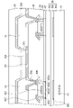
図1は、本発明の実施形態に係る有機EL(Electroluminescence)表示装置の平面図である。有機EL表示装置は、基板10と、フレキシブルプリント基板12と、フレキシブルプリント基板12上に配置される集積回路パッケージ14とを含む。この実施形態における有機EL表示装置は、屈曲が可能なシートディスプレイまたはフレキシブルディスプレイである。
FIG. 1 is a plan view of an organic EL (Electroluminescence) display device according to an embodiment of the present invention. The organic EL display device includes a
基板10は、表示領域42及び表示領域42を囲む周辺領域46を含む。周辺領域46は表示領域42の外側にある。表示領域42内には複数の単位画素44が配置されている。有機EL表示装置は、例えば、赤、緑及び青からなる複数色の単位画素(サブピクセル)を組み合わせて、フルカラーの画素を形成し、フルカラーの画像を表示するようになっている。基板10のうち一方向の端には、フレキシブルプリント基板12が接続されている。集積回路パッケージ14には、単位画素44に含まれる画素回路を駆動する駆動回路のうち一部が搭載される。また、基板10上の周辺領域46にも駆動回路の一部が配置される。
The
図2は、図1に示す有機EL表示装置のII-II切断線における断面図である。基板10(アレイ基板)の材料はポリイミドであるが、シートディスプレイ又はフレキシブルディスプレイを構成するために十分な可撓性を有する基材であれば他の樹脂材料を用いても良い。 FIG. 2 is a cross-sectional view taken along the line II-II of the organic EL display device shown in FIG. The material of the substrate 10 (array substrate) is polyimide, but other resin materials may be used as long as the substrate has sufficient flexibility to form a sheet display or a flexible display.
基板10上に、酸化シリコンを含む第1の下地層20aが設けられている。また、第1の下地層20aの上には、窒化シリコンを含む第2の下地層20bが設けられている。そして、第1の下地層20aと第2の下地層20bとの間には、平面視で互いに離間する複数の電界抑制膜205が設けられている。平面視で第1の下地層20aおよび第2の下地層20bは、基板10の略全域に設けられており、少なくとも表示領域42の全域と重なる。電界抑制膜205は、基板10の略全域に設けられているわけではなく、表示領域42の全域と重なるわけではない。図2に示すように、複数個の電界抑制膜205が互いに離間して設けられている。電界抑制膜205の側面は第2の下地層20bで覆われており、また平面視で、第1の下地層20aと第2の下地層20bとは一部において直接的に接する。電界抑制膜205は薄膜トランジスタの位置と重なるように設けられている。その配置の詳細については後述する。第2の下地層20bの上には酸化シリコンを含む第3の下地層20cが設けられる。
A
第1の下地層20aは、基板10との密着性を向上させ、第2の下地層20bは、外部からの水分及び不純物をブロックし、第3の下地層20cは第2の下地層20b中に含有する水素原子が上部にある薄膜トランジスタの半導体膜403側に拡散しないようにブロックする。この3層をまとめて下地層20とよぶ。下地層20は、特にこの三層積層構造に限定するものではなく、さらに層が積層されても良いし、単層あるいは二層積層としても良い。下地層20の厚さは、500nm以上1000nm未満である。
The
下地層20の上には複数の薄膜トランジスタが形成されている。薄膜トランジスタのそれぞれは、ゲート電極401と、半導体膜403と、ソース電極405と、ドレイン電極407とを含む。半導体膜403は下地層20の上に設けられる。半導体膜403はポリシリコンであるが、透明酸化物半導体(TAOS: Transparent Amorphous Oxide Semiconductor)であってもよい。半導体膜403の上には、酸化シリコンを含む第1の絶縁層22が設けられ、第1の絶縁層22の上には、平面視で半導体膜403と重畳するゲート電極401を含む第1の導電層が設けられている。ゲート電極401の上には、窒化シリコンを含む第2の絶縁層24および酸化シリコンを含む第3の絶縁層26が順に設けられる。第2の絶縁層と第3の絶縁層26との一方は、省略してもよい。第1の絶縁層22から第3の絶縁層26は、他の絶縁性のある材質により構成されてもよい。第3の絶縁層26の上には、ソース電極405およびドレイン電極407を含む第2の導電層が設けられる。第1の絶縁層22はいわゆるゲート絶縁膜として設けられている。第1の導電層は、例えばMoWにより形成される。第2の導電層は、例えば、Ti、Al及びTiの三層積層構造である。
A plurality of thin film transistors are formed on the
半導体膜403は、ゲート電極401に重畳するチャネル領域403cと、チャネル領域403cを挟むソース領域403sおよびドレイン領域403dを有する。半導体膜403のうち、チャネル領域403cとソース領域403sおよびドレイン領域403dとの間に、低濃度不純物領域が設けられてよい。第1の絶縁層22、第2の絶縁層24および第3の絶縁層26には、それぞれ半導体膜403のソース領域403sおよびドレイン領域403dの上面に達する2つのコンタクトホールが形成されており、コンタクトホールのそれぞれの中にはソース電極405およびドレイン電極407が設けられている。ソース電極405はソース領域403sと電気的に接続し、ドレイン電極407はドレイン領域403dと電気的に接続する。ドレイン電極407は画素回路を構成する配線(に接続され、ソース電極405画素電極301に接続される。
The
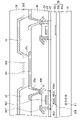
ここで、電界抑制膜205は、下地層20を構成する窒化シリコンや酸化シリコンより比誘電率が高く、またこれらより絶縁性の強いアルミナ(酸化アルミニウム)により形成されている。また、電界抑制膜205は、酸化アルミニウムをALD(Atomic Layer Deposition)法で積層することにより形成されている。ALD法により、緻密なアルミナの膜を形成することができ、電界抑制膜205の誘電率や絶縁性をより高くすることができる。電界抑制膜205はスパッタ法などにより形成されてもよい。電界抑制膜205の厚さは10nm以上100nm以下である。電界抑制膜205は、平面視で半導体膜403のチャネル領域403cを覆っている。また、電界抑制膜205は、平面視で半導体膜403とゲート電極401とが重畳する領域を覆っている構造でもよい。電界抑制膜205は、チャネル領域403cの延伸方向でみて半導体膜403のソース領域403s側の端およびドレイン領域403d側の端より内側に配置される。換言すれば、電界抑制膜205の薄膜トランジスタのチャネル長の方向の長さは、該チャネル長の長さ以上であり、記半導体膜403の該チャネル長の方向の長さよりも小さい。
Here, the electric
誘電率が高い材料は、電界がかかると分極し、その電界を弱める。本実施形態では、ポリミイドのような有機材料を用いた基板10は、製造過程や製造後の使用により電荷81を貯める性質がある。この電荷81を貯める現象をチャージアップと呼ぶ。電界抑制膜205により、電荷81により半導体膜403にかかる電界を弱めることができる。これにより、電荷81に起因する薄膜トランジスタの特性の変動を抑えることができる。なお、電界抑制膜205を用いる代わりに下地層20を厚くすることによっても薄膜トランジスタの特性の変動を抑えることができるが、表示装置全体の厚み、或いはパネルの厚みが増加する。電界抑制膜205を用いることで、下地層20の厚さを抑えつつ、換言すれば表示装置全体の厚さ増加を抑えつつ、電荷81に起因する薄膜トランジスタの特性の変動を抑えることができる。また、電界抑制膜205は、絶縁性が高いため、薄膜トランジスタから基板10への電荷の移動を抑えることができ、それによっても電荷の影響を抑えることができる。
A material with a high dielectric constant is polarized when an electric field is applied, weakening the electric field. In the present embodiment, the
図3は、有機EL表示装置の比較例を示す断面図である。図2の例では、ソース電極405およびドレイン電極407より上の層の記載を省略している。図3の例では、電界抑制膜205が設けられていない。この場合、基板10に蓄積された電荷81により生じる電界が本実施形態に比べて抑制されずに半導体膜403に及ぼされる。これにより、薄膜トランジスタの特性の変動がより起きやすくなる。
FIG. 3 is a cross-sectional view showing a comparative example of an organic EL display device. In the example of FIG. 2, the description of the layer above the
ここで、電界抑制膜205は、少なくともチャネル領域403cを覆っていればよく、図4に示すように、チャネル領域403cの延伸方向でみて半導体膜403のソース領域403s側の端およびドレイン領域403d側の端より外側にも配置されてもよい。ただし、電界抑制膜205に用いられるアルミナは硬い材料であるため、クラック等の発生を避けるためにそのサイズを小さくすることが望ましい。電界抑制膜205は、チャネル領域403cの延伸方向でみて半導体膜403のソース領域403s側の端およびドレイン領域403d側の端より内側に配置されることが望ましい。
Here, the electric
また、半導体膜403がポリシリコンである場合は、電子移動度が大きいため基板10内の電荷81の影響をより受けやすい。そのため、半導体膜403がポリシリコンの場合に電界抑制膜205を用いることがより好適であるが、半導体膜403が酸化物半導体であっても効果を得ることができる。
Further, when the
平坦化層30は、ソース電極405およびドレイン電極407を覆うように設けられる。平坦化層30としては、CVD(Chemical Vapor Deposition)等により形成される無機絶縁材料に比べ、表面の平坦性に優れることから、感光性アクリル等の有機材料が多く用いられる。
The
平坦化層30は、ソース電極405を露出させる開口30aを有する。また、この開口30aを介してソース電極405に導通する画素電極301が設けられている。画素電極301は、例えば、IZO(Indium Zinc Oxide)膜、Ag膜、IZO膜の三層積層構造であってよい。画素電極301は、開口30aの上端から側方に拡がっている。なお、ソース電極405の代わりにドレイン電極407が画素電極301に接続してもよい。
The
平坦化層30の上であって例えば開口30aの上方に、バンク32が形成されている。バンク32は平坦化層30と同じく絶縁性のある感光性アクリル等により形成される。バンク32は互いに隣接する単位画素44の間に設けられており、単位画素44が備える発光領域に対応する開口32aを有する、開口32aの側面はテーパ形状を有し、開口32aの底には画素電極301が露出している。画素電極301の上かつ開口32aの中には有機EL層303が設けられている。有機EL層303は、ホール注入層、ホール輸送層、発光層、電子輸送層、電子注入層を含む。これらの層は、蒸着によって形成されても良いし、塗布によって形成されてもよい。本図では、これらの層は開口32aの内部に形成されているが、少なくとも一部の層がバンク32の上に形成されてもよい。その一部の層は複数の単位画素44に跨って形成されてもよい。
A
有機EL層303の上には、対向電極305が設けられている。対向電極305は、例えば、有機EL層303からの出射光が透過する程度の薄膜として形成されるMgとAgとの合金で形成されてもよいし、ITOで形成されてもよい。対向電極305はバンク32の上にも設けられている。有機EL層303は、画素電極301と対向電極305との間を流れる電流により発光する。
A
対向電極305の上には、封止層34が設けられている。封止層34は、外部からの水分が有機EL層303に侵入することを防止する。封止層34は、例えば、シリコン窒化膜、有機樹脂層及びシリコン窒化膜の積層構造である。
A
なお、封止層34上にカバーガラスやタッチパネル基板等が設けられても良い。この場合、封止層34とカバーガラスやタッチパネル基板との間に、樹脂等の充填材が充填されてもよい。また、ポリイミド等の可撓性を有する基材を用いた対向基板が封止層34の上に配置されてもよい。
A cover glass, a touch panel substrate, or the like may be provided on the
ここで、折り曲げを容易にするために、下地層20および第1の絶縁層22から第3の絶縁層26は、一部の領域が除去されていてもよい。この場合、下地層20は互いに離間する複数の下地膜を含むが、下地膜のそれぞれは複数の電界抑制膜205を有してよい。表示領域を湾曲させる表示装置で、湾曲させる部分(湾曲部)が決まっている場合、電界抑制膜205を湾曲部には配置しない構造にしてもよい。電界抑制膜205に用いられるアルミナは硬い材料であるため、湾曲部には配置せず、非湾曲部には配置することで、フレキシブル性を維持しつつ、基板10に蓄積された電荷81による薄膜トランジスタの特性の変動を抑制するという、効果を得ることができる。
Here, in order to facilitate bending, a part of the
図2の例では、表示領域42内の単位画素44に用いられる薄膜トランジスタに本発明を適用する例について説明したが、周辺領域46上の駆動回路を構成する薄膜トランジスタに本発明が適用されてもよい。基板10上の周辺領域46に形成される薄膜トランジスタは、より多くの電流を流す必要があるため、一般的にポリシリコンを用いた薄膜トランジスタが配置される。単位画素44中と異なり酸化物半導体が用いられることが少ないため、電界抑制膜205を用いることでより確実に薄膜トランジスタの特性変動の抑制の効果を得ることができる。周辺領域46に形成される薄膜トランジスタのうち一部では、そのソース電極405およびドレイン電極407のうち一方が表示領域42内を延びる走査線に接続されており、その走査線は単位画素44を構成する薄膜トランジスタのゲート電極401に電気的に接続されている。もちろん、電界抑制膜205は、表示領域42内の薄膜トランジスタのみに設けられてもよいし、駆動回路を構成する薄膜トランジスタのみに設けられてもよい。また、電界抑制膜205は、表示領域42内の薄膜トランジスタおよび駆動回路を構成する薄膜トランジスタの両方に用いられてもよい。
In the example of FIG. 2, an example of applying the present invention to the thin film transistor used for the
図5は、図2に示す構造の変形例を示している。図5において、電界抑制膜205は、第2の下地層20bと第3の下地層20cとの間に位置している。図5に示す電界抑制膜205は、図2と同様に、チャネル領域403cの延伸方向でみて半導体膜403のソース領域403s側の端およびドレイン領域403d側の端より内側に配置されている。しかし、図4と同様に、チャネル領域403cの延伸方向でみて半導体膜403のソース領域403s側の端およびドレイン領域403d側の端より外側にも配置されてもよい。図5に示す構成においても、基板10に蓄積された電荷81による薄膜トランジスタの特性の変動を抑制することができる。
FIG. 5 shows a modified example of the structure shown in FIG. In FIG. 5, the electric
本発明は、上述した実施形態に限定されるものではなく種々の変形が可能である。例えば、実施形態で説明した構成は、実質的に同一の構成、同一の作用効果を奏する構成又は同一の目的を達成することができる構成で置き換えることができる。また、これまでに有機EL表示装置に本発明を適用する例について説明したが、例えば液晶表示装置など、有機材料を用いた基板を有する他の種類の表示装置にも本発明を適用できる。 The present invention is not limited to the above-described embodiment, and various modifications are possible. For example, the configurations described in the embodiments can be replaced with substantially the same configuration, a configuration that exhibits the same action and effect, or a configuration that can achieve the same purpose. Further, although an example of applying the present invention to an organic EL display device has been described so far, the present invention can also be applied to other types of display devices having a substrate using an organic material, such as a liquid crystal display device.
10 基板、12 フレキシブルプリント基板、14 集積回路パッケージ、20 下地層、20a 第1の下地層、20b 第2の下地層、20c 第3の下地層、22 第1の絶縁層、24 第2の絶縁層、26 第3の絶縁層、30 平坦化層、30a,32a 開口、32 バンク、34 封止層、42 表示領域、44 単位画素、46 周辺領域、81 電荷、205 電界抑制膜、301 画素電極、303 有機EL層、305 対向電極、401 ゲート電極、403 半導体膜、403c チャネル領域、403d ドレイン領域、403s ソース領域、405 ソース電極、407 ドレイン電極。 10 boards, 12 flexible printed boards, 14 integrated circuit packages, 20 base layers, 20a first base layer, 20b second base layer, 20c third base layer, 22 first insulation layer, 24 second insulation. Layer, 26 Third insulating layer, 30 Flattening layer, 30a, 32a opening, 32 banks, 34 encapsulation layer, 42 display area, 44 unit pixels, 46 peripheral areas, 81 charges, 205 electric field suppression film, 301 pixel electrodes , 303 organic EL layer, 305 counter electrode, 401 gate electrode, 403 semiconductor film, 403c channel region, 403d drain region, 403s source region, 405 source electrode, 407 drain electrode.
Claims (13)
前記基板の上に設けられる第1の下地膜と、
前記第1の下地膜の上方に設けられる薄膜トランジスタと、
前記薄膜トランジスタに備えられ、チャネル領域を有する半導体膜と、
前記第1の下地膜と前記半導体膜との間に設けられ、平面視で前記チャネル領域と重なる電界抑制膜と、を含み、
前記電界抑制膜は、前記第1の下地膜よりも誘電率が高く、
前記薄膜トランジスタを複数有し、
前記電界抑制膜を複数有し、
複数の前記電界抑制膜の各々は、複数の前記薄膜トランジスタうちの、互いに異なる1つの薄膜トランジスタと平面視で重なる、
表示装置。 Substrates containing organic materials and
The first base film provided on the substrate and
A thin film transistor provided above the first substrate film and
A semiconductor film provided in the thin film transistor and having a channel region,
An electric field suppression film provided between the first base film and the semiconductor film and overlapping the channel region in a plan view is included.
The electric field suppression film has a higher dielectric constant than the first base film, and has a higher dielectric constant.
Having a plurality of the thin film transistors
Having a plurality of the electric field suppression films,
Each of the plurality of electric field suppression films overlaps with one thin film transistor different from each other in a plan view among the plurality of the thin film transistors.
Display device.
前記電界抑制膜はアルミナを含む、
表示装置。 In the display device according to claim 1,
The electric field suppression film contains alumina.
Display device.
前記第1の下地膜は、窒化シリコンおよび酸化シリコンの少なくとも一方を含み、
前記電界抑制膜の誘電率は、窒化シリコンの誘電率及び酸化シリコンの誘電率よりも高い、表示装置。 In the display device according to claim 1 or 2.
The first base film contains at least one of silicon nitride and silicon oxide, and the first base film contains at least one of silicon nitride and silicon oxide.
A display device in which the dielectric constant of the electric field suppression film is higher than the dielectric constant of silicon nitride and the dielectric constant of silicon oxide.
前記第1の下地膜と前記半導体膜との間に、第2の下地膜が位置し、
前記電界抑制膜は、前記第1の下地膜と前記第2の下地膜との間に位置する、表示装置。 In the display device according to any one of claims 1 to 3.
A second base film is located between the first base film and the semiconductor film, and the second base film is located.
The electric field suppression film is a display device located between the first base film and the second base film.
前記第1の下地膜は、酸化シリコンを含み、
前記第2の下地膜は、窒化シリコンを含み、
前記第1の下地膜と前記第2の下地膜とは、直に接する、表示装置。 In the display device according to claim 4,
The first base film contains silicon oxide and contains silicon oxide.
The second base film contains silicon nitride and contains silicon nitride.
A display device in which the first base film and the second base film are in direct contact with each other.
前記第1の下地膜の上に第2の下地膜が位置し、
前記第2の下地膜の上に第3の下地膜が位置し、
前記第3の下地膜の上に、前記第3の下地膜と直に接して前記半導体膜が位置し、
前記電界抑制膜は、前記第2の下地膜と前記第3の下地膜との間に位置する、表示装置。 In the display device according to any one of claims 1 to 3.
The second base film is located on the first base film,
The third base film is located on the second base film,
The semiconductor film is located on the third base film in direct contact with the third base film.
The electric field suppression film is a display device located between the second base film and the third base film.
前記第2の下地膜は、窒化シリコンを含み、
前記第3の下地膜は、酸化シリコンを含む、表示装置。 In the display device according to claim 6,
The second base film contains silicon nitride and contains silicon nitride.
The third base film is a display device containing silicon oxide.
前記半導体膜は、ソース領域とドレイン領域とを有し、
前記電界抑制膜は、前記チャネル領域の延伸方向でみて前記ソース領域側の端および前記ドレイン領域側の端より内側に配置される、表示装置。 In the display device according to any one of claims 1 to 7.
The semiconductor film has a source region and a drain region, and has a source region and a drain region.
A display device in which the electric field suppression film is arranged inside the end on the source region side and the end on the drain region side when viewed in the stretching direction of the channel region.
前記基板上に、前記薄膜トランジスタを含む画素を有し、
前記電界抑制膜は、平面視で前記画素と重なる、表示装置。 In the display device according to any one of claims 1 to 8.
A pixel including the thin film transistor is provided on the substrate.
The electric field suppression film is a display device that overlaps with the pixels in a plan view.
前記基板上に、複数の画素を含む表示領域と、前記表示領域の外側に位置する周辺領域と、を有し、
前記周辺領域には、前記複数の画素を駆動する駆動回路が位置し、
前記薄膜トランジスタは、前記駆動回路に含まれ、
前記電界抑制膜は、前記周辺領域に位置する、表示装置。 In the display device according to any one of claims 1 to 8.
The substrate has a display area including a plurality of pixels and a peripheral area located outside the display area.
A drive circuit for driving the plurality of pixels is located in the peripheral region.
The thin film transistor is included in the drive circuit.
The electric field suppression film is a display device located in the peripheral region.
前記基板上に、複数の画素を含む表示領域を有し、
前記表示領域に、前記基板が湾曲している湾曲部を有し、
前記電界抑制膜は、前記湾曲部に位置しない、表示装置。 In the display device according to any one of claims 1 to 10.
A display area including a plurality of pixels is provided on the substrate.
The display area has a curved portion in which the substrate is curved, and the display area has a curved portion.
The electric field suppression film is a display device that is not located at the curved portion.
前記電界抑制膜は、前記表示領域の前記湾曲部とは異なる部分に位置する、表示装置。 In the display device according to claim 11,
The electric field suppression film is a display device located at a portion different from the curved portion of the display region.
前記基板の上に設けられる第1の下地膜と、
前記第1の下地膜の上方に設けられる薄膜トランジスタと、
前記薄膜トランジスタに備えられ、チャネル領域を有する半導体膜と、
前記第1の下地膜と前記半導体膜との間に設けられ、平面視で前記チャネル領域と重なる電界抑制膜と、を含み、
前記電界抑制膜は、前記第1の下地膜よりも誘電率が高く、
前記基板上に、複数の画素を含む表示領域を有し、
前記表示領域に、前記基板が湾曲している湾曲部を有し、
前記電界抑制膜は、前記湾曲部に位置しない、表示装置。 Substrates containing organic materials and
The first base film provided on the substrate and
A thin film transistor provided above the first substrate film and
A semiconductor film provided in the thin film transistor and having a channel region,
An electric field suppression film provided between the first base film and the semiconductor film and overlapping the channel region in a plan view is included.
The electric field suppression film has a higher dielectric constant than the first base film, and has a higher dielectric constant.
A display area including a plurality of pixels is provided on the substrate.
The display area has a curved portion in which the substrate is curved, and the display area has a curved portion.
The electric field suppression film is a display device that is not located at the curved portion.
Priority Applications (3)
| Application Number | Priority Date | Filing Date | Title |
|---|---|---|---|
| JP2017237061A JP7086582B2 (en) | 2017-12-11 | 2017-12-11 | Display device |
| PCT/JP2018/038832 WO2019116720A1 (en) | 2017-12-11 | 2018-10-18 | Display device |
| US16/897,298 US11605690B2 (en) | 2017-12-11 | 2020-06-10 | Display device having an electric field infibition film |
Applications Claiming Priority (1)
| Application Number | Priority Date | Filing Date | Title |
|---|---|---|---|
| JP2017237061A JP7086582B2 (en) | 2017-12-11 | 2017-12-11 | Display device |
Publications (3)
| Publication Number | Publication Date |
|---|---|
| JP2019106426A JP2019106426A (en) | 2019-06-27 |
| JP2019106426A5 JP2019106426A5 (en) | 2021-01-21 |
| JP7086582B2 true JP7086582B2 (en) | 2022-06-20 |
Family
ID=66819158
Family Applications (1)
| Application Number | Title | Priority Date | Filing Date |
|---|---|---|---|
| JP2017237061A Active JP7086582B2 (en) | 2017-12-11 | 2017-12-11 | Display device |
Country Status (3)
| Country | Link |
|---|---|
| US (1) | US11605690B2 (en) |
| JP (1) | JP7086582B2 (en) |
| WO (1) | WO2019116720A1 (en) |
Citations (8)
| Publication number | Priority date | Publication date | Assignee | Title |
|---|---|---|---|---|
| JP2009158936A (en) | 2007-12-03 | 2009-07-16 | Semiconductor Energy Lab Co Ltd | Semiconductor device |
| JP2011009704A (en) | 2009-05-26 | 2011-01-13 | Seiko Epson Corp | Thin film device, flexible circuit board including thin film device, and method for manufacturing thin film device |
| JP2012216796A (en) | 2011-03-30 | 2012-11-08 | Semiconductor Energy Lab Co Ltd | Manufacturing method for semiconductor device |
| US20160218305A1 (en) | 2015-01-28 | 2016-07-28 | Samsung Display Co., Ltd. | Display device |
| JP2017049568A (en) | 2015-08-31 | 2017-03-09 | 株式会社Joled | Semiconductor device, display, manufacturing method of display, and electronic apparatus |
| JP2017120775A (en) | 2015-12-30 | 2017-07-06 | エルジー ディスプレイ カンパニー リミテッド | Flexible organic light-emitting diode display device |
| JP2017212038A (en) | 2016-05-23 | 2017-11-30 | 株式会社ジャパンディスプレイ | Display device |
| JP2018129430A (en) | 2017-02-09 | 2018-08-16 | 株式会社ジャパンディスプレイ | Semiconductor device |
Family Cites Families (45)
| Publication number | Priority date | Publication date | Assignee | Title |
|---|---|---|---|---|
| US6449022B1 (en) * | 1999-04-16 | 2002-09-10 | Nec Corporation | Liquid crystal display |
| JP2001148480A (en) * | 1999-11-18 | 2001-05-29 | Nec Corp | Thin film transistor and device and method for manufacturing the same |
| TW494447B (en) * | 2000-02-01 | 2002-07-11 | Semiconductor Energy Lab | Semiconductor device and manufacturing method thereof |
| TW548860B (en) * | 2001-06-20 | 2003-08-21 | Semiconductor Energy Lab | Light emitting device and method of manufacturing the same |
| TWI253179B (en) * | 2002-09-18 | 2006-04-11 | Sanyo Electric Co | Method for making a semiconductor device |
| JP4095518B2 (en) * | 2002-10-31 | 2008-06-04 | セイコーエプソン株式会社 | Electro-optical device and electronic apparatus |
| JP4341062B2 (en) * | 2003-02-12 | 2009-10-07 | 日本電気株式会社 | Thin film transistor and manufacturing method thereof |
| TWI340607B (en) * | 2005-08-12 | 2011-04-11 | Au Optronics Corp | Organic electroluminescent display panel and fabricating method thereof |
| KR100824880B1 (en) * | 2006-11-10 | 2008-04-23 | 삼성에스디아이 주식회사 | Organic light emitting display device and manufacturing method thereof and moving device therefor |
| JP5458367B2 (en) * | 2007-07-09 | 2014-04-02 | Nltテクノロジー株式会社 | Thin film transistor and manufacturing method thereof |
| JP5402481B2 (en) * | 2009-09-30 | 2014-01-29 | カシオ計算機株式会社 | Display device, electronic apparatus, and display device manufacturing method |
| KR101975570B1 (en) * | 2012-11-06 | 2019-08-26 | 삼성디스플레이 주식회사 | Thin film transistor array panel and organic light emitting diode display including the same |
| KR102206412B1 (en) * | 2012-12-27 | 2021-01-22 | 엘지디스플레이 주식회사 | Thin film transistor, method for manufacturing the same and display device comprising the same |
| GB2517489A (en) * | 2013-08-23 | 2015-02-25 | Plastic Logic Ltd | Planarisation Layers |
| US9716134B2 (en) * | 2014-01-21 | 2017-07-25 | Apple Inc. | Organic light-emitting diode display with bottom shields |
| EP2963687B1 (en) * | 2014-07-03 | 2020-03-18 | LG Display Co., Ltd. | Organic electroluminescent device |
| KR102238994B1 (en) * | 2014-07-17 | 2021-04-12 | 엘지디스플레이 주식회사 | Display device |
| KR102182828B1 (en) * | 2014-08-14 | 2020-11-26 | 엘지디스플레이 주식회사 | Organic light emitting display panel |
| KR102183530B1 (en) * | 2014-08-14 | 2020-11-27 | 엘지디스플레이 주식회사 | Organic light emitting display panel |
| US9472605B2 (en) * | 2014-11-17 | 2016-10-18 | Apple Inc. | Organic light-emitting diode display with enhanced aperture ratio |
| US9397124B2 (en) * | 2014-12-03 | 2016-07-19 | Apple Inc. | Organic light-emitting diode display with double gate transistors |
| JP6553382B2 (en) | 2015-03-20 | 2019-07-31 | 株式会社ジャパンディスプレイ | Display device |
| CN105140260B (en) * | 2015-07-23 | 2018-04-17 | 京东方科技集团股份有限公司 | Organic LED array substrate and preparation method thereof, display device |
| TWI578509B (en) * | 2015-07-23 | 2017-04-11 | 友達光電股份有限公司 | Pixel structure |
| KR102373418B1 (en) * | 2015-08-31 | 2022-03-14 | 엘지디스플레이 주식회사 | Display Device |
| US9935165B2 (en) * | 2015-08-31 | 2018-04-03 | Joled, Inc. | Semiconductor device, display unit, method of manufacturing display unit, and electronic apparatus |
| KR102631445B1 (en) * | 2015-10-27 | 2024-01-31 | 삼성디스플레이 주식회사 | Organic light emitting diode display |
| KR102611499B1 (en) * | 2015-12-15 | 2023-12-06 | 엘지디스플레이 주식회사 | Flexible display device |
| CN105374882A (en) * | 2015-12-21 | 2016-03-02 | 武汉华星光电技术有限公司 | Low-temperature polycrystalline silicon thin film transistor and preparation method thereof |
| KR102536252B1 (en) * | 2016-03-25 | 2023-05-25 | 삼성디스플레이 주식회사 | Display apparatus and Method of manufacturing the same |
| US10141387B2 (en) * | 2016-04-08 | 2018-11-27 | Innolux Corporation | Display device |
| KR102561709B1 (en) * | 2016-07-25 | 2023-07-31 | 삼성디스플레이 주식회사 | Display device |
| KR102557892B1 (en) * | 2016-08-19 | 2023-07-21 | 삼성디스플레이 주식회사 | Display apparatus |
| JP2018031976A (en) * | 2016-08-26 | 2018-03-01 | 株式会社ジャパンディスプレイ | Display device |
| KR101857868B1 (en) * | 2016-08-26 | 2018-06-21 | 엘지디스플레이 주식회사 | Display Device |
| KR20180046418A (en) * | 2016-10-27 | 2018-05-09 | 엘지디스플레이 주식회사 | Display device and method for manufacturing of the same |
| KR20180061802A (en) * | 2016-11-30 | 2018-06-08 | 엘지디스플레이 주식회사 | Organic light emitting display device and method of manufacturing the same |
| KR20180061723A (en) * | 2016-11-30 | 2018-06-08 | 엘지디스플레이 주식회사 | Organic light emitting display device comprising multi-type thin film transistor |
| KR20180062284A (en) * | 2016-11-30 | 2018-06-08 | 엘지디스플레이 주식회사 | Organic light emitting diode display |
| JP2018116107A (en) * | 2017-01-17 | 2018-07-26 | 株式会社ジャパンディスプレイ | Display device |
| KR102352809B1 (en) * | 2017-03-31 | 2022-01-19 | 삼성디스플레이 주식회사 | Thin-film transistor substrate and display device including the same |
| CN107123666A (en) * | 2017-05-27 | 2017-09-01 | 上海天马微电子有限公司 | Display panel and display device |
| US10121830B1 (en) * | 2017-06-16 | 2018-11-06 | Wuhan China Star Optoelectronics Semiconductor Display Technology Co., Ltd. | OLED display panel and manufacturing method thereof |
| TWI630590B (en) * | 2017-07-05 | 2018-07-21 | Industrial Technology Research Institute | Pixel structure and display panel |
| US20190067338A1 (en) * | 2017-08-28 | 2019-02-28 | Wuhan China Star Optoelectronics Semiconductor Display Technology Co., Ltd. | Amoled Substrate and Method for Manufacturing Same |
-
2017
- 2017-12-11 JP JP2017237061A patent/JP7086582B2/en active Active
-
2018
- 2018-10-18 WO PCT/JP2018/038832 patent/WO2019116720A1/en active Application Filing
-
2020
- 2020-06-10 US US16/897,298 patent/US11605690B2/en active Active
Patent Citations (8)
| Publication number | Priority date | Publication date | Assignee | Title |
|---|---|---|---|---|
| JP2009158936A (en) | 2007-12-03 | 2009-07-16 | Semiconductor Energy Lab Co Ltd | Semiconductor device |
| JP2011009704A (en) | 2009-05-26 | 2011-01-13 | Seiko Epson Corp | Thin film device, flexible circuit board including thin film device, and method for manufacturing thin film device |
| JP2012216796A (en) | 2011-03-30 | 2012-11-08 | Semiconductor Energy Lab Co Ltd | Manufacturing method for semiconductor device |
| US20160218305A1 (en) | 2015-01-28 | 2016-07-28 | Samsung Display Co., Ltd. | Display device |
| JP2017049568A (en) | 2015-08-31 | 2017-03-09 | 株式会社Joled | Semiconductor device, display, manufacturing method of display, and electronic apparatus |
| JP2017120775A (en) | 2015-12-30 | 2017-07-06 | エルジー ディスプレイ カンパニー リミテッド | Flexible organic light-emitting diode display device |
| JP2017212038A (en) | 2016-05-23 | 2017-11-30 | 株式会社ジャパンディスプレイ | Display device |
| JP2018129430A (en) | 2017-02-09 | 2018-08-16 | 株式会社ジャパンディスプレイ | Semiconductor device |
Also Published As
| Publication number | Publication date |
|---|---|
| US11605690B2 (en) | 2023-03-14 |
| WO2019116720A1 (en) | 2019-06-20 |
| JP2019106426A (en) | 2019-06-27 |
| US20200303483A1 (en) | 2020-09-24 |
Similar Documents
| Publication | Publication Date | Title |
|---|---|---|
| US9922909B2 (en) | Display device | |
| US11508944B2 (en) | Display device | |
| US20210384451A1 (en) | Display device | |
| JP6456317B2 (en) | Display device and flexible display device | |
| KR20150041511A (en) | Display apparatus and method for manufacturing the same | |
| JP6726973B2 (en) | Display device | |
| CN106952934B (en) | Large-area mirror display device and manufacturing method thereof | |
| JP5253686B2 (en) | Active matrix substrate, display device, and method of manufacturing active matrix substrate | |
| US20190157609A1 (en) | Display device | |
| US10529274B2 (en) | Display device | |
| US10061419B2 (en) | Display device | |
| US20170205543A1 (en) | Mirror substrates, methods of manufacturing the same and display devices including the same | |
| CN112992989A (en) | Display panel and display device including the same | |
| CN109558029B (en) | Display device having touch structure and method of manufacturing the same | |
| JP7320407B2 (en) | Display device | |
| CN113130601A (en) | Display device | |
| JP2020068074A (en) | Display device | |
| US11137525B2 (en) | Display device and manufacturing method thereof | |
| JP7086582B2 (en) | Display device | |
| US20210408484A1 (en) | Electronic device | |
| US20170077457A1 (en) | Mirror display apparatus and method of manufacturing the same |
Legal Events
| Date | Code | Title | Description |
|---|---|---|---|
| A521 | Request for written amendment filed |
Free format text: JAPANESE INTERMEDIATE CODE: A523 Effective date: 20201203 |
|
| A621 | Written request for application examination |
Free format text: JAPANESE INTERMEDIATE CODE: A621 Effective date: 20201203 |
|
| A131 | Notification of reasons for refusal |
Free format text: JAPANESE INTERMEDIATE CODE: A131 Effective date: 20220201 |
|
| A521 | Request for written amendment filed |
Free format text: JAPANESE INTERMEDIATE CODE: A523 Effective date: 20220401 |
|
| TRDD | Decision of grant or rejection written | ||
| A01 | Written decision to grant a patent or to grant a registration (utility model) |
Free format text: JAPANESE INTERMEDIATE CODE: A01 Effective date: 20220517 |
|
| A61 | First payment of annual fees (during grant procedure) |
Free format text: JAPANESE INTERMEDIATE CODE: A61 Effective date: 20220608 |
|
| R150 | Certificate of patent or registration of utility model |
Ref document number: 7086582 Country of ref document: JP Free format text: JAPANESE INTERMEDIATE CODE: R150 |