JP7054967B2 - Resistance device, integrated circuit device, implantable device, and correction coefficient determination method - Google Patents
Resistance device, integrated circuit device, implantable device, and correction coefficient determination method Download PDFInfo
- Publication number
- JP7054967B2 JP7054967B2 JP2021567398A JP2021567398A JP7054967B2 JP 7054967 B2 JP7054967 B2 JP 7054967B2 JP 2021567398 A JP2021567398 A JP 2021567398A JP 2021567398 A JP2021567398 A JP 2021567398A JP 7054967 B2 JP7054967 B2 JP 7054967B2
- Authority
- JP
- Japan
- Prior art keywords
- voltage
- temperature
- transistor
- current
- value
- Prior art date
- Legal status (The legal status is an assumption and is not a legal conclusion. Google has not performed a legal analysis and makes no representation as to the accuracy of the status listed.)
- Active
Links
Images


Classifications
-
- A—HUMAN NECESSITIES
- A61—MEDICAL OR VETERINARY SCIENCE; HYGIENE
- A61N—ELECTROTHERAPY; MAGNETOTHERAPY; RADIATION THERAPY; ULTRASOUND THERAPY
- A61N1/00—Electrotherapy; Circuits therefor
- A61N1/02—Details
- A61N1/025—Digital circuitry features of electrotherapy devices, e.g. memory, clocks, processors
-
- H—ELECTRICITY
- H03—ELECTRONIC CIRCUITRY
- H03F—AMPLIFIERS
- H03F3/00—Amplifiers with only discharge tubes or only semiconductor devices as amplifying elements
- H03F3/45—Differential amplifiers
- H03F3/45071—Differential amplifiers with semiconductor devices only
- H03F3/45076—Differential amplifiers with semiconductor devices only characterised by the way of implementation of the active amplifying circuit in the differential amplifier
- H03F3/45475—Differential amplifiers with semiconductor devices only characterised by the way of implementation of the active amplifying circuit in the differential amplifier using IC blocks as the active amplifying circuit
-
- A—HUMAN NECESSITIES
- A61—MEDICAL OR VETERINARY SCIENCE; HYGIENE
- A61N—ELECTROTHERAPY; MAGNETOTHERAPY; RADIATION THERAPY; ULTRASOUND THERAPY
- A61N1/00—Electrotherapy; Circuits therefor
- A61N1/02—Details
- A61N1/08—Arrangements or circuits for monitoring, protecting, controlling or indicating
-
- G—PHYSICS
- G01—MEASURING; TESTING
- G01K—MEASURING TEMPERATURE; MEASURING QUANTITY OF HEAT; THERMALLY-SENSITIVE ELEMENTS NOT OTHERWISE PROVIDED FOR
- G01K7/00—Measuring temperature based on the use of electric or magnetic elements directly sensitive to heat ; Power supply therefor, e.g. using thermoelectric elements
-
- G—PHYSICS
- G05—CONTROLLING; REGULATING
- G05F—SYSTEMS FOR REGULATING ELECTRIC OR MAGNETIC VARIABLES
- G05F1/00—Automatic systems in which deviations of an electric quantity from one or more predetermined values are detected at the output of the system and fed back to a device within the system to restore the detected quantity to its predetermined value or values, i.e. retroactive systems
- G05F1/10—Regulating voltage or current
- G05F1/46—Regulating voltage or current wherein the variable actually regulated by the final control device is dc
- G05F1/56—Regulating voltage or current wherein the variable actually regulated by the final control device is dc using semiconductor devices in series with the load as final control devices
- G05F1/565—Regulating voltage or current wherein the variable actually regulated by the final control device is dc using semiconductor devices in series with the load as final control devices sensing a condition of the system or its load in addition to means responsive to deviations in the output of the system, e.g. current, voltage, power factor
- G05F1/567—Regulating voltage or current wherein the variable actually regulated by the final control device is dc using semiconductor devices in series with the load as final control devices sensing a condition of the system or its load in addition to means responsive to deviations in the output of the system, e.g. current, voltage, power factor for temperature compensation
-
- H—ELECTRICITY
- H03—ELECTRONIC CIRCUITRY
- H03K—PULSE TECHNIQUE
- H03K17/00—Electronic switching or gating, i.e. not by contact-making and –breaking
- H03K17/08—Modifications for protecting switching circuit against overcurrent or overvoltage
- H03K17/081—Modifications for protecting switching circuit against overcurrent or overvoltage without feedback from the output circuit to the control circuit
- H03K17/08104—Modifications for protecting switching circuit against overcurrent or overvoltage without feedback from the output circuit to the control circuit in field-effect transistor switches
-
- H—ELECTRICITY
- H03—ELECTRONIC CIRCUITRY
- H03F—AMPLIFIERS
- H03F2203/00—Indexing scheme relating to amplifiers with only discharge tubes or only semiconductor devices as amplifying elements covered by H03F3/00
- H03F2203/45—Indexing scheme relating to differential amplifiers
- H03F2203/45526—Indexing scheme relating to differential amplifiers the FBC comprising a resistor-capacitor combination and being coupled between the LC and the IC
-
- H—ELECTRICITY
- H03—ELECTRONIC CIRCUITRY
- H03F—AMPLIFIERS
- H03F2203/00—Indexing scheme relating to amplifiers with only discharge tubes or only semiconductor devices as amplifying elements covered by H03F3/00
- H03F2203/45—Indexing scheme relating to differential amplifiers
- H03F2203/45544—Indexing scheme relating to differential amplifiers the IC comprising one or more capacitors, e.g. coupling capacitors
-
- H—ELECTRICITY
- H03—ELECTRONIC CIRCUITRY
- H03K—PULSE TECHNIQUE
- H03K17/00—Electronic switching or gating, i.e. not by contact-making and –breaking
- H03K17/08—Modifications for protecting switching circuit against overcurrent or overvoltage
- H03K2017/0806—Modifications for protecting switching circuit against overcurrent or overvoltage against excessive temperature
Landscapes
- Health & Medical Sciences (AREA)
- Engineering & Computer Science (AREA)
- Public Health (AREA)
- General Health & Medical Sciences (AREA)
- Veterinary Medicine (AREA)
- General Physics & Mathematics (AREA)
- Biomedical Technology (AREA)
- Nuclear Medicine, Radiotherapy & Molecular Imaging (AREA)
- Radiology & Medical Imaging (AREA)
- Life Sciences & Earth Sciences (AREA)
- Animal Behavior & Ethology (AREA)
- Physics & Mathematics (AREA)
- Heart & Thoracic Surgery (AREA)
- Neurology (AREA)
- Electromagnetism (AREA)
- Radar, Positioning & Navigation (AREA)
- Automation & Control Theory (AREA)
- Power Engineering (AREA)
- Semiconductor Integrated Circuits (AREA)
Description
本発明は、抵抗デバイス、集積回路装置、体内埋込装置、及び、補正係数決定方法に関する。 The present invention relates to a resistance device, an integrated circuit device, an implantable device, and a method for determining a correction coefficient.
特許文献1に記載された増幅回路は、帰還抵抗としての電界効果トランジスタと、抵抗補正部とを備える。抵抗補正部は、温度変化による電界効果トランジスタのドレイン-ソース間の抵抗の変動を補正する。
The amplifier circuit described in
すなわち、電界効果トランジスタのゲート-ソース間の電圧Vgsが一定の場合、閾値電圧Vthが変化することにより、温度が高くなると、ドレイン-ソース間の抵抗Rdsは低くなる。一方、温度が低くなると、ドレイン-ソース間の抵抗Rdsは高くなる。そこで、抵抗補正部は、電圧Vgsと閾値電圧Vthとの差(Vgs-Vth)が一定値になるように、電界効果トランジスタのゲート端子に対して、閾値電圧Vth以下のゲート電圧Vgを印加して、電界効果トランジスタのドレイン-ソース間の抵抗Rdsが所定値になるように制御する。 That is, when the voltage Vgs between the gate and the source of the field effect transistor is constant, the resistance Rds between the drain and the source decreases as the temperature increases due to the change in the threshold voltage Vth. On the other hand, as the temperature decreases, the resistance Rds between the drain and the source increases. Therefore, the resistance correction unit applies a gate voltage Vg equal to or less than the threshold voltage Vth to the gate terminal of the field effect transistor so that the difference (Vgs-Vth) between the voltage Vgs and the threshold voltage Vth becomes a constant value. Therefore, the resistance Rds between the drain and the source of the field effect transistor is controlled to be a predetermined value.
具体的には、抵抗補正部は、温度検出部を有する。温度検出部は、温度変化に対して線形に変化する電圧又は電流を出力する。抵抗補正部は、温度検出部が出力する電流又は電圧に基づいて、電界効果トランジスタのドレイン-ソース間の抵抗Rdsが所定値になるように、電界効果トランジスタのゲート端子に対して、閾値電圧以下のゲート電圧Vgを印加する。 Specifically, the resistance correction unit has a temperature detection unit. The temperature detector outputs a voltage or current that changes linearly with respect to a temperature change. The resistance correction unit is below the threshold voltage with respect to the gate terminal of the field effect transistor so that the resistance Rds between the drain and the source of the field effect transistor becomes a predetermined value based on the current or voltage output by the temperature detection unit. The gate voltage Vg of is applied.
更に具体的には、抵抗補正部は、記憶部と、演算部とをさらに有する。記憶部は、温度検出部が出力する電流又は電圧と温度検出部の温度との関係を記憶している。また、記憶部は、温度検出部の温度と電界効果トランジスタのゲート端子に印加するゲート電圧Vgとの関係を記憶している。 More specifically, the resistance correction unit further includes a storage unit and a calculation unit. The storage unit stores the relationship between the current or voltage output by the temperature detection unit and the temperature of the temperature detection unit. Further, the storage unit stores the relationship between the temperature of the temperature detection unit and the gate voltage Vg applied to the gate terminal of the field effect transistor.
温度検出部が出力する電流又は電圧と温度検出部の温度との関係は、温度と、温度検出部が出力する電流又は電圧との関係を事前に測定して、記憶部に記憶される。温度検出部の温度と電界効果トランジスタのゲート端子に印加するゲート電圧Vgとの関係は、各温度において、電界効果トランジスタのゲート-ソース間の電圧Vgsと閾値電圧Vthとの差(Vgs-Vth)が一定値になるゲート電圧Vgが決定されて、記憶部に記憶される。 The relationship between the current or voltage output by the temperature detection unit and the temperature of the temperature detection unit is stored in the storage unit by measuring the relationship between the temperature and the current or voltage output by the temperature detection unit in advance. The relationship between the temperature of the temperature detector and the gate voltage Vg applied to the gate terminal of the field effect transistor is the difference between the gate-source voltage Vgs and the threshold voltage Vth of the field effect transistor (Vgs-Vth) at each temperature. The gate voltage Vg at which is a constant value is determined and stored in the storage unit.
演算部は、記憶部が記憶する温度検出部が出力する電流又は電圧と温度検出部の温度との関係を参照して、温度検出部が出力する電流又は電圧に基づいて、温度検出部の温度を求める。また、演算部は、記憶部が記憶する温度検出部の温度と電界効果トランジスタのゲート端子に印加するゲート電圧Vgとの関係を参照して、求めた温度に基づいて、電界効果トランジスタのゲート端子に印加するゲート電圧Vgを決定する。 The calculation unit refers to the relationship between the current or voltage output by the temperature detection unit stored in the storage unit and the temperature of the temperature detection unit, and the temperature of the temperature detection unit is based on the current or voltage output by the temperature detection unit. Ask for. Further, the arithmetic unit refers to the relationship between the temperature of the temperature detection unit stored in the storage unit and the gate voltage Vg applied to the gate terminal of the field effect transistor, and based on the obtained temperature, the gate terminal of the field effect transistor. The gate voltage Vg to be applied to is determined.
しかしながら、特許文献1には、電界効果トランジスタの電圧Vgsと閾値電圧Vthとの差(Vgs-Vth)が複数の異なる温度において一定値になるゲート電圧Vgの決定方法について何ら記載されていない。
However,
換言すれば、特許文献1には、電界効果トランジスタのドレイン-ソース間の抵抗Rds(電界効果トランジスタに関する物理量の一例)の温度依存性を低減して、抵抗Rdsが所定値になるようにゲート電圧Vgを補正するときの補正値の決定方法について何ら記載されていない。
In other words,
本発明の目的は、電界効果トランジスタに関する所望の物理量の温度依存性を低減するためにゲート-ソース間に印加する制御電圧を補正するときの補正係数と、電界効果トランジスタに関する所望の物理量との組み合わせを、効率良く決定できる抵抗デバイス、集積回路装置、体内埋込装置、及び、補正係数決定方法を提供することにある。 An object of the present invention is a combination of a correction coefficient for correcting a control voltage applied between a gate and a source in order to reduce the temperature dependence of a desired physical quantity for a field effect transistor and a desired physical quantity for a field effect transistor. It is an object of the present invention to provide a resistance device, an integrated circuit device, an implantable device, and a method for determining a correction coefficient, which can be efficiently determined.
本発明の一局面によれば、抵抗デバイスは、電界効果トランジスタと、電圧印加回路とを備える。電圧印加回路は、前記電界効果トランジスタのゲート-ソース間に、温度に応じた制御電圧を印加して、前記電界効果トランジスタのドレイン-ソース間の抵抗値を制御する。前記制御電圧は、基準電圧に補正電圧を加算した電圧を示す。前記補正電圧は、前記温度に依存し、第1温度でゼロになるように設定される。 According to one aspect of the invention, the resistance device comprises a field effect transistor and a voltage application circuit. The voltage application circuit applies a control voltage according to the temperature between the gate and the source of the field-effect transistor to control the resistance value between the drain and the source of the field-effect transistor. The control voltage indicates a voltage obtained by adding a correction voltage to a reference voltage. The correction voltage depends on the temperature and is set to be zero at the first temperature.
本発明の抵抗デバイスにおいて、前記電圧印加回路は、温度検出部と、制御電圧印加部とを含むことが好ましい。温度検出部は、前記温度に応じた検出信号を出力することが好ましい。制御電圧印加部は、前記検出信号に応じて前記温度に対して線形に変化する前記補正電圧を前記制御電圧が含むように、前記制御電圧を生成して、前記制御電圧を前記電界効果トランジスタのゲート-ソース間に印加することが好ましい。 In the resistance device of the present invention, the voltage application circuit preferably includes a temperature detection unit and a control voltage application unit. The temperature detection unit preferably outputs a detection signal corresponding to the temperature. The control voltage application unit generates the control voltage so that the control voltage includes the correction voltage that changes linearly with respect to the temperature in response to the detection signal, and the control voltage is applied to the field effect transistor of the field effect transistor. It is preferable to apply it between the gate and the source.
本発明の抵抗デバイスにおいて、前記第1温度は、前記補正電圧を定めるための係数である補正係数の変化に対して、前記電界効果トランジスタに関する物理量が略一定であるときの温度を示すことが好ましい。 In the resistance device of the present invention, the first temperature preferably indicates a temperature when the physical quantity of the field effect transistor is substantially constant with respect to a change in the correction coefficient, which is a coefficient for determining the correction voltage. ..
本発明の抵抗デバイスにおいて、前記補正電圧を定めるための係数である補正係数の値は、前記第1温度において前記電界効果トランジスタに関する目標物理量が得られるときの前記基準電圧に基づいて、前記第1温度と異なる第2温度において前記目標物理量が得られるときの値を示すことが好ましい。 In the resistance device of the present invention, the value of the correction coefficient, which is a coefficient for determining the correction voltage, is the first, based on the reference voltage when the target physical quantity for the field effect transistor is obtained at the first temperature. It is preferable to show the value when the target physical quantity is obtained at a second temperature different from the temperature.
本発明の抵抗デバイスにおいて、前記温度検出部は、第1電流を生成する第1電流源回路と、第2電流を生成する第2電流源回路とを含むことが好ましい。前記第1電流源回路の温度依存性と前記第2電流源回路の温度依存性とが異なることが好ましい。前記第1電流源回路と前記第2電流源回路とは、直列に接続されることが好ましい。前記第1電流と前記第2電流との差分電流が前記検出信号であることが好ましい。前記第1電流源回路が前記第1電流の電流値を変更し、及び/又は、前記第2電流源回路が前記第2電流の電流値を変更することで、前記第1温度が変更されることが好ましい。 In the resistance device of the present invention, the temperature detection unit preferably includes a first current source circuit that generates a first current and a second current source circuit that generates a second current. It is preferable that the temperature dependence of the first current source circuit and the temperature dependence of the second current source circuit are different. It is preferable that the first current source circuit and the second current source circuit are connected in series. It is preferable that the difference current between the first current and the second current is the detection signal. The first temperature is changed by the first current source circuit changing the current value of the first current and / or the second current source circuit changing the current value of the second current. Is preferable.
本発明の抵抗デバイスにおいて、前記電圧印加回路は、前記電界効果トランジスタのゲート-ソース間に前記制御電圧を印加して、前記電界効果トランジスタの第1動作領域におけるドレイン-ソース間の抵抗値を制御することが好ましい。前記第1動作領域は、前記電界効果トランジスタのゲート-ソース間の電圧の大きさが閾値電圧の大きさより大きい領域であることが好ましい。 In the resistance device of the present invention, the voltage application circuit applies the control voltage between the gate and the source of the field effect transistor to control the resistance value between the drain and the source in the first operating region of the field effect transistor. It is preferable to do so. The first operating region is preferably a region in which the magnitude of the voltage between the gate and the source of the field effect transistor is larger than the magnitude of the threshold voltage.
本発明の抵抗デバイスにおいて、前記電圧印加回路は、前記電界効果トランジスタのゲート-ソース間に前記制御電圧を印加して、前記電界効果トランジスタの第2動作領域におけるドレイン-ソース間の抵抗値を制御することが好ましい。前記第2動作領域は、前記電界効果トランジスタのゲート-ソース間の電圧の大きさが閾値電圧の大きさより小さい領域であることが好ましい。 In the resistance device of the present invention, the voltage application circuit applies the control voltage between the gate and the source of the field effect transistor to control the resistance value between the drain and the source in the second operating region of the field effect transistor. It is preferable to do so. The second operating region is preferably a region in which the magnitude of the voltage between the gate and the source of the field effect transistor is smaller than the magnitude of the threshold voltage.
本発明の他の局面によれば、集積回路装置は、上記抵抗デバイスの前記電界効果トランジスタ及び前記電圧印加回路を集積している。 According to another aspect of the present invention, the integrated circuit apparatus integrates the field effect transistor and the voltage application circuit of the resistance device.
本発明の更に他の局面によれば、体内埋込装置は、体内に埋め込まれる。体内埋込装置は、生体組織に刺激信号を与える刺激装置と生体信号を計測する計測装置とのうちの少なくとも1つを備える。前記刺激装置と前記計測装置とのうちの少なくとも1つは、上記の集積回路装置を含む。 According to yet another aspect of the invention, the implant device is implanted in the body. The implantable device includes at least one of a stimulator that gives a stimulus signal to a biological tissue and a measuring device that measures the biological signal. At least one of the stimulator and the measuring device includes the integrated circuit device described above.
本発明の更に他の局面によれば、補正係数決定方法は、電界効果トランジスタのゲート-ソース間に印加する制御電圧を補正するときの補正係数を決定する。補正係数決定方法では、次式において、前記制御電圧を「Vgs」で示し、基準電圧を「Vgs0」で示し、補正電圧を「Vc」で示し、補正係数を「β」で示し、変数としての温度を「T」で示し、前記補正電圧Vcがゼロになるときの温度である第1温度を「T1」で示す。補正係数決定方法は、前記第1温度T1において前記電界効果トランジスタに関する目標物理量が得られるときの前記基準電圧Vgs0の電圧値である特定電圧値を決定する工程と、前記第1温度T1と異なる第2温度及び前記基準電圧Vgs0の前記特定電圧値において前記目標物理量が得られるときの前記補正係数βの値である特定係数値を決定する工程とを含む。
Vgs=Vgs0+Vc=Vgs0+β(T-T1)According to still another aspect of the present invention, the correction coefficient determination method determines the correction coefficient when correcting the control voltage applied between the gate and the source of the field effect transistor. In the correction coefficient determination method, in the following equation, the control voltage is indicated by "Vgs", the reference voltage is indicated by "Vgs0", the correction voltage is indicated by "Vc", the correction coefficient is indicated by "β", and the variables are used. The temperature is indicated by "T", and the first temperature, which is the temperature at which the correction voltage Vc becomes zero, is indicated by "T1". The method for determining the correction coefficient is a step of determining a specific voltage value which is a voltage value of the reference voltage Vgs0 when a target physical quantity for the field effect transistor is obtained at the first temperature T1, and a second step different from the first temperature T1. 2. The step includes a step of determining a specific coefficient value which is a value of the correction coefficient β when the target physical quantity is obtained at the specific voltage value of the temperature and the reference voltage Vgs0.
Vgs = Vgs0 + Vc = Vgs0 + β (T-T1)
本発明の補正係数決定方法において、前記基準電圧Vgs0の前記特定電圧値を決定する前記工程は、前記第1温度T1において、前記基準電圧Vgs0の電圧値を変更しながら、前記電界効果トランジスタに関する物理量を計測する工程と、前記基準電圧Vgs0の前記電圧値を変更しながら計測された複数の前記物理量のうち、前記目標物理量と略一致する物理量を計測したときの前記基準電圧Vgs0の前記電圧値を前記基準電圧Vgs0の前記特定電圧値に決定する工程とを含むことが好ましい。前記補正係数βの前記特定係数値を決定する前記工程は、前記第2温度及び前記基準電圧Vgs0の前記特定電圧値において、前記補正係数βの値を変更しながら、前記電界効果トランジスタに関する物理量を計測する工程と、前記補正係数βの前記値を変更しながら計測された複数の前記物理量のうち、前記目標物理量と略一致する物理量を計測したときの前記補正係数βの前記値を前記補正係数βの前記特定係数値に決定する工程とを含むことが好ましい。 In the correction coefficient determination method of the present invention, the step of determining the specific voltage value of the reference voltage Vgs0 is a physical quantity relating to the electric field effect transistor while changing the voltage value of the reference voltage Vgs0 at the first temperature T1. And the voltage value of the reference voltage Vgs0 when measuring a physical amount that substantially matches the target physical quantity among the plurality of physical quantities measured while changing the voltage value of the reference voltage Vgs0. It is preferable to include a step of determining the specific voltage value of the reference voltage Vgs0. In the step of determining the specific coefficient value of the correction coefficient β, the physical quantity related to the electric field effect transistor is obtained while changing the value of the correction coefficient β at the second temperature and the specific voltage value of the reference voltage Vgs0. The correction coefficient is the value of the correction coefficient β when the physical quantity that substantially matches the target physical quantity is measured among the plurality of physical quantities measured while changing the value of the correction coefficient β and the step of measuring. It is preferable to include a step of determining the specific coefficient value of β.
本発明の補正係数決定方法において、前記第1温度T1は、前記補正係数βの変化に対して、前記電界効果トランジスタに関する物理量が略一定であるときの温度を示すことが好ましい。 In the correction coefficient determination method of the present invention, it is preferable that the first temperature T1 indicates the temperature when the physical quantity of the field effect transistor is substantially constant with respect to the change of the correction coefficient β.
本発明の補正係数決定方法において、前記補正電圧Vcは、第1電流と第2電流との差分電流に基づく値を有することが好ましい。前記第1電流は、温度の変化に対して線形に変化する電流を示すことが好ましい。前記第2電流は、前記温度の変化に対して線形に変化する電流を示すことが好ましい。前記第1電流の温度依存性と前記第2電流の温度依存性とが異なることが好ましい。補正係数決定方法は、前記第1電流の電流値と前記第2電流の電流値とのうちの少なくとも一方の電流値を変更することで、前記第1温度T1を変更する工程をさらに含むことが好ましい。 In the correction coefficient determining method of the present invention, the correction voltage Vc preferably has a value based on the difference current between the first current and the second current. It is preferable that the first current indicates a current that changes linearly with a change in temperature. It is preferable that the second current indicates a current that changes linearly with the change in temperature. It is preferable that the temperature dependence of the first current and the temperature dependence of the second current are different. The method for determining the correction coefficient may further include a step of changing the first temperature T1 by changing at least one of the current value of the first current and the current value of the second current. preferable.
本発明の補正係数決定方法において、前記目標物理量は、前記電界効果トランジスタを含む電子回路から計測可能な、前記電界効果トランジスタの抵抗値を含む物理量であって、目標値として設定される物理量を示すことが好ましい。 In the correction coefficient determination method of the present invention, the target physical quantity is a physical quantity including the resistance value of the field effect transistor, which can be measured from an electronic circuit including the field effect transistor, and indicates a physical quantity set as a target value. Is preferable.
本発明によれば、電界効果トランジスタに関する所望の物理量の温度依存性を低減するためにゲート-ソース間に印加する制御電圧を補正するときの補正係数と、電界効果トランジスタに関する所望の物理量との組み合わせを、効率良く決定できる抵抗デバイス、集積回路装置、体内埋込装置、及び、補正係数決定方法を提供できる。 According to the present invention, a combination of a correction coefficient for correcting a control voltage applied between a gate and a source in order to reduce the temperature dependence of a desired physical quantity for a field effect transistor and a desired physical quantity for a field effect transistor. Can be provided with a resistance device, an integrated circuit device, an implantable device, and a method for determining a correction coefficient.
以下、本発明の実施形態について、図面を参照しながら説明する。なお、図中、同一または相当部分については同一の参照符号を付して説明を繰り返さない。また、電流に付する参照符号を電流の「電流値」を表す符号として使用する場合があり、電圧に付する参照符号を電圧の「電圧値」を表す符号として使用する場合があり、抵抗又は抵抗素子に付する参照符号を抵抗又は抵抗素子の「抵抗値」を表す符号として使用する場合がある。さらに、複数の数式中の同一記号は、同一定義を有するため、同一記号の説明は適宜省略する。なお、図面において、理解の容易のために、ゲート端子を「g」で示し、ドレイン端子を「d」で示し、ソース端子を「s」で示す場合がある。 Hereinafter, embodiments of the present invention will be described with reference to the drawings. In the figure, the same or corresponding parts are designated by the same reference numerals and the description is not repeated. In addition, the reference code attached to the current may be used as a code representing the "current value" of the current, and the reference code attached to the voltage may be used as the code representing the "voltage value" of the voltage. The reference code attached to the resistance element may be used as a code indicating the resistance or the "resistance value" of the resistance element. Further, since the same symbol in a plurality of mathematical expressions has the same definition, the description of the same symbol will be omitted as appropriate. In the drawings, for ease of understanding, the gate terminal may be indicated by "g", the drain terminal may be indicated by "d", and the source terminal may be indicated by "s".
(実施形態1)
図1~図23(b)を参照して、本発明の実施形態1に係る抵抗デバイス100を説明する。(Embodiment 1)
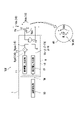
The
図1は、実施形態1に係る抵抗デバイス100を示す図である。図1に示すように、抵抗デバイス100は、電界効果トランジスタTNと、電圧印加回路1とを備える。図1に示すように、実施形態1では、電界効果トランジスタTNは、N型電界効果トランジスタである。具体的には、電界効果トランジスタTNは、n型MOSFET(n-type Metal-Oxide-Semiconductor Field-Effect Transistor)、つまり、NMOSトランジスタである。
FIG. 1 is a diagram showing a
以下、電界効果トランジスタTNを「トランジスタTN」と記載する場合がある。 Hereinafter, the field effect transistor TN may be referred to as “transistor TN”.
なお、電界効果トランジスタTNのバックゲート端子が、電界効果トランジスタTNのソース端子又はドレイン端子に接続されていてもよいし、アース又はグラウンドに接続されていてもよい。 The back gate terminal of the field-effect transistor TN may be connected to the source terminal or drain terminal of the field-effect transistor TN, or may be connected to ground or ground.
電界効果トランジスタTNは、抵抗素子として機能する。具体的には、電界効果トランジスタTNは、電界効果トランジスタTNのドレイン-ソース間の抵抗を利用することで抵抗素子として機能する。つまり、電界効果トランジスタTNはMOS抵抗として機能する。電界効果トランジスタがMOS抵抗として機能することは、例えば、「C.A.Mead, "Analog VLSI and Neural Systems", Addison-Wesley Publishing Company, 1989.」、又は、「T. Delbruck and C.A. Mead, "Adaptive photoreceptor with wide dynamic range", Proceedings of IEEE International Symposium on Circuits and Systems, 1994.」に記載されている。 The field effect transistor TN functions as a resistance element. Specifically, the field-effect transistor TN functions as a resistance element by utilizing the resistance between the drain and the source of the field-effect transistor TN. That is, the field effect transistor TN functions as a MOS resistor. Field-effect transistors can function as MOS resistors, for example, in "C.A. Mead," Analog VLSI and Neural Systems ", Addison-Wesley Publishing Company, 1989." or "T. Delbruck and C.A. Mead," Adaptive lithography with. Wide dynamic range ", Proceedings of IEEE International Symposium on Circuits and Systems, 1994."
具体的には、電界効果トランジスタTNは、電界効果トランジスタTNのゲート-ソース間の電圧が閾値電圧よりも大きい領域(線形領域及び飽和領域)におけるドレイン-ソース間の抵抗を利用することで抵抗素子として機能する。また、電界効果トランジスタTNは、電界効果トランジスタTNのゲート-ソース間の電圧が閾値電圧よりも小さい領域(サブスレッショルド領域)におけるドレイン-ソース間の抵抗を利用することで抵抗素子として機能する。 Specifically, the field-effect transistor TN is a resistance element by utilizing the resistance between the drain and the source in the region (linear region and saturation region) where the gate-source voltage of the field-effect transistor TN is larger than the threshold voltage. Functions as. Further, the field effect transistor TN functions as a resistance element by utilizing the resistance between the drain and the source in the region (subthreshold region) where the voltage between the gate and the source of the field effect transistor TN is smaller than the threshold voltage.
図1の領域AR内には、電界効果トランジスタTNがMOS抵抗MRとして機能するときの等価回路が示される。MOS抵抗MRは、電界効果トランジスタTNのドレイン-ソース間の抵抗値に相当する抵抗値Rを有する。電界効果トランジスタTNのドレイン-ソース間の電圧に相当する電圧VdsがMOS抵抗MRに印加されると、MOS抵抗MRには、電界効果トランジスタTNのドレイン-ソース間に流れるドレイン電流に相当する電流Idsが流れる。 In the region AR of FIG. 1, an equivalent circuit when the field effect transistor TN functions as a MOS resistance MR is shown. The MOS resistance MR has a resistance value R corresponding to the resistance value between the drain and the source of the field effect transistor TN. When a voltage Vds corresponding to the voltage between the drain and the source of the field effect transistor TN is applied to the MOS resistance MR, the current Ids corresponding to the drain current flowing between the drain and the source of the field effect transistor TN is applied to the MOS resistance MR. Flows.
以下、電界効果トランジスタTNのドレイン-ソース間の抵抗値Rを「電界効果トランジスタTNの抵抗値R」と記載する場合がある。 Hereinafter, the resistance value R between the drain and the source of the field effect transistor TN may be described as “the resistance value R of the field effect transistor TN”.
電圧印加回路1は、電界効果トランジスタTNのゲート-ソース間に、温度Tに応じた制御電圧Vgsを印加して、電界効果トランジスタTNのドレイン-ソース間の抵抗値Rを制御する。「電界効果トランジスタTNのゲート-ソース間」とは、「電界効果トランジスタTNのゲート端子とソース端子との間」のことである。温度Tは、抵抗デバイス100の周囲温度を示す。制御電圧Vgsは正の値を有する。制御電圧Vgsは、電界効果トランジスタTNのゲート-ソース間の電圧を示す。
The
以下、制御電圧Vgsを「ゲート-ソース電圧Vgs」と記載する場合がある。また、ドレイン-ソース間の電圧Vdsを「ドレイン-ソース電圧Vds」と記載する場合がある。 Hereinafter, the control voltage Vgs may be referred to as “gate-source voltage Vgs”. Further, the voltage Vds between the drain and the source may be described as "drain-source voltage Vds".
制御電圧Vgsは、基準電圧Vgs0に補正電圧Vcを加算した電圧を示す。具体的には、制御電圧Vgsは、式(1)によって表される。 The control voltage Vgs indicates a voltage obtained by adding the correction voltage Vc to the reference voltage Vgs0. Specifically, the control voltage Vgs is expressed by the equation (1).
Vgs=Vgs0+Vc …(1) Vgs = Vgs0 + Vc ... (1)
補正電圧Vcは、電界効果トランジスタTNに関する所望の物理量の温度依存性を低減するために、基準電圧Vgs0に加算される電圧である。 The correction voltage Vc is a voltage added to the reference voltage Vgs0 in order to reduce the temperature dependence of a desired physical quantity with respect to the field effect transistor TN.
電界効果トランジスタTNに関する物理量は、電界効果トランジスタTNを含む電子回路から計測可能な、電界効果トランジスタTNの抵抗値Rを含む物理量である。電界効果トランジスタTNに関する物理量は、例えば、電界効果トランジスタTNのドレイン-ソース間の抵抗値R、又は、電界効果トランジスタTNを含むフィルタ回路の遮断周波数fcである。「抵抗値Rを含む物理量」は、抵抗値Rに依存する物理量を示す。以下、電界効果トランジスタTNに関する所望の物理量を「目標物理量」と記載する場合がある。従って、目標物理量は、電界効果トランジスタTNを含む電子回路から計測可能な、電界効果トランジスタTNの抵抗値Rを含む物理量であって、目標値として設定される物理量を示す。 The physical quantity relating to the field effect transistor TN is a physical quantity including the resistance value R of the field effect transistor TN, which can be measured from an electronic circuit including the field effect transistor TN. The physical quantity of the field-effect transistor TN is, for example, the resistance value R between the drain and the source of the field-effect transistor TN, or the cutoff frequency fc of the filter circuit including the field-effect transistor TN. The "physical quantity including the resistance value R" indicates a physical quantity depending on the resistance value R. Hereinafter, a desired physical quantity relating to the field effect transistor TN may be described as a “target physical quantity”. Therefore, the target physical quantity is a physical quantity including the resistance value R of the field effect transistor TN, which can be measured from an electronic circuit including the field effect transistor TN, and indicates a physical quantity set as a target value.
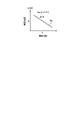
具体的には、補正電圧Vcは、式(2)によって示される。式(2)において、βは補正係数を示し、Tは温度を示し、T1は第1温度を示す。補正係数βは、補正電圧Vcを定めるための係数である。実施形態1では、補正係数βは、負の値を有する。従って、補正電圧Vcは、温度Tが高くなる程小さくなる。具体的には、補正係数βは、電界効果トランジスタTNに関する所望の物理量の温度依存性を低減するために、電界効果トランジスタTNのゲート-ソース間に印加する制御電圧Vgsを補正するときの係数である。 Specifically, the correction voltage Vc is represented by the equation (2). In equation (2), β indicates a correction coefficient, T indicates a temperature, and T1 indicates a first temperature. The correction coefficient β is a coefficient for determining the correction voltage Vc. In the first embodiment, the correction coefficient β has a negative value. Therefore, the correction voltage Vc becomes smaller as the temperature T becomes higher. Specifically, the correction coefficient β is a coefficient for correcting the control voltage Vgs applied between the gate and the source of the field effect transistor TN in order to reduce the temperature dependence of a desired physical quantity with respect to the field effect transistor TN. be.
Vc=β(T-T1) …(2) Vc = β (T-T1) ... (2)
式(2)に示すように、補正電圧Vcは、温度Tに依存し、第1温度T1でゼロになるように設定される。換言すれば、第1温度T1は、補正電圧Vcがゼロになるときの温度である。従って、実施形態1によれば、第1温度T1では補正の効果が無くなる。第1温度T1で補正の効果が無くなるような電圧印加回路1を利用することで、電界効果トランジスタTNのゲート-ソース間に印加する制御電圧Vgsを補正するときの補正係数βと、電界効果トランジスタTNに関する所望の物理量との組み合わせを、効率良く決定できる。この点の詳細は後述する。
As shown in the equation (2), the correction voltage Vc depends on the temperature T and is set to be zero at the first temperature T1. In other words, the first temperature T1 is the temperature at which the correction voltage Vc becomes zero. Therefore, according to the first embodiment, the correction effect is lost at the first temperature T1. By using the
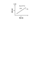
図2は、補正電圧Vcを示すグラフである。縦軸は補正電圧Vc[V]を示し、横軸は温度T[K]を示す。図2に示すように、補正電圧Vcは、温度Tに対して線形に変化する。補正電圧Vcを示す直線の傾きが補正係数βを示す。 FIG. 2 is a graph showing the correction voltage Vc. The vertical axis shows the correction voltage Vc [V], and the horizontal axis shows the temperature T [K]. As shown in FIG. 2, the correction voltage Vc changes linearly with respect to the temperature T. The slope of the straight line indicating the correction voltage Vc indicates the correction coefficient β.
次に、図3~図6を参照して、式(1)に示す制御電圧Vgsのように、基準電圧Vgs0に式(2)に示す温度Tに応じて線形に変化する補正電圧Vcを加算することでMOS抵抗MRとしての電界効果トランジスタTNの温度依存性を補正できる理由を説明する。この場合、理解を容易にするために、NOMSトランジスタの「Vgs>Vth」領域におけるドレイン-ソース間の抵抗値Rに着目する。「Vgs>Vth」領域とは、ゲート-ソース電圧Vgs(ゲート-ソース間の電圧)の大きさが閾値電圧Vthの大きさより大きいときのNOMSトランジスタの動作領域のことである。「Vgs>Vth」領域は、「電界効果トランジスタの第1動作領域」の一例に相当する。 Next, with reference to FIGS. 3 to 6, a correction voltage Vc that changes linearly according to the temperature T shown in the equation (2) is added to the reference voltage Vgs0 as in the control voltage Vgs shown in the equation (1). The reason why the temperature dependence of the field effect transistor TN as the MOS resistance MR can be corrected will be described. In this case, in order to facilitate understanding, attention is paid to the resistance value R between the drain and the source in the “Vgs> Vth” region of the NOMS transistor. The “Vgs> Vth” region is the operating region of the NOMS transistor when the magnitude of the gate-source voltage Vgs (voltage between the gate and source) is larger than the magnitude of the threshold voltage Vth. The “Vgs> Vth” region corresponds to an example of the “first operating region of the field effect transistor”.
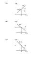
図3(a)は、一般的なNMOSトランジスタの「Vgs>Vth」領域のうちの飽和領域におけるIds-Vgs特性を示すグラフである。横軸は、ゲート-ソース電圧Vgs[V]を示し、縦軸は、ドレイン電流Ids[μA]を示す。 FIG. 3A is a graph showing the Ids-Vgs characteristics in the saturation region of the “Vgs> Vth” region of a general NaCl transistor. The horizontal axis represents the gate-source voltage Vgs [V], and the vertical axis represents the drain current Ids [μA].
図3(b)は、一般的なNMOSトランジスタのIds-Vds特性を示すグラフである。横軸は、ドレイン-ソース電圧Vds[V]を示し、縦軸は、ドレイン電流Ids[μA]を示す。図3(b)では、Vgs=0.8V、1.0V、1.2Vでのドレイン電流Idsが示される。 FIG. 3 (b) is a graph showing the Ids-Vds characteristics of a general NaCl transistor. The horizontal axis represents the drain-source voltage Vds [V], and the vertical axis represents the drain current Ids [μA]. FIG. 3B shows the drain currents Ids at Vgs = 0.8V, 1.0V, 1.2V.
「Vgs>Vth」領域のうち「Vds>Vgs-Vth」で示される領域がNMOSトランジスタの飽和領域である。飽和領域におけるドレイン電流Idsは、式(3)によって示される。式(3)において、Coxは、NMOSトランジスタのゲート容量を示し、μnは、NMOSトランジスタの電子移動度を示す。LはNMOSトランジスタのゲート長を示し、WはNMOSトランジスタのゲート幅を示す。 Of the "Vgs> Vth" regions, the region represented by "Vds> Vgs-Vth" is the saturation region of the NaCl transistor. The drain current Ids in the saturation region is represented by Eq. (3). In the formula (3), Cox indicates the gate capacitance of the HCl transistor, and μn indicates the electron mobility of the nanotube transistor. L indicates the gate length of the NaOH transistor, and W indicates the gate width of the Now's transistor.
図3(a)と図3(b)の「飽和領域」とに、式(3)による標準的な回路パラメータを使用したシミュレーション結果を示す。図3(a)に示すように、ゲート-ソース電圧Vgsが閾値電圧Vthより大きくなると、ドレイン電流Idsが流れる。そして、図3(b)に示すように、飽和領域では、ドレイン電流Idsがほぼ一定値に飽和する。つまり、飽和領域では、ドレイン電流Idsは、ドレイン-ソース電圧Vdsに依存しない。NMOSトランジスタにおいて基本的に使用される領域は、飽和領域である。 The simulation results using the standard circuit parameters according to the equation (3) are shown in the “saturation region” of FIGS. 3 (a) and 3 (b). As shown in FIG. 3A, when the gate-source voltage Vgs becomes larger than the threshold voltage Vth, the drain current Ids flows. Then, as shown in FIG. 3B, the drain current Ids is saturated to a substantially constant value in the saturation region. That is, in the saturation region, the drain current Ids does not depend on the drain-source voltage Vds. The region basically used in the NaCl transistor is the saturation region.

一方、「Vgs>Vth」領域のうち「Vds<Vgs-Vth」で示される領域がNMOSトランジスタの線形領域である。線形領域におけるドレイン電流Idsは、式(4)によって示される。図3(b)の「線形領域」に、式(4)による標準的な回路パラメータを使用したシミュレーション結果を示す。図3(b)に示すように、「線形領域」では、ドレイン-ソース電圧Vdsに対してドレイン電流Idsが線形的に変化する。 On the other hand, the region represented by "Vds <Vgs-Vth" in the "Vgs> Vth" region is the linear region of the µtransistor. The drain current Ids in the linear region is represented by Eq. (4). The "linear region" in FIG. 3B shows the simulation results using the standard circuit parameters according to the equation (4). As shown in FIG. 3B, in the “linear region”, the drain current Ids changes linearly with respect to the drain-source voltage Vds.

すなわち、線形領域においては、Ids-Vds特性を線形近似できるため、好ましい例として、NMOSトランジスタをMOS抵抗として利用し易い。具体的には、Vds=0での式(4)に基づく接線方程式から、ドレイン電流Idsは、式(5)に示すように線形近似できる。 That is, in the linear region, the Ids-Vds characteristic can be linearly approximated, and therefore, as a preferable example, the MIMO transistor can be easily used as the MOS resistance. Specifically, the drain current Ids can be linearly approximated as shown in the equation (5) from the tangent equation based on the equation (4) at Vds = 0.

式(5)から理解できるように、ゲート-ソース電圧Vgsによりドレイン電流Idsを制御できる。Vgsによってドレイン電流Idsを制御できることは、VgsによってNMOSトランジスタの抵抗値Rを制御できることと同義である。なぜなら、R=Vds/Idsだからである。図3(b)の破線で示す直線は、Vgs=0.8V、1.0V、1.2Vでの式(5)による標準的な回路パラメータを使用したシミュレーション結果を示す。Vgsが小さいほど、破線で示す直線の傾きが小さくなる。つまり、Vgsが小さいほど、抵抗値Rが上昇する。 As can be understood from the equation (5), the drain current Ids can be controlled by the gate-source voltage Vgs. The fact that the drain current Ids can be controlled by Vgs is synonymous with the fact that the resistance value R of the Now's transistor can be controlled by Vgs. This is because R = Vds / Ids. The straight line shown by the broken line in FIG. 3B shows the simulation result using the standard circuit parameter according to the equation (5) at Vgs = 0.8V, 1.0V, 1.2V. The smaller Vgs, the smaller the slope of the straight line shown by the broken line. That is, the smaller the Vgs, the higher the resistance value R.
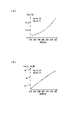
そこで、ゲート-ソース電圧Vgs[V]とドレイン電流Ids[nA]及び抵抗値R[MΩ]との関係を図4(a)及び図4(b)に示す。図4(a)及び図4(b)は、式(4)に基づく標準的な回路パラメータを使用したシミュレーション結果を示す。 Therefore, the relationship between the gate-source voltage Vgs [V], the drain current Ids [nA], and the resistance value R [MΩ] is shown in FIGS. 4 (a) and 4 (b). 4 (a) and 4 (b) show simulation results using standard circuit parameters based on equation (4).
図4(a)に示すように、一例として、ドレイン電流Idsは、数100mVの範囲でのゲート-ソース電圧Vgsの増加に応じて、線形に増加する。つまり、ドレイン電流Idsは、数100mVの範囲でのゲート-ソース電圧Vgsに比例する。 As shown in FIG. 4A, as an example, the drain current Ids increases linearly with increasing gate-source voltage Vgs in the range of several hundred mV. That is, the drain current Ids is proportional to the gate-source voltage Vgs in the range of several hundred mV.
MOS抵抗としてのNMOSトランジスタの抵抗値Rは、式(6)のように表せるため、図4(b)に示すように、抵抗値Rはゲート-ソース電圧Vgsに反比例する。 Since the resistance value R of the NaCl transistor as the MOS resistance can be expressed by the equation (6), the resistance value R is inversely proportional to the gate-source voltage Vgs as shown in FIG. 4 (b).
R=Vds/Ids …(6) R = Vds / Ids ... (6)
なお、図3(a)~図4(b)における標準的な回路パラメータによるシミュレーションの条件は、μn・Cox=170.0μA/V2、W=0.6μm、L=60.0μm、αth=-1.7mV/K、αμ=-1.5、Vth=0.7V、T0=300K、C=800.0fF、とした。The conditions for simulation using the standard circuit parameters in FIGS. 3 (a) to 4 (b) are μn · Cox = 170.0 μA / V 2 , W = 0.6 μm, L = 60.0 μm, αth =. -1.7 mV / K, αμ = -1.5, Vth = 0.7 V, T0 = 300K, C = 800.0 fF.
以上、図3(a)~図4(b)を参照して説明したように、NMOSトランジスタによるMOS抵抗は、「Vgs>Vth」領域のうちの線形領域において線形抵抗として使用でき、例えば、MOS抵抗に流れる電流はゲート-ソース電圧Vgsに比例するし、MOS抵抗で構成したRCフィルタの遮断周波数fcはゲート-ソース電圧Vgsに比例する。すなわち、MOS抵抗に流れる電流及びRCフィルタの遮断周波数fcをVgsにより線形的に制御できる。 As described above with reference to FIGS. 3 (a) to 4 (b), the MOS resistance by the NaCl transistor can be used as a linear resistance in the linear region in the “Vgs> Vth” region, for example, MOS. The current flowing through the resistor is proportional to the gate-source voltage Vgs, and the cutoff frequency fc of the RC filter composed of the MOS resistor is proportional to the gate-source voltage Vgs. That is, the current flowing through the MOS resistor and the cutoff frequency fc of the RC filter can be linearly controlled by Vgs.
但し、NMOSトランジスタの閾値電圧Vth及び電子移動度μnには温度依存性がある。温度依存性を考慮した閾値電圧Vthは、式(7)によって示される。ここで、αthは、閾値電圧Vthの温度係数を示す。Vth_T0は、温度T0での閾値電圧Vthを示す。つまり、式(7)のように、任意の温度T0で観測値として得られる閾値電圧Vth_T0を境に、温度のT0からの変化に応じて閾値電圧VthがVth_T0から変化する。 However, the threshold voltage Vth and the electron mobility μn of the nanotube transistor have a temperature dependence. The threshold voltage Vth considering the temperature dependence is represented by the equation (7). Here, αth indicates the temperature coefficient of the threshold voltage Vth. Vth_T0 indicates the threshold voltage Vth at the temperature T0. That is, as in the equation (7), the threshold voltage Vth changes from Vth_T0 according to the change from T0 of the temperature with the threshold voltage Vth_T0 obtained as an observed value at an arbitrary temperature T0 as a boundary.

温度依存性を考慮した電子移動度μnは、式(8)によって示される。ここで、αμは、電子移動度μnの温度係数を示す。μn_T0は、温度T0での電子移動度μnを示す。つまり、式(8)のように、任意の温度T0で観測値として得られる電子移動度はμn_T0を境に、温度のT0からの変化に応じて電子移動度μnがμn_T0から変化する。 The electron mobility μn considering the temperature dependence is represented by the equation (8). Here, αμ indicates the temperature coefficient of electron mobility μn. μn_T0 indicates the electron mobility μn at the temperature T0. That is, as shown in the equation (8), the electron mobility obtained as an observed value at an arbitrary temperature T0 changes from μn_T0 in accordance with the change in temperature from T0.

式(4)、式(7)、及び、式(8)に基づいて、NMOSトランジスタの線形領域において、閾値電圧Vthと電子移動度μnとの双方の温度依存性を反映したドレイン電流Idsは、式(9)によって示される。 Based on the equations (4), (7), and (8), the drain current Ids reflecting the temperature dependence of both the threshold voltage Vth and the electron mobility μn in the linear region of the NaCl transistor is determined. It is represented by the equation (9).

図5は、一般的なNMOSトランジスタの「Vgs>Vth」領域のうちの線形領域におけるドレイン電流Idsの温度依存性を示すグラフである。横軸は、温度[K]を示し、縦軸は、ドレイン電流Ids[nA]を示す。図5において、線500は、式(9)において、αμ=0として、閾値電圧Vthの温度依存性だけを反映させたときのドレイン電流Idsを示す。線501は、式(9)において、αth=0として、電子移動度μnの温度依存性だけを反映させたときのドレイン電流Idsを示す。線502は、電子移動度μnと閾値電圧Vthとの双方の温度依存性を反映させたときの式(9)によるドレイン電流Idsを示す。
FIG. 5 is a graph showing the temperature dependence of the drain current Ids in the linear region of the “Vgs> Vth” region of a typical NaCl transistor. The horizontal axis represents the temperature [K], and the vertical axis represents the drain current Ids [nA]. In FIG. 5, the
式(7)及び式(9)の閾値電圧Vthの温度係数αthは負の値をとるため、図5の線500で示されるように、閾値電圧Vthの温度依存性のみを考慮すると、ドレイン電流Idsは、温度上昇にともなって線形に増加する。定性的には、温度上昇にともない移動可能な荷電粒子数が増加することにより、閾値電圧Vthが低下するからである。
Since the temperature coefficient αth of the threshold voltage Vth in the equations (7) and (9) takes a negative value, as shown by
また、式(8)及び式(9)の電子移動度μnの温度係数αμは負の値をとるため、図5の線501で示されるように、電子移動度μnの温度依存性のみを考慮すると、ドレイン電流Idsは、温度上昇にともなって概ね線形に減少する。定性的には、温度が上昇するとシリコン結晶格子の熱振動により荷電粒子の移動が阻害されるためである。
Further, since the temperature coefficient αμ of the electron mobility μn in the equations (8) and (9) takes a negative value, only the temperature dependence of the electron mobility μn is considered as shown by the
すなわち、線500及び線501で示されるように、閾値電圧Vthの温度依存性を反映したドレイン電流Ids、及び、電子移動度μnの温度依存性反映したドレイン電流Idsは、線形近似できる。
That is, as shown by the
従って、線502で示されるように、閾値電圧Vthの温度依存性と電子移動度μnの温度依存性との双方を反映したドレイン電流Idsもまた、線形近似できる。
Therefore, as shown by
具体的には、線502で示されるように、ドレイン電流Idsは、温度上昇にともなって概ね線形に増加する。この理由は、閾値電圧Vthの温度依存性の方が、電子移動度μnの温度依存性よりも、ドレイン電流Idsに及ぼす影響が大きいからである。換言すれば、閾値電圧Vthの温度依存性の影響が、電子移動度μnの温度依存性の影響により抑制される。
Specifically, as shown by
一例として、標準的な閾値電圧Vthの温度係数αthは、-1.7mV/Kであるので、50度の温度上昇によって、閾値電圧Vthが85mV低下する。さらに、閾値電圧Vthの低下幅(85mV)は、電子移動度μnの温度依存性による抑制効果によって狭くなる(85mV未満)。 As an example, the temperature coefficient αth of the standard threshold voltage Vth is -1.7 mV / K, so that the temperature rise of 50 degrees lowers the threshold voltage Vth by 85 mV. Further, the decrease width (85 mV) of the threshold voltage Vth is narrowed (less than 85 mV) due to the suppression effect due to the temperature dependence of the electron mobility μn.
一方、図4(a)に示すように、一例として、ゲート-ソース電圧Vgsを100mV上昇させたときのドレイン電流Idsの増加量は、線形近似できる。 On the other hand, as shown in FIG. 4A, as an example, the amount of increase in the drain current Ids when the gate-source voltage Vgs is increased by 100 mV can be linearly approximated.
従って、温度上昇に伴って線形に増加するドレイン電流Ids(図5の線502)に応じてゲート-ソース電圧Vgsを線形に下げて、ドレイン電流Idsを線形に減少させることで、ドレイン電流Idsの温度依存性を抑制できる。その結果、「Vgs>Vth」領域のうちの線形領域において、MOS抵抗としてのNMOSトランジスタの温度依存性を補正できる。
Therefore, the drain current Ids is reduced by linearly lowering the gate-source voltage Vgs in response to the drain current Ids (
以上より、「Vgs>Vth」領域のうちの線形領域において、トランジスタTNのゲート-ソース間に印加する式(1)に示す制御電圧Vgsのように、基準電圧Vgs0に式(2)に示す温度Tに応じて線形に変化する補正電圧Vcを加算することで、MOS抵抗MRとしてのトランジスタTNの温度依存性を補正できることが分かる。 From the above, in the linear region of the "Vgs> Vth" region, the temperature shown in the equation (2) is set to the reference voltage Vgs0 like the control voltage Vgs shown in the equation (1) applied between the gate and the source of the transistor TN. It can be seen that the temperature dependence of the transistor TN as the MOS resistance MR can be corrected by adding the correction voltage Vc that changes linearly according to T.
同様に、トランジスタTNの「Vgs>Vth」領域のうちの飽和領域でも、式(1)に示す制御電圧Vgsのように、基準電圧Vgs0に式(2)に示す温度Tに応じて線形に変化する補正電圧Vcを加算することで、MOS抵抗としてのトランジスタTNの温度依存性を補正できる。この点を、図6(a)及び図6(b)を参照して説明する。 Similarly, even in the saturation region of the “Vgs> Vth” region of the transistor TN, the reference voltage Vgs0 changes linearly according to the temperature T shown in the equation (2), as in the control voltage Vgs shown in the equation (1). By adding the correction voltage Vc to be applied, the temperature dependence of the transistor TN as the MOS resistance can be corrected. This point will be described with reference to FIGS. 6 (a) and 6 (b).
図6(a)は、式(3)による一般的なNMOSトランジスタの「Vgs>Vth」領域のうちの飽和領域におけるゲート-ソース電圧Vgsに対するドレイン電流Idsを示したグラフである。図6(a)に示すように、ドレイン電流Idsは、図4(a)の線形領域に比べると、非線形性があるものの100mV程度の範囲においては線形近似可能である。 FIG. 6 (a) is a graph showing the drain current Ids with respect to the gate-source voltage Vgs in the saturation region in the “Vgs> Vth” region of a general NaCl transistor according to the equation (3). As shown in FIG. 6A, the drain current Ids can be linearly approximated in a range of about 100 mV, although there is a non-linearity as compared with the linear region of FIG. 4A.
一方、温度依存性を反映したNMOSトランジスタの飽和領域におけるドレイン電流Idsは、式(3)、式(7)、及び、式(8)に基づいて、式(10)によって示される。 On the other hand, the drain current Ids in the saturation region of the nanotube transistor reflecting the temperature dependence is represented by the equation (10) based on the equations (3), (7), and (8).

図6(b)は、一般的なNMOSトランジスタの「Vgs>Vth」領域のうちの飽和領域におけるドレイン電流Idsの温度依存性を示すグラフである。横軸は、温度[K]を示し、縦軸は、ドレイン電流Ids[nA]を示す。図6(b)において、線503は、式(10)において、αμ=0として、閾値電圧Vthの温度依存性だけを反映させたときのドレイン電流Idsを示す。線504は、式(10)において、αth=0として、電子移動度μnの温度依存性だけを反映させたときのドレイン電流Idsを示す。線505は、電子移動度μnと閾値電圧Vthとの双方の温度依存性を反映させたときの式(10)によるドレイン電流Idsを示す。
FIG. 6 (b) is a graph showing the temperature dependence of the drain current Ids in the saturation region of the “Vgs> Vth” region of a general NaCl transistor. The horizontal axis represents the temperature [K], and the vertical axis represents the drain current Ids [nA]. In FIG. 6B, the
線505で示されるように、「Vgs>Vth」領域のうちの飽和領域においても線形領域と同様に、閾値電圧Vthの温度依存性と電子移動度μnの温度依存性との双方を反映したドレイン電流Idsもまた、線形近似できる。一例として、標準的な閾値電圧Vthの温度係数αthは、-1.7mV/Kであり、電子移動度μnの温度依存性による抑制効果があることにより、飽和領域においても線形領域と同様に、50度の温度上昇にともなう閾値電圧Vthの低下幅は、85mV未満である。一方、図6(a)に示すように、一例として、ゲート-ソース電圧Vgsを100mV上昇させたときのドレイン電流Idsの増加量は、線形近似できる。
As shown by
従って、温度上昇に伴って線形に増加するドレイン電流Ids(図6(b)の線505)に応じてゲート-ソース電圧Vgsを線形に下げて、ドレイン電流Idsを線形に減少させることで、ドレイン電流Idsの温度依存性を抑制できる。その結果、「Vgs>Vth」領域のうちの飽和領域において、MOS抵抗としてのNMOSトランジスタの温度依存性を補正できる。
Therefore, by linearly lowering the gate-source voltage Vgs in response to the drain current Ids (
以上より、「Vgs>Vth」領域のうちの飽和領域においても、トランジスタTNのゲート-ソース間に印加する式(1)に示す制御電圧Vgsのように、基準電圧Vgs0に式(2)に示す温度Tに応じて線形に変化する補正電圧Vcを加算することで、MOS抵抗MRとしてのトランジスタTNの温度依存性を補正できることが分かる。 From the above, even in the saturation region of the “Vgs> Vth” region, the reference voltage Vgs0 is shown in the equation (2) like the control voltage Vgs shown in the equation (1) applied between the gate and the source of the transistor TN. It can be seen that the temperature dependence of the transistor TN as the MOS resistance MR can be corrected by adding the correction voltage Vc that changes linearly according to the temperature T.
なお、図5~図6(b)における標準的な回路パラメータによるシミュレーションの条件は、μn_T0・Cox=170.0μA/V2、W=0.6μm、L=60.0μm、αth=-1.7mV/K、αμ=-1.5、Vth_T0=0.7V、T0=300K、C=800.0fF、とした。The conditions for simulation using the standard circuit parameters in FIGS. 5 to 6 (b) are μn_T0 · Cox = 170.0 μA / V 2 , W = 0.6 μm, L = 60.0 μm, αth = -1. It was set to 7 mV / K, αμ = −1.5, Vth_T0 = 0.7V, T0 = 300K, and C = 800.0 fF.
以上、図3(a)~図6(b)を参照して説明したように、線形領域、及び、飽和領域に関わらず、ゲート-ソース電圧Vgsが閾値電圧Vthより大きい「Vgs>Vth」領域において、トランジスタTNのゲート-ソース間に印加する式(1)に示す制御電圧Vgsのように、基準電圧Vgs0に式(2)に示す温度Tに応じて線形に変化する補正電圧Vcを加算することで、MOS抵抗MRとしてのトランジスタTNの温度依存性を補正できる。 As described above with reference to FIGS. 3 (a) to 6 (b), the “Vgs> Vth” region in which the gate-source voltage Vgs is larger than the threshold voltage Vth regardless of the linear region and the saturation region. In, a correction voltage Vc that changes linearly according to the temperature T shown in the equation (2) is added to the reference voltage Vgs0 like the control voltage Vgs shown in the equation (1) applied between the gate and the source of the transistor TN. Therefore, the temperature dependence of the transistor TN as the MOS resistance MR can be corrected.
式(1)及び式(2)に基づく手法に従って、トランジスタTNで構成されるMOS抵抗MRの温度依存性を補正する回路の一例が、図1の電圧印加回路1である。再び図1を参照して、電圧印加回路1の詳細を説明する。電圧印加回路1は、トランジスタTNのゲート端子とソース端子との間に配置される。ソース端子の電位(以下、「ソース電位Vs」と記載する場合がある)は、任意の値を取り得る。具体的には、トランジスタTNのドレイン端子及びソース端子の2端子は、MOS抵抗MRの両端の2端子として使用されるため、アース又はグラウンド(0[V])とは電気的に独立した状態(例えば浮いた状態)で使用される。その結果、ソース電位Vsは、任意の値を取り得る。
An example of a circuit that corrects the temperature dependence of the MOS resistance MR composed of the transistor TN according to the method based on the equations (1) and (2) is the
電圧印加回路1は、制御電圧印加部9と、温度検出部13とを含む。温度検出部13は、温度Tを検出して、温度Tに応じた検出信号TMを制御電圧印加部9に出力する。温度検出部13が、温度Tを検出して、温度Tを示す物理量(例えば、電流又は電圧)を表す検出信号TM、又は、温度Tに相関のある物理量(例えば、電流又は電圧)を表す検出信号TMを出力できる限りは、温度検出部13の構成は、特に限定されない。例えば、温度検出部13は、サーミスタのような温度センサーを含んでいてもよい。例えば、温度検出部13は、電界効果トランジスタ又はバイポーラトランジスタを含んでいて、電界効果トランジスタ又はバイポーラトランジスタの温度依存特性を利用してもよい。例えば、温度検出部13は、PTAT(Proportional To Absolute Temperature)回路を含んでいてもよい。PTAT回路は、絶対温度に比例する電流を検出信号TMとして出力する。例えば、温度検出部13は、温度Tを検出して、検出信号TMを出力する温度検出回路によって構成される。
The
制御電圧印加部9は、温度Tを示す検出信号TMに応じた制御電圧VgsをトランジスタTNのゲート-ソース間に印加する。具体的には、制御電圧印加部9は、検出信号TMに応じて温度Tに対して線形に変化する補正電圧Vcを制御電圧Vgsが含むように、制御電圧Vgsを生成する。そして、制御電圧印加部9は、制御電圧VgsをトランジスタTNのゲート-ソース間に印加する。従って、実施形態1によれば、温度Tを示す検出信号TMに応じて適切に、トランジスタTNの抵抗値Rの温度依存性を低減できる。
The control
具体的には、制御電圧印加部9は、制御電圧生成部10と、電圧制御電圧源19とを含む。さらに、制御電圧生成部10は、基準電圧生成部11と、補正電圧生成部15と、加算部17とを含む。基準電圧生成部11は、式(1)における基準電圧Vgs0を生成して、基準電圧Vgs0を加算部17に出力する。補正電圧生成部15は、温度Tに対して線形に変化する補正電圧Vcを温度の検出信号TMに基づいて生成して、補正電圧Vcを加算部17に出力する。加算部17は、基準電圧Vgs0と補正電圧Vcとを加算し、加算結果である制御電圧Vgsaを生成する。このようにして、制御電圧生成部10は制御電圧Vgsaを生成する。制御電圧Vgsaを「基準制御電圧Vgsa」と記載してもよい。制御電圧Vgsaは、式(11)によって示される。
Specifically, the control
Vgsa=Vgs0+Vc …(11) Vgsa = Vgs0 + Vc ... (11)
式(1)及び式(11)から明らかなように、制御電圧Vgsaと制御電圧Vgsとは、同じ電圧成分(基準電圧Vgs0及び補正電圧Vc)及び同じ電圧値を有している。式(11)においても、補正電圧Vcは式(2)によって示される。式(2)に示す補正電圧Vcは、図2に示すように、温度Tに上昇に従い、線形に減少する。すなわち、トランジスタTNの場合、補正係数βは負の値をとる。そして、補正係数βを変更することで、温度Tに応じて制御電圧Vgsaを下げる割合を調整することができる。 As is clear from the equations (1) and (11), the control voltage Vgsa and the control voltage Vgs have the same voltage component (reference voltage Vgs0 and correction voltage Vc) and the same voltage value. Also in the equation (11), the correction voltage Vc is represented by the equation (2). As shown in FIG. 2, the correction voltage Vc shown in the equation (2) decreases linearly as the temperature T increases. That is, in the case of the transistor TN, the correction coefficient β takes a negative value. Then, by changing the correction coefficient β, the ratio of lowering the control voltage Vgsa can be adjusted according to the temperature T.
ここで、制御電圧Vgsaは、具体的には、0[V]を基準とする電圧(つまり、0[V]を基準とする電位差)である。一方、トランジスタTNのソース電位Vsは、任意の値を取り得る。したがって、制御電圧Vgsaをゲート-ソース間に直接印加すると、トランジスタTNのソース電位Vsがアース又はグラウンド(0[V])から独立に任意の値をとる場合に、「Vgsa-Vs」がトランジスタTNのゲート-ソース間の電圧になる。その結果、ソース電位Vsに応じて、トランジスタTNの抵抗値Rが変化し得る。そこで、実施形態1では、制御電圧Vgsaが間接的にトランジスタTNのゲート-ソース間に印加される。この場合の好ましい例として、実施形態1では、制御電圧印加部9が電圧制御電圧源19を有している。ただし、例えば、トランジスタTNのソース電位Vsが一定値をとる場合、及び/又は、ソース電位Vsの変動に伴う抵抗値Rの変化が許容できる場合は、トランジスタTNのゲート-ソース間に、制御電圧Vgsaを直接印加してもよい。
Here, the control voltage Vgsa is specifically a voltage based on 0 [V] (that is, a potential difference based on 0 [V]). On the other hand, the source potential Vs of the transistor TN can take any value. Therefore, when the control voltage Vgsa is applied directly between the gate and the source, "Vgsa-Vs" becomes the transistor TN when the source potential Vs of the transistor TN takes an arbitrary value independently of the ground or ground (0 [V]). It becomes the voltage between the gate and the source of. As a result, the resistance value R of the transistor TN may change according to the source potential Vs. Therefore, in the first embodiment, the control voltage Vgsa is indirectly applied between the gate and the source of the transistor TN. As a preferred example in this case, in the first embodiment, the control
電圧制御電圧源19は、トランジスタTNのゲート端子とソース端子との間に接続される。電圧制御電圧源19は、入力のための2端子と、出力のための2端子とを有する。そして、電圧制御電圧源19は、入力の2端子間の電位差に応じて、出力の2端子間の電位差が決まる電圧源である。電圧制御電圧源19には、制御電圧生成部10から、0[V]を基準とする制御電圧Vgsaと、基準となる電圧0[V]が入力されることで、制御電圧Vgsaが電位差として入力される。そして、電圧制御電圧源19の出力の2端子をそれぞれトランジスタTNのゲート端子及びソース端子に接続することで、トランジスタTNのゲート-ソース間に制御電圧Vgsaと同じ電圧値を有する制御電圧Vgsが印加される。このとき、ソース電位Vsが変動しても、電圧制御電圧源19の出力の2端子間の電位差、つまり、制御電圧Vgsは変動しない。
Voltage control The
また、電圧制御電圧源19には、制御電圧Vgsaが電位差として入力されればよいので、基準となる電圧0[V]を任意の値にしてもよい。この場合、基準となる電圧をVrefとすると、制御電圧生成部10からの出力電圧を「Vgsa+Vref」とすれば、電圧制御電圧源19に入力される電位差は、「Vgsa+Vref-Vref」によりVgsaとなる。
Further, since the control voltage Vgsa may be input to the voltage
以上より、図1の電圧印加回路1が式(1)に示される任意の制御電圧VgsをトランジスタTNのゲート-ソース間に印加することができる。具体的には、トランジスタTNで構成されるMOS抵抗MRのドレイン電流Idsが温度Tの上昇に伴って略線形に増加することに対して(図5の線502、図6(b)の線505)、電圧印加回路1において補正電圧Vc(図2)の補正係数βを適切に設定することで、電圧印加回路1は、温度Tに応じて制御電圧Vgsを線形に下げて、ドレイン電流Idsを線形に減少させる。その結果、ドレイン電流Idsの温度依存性を抑制できる。ドレイン電流Idsの温度依存性を抑制できると、トランジスタTNに関する物理量の温度依存性を抑制できる。
From the above, the
具体的な回路について、まず電圧制御電圧源19の一例を図7(a)及び図7(b)を参照して、説明する。図7(a)は、電圧制御電圧源19の第1例を示す回路図である。図7(a)に示すように、第1例に係る電圧制御電圧源19は、第1スイッチ回路191と、第2スイッチ回路192と、キャパシタ193とを含む。
A specific circuit will be described first with reference to FIGS. 7 (a) and 7 (b) as an example of the voltage
第1スイッチ回路191は、端子t1~端子t3を含む。端子t1は制御電圧生成部10に接続される。端子t2はトランジスタTNのゲート端子に接続される。端子t3は、キャパシタ193の一方端子に接続される。
The
第2スイッチ回路192は、端子t4~端子t6を含む。端子t4は制御電圧生成部10に接続される。端子t5はトランジスタTNのソース端子に接続される。端子t6は、キャパシタ193の他方端子に接続される。
The
制御電圧生成部10が制御電圧Vgsaを生成する。第1スイッチ回路191は端子t3と端子t1とを接続する。加えて、第2スイッチ回路192は端子t6と端子t4とを接続する。その結果、キャパシタ193は制御電圧Vgsaを保持する。その後、第1スイッチ回路191は端子t3と端子t2とを接続する。加えて、第2スイッチ回路192は端子t6と端子t5とを接続する。その結果、キャパシタ193に保持された制御電圧Vgsaが制御電圧Vgsとして、トランジスタTNのゲート-ソース間に印加される。
The control
図7(b)は、電圧制御電圧源19の第2例を示す回路図である。図7(b)に示すように、第2例に係る電圧制御電圧源19は、第1例に係る電圧制御電圧源19の構成に加えて、オペアンプ194をさらに含む。以下、第2例が第1例と異なる点を主に説明する。
FIG. 7B is a circuit diagram showing a second example of the voltage
第2例では、オペアンプ194の出力端子がノードNに接続される。ノードNは、端子t2とトランジスタTNのゲート端子とを接続するラインに位置する。オペアンプ194の反転入力端子が端子t5に接続される。オペアンプ194の非反転入力端子がトランジスタTNのソース端子に接続される。オペアンプ194が図7(b)のように帰還回路を形成している場合、非反転入力端子と反転入力端子の電位はほぼ等しくなる(仮想短絡)。従って、反転入力端子の電位はトランジスタTNのソース電位Vsと等しくなる。その結果、キャパシタ193に制御電圧Vgsaが保持されて、キャパシタ193がオペアンプ194に接続されると、オペアンプ194の出力端子であるノードNの電位は「Vgsa+Vs」となる。よって、トランジスタTNのゲート-ソース電圧Vgsは制御電圧Vgsaとほぼ等しくなる。
In the second example, the output terminal of the
すなわち、第2例に係る電圧制御電圧源19の動作は、第1例に係る電圧制御電圧源19の動作と同様である。特に、第2例では、トランジスタTNのソース端子がオペアンプ194の非反転入力端子に接続されるため、第1例と比較して、トランジスタTNのゲート端子及びソース端子の容量負荷の影響を低減できる。
That is, the operation of the voltage
なお、電圧制御電圧源19が電気的に浮いている任意の2端子間に挿入可能な限りにおいては、電圧制御電圧源19の構成は特に限定されない。
The configuration of the voltage
制御電圧生成部10の構成については、式(11)によって表される制御電圧Vgsaを生成できる限りは、特に限定されず、任意の制御電圧生成回路によって構成できる。
The configuration of the control
なお、図1では、制御電圧生成部10の物理的又は論理的構成が示される。従って、図1が制御電圧生成部10の物理的構成を表す場合には、例えば、基準電圧生成部11は、基準電圧Vgs0を生成する基準電圧生成回路によって構成され、補正電圧生成部15は、温度検出部13の検出信号TMに基づいて補正電圧Vcを生成する補正電圧生成回路によって構成され、加算部17は、基準電圧Vgs0に補正電圧Vcを加算する加算回路によって構成される。
Note that FIG. 1 shows the physical or logical configuration of the control
また、図1が制御電圧生成部10の論理的構成を表す場合には、例えば、基準電圧生成部11と補正電圧生成部15と加算部17とが物理的構成として明確に区別されていない場合であっても、制御電圧生成部10が式(11)で示される制御電圧Vgsaを生成する限りは、制御電圧生成部10を構成する回路は特に限定されない。
Further, when FIG. 1 represents the logical configuration of the control
さらに、温度検出部13及び補正電圧生成部15の構成についても、図1では、温度検出部13及び補正電圧生成部15の物理的又は論理的構成が示されている。従って、温度検出部13及び補正電圧生成部15が論理的構成を表す場合には、例えば、温度検出部13と補正電圧生成部15とが物理的構成として明確に区別されていない場合であっても、式(2)によって表される補正電圧Vcを生成できる限りは、特に限定されず、任意の温度検出回路及び補正電圧生成回路によって構成できる。
Further, regarding the configuration of the
温度検出部13及び補正電圧生成部15の一例を、図8を参照して説明する。図8は、温度検出部13及び補正電圧生成部15の一例を示す回路図である。温度検出部13及び補正電圧生成部15は、第1電流源回路131、第2電流源回路133、及び可変抵抗Roを含む。第1電流源回路131と第2電流源回路133とは、第1電源ラインPL1と第2電源ラインPL2との間に直列に接続される。第1電流源回路131と第2電流源回路133との間のノードNcに可変抵抗Roの一方端子が接続される。可変抵抗Roの他方端子は接地される。この場合、第1電源ラインPL1の電位は正の値をとり、例えば、第1電源ラインPL1は、正電源電圧を供給する正電源に接続される。一方、第2電源ラインPL2の電位は負の値をとり、例えば、第2電源ラインPL2は、負電源電圧を供給する負電源に接続される。
An example of the
第1電流源回路131は第1電流Ipを生成する。第2電流源回路133は第2電流Imを生成する。可変抵抗Roには差分電流Ioが流れる。差分電流Ioは第1電流Ipと第2電流Imとの差分を示す電流である。具体的には、差分電流Ioは、第1電流Ipから第2電流Imを差し引いた電流である(Io=Ip-Im)。差分電流Ioが可変抵抗Roに流れることで、可変抵抗Roの両端間に電位差Vcが発生する。電位差Vcは、抵抗値Roに電流値Ioを乗じた値である(Vc=Ro×Io)。
The first
図8の回路では、温度検出部13と補正電圧生成部15とを明確に区別していないが、温度検出に第1電流源回路131と第2電流源回路133との温度依存性を用いる。第1電流Ip及び第2電流Imの温度依存性を示すグラフを図9(a)に示す。横軸は温度T[K]、縦軸は各電流源回路の電流値I[A]である。図9(a)に示すように、第1電流Ip及び第2電流Imの各々は、温度Tの変化に対して線形に変化する。そして、第1電流Ipの温度依存性と第2電流Imの温度依存性とは異なっている。つまり、温度検出部13の第1電流源回路131の温度依存性と第2電流源回路133の温度依存性とは異なっている。
In the circuit of FIG. 8, the
図9(a)の例では、第1電流Ipの温度依存性は第2電流Imの温度依存性よりも低い。つまり、第1電流源回路131の温度依存性は、第2電流源回路133の温度依存性よりも低い。このとき、可変抵抗Roに流れる差分電流Io(=Ip-Im)の温度依存性を図9(b)に示す。横軸は温度T[K]、縦軸は差分電流値Io[A]である。図9(b)に示すように、差分電流Ioは、負の温度特性を有する。つまり、差分電流Ioを表す直線の傾きAは負の値を有する。また、図9(a)において、第1電流Ipと第2電流Imとが一致するときの温度Tが第1温度T1である。第1温度T1のとき、差分電流Ioは図9(b)に示すようにゼロになる。従って、差分電流Ioは、式(12)によって表される。ここで、直列に接続された第1電流源回路131及び第2電流源回路133が、図1における温度検出部13を構成すると考えてもよい。また、差分電流Ioを、図1における温度検出部13の検出信号TMと考えてもよい。
In the example of FIG. 9A, the temperature dependence of the first current Ip is lower than the temperature dependence of the second current Im. That is, the temperature dependence of the first
Io=A×(T-T1) …(12) Io = A × (T-T1) ... (12)
差分電流Ioが可変抵抗Roに入力されたときの補正電圧Vcは、式(13)によって表される。補正電圧Vcの温度依存性を示すグラフを図9(c)に示す。横軸は温度T[K]、縦軸は補正電圧Vc[V]である。差分電流Ioが負の温度特性を有するため、図9(c)に示すように、補正電圧Vcも負の温度特性を有する。すなわち、図2に示す補正電圧Vcの温度依存性のグラフと一致する。また、温度が第1温度T1のとき、補正電圧Vcは図9(c)に示すようにゼロになる。ここで、補正係数βは、式(13)に示すように「Ro×A」であり、式(12)の傾きAと同様に負の値をとる。そして、補正係数βを変更したい場合は、可変抵抗Roを変更すればよいことが分かる。可変抵抗Roを、図1における補正電圧生成部15と考えてもよい。また、式(13)から明らかなように、補正電圧Vcは、差分電流Ioに基づく値を有する。
The correction voltage Vc when the differential current Io is input to the variable resistor Ro is expressed by the equation (13). A graph showing the temperature dependence of the correction voltage Vc is shown in FIG. 9 (c). The horizontal axis is the temperature T [K], and the vertical axis is the correction voltage Vc [V]. Since the differential current Io has a negative temperature characteristic, as shown in FIG. 9C, the correction voltage Vc also has a negative temperature characteristic. That is, it agrees with the graph of the temperature dependence of the correction voltage Vc shown in FIG. Further, when the temperature is the first temperature T1, the correction voltage Vc becomes zero as shown in FIG. 9 (c). Here, the correction coefficient β is “Ro × A” as shown in the equation (13), and takes a negative value like the slope A in the equation (12). Then, when it is desired to change the correction coefficient β, it can be seen that the variable resistor Ro should be changed. The variable resistor Ro may be considered as the correction
Vc=Ro×Io=Ro×A×(T-T1)=β(T-T1)
…(13)Vc = Ro × Io = Ro × A × (T-T1) = β (T-T1)
… (13)
ここで、差分電流Io及び補正電圧Vcがゼロになる第1温度T1は以下の方法により変更可能である。図8及び図10(a)~図10(c)を参照して、式(2)、式(12)及び式(13)に示す第1温度T1の変更方法を説明する。 Here, the first temperature T1 at which the differential current Io and the correction voltage Vc become zero can be changed by the following method. A method of changing the first temperature T1 shown in the formulas (2), (12) and (13) will be described with reference to FIGS. 8 and 10 (a) to 10 (c).
第1電流Ipの電流値を変更したときの第1電流Ip及び第2電流Imの温度依存性を示すグラフを図10(a)に示す。図10(a)に示すように、第1電流Ipと第2電流Imとが等しくなる温度が第1温度T1である。従って、第1電流Ipの電流値が増加すると、第1温度T1も増加する。すなわち、第1電流源回路131が第1電流Ipの電流値を変更することで、第1温度T1を変更することができる。
FIG. 10A shows a graph showing the temperature dependence of the first current Ip and the second current Im when the current value of the first current Ip is changed. As shown in FIG. 10A, the temperature at which the first current Ip and the second current Im are equal is the first temperature T1. Therefore, as the current value of the first current Ip increases, the first temperature T1 also increases. That is, the first
第2電流源回路133が第2電流Imの電流値を変更することでも、第1温度T1を変更することができる。図10(b)に、第2電流Imの電流値を変更したときの第1電流Ip及び第2電流Imの温度依存性を示すグラフを示す。ただし、図10(b)に示すように、第2電流Imの電流値が増加すると、第1温度T1は減少する。
The first temperature T1 can also be changed by the second
第1電流Ip及び/又は第2電流Imの電流値を変更すると、差分電流Ioの温度依存性も電流値に応じて変化する。図10(c)に、差分電流Ioの電流値が変更されたときの差分電流Ioの温度依存性を示すグラフを示す。図10(c)に示すように、第1電流Ip及び/又は第2電流Imの電流値の変更に伴い、差分電流Ioの電流値が増加すると、差分電流Ioがゼロになる温度Tである第1温度T1も増加する。また、差分電流Ioがゼロのとき、補正電圧Vcもゼロになる。 When the current values of the first current Ip and / or the second current Im are changed, the temperature dependence of the differential current Io also changes according to the current value. FIG. 10C shows a graph showing the temperature dependence of the differential current Io when the current value of the differential current Io is changed. As shown in FIG. 10 (c), it is a temperature T at which the differential current Io becomes zero when the current value of the differential current Io increases with the change of the current values of the first current Ip and / or the second current Im. The first temperature T1 also increases. Further, when the differential current Io is zero, the correction voltage Vc is also zero.
すなわち、実施形態1における図8の回路例においては、第1電流源回路131及び第2電流源回路133を設けて、第1電流Ip及び/又は第2電流Imを変更し、差分電流Ioを変更することで、補正電圧Vcがゼロになるときの温度Tである第1温度T1を容易に変更できる。
That is, in the circuit example of FIG. 8 in the first embodiment, the first
なお、第2電源ラインPL2が接地されていてもよい。この場合、可変抵抗Roの一方端子がノードNcに接続され、可変抵抗Roの他方端子が、参照電圧Vref(0<Vref<PL1電位)を生成する参照電圧源に接続される。このとき、補正電圧生成部15の出力電圧は、「β(T-T1)+Vref」になる。そこで、基準電圧生成部11の出力電圧を「Vgs0-Vref」に設定することで、式(11)と変わらず、Vgsa=Vgs0+β(T-T1)となる。
The second power supply line PL2 may be grounded. In this case, one terminal of the variable resistor Ro is connected to the node Nc, and the other terminal of the variable resistor Ro is connected to a reference voltage source that generates a reference voltage Vref (0 <Vref <PL1 potential). At this time, the output voltage of the correction
また、図9(a)及び図10の例では、第1電流Ip及び第2電流Imを表す直線の傾きは両者とも正の値であるが、必ずしも正の値である必要は無い。実施形態1において、トランジスタTNの温度依存性を補正するために補正電圧Vcの補正係数βが負となるためには、第2電流Imの傾きが第1電流Ipの傾きに比べて大きければよく、傾きの符号の正負は関係ない。 Further, in the examples of FIGS. 9A and 10A, the slopes of the straight lines representing the first current Ip and the second current Im are both positive values, but they do not necessarily have to be positive values. In the first embodiment, in order for the correction coefficient β of the correction voltage Vc to be negative in order to correct the temperature dependence of the transistor TN, it is sufficient that the slope of the second current Im is larger than the slope of the first current Ip. , The sign of the slope is irrelevant.
以上、図1に示す実施形態1に係る抵抗デバイス100の構成により、トランジスタTNの温度依存性を補正電圧Vcの補正係数βを適切に設定することで補正可能であることを説明した。この構成に従い、式(9)に式(1)及び式(2)を代入することで、「Vgs>Vth」領域のうちの線形領域(Vds<Vgs-Vth)において、トランジスタTNのドレイン電流Idsは、補正係数βを反映した式(14)によって表される。
It has been described above that the temperature dependence of the transistor TN can be corrected by appropriately setting the correction coefficient β of the correction voltage Vc by the configuration of the

また、式(10)に式(1)及び式(2)を代入することで、「Vgs>Vth」領域のうちの飽和領域(Vds>Vgs-Vth)において、トランジスタTNのドレイン電流Idsは、補正係数βを反映した式(15)によって表される。 Further, by substituting the equations (1) and (2) into the equation (10), the drain current Ids of the transistor TN can be changed in the saturation region (Vds> Vgs-Vth) in the “Vgs> Vth” region. It is expressed by the equation (15) reflecting the correction coefficient β.

式(14)及び式(15)には、温度Tに対して線形に変化する補正要素、つまり、補正電圧Vc(=β(T-T1))が含まれている。また、「Vgs>Vth」領域のうちの線形領域及び飽和領域のいずれにおいても、トランジスタTNの抵抗値Rは、式(16)によって示される。 Equations (14) and (15) include a correction element that changes linearly with respect to the temperature T, that is, a correction voltage Vc (= β (T—T1)). Further, the resistance value R of the transistor TN is represented by the equation (16) in both the linear region and the saturation region in the “Vgs> Vth” region.
R=Vds/Ids …(16) R = Vds / Ids ... (16)
補正係数βを適切に設定することで、トランジスタTNのドレイン電流Idsの温度依存性がなくなる。換言すれば、補正係数βを適切に設定することで、ドレイン電流Idsに基づく抵抗値R(式(16))の温度依存性がなくなる。図11(a)を参照して、補正電圧Vcを定める補正係数βの決定方法の一例を説明する。この例では、トランジスタTNの飽和領域に着目する。 By appropriately setting the correction coefficient β, the temperature dependence of the drain current Ids of the transistor TN is eliminated. In other words, by appropriately setting the correction coefficient β, the temperature dependence of the resistance value R (Equation (16)) based on the drain current Ids is eliminated. An example of a method for determining the correction coefficient β that determines the correction voltage Vc will be described with reference to FIG. 11A. In this example, we focus on the saturation region of the transistor TN.
図11(a)は、複数の異なる温度において、補正係数βとトランジスタTNの抵抗値Rとの関係を示すグラフである。横軸は補正係数βを示し、縦軸は抵抗値R[MΩ]を示す。 FIG. 11A is a graph showing the relationship between the correction coefficient β and the resistance value R of the transistor TN at a plurality of different temperatures. The horizontal axis shows the correction coefficient β, and the vertical axis shows the resistance value R [MΩ].
図11(a)に示すように、「Vgs>Vth」領域のうちの飽和領域における式(15)及び式(16)に基づいて抵抗値Rをシミュレーションして、R-β曲線G10~G16が得られた。標準的な回路パラメータによるシミュレーションの条件は、μn_T0・Cox=170.0μA/V2、W=0.6μm、L=60.0μm、αth=-1.7mV/K、αμ=-1.5、Vth_T0=0.7V、T0=300K、T1=320K、である。また、基準電圧Vgs0は、0.9Vであり、ドレイン-ソース電圧Vdsは、1.8Vである。As shown in FIG. 11A, the resistance value R is simulated based on the equations (15) and (16) in the saturated region in the “Vgs> Vth” region, and the R-β curves G10 to G16 are obtained. Obtained. Simulation conditions with standard circuit parameters are μn_T0 · Cox = 170.0 μA / V 2 , W = 0.6 μm, L = 60.0 μm, αth = -1.7 mV / K, αμ = -1.5, Vth_T0 = 0.7V, T0 = 300K, T1 = 320K. The reference voltage Vgs0 is 0.9V, and the drain-source voltage Vds is 1.8V.
R-β曲線G10、G11、G12、G13、G14、G15、G16は、それぞれ、T=330K、320K、310K、300K、290K、280K、270Kでの抵抗値Rと補正係数βとの関係を示す。 The R-β curves G10, G11, G12, G13, G14, G15, and G16 show the relationship between the resistance value R at T = 330K, 320K, 310K, 300K, 290K, 280K, and 270K, respectively, and the correction coefficient β. ..
R-β曲線G10~G16の勾配は、温度Tに依存して互いに異なっている。そして、R-β曲線G10~G16は、ほぼ一点Pで交差している。図11(a)から理解できるように、交点Pにおいては、トランジスタTNの抵抗値Rが、ほぼ温度Tに依存しない。 The gradients of the R-β curves G10 to G16 differ from each other depending on the temperature T. The R-β curves G10 to G16 intersect at almost one point P. As can be understood from FIG. 11A, at the intersection P, the resistance value R of the transistor TN is substantially independent of the temperature T.
交点PでのトランジスタTNの抵抗値Rを「Rp」、補正係数βを「β(Rp)」とし、式(2)において補正係数をβ(Rp)と設定することで、補正係数β(Rp)を含む補正電圧VcによってトランジスタTNの温度依存性を相殺できる。その結果、トランジスタTNの抵抗値Rの温度依存性を低減できる。換言すれば、温度Tの変動に対しトランジスタTNの抵抗値Rを略一定に維持できる。以下、抵抗値Rがほぼ温度に依存しないことを、「温度に依存しない」又は「温度依存性のない」と記載する場合がある。 By setting the resistance value R of the transistor TN at the intersection P as "Rp", the correction coefficient β as "β (Rp)", and setting the correction coefficient as β (Rp) in the equation (2), the correction coefficient β (Rp) is set. ) Can be used to offset the temperature dependence of the transistor TN. As a result, the temperature dependence of the resistance value R of the transistor TN can be reduced. In other words, the resistance value R of the transistor TN can be maintained substantially constant with respect to fluctuations in the temperature T. Hereinafter, the fact that the resistance value R is almost temperature-independent may be described as "temperature-independent" or "temperature-independent".
補正係数β(Rp)を取得するためには、少なくとも2つのR-β曲線を算出すればよい。なお、式(15)及び式(16)から理解できるように、基準電圧Vgs0が変わると、R-β曲線も変わる。従って、基準電圧Vgs0が変わると、交点Pの位置が変わる。その結果、基準電圧Vgs0が変わると、補正係数β(Rp)も変わる。 In order to obtain the correction coefficient β (Rp), at least two R-β curves may be calculated. As can be understood from the equations (15) and (16), when the reference voltage Vgs0 changes, the R-β curve also changes. Therefore, when the reference voltage Vgs0 changes, the position of the intersection P changes. As a result, when the reference voltage Vgs0 changes, the correction coefficient β (Rp) also changes.
ここで、好ましくは、2以上の温度Tにおいて、補正係数βを変えながら図1に示す抵抗デバイス100のトランジスタTNの抵抗値Rを実測して、2以上のR-β曲線を求める。そして、2以上のR-β曲線の交点Pでの補正係数β(Rp)を取得する。さらに、補正係数β(Rp)を抵抗デバイス100の補正電圧生成部15の補正係数βに設定する。特に、R-β曲線を実測するため、実際に使用するトランジスタTNに適合した補正係数β(Rp)を決定できる。その結果、トランジスタTNの抵抗値Rの温度依存性を更に低減できる。
Here, preferably, at a temperature T of 2 or more, the resistance value R of the transistor TN of the
なお、温度Tは、抵抗デバイス100の周囲温度を示すため、例えば、恒温槽に抵抗デバイス100を配置して、恒温槽によって温度Tを設定する。
Since the temperature T indicates the ambient temperature of the
以上、図11(a)を参照して説明したように、実施形態1では、R-β曲線G10~G16の交点に基づいて、抵抗値Rが温度Tに依存しないときの補正係数β(Rp)を取得できる。 As described above with reference to FIG. 11A, in the first embodiment, the correction coefficient β (Rp) when the resistance value R does not depend on the temperature T is based on the intersection of the R-β curves G10 to G16. ) Can be obtained.
次に、補正係数βの決定方法の更に好ましい例を、図12(a)及び図12(b)を参照して説明する。図12(a)は、任意の異なる2つの温度T11及び温度T12における、補正係数βに対するトランジスタTNの抵抗値Rを示すR-β曲線G21及びG22を、各々示したグラフである。横軸は補正係数βを示し、縦軸は抵抗値Rを示す。 Next, a more preferable example of the method for determining the correction coefficient β will be described with reference to FIGS. 12 (a) and 12 (b). FIG. 12 (a) is a graph showing R-β curves G21 and G22 showing the resistance value R of the transistor TN with respect to the correction coefficient β at any two different temperatures T11 and T12, respectively. The horizontal axis shows the correction coefficient β, and the vertical axis shows the resistance value R.
まず、温度T11及び温度T12の各々において、補正係数βを変えながら、抵抗デバイス100のトランジスタTNの抵抗値Rを計測して、2つのR-β曲線G21、G22を求める。そして、2つのR-β曲線G21、G22の交点Pから補正係数β(Rr)を取得する。補正係数βが補正係数β(Rr)であるときの抵抗値Rは、温度依存性のない抵抗値Rrである。従って、補正係数β(Rr)を抵抗デバイス100の補正電圧生成部15の補正係数βに設定すると、補正電圧Vcによって、トランジスタTNの抵抗値Rの温度依存性を効果的に低減できる。その結果、トランジスタTNの抵抗値Rを抵抗値Rrに維持できる。
First, at each of the temperature T11 and the temperature T12, the resistance value R of the transistor TN of the
ただし、交点Pにおける温度依存性のない抵抗値Rrと、所望の抵抗値Rd(以下、「目標抵抗値Rd」と記載する場合がある)とは基本的に一致しない。なぜなら、図12(a)のように、任意の温度T11及びT12におけるトランジスタTNの抵抗値Rは補正係数βに応じて変動するため、各々の温度でR-β曲線を求める時点では、交点Pの抵抗値Rrがどのような値になるかは分からない。 However, the resistance value Rr having no temperature dependence at the intersection P and the desired resistance value Rd (hereinafter, may be referred to as “target resistance value Rd”) basically do not match. This is because, as shown in FIG. 12A, the resistance value R of the transistor TN at arbitrary temperatures T11 and T12 fluctuates according to the correction coefficient β. Therefore, at the time of obtaining the R-β curve at each temperature, the intersection point P It is unknown what kind of resistance value Rr will be.
この場合に、抵抗値Rrを目標抵抗値Rdに一致させるためには、基準電圧Vgs0を変更しながら、2つの異なる温度において補正係数βに対する抵抗値Rを計測して、基準電圧Vgs0に対するR-β曲線の交点を求めることを、交点の抵抗値Rrと目標抵抗値Rdとが一致するまで何度も繰り返し、探索することが要求される。 In this case, in order to match the resistance value Rr with the target resistance value Rd, the resistance value R with respect to the correction coefficient β is measured at two different temperatures while changing the reference voltage Vgs0, and R-with respect to the reference voltage Vgs0. It is required to repeatedly search for the intersection of the β curves until the resistance value Rr and the target resistance value Rd at the intersection match.
そこで、より効率良く、目標抵抗値Rdに対応する補正係数β(Rd)を決定するために、図11(a)にける温度Tが320KであるときのR-β曲線G11に着目する。図11(a)の例では、トランジスタTNの抵抗値Rは、温度Tが320Kのとき、R-β曲線G11に示すように、補正係数βに依存することなく、略一定のRpとなる。 Therefore, in order to more efficiently determine the correction coefficient β (Rd) corresponding to the target resistance value Rd, attention is paid to the R-β curve G11 when the temperature T in FIG. 11A is 320K. In the example of FIG. 11A, the resistance value R of the transistor TN becomes substantially constant Rp when the temperature T is 320K, as shown in the R-β curve G11, without depending on the correction coefficient β.
従って、温度Tが320Kであるときは、補正係数βを含む補正電圧Vcによる補正効果がない。換言すれば、温度Tが320Kであるときは、補正電圧Vcがゼロである。更に換言すれば、320Kの温度Tは、補正電圧Vcがゼロになるときの温度である。従って、式(2)において、320Kの温度Tは第1温度T1に相当する。 Therefore, when the temperature T is 320K, there is no correction effect by the correction voltage Vc including the correction coefficient β. In other words, when the temperature T is 320K, the correction voltage Vc is zero. In other words, the temperature T of 320K is the temperature at which the correction voltage Vc becomes zero. Therefore, in the formula (2), the temperature T of 320K corresponds to the first temperature T1.
図12(b)は、第1温度T1における補正係数βに対するトランジスタTNの抵抗値Rを示すR-β曲線G31、及び、第2温度T2における補正係数βに対するトランジスタTNの抵抗値Rを示すR-β曲線G32との関係を示したグラフである。横軸は補正係数βを示し、縦軸は抵抗値Rを示す。第2温度T2は第1温度T1と異なる。 FIG. 12B shows an R—β curve G31 showing the resistance value R of the transistor TN with respect to the correction coefficient β at the first temperature T1 and R showing the resistance value R of the transistor TN with respect to the correction coefficient β at the second temperature T2. -It is a graph which showed the relationship with β curve G32. The horizontal axis shows the correction coefficient β, and the vertical axis shows the resistance value R. The second temperature T2 is different from the first temperature T1.
図12(b)に示すように、R-β曲線G31は、第1温度T1でのトランジスタTNの抵抗値Rを示す。第1温度T1は、補正係数βの変化に対して、トランジスタTNに関する物理量が略一定であるときの温度を示す。図12(b)の例では、第1温度T1は、補正係数βの変化に対して、トランジスタTNの抵抗値Rが略一定であるときの温度を示す。つまり、第1温度T1は、補正電圧Vcがゼロになるときの温度である。第1温度T1では、抵抗値Rは、温度依存性のない抵抗値Rrである。 As shown in FIG. 12B, the R-β curve G31 shows the resistance value R of the transistor TN at the first temperature T1. The first temperature T1 indicates the temperature when the physical quantity with respect to the transistor TN is substantially constant with respect to the change of the correction coefficient β. In the example of FIG. 12B, the first temperature T1 indicates the temperature when the resistance value R of the transistor TN is substantially constant with respect to the change of the correction coefficient β. That is, the first temperature T1 is the temperature at which the correction voltage Vc becomes zero. At the first temperature T1, the resistance value R is a resistance value Rr having no temperature dependence.
そこで、補正電圧Vcがゼロになるときの温度である第1温度T1において、基準電圧Vgs0を変えながら抵抗デバイス100の抵抗値Rを実測して、抵抗値Rが目標抵抗値Rdになるときの基準電圧Vgs0(Rd)を求める。
Therefore, at the first temperature T1 which is the temperature when the correction voltage Vc becomes zero, the resistance value R of the
その後、抵抗デバイス100において、基準電圧Vgs0を基準電圧Vgs0(Rd)に設定し、かつ、温度Tを第1温度T1と異なる第2温度T2に設定して、補正係数βを変えながら抵抗値Rを実測することで、R-β曲線G32を求める。R-β曲線G32は、第2温度T2でのトランジスタTNの抵抗値Rを示す。
After that, in the
そして、第1温度T1でのR-β曲線G31と第2温度T2でのR-β曲線G32との交点Pにおける補正係数β(Rr)を取得する。補正係数β(Rr)に対応する温度依存性のない抵抗値Rrは、必ず、目標抵抗値Rdに一致する。このとき、交点Pにおける補正係数β(Rr)も目標抵抗値Rdに対する補正係数β(Rd)と一致する。従って、実施形態1によれば、補正係数β(Rd)を抵抗デバイス100の補正電圧生成部15の補正係数βに設定すると、補正電圧Vcによって、トランジスタTNの抵抗値Rの温度依存性が効果的に低減されて、トランジスタTNの抵抗値Rを目標抵抗値Rdに維持できる。
Then, the correction coefficient β (Rr) at the intersection P of the R-β curve G31 at the first temperature T1 and the R-β curve G32 at the second temperature T2 is acquired. The temperature-independent resistance value Rr corresponding to the correction coefficient β (Rr) always matches the target resistance value Rd. At this time, the correction coefficient β (Rr) at the intersection P also coincides with the correction coefficient β (Rd) with respect to the target resistance value Rd. Therefore, according to the first embodiment, when the correction coefficient β (Rd) is set to the correction coefficient β of the correction
特に、図11(a)を参照して説明したように、非線形性の影響により、複数のR-β曲線G10~G16は厳密に一点で交差するわけではない。そこで、第2温度T2を、トランジスタTNを実際に使用する温度近傍の値に設定して、補正係数β(Rd)を取得することが好ましい。例えば、生体情報を検出する電子機器のようにトランジスタTNを体温近傍で使用する場合には、第2温度T2を、人間の体温近傍の値である310Kに設定し、第1温度T1を、第2温度T2の近傍の値である320Kに設定する。 In particular, as described with reference to FIG. 11A, the plurality of R-β curves G10 to G16 do not exactly intersect at one point due to the influence of non-linearity. Therefore, it is preferable to set the second temperature T2 to a value near the temperature at which the transistor TN is actually used to obtain the correction coefficient β (Rd). For example, when the transistor TN is used near the body temperature as in an electronic device that detects biological information, the second temperature T2 is set to 310K, which is a value near the human body temperature, and the first temperature T1 is set to the first temperature. 2 Set to 320K, which is a value near the temperature T2.
なお、例えば、図11(a)において、第1温度T1である320Kに対応するR-β曲線G11と、第2温度T2である310Kに対応するR-β曲線G12との交点においては、補正係数β(Rp)は、-0.00115、である。そして、式(15)において、補正係数β(Rp)を-0.00115に設定して、式(15)及び式(16)から、トランジスタTNの抵抗値Rを算出した。
For example, in FIG. 11A, the intersection of the R-β curve G11 corresponding to the
図11(b)は、トランジスタTNの抵抗値Rの温度依存性に対する温度補正の効果を示すグラフである。曲線506は温度補正を実施しない場合を示し、曲線507は温度補正を実施した場合を示している。横軸は温度T[K]を示し、縦軸は抵抗値R[MΩ]を示す。温度補正を実施しない場合については、式(15)の補正係数βをゼロにして、式(16)より抵抗値Rを算出し、曲線506をプロットした。曲線506から明らかなように、補正を実行しない場合は、抵抗値Rの温度依存性が強い。
FIG. 11B is a graph showing the effect of temperature correction on the temperature dependence of the resistance value R of the transistor TN. The
一方、温度補正を実施する場合については、式(15)の補正係数βを、図11(a)から求めた補正係数β(Rp)の-0.00115に設定して、式(16)より抵抗値Rを算出し、曲線507をプロットした。曲線507から明らかなように、抵抗値Rは、略一定であり、値Rpを示している。つまり、補正係数β(Rp)に基づく補正によって、トランジスタTNの抵抗値Rの温度依存性が強く抑制できている。
On the other hand, in the case of performing temperature correction, the correction coefficient β of the equation (15) is set to −0.00115 of the correction coefficient β (Rp) obtained from FIG. 11 (a), and the equation (16) is used. The resistance value R was calculated and the
以上、実施形態1によれば、温度依存性のない目標抵抗値Rdと補正係数β(Rd)との組み合わせを求める方法において、図12(a)を参照して説明した、基準電圧Vgs0を変更しながら、任意の2つの異なる温度におけるR-β曲線の交点を繰り返し求めて探索する場合と比較して、図12(b)を参照して説明した、補正係数βに依存しない第1温度T1でのR-β曲線と、第1温度T1と異なる第2温度T2でのR-β曲線との交点Pにより一意に決まる場合の方が、当該組み合わせを高速に決定できる。特に、図12(b)を参照して説明した、温度依存性のない目標抵抗値Rdと補正係数β(Rd)の決定方法を実現するためには、第1温度T1で補正の効果が無くなるような補正電圧Vcを生成する補正電圧生成部15を有する電圧印加回路1は好適である。
As described above, according to the first embodiment, in the method of obtaining the combination of the target resistance value Rd and the correction coefficient β (Rd) having no temperature dependence, the reference voltage Vgs0 described with reference to FIG. 12A is changed. However, in comparison with the case of repeatedly finding and searching for the intersection of the R-β curves at any two different temperatures, the first temperature T1 independent of the correction coefficient β described with reference to FIG. 12 (b). The combination can be determined at a higher speed when it is uniquely determined by the intersection P of the R-β curve in the above and the R-β curve at the second temperature T2 different from the first temperature T1. In particular, in order to realize the method for determining the target resistance value Rd and the correction coefficient β (Rd) without temperature dependence, which has been described with reference to FIG. 12 (b), the effect of correction is lost at the first temperature T1. A
なお、目標抵抗値Rdは、「電界効果トランジスタに関する目標物理量」の一例に相当する。つまり、目標抵抗値Rdは、電界効果トランジスタTNを含む電子回路から計測可能な、電界効果トランジスタTNの抵抗値であって、目標値として設定される抵抗値を示す。 The target resistance value Rd corresponds to an example of "target physical quantity related to field effect transistor". That is, the target resistance value Rd is the resistance value of the field effect transistor TN that can be measured from the electronic circuit including the field effect transistor TN, and indicates the resistance value set as the target value.
次に、図13(a)~図13(c)を参照して、補正係数の決定方法の更に好ましい例を説明する。図13(a)は、第1温度T1(=320K)での基準電圧Vgs0とトランジスタTNの抵抗値Rとの関係を示すグラフである。図13(b)は、第2温度T2(=310K)での補正係数βとトランジスタTNの抵抗値Rとの関係を示すグラフである。図13(a)において、横軸は基準電圧Vgs0[V]を示す。図13(b)において、横軸は補正係数βを示す。図13(a)及び図13(b)において、縦軸は抵抗値R[MΩ]を示す。下記に示す(手順1)及び(手順2)によって補正係数βが決定される。 Next, a more preferable example of the method for determining the correction coefficient will be described with reference to FIGS. 13 (a) to 13 (c). FIG. 13A is a graph showing the relationship between the reference voltage Vgs0 at the first temperature T1 (= 320K) and the resistance value R of the transistor TN. FIG. 13B is a graph showing the relationship between the correction coefficient β at the second temperature T2 (= 310K) and the resistance value R of the transistor TN. In FIG. 13A, the horizontal axis indicates the reference voltage Vgs0 [V]. In FIG. 13B, the horizontal axis indicates the correction coefficient β. In FIGS. 13 (a) and 13 (b), the vertical axis indicates the resistance value R [MΩ]. The correction coefficient β is determined by (Procedure 1) and (Procedure 2) shown below.
(手順1)図13(a)に示すように、補正電圧Vcがゼロになる第1温度T1において、抵抗デバイス100のトランジスタTNの抵抗値Rが目標抵抗値Rd(図13(a)の例では40MΩ)になるときの基準電圧Vgs0(Rd)を決定する。なお、第1温度T1では、補正電圧Vcがゼロであるため、補正係数βは任意の値でよく、基準電圧Vgs0(Rd)は図1及び式(11)における制御電圧Vgsaに一致する。
(Procedure 1) As shown in FIG. 13A, the resistance value R of the transistor TN of the
具体的には、まず、抵抗デバイス100を恒温槽に配置して、恒温槽によって抵抗デバイス100の周囲温度を第1温度T1に設定する。次に、基準電圧Vgs0の電圧値を変更しながら、抵抗値Rを計測する。次に、抵抗値Rが目標抵抗値Rdを示すときの基準電圧Vgs0(Rd)を決定する。
Specifically, first, the
(手順2)図13(b)に示すように、第2温度T2及び基準電圧Vgs0(Rd)において、トランジスタTNの抵抗値Rが目標抵抗値Rd(図13(b)の例では40MΩ)になるときの補正係数β(Rd)を決定する。 (Procedure 2) As shown in FIG. 13 (b), the resistance value R of the transistor TN becomes the target resistance value Rd (40 MΩ in the example of FIG. 13 (b)) at the second temperature T2 and the reference voltage Vgs0 (Rd). The correction coefficient β (Rd) at the time of becoming is determined.
具体的には、まず、抵抗デバイス100を恒温槽に配置して、恒温槽によって抵抗デバイス100の周囲温度を第2温度T2に設定する。次に、基準電圧Vgs0を(手順1)で決定した基準電圧Vgs0(Rd)に設定する。次に、補正係数βの値を変更しながら、抵抗値Rを計測する。そして、抵抗値Rが目標抵抗値Rdを示すときの補正係数β(Rd)を決定する。
Specifically, first, the
(手順2)を実行することは、図12(b)において、第1温度T1でのR-β曲線G31と第2温度T2でのR-β曲線G32との交点Pでの補正係数β(Rd)を取得することに相当する。理由は次の通りである。すなわち、図12(b)に示すように、第2温度T2では、交点Pでだけ、抵抗値Rが目標抵抗値Rdに一致する。従って、第2温度T2において抵抗値Rが目標抵抗値Rdを示すときの補正係数βは、必ず、交点Pでの補正係数β(Rd)に一致する。また、交点Pでは、抵抗値Rは温度依存性のない抵抗値Rrを示すため、目標抵抗値Rdが、温度依存性のない抵抗値Rrに一致する。 Executing (Procedure 2) means that in FIG. 12B, the correction coefficient β at the intersection P of the R-β curve G31 at the first temperature T1 and the R-β curve G32 at the second temperature T2 ( Corresponds to acquiring Rd). The reason is as follows. That is, as shown in FIG. 12B, at the second temperature T2, the resistance value R coincides with the target resistance value Rd only at the intersection P. Therefore, the correction coefficient β when the resistance value R indicates the target resistance value Rd at the second temperature T2 always matches the correction coefficient β (Rd) at the intersection point P. Further, at the intersection P, the resistance value R indicates the resistance value Rr having no temperature dependence, so that the target resistance value Rd matches the resistance value Rr having no temperature dependence.
以上、図13(a)及び図13(b)を参照して説明したように、実施形態1によれば、(手順1)及び(手順2)によって、温度依存性のない抵抗値Rrに一致する目標抵抗値Rdが得られる補正係数β(Rd)を決定している。従って、基準電圧Vgs0を変更しながら、任意の2つの異なる温度におけるR-β曲線の交点を繰り返し求めることが要求されない。その結果、温度依存性のない目標抵抗値Rdと補正係数β(Rd)との組み合わせを高速かつ一意に決定できる。 As described above with reference to FIGS. 13 (a) and 13 (b), according to the first embodiment, (procedure 1) and (procedure 2) match the resistance value Rr without temperature dependence. The correction coefficient β (Rd) at which the target resistance value Rd to be obtained is obtained is determined. Therefore, it is not required to repeatedly obtain the intersection of the R-β curves at any two different temperatures while changing the reference voltage Vgs0. As a result, the combination of the target resistance value Rd and the correction coefficient β (Rd) having no temperature dependence can be determined quickly and uniquely.
すなわち、実施形態1では、補正係数β(Rd)の値は、第1温度T1においてトランジスタTNの目標抵抗値Rdが得られるときの基準電圧Vgs0(Rd)に基づいて、第1温度T1と異なる第2温度T2において目標抵抗値Rdが得られるときの値を示す。 That is, in the first embodiment, the value of the correction coefficient β (Rd) is different from the first temperature T1 based on the reference voltage Vgs0 (Rd) when the target resistance value Rd of the transistor TN is obtained at the first temperature T1. The value when the target resistance value Rd is obtained at the 2nd temperature T2 is shown.
特に、(手順1)及び(手順2)を実現するためには、第1温度T1で補正の効果が無くなるような補正電圧Vcを生成する補正電圧生成部15を有する電圧印加回路1は好適である。
In particular, in order to realize (Procedure 1) and (Procedure 2), a
ここで、図13(a)及び図13(b)に示す抵抗値Rは、式(15)及び式(16)に基づくシミュレーション結果を示している。標準的な回路パラメータによるシミュレーションの条件は、μn_T0・Cox=170.0μA/V2、W=0.6μm、L=60.0μm、αth=-1.7mV/K、αμ=-1.5、Vth_T0=0.7V、T0=300K、である。また、図13(a)において、T=T1=320Kである。さらに、図13(b)において、T=T2=310Kである。Here, the resistance value R shown in FIGS. 13 (a) and 13 (b) shows the simulation results based on the equations (15) and (16). Simulation conditions with standard circuit parameters are μn_T0 · Cox = 170.0 μA / V 2 , W = 0.6 μm, L = 60.0 μm, αth = -1.7 mV / K, αμ = -1.5, Vth_T0 = 0.7V, T0 = 300K. Further, in FIG. 13A, T = T1 = 320K. Further, in FIG. 13B, T = T2 = 310K.
図13(a)及び図13(b)において、Vgs0(Rd)=0.8368Vであり、β(Rd)=-0.00130である。 In FIGS. 13 (a) and 13 (b), Vgs0 (Rd) = 0.8368V and β (Rd) = −0.00130.
図13(c)は、トランジスタTNの抵抗値Rの温度依存性に対する温度補正の効果を示すグラフである。曲線508は温度補正を実施しない場合を示し、曲線509は温度補正を実施した場合を示している。横軸は温度T[K]を示し、縦軸は抵抗値R[MΩ]を示す。温度補正を実施しない場合については、式(15)の補正係数βをゼロ、基準電圧Vgs0を(手順1)で求めたVgs0(Rd)である0.8368Vに設定して、式(16)より抵抗値Rを算出し、曲線508をプロットした。曲線508から明らかなように、補正を実行しない場合は、抵抗値Rの温度依存性が強い。
FIG. 13C is a graph showing the effect of temperature correction on the temperature dependence of the resistance value R of the transistor TN. The
一方、温度補正を実施する場合については、式(15)の補正係数βを(手順2)で求めたβ(Rd)である-0.00130に設定して、式(16)より抵抗値Rを算出し、曲線509をプロットした。曲線509から明らかなように、抵抗値Rは、略一定であり、値Rdを示している。つまり、補正係数β(Rd)に基づく補正によって、トランジスタTNの抵抗値Rの温度依存性が強く抑制できている。
On the other hand, when temperature correction is performed, the correction coefficient β of the equation (15) is set to −0.00130, which is β (Rd) obtained in (procedure 2), and the resistance value R is obtained from the equation (16). Was calculated and the
以上、図11(b)及び図13(c)を参照して説明したように、「Vgs>Vth」領域のうち非線形性の強い飽和領域(Vds>Vgs-Vth)において、補正係数β(Rp)又は補正係数β(Rd)に基づいて、ドレイン電流Ids及び抵抗値R(MOS抵抗)の温度補正を適切に実行できることを確認できた。 As described above with reference to FIGS. 11 (b) and 13 (c), the correction coefficient β (Rp) is found in the highly non-linear saturated region (Vds> Vgs-Vth) in the “Vgs> Vth” region. ) Or based on the correction coefficient β (Rd), it was confirmed that the temperature correction of the drain current Ids and the resistance value R (MOS resistance) can be appropriately executed.
すなわち、図1に示す電圧印加回路1は、トランジスタTNのゲート-ソース間に制御電圧Vgs(=Vgs0+β(T-T1))を印加して、トランジスタTNの飽和領域におけるドレイン-ソース間の抵抗値Rを制御する。その結果、トランジスタTNの抵抗値Rの温度依存性を強く抑制できる。
That is, in the
図11(b)及び図13(c)を参照して説明したように、非線形性の強い飽和領域でさえ、ドレイン電流Ids及び抵抗値R(MOS抵抗)の温度補正を適切に実行できることを確認できた。従って、「Vgs>Vth」領域のうち線形性の高い線形領域(Vds<Vgs-Vth)であれば、ドレイン電流Ids及び抵抗値R(MOS抵抗)の温度補正を、更に精度良く実行できる。この場合も、図11(a)~図13(c)を参照して説明した手順と同様の手順によって、温度依存性のない抵抗値Rpに対応する補正係数β(Rp)又は温度依存性のない目標抵抗値Rdに対応する補正係数β(Rd)を決定する。 As described with reference to FIGS. 11 (b) and 13 (c), it was confirmed that the temperature correction of the drain current Ids and the resistance value R (MOS resistance) can be appropriately performed even in the saturated region with strong non-linearity. did it. Therefore, in the linear region (Vds <Vgs-Vth) having high linearity in the “Vgs> Vth” region, the temperature correction of the drain current Ids and the resistance value R (MOS resistance) can be executed more accurately. In this case as well, the correction coefficient β (Rp) corresponding to the resistance value Rp without temperature dependence or the temperature dependence can be obtained by the same procedure as that described with reference to FIGS. 11 (a) to 13 (c). A correction coefficient β (Rd) corresponding to a non-target resistance value Rd is determined.
すなわち、図1に示す電圧印加回路1は、トランジスタTNのゲート-ソース間に制御電圧Vgs(=Vgs0+β(T-T1))を印加して、トランジスタTNの線形領域におけるドレイン-ソース間の抵抗値Rを制御することが好ましい。
That is, in the
以上、図1に示す電圧印加回路1は、トランジスタTNのゲート-ソース間に制御電圧Vgsを印加して、トランジスタTNの「Vgs>Vth」領域におけるドレイン-ソース間の抵抗値Rを制御する。
As described above, the
ここで、トランジスタTNのサブスレッショルド領域を使用すれば、トランジスタTNのサイズ(ゲート長L及びゲート幅W)を変更することなく、更に高い抵抗値Rを実現できる。サブスレッショルド領域は、ゲート-ソース電圧Vgs(ゲート-ソース間の電圧)の大きさが閾値電圧Vthの大きさ未満であるときのトランジスタTNの動作領域(Vgs<Vth)を示す。サブスレッショルド領域では、例えば、トランジスタTNのアスペクト比(W/L)が0.01である場合に、数MΩ~数10TΩの抵抗値Rを実現できる。サブスレッショルド領域は、「電界効果トランジスタの第2動作領域」の一例に相当する。 Here, if the subthreshold region of the transistor TN is used, a higher resistance value R can be realized without changing the size of the transistor TN (gate length L and gate width W). The subthreshold region indicates the operating region (Vgs <Vth) of the transistor TN when the magnitude of the gate-source voltage Vgs (voltage between the gate and source) is less than the magnitude of the threshold voltage Vth. In the subthreshold region, for example, when the aspect ratio (W / L) of the transistor TN is 0.01, a resistance value R of several MΩ to several tens of TΩ can be realized. The subthreshold region corresponds to an example of the "second operating region of the field effect transistor".
トランジスタTNのサブスレッショルド領域を使用する場合も、図1に示す電圧印加回路1の構成を採用できる。従って、電圧印加回路1は、トランジスタTNのゲート-ソース間に制御電圧Vgs(=Vgs0+β(T-T1))を印加して、トランジスタTNのサブスレッショルド領域におけるドレイン-ソース間の抵抗値Rを制御する。
Even when the subthreshold region of the transistor TN is used, the configuration of the
サブスレッショルド領域では、ゲート-ソース電圧Vgsに対してドレイン電流Idsが指数関数的に増加する。従って、MOS抵抗としてのトランジスタTNの動作特性が、「Vgs>Vth」領域における飽和領域及び線形領域と異なる。 In the subthreshold region, the drain current Ids increases exponentially with respect to the gate-source voltage Vgs. Therefore, the operating characteristics of the transistor TN as the MOS resistance are different from the saturation region and the linear region in the “Vgs> Vth” region.
そこで、図14(a)~図16(b)を参照して、サブスレッショルド領域においても、制御電圧Vgsが式(2)に示す線形関数によって補正可能な理由を説明する。 Therefore, with reference to FIGS. 14 (a) to 16 (b), the reason why the control voltage Vgs can be corrected by the linear function shown in the equation (2) will be described even in the subthreshold region.
図14(a)は、一般的なNMOSトランジスタのIds-Vgs特性を示す片対数グラフである。横軸は、ゲート-ソース電圧Vgs[V]を示し、縦軸は、対数目盛でのドレイン電流Ids[μA]を示す。図14(a)に示すように、「Vgs<Vth」で示される領域がサブスレッショルド領域である。そして、サブスレッショルド領域では、ドレイン電流Idsの対数log10Idsが、ゲート-ソース電圧Vgsに比例する。FIG. 14 (a) is a semi-logarithmic graph showing the Ids-Vgs characteristics of a general NaCl transistor. The horizontal axis shows the gate-source voltage Vgs [V], and the vertical axis shows the drain current Ids [μA] on the logarithmic scale. As shown in FIG. 14A, the region represented by “Vgs <Vth” is the subthreshold region. Then, in the subthreshold region, the logarithm log 10 Ids of the drain current Ids is proportional to the gate-source voltage Vgs.
図14(b)は、一般的なNMOSトランジスタのサブスレッショルド領域におけるIds-Vds特性を示すグラフである。横軸は、ドレイン-ソース電圧Vds[V]を示し、縦軸は、ドレイン電流Ids[fA]を示す。図14(b)では、Vgs=0.20V、0.25V、0.30Vでのドレイン電流Idsが示される。 FIG. 14 (b) is a graph showing the Ids-Vds characteristics in the subthreshold region of a general NaCl transistor. The horizontal axis represents the drain-source voltage Vds [V], and the vertical axis represents the drain current Ids [fA]. FIG. 14B shows the drain currents Ids at Vgs = 0.20V, 0.25V, 0.30V.
サブスレッショルド領域のドレイン電流Idsは、式(17)によって示される。式(17)のVtは熱電圧と呼ばれ、式(18)によって示される。式(18)において、kは、ボルツマン定数であり、qは、電気素量である。また、式(17)のηは、式(19)によって示される。式(19)のCdは、空乏層容量である。図14(a)は、式(17)によるシミュレーション結果を示す。式(17)から理解できるように、トランジスタTNのドレイン電流Idsはゲート-ソース電圧Vgsの増加に対して指数関数に従い増加する。したがって、図14(a)に示すように、サブスレッショルド領域では、ドレイン電流Idsの対数が、ゲート-ソース電圧Vgsに比例する。 The drain current Ids in the subthreshold region is represented by Eq. (17). The Vt of the formula (17) is called a thermal voltage and is represented by the formula (18). In equation (18), k is Boltzmann's constant and q is an elementary charge. Further, the η of the equation (17) is represented by the equation (19). Cd in the formula (19) is the depletion layer capacity. FIG. 14A shows the simulation result by the equation (17). As can be understood from the equation (17), the drain current Ids of the transistor TN increases according to an exponential function with respect to the increase of the gate-source voltage Vgs. Therefore, as shown in FIG. 14 (a), in the subthreshold region, the logarithm of the drain current Ids is proportional to the gate-source voltage Vgs.

Vt=kT/q …(18) Vt = kT / q ... (18)
η=1+(Cd/Cox) …(19) η = 1 + (Cd / Cox)… (19)
サブスレッショルド領域においては、Ids-Vds特性を線形近似可能な範囲は、Vds<数10mVと狭いため、一例として、NMOSトランジスタを、高抵抗値を有する非線形なMOS抵抗として利用する。具体的には、Vds=0での式(17)に基づく接線方程式から、ドレイン電流Idsは、式(20)に示すように線形近似できる。図14(b)の破線で示す直線は、Vgs=0.20V、0.25V、0.30Vでの式(20)による標準的な回路パラメータを使用したシミュレーション結果を示す。図14(b)の例では、Vds<数10mVの範囲において線形近似できることが分かる。Vgsが小さいほど、図14(b)の破線で示す直線の傾きも小さくなる。Vds<数10mVの範囲でのIds-Vds特性は、「Vgs>Vth」領域における線形領域に相当する。 In the subthreshold region, the range in which the Ids-Vds characteristic can be linearly approximated is as narrow as Vds <several tens of mV. Therefore, as an example, an NaCl transistor is used as a non-linear MOS resistor having a high resistance value. Specifically, the drain current Ids can be linearly approximated as shown in the equation (20) from the tangent equation based on the equation (17) at Vds = 0. The straight line shown by the broken line in FIG. 14B shows the simulation result using the standard circuit parameter according to the equation (20) at Vgs = 0.20V, 0.25V, 0.30V. In the example of FIG. 14B, it can be seen that linear approximation can be performed in the range of Vds <several tens of mV. The smaller the Vgs, the smaller the slope of the straight line shown by the broken line in FIG. 14 (b). The Ids-Vds characteristic in the range of Vds <several tens of mV corresponds to the linear region in the "Vgs> Vth" region.

一方、Vdsが大きくなるとトランジスタTNのドレイン電流Idsは一定値に飽和する。図14(b)の例では、Vds>100mVの範囲において、ドレイン電流Idsが一定値に飽和していることが分かる。Vds>100mVの範囲でのIds-Vds特性は、「Vgs>Vth」領域における飽和領域に相当する。 On the other hand, when Vds becomes large, the drain current Ids of the transistor TN is saturated to a constant value. In the example of FIG. 14B, it can be seen that the drain current Ids is saturated to a constant value in the range of Vds> 100 mV. The Ids-Vds characteristic in the range of Vds> 100 mV corresponds to the saturation region in the "Vgs> Vth" region.
すなわち、サブスレッショルド領域(Vgs<Vth)でのトランジスタTNのドレイン電流Idsを示した式(17)は、「Vgs>Vth」領域において線形領域でのトランジスタTNのドレイン電流Idsを示した式(4)と飽和領域でのトランジスタTNのドレイン電流Idsを示した式(3)との双方の特性を一つの式で表現している。サブスレッショルド領域においても、トランジスタTNの抵抗値Rは、式(21)によって示される。 That is, the equation (17) showing the drain current Ids of the transistor TN in the subthreshold region (Vgs <Vth) is the equation (4) showing the drain current Ids of the transistor TN in the linear region in the “Vgs> Vth” region. ) And the equation (3) showing the drain current Ids of the transistor TN in the saturation region are expressed by one equation. Even in the subthreshold region, the resistance value R of the transistor TN is represented by the equation (21).
R=Vds/Ids …(21) R = Vds / Ids ... (21)
式(17)から理解できるように、ゲート-ソース電圧Vgsによりドレイン電流Idsを指数関数的に制御できる。Vgsによってドレイン電流Idsを制御できることは、VgsによってNMOSトランジスタの抵抗値Rを制御できることと同義である。なぜなら、式(21)のように、R=Vds/Idsだからである。 As can be understood from the equation (17), the drain current Ids can be controlled exponentially by the gate-source voltage Vgs. The fact that the drain current Ids can be controlled by Vgs is synonymous with the fact that the resistance value R of the Now's transistor can be controlled by Vgs. This is because R = Vds / Ids as in equation (21).
そこで、一般的なNMOSトランジスタのサブスレッショルド領域におけるゲート-ソース電圧Vgsとドレイン電流Ids及び抵抗値Rとの関係を図15に示す。図15は式(17)に基づく、標準的な回路パラメータを使用したシミュレーション結果である。図15(a)~図15(c)の横軸は、ゲート-ソース電圧Vgs[V]を示す。図15(a)の縦軸は、ドレイン電流Ids[fA]を示す。図15(b)の縦軸は、図15(a)の縦軸を対数目盛にした片対数グラフのドレイン電流Ids[A]を示す。図15(c)は、図15(a)のドレイン電流Idsのグラフを、式(21)により抵抗値Rに変換したもので、縦軸は抵抗値R[TΩ]を示す。このとき、Vdsは0.1Vとした。 Therefore, FIG. 15 shows the relationship between the gate-source voltage Vgs, the drain current Ids, and the resistance value R in the subthreshold region of a general NaCl transistor. FIG. 15 is a simulation result using standard circuit parameters based on the equation (17). The horizontal axis of FIGS. 15 (a) to 15 (c) indicates the gate-source voltage Vgs [V]. The vertical axis of FIG. 15A shows the drain current Ids [fA]. The vertical axis of FIG. 15B shows the drain current Ids [A] of the semi-logarithmic graph with the vertical axis of FIG. 15A on a logarithmic scale. 15 (c) is a graph of the drain current Ids of FIG. 15 (a) converted into a resistance value R by the equation (21), and the vertical axis shows the resistance value R [TΩ]. At this time, Vds was set to 0.1V.
図15(a)に示すように、サブスレッショルド領域において、ドレイン電流Idsは、ゲート-ソース電圧Vgsに対して指数関数的に増加する。従って、図15(b)に示すように、サブスレッショルド領域において、ドレイン電流Idsの対数log10Idsが、ゲート-ソース電圧Vgsに比例する。また、図15(c)に示すように、サブスレッショルド領域では、一例として、テラ(T)Ω以上の高抵抗値R(=Vds/Ids)を実現可能である。As shown in FIG. 15 (a), in the subthreshold region, the drain current Ids increases exponentially with respect to the gate-source voltage Vgs. Therefore, as shown in FIG. 15 (b), in the subthreshold region, the log 10 Ids of the drain current Ids is proportional to the gate-source voltage Vgs. Further, as shown in FIG. 15 (c), in the subthreshold region, as an example, a high resistance value R (= Vds / Ids) of tera (T) Ω or more can be realized.
一方、サブスレッショルド領域においても、NMOSトランジスタの閾値電圧Vth及び電子移動度μnには温度依存性がある。温度依存性を考慮した電子移動度μnは、式(8)によって示される。また、式(8)及び式(17)に基づいて、サブスレッショルド領域において、電子移動度μnと閾値電圧Vthとの双方の温度依存性を反映したドレイン電流Idsは、式(22)によって示される。閾値電圧Vthの温度依存性は、式(22)のVt(=q/kT)に含まれる。 On the other hand, even in the subthreshold region, the threshold voltage Vth and the electron mobility μn of the HCl transistor are temperature-dependent. The electron mobility μn considering the temperature dependence is represented by the equation (8). Further, based on the equations (8) and (17), the drain current Ids reflecting the temperature dependence of both the electron mobility μn and the threshold voltage Vth in the subthreshold region is represented by the equation (22). .. The temperature dependence of the threshold voltage Vth is included in Vt (= q / kT) of the equation (22).

図16(a)は、式(22)によるNMOSトランジスタのサブスレッショルド領域におけるドレイン電流Idsの温度依存性を示すグラフである。横軸は、温度[K]を示し、縦軸は、ドレイン電流Ids[fA]を示す。図16(b)は、図16(a)の縦軸を対数目盛にした片対数グラフで、横軸は、温度[K]を示し、縦軸は、対数目盛でのドレイン電流Ids[A]を示す。図16(a)及び図16(b)は、標準的な回路パラメータを使用したシミュレーション結果を示している。 FIG. 16A is a graph showing the temperature dependence of the drain current Ids in the subthreshold region of the NaCl transistor according to the equation (22). The horizontal axis represents the temperature [K], and the vertical axis represents the drain current Ids [fA]. 16 (b) is a semi-logarithmic graph in which the vertical axis of FIG. 16 (a) is a logarithmic scale, the horizontal axis indicates the temperature [K], and the vertical axis is the drain current Ids [A] on the logarithmic scale. Is shown. 16 (a) and 16 (b) show simulation results using standard circuit parameters.
図16(a)に示すように、電子移動度μnと閾値電圧Vthとの双方の温度依存性を反映したドレイン電流Idsは、温度Tの上昇にともなって指数関数的に増加する。従って、図16(b)に示すように、ドレイン電流Idsの対数log10Idsが、温度Tに略比例する。As shown in FIG. 16A, the drain current Ids, which reflects the temperature dependence of both the electron mobility μn and the threshold voltage Vth, increases exponentially as the temperature T rises. Therefore, as shown in FIG. 16B, the logarithm log 10 Ids of the drain current Ids is substantially proportional to the temperature T.
一方、図15(a)に示すように、ドレイン電流Idsは、ゲート-ソース電圧Vgsの増加にともなって指数関数的に増加する。従って、図15(b)に示すように、ドレイン電流Idsの対数log10Idsが、ゲート-ソース電圧Vgsに比例する。On the other hand, as shown in FIG. 15A, the drain current Ids increases exponentially with the increase of the gate-source voltage Vgs. Therefore, as shown in FIG. 15 (b), the logarithm log 10 Ids of the drain current Ids is proportional to the gate-source voltage Vgs.
そこで、温度上昇にともなって指数関数的に増加するドレイン電流Idsに応じてゲート-ソース電圧Vgsを線形に下げて、ドレイン電流Idsを指数関数的に減少させることで、ドレイン電流Idsの温度依存性を抑制できる。その結果、サブスレッショルド領域において、MOS抵抗としてのNMOSトランジスタの温度依存性を補正できる。 Therefore, the gate-source voltage Vgs is linearly lowered according to the drain current Ids that increases exponentially with the temperature rise, and the drain current Ids is reduced exponentially, so that the drain current Ids is temperature-dependent. Can be suppressed. As a result, the temperature dependence of the NOTE transistor as the MOS resistance can be corrected in the subthreshold region.
以上より、サブスレッショルド領域において、トランジスタTNのゲート-ソース間に印加する制御電圧Vgsが式(2)に示す線形関数(補正電圧Vc)によって補正可能である。この場合も、図11(a)~図13(c)を参照して説明した手順と同様の手順によって、温度依存性のない抵抗値Rpに対応する補正係数β(Rp)又は温度依存性のない目標抵抗値Rdに対応する補正係数β(Rd)を決定する。 From the above, in the subthreshold region, the control voltage Vgs applied between the gate and the source of the transistor TN can be corrected by the linear function (correction voltage Vc) shown in the equation (2). In this case as well, the correction coefficient β (Rp) corresponding to the resistance value Rp without temperature dependence or the temperature dependence can be obtained by the same procedure as that described with reference to FIGS. 11 (a) to 13 (c). A correction coefficient β (Rd) corresponding to a non-target resistance value Rd is determined.
なお、図14(a)~図16(b)における標準的な回路パラメータを使用したシミュレーションの条件は、μn・Cox=170.0μA/V2、μn_T0・Cox=170.0μA/V2、W=0.6μm、L=60.0μm、η=1/0.7、αμ=-1.5、η=1/0.7、k=1.381×10-23J/K、q=1.602×10-19C、Vth=0.7V、T0=300K、である。なお、図14(a)~図15(c)では、T=310K、である。The simulation conditions using the standard circuit parameters in FIGS. 14 (a) to 16 (b) are μn · Cox = 170.0 μA / V 2 , μn_T0 · Cox = 170.0 μA / V 2 , W. = 0.6 μm, L = 60.0 μm, η = 1 / 0.7, αμ = -1.5, η = 1 / 0.7, k = 1.381 × 10 -23 J / K, q = 1 .602 × 10 -19C , Vth = 0.7V, T0 = 300K. In FIGS. 14 (a) to 15 (c), T = 310K.
ここで、トランジスタTNの温度依存性を補正するための補正係数βを式(22)に反映すると、サブスレッショルド領域において、トランジスタTNのドレイン電流Idsは、式(23)によって表される。 Here, when the correction coefficient β for correcting the temperature dependence of the transistor TN is reflected in the equation (22), the drain current Ids of the transistor TN is expressed by the equation (23) in the subthreshold region.

次に、図17(a)~図17(c)を参照して、サブスレッショルド領域における補正係数βの決定方法の一例を説明する。図17(a)は、第1温度T1(=320K)での基準電圧Vgs0とトランジスタTNの抵抗値Rとの関係を示すグラフである。図17(b)は、第2温度T2(=310K)での補正係数βとトランジスタTNの抵抗値Rとの関係を示すグラフである。図17(a)において、横軸は電圧値[V]を示す。図17(b)において、横軸は補正係数βを示す。図17(a)及び図17(b)において、縦軸は抵抗値R[TΩ]を示す。下記に示す(手順1)及び(手順2)によって補正係数βが決定される。 Next, an example of a method for determining the correction coefficient β in the subthreshold region will be described with reference to FIGS. 17 (a) to 17 (c). FIG. 17A is a graph showing the relationship between the reference voltage Vgs0 at the first temperature T1 (= 320K) and the resistance value R of the transistor TN. FIG. 17B is a graph showing the relationship between the correction coefficient β at the second temperature T2 (= 310K) and the resistance value R of the transistor TN. In FIG. 17A, the horizontal axis indicates the voltage value [V]. In FIG. 17B, the horizontal axis indicates the correction coefficient β. In FIGS. 17 (a) and 17 (b), the vertical axis indicates the resistance value R [TΩ]. The correction coefficient β is determined by (Procedure 1) and (Procedure 2) shown below.
(手順1)図17(a)に示すように、補正電圧Vcがゼロになる第1温度T1において、基準電圧Vgs0の電圧値を変更しながら、抵抗デバイス100の抵抗値Rを計測して、抵抗値Rが目標抵抗値Rd(図17(a)の例では10TΩ)を示すときの基準電圧Vgs0(Rd)を決定する。なお、第1温度T1では、補正電圧Vcがゼロであるため、補正係数βは任意の値でよい。
(Procedure 1) As shown in FIG. 17A, at the first temperature T1 where the correction voltage Vc becomes zero, the resistance value R of the
(手順2)図17(b)に示すように、抵抗デバイス100において基準電圧Vgs0を(手順1)で決定した基準電圧Vgs0(Rd)に設定する。次に、第2温度T2において、補正係数βの値を変更しながら、抵抗値Rを計測して、抵抗値Rが目標抵抗値Rd(図17(b)の例では10TΩ)を示すときの補正係数β(Rd)を決定する。
(Procedure 2) As shown in FIG. 17B, the reference voltage Vgs0 in the
ここで、図17(a)及び図17(b)に示す抵抗値Rは、式(21)及び式(23)に基づくシミュレーション結果を示している。標準的な回路パラメータを使用したシミュレーションの条件は、μn_T0・Cox=170.0μA/V2、W=0.6μm、L=60.0μm、αμ=-1.5、η=1/0.7、k=1.381×10-23J/K、q=1.602×10-19C、Vth=0.7V、T0=300K、である。また、図17(a)において、T=T1=320Kである。さらに、図17(b)において、T=T2=310K、である。Here, the resistance value R shown in FIGS. 17 (a) and 17 (b) shows the simulation results based on the equations (21) and (23). Simulation conditions using standard circuit parameters are μn_T0 · Cox = 170.0 μA / V 2 , W = 0.6 μm, L = 60.0 μm, αμ = -1.5, η = 1 / 0.7. , K = 1.381 × 10 -23 J / K, q = 1.602 × 10 -19C , Vth = 0.7V, T0 = 300K. Further, in FIG. 17A, T = T1 = 320K. Further, in FIG. 17B, T = T2 = 310K.
図17(a)及び図17(b)において、Vgs0(Rd)=0.2746Vであり、β(Rd)=-0.00138である。 In FIGS. 17 (a) and 17 (b), Vgs0 (Rd) = 0.2746V and β (Rd) = −0.00138.
図17(c)は、トランジスタTNの抵抗値Rの温度依存性に対する温度補正の効果を示すグラフである。曲線510は温度補正を実施しない場合を示し、曲線511は温度補正を実施した場合を示している。横軸は温度T[K]を示し、縦軸は抵抗値R[TΩ]を示す。温度補正を実施しない場合については、式(23)の補正係数βをゼロ、基準電圧Vgs0を(手順1)で求めたVgs0(Rd)である0.2746Vに設定して、式(21)より抵抗値Rを算出し、曲線510をプロットした。曲線510から明らかなように、補正を実行しない場合は、抵抗値Rの温度依存性が強い。
FIG. 17C is a graph showing the effect of temperature correction on the temperature dependence of the resistance value R of the transistor TN. The
一方、温度補正を実施する場合については、式(23)の補正係数βを(手順2)で求めたβ(Rd)である-0.00138に設定して、式(23)より抵抗値Rを算出し、曲線511をプロットした。曲線511から明らかなように、抵抗値Rは、略一定であり、値Rdを示している。つまり、補正係数β(Rd)に基づく補正によって、トランジスタTNの抵抗値Rの温度依存性が強く抑制できている。
On the other hand, when temperature correction is performed, the correction coefficient β of the equation (23) is set to −0.00138, which is β (Rd) obtained in (procedure 2), and the resistance value R is obtained from the equation (23). Was calculated and the
以上、図17(c)を参照して説明したように、サブスレッショルド領域(Vgs<Vth)において、補正係数β(Rd)に基づいて、ドレイン電流Ids及び抵抗値R(MOS抵抗)の温度補正を適切に実行できることを確認できた。すなわち、ゲート-ソース電圧については、Vgs<Vth(サブスレッショルド領域)及びVgs>Vth(「Vgs>Vth」領域)の全範囲において温度補正が実施できる。加えて、ドレイン-ソース電圧についても、トランジスタTNのドレイン電流Idsが線形近似できる領域(線形領域)から、一定値に飽和する領域(飽和領域)の全範囲において、温度補正が実施できる。 As described above with reference to FIG. 17 (c), in the subthreshold region (Vgs <Vth), the temperature of the drain current Ids and the resistance value R (MOS resistance) is corrected based on the correction coefficient β (Rd). Was confirmed to be able to be executed properly. That is, for the gate-source voltage, temperature correction can be performed in the entire range of Vgs <Vth (subthreshold region) and Vgs> Vth (“Vgs> Vth” region). In addition, regarding the drain-source voltage, temperature correction can be performed in the entire range from the region where the drain current Ids of the transistor TN can be linearly approximated (linear region) to the region where the drain current Ids is saturated to a constant value (saturation region).
次に、図18(a)及び図18(b)を参照して、基準電圧Vgs0及び補正係数βを決定するときのトランジスタTNの抵抗値R(例えば、図11(a)、図12(b)、図13(a)、図13(b)、図17(a)、図17(b))の計測方法の一例を説明する。なお、図18(a)及び図18(b)では、図面の簡略化のために、温度検出部13を省略している。
Next, with reference to FIGS. 18 (a) and 18 (b), the resistance value R of the transistor TN when determining the reference voltage Vgs0 and the correction coefficient β (for example, FIGS. 11 (a) and 12 (b)). ), FIG. 13 (a), FIG. 13 (b), FIG. 17 (a), and FIG. 17 (b) will be described. In FIGS. 18 (a) and 18 (b), the
図18(a)は、実施形態1に係るトランジスタTNの抵抗値Rの計測方法の第1例を説明するための図である。図18(a)に示すように、抵抗デバイス100は、電子回路装置200に搭載されている。電子回路装置200は、例えば、集積回路装置である。
FIG. 18A is a diagram for explaining a first example of a method for measuring the resistance value R of the transistor TN according to the first embodiment. As shown in FIG. 18A, the
電子回路装置200は、抵抗デバイス100と、スイッチSW1~スイッチSW4と、電子回路3と、モニタ端子Mt1と、モニタ端子Mt2とを含む。抵抗デバイス100のトランジスタTNは、スイッチSW3、SW4を介して電子回路3に接続される。
The
スイッチSW1とスイッチSW3とは、モニタ端子Mt1と電子回路3との間に直列に接続される。スイッチSW1とスイッチSW3との間のノードN1に、抵抗デバイス100のトランジスタTNの一方端(ドレイン端子)が接続される。スイッチSW2とスイッチSW4とは、モニタ端子Mt2と電子回路3との間に直列に接続される。スイッチSW2とスイッチSW4との間のノードN2に、抵抗デバイス100のトランジスタTNの他方端(ソース端子)が接続される。
The switch SW1 and the switch SW3 are connected in series between the monitor terminal Mt1 and the
トランジスタTNの抵抗値Rを計測し、基準電圧Vgs0及び補正係数βを決定するときは、スイッチSW1、SW2は、トランジスタTNをモニタ端子Mt1、Mt2に接続する。また、スイッチSW3、SW4は、トランジスタTNを電子回路3から切り離す。
When the resistance value R of the transistor TN is measured and the reference voltage Vgs0 and the correction coefficient β are determined, the switches SW1 and SW2 connect the transistor TN to the monitor terminals Mt1 and Mt2. Further, the switches SW3 and SW4 disconnect the transistor TN from the
電子回路装置200を単体で動作させるときには、決定した基準電圧Vgs0及び補正係数βを制御電圧印加部9に設定して、スイッチSW1、SW2は、モニタ端子Mt1、Mt2から、トランジスタTN及び電子回路3を切り離す。さらに、スイッチSW3、SW4は、トランジスタTNを電子回路3に接続する。
When operating the
計測システムSYSは、トランジスタTNの抵抗値Rの計測と計測データの処理とを行う。計測システムSYSは、コンピューター300と、計測器400とを含む。
The measurement system SYS measures the resistance value R of the transistor TN and processes the measurement data. The measuring system SYS includes a
計測器400は、モニタ端子Mt1、Mt2に接続される。そして、計測器400は、モニタ端子Mt1、Mt2を介して、トランジスタTNによる抵抗の両端に電圧Vdsを印加し、抵抗に流れる電流Idsを計測することで、トランジスタTNの抵抗値Rを計測する。
The measuring
コンピューター300は、制御電圧印加部9の基準電圧生成部11に基準電圧Vgs0の電圧値を設定する。また、コンピューター300は、目標抵抗値Rdに対する基準電圧Vgs0(Rd)を探索するときには、基準電圧生成部11に設定する基準電圧Vgs0の電圧値を変更する。
The
コンピューター300は、制御電圧印加部9の補正電圧生成部15に対して補正係数βの値を設定する。また、コンピューター300は、目標抵抗値Rdに対する補正係数β(Rd)を探索するときには、補正電圧生成部15に設定する補正係数βの値を変更する。
The
コンピューター300は、計測器400を制御する。そして、コンピューター300は、計測器400から、トランジスタTNの抵抗値Rを示す計測データを取得する。さらに、コンピューター300は、計測データを処理して、目標抵抗値Rdに対する基準電圧Vgs0(Rd)及び補正係数β(Rd)を決定する。
The
以上、図18(a)を参照して説明したように、計測方法の第1例では、トランジスタTNがモニタ端子Mt1、Mt2に接続されて、トランジスタTNの抵抗値Rが直接計測される。従って、精度良く抵抗値Rを計測できる。特に、計測方法の第1例は、トランジスタTNにモニタ端子Mt1、Mt2を接続することと、スイッチSW3、SW4をトランジスタTNと電子回路3との間に接続することとが、トランジスタTNの特性及び電子回路3の動作に影響しない場合には、有効である。
As described above, as described with reference to FIG. 18A, in the first example of the measurement method, the transistor TN is connected to the monitor terminals Mt1 and Mt2, and the resistance value R of the transistor TN is directly measured. Therefore, the resistance value R can be measured with high accuracy. In particular, in the first example of the measurement method, connecting the monitor terminals Mt1 and Mt2 to the transistor TN and connecting the switches SW3 and SW4 between the transistor TN and the
図18(b)は、実施形態1に係るトランジスタTNの抵抗値Rの計測方法の第2例を説明するための図である。以下、第2例が第1例と異なる点を主に説明する。 FIG. 18B is a diagram for explaining a second example of the method for measuring the resistance value R of the transistor TN according to the first embodiment. Hereinafter, the points that the second example differs from the first example will be mainly described.
図18(b)に示すように、抵抗デバイス100は、電子回路装置200Aに搭載されている。電子回路装置200Aは、例えば、集積回路装置である。
As shown in FIG. 18B, the
電子回路装置200Aは、抵抗デバイス100と、電子回路3と、モニタ端子Mt1と、モニタ端子Mt2と、電圧制御電圧源19xと、トランジスタTNDとを含む。
The
トランジスタTNDの構成は、トランジスタTNの構成と同一である。トランジスタTNDは、トランジスタTNに近接して配置される。第2例では、トランジスタTNと同一構成のトランジスタTNDの抵抗値(以下、「抵抗値Rx」と記載する。)を計測して、抵抗値Rxが、トランジスタTNの抵抗値Rであると推定する。 The configuration of the transistor TND is the same as the configuration of the transistor TN. The transistor TND is arranged in close proximity to the transistor TN. In the second example, the resistance value of the transistor TND having the same configuration as the transistor TN (hereinafter referred to as “resistance value Rx”) is measured, and the resistance value Rx is estimated to be the resistance value R of the transistor TN. ..
トランジスタTNDの一方端子(ドレイン端子)は、モニタ端子Mt1に接続され、他方端子(ソース端子)は、モニタ端子Mt2に接続される。一方、トランジスタTNは、電子回路3に接続される。
One terminal (drain terminal) of the transistor TND is connected to the monitor terminal Mt1, and the other terminal (source terminal) is connected to the monitor terminal Mt2. On the other hand, the transistor TN is connected to the
電圧制御電圧源19xの構成は、電圧制御電圧源19の構成と同一である。電圧制御電圧源19xは、制御電圧印加部9に接続される。従って、電圧制御電圧源19xは、制御電圧Vgsaに基づいて、電圧制御電圧源19が生成する制御電圧Vgsと同じ電圧値を有する制御電圧(以下、「計測用制御電圧Vgsx」と記載する。)を生成して、計測用制御電圧Vgsxを、トランジスタTNDのゲート-ソース間に印加する。
The configuration of the voltage
計測器400は、モニタ端子Mt1、Mt2を介してトランジスタTNDによる抵抗の両端に電圧Vdsを印加し、抵抗に流れるドレイン電流を計測することで、トランジスタTNDの抵抗値Rxを計測する。そして、コンピューター300は、計測器400から、トランジスタTNDの抵抗値Rxを示す計測データを取得する。さらに、コンピューター300は、計測データを処理して、目標抵抗値Rdに対する基準電圧Vgs0(Rd)及び補正係数β(Rd)を決定する。つまり、コンピューター300は、トランジスタTNDの抵抗値RxがトランジスタTNの抵抗値Rであると推定して、基準電圧Vgs0(Rd)及び補正係数β(Rd)を決定する。
The measuring
以上、図18(b)を参照して説明したように、計測方法の第2例では、電子回路3に接続されるトランジスタTNと同一構成のトランジスタTNDの抵抗値Rxを計測することで、トランジスタTNの抵抗値Rを間接的に計測している。従って、モニタ端子Mt1、Mt2がトランジスタTNの特性及び電子回路3の動作に影響を与えることを防止できる。
As described above with reference to FIG. 18B, in the second example of the measurement method, the resistance value Rx of the transistor TND having the same configuration as the transistor TN connected to the
特に、計測方法の第2例では、トランジスタTNDを、可能な限りトランジスタTNに近接して配置することが好ましい。トランジスタTNDとトランジスタTNとの間の特性のバラツキを抑制できて、抵抗値Rxと抵抗値Rとの一致度が更に向上するからである。 In particular, in the second example of the measurement method, it is preferable to arrange the transistor TND as close to the transistor TN as possible. This is because the variation in characteristics between the transistor TND and the transistor TN can be suppressed, and the degree of agreement between the resistance value Rx and the resistance value R is further improved.
ここで、図18(a)及び図18(b)において、電子回路3の構成は、電子回路3にトランジスタTNが接続される限りにおいては、特に限定されない。電子回路3は、例えば、トランジスタとダイオードとキャパシタとインダクタと抵抗とのうちの少なくとも1つを含んでいてもよい。
Here, in FIGS. 18A and 18B, the configuration of the
ここまで、抵抗デバイス100のトランジスタTNの抵抗値Rの温度補正を行うために、一例として、対象となるトランジスタTNの抵抗値Rを計測する手法を説明した。ただし、抵抗値R以外の物理量でもトランジスタTNの抵抗値Rの温度補正は可能である。換言すれば、温度補正を行う抵抗デバイス100を含む電子回路から計測可能な物理量(以下、「物理量G」と記載する)を使用することで、温度補正のための基準電圧Vgs0及び補正係数βを決定することが可能である。以下、電子回路から計測可能な物理量Gを、「電子回路の物理量G」と記載する場合がある。
So far, in order to correct the temperature of the resistance value R of the transistor TN of the
図19(a)を参照して、抵抗デバイス100を含む電子回路から計測可能な物理量Gを使用して、基準電圧Vgs0及び補正係数βを決定して、温度補正を実施できることを説明する。図19(a)は、抵抗デバイス100を備える電子回路装置200Bを示す図である。なお、図19(a)では、図面の簡略化のために、温度検出部13を省略している。
It will be described with reference to FIG. 19 (a) that the temperature correction can be performed by determining the reference voltage Vgs0 and the correction coefficient β by using the physical quantity G measurable from the electronic circuit including the
図19(a)に示すように、電子回路装置200Bは、電子回路3Bと、抵抗デバイス100とを含む。抵抗デバイス100のトランジスタTN(MOS抵抗MR)が、電子回路3Bの回路要素として電子回路3Bに内蔵される。電子回路3Bの入力端子In及び出力端子Outが、それぞれ、電子回路装置200Bの端子Mt1及び端子Mt2に接続される。ここで、図19(a)では、電子回路3Bの入力端子In及び出力端子Out、並びに、電子回路装置200Bの端子Mt1及び端子Mt2が、それぞれ1端子ずつ図示されているが、端子数の制限は特に無く、電子回路3Bの物理量Gを計測するために必要な数の端子で、計測器400と電子回路3Bとを接続してもよい。
As shown in FIG. 19A, the
計測システムSYSは、コンピューター300と、計測器400とを含む。計測器400は、端子Mt1及び端子Mt2を介して、電子回路3Bの入力端子Inと出力端子Outとに接続され、電子回路3Bの物理量Gを計測する。コンピューター300は、計測器400を制御し、計測器400からの計測データを取得する。
The measuring system SYS includes a
抵抗デバイス100のトランジスタTN(MOS抵抗MR)を含む電子回路3Bから計測器400によって計測可能な物理量Gは、式(24)のように、トランジスタTNの抵抗値Rの関数として一般化して表現できる。具体的には、抵抗値Rは、温度T、基準電圧Vgs0、及び、補正係数βの関数として一般化して表現できる。従って、抵抗値Rの関数として表現される物理量Gもまた、温度T、基準電圧Vgs0、及び、補正係数βの関数として一般化して表現できる。
The physical quantity G that can be measured by the measuring
G=G(R)=G(R(T,Vgs0,β))
…(24)G = G (R) = G (R (T, Vgs0, β))
… (24)
抵抗デバイス100におけるトランジスタTNの抵抗値Rの温度補正の実施によって、式(24)で示される、トランジスタTNの抵抗値Rの関数である物理量Gの温度依存性も補正される。例えば、電子回路3Bにおいて、抵抗デバイス100のトランジスタTNの温度依存性が支配的であり、電子回路3Bを構成する他の回路要素の温度依存性が十分無視できる場合、トランジスタTNの抵抗値Rの温度補正が適切に実施されれば、式(24)で示される、トランジスタTNの抵抗値Rの関数である物理量Gの温度依存性も効果的に補正される。
By performing the temperature correction of the resistance value R of the transistor TN in the
このとき、電子回路3Bから計測可能な物理量Gと、電子回路3Bに含まれる抵抗デバイス100のトランジスタTNの抵抗値Rの補正係数βとの関係を一般化したグラフを図19(b)に示す。曲線G91は、トランジスタTNの補正電圧Vcがゼロになる第1温度T1における補正係数βに対する物理量G、すなわちG-β曲線を示す。ここで、第1温度T1と異なる2つの第2温度T2を導入する。2つの第2温度T2の一方を第2温度T21と記載し、2つの第2温度T2の他方を第2温度T22と記載する。第2温度T21と第2温度T22とは異なる。曲線G92および曲線G93は、第2温度T21および第2温度T22におけるG-β曲線をそれぞれ示す。このように、G-β曲線は、物理量Gと補正係数βとの関係を示す。
At this time, FIG. 19B shows a generalized relationship between the physical quantity G measurable from the
電子回路3Bにおいて、例えば、温度依存性を有する回路要素が抵抗デバイス100のトランジスタTNのみである場合、トランジスタTNの抵抗値Rの温度依存性が適切に補正されると、電子回路3Bの物理量Gの温度依存性も無くなる。すなわち、トランジスタTNの抵抗値Rの温度依存性が適切に補正されると、図19(b)において、補正電圧Vcがゼロの第1温度T1での物理量Gと、第2温度T21での物理量Gとが一致するだけでなく、補正電圧Vcがゼロの第1温度T1での物理量Gと、第2温度T22での物理量Gとが一致する。換言すると、第1温度T1における曲線G91と第2温度T21における曲線G92との交点と、第1温度T1における曲線G91と第2温度T22における曲線G93との交点とが、交点Pで一致する。さらに換言すると、第1温度T1における曲線G91と、第1温度T1とは異なる任意の温度における任意のG-β曲線との交点は、一点である交点Pで一致する。さらに換言すると、第1温度T1における曲線G91と、第1温度T1と異なる2以上の任意の温度にそれぞれ対応する2以上のG-β曲線とは、一点である交点Pで交差する。従って、補正電圧Vcがゼロの第1温度T1における曲線G91と、第1温度T1と異なる1つの温度(例えば、第2温度T21)におけるG-β曲線(例えば、曲線G92)との交点Pから、温度依存性が無い物理量Gd及び補正係数β(Gd)が一意に決まる。
In the
また、図19(b)に示すように、第1温度T1では補正電圧Vcがゼロになるため、トランジスタTNの抵抗値Rは補正係数βによらず略一定となり、式(24)で示される電子回路3Bの物理量Gも略一定となる。したがって、第1温度T1において目標物理量Gdとなる基準電圧Vgs0(Gd)を探索し、抵抗デバイス100の基準電圧Vgs0をVgs0(Gd)に設定し、第1温度T1とは異なる第2温度T2において目標物理量Gdに対する補正係数β(Gd)を探索することで、一意に基準電圧Vgs0及び補正係数βを決定できる。
Further, as shown in FIG. 19B, since the correction voltage Vc becomes zero at the first temperature T1, the resistance value R of the transistor TN becomes substantially constant regardless of the correction coefficient β, and is represented by the equation (24). The physical quantity G of the
すなわち、図11~図13、及び図17を参照して説明した、基準電圧Vgs0及び補正係数βの決定方法において、抵抗デバイス100のトランジスタTNの「抵抗値R」を、抵抗デバイス100が含まれる電子回路3Bの「物理量G」と読み替え、さらに、「目標抵抗値Rd」を「目標物理量Gd」と読み替えて、「物理量G」の場合でも、「抵抗値R」の場合と同様の手順により基準電圧Vgs0及び補正係数βを決定できる。その他、図11~図13、及び図17を参照して説明した、基準電圧Vgs0及び補正係数βの決定方法において、「抵抗値」を「物理量」と読み替え、「R-β曲線」を「G-β曲線」と読み替える。
That is, in the method for determining the reference voltage Vgs0 and the correction coefficient β described with reference to FIGS. 11 to 13 and 17, the
抵抗デバイス100のトランジスタTNとは異なる、電子回路3Bを構成する他の回路要素に温度依存性がある場合は、図19(b)において、曲線G91、G92及びG93が1点Pでは交わらない。つまり、複数の交点が存在する。例えば、曲線G91と曲線G92との交点、曲線G91と曲線G93との交点、及び、曲線G92と曲線G93との交点が存在する。換言すれば、任意の異なる2つの温度でのG-β曲線の交点が複数存在する。しかし、他の回路要素の温度依存性が抵抗デバイス100のトランジスタTNの温度依存性に比べて十分に小さい場合は、任意の異なる2つの温度でのG-β曲線の複数の交点が近い値を取る。従って、例えば、複数の交点からそれぞれ決定した複数の補正係数βの平均値又は中央値を最終的な補正係数βに決定することにより、補正係数βを適切に決定することで、電子回路3Bの物理量Gの温度依存性を抑制できる。
When the other circuit elements constituting the
なお、補正係数β(Gd)の値は、第1温度T1においてトランジスタTNに関する目標物理量Gdが得られるときの基準電圧Vgs0(Gd)に基づいて、第1温度T1と異なる第2温度T2において目標物理量Gdが得られるときの値を示す。 The value of the correction coefficient β (Gd) is a target at a second temperature T2 different from the first temperature T1 based on the reference voltage Vgs0 (Gd) when the target physical quantity Gd with respect to the transistor TN is obtained at the first temperature T1. The value when the physical quantity Gd is obtained is shown.
ここで、図19(a)に示す、抵抗デバイス100のトランジスタTNを含む電子回路3Bの温度補正方法の具体的な例を、RCフィルタ回路を使用して説明する。図20(a)は、実施形態1に係るRC積分フィルタ110Aを示す回路図である。図20(b)は、実施形態1に係るRC微分フィルタ110Bを示す回路図である。RC積分フィルタ110A及びRC微分フィルタ110Bの各々は、RCフィルタ回路の一例である。以下、RC積分フィルタ110A及びRC微分フィルタ110Bを総称して、「RCフィルタ回路110X」と記載する場合がある。
Here, a specific example of the temperature compensation method of the
図20(a)及び図20(b)に示すように、RCフィルタ回路110Xは、抵抗値Rの抵抗素子Rと、容量値CのキャパシタCとを含み、基本的な電子回路の一つである。RCフィルタ回路110Xは、入力端子In及び出力端子Outを有する。なお、入力端子Inに入力される電圧を「入力電圧In」と記載し、出力端子Outから出力される電圧を「出力電圧Out」と記載する場合がある。
As shown in FIGS. 20 (a) and 20 (b), the
図19(a)の電子回路3Bの具体的な回路例が、図20(a)のRC積分フィルタ110A、又は、図20(b)のRC微分フィルタ110Bである。換言すれば、RC積分フィルタ110A及びRC微分フィルタ110Bの各々の入力端子In及び出力端子Outが、図19(a)の電子回路3Bの入力端子In及び出力端子Outにそれぞれ対応する。また、RC積分フィルタ110A及びRC微分フィルタ110Bの各々の抵抗素子Rが、図19(a)の抵抗デバイス100のトランジスタTN(MOS抵抗MR)に相当する。
A specific circuit example of the
図20(a)及び図20(b)に示すRCフィルタ回路110Xの基本的な特性を示す物理量に、遮断周波数fc[Hz]がある。図20(a)に示すRC積分フィルタ110Aでは、入力端子Inに印加される正弦波の電圧信号の周波数を増やしていくと、周波数が遮断周波数fcを超えたところで、回路の利得(=出力電圧Outの振幅/入力電圧Inの振幅)が減少する。理論的には、遮断周波数fcでの回路の利得は、遮断周波数fcよりも十分低い周波数の正弦波が入力されたときに比べて3dB低下し、高域遮断周波数と呼ばれる。図20(b)に示すRC微分フィルタ110Bでは、入力端子Inに印加される正弦波の電圧信号の周波数を減らしていくと、周波数が遮断周波数fcを下回ったところで、回路の利得が減少する。理論的には、遮断周波数fcでの回路の利得は、遮断周波数fcよりも十分高い周波数の正弦波が入力されたときに比べて3dB低下し、低域遮断周波数と呼ばれる。
The cutoff frequency fc [Hz] is a physical quantity showing the basic characteristics of the
遮断周波数fcは、RC積分フィルタ110AとRC微分フィルタ110Bとで共通しており、式(25)のように抵抗値Rと容量値Cとで表される。RCフィルタ回路110Xの抵抗素子RをトランジスタTNによるMOS抵抗で構成し、RCフィルタ回路110XのキャパシタCを一般的な並行平板容量で構成する場合、キャパシタCの温度依存性は、MOS抵抗に比べ、十分低い。したがって、温度依存性に関しては、遮断周波数fcは温度依存性の高い抵抗値Rの関数として表せる。換言すれば、式(25)から理解できるように、遮断周波数fcは抵抗値Rの逆数(=1/R)で表され、1/Rが温度依存性の十分低い定数1/(2πC)倍される。
The cutoff frequency fc is common to the
fc=1/(2πRC)=fc(R(T,Vgs0,β)) …(25) fc = 1 / (2πRC) = fc (R (T, Vgs0, β)) ... (25)
RCフィルタ回路110Xの遮断周波数fcを表す式(25)は、電子回路3Bから計測可能な物理量Gを一般化した式(24)と同様に、温度T、基準電圧Vgs0、及び、補正係数βの関数で表せる。従って、式(24)と図19(a)を参照した説明における、電子回路3Bから計測可能な物理量Gと、RCフィルタ回路110Xの遮断周波数fcとは同様である。つまり、遮断周波数fcは、電子回路3Bから計測可能な物理量Gの一例である。従って、遮断周波数fcを計測することで、所望の遮断周波数fd(以下、「目標遮断周波数fd」と記載する場合がある)における基準電圧Vgs0及び補正係数βを決定できる。目標遮断周波数fdは、「電界効果トランジスタに関する目標物理量」の一例に相当する。つまり、目標遮断周波数fdは、電界効果トランジスタTNを含む電子回路(RCフィルタ回路110X)から計測可能な、電界効果トランジスタTNの抵抗値を含む物理量であって、目標値として設定される遮断周波数fcを示す。
The equation (25) representing the cutoff frequency fc of the
また、温度補正の手順の説明に使用した、図11~図13及び図17のグラフの縦軸の物理量を、式(25)に従い遮断周波数fcに変換すれば、RCフィルタ回路110Xの遮断周波数fcによる温度補正の手順を説明するグラフになる。従って、図11~図13及び図17のグラフを参照して説明した手順と同様にして、目標遮断周波数fdにおける基準電圧Vgs0及び補正係数βを決定できることが分かる。
Further, if the physical quantity on the vertical axis of the graphs of FIGS. 11 to 13 and 17 used in the explanation of the temperature correction procedure is converted into the cutoff frequency fc according to the equation (25), the cutoff frequency fc of the
例えば、図11(a)、図12(a)、及び、図12(b)のグラフにおいて、縦軸を抵抗値Rの逆数(1/R)に変更すると、曲線の形状は変わるが、2つの異なる温度における2つの曲線の交点での補正係数β(Rp)又はβ(Rr)の値は変わらない。そして、この場合、グラフの交点における縦軸の1/Rの値は、1/Rp又は1/Rrとなる。さらに、この場合に、グラフの縦軸の1/Rを、定数1/(2πC)倍することで、グラフの縦軸の物理量を遮断周波数fcに変換しても、2つの異なる温度における2つの曲線の交点での補正係数β(Rp)又はβ(Rr)の値は変わらない。そして、この場合、グラフの交点における縦軸の遮断周波数fcの値が1/(2πC×Rp)又は1/(2πC×Rr)となる。そして、1/(2πC×Rp)又は1/(2πC×Rr)が、温度依存性の無い遮断周波数となる。 For example, in the graphs of FIGS. 11 (a), 12 (a), and 12 (b), if the vertical axis is changed to the reciprocal of the resistance value R (1 / R), the shape of the curve changes, but 2 The value of the correction factor β (Rp) or β (Rr) at the intersection of the two curves at two different temperatures does not change. In this case, the value of 1 / R on the vertical axis at the intersection of the graphs is 1 / Rp or 1 / Rr. Further, in this case, even if the physical quantity on the vertical axis of the graph is converted into the cutoff frequency fc by multiplying 1 / R on the vertical axis of the graph by a constant 1 / (2πC), two at two different temperatures. The value of the correction coefficient β (Rp) or β (Rr) at the intersection of the curves does not change. In this case, the value of the cutoff frequency fc on the vertical axis at the intersection of the graphs is 1 / (2πC × Rp) or 1 / (2πC × Rr). Then, 1 / (2πC × Rp) or 1 / (2πC × Rr) is a cutoff frequency having no temperature dependence.
従って、抵抗値Rの逆数で表される遮断周波数fcに対しても、図11及び図12を参照して説明した手順と同様の手順によって、温度依存性の無い目標遮断周波数fdにおける基準電圧Vgs0(fd)及び補正係数β(fd)を決定できる。 Therefore, for the cutoff frequency fc represented by the reciprocal of the resistance value R, the reference voltage Vgs0 at the target cutoff frequency fd without temperature dependence is performed by the same procedure as that described with reference to FIGS. 11 and 12. (Fd) and the correction coefficient β (fd) can be determined.
また、例えば、図13(a)、図13(b)、図17(a)、及び、図17(b)のグラフにおいて、式(25)によって縦軸の物理量を遮断周波数fcに変換することで、図13(a)、図13(b)、図17(a)、及び、図17(b)を参照して説明した手順によって、温度依存性の無い目標遮断周波数fdにおける基準電圧Vgs0(fd)及び補正係数β(fd)を決定できる。 Further, for example, in the graphs of FIGS. 13 (a), 13 (b), 17 (a), and 17 (b), the physical quantity on the vertical axis is converted into the cutoff frequency fc by the equation (25). Then, according to the procedure described with reference to FIGS. 13 (a), 13 (b), 17 (a), and 17 (b), the reference voltage Vgs0 (reference voltage Vgs0) at the target cutoff frequency fd without temperature dependence. fd) and correction coefficient β (fd) can be determined.
以上のように、目標遮断周波数fdにおける基準電圧Vgs0(fd)及び補正係数β(fd)を決定する場合、図11~図13及び図17を参照して説明した、基準電圧Vgs0及び補正係数βの決定方法において、抵抗デバイス100のトランジスタTNの「抵抗値R」を、トランジスタTNを含む電子回路3Bの「遮断周波数fd」と読み替え、さらに、「目標抵抗値Rd」を「目標遮断周波数fd」と読み替えて、「遮断周波数fd」の場合でも、「抵抗値R」の場合と同様の手順により基準電圧Vgs0及び補正係数βを決定できる。その他、図11~図13及び図17を参照して説明した、基準電圧Vgs0及び補正係数βの決定方法において、「抵抗値」を「遮断周波数」と読み替え、「R-β曲線」を「fc-β曲線」と読み替える。fc-β曲線は、遮断周波数fcと補正係数βとの関係を示す。
As described above, when the reference voltage Vgs0 (fd) and the correction coefficient β (fd) at the target cutoff frequency fd are determined, the reference voltage Vgs0 and the correction coefficient β described with reference to FIGS. 11 to 13 and FIG. In the determination method, the "resistance value R" of the transistor TN of the
RCフィルタ回路110Xの遮断周波数fcの計測方法の一例を、図19(a)を使用して説明する。計測システムSYSの計測器400が、端子Mt1を介して、電子回路3B、すなわち、図20(a)又は図20(b)に示すRCフィルタ回路110Xの入力端子Inに、正弦波の電圧信号を印加する。このときの、電子回路3B、すなわち、RCフィルタ回路110Xの出力端子Outからの出力波形を、端子Mt2を介して、計測システムSYSの計測器400が計測する。計測器400は、このような計測を、正弦波の周波数を変えながら繰り返し、RCフィルタ回路110Xの利得(=出力電圧Outの振幅/入力電圧Inの振幅)と入力周波数との関係に基づいて、遮断周波数fcを計測(算出)する。
An example of a method for measuring the cutoff frequency fc of the
コンピューター300は、遮断周波数fcの計測目的に応じて、基準電圧生成部11に設定する基準電圧Vgs0の電圧値を変更する。また、コンピューター300は、遮断周波数fcの計測目的に応じて、補正電圧生成部15に設定する補正係数βの値を変更する。さらに、コンピューター300は、計測器400から、電子回路3B、すなわち、図20(a)又は図20(b)に示すRCフィルタ回路110Xの遮断周波数fcを算出するための計測データを取得する。そして、コンピューター300は、計測データを処理して、基準電圧Vgs0及び補正係数βを決定する。
The
ここでは、図19(a)に示す、抵抗デバイス100のトランジスタTNを含む電子回路3Bの温度補正方法の具体的な例として、最も基本的なフィルタ回路として、図20に示すRCフィルタ回路110Xを使用して説明したが、フィルタ回路の構成は特に限定されない。例えば、図21に示すような、演算増幅器90を含むアクティブフィルタ回路110Cでも同様に温度補正できる。
Here, as a specific example of the temperature correction method of the
図21は、実施形態1に係るアクティブフィルタ回路110Cの一例を示す。図21に示すように、アクティブフィルタ回路110Cは、演算増幅器90と、入力キャパシタCi1及びCi2と、帰還キャパシタCf1及びCf2と、帰還抵抗Rf1及びRf2とを含む。帰還抵抗Rf1及びRf2の各々が、抵抗デバイス100のトランジスタTN(MOS抵抗MR)によって構成される。このように、図19(a)に示す電子回路3Bは、2以上のトランジスタTN(MOS抵抗MR)を含んでいてもよい。
FIG. 21 shows an example of the active filter circuit 110C according to the first embodiment. As shown in FIG. 21, the active filter circuit 110C includes an
図21の例では、2入力、2出力の全差動構成になっており、入力端子In1及びIn2が図19(a)の電子回路3Bの入力端子Inに対応し、出力端子Out1及びOut2が、図19(a)の電子回路3Bの出力端子Outに対応する。
In the example of FIG. 21, it has a fully differential configuration of 2 inputs and 2 outputs, the input terminals In1 and In2 correspond to the input terminal In of the
演算増幅器90は、全差動構成を有し、入力キャパシタCin1及びCin2を介して差動型の電圧信号In1及びIn2を入力して、差動型の電圧信号Out1及びOut2を出力する。
The
帰還キャパシタCf1と帰還抵抗Rf1とで構成される第1帰還回路91は、演算増幅器90の反転入力端子と正出力端子との間において並列に接続される。
The
帰還キャパシタCf2と帰還抵抗Rf2とで構成される第2帰還回路92は、演算増幅器90の非反転入力端子と負出力端子との間において並列に接続される。
The
一般的に、図21に示すような全差動構成のアクティブフィルタ回路110Cの場合、入力端子In1及び出力端子Out1側の回路パラメータと、入力端子In2及び出力端子Out2側の回路パラメータとは、数値及び特性を出来る限り揃える。従って、入力キャパシタCin1及びCin2の容量値は、一般的には等しく設定される。同様に、帰還キャパシタCf1及びCf2の容量値は、一般的には等しく設定され、帰還抵抗Rf1及びRf2の抵抗値は、一般的には等しく設定される。 Generally, in the case of the active filter circuit 110C having a fully differential configuration as shown in FIG. 21, the circuit parameters on the input terminal In1 and the output terminal Out1 side and the circuit parameters on the input terminal In2 and the output terminal Out2 side are numerical values. And the characteristics are aligned as much as possible. Therefore, the capacitance values of the input capacitors Cin1 and Cin2 are generally set to be equal. Similarly, the capacitance values of the feedback capacitors Cf1 and Cf2 are generally set to be equal, and the resistance values of the feedback resistors Rf1 and Rf2 are generally set to be equal.
図21に示すアクティブフィルタ回路110Cは、図20(b)に示すRC微分フィルタ110Bと同様の微分フィルタとして動作する。そして、アクティブフィルタ回路110Cの遮断周波数fcは、帰還キャパシタCf1及びCf2の容量値及び帰還抵抗Rf1及びRf2の抵抗値で決まる。帰還キャパシタCf1及びCf2の容量値をC、帰還抵抗Rf1及びRf2の抵抗値をRとすると、遮断周波数fcは式(26)のように表せる。式(26)は、図20(a)及び図20(b)のRCフィルタ回路110Xの遮断周波数fcを表す式(25)に一致する。
The active filter circuit 110C shown in FIG. 21 operates as a differential filter similar to the RC
fc=1/(2πRC) …(26) fc = 1 / (2πRC) ... (26)
従って、アクティブフィルタ回路110Cの遮断周波数を表す式(26)は、電子回路3Bから計測可能な物理量Gを一般化した式(24)とも同様で、温度T、基準電圧Vgs0、及び、補正係数βの関数で表せる。従って、式(24)と図19(a)とを参照した説明における、電子回路3Bから計測可能な物理量Gと、アクティブフィルタ回路110Cの遮断周波数fcは同様である。その結果、遮断周波数fcを計測することで、目標遮断周波数fdにおける基準電圧Vgs0及び補正係数βを決定できる。
Therefore, the equation (26) representing the cutoff frequency of the active filter circuit 110C is the same as the equation (24) which is a generalization of the physical quantity G measurable from the
以上より、図19(a)における一例として、電子回路3Bの構成を、図20(a)若しくは図20(b)に示すRCフィルタ回路110X、又は、図21に示すアクティブフィルタ回路110Cとし、計測する物理量を遮断周波数fcとした場合でも、RCフィルタ回路110X又はアクティブフィルタ回路110Cに含まれる、抵抗デバイス100のトランジスタTNの温度補正を実施できることが理解できる。
From the above, as an example in FIG. 19A, the configuration of the
さらに一般化して、抵抗デバイス100のトランジスタTNを含む電子回路3Bから、トランジスタTNの抵抗値Rを含む物理量が計測可能である場合は、電子回路3Bに含まれるトランジスタTNの温度補正を実施できることが理解できる。この場合は、図18(a)及び図18(b)のように抵抗デバイス100のトランジスタTNの抵抗値Rを直接的あるいは間接的に計測しなくてもよい。
Further generalizing, if the physical quantity including the resistance value R of the transistor TN can be measured from the
ここで、図19(a)において(本明細書において)、トランジスタTNに関する物理量、つまり、トランジスタTNを含む電子回路3Bから計測可能な、トランジスタTNの抵抗値Rを含む物理量は、抵抗値R及び遮断周波数fcに限定されない。例えば、トランジスタTNに関する物理量は、電子回路3Bに含まれる回路素子又は回路の抵抗値、電流値、電圧値、周波数、ゲイン、位相、音、光、圧力、又は、エネルギーである。例えば、トランジスタTNに関する物理量は、電子回路3Bに含まれる回路素子又は回路の抵抗値と電流値と電圧値と周波数とゲインと位相と音と光と圧力とエネルギーとのうちの2以上を組み合わせて得られる物理量である。例えば、トランジスタTNに関する物理量は、電子回路3Bに含まれる回路素子又は回路の抵抗値と電流値と電圧値と周波数とゲインと位相と音と光と圧力とエネルギーとのうちの1以上の周波数分布、空間分布、又は、時間分布である。
Here, in FIG. 19A (in the present specification), the physical quantity relating to the transistor TN, that is, the physical quantity including the resistance value R of the transistor TN, which can be measured from the
例えば、電子回路3BがトランジスタTNを含む電流源を有する場合、物理量としての「電流値」は、トランジスタTNのドレイン電流Idsの電流値である。例えば、電子回路3Bが、トランジスタTNを含む電流源と、電流源で動作する演算増幅器とを有する場合、「電圧値と電流値との組み合わせで得られる物理量」は、演算増幅器のスルーレートである。スルーレートは、C×(Vout/Iout)で表される。Cは定数であり、Voutは演算増幅器の出力電圧を示し、Ioutは演算増幅器の出力電流を示す。
For example, when the
例えば、電子回路3Bが、トランジスタTNを含む電流源と、電流源で動作する発振器とを有する場合、物理量としての「周波数」は、発振器の発信周波数である。例えば、電子回路3Bが、トランジスタTNを含む電流源と、発振器と、発振器に接続される電磁ブザーとを有する場合、物理量としての「音」は、発振器の発信周波数に応じて電磁ブザーが出力する音の高さである。
For example, when the
例えば、電子回路3Bが、演算増幅器と、演算増幅器の位相補償を行う位相補償回路とを有する場合、物理量としての「ゲインの周波数分布」は、演算増幅器のゲインの周波数特性である。位相補償回路は、例えば、トランジスタTN及びキャパシタを含む。例えば、電子回路3Bが、演算増幅器と、位相補償回路とを有する場合、物理量としての「位相の周波数分布」は、演算増幅器の位相の周波数特性である。
For example, when the
例えば、電子回路3Bが、トランジスタTNを含む電流源と、電流源で動作する発光素子(例えば、発光ダイオード)とを有する場合、物理量としての「光」は、発光素子の発光量である。発光量は、例えば、光度(Cd)、照度(lux)、又は、放射照度(W/m2)によって表される。For example, when the
例えば、電子回路3Bが、抵抗回路網を有する場合、物理量としての「電圧値の空間分布」は、抵抗回路網の複数の出力端子からの出力電圧の分布である。具体的には、抵抗回路網は、各々に異なる入力電圧が入力される複数の入力端子と、各々から異なる出力電圧が出力される複数の出力端子とを含む。また、抵抗回路網は、複数の第1MOS抵抗と、複数の第2MOS抵抗とを有する。複数の第1MOS抵抗の一方端子がそれぞれ複数の入力端子であり、複数の第1MOS抵抗の他方端子がそれぞれ複数の出力端子である。一方、複数の第2MOS抵抗は直列に接続される。そして、隣り合う第2MOS抵抗と第2MOS抵抗との間のノードに第1MOS抵抗の他方端子である出力端子が接続される。第1MOS抵抗と第2MOS抵抗とのうちの少なくとも一方が、トランジスタTNによって構成される。なお、例えば、抵抗回路網によって、画像フィルタ等の空間フィルタを構成できる。この場合、抵抗回路網の複数の出力端子からの出力電圧の分布は、空間フィルタ特性を示す。
For example, when the
次に、図22、図23(a)及び図23(b)を参照して、本発明の実施形態1に係る補正係数決定方法を説明する。補正係数決定方法は、MOS抵抗としての電界効果トランジスタTNのゲート-ソース間に印加する制御電圧Vgsを補正するときの補正係数βを決定する。補正係数決定方法は、例えば、計測システムSYSによって実行される(図18(a)~図19(a))。 Next, the correction coefficient determination method according to the first embodiment of the present invention will be described with reference to FIGS. 22, 23 (a) and 23 (b). The correction coefficient determination method determines the correction coefficient β when correcting the control voltage Vgs applied between the gate and the source of the field effect transistor TN as the MOS resistance. The correction coefficient determination method is executed by, for example, the measurement system SYS (FIGS. 18A to 19A).
また、補正係数決定方法では、式(27)において、制御電圧Vgsを「Vgs」で示し、基準電圧Vgs0を「Vgs0」で示し、補正電圧Vcを「Vc」で示し、補正係数βを「β」で示し、変数としての温度Tを「T」で示し、補正電圧Vcがゼロになるときの温度である第1温度T1を「T1」で示している。つまり、式(27)は、式(1)と同じである。 Further, in the correction coefficient determination method, in the equation (27), the control voltage Vgs is indicated by “Vgs”, the reference voltage Vgs0 is indicated by “Vgs0”, the correction voltage Vc is indicated by “Vc”, and the correction coefficient β is indicated by “β”. , The temperature T as a variable is indicated by "T", and the first temperature T1 which is the temperature when the correction voltage Vc becomes zero is indicated by "T1". That is, the equation (27) is the same as the equation (1).
Vgs=Vgs0+Vc=Vgs0+β(T-T1) …(27) Vgs = Vgs0 + Vc = Vgs0 + β (T-T1) ... (27)
図22は、実施形態1に係る補正係数決定方法を示すフローチャートである。図22に示すように、補正係数決定方法は、工程S1~工程S4を含む。 FIG. 22 is a flowchart showing a correction coefficient determination method according to the first embodiment. As shown in FIG. 22, the correction coefficient determination method includes steps S1 to S4.
工程S1において、計測システムSYSは、第1温度T1を変更する指示を受け付けたか否かを判定する。 In step S1, the measurement system SYS determines whether or not the instruction to change the first temperature T1 has been accepted.
工程S1で否定的判定がされた場合は(No)、処理は工程S3に進む。 If a negative determination is made in step S1, the process proceeds to step S3.
一方、工程S1で肯定的判定がされた場合は(Yes)。処理は工程S2に進む。 On the other hand, if a positive determination is made in step S1, (Yes). The process proceeds to step S2.
工程S2において、計測システムSYSは、温度検出部13を制御して、第1電流Ipの電流値と第2電流Imの電流値とのうちの少なくとも一方の電流値を変更することで、第1温度T1を変更する。そして、処理は、工程S1に進む。
In step S2, the measurement system SYS controls the
工程S3において、計測システムSYSは、第1温度T1において電界効果トランジスタTNに関する目標物理量Gdが得られるときの基準電圧Vgs0の電圧値である特定電圧値Xを決定する。目標物理量Gdは、例えば、電界効果トランジスタTNの目標抵抗値Rd、又は、電界効果トランジスタTNを含むフィルタ回路(例えば、RCフィルタ回路110X又はアクティブフィルタ回路110C)の目標遮断周波数fdを示す。特定電圧値Xを有する基準電圧Vgs0は、基準電圧Vgs0(Gd)である。基準電圧Vgs0(Gd)は、例えば、基準電圧Vgs0(Rd)、又は、基準電圧Vgs0(fd)である。
In step S3, the measurement system SYS determines a specific voltage value X, which is a voltage value of the reference voltage Vgs0 when the target physical quantity Gd with respect to the field effect transistor TN is obtained at the first temperature T1. The target physical quantity Gd indicates, for example, the target resistance value Rd of the field effect transistor TN or the target cutoff frequency fd of the filter circuit (for example,
工程S4において、計測システムSYSは、第1温度T1と異なる第2温度T2及び基準電圧Vgs0の特定電圧値Xにおいて目標物理量Gdが得られるときの補正係数βの値である特定係数値Wを決定する。特定係数値Wを有する補正係数βは、補正係数β(Gd)である。補正係数β(Gd)は、例えば、補正係数β(Rd)又は、補正係数β(fd)である。 In step S4, the measurement system SYS determines the specific coefficient value W, which is the value of the correction coefficient β when the target physical quantity Gd is obtained at the specific voltage value X of the second temperature T2 different from the first temperature T1 and the reference voltage Vgs0. do. The correction coefficient β having the specific coefficient value W is the correction coefficient β (Gd). The correction coefficient β (Gd) is, for example, a correction coefficient β (Rd) or a correction coefficient β (fd).
以上、図22を参照して説明したように、実施形態1の補正係数決定方法によれば、工程S3によって、補正電圧Vcがゼロになる第1温度T1において、目標物理量Gdに対応する基準電圧Vgs0の特定電圧値Xを決定した後に、工程S4によって、第2温度T2において基準電圧Vgs0が特定電圧値Xを有する状態で、目標物理量Gdに対応する補正係数βの特定係数値Wを決定する。従って、異なる基準電圧Vgs0ごとに繰り返し複数のG-β曲線(例えば、複数のR-β曲線、又は、複数のfc-β曲線)を求めることが要求されない。その結果、温度依存性のない目標物理量Gdと補正係数βの特定係数値W(補正係数β(Gd)(例えば補正係数β(Rd)又は補正係数β(fd)))との組み合わせを高速かつ一意に決定できる。 As described above with reference to FIG. 22, according to the correction coefficient determination method of the first embodiment, the reference voltage corresponding to the target physical quantity Gd at the first temperature T1 where the correction voltage Vc becomes zero by the step S3. After determining the specific voltage value X of Vgs0, the specific coefficient value W of the correction coefficient β corresponding to the target physical quantity Gd is determined in the state where the reference voltage Vgs0 has the specific voltage value X at the second temperature T2 in the second temperature T2. .. Therefore, it is not required to repeatedly obtain a plurality of G-β curves (for example, a plurality of R-β curves or a plurality of fc-β curves) for each different reference voltage Vgs0. As a result, the combination of the target physical quantity Gd having no temperature dependence and the specific coefficient value W of the correction coefficient β (correction coefficient β (Gd) (for example, correction coefficient β (Rd) or correction coefficient β (fd))) can be performed at high speed. Can be uniquely determined.
また、実施形態1の補正係数決定方法によれば、工程S2によって、第1電流Ip及び/又は第2電流Imを変更することで、補正電圧Vcがゼロになるときの温度Tである第1温度T1を容易に変更できる。 Further, according to the correction coefficient determination method of the first embodiment, the temperature T when the correction voltage Vc becomes zero by changing the first current Ip and / or the second current Im in the step S2 is the first. The temperature T1 can be easily changed.
図23(a)は、図22の工程S3を示すフローチャートである。図23(a)に示すように、図22の工程S3(基準電圧Vgs0の決定処理)は、工程S31と、工程S32とを含む。 FIG. 23A is a flowchart showing step S3 of FIG. 22. As shown in FIG. 23 (a), the step S3 (determination process of the reference voltage Vgs0) of FIG. 22 includes the step S31 and the step S32.
工程S31において、計測システムSYSの計測器400は、第1温度T1において、基準電圧Vgs0の電圧値を変更しながら、電界効果トランジスタに関する物理量Gを計測する。
In step S31, the measuring
工程S32において、計測システムSYSのコンピューター300は、工程S31で基準電圧Vgs0の電圧値を変更しながら計測された複数の物理量Gのうち、目標物理量Gdと略一致する物理量Gを計測したときの基準電圧Vgs0の電圧値を基準電圧Vgs0の特定電圧値Xに決定する。従って、実施形態1によれば、目標物理量Gdが得られるときの基準電圧Vgs0の電圧値である特定電圧値Xを高速かつ一意に決定できる。
In step S32, the
図23(b)は、図22の工程S4を示すフローチャートである。図23(b)に示すように、図22の工程S4(補正係数βの決定処理)は、工程S41と、工程S42とを含む。 FIG. 23B is a flowchart showing the process S4 of FIG. 22. As shown in FIG. 23 (b), the step S4 (determination process of the correction coefficient β) of FIG. 22 includes the step S41 and the step S42.
工程S41において、計測器400は、第2温度T2及び基準電圧Vgs0の特定電圧値Xにおいて、補正係数βの値を変更しながら、電界効果トランジスタTNに関する物理量Gを計測する。
In step S41, the measuring
工程S42において、コンピューター300は、工程S41で補正係数βの値を変更しながら計測された複数の物理量Gのうち、目標物理量Gdと略一致する物理量Gを計測したときの補正係数βの値を補正係数βの特定係数値Wに決定する。従って、実施形態1によれば、目標物理量Gdに対応する補正係数βの値である特定係数値Wを高速かつ一意に決定できる。
In step S42, the
(変形例)
図24(a)~図24(d)を参照して、本発明の実施形態1の第1変形例~第4変形例を説明する。図24(a)~図24(d)では、図面の簡略化のために、制御電圧生成部10及び温度検出部13を省略している。以下では、第1変形例~第4変形例が図1に示す実施形態1に係る抵抗デバイス100と異なる点を主に説明する。(Modification example)
The first modification to the fourth modification of the first embodiment of the present invention will be described with reference to FIGS. 24 (a) to 24 (d). In FIGS. 24 (a) to 24 (d), the control
図24(a)は、実施形態1の第1変形例に係る抵抗デバイス100Aを示す図である。図24(a)に示すように、抵抗デバイス100Aは、電圧制御電圧源19と、複数のトランジスタTNとを含む。複数のトランジスタTNは、ノードn1とノードn2との間に直列に接続される。電圧制御電圧源19は、複数のトランジスタTNのゲート端子が接続されるラインLNと、ノードn1との間に接続される。従って、電圧制御電圧源19は、複数のトランジスタTNの各々のゲート端子と、ノードn1に接続される単一のソース端子との間に制御電圧Vgsを印加する。
FIG. 24A is a diagram showing a
また、複数のトランジスタTNの各々のバックゲート端子が、ソース端子に接続される。従って、バックゲート端子をソース端子に接続しない場合と比較して、各トランジスタTNのソース-ドレイン電圧Vdsが低くなる。その結果、各トランジスタTNの特性の線形性が向上する。また、基板バイアス効果の影響も抑制できる。 Further, each back gate terminal of the plurality of transistors TN is connected to the source terminal. Therefore, the source-drain voltage Vds of each transistor TN is lower than that in the case where the back gate terminal is not connected to the source terminal. As a result, the linearity of the characteristics of each transistor TN is improved. In addition, the influence of the substrate bias effect can be suppressed.
図24(b)は、実施形態1の第2変形例に係る抵抗デバイス100Bを示す図である。図24(b)に示すように、抵抗デバイス100Bは、複数の電圧制御電圧源19と、複数のトランジスタTNとを含む。複数のトランジスタTNは、ノードn1とノードn2との間に直列に接続される。複数のトランジスタTNの各々のバックゲート端子が、ソース端子に接続される。従って、第1変形例と同様に、各トランジスタTNの特性の線形性が向上するとともに、基板バイアス効果の影響も抑制できる。
FIG. 24B is a diagram showing a
複数の電圧制御電圧源19は、それぞれ、複数のトランジスタTNに対応して配置される。そして、電圧制御電圧源19は、対応するトランジスタTNのゲート端子とソース端子との間に接続される。従って、電圧制御電圧源19は、対応するトランジスタTNのゲート-ソース間に制御電圧Vgsを印加する。その結果、複数のトランジスタTNにおいて、トランジスタTNのドレイン側のノードn2の電位に起因してゲート-ソース間の電圧が相違することを抑制できる。
Each of the plurality of voltage
図24(c)は、実施形態1の第3変形例に係る抵抗デバイス100Cを示す図である。図24(c)に示すように、抵抗デバイス100Cは、2つの電圧制御電圧源19と、2つのトランジスタTNとを含む。2つのトランジスタTNは、ノードn1とノードn2との間に直列に接続される。この場合、一方のトランジスタTNのドレイン端子と他方のトランジスタTNのドレイン端子とが接続される。電圧制御電圧源19の各々は、対応するトランジスタTNのゲート端子とソース端子との間に配置される。また、各トランジスタTNのバックゲート端子はソース端子に接続される。
FIG. 24C is a diagram showing a resistance device 100C according to a third modification of the first embodiment. As shown in FIG. 24 (c), the resistance device 100C includes two voltage
そして、一方の電圧制御電圧源19と一方のトランジスタTNとのペアPA1と、他方の電圧制御電圧源19と他方のトランジスタTNとのペアPA2とを対称に配置している。その結果、バックゲート端子の接続先及び/又は電圧制御電圧源19の配置に起因するノードn1、n2の電位に対する非対称性を抑制できる。
The pair PA1 of one voltage
図24(d)は、実施形態1の第4変形例に係る抵抗デバイス100Dを示す図である。図24(d)に示すように、抵抗デバイス100Dは、1つの電圧制御電圧源19と、2つのトランジスタTNとを含む。2つのトランジスタTNは、ノードn1とノードn2との間に直列に接続される。この場合、一方のトランジスタTNのソース端子と他方のトランジスタTNのソース端子とが接続される。電圧制御電圧源19は、トランジスタTNのゲート端子とソース端子との間に配置される。従って、電圧制御電圧源19は、2つのトランジスタTNのゲート-ソース間に制御電圧Vgsを印加する。また、トランジスタTNのバックゲート端子はソース端子に接続される。
FIG. 24D is a diagram showing a
そして、電圧制御電圧源19に対して、一方のトランジスタTNと他方のトランジスタTNとを対称に配置している。その結果、バックゲート端子の接続先及び/又は電圧制御電圧源19の配置に起因するノードn1、n2の電位に対する非対称性を抑制できる。
Then, one transistor TN and the other transistor TN are arranged symmetrically with respect to the voltage
なお、図24(a)~図24(d)では、複数のトランジスタTNの各々のバックゲート端子が、ソース端子に接続されているが、アース又はグラウンド(0[V])に接続されていてもよい。但し、線形性は、複数のトランジスタTNの各々のバックゲート端子をソース端子に接続した場合に比べ劣る。 In FIGS. 24 (a) to 24 (d), the back gate terminals of the plurality of transistors TN are connected to the source terminals, but are connected to ground or ground (0 [V]). May be good. However, the linearity is inferior to the case where the back gate terminal of each of the plurality of transistors TN is connected to the source terminal.
また、図24(a)~図24(d)に示す第1変形例~第4変形例のうち2つ以上の変形例を組み合わせてもよい。例えば、第1変形例と、第3変形例とを組み合わせて、図24(c)に示す、2つのトランジスタTNの各々を、図24(a)に示す複数のトランジスタTNに変更してもよい。例えば、第1変形例と第2変形例とを組み合わせて、図24(b)に示す、複数のトランジスタTNの各々を、図24(a)に示す複数のトランジスタTNに変更してもよい。例えば、第1変形例~第4変形例のうち2以上の変形例に係る抵抗デバイスを、直列又は並列に並べてもよい。 Further, two or more modified examples of the first modified example to the fourth modified example shown in FIGS. 24 (a) to 24 (d) may be combined. For example, the first modification and the third modification may be combined to change each of the two transistor TNs shown in FIG. 24 (c) to a plurality of transistor TNs shown in FIG. 24 (a). .. For example, the first modification and the second modification may be combined to change each of the plurality of transistor TNs shown in FIG. 24B to the plurality of transistor TNs shown in FIG. 24A. For example, the resistance devices according to two or more of the first modification to the fourth modification may be arranged in series or in parallel.
(実施形態2)
図25~図32(d)を参照して、本発明の実施形態2に係る抵抗デバイス100Zを説明する。実施形態2に係る抵抗デバイス100ZがPMOSトランジスタをMOS抵抗として使用する点で、実施形態2は、NMOSトランジスタをMOS抵抗として使用する実施形態1と主に異なる。以下、実施形態2が実施形態1と異なる点を主に説明する。(Embodiment 2)
The
図25は、実施形態2に係る抵抗デバイス100Zを示す図である。図25に示すように、抵抗デバイス100Zは、電界効果トランジスタTPと、電圧印加回路1Aとを備える。図25に示すように、実施形態2では、電界効果トランジスタTPは、P型電界効果トランジスタである。具体的には、電界効果トランジスタTPは、p型MOSFET(p-type Metal-Oxide-Semiconductor Field-Effect Transistor)、つまり、PMOSトランジスタである。
FIG. 25 is a diagram showing a
以下、電界効果トランジスタTPを「トランジスタTP」と記載する場合がある。 Hereinafter, the field effect transistor TP may be referred to as “transistor TP”.
なお、電界効果トランジスタTPのバックゲート端子が、電界効果トランジスタTNのソース端子に接続されていてもよいし、電源に接続されていてもよい。 The back gate terminal of the field effect transistor TP may be connected to the source terminal of the field effect transistor TN, or may be connected to a power source.
電界効果トランジスタTPは、抵抗素子として機能する。具体的には、電界効果トランジスタTPは、電界効果トランジスタTPのドレイン-ソース間の抵抗を利用することで抵抗素子として機能する。つまり、電界効果トランジスタTPはMOS抵抗として機能する。更に具体的には、電界効果トランジスタTPは、電界効果トランジスタTPのゲート-ソース間の電圧が閾値電よりも大きい領域(線形領域及び飽和領域)におけるドレイン-ソース間の抵抗を利用することで抵抗素子として機能する。また、電界効果トランジスタTPは、電界効果トランジスタTPのゲート-ソース間の電圧が閾値電圧よりも小さい領域(サブスレッショルド領域)におけるドレイン-ソース間の抵抗を利用することで抵抗素子として機能する。 The field effect transistor TP functions as a resistance element. Specifically, the field-effect transistor TP functions as a resistance element by utilizing the resistance between the drain and the source of the field-effect transistor TP. That is, the field effect transistor TP functions as a MOS resistance. More specifically, the field-effect transistor TP resists by utilizing the resistance between the drain and the source in the region (linear region and saturation region) where the gate-source voltage of the field-effect transistor TP is larger than the threshold voltage. Functions as an element. Further, the field-effect transistor TP functions as a resistance element by utilizing the resistance between the drain and the source in the region (subthreshold region) where the gate-source voltage of the field-effect transistor TP is smaller than the threshold voltage.
図25の領域AR内には、電界効果トランジスタTPがMOS抵抗MRとして機能するときの等価回路が示される。 In the region AR of FIG. 25, an equivalent circuit when the field effect transistor TP functions as a MOS resistance MR is shown.
以下、電界効果トランジスタTPのドレイン-ソース間の抵抗値Rを「電界効果トランジスタTNの抵抗値R」と記載する場合がある。 Hereinafter, the resistance value R between the drain and the source of the field effect transistor TP may be described as “the resistance value R of the field effect transistor TN”.
電圧印加回路1Aは、電界効果トランジスタTPのゲート-ソース間に、温度Tに応じた制御電圧Vgsを印加して、電界効果トランジスタTNのドレイン-ソース間の抵抗値Rを制御する。「電界効果トランジスタTPのゲート-ソース間」とは、「電界効果トランジスタTPのゲート端子とソース端子との間」のことである。温度Tは、抵抗デバイス100の周囲温度を示す。制御電圧Vgsは負の値を有する。制御電圧Vgsは、電界効果トランジスタTPのゲート-ソース間の電圧を示す。
The
制御電圧Vgsは、基準電圧Vgs0に補正電圧Vcを加算した電圧を示す。具体的には、制御電圧Vgsは、式(28)によって表される。 The control voltage Vgs indicates a voltage obtained by adding the correction voltage Vc to the reference voltage Vgs0. Specifically, the control voltage Vgs is expressed by the equation (28).
Vgs=Vgs0+Vc …(28) Vgs = Vgs0 + Vc ... (28)
補正電圧Vcは、電界効果トランジスタTPに関する所望の物理量の温度依存性を低減するために、基準電圧Vgs0に加算される電圧である。 The correction voltage Vc is a voltage added to the reference voltage Vgs0 in order to reduce the temperature dependence of a desired physical quantity with respect to the field effect transistor TP.
電界効果トランジスタTPに関する物理量は、電界効果トランジスタTPを含む電子回路から計測可能な、電界効果トランジスタTPの抵抗値Rを含む物理量である。「抵抗値Rを含む物理量」は、抵抗値Rに依存する物理量を示す。例えば、電界効果トランジスタTPに関する物理量は、電界効果トランジスタTPのドレイン-ソース間の抵抗値R、又は、電界効果トランジスタTPを含むフィルタ回路の遮断周波数fcである。なお、電界効果トランジスタTPに関する物理量は、実施形態1に係る電界効果トランジスタTNに関する物理量と同様に、抵抗値R及び遮断周波数fcに限定されない。例えば、電界効果トランジスタTPに関する物理量の例示として、電界効果トランジスタTNに関する物理量の例示が適用される。以下、電界効果トランジスタTPに関する所望の物理量を「目標物理量」と記載する場合がある。従って、目標物理量は、電界効果トランジスタTPを含む電子回路から計測可能な、電界効果トランジスタTPの抵抗値Rを含む物理量であって、目標値として設定される物理量を示す。 The physical quantity relating to the field-effect transistor TP is a physical quantity including the resistance value R of the field-effect transistor TP, which can be measured from an electronic circuit including the field-effect transistor TP. The "physical quantity including the resistance value R" indicates a physical quantity depending on the resistance value R. For example, the physical quantity of the field-effect transistor TP is the resistance value R between the drain and the source of the field-effect transistor TP, or the cutoff frequency fc of the filter circuit including the field-effect transistor TP. The physical quantity of the field-effect transistor TP is not limited to the resistance value R and the cutoff frequency fc, as in the physical quantity of the field-effect transistor TN according to the first embodiment. For example, as an example of the physical quantity relating to the field effect transistor TP, the example of the physical quantity relating to the field effect transistor TN is applied. Hereinafter, a desired physical quantity relating to the field effect transistor TP may be described as a “target physical quantity”. Therefore, the target physical quantity is a physical quantity including the resistance value R of the field effect transistor TP, which can be measured from an electronic circuit including the field effect transistor TP, and indicates a physical quantity set as a target value.
具体的には、補正電圧Vcは、式(29)によって示される。式(29)において、βは補正係数を示し、Tは温度を示し、T1は第1温度を示す。補正係数βは、補正電圧Vcを定めるための係数である。実施形態2では、補正係数βは、正の値を有する。従って、補正電圧Vcは、温度Tが高くなる程大きくなる。具体的には、補正係数βは、電界効果トランジスタTPに関する所望の物理量の温度依存性を低減するために、電界効果トランジスタTPのゲート-ソース間に印加する制御電圧Vgsを補正するときの係数である。 Specifically, the correction voltage Vc is represented by the equation (29). In equation (29), β indicates a correction coefficient, T indicates a temperature, and T1 indicates a first temperature. The correction coefficient β is a coefficient for determining the correction voltage Vc. In the second embodiment, the correction coefficient β has a positive value. Therefore, the correction voltage Vc increases as the temperature T increases. Specifically, the correction coefficient β is a coefficient for correcting the control voltage Vgs applied between the gate and the source of the field effect transistor TP in order to reduce the temperature dependence of a desired physical quantity with respect to the field effect transistor TP. be.
Vc=β(T-T1) …(29) Vc = β (T-T1) ... (29)
式(29)に示すように、補正電圧Vcは、温度Tに依存し、第1温度T1でゼロになるように設定される。換言すれば、第1温度T1は、補正電圧Vcがゼロになるときの温度である。従って、実施形態2によれば、第1温度T1では補正の効果が無くなる。第1温度T1で補正の効果が無くなるような電圧印加回路1Aを利用することで、電界効果トランジスタTPのゲート-ソース間に印加する制御電圧Vgsを補正するときの補正係数βと、電界効果トランジスタTPに関する所望の物理量との組み合わせを、効率良く決定できる。この点は、実施形態1と同様である。
As shown in the equation (29), the correction voltage Vc depends on the temperature T and is set to be zero at the first temperature T1. In other words, the first temperature T1 is the temperature at which the correction voltage Vc becomes zero. Therefore, according to the second embodiment, the correction effect is lost at the first temperature T1. By using the
なお、実施形態2でも、実施形態1と同様に、「|Vgs|>|Vth|」領域における飽和領域及び線形領域と、サブスレッショルド領域とのいずれにおいても、制御電圧Vgsを式(29)に示す線形関数によって補正可能である。 Also in the second embodiment, as in the first embodiment, the control voltage Vgs is set to the equation (29) in both the saturation region and the linear region in the “| Vgs |> | Vth |” region and the subthreshold region. It can be corrected by the linear function shown.
実施形態2では、電界効果トランジスタTPがPMOSトランジスタであるため、「|Vgs|>|Vth|」領域は、ゲート-ソース電圧Vgsの大きさが閾値電圧Vthの大きさよりも大きいときのPMOSトランジスタの動作領域を示す。「|Vgs|>|Vth|」領域は、「電界効果トランジスタの第1動作領域」の一例に相当する。「|Vgs|>|Vth|」領域のうち「|Vds|>|Vgs-Vth|」で示される領域がPMOSトランジスタの飽和領域である。「|Vgs|>|Vth|」領域のうち「|Vds|<|Vgs-Vth|」で示される領域がPMOSトランジスタの線形領域である。また、サブスレッショルド領域は、ゲート-ソース電圧Vgsの大きさが閾値電圧Vthの大きさ未満であるときのPMOSトランジスタの動作領域(|Vgs|<|Vth|)を示す。サブスレッショルド領域は、「電界効果トランジスタの第2動作領域」の一例に相当する。 In the second embodiment, since the field effect transistor TP is a polyclonal transistor, the “| Vgs |> | Vth |” region is the cDNA transistor when the magnitude of the gate-source voltage Vgs is larger than the magnitude of the threshold voltage Vth. Indicates the operating area. The “| Vgs |> | Vth |” region corresponds to an example of the “first operating region of the field effect transistor”. Of the "| Vgs |> | Vth |" regions, the region represented by "| Vds |> | Vgs-Vth |" is the saturation region of the polyclonal transistor. Of the "| Vgs |> | Vth |" regions, the region represented by "| Vds | << Vgs-Vth |" is the linear region of the polyclonal transistor. Further, the subthreshold region indicates an operating region (| Vgs | << | Vth |) of the polyclonal transistor when the magnitude of the gate-source voltage Vgs is less than the magnitude of the threshold voltage Vth. The subthreshold region corresponds to an example of the "second operating region of the field effect transistor".
また、実施形態2でも、「|Vgs|>|Vth|」領域における飽和領域と、「|Vgs|>|Vth|」領域における線形領域と、サブスレッショルド領域とのいずれにおいても、実施形態1の図11(a)~図13(c)及び図17(a)~図17(c)を参照して説明した手順と同様の手順によって、補正係数βを決定できる。 Further, also in the second embodiment, the saturation region in the “| Vgs |> | Vth |” region, the linear region in the “| Vgs |> | Vth |” region, and the subthreshold region are all of the first embodiment. The correction coefficient β can be determined by the same procedure as that described with reference to FIGS. 11 (a) to 13 (c) and FIGS. 17 (a) to 17 (c).
なぜなら、PMOSトランジスタであるトランジスタTPとNMOSトランジスタであるトランジスタTNとは、極性が異なるだけだからである。トランジスタTPとトランジスタTNとの極性が異なることは、図1及び図25に示すように、ゲート-ソース電圧Vgsの極性が異なることと、ドレイン-ソース電圧Vdsの極性が異なることと、ドレイン電流Idsの極性が異なることとを示す。 This is because the transistor TP, which is a polyclonal transistor, and the transistor TN, which is an IGMP transistor, differ only in polarity. As shown in FIGS. 1 and 25, the polarities of the transistor TP and the transistor TN are different because the polarity of the gate-source voltage Vgs is different, the polarity of the drain-source voltage Vds is different, and the drain current Ids is different. Indicates that the polarities of are different.
すなわち、トランジスタTPの「|Vgs|>|Vth|」領域のうちの飽和領域におけるドレイン電流Idsは、式(30)によって示される。式(30)と式(10)との比較から明らかなように、飽和領域において、トランジスタTPとトランジスタTNとは極性が異なるだけである。温度係数αthは正の値を示す。 That is, the drain current Ids in the saturation region of the “| Vgs |> | Vth |” region of the transistor TP is represented by the equation (30). As is clear from the comparison between the equation (30) and the equation (10), the transistor TP and the transistor TN differ only in polarity in the saturation region. The temperature coefficient αth indicates a positive value.

また、トランジスタTPの「|Vgs|>|Vth|」領域のうちの線形領域におけるドレイン電流Idsは、式(31)によって示される。式(31)と式(9)との比較から明らかなように、線形領域において、トランジスタTPとトランジスタTNとは極性が異なるだけである。温度係数αthは正の値を示す。 Further, the drain current Ids in the linear region of the “| Vgs |> | Vth |” region of the transistor TP is represented by the equation (31). As is clear from the comparison between the equation (31) and the equation (9), the transistor TP and the transistor TN differ only in polarity in the linear region. The temperature coefficient αth indicates a positive value.

さらに、サブスレッショルド領域(|Vgs|<|Vth|)におけるトランジスタTPのドレイン電流Idsは、式(32)によって示される。式(32)と式(22)との比較から明らかなように、サブスレッショルド領域において、トランジスタTPとトランジスタTNとは極性が異なるだけである。 Further, the drain current Ids of the transistor TP in the subthreshold region (| Vgs | <| Vth |) is represented by the equation (32). As is clear from the comparison between the equation (32) and the equation (22), the transistor TP and the transistor TN differ only in polarity in the subthreshold region.

図26は、補正電圧Vcを示すグラフである。縦軸は補正電圧Vc[V]を示し、横軸は温度T[K]を示す。図26に示すように、補正電圧Vcは、温度Tに対して線形に変化する。補正電圧Vcを示す直線の傾きが補正係数βを示す。但し、トランジスタTPとトランジスタTNとは極性が異なるため、図2に示す、実施形態1の補正電圧Vcを示すグラフとは異なり、補正電圧Vcを示す直線の傾き、すなわち、補正係数βが正の値を有する。 FIG. 26 is a graph showing the correction voltage Vc. The vertical axis shows the correction voltage Vc [V], and the horizontal axis shows the temperature T [K]. As shown in FIG. 26, the correction voltage Vc changes linearly with respect to the temperature T. The slope of the straight line indicating the correction voltage Vc indicates the correction coefficient β. However, since the polarities of the transistor TP and the transistor TN are different, the slope of the straight line showing the correction voltage Vc, that is, the correction coefficient β is positive, unlike the graph showing the correction voltage Vc of the first embodiment shown in FIG. Has a value.
次に、図25に戻って、電圧印加回路1Aの詳細を説明する。電圧印加回路1Aは、トランジスタTPのゲート端子とソース端子との間に配置される。ソース端子の電位(以下、「ソース電位Vs」と記載する場合がある。)は、実施形態1と同様に、任意の値を取り得る。
Next, returning to FIG. 25, the details of the
電圧印加回路1Aは、制御電圧印加部9Aと、温度検出部13Aとを含む。温度検出部13Aは、温度Tを検出して、温度Tに応じた検出信号TMを制御電圧印加部9Aに出力する。その他、温度検出部13Aは、図1に示す温度検出部13と同様である。例えば、温度検出部13Aは、図8に示す温度検出部13と同様の構成を取り得る。
The
制御電圧印加部9Aは、検出信号TMに応じて温度Tに対して線形に変化する補正電圧Vcを制御電圧Vgsが含むように、制御電圧Vgsを生成する。そして、制御電圧印加部9Aは、制御電圧VgsをトランジスタTPのゲート-ソース間に印加する。その他、制御電圧印加部9Aは、図1に示す制御電圧印加部9と同様である。
The control
具体的には、制御電圧印加部9Aは、制御電圧生成部10Aと、電圧制御電圧源19Aとを含む。
Specifically, the control
制御電圧生成部10Aは、検出信号TMに基づいて温度Tに対して線形に変化する補正電圧Vcを含むように制御電圧Vgsaを生成する。制御電圧Vgsaは負の値を有する。制御電圧Vgsaを「基準制御電圧Vgsa」と記載してもよい。制御電圧Vgsaは、式(33)によって示される。
The control
Vgsa=Vgs0+Vc …(33) Vgsa = Vgs0 + Vc ... (33)
式(28)及び式(33)から明らかなように、制御電圧Vgsaと制御電圧Vgsとは、同じ電圧成分(基準電圧Vgs0及び補正電圧Vc)及び同じ電圧値を有している。式(33)においても、補正電圧Vcは式(29)によって示される。その他、制御電圧生成部10Aは、図1に示す制御電圧生成部10と同様である。
As is clear from the equations (28) and (33), the control voltage Vgsa and the control voltage Vgs have the same voltage component (reference voltage Vgs0 and correction voltage Vc) and the same voltage value. Also in the formula (33), the correction voltage Vc is represented by the formula (29). Other than that, the control
制御電圧Vgsaは、実施形態1と同様に、0[V]を基準とする電圧(つまり、0[V]を基準とする電位差)である。従って、実施形態1と同様の理由により、制御電圧印加部9Aが電圧制御電圧源19Aを有している。
The control voltage Vgsa is a voltage based on 0 [V] (that is, a potential difference based on 0 [V]) as in the first embodiment. Therefore, for the same reason as in the first embodiment, the control
電圧制御電圧源19Aは、トランジスタTPのゲート端子とソース端子との間に接続される。電圧制御電圧源19Aは、入力の2端子間の電位差に応じて、出力の2端子間の電位差が決まる電圧源である。電圧制御電圧源19Aには、制御電圧生成部10Aから、0[V]を基準とする制御電圧Vgsaと、基準となる電圧0[V]が入力されることで、制御電圧Vgsaが電位差として入力される。そして、電圧制御電圧源19Aの出力の2端子をそれぞれトランジスタTNのゲート端子及びソース端子に接続することで、トランジスタTPのゲート-ソース間に制御電圧Vgsaと同じ電圧値を有する制御電圧Vgsが印加される。このとき、ソース電位Vsが変動しても、電圧制御電圧源19Aの出力の2端子間の電位Vgsは変動しない。その他、電圧制御電圧源19Aは、図1に示す電圧制御電圧源19と同様である。例えば、電圧制御電圧源19Aは、図7(a)及び図7(b)の電圧制御電圧源19と同様の構成を取り得る。
Voltage control The
また、電圧制御電圧源19Aには、制御電圧Vgsaが電位差として入力されればよいので、実施形態1と同様に、基準となる電圧0[V]を任意の値にしてもよい。この場合、基準となる電圧をVrefとすると、制御電圧生成部10Aからの出力電圧を「Vgsa+Vref」とすれば、電圧制御電圧源19Aに入力される電位差は、「Vgsa+Vref-Vref」によりVgsaとなる。
Further, since the control voltage Vgsa may be input to the voltage
制御電圧生成部10Aは、式(33)によって表される制御電圧Vgsaを生成できる限りは、制御電圧生成部10Aの構成は特に限定されず、任意の制御電圧生成回路によって構成できる。
The configuration of the control
実施形態2では、制御電圧生成部10Aは、基準電圧生成部11Aと、補正電圧生成部15Aと、加算部17Aとを含む。
In the second embodiment, the control
基準電圧生成部11Aは、基準電圧Vgs0を生成して、加算部17Aに出力する。基準電圧Vgs0は負の値を有する。一方、補正電圧生成部15Aは、温度検出部13Aの検出信号TMに基づいて補正電圧Vcを生成して、加算部17Aに出力する。加算部17Aは、基準電圧Vgs0に補正電圧Vcを加算して、加算結果である制御電圧Vgsaを生成する。そして、加算部17Aは、制御電圧Vgsaを電圧制御電圧源19Aに出力する。
The reference
その他、基準電圧生成部11A、補正電圧生成部15A、及び、加算部17Aは、それぞれ、図1に示す基準電圧生成部11、補正電圧生成部15、及び、加算部17と同様である。例えば、補正電圧生成部15Aは、図8に示す補正電圧生成部15と同様の構成を取り得る。なお、図25では、図1と同様に、制御電圧生成部10Aの物理的構成又は論理的な構成が示される。
In addition, the reference
次に、図8及び図27(a)~図27(c)を参照して、温度検出部13A及び補正電圧生成部15Aの詳細を説明する。温度検出部13A及び補正電圧生成部15Aは、それぞれ、図8に示す温度検出部13及び補正電圧生成部15と同様である。
Next, the details of the
図27(a)は、第1電流Ip及び第2電流Imの温度依存性を示すグラフである。図27(b)は、差分電流Ioの温度依存性を示すグラフである。図27(c)は、補正電圧Vcの温度依存性を示すグラフである。 FIG. 27A is a graph showing the temperature dependence of the first current Ip and the second current Im. FIG. 27B is a graph showing the temperature dependence of the differential current Io. FIG. 27 (c) is a graph showing the temperature dependence of the correction voltage Vc.
図27(a)に示すように、実施形態1と同様に、第1電流Ipの温度依存性と第2電流Imの温度依存性とは異なっている。第1電流Ip及び第2電流Imの各々は、温度Tに対して線形に変化する。 As shown in FIG. 27 (a), the temperature dependence of the first current Ip and the temperature dependence of the second current Im are different from those of the first embodiment. Each of the first current Ip and the second current Im changes linearly with respect to the temperature T.
図27(a)の例では、第1電流Ipの温度依存性は第2電流Imの温度依存性よりも高い。つまり、第1電流源回路131の温度依存性は、第2電流源回路133の温度依存性よりも高い。
In the example of FIG. 27 (a), the temperature dependence of the first current Ip is higher than the temperature dependence of the second current Im. That is, the temperature dependence of the first
第1電流Ipと第2電流Imとが一致するときの温度Tが第1温度T1である。つまり、差分電流Ioがゼロになるときの温度Tが第1温度T1である。 The temperature T when the first current Ip and the second current Im coincide with each other is the first temperature T1. That is, the temperature T when the differential current Io becomes zero is the first temperature T1.
図27(b)に示すように、差分電流Io(=Ip-Im)は、正の温度特性を有する。つまり、差分電流Ioを表す直線の傾きAは正の値を有する。従って、差分電流Ioは、式(34)によって表される。温度Tが第1温度T1であるときには、差分電流Ioはゼロである。 As shown in FIG. 27 (b), the differential current Io (= Ip-Im) has a positive temperature characteristic. That is, the slope A of the straight line representing the differential current Io has a positive value. Therefore, the differential current Io is expressed by the equation (34). When the temperature T is the first temperature T1, the differential current Io is zero.
Io=A×(T-T1) …(34) Io = A × (T-T1) ... (34)
差分電流Ioが正の温度特性を有するため、図27(c)に示すように、補正電圧Vcも正の温度特性を有する。図27(c)のグラフは、図26に示す補正電圧Vcの温度依存性のグラフと一致する。補正電圧Vcは、式(35)によって表される。 Since the differential current Io has a positive temperature characteristic, the correction voltage Vc also has a positive temperature characteristic as shown in FIG. 27 (c). The graph of FIG. 27 (c) agrees with the graph of the temperature dependence of the correction voltage Vc shown in FIG. 26. The correction voltage Vc is expressed by the equation (35).
Vc=Ro×Io=Ro×A×(T-T1)=β(T-T1)
…(35)Vc = Ro × Io = Ro × A × (T-T1) = β (T-T1)
… (35)
式(35)に示すように、「Ro×A」が補正係数βである。補正係数βは正の値を示す。また、温度Tが第1温度T1であるときには、補正電圧Vcはゼロである。 As shown in the equation (35), “Ro × A” is the correction coefficient β. The correction coefficient β indicates a positive value. Further, when the temperature T is the first temperature T1, the correction voltage Vc is zero.
なお、図27(a)の例では、第1電流Ip及び第2電流Imを表す直線の傾きは両者とも正の値であるが、必ずしも正の値である必要は無い。実施形態2において、トランジスタTPの温度依存性を補正するために補正電圧Vcの補正係数βが正となるためには、第1電流Ipの傾きが第2電流Imの傾きに比べて大きければよく、傾きの符号の正負は関係ない。 In the example of FIG. 27A, the slopes of the straight lines representing the first current Ip and the second current Im are both positive values, but they do not necessarily have to be positive values. In the second embodiment, in order for the correction coefficient β of the correction voltage Vc to be positive in order to correct the temperature dependence of the transistor TP, the slope of the first current Ip may be larger than the slope of the second current Im. , The sign of the slope is irrelevant.
なお、実施形態2でも、実施形態1と同様に、第1電流Ipの電流値及び/又は第2電流Imの電流値を変更することで、第1温度T1を変更できる。 Also in the second embodiment, the first temperature T1 can be changed by changing the current value of the first current Ip and / or the current value of the second current Im, as in the first embodiment.
ここで、トランジスタTPの温度依存性を補正するための補正係数βを式(30)に反映すると、「|Vgs|>|Vth|」領域のうちの飽和領域(|Vds|>|Vgs-Vth|)において、トランジスタTPのドレイン電流Idsは、式(36)によって表される。 Here, when the correction coefficient β for correcting the temperature dependence of the transistor TP is reflected in the equation (30), the saturation region (| Vds |> | Vgs-Vth) in the "| Vgs |> | Vth |" region is reflected. In |), the drain current Ids of the transistor TP is expressed by the equation (36).

また、補正係数βを式(31)に反映すると、「|Vgs|>|Vth|」領域のうちの線形領域(|Vds|<|Vgs-Vth|)において、トランジスタTPのドレイン電流Idsは、式(37)によって表される。温度係数αthは正の値を示す。 Further, when the correction coefficient β is reflected in the equation (31), the drain current Ids of the transistor TP is determined in the linear region (| Vds | <| Vgs-Vth |) in the "| Vgs |> | Vth |" region. It is expressed by the equation (37). The temperature coefficient αth indicates a positive value.
![]()
![]()
さらに、補正係数βを式(32)に反映すると、サブスレッショルド領域において、トランジスタTPのドレイン電流Idsは、式(38)によって表される。温度係数αthは正の値を示す。 Further, when the correction coefficient β is reflected in the equation (32), the drain current Ids of the transistor TP is expressed by the equation (38) in the subthreshold region. The temperature coefficient αth indicates a positive value.

飽和領域、線形領域、及びサブスレッショルド領域のいずれにおいても、トランジスタTPの抵抗値Rは、式(39)によって示される。 The resistance value R of the transistor TP is represented by the equation (39) in any of the saturation region, the linear region, and the subthreshold region.
R=Vds/Ids …(39) R = Vds / Ids ... (39)
次に、図28(a)を参照して、補正係数βの決定方法の一例を説明する。図28(a)は、第1温度T1での補正係数βとトランジスタTPの抵抗値Rとの関係、及び、第2温度T2での補正係数βとトランジスタTPの抵抗値Rとの関係を示すグラフである。第1温度T1及び第2温度T2は、それぞれ、実施形態1における第1温度T1及び第2温度T2と同様である。 Next, an example of a method for determining the correction coefficient β will be described with reference to FIG. 28 (a). FIG. 28A shows the relationship between the correction coefficient β at the first temperature T1 and the resistance value R of the transistor TP, and the relationship between the correction coefficient β at the second temperature T2 and the resistance value R of the transistor TP. It is a graph. The first temperature T1 and the second temperature T2 are the same as the first temperature T1 and the second temperature T2 in the first embodiment, respectively.
図28(a)に示すように、R-β曲線G110は、第1温度T1での抵抗値Rを示す。R-β曲線G120は、第2温度T2での抵抗値Rを示す。そして、図12(b)を参照して説明した実施形態1と同様の手順によって、R-β曲線G110とR-β曲線G120との交点Pにおける補正係数β(Rr)を取得する。実施形態2では、実施形態1と同様に、補正係数β(Rr)に対応する温度依存性のない抵抗値Rrは、必ず、目標抵抗値Rdに一致する。このとき、交点Pにおける補正係数β(Rr)も目標抵抗値Rdに対する補正係数β(Rd)と一致する。従って、実施形態2によれば、補正係数β(Rd)を抵抗デバイス100Aの補正電圧生成部15Aの補正係数βに設定すると、補正電圧Vcによって、トランジスタTPの抵抗値Rの温度依存性が効果的に低減されて、抵抗値Rを目標抵抗値Rdに維持できる。
As shown in FIG. 28 (a), the R-β curve G110 shows the resistance value R at the first temperature T1. The R-β curve G120 shows the resistance value R at the second temperature T2. Then, the correction coefficient β (Rr) at the intersection P of the R-β curve G110 and the R-β curve G120 is acquired by the same procedure as in the first embodiment described with reference to FIG. 12 (b). In the second embodiment, as in the first embodiment, the resistance value Rr having no temperature dependence corresponding to the correction coefficient β (Rr) always matches the target resistance value Rd. At this time, the correction coefficient β (Rr) at the intersection P also coincides with the correction coefficient β (Rd) with respect to the target resistance value Rd. Therefore, according to the second embodiment, when the correction coefficient β (Rd) is set to the correction coefficient β of the correction
次に、図28(b)及び図28(c)を参照して、補正係数βの決定方法の更に好ましい例を説明する。図28(b)は、第1温度T1での基準電圧Vgs0とトランジスタTPの抵抗値Rとの関係を示すグラフである。図28(c)は、第2温度T2での補正係数βとトランジスタTPの抵抗値Rとの関係を示すグラフである。下記に示す(手順1)及び(手順2)によって補正係数βが決定される。 Next, a more preferable example of the method for determining the correction coefficient β will be described with reference to FIGS. 28 (b) and 28 (c). FIG. 28B is a graph showing the relationship between the reference voltage Vgs0 at the first temperature T1 and the resistance value R of the transistor TP. FIG. 28 (c) is a graph showing the relationship between the correction coefficient β at the second temperature T2 and the resistance value R of the transistor TP. The correction coefficient β is determined by (Procedure 1) and (Procedure 2) shown below.
(手順1)図28(b)に示すように、補正電圧Vcがゼロになる第1温度T1において、基準電圧Vgs0の電圧値を変更しながら、抵抗デバイス100AのトランジスタTPの抵抗値Rを計測して、抵抗値Rが目標抵抗値Rdを示すときの基準電圧Vgs0(Rd)を決定する。なお、第1温度T1では、補正電圧Vcがゼロであるため、補正係数βは任意の値で良く、基準電圧Vgs0(Rd)は図25及び式(33)における制御電圧Vgsaに一致する。
(Procedure 1) As shown in FIG. 28 (b), at the first temperature T1 where the correction voltage Vc becomes zero, the resistance value R of the transistor TP of the
(手順2)図28(c)に示すように、抵抗デバイス100Aにおいて基準電圧Vgs0を(手順1)で決定した基準電圧Vgs0(Rd)に設定する。次に、第1温度T1とは異なる第2温度T2において、補正係数βの値を変更しながら、トランジスタTPの抵抗値Rを計測して、抵抗値Rが目標抵抗値Rdを示すときの補正係数β(Rd)を決定する。目標抵抗値Rdは、温度依存性のない抵抗値Rrに一致する。
(Procedure 2) As shown in FIG. 28 (c), the reference voltage Vgs0 is set to the reference voltage Vgs0 (Rd) determined in (Procedure 1) in the
以上、図28(a)及び図28(b)を参照して説明したように、実施形態2によれば、(手順1)及び(手順2)によって、温度依存性のない抵抗値Rrに一致する目標抵抗値Rdが得られる補正係数β(Rd)を決定している。従って、実施形態2では、実施形態1と同様に、温度依存性のない目標抵抗値Rdと補正係数β(Rd)との組み合わせを高速かつ一意に決定できる。 As described above with reference to FIGS. 28 (a) and 28 (b), according to the second embodiment, (procedure 1) and (procedure 2) match the resistance value Rr without temperature dependence. The correction coefficient β (Rd) at which the target resistance value Rd to be obtained is obtained is determined. Therefore, in the second embodiment, as in the first embodiment, the combination of the target resistance value Rd and the correction coefficient β (Rd) having no temperature dependence can be determined quickly and uniquely.
特に、(手順1)及び(手順2)を実現するためには、第1温度T1で補正の効果が無くなるような補正電圧Vcを生成する電圧印加回路1は好適である。
In particular, in order to realize (Procedure 1) and (Procedure 2), a
なお、補正係数βを決定するときのトランジスタTPの抵抗値Rの計測方法は、図18(a)及び図18(b)を参照して説明した実施形態1と同様である。 The method for measuring the resistance value R of the transistor TP when determining the correction coefficient β is the same as that of the first embodiment described with reference to FIGS. 18 (a) and 18 (b).
以上より、PMOSトランジスタであるトランジスタTPをMOS抵抗として使用する実施形態2においても、実施形態1同様に温度補正可能であることが理解できる。 From the above, it can be understood that even in the second embodiment in which the transistor TP, which is a polyclonal transistor, is used as the MOS resistance, the temperature can be corrected in the same manner as in the first embodiment.
ここまで、抵抗デバイス100ZのトランジスタTPの抵抗値Rの温度補正を行うために、一例として、対象となるトランジスタTPの抵抗値Rを計測する手法を説明した。ただし、実施形態1と同様に、抵抗値R以外の物理量でもトランジスタTNの抵抗値Rの温度補正は可能である。換言すれば、温度補正を行う抵抗デバイス100Zを含む電子回路から計測可能な物理量(以下、「物理量G」と記載する)を使用することで、温度補正のための基準電圧Vgs0及び補正係数βを決定することが可能である。以下、電子回路から計測可能な物理量Gを、「電子回路の物理量G」と記載する場合がある。
So far, in order to correct the temperature of the resistance value R of the transistor TP of the
実施形態2においても、図19(a)の電子回路3Bの回路要素として抵抗デバイス100ZのトランジスタTP(MOS抵抗MR)が内蔵される場合、電子回路3Bから計測可能な物理量Gは、実施形態1の式(24)と同様に、トランジスタTPの抵抗値Rの関数として一般化して表現でき、さらに、温度T、基準電圧Vgs0、及び補正係数βの関数として一般化して表現できる。
Also in the second embodiment, when the transistor TP (MOS resistance MR) of the
すなわち、実施形態1において、図19(a)、図19(b)及び式(24)を参照して説明したのと同様に、実施形態2において、抵抗デバイス100ZのトランジスタTPを含む電子回路3Bから、抵抗デバイス100ZのトランジスタTPの抵抗値Rを含む物理量Gを計測することで、目標物理量Gdに対する基準電圧Vgs0(Gd)及び補正係数β(Gd)を決定し、温度補正を実施できる。
That is, in the same manner as described with reference to FIGS. 19 (a), 19 (b) and (24) in the first embodiment, in the second embodiment, the
また、実施形態1において、図19(a)、図20及び図21を参照して説明したのと同様に、実施形態2において、図19(a)における一例として、電子回路3Bの構成を図20(a)又は図20(b)に示すRCフィルタ回路110Xとし、又は、図21に示すアクティブフィルタ回路110Cとし、計測する物理量Gを遮断周波数fcとした場合でも、RCフィルタ回路110X、又は、アクティブフィルタ回路110Cに含まれる、抵抗デバイス100ZのトランジスタTPの温度補正が実施できる。
Further, in the same manner as described with reference to FIGS. 19 (a), 20 and 21 in the first embodiment, the configuration of the
ここで、実施形態2においても、抵抗デバイス100ZのトランジスタTPに対して、図22~図23(b)を参照して説明した実施形態1に係る補正係数決定方法によって補正係数βを決定できる。なお、実施形態2においても、図11(a)及び図12(a)を参照して説明した、基準電圧Vgs0及び補正係数βの決定方法を適用できる。
Here, also in the second embodiment, the correction coefficient β can be determined for the transistor TP of the
また、実施形態2においても、図24(a)~図24(d)を参照して説明した実施形態1のトランジスタTN及び電圧制御電圧源19と同様に、トランジスタTP及び電圧制御電圧源19Aを配置できる。
Further, also in the second embodiment, the transistor TP and the voltage
次に、実施形態2における、具体的な回路例として、図29(a)及び図29(b)を参照して、電圧印加回路1Aの一例を説明する。図29(a)は、電圧印加回路1Aの一例を示す回路図である。図29(a)に示すように、電圧印加回路1Aは、デジタル-アナログ変換器(DAC:Digital to Analog Converter)110と、抵抗素子Rgと、PTAT回路130と、可変抵抗器150と、差動増幅器170と、電圧制御電圧源19とを含む。
Next, as a specific circuit example in the second embodiment, an example of the
DAC110の出力端子は、抵抗素子Rgの一方端子及び差動増幅器170の反転入力端子に接続される。抵抗素子Rgの他方端子は、差動増幅器170の出力端子に接続される。差動増幅器170の非反転入力端子には、可変抵抗器150の一方端子が接続される。可変抵抗器150の他方端子には、参照電圧生成回路から参照電圧Vrefが入力される。
The output terminal of the
DAC110は、実施形態2では、例えば、R2-Rラダー型のmビットDACである。DAC110には、入力コードdが入力される。入力コードdは、デジタルコードであり、「0<d≦2m」の範囲で設定される。DAC110は、入力コードdに応じて、出力端子から電流Ig0を出力する。電流Ig0は、式(40)によって示される。式(40)において、Ilsbは、DAC110が出力可能な電流の最小値を示す。In the second embodiment, the
Ig0=d×Ilsb …(40) Ig0 = d × Ilsb… (40)
可変抵抗器150は、例えば、nビットの抵抗分圧器(nビットのデジタルポテンショメータ)である。図29において、可変抵抗器150の両端は、それぞれ参照電圧Vrefと、差動増幅器170の非反転入力端子に接続される。可変抵抗器150の両端の中間に位置する中間ノードNmは、PTAT回路130に接続される。可変抵抗器150は、同一抵抗値を有する2n個の抵抗体が直列に並んだ構造になっており、1つの抵抗体の抵抗値をrとする。可変抵抗器150には、入力コードsが入力される。入力コードsは、デジタルコードであり、「0<s≦2n」の範囲で設定される。図29において、参照電圧Vrefの入力側から、s個目の抵抗体とs+1個目の抵抗体との間のノードと、可変抵抗器の中間ノードNmとが接続される。従って、参照電圧Vrefの入力側から、中間ノードNmまでの抵抗値は、入力コードsに応じて「s×r」に設定される。The
PTAT回路130は、温度Tに応じたPTAT電流Iptatを出力して、PTAT電流Iptatを可変抵抗器150の中間ノードNmに入力する。ここで、差動増幅器170の非反転入力端子に電流が流れないとすると、PTAT回路130から差動増幅器170へ電流は流れないため、PTAT電流Iptatは、参照電圧Vref側に全て流れる。このとき、可変抵抗器150の中間ノードNmから差動増幅器170の非反転入力端子との間の抵抗体では電圧降下が生じない。その結果、中間ノードNmの電位と、差動増幅器170の非反転入力端子の電位Vpとが等しくなる。中間ノードNmの電位は、中間ノードNmから参照電圧Vrefの入力側までの抵抗値「s×r」とPTAT電流Iptatとに応じた電圧に、参照電圧Vrefを加算した電位になる。以上より、差動増幅器170の非反転入力端子の電圧Vpは、式(41)によって示される。PTAT電流Iptatは、検出信号TMに相当する。従って、PTAT回路130が温度検出部13に相当する。
The
Vp=s×r×Iptat+Vref …(41) Vp = s × r × Iptat + Vref… (41)
図29(b)は、PTAT電流Iptatの温度依存性を示す図である。横軸は温度[K]を示し、縦軸は電流値[A]を示す。図29(b)に示すように、PTAT電流Iptatは温度Tに比例する。PTAT電流Iptatは、式(42)によって示される。pは、比例定数を示し、T1は第1温度を示す。pは、正の値を有する。PTAT回路130は、PTAT電流Iptatの電流値がゼロになる第1温度T1を含むように構成される。
FIG. 29B is a diagram showing the temperature dependence of the PTAT current Iptat. The horizontal axis shows the temperature [K], and the vertical axis shows the current value [A]. As shown in FIG. 29 (b), the PTAT current Iptat is proportional to the temperature T. The PTAT current Iptat is represented by the equation (42). p indicates a proportionality constant, and T1 indicates a first temperature. p has a positive value. The
Iptat=p(T-T1) …(42) Iptat = p (T-T1) ... (42)
図29(a)に戻って、差動増幅器170は、抵抗素子Rgの抵抗値Rgと電流Ig0とで定まる電圧と、電圧Vpとを入力して、制御電圧Vgsaを出力する。制御電圧Vgsaは、式(43)によって示される。式(43)のVgs0{d}は、式(44)によって示され、β{s}は、式(45)によって示される。Vgs0{d}は、基準電圧Vgs0に相当し、β{s}は、補正係数βに相当する。
Returning to FIG. 29A, the
Vgsa=-Rg×Ig0+Vp
=-d×Rg×Ilsb+Vref+s×r×p(T-T1)
=Vgs0{d}+β{s}×(T-T1)
…(43)Vgsa = -Rg x Ig0 + Vp
= -D x Rg x Ilsb + Vref + s x r x p (T-T1)
= Vgs0 {d} + β {s} × (T-T1)
… (43)
Vgs0{d}=-d×Rg×Ilsb+Vref …(44) Vgs0 {d} =-d x Rg x Ilsb + Vref ... (44)
β{s}=s×r×p …(45) β {s} = s × r × p ... (45)
式(44)から明らかなように、入力コードdによって、基準電圧Vgs0{d}の値を変更可能である。また、式(45)から明らかなように、入力コードsによって、補正係数β{s}の値を変更可能である。 As is clear from the equation (44), the value of the reference voltage Vgs0 {d} can be changed by the input code d. Further, as is clear from the equation (45), the value of the correction coefficient β {s} can be changed by the input code s.
図29における、PTAT回路130の一例を、図30及び図31を参照して説明する。図30は、PTAT回路130の一例を示す回路図である。図31は、PTAT電流Iptatを示すグラフである。横軸は温度[K]を示し、縦軸は電流値[A]を示す。
An example of the
図30に示すように、PTAT回路130は、BGR(Band Gap Reference)回路140と、PMOSトランジスタT5~T12と、NMOSトランジスタT14~T17と、可変抵抗器R2と、抵抗素子R7と、キャパシタC2と、オペアンプAP2とを含む。BGR回路140は、PMOSトランジスタT1、T2と、バイポーラトランジスタT3、T4と、可変抵抗器R1と、抵抗素子R3~R6と、キャパシタC1と、オペアンプAP1とを含む。
As shown in FIG. 30, the
PTAT回路130は、温度Tに比例するPTAT電流Iptatを出力する。
The
具体的には、BGR回路140に流れる電流Ip1は正の線形な温度特性を有する。PMOSトランジスタT11を流れる第1電流Ipは、カレントミラー回路によって、Ip=Ip1/Aと表すことができる。つまり、A:1=Ip1:Ip、である。従って、図31に示すように、第1電流Ipは、電流Ip1に比例した正の温度特性を有する。
Specifically, the current Ip1 flowing through the
BGR回路140は、温度依存性の低い電圧Vbgrを出力する。温度依存性の低い電圧Vbgrは、オペアンプAP2の非反転入力端子に入力される。この場合、オペアンプAP2の仮想短絡の効果により、オペアンプAP2の反転入力端子において、温度依存性の低い電圧Vz(≒Vbgr)を得る。そして、可変抵抗器R2に電圧Vzが印加されることで、可変抵抗器R2に、温度依存性の低い電流Ip2(=R2×Vz)が流れる。
The
NMOSトランジスタT17を流れる第2電流Imは、カレントミラー回路によって、Im=Ip2a=Ip2/Bと表すことができる。つまり、B:1=Ip2:Ip2a、である。従って、図31に示すように、第2電流Imは、温度依存性の低い電流Ip2に比例するため、温度依存性は低い。可変抵抗器R2の抵抗値を調整することで第2電流Imの電流値を変更できる。 The second current Im flowing through the IGMP transistor T17 can be expressed as Im = Ip2a = Ip2 / B by the current mirror circuit. That is, B: 1 = Ip2: Ip2a. Therefore, as shown in FIG. 31, the second current Im is proportional to the current Ip2 having a low temperature dependence, so that the temperature dependence is low. The current value of the second current Im can be changed by adjusting the resistance value of the variable resistor R2.
PTAT回路130は、第1電流Ipと第2電流Imとの差分電流を、PTAT電流Iptat(=Ip-Im)として、図29(a)の可変抵抗器150に出力する。この場合、図31に示すように、第1電流Ipと第2電流Imとが一致する第1温度T1において、PTAT電流Iptatはゼロ[A]になる。
The
図31に示すように、可変抵抗器R2の抵抗値を調整して第2電流Imの電流値を変更することで、PTAT電流Iptatがゼロ[A]になる第1温度T1を調整できる。 As shown in FIG. 31, by adjusting the resistance value of the variable resistor R2 to change the current value of the second current Im, the first temperature T1 at which the PTAT current Iptat becomes zero [A] can be adjusted.
なお、トランジスタT2、T6、T8、T10、T12のゲート端子には、PTAT回路130を動作させるための電圧Vbが入力される。
A voltage Vb for operating the
(変形例)
図32(a)~図32(d)を参照して、本発明の実施形態2の第1変形例~第4変形例を説明する。図32(a)~図32(d)では、図面の簡略化のために、制御電圧生成部10A及び温度検出部13Aを省略している。以下では、第1変形例~第4変形例が図25に示す実施形態2に係る抵抗デバイス100Zと異なる点を主に説明する。(Modification example)
The first modification to the fourth modification of the second embodiment of the present invention will be described with reference to FIGS. 32 (a) to 32 (d). In FIGS. 32 (a) to 32 (d), the control
図32(a)は、実施形態2の第1変形例に係る抵抗デバイス100Eを示す図である。図32(a)に示すように、抵抗デバイス100Eは、電圧制御電圧源19Aと、複数のトランジスタTPとを含む。複数のトランジスタTPは、ノードn1とノードn2との間に直列に接続される。電圧制御電圧源19Aは、複数のトランジスタTPのゲート端子が接続されるラインLNと、ノードn1との間に接続される。従って、電圧制御電圧源19Aは、複数のトランジスタTPの各々のゲート端子と、ノードn1に接続される単一のソース端子との間に制御電圧Vgsを印加する。
FIG. 32A is a diagram showing a
また、複数のトランジスタTPの各々のバックゲート端子が、ソース端子に接続される。従って、図24(a)に示す抵抗デバイス100Aの場合と同様の理由により、各トランジスタTPの特性の線形性が向上するとともに、基板バイアス効果の影響も抑制できる。
Further, each back gate terminal of the plurality of transistors TP is connected to the source terminal. Therefore, for the same reason as in the case of the
図32(b)は、実施形態2の第2変形例に係る抵抗デバイス100Fを示す図である。図32(b)に示すように、抵抗デバイス100Fは、複数の電圧制御電圧源19Aと、複数のトランジスタTPとを含む。複数のトランジスタTPは、ノードn1とノードn2との間に直列に接続される。複数のトランジスタTPの各々のバックゲート端子が、ソース端子に接続される。従って、第1変形例と同様に、各トランジスタTPの特性の線形性が向上するとともに、基板バイアス効果の影響も抑制できる。
FIG. 32B is a diagram showing a
複数の電圧制御電圧源19Aは、それぞれ、複数のトランジスタTPに対応して配置される。そして、電圧制御電圧源19Aは、対応するトランジスタTPのゲート端子とソース端子との間に接続される。従って、電圧制御電圧源19Aは、対応するトランジスタTPのゲート-ソース間に制御電圧Vgsを印加する。その結果、複数のトランジスタTPにおいて、トランジスタTPのドレイン側のノードn2の電位に起因してゲート-ソース間の電圧が相違することを抑制できる。
Each of the plurality of voltage
図32(c)は、実施形態2の第3変形例に係る抵抗デバイス100Gを示す図である。図32(c)に示すように、抵抗デバイス100Gは、2つの電圧制御電圧源19Aと、2つのトランジスタTPとを含む。2つのトランジスタTPは、ノードn1とノードn2との間に直列に接続される。この場合、一方のトランジスタTPのドレイン端子と他方のトランジスタTPのドレイン端子とが接続される。電圧制御電圧源19Aの各々は、対応するトランジスタTPのゲート端子とソース端子との間に配置される。また、各トランジスタTPのバックゲート端子はソース端子に接続される。
FIG. 32 (c) is a diagram showing a
そして、一方の電圧制御電圧源19Aと一方のトランジスタTPとのペアPB1と、他方の電圧制御電圧源19Aと他方のトランジスタTPとのペアPB2とを対称に配置している。その結果、バックゲート端子の接続先及び/又は電圧制御電圧源19の配置に起因するノードn1、n2の電位に対する非対称性を抑制できる。
The pair PB1 of one voltage
図32(d)は、実施形態2の第4変形例に係る抵抗デバイス100Hを示す図である。図32(d)に示すように、抵抗デバイス100Hは、1つの電圧制御電圧源19Aと、2つのトランジスタTPとを含む。2つのトランジスタTPは、ノードn1とノードn2との間に直列に接続される。この場合、一方のトランジスタTPのソース端子と他方のトランジスタTPのソース端子とが接続される。電圧制御電圧源19Aは、トランジスタTPのゲート端子とソース端子との間に配置される。従って、電圧制御電圧源19Aは、2つのトランジスタTPのゲート-ソース間に制御電圧Vgsを印加する。また、トランジスタTPのバックゲート端子はソース端子に接続される。
FIG. 32 (d) is a diagram showing a
そして、電圧制御電圧源19Aに対して、一方のトランジスタTPと他方のトランジスタTPとを対称に配置している。その結果、バックゲート端子の接続先及び/又は電圧制御電圧源19Aの配置に起因するノードn1、n2の電位に対する非対称性を抑制できる。
Then, one transistor TP and the other transistor TP are symmetrically arranged with respect to the voltage
なお、図32(a)~図32(d)では、複数のトランジスタTPの各々のバックゲート端子が、ソース端子に接続されているが、電源電圧に接続されていてもよい。但し、線形性は、複数のトランジスタTPの各々のバックゲート端子をソース端子に接続した場合に比べ劣る。 In FIGS. 32 (a) to 32 (d), the back gate terminals of the plurality of transistors TP are connected to the source terminals, but they may be connected to the power supply voltage. However, the linearity is inferior to the case where the back gate terminal of each of the plurality of transistors TP is connected to the source terminal.
また、図32(a)~図32(d)に示す第1変形例~第4変形例のうち2つ以上の変形例を組み合わせてもよい。例えば、第1変形例と、第3変形例とを組み合わせて、図32(c)に示す、2つのトランジスタTPの各々を、図32(a)に示す複数のトランジスタTPに変更してもよい。例えば、第1変形例と第2変形例とを組み合わせて、図32(b)に示す、複数のトランジスタTPの各々を、図32(a)に示す複数のトランジスタTPに変更してもよい。例えば、第1変形例~第4変形例のうち2以上の変形例に係る抵抗デバイスを、直列又は並列に並べてもよい。 Further, two or more modified examples of the first modified example to the fourth modified example shown in FIGS. 32 (a) to 32 (d) may be combined. For example, the first modification and the third modification may be combined to change each of the two transistor TPs shown in FIG. 32 (c) to a plurality of transistor TPs shown in FIG. 32 (a). .. For example, the first modification and the second modification may be combined to change each of the plurality of transistor TPs shown in FIG. 32 (b) to the plurality of transistor TPs shown in FIG. 32 (a). For example, the resistance devices according to two or more of the first modification to the fourth modification may be arranged in series or in parallel.
(実施形態3)
図33を参照して、本発明の実施形態3に係る抵抗デバイス100Qを説明する。実施形態3に係る抵抗デバイス100Qが互いに極性の異なるNMOSトランジスタ及びPMOSトランジスタをMOS抵抗として使用する点で、実施形態3は実施形態1及び実施形態2と主に異なる。以下、実施形態3が実施形態1及び実施形態2と異なる点を主に説明する。(Embodiment 3)
The
図33は、実施形態3に係る抵抗デバイス100Qを示す図である。図33に示すように、抵抗デバイス100Qは、電圧印加回路1と、電圧制御電圧源19と、電界効果トランジスタTNと、電圧印加回路1Aと、電圧制御電圧源19Aと、電界効果トランジスタTPとを含む。電圧印加回路1、電圧制御電圧源19、及び、電界効果トランジスタTNの構成は、それぞれ、図1を参照して説明した電圧印加回路1、電圧制御電圧源19、及び、電界効果トランジスタTNの構成と同じである。電圧印加回路1A、電圧制御電圧源19A、及び、電界効果トランジスタTPの構成は、それぞれ、図25を参照して説明した電圧印加回路1A、電圧制御電圧源19A、及び、電界効果トランジスタTPの構成と同じである。
FIG. 33 is a diagram showing a
電圧制御電圧源19は、トランジスタTNのゲート端子とソース端子との間に接続される。電圧制御電圧源19Aは、トランジスタTPのゲート端子とソース端子との間に接続される。
Voltage control The
トランジスタTNとトランジスタTPとは、ノードn1とノードn2との間に並列に接続される。具体的には、トランジスタTNのソース端子がノードn1に接続され、トランジスタTNのドレイン端子がノードn2に接続される。また、トランジスタTPのソース端子がノードn2に接続され、トランジスタTPのドレイン端子がノードn1に接続される。 The transistor TN and the transistor TP are connected in parallel between the node n1 and the node n2. Specifically, the source terminal of the transistor TN is connected to the node n1, and the drain terminal of the transistor TN is connected to the node n2. Further, the source terminal of the transistor TP is connected to the node n2, and the drain terminal of the transistor TP is connected to the node n1.
以上、図33を参照して説明したように、実施形態3では、PMOS抵抗としてのトランジスタTPとNMOS抵抗としてのトランジスタTNとを並列に接続することで、抵抗デバイス100Qの動作域が拡大し、抵抗デバイス100Qの線形性を更に向上できる。PMOSトランジスタであるトランジスタTPの動作域は電源電圧側であり、NMOSトランジスタであるトランジスタTNの動作域は接地側であるからである。抵抗デバイス100Qの動作域とは、トランジスタTPとトランジスタTNとを1つのMOS抵抗として捉えたときに、1つのMOS抵抗の動作域のことである。同様に、抵抗デバイス100Qの線形性とは、トランジスタTPとトランジスタTNとを1つのMOS抵抗として捉えたときに、トランジスタTPとトランジスタTNとの合成抵抗の線形性のことである。
As described above with reference to FIG. 33, in the third embodiment, the operating range of the
(変形例)
本発明の実施形態1の第1変形例~第4変形例を説明した図24(a)~図24(d)、実施形態2の第1変形例~第4変形例を説明した図32(a)~図32(d)、及び、図33を参照して、実施形態3の変形例を説明する。実施形態3では、トランジスタTPとトランジスタTNとを並列に接続することで1つのMOS抵抗として捉えている。つまり、図33では、単一のトランジスタTNと単一のトランジスタTPとで1つのMOS抵抗が構成されている。ただし、図24(a)~図24(d)、及び、図32(a)~図32(d)に示すような複数のトランジスタTN、及び複数のトランジスタTPを組み合わせて、1つのMOS抵抗を構成してもよい。(Modification example)
FIGS. 24 (a) to 24 (d) explaining the first modified example to the fourth modified example of the first embodiment of the present invention, and FIG. 32 (12) explaining the first modified example to the fourth modified example of the second embodiment. A modified example of the third embodiment will be described with reference to a) to FIG. 32 (d) and FIG. 33. In the third embodiment, the transistor TP and the transistor TN are connected in parallel and regarded as one MOS resistance. That is, in FIG. 33, one MOS resistance is composed of a single transistor TN and a single transistor TP. However, one MOS resistance is obtained by combining a plurality of transistor TNs and a plurality of transistor TPs as shown in FIGS. 24 (a) to 24 (d) and 32 (a) to 32 (d). It may be configured.
例えば、抵抗デバイス100Qは、図33の電圧制御電圧源19及びトランジスタTNに代えて、図24(a)~図24(d)に示す第1変形例~第4変形例のうちのいずれかの変形例の電圧制御電圧源19及び複数のトランジスタTNを備えていてもよいし、図24(a)~図24(d)に示す第1変形例~第4変形例のうち2つ以上の変形例を組み合わせた構成を備えていてもよい。また、例えば、抵抗デバイス100Qは、図33の電圧制御電圧源19A及びトランジスタTPに代えて、図32(a)~図32(d)に示す第1変形例~第4変形例のうちのいずれかの変形例の電圧制御電圧源19A及び複数のトランジスタTPを備えていてもよいし、図32(a)~図32(d)に示す第1変形例~第4変形例のうち2つ以上の変形例を組み合わせた構成を備えていてもよい。
For example, the
(実施形態4)
図34及び図35を参照して、本発明の実施形態4に係るブレインマシンインターフェース装置BMIを説明する。実施形態4に係るブレインマシンインターフェース装置BMIには、実施形態1(変形例を含む)の抵抗デバイス100、100A、100B、100C、100D、実施形態2(変形例を含む)の抵抗デバイス100Z、100E、100F、100G、100H、又は、実施形態3(変形例を含む)の抵抗デバイス100Qが搭載される。ブレインマシンインターフェース装置BMIは、「生体インターフェース装置」の一例に相当する。生体インターフェース装置は、生体信号を検出したり、生体組織に対して刺激信号を付与したりして、生体とコンピューターとを繋ぐ装置である。(Embodiment 4)
The brain-machine interface device BMI according to the fourth embodiment of the present invention will be described with reference to FIGS. 34 and 35. The brain-machine interface device BMI according to the fourth embodiment includes the
図34は、実施形態4に係るブレインマシンインターフェース装置BMIを示す図である。図34に示すように、ブレインマシンインターフェース装置BMIは、脳波信号を検出したり、脳に対して刺激信号を付与したりして、脳とコンピューターとを繋ぐ装置である。 FIG. 34 is a diagram showing a brain-machine interface device BMI according to the fourth embodiment. As shown in FIG. 34, the brain-machine interface device BMI is a device that connects a brain and a computer by detecting an electroencephalogram signal or giving a stimulating signal to the brain.
ブレインマシンインターフェース装置BMIは、体内装置6と、体外装置7とを備える。体内装置6は、頭部HD内に埋め込まれる。体内装置6は、「体内に埋め込まれる体内埋込装置」の一例に相当する。頭部HDは、「体」の一例に相当する。体内装置6は、脳波信号を検出して、脳波信号の応じた脳情報を体外装置7に送信する。また、体内装置6は、体外装置7からの指示に応じて、脳に対して刺激信号を付与する。体外装置7は、体内装置6から受信した脳情報に応じた動作を行なう。体外装置7と体内装置6とは、互いに無線通信する。
The brain-machine interface device BMI includes an internal device 6 and an
体内装置6は、計測装置63と刺激装置67との少なくとも1つを含む。実施形態4では、体内装置6は、計測装置63と刺激装置67とを含む。また、体内装置6は、複数個の計測電極65と、複数個の刺激電極69と、制御装置61とをさらに含む。
The internal device 6 includes at least one of a measuring
制御装置61は、計測装置63及び刺激装置67を制御する。制御装置61は、体外装置7と無線通信する通信機(不図示)を有する。制御装置61は、CPU(Central Processing Unit)のようなプロセッサーと、半導体メモリのような記憶装置とを含む。例えば、制御装置61は、マイクロコンピューターである。
The
計測装置63は、複数個の計測電極65を介して脳波信号を計測する。具体的には、複数個の計測電極65の各々は、脳に配置され、脳波信号を検出して、脳波信号を計測装置63に出力する。計測装置63は、集積回路装置(IC:Integrated Circuit)631を含む。集積回路装置631は、脳波信号を増幅して、増幅後の脳波信号を制御装置61に出力する。制御装置61は、脳波信号を表す脳情報を体外装置7に送信する。計測装置63は、「体内に配置されて生体信号を計測する計測装置」の一例に相当する。脳波信号は、「生体信号」の一例に相当する。
The measuring
刺激装置67は、複数個の刺激電極69を介して脳に刺激信号を与える。具体的には、刺激装置67は、刺激信号を生成して、刺激信号を複数個の刺激電極69に出力する。そして、複数個の刺激電極69の各々は、脳に配置され、刺激信号を脳に付与する。刺激装置67は、集積回路装置(IC)671を含む。集積回路装置671は、ノイズを除去しつつ刺激信号を増幅して、増幅後の刺激信号を、複数個の刺激電極69に出力する。刺激装置67は、「体内に配置されて生体組織に刺激信号を与える刺激装置」の一例に相当する。脳は、「生体組織」の一例に相当する。
The
集積回路装置631及び集積回路装置671の各々には、実施形態1(変形例を含む)の抵抗デバイス100、100A~100Dの電圧印加回路1及び電界効果トランジスタTNが集積されるか、実施形態2(変形例を含む)の抵抗デバイス100Z、100E~100Hの電圧印加回路1A及び電界効果トランジスタTPが集積されるか、又は、実施形態3(変形例を含む)の抵抗デバイス100Qの電圧印加回路1、1A及び電界効果トランジスタTN、TPが集積されるかしている。特に、頭部HDに埋め込む体内装置6では、電源電圧を高くできず、かつ、複数個の計測電極65からの脳波信号及び複数個の刺激電極69への刺激信号が必要になるため、抵抗デバイス100、100A~100H、100Z、100Qの集積回路化は特に有効である。
Each of the
次に、体内装置6に集積回路装置631及び集積回路装置671を設けることが特に有効な理由を説明する。一例として、脳波信号の計測に着目する。
Next, the reason why it is particularly effective to provide the
すなわち、脳波信号の計測においては、1Hz以下の低周波な基線レベルの緩やかな変動に、1Hz~数100Hz帯域の脳波信号が重畳された信号が、計測電極65を介して計測装置63に入力される。一般的には、脳波信号は、数μV~数100μVのレベルであるため、周囲環境からの外因性の雑音又は体内装置6に起因した内因性の雑音の影響を受けることを回避するために、例えば、数100倍~数1000倍に脳波信号を増幅することが要求される。
That is, in the measurement of the electroencephalogram signal, a signal in which the electroencephalogram signal in the band of 1 Hz to several hundred Hz is superimposed on the gradual fluctuation of the low frequency baseline level of 1 Hz or less is input to the measuring
一方、基線レベルの変動は、一般的には脳波信号よりも大きいため、計測電極65から取得した信号を単純に増幅すると、計測装置63の入力レンジを超えてしまい、脳波信号を取得できなくなる。そこで、計測電極65からの信号から、所望の周波数帯域の脳波信号だけを増幅するためのフィルタ回路が必要になる。フィルタ回路が集積回路装置631に搭載される。
On the other hand, since the fluctuation of the baseline level is generally larger than the electroencephalogram signal, if the signal acquired from the
フィルタ回路としては、抵抗Rと容量Cとの組み合わせで構成される図20に示すようなRCフィルタ回路110X、又は、図21に示すようなアクティブフィルタ回路110Cを利用できる。この場合、帯域制限を行う遮断周波数fcは、fc=1/(2π×RC)で表される。そして、集積回路装置631に、1Hz以下の周波数帯域の信号を遮断するフィルタを構成するためには、RC≧1/2πとなる抵抗Rと容量Cとの組み合わせが必要になる。しかしながら、一般的な高抵抗ポリシリコン及びMIM(Metal-Insulator-Metal)容量では、現実的なサイズでの実現が困難である。
As the filter circuit, an
そこで、フィルタ回路を構成する抵抗素子に、実施形態1~実施形態3の抵抗デバイス100、100A~100H、100Z、100QのトランジスタTN、TPを利用したMOS抵抗を採用することで、一般的な高抵抗ポリシリコンと同程度のサイズで、一般的な高抵抗ポリシリコンよりも10倍~108倍の抵抗値を実現でき、現実的なサイズにおいて、RC≧1/(2π×1)となる抵抗Rと容量Cとの組み合わせが可能になる。Therefore, by adopting a general high resistance element using the transistor TN and TP of the
加えて、実施形態1~実施形態3の抵抗デバイス100、100A~100H、100Z、100Qを集積回路装置631に集積することで、電圧印加回路1、1Aによる温度補正によって、トランジスタTN、TPの抵抗値Rの温度依存性が低減する。ひいては、遮断周波数fcの温度依存性が低減する。従って、実施形態1~実施形態3のトランジスタTN及び/又はトランジスタTPを含むフィルタ回路(例えば、図21のアクティブフィルタ回路110C)を集積回路装置631に集積することで、頭部HD(脳)における温度変動の影響を極力抑制して、計測電極65からの信号から、所望の周波数帯域の脳波信号だけを精度良く取り出して、所望の周波数帯域の脳波信号だけを増幅できる。同様に、体内装置6に集積回路装置671を設けることは有効である。
In addition, by integrating the
図35は、集積回路装置631の一例を示す回路図である。図35に示すように、集積回路装置631は、複数の増幅器81と、複数のサンプルホールド回路82と、マルチプレクサ83と、アナログ-デジタル変換器(ADC:Analog to Digital Converter)84と、実施形態1の電圧印加回路1とを含む。
FIG. 35 is a circuit diagram showing an example of the
複数の増幅器81は、それぞれ、複数の計測電極65が検出した検出信号を受信する。複数の増幅器81の各々は、対応する計測電極65の検出信号からノイズを除去して脳波信号を取り出し、脳波信号を増幅し、増幅した脳波信号を、対応するサンプルホールド回路82に出力する。
Each of the plurality of
具体的には、複数の増幅器81の各々は、実施形態1のMOS抵抗としてのトランジスタTNを含むフィルタ回路、例えば、図21に示すアクティブフィルタ回路110Cを有する。そして、電圧印加回路1は、複数の増幅器81の各々のトランジスタTN(MOS抵抗MR)のゲート-ソース間に制御電圧Vgsを印加する。この場合、電圧印加回路1及び複数のトランジスタTNが抵抗デバイス100を構成する。なお、電圧制御電圧源19は、トランジスタTNごとに設けられていてもよい。また、例えば、複数の増幅器81の各々は、図20に示すRCフィルタ回路110Xによって構成されていてもよい。
Specifically, each of the plurality of
なお、複数の増幅器81の各々は、実施形態2のMOS抵抗としてのトランジスタTPを含むフィルタ回路を有していてもよいし、実施形態3のMOS抵抗としてのトランジスタTN、TPを含むフィルタ回路を有していてもよい。
Each of the plurality of
複数のサンプルホールド回路82の各々は、対応する増幅器81が出力した脳波信号を保持して、保持した脳波信号をマルチプレクサ83に出力する。マルチプレクサ83は、複数のサンプルホールド回路82が出力した脳波信号を多重化したシリアル信号をADC84に出力する。ADC84は、アナログのシリアル信号をデジタル信号に変換して、デジタルのシリアル信号を制御装置61に出力する。
Each of the plurality of sample hold
ここまで、実施形態4では、抵抗デバイス100、100A~100H、100Z、100Qの応用例の1つとして、生体の脳に対する計測と刺激とを行うブレインマシンインターフェース装置BMIを説明した。ただし、抵抗デバイス100、100A~100H、100Z、100Qの適用は、ブレインマシンインターフェース装置BMIに限られず、例えば、生体インターフェース装置に適用できる。具体的には、実施形態4では、体内装置6を説明したが、抵抗デバイス100、100A~100H、100Z、100Qの適用は、頭部HDに埋め込まれる体内装置6に限られず、例えば、人間等の動物の体内に埋め込まれる、生体組織に刺激信号を与える刺激装置と生体信号を計測する計測装置とのうちの少なくとも1つを備える体内埋込装置に適用できる。例えば、体内埋込装置は、ペースメーカー、又は、人工内耳である。
Up to this point, in the fourth embodiment, the brain-machine interface device BMI that measures and stimulates the brain of a living body has been described as one of the application examples of the
以上、図面を参照して本発明の実施形態(変形例を含む)について説明した。ただし、本発明は、上記の実施形態に限られるものではなく、その要旨を逸脱しない範囲で種々の態様において実施できる。また、上記の実施形態に開示される複数の構成要素は適宜改変可能である。例えば、ある実施形態に示される全構成要素のうちのある構成要素を別の実施形態の構成要素に追加してもよく、または、ある実施形態に示される全構成要素のうちのいくつかの構成要素を実施形態から削除してもよい。 The embodiments (including modifications) of the present invention have been described above with reference to the drawings. However, the present invention is not limited to the above embodiment, and can be carried out in various embodiments without departing from the gist thereof. In addition, the plurality of components disclosed in the above embodiment can be appropriately modified. For example, one component of all components shown in one embodiment may be added to another component of another embodiment, or some of all components shown in one embodiment. The element may be removed from the embodiment.
また、図面は、発明の理解を容易にするために、それぞれの構成要素を主体に模式的に示しており、図示された各構成要素の厚さ、長さ、個数、間隔等は、図面作成の都合上から実際とは異なる場合もある。また、上記の実施形態で示す各構成要素の構成は一例であって、特に限定されるものではなく、本発明の効果から実質的に逸脱しない範囲で種々の変更が可能であることは言うまでもない。 In addition, the drawings are schematically shown mainly for each component in order to facilitate the understanding of the invention, and the thickness, length, number, spacing, etc. of each of the illustrated components are shown in the drawings. It may be different from the actual one for the convenience of. Further, the configuration of each component shown in the above embodiment is an example and is not particularly limited, and it goes without saying that various changes can be made without substantially deviating from the effect of the present invention. ..
本発明は、抵抗デバイス、集積回路装置、体内埋込装置、及び、補正係数決定方法を提供するものであり、産業上の利用可能性を有する。 The present invention provides a resistance device, an integrated circuit device, an implantable device, and a method for determining a correction coefficient, and has industrial applicability.
1、1A 電圧印加回路
6 体内装置(体内埋込装置)
9、9A 制御電圧印加部
13、13A 温度検出部
63 計測装置
67 刺激装置
100、100A~100H、100Q、100Z 抵抗デバイス
131 第1電流源回路
133 第2電流源回路
200、200A、200B 電子回路装置(集積回路装置)
631、671 集積回路装置
TN、TP 電界効果トランジスタ1, 1A voltage application circuit 6 Internal device (internal implant device)
9, 9A Control
631, 671 Integrated Circuit Device TN, TP Field Effect Transistor
Claims (14)
前記電界効果トランジスタのゲート-ソース間に、温度に応じた制御電圧を印加して、前記電界効果トランジスタのドレイン-ソース間の抵抗値を制御する電圧印加回路と
を備え、
前記制御電圧は、基準電圧に補正電圧を加算した電圧を示し、
前記補正電圧は、前記温度に依存し、第1温度でゼロになるように設定され、
前記補正電圧は、次式によって示され、
Vc=β(T-T1)
前記補正電圧を「Vc」で示し、補正係数を「β」で示し、変数としての前記温度を「T」で示し、前記第1温度を「T1」で示す、抵抗デバイス。 Field effect transistor and
A voltage application circuit is provided between the gate and the source of the field-effect transistor to control the resistance value between the drain and the source of the field-effect transistor by applying a control voltage according to the temperature.
The control voltage indicates a voltage obtained by adding a correction voltage to a reference voltage.
The correction voltage depends on the temperature and is set to be zero at the first temperature.
The correction voltage is expressed by the following equation.
Vc = β (T-T1)
A resistance device in which the correction voltage is indicated by "Vc", the correction coefficient is indicated by "β", the temperature as a variable is indicated by "T", and the first temperature is indicated by "T1".
前記温度に応じた検出信号を出力する温度検出部と、
前記検出信号に応じて前記温度に対して線形に変化する前記補正電圧を前記制御電圧が含むように、前記制御電圧を生成して、前記制御電圧を前記電界効果トランジスタのゲート-ソース間に印加する制御電圧印加部と
を含む、請求項1に記載の抵抗デバイス。 The voltage application circuit is
A temperature detection unit that outputs a detection signal according to the temperature,
The control voltage is generated so that the control voltage includes the correction voltage that changes linearly with respect to the temperature according to the detection signal, and the control voltage is applied between the gate and the source of the field effect transistor. The resistance device according to claim 1, further comprising a control voltage application unit.
第1電流を生成する第1電流源回路と、
第2電流を生成する第2電流源回路と
を含み、
前記第1電流源回路の温度依存性と前記第2電流源回路の温度依存性とが異なり、
前記第1電流源回路と前記第2電流源回路とは、直列に接続され、
前記第1電流と前記第2電流との差分電流が前記検出信号であり、
前記第1電流源回路が前記第1電流の電流値を変更し、及び/又は、前記第2電流源回路が前記第2電流の電流値を変更することで、前記第1温度が変更される、請求項2に記載の抵抗デバイス。 The temperature detector is
The first current source circuit that generates the first current and
Including a second current source circuit that generates a second current
The temperature dependence of the first current source circuit and the temperature dependence of the second current source circuit are different.
The first current source circuit and the second current source circuit are connected in series, and the first current source circuit and the second current source circuit are connected in series.
The difference current between the first current and the second current is the detection signal.
The first temperature is changed by the first current source circuit changing the current value of the first current and / or the second current source circuit changing the current value of the second current. , The resistance device according to claim 2.
前記第1動作領域は、前記電界効果トランジスタのゲート-ソース間の電圧の大きさが閾値電圧の大きさより大きい領域を示す、請求項1から請求項5のいずれか1項に記載の抵抗デバイス。 The voltage application circuit applies the control voltage between the gate and the source of the field effect transistor to control the resistance value between the drain and the source in the first operating region of the field effect transistor.
The resistance device according to any one of claims 1 to 5, wherein the first operating region indicates a region in which the magnitude of the voltage between the gate and the source of the field effect transistor is larger than the magnitude of the threshold voltage.
前記第2動作領域は、前記電界効果トランジスタのゲート-ソース間の電圧の大きさが閾値電圧の大きさより小さい領域を示す、請求項1から請求項5のいずれか1項に記載の抵抗デバイス。 The voltage application circuit applies the control voltage between the gate and the source of the field effect transistor to control the resistance value between the drain and the source in the second operating region of the field effect transistor.
The resistance device according to any one of claims 1 to 5, wherein the second operating region indicates a region in which the magnitude of the voltage between the gate and the source of the field effect transistor is smaller than the magnitude of the threshold voltage.
生体組織に刺激信号を与える刺激装置と生体信号を計測する計測装置とのうちの少なくとも1つを備え、
前記刺激装置と前記計測装置とのうちの少なくとも1つは、請求項8に記載の集積回路装置を含む、体内埋込装置。 It is an implantable device that is embedded in the body.
It is equipped with at least one of a stimulator that gives a stimulus signal to a biological tissue and a measuring device that measures a biological signal.
At least one of the stimulator and the measuring device is an implantable device including the integrated circuit device according to claim 8.
次式において、前記制御電圧を「Vgs」で示し、基準電圧を「Vgs0」で示し、補正電圧を「Vc」で示し、前記補正係数を「β」で示し、変数としての温度を「T」で示し、前記補正電圧Vcがゼロになるときの温度である第1温度を「T1」で示したときに、
前記第1温度T1において前記電界効果トランジスタに関する目標物理量が得られるときの前記基準電圧Vgs0の電圧値である特定電圧値を決定する工程と、
前記第1温度T1と異なる第2温度及び前記基準電圧Vgs0の前記特定電圧値において前記目標物理量が得られるときの前記補正係数βの値である特定係数値を決定する工程と
を含む、補正係数決定方法。
Vgs=Vgs0+Vc=Vgs0+β(T-T1) A correction coefficient determination method that determines the correction coefficient when correcting the control voltage applied between the gate and source of a field effect transistor.
In the following equation, the control voltage is indicated by "Vgs", the reference voltage is indicated by "Vgs0", the correction voltage is indicated by "Vc", the correction coefficient is indicated by "β", and the temperature as a variable is indicated by "T". When the first temperature, which is the temperature at which the correction voltage Vc becomes zero, is indicated by "T1".
A step of determining a specific voltage value which is a voltage value of the reference voltage Vgs0 when a target physical quantity for the field effect transistor is obtained at the first temperature T1.
A correction coefficient including a step of determining a specific coefficient value which is a value of the correction coefficient β when the target physical quantity is obtained at the second temperature different from the first temperature T1 and the specific voltage value of the reference voltage Vgs0. How to decide.
Vgs = Vgs0 + Vc = Vgs0 + β (T-T1)
前記第1温度T1において、前記基準電圧Vgs0の電圧値を変更しながら、前記電界効果トランジスタに関する物理量を計測する工程と、
前記基準電圧Vgs0の前記電圧値を変更しながら計測された複数の前記物理量のうち、前記目標物理量と一致する物理量を計測したときの前記基準電圧Vgs0の前記電圧値を前記基準電圧Vgs0の前記特定電圧値に決定する工程と
を含み、
前記補正係数βの前記特定係数値を決定する前記工程は、
前記第2温度及び前記基準電圧Vgs0の前記特定電圧値において、前記補正係数βの値を変更しながら、前記電界効果トランジスタに関する物理量を計測する工程と、
前記補正係数βの前記値を変更しながら計測された複数の前記物理量のうち、前記目標物理量と一致する物理量を計測したときの前記補正係数βの前記値を前記補正係数βの前記特定係数値に決定する工程と
を含む、請求項10に記載の補正係数決定方法。 The step of determining the specific voltage value of the reference voltage Vgs0 is
A step of measuring a physical quantity related to the field effect transistor while changing the voltage value of the reference voltage Vgs0 at the first temperature T1.
Of the plurality of physical quantities measured while changing the voltage value of the reference voltage Vgs0, the voltage value of the reference voltage Vgs0 when the physical quantity matching the target physical quantity is measured is the voltage value of the reference voltage Vgs0. Including the process of determining a specific voltage value
The step of determining the specific coefficient value of the correction coefficient β is
A step of measuring a physical quantity related to the field effect transistor while changing the value of the correction coefficient β at the second temperature and the specific voltage value of the reference voltage Vgs0.
Of the plurality of physical quantities measured while changing the value of the correction coefficient β, the value of the correction coefficient β when the physical quantity matching the target physical quantity is measured is used as the identification factor of the correction coefficient β. The correction coefficient determination method according to claim 10, which comprises a step of determining a numerical value.
前記第1電流は、温度の変化に対して線形に変化する電流を示し、
前記第2電流は、前記温度の変化に対して線形に変化する電流を示し、
前記第1電流の温度依存性と前記第2電流の温度依存性とが異なり、
前記第1電流の電流値と前記第2電流の電流値とのうちの少なくとも一方の電流値を変更することで、前記第1温度T1を変更する工程をさらに含む、請求項10から請求項12のいずれか1項に記載の補正係数決定方法。 The correction voltage Vc has a value based on the difference current between the first current and the second current.
The first current indicates a current that changes linearly with a change in temperature.
The second current indicates a current that changes linearly with respect to the change in temperature.
The temperature dependence of the first current and the temperature dependence of the second current are different.
Claims 10 to 12 further include a step of changing the first temperature T1 by changing at least one of the current value of the first current and the current value of the second current. The correction coefficient determination method according to any one of the above items.
Applications Claiming Priority (3)
| Application Number | Priority Date | Filing Date | Title |
|---|---|---|---|
| JP2019236730 | 2019-12-26 | ||
| JP2019236730 | 2019-12-26 | ||
| PCT/JP2020/047455 WO2021132084A1 (en) | 2019-12-26 | 2020-12-18 | Resistance device, integrated circuit device, implantable device, and correction coefficient determining method |
Publications (2)
| Publication Number | Publication Date |
|---|---|
| JPWO2021132084A1 JPWO2021132084A1 (en) | 2021-07-01 |
| JP7054967B2 true JP7054967B2 (en) | 2022-04-15 |
Family
ID=76574617
Family Applications (1)
| Application Number | Title | Priority Date | Filing Date |
|---|---|---|---|
| JP2021567398A Active JP7054967B2 (en) | 2019-12-26 | 2020-12-18 | Resistance device, integrated circuit device, implantable device, and correction coefficient determination method |
Country Status (5)
| Country | Link |
|---|---|
| US (1) | US20230032783A1 (en) |
| EP (1) | EP4084071A4 (en) |
| JP (1) | JP7054967B2 (en) |
| CN (1) | CN114902413A (en) |
| WO (1) | WO2021132084A1 (en) |
Citations (4)
| Publication number | Priority date | Publication date | Assignee | Title |
|---|---|---|---|---|
| JP2011254408A (en) | 2010-06-04 | 2011-12-15 | Renesas Electronics Corp | Power amplifier module and portable information terminal |
| JP2015122635A (en) | 2013-12-24 | 2015-07-02 | 三菱プレシジョン株式会社 | Amplification circuit |
| JP2017534171A (en) | 2014-10-22 | 2017-11-16 | 株式会社村田製作所 | Pseudo resistance circuit and charge detection circuit |
| WO2018147407A1 (en) | 2017-02-10 | 2018-08-16 | 日本光電工業株式会社 | Brain-machine interface system capable of changing amount of communication data from internal device, and control method therefor |
-
2020
- 2020-12-18 WO PCT/JP2020/047455 patent/WO2021132084A1/en unknown
- 2020-12-18 US US17/757,966 patent/US20230032783A1/en active Pending
- 2020-12-18 JP JP2021567398A patent/JP7054967B2/en active Active
- 2020-12-18 EP EP20905191.1A patent/EP4084071A4/en active Pending
- 2020-12-18 CN CN202080090715.4A patent/CN114902413A/en active Pending
Patent Citations (4)
| Publication number | Priority date | Publication date | Assignee | Title |
|---|---|---|---|---|
| JP2011254408A (en) | 2010-06-04 | 2011-12-15 | Renesas Electronics Corp | Power amplifier module and portable information terminal |
| JP2015122635A (en) | 2013-12-24 | 2015-07-02 | 三菱プレシジョン株式会社 | Amplification circuit |
| JP2017534171A (en) | 2014-10-22 | 2017-11-16 | 株式会社村田製作所 | Pseudo resistance circuit and charge detection circuit |
| WO2018147407A1 (en) | 2017-02-10 | 2018-08-16 | 日本光電工業株式会社 | Brain-machine interface system capable of changing amount of communication data from internal device, and control method therefor |
Also Published As
| Publication number | Publication date |
|---|---|
| EP4084071A1 (en) | 2022-11-02 |
| WO2021132084A1 (en) | 2021-07-01 |
| CN114902413A (en) | 2022-08-12 |
| EP4084071A4 (en) | 2023-06-21 |
| JPWO2021132084A1 (en) | 2021-07-01 |
| US20230032783A1 (en) | 2023-02-02 |
Similar Documents
| Publication | Publication Date | Title |
|---|---|---|
| KR101354080B1 (en) | A wide dynamic range electrometer with a fast response | |
| US7622906B2 (en) | Reference voltage generation circuit responsive to ambient temperature | |
| WO2015131172A1 (en) | Instrumentation amplifier with digitally programmable input capacitance cancellation | |
| Constantinou et al. | High-power CMOS current driver with accurate transconductance for electrical impedance tomography | |
| WO2021179212A1 (en) | Temperature sensor, electronic apparatus, and temperature measurement system | |
| JP2002149252A (en) | Band-gap reference circuit | |
| KR20160088662A (en) | Characteristic controllable memristor device equivalent circuit by control voltage | |
| Castro et al. | Crosstalk error analysis in IIDFC readout circuit for use in piezoresistive composite | |
| WO2010004732A1 (en) | Mos transistor resistor, filter, and integrated circuit | |
| JP7054967B2 (en) | Resistance device, integrated circuit device, implantable device, and correction coefficient determination method | |
| KR100259934B1 (en) | Improved charge rate electrometer | |
| JP6328849B2 (en) | Pseudo resistance circuit and charge detection circuit | |
| Gu et al. | Design of a programmable gain, temperature compensated current-input current-output CMOS logarithmic amplifier | |
| Gnanasekar et al. | Novel low-noise CMOS bioamplifier for the characterization of neurodegenerative diseases | |
| CN109491429B (en) | Band-gap reference voltage generating circuit and band-gap reference voltage generating system | |
| JP2015505032A (en) | Current sensing device for multi-sensor arrays | |
| KR101359352B1 (en) | Visual cortex inspired circuit apparatus and optic nerve emulation system using the same | |
| Dewhirst et al. | A system identification analysis of neural adaptation dynamics and nonlinear responses in the local reflex control of locust hind limbs | |
| US10044325B2 (en) | Small signal amplifier | |
| JPWO2019082763A1 (en) | Soil sensor and soil measurement method | |
| JP5644519B2 (en) | Semiconductor integrated circuit | |
| JP4501555B2 (en) | Current detection circuit | |
| Bradford | Bidirectional system on chip for intracorporeal pressure measurement | |
| Senevirathna et al. | Characterization of an active micro-electrode array with spike detection and asynchronous readout | |
| Cassani et al. | A 180 nm CMOS temperature-compensated voltage reference with multiple outputs |
Legal Events
| Date | Code | Title | Description |
|---|---|---|---|
| A521 | Request for written amendment filed |
Free format text: JAPANESE INTERMEDIATE CODE: A523 Effective date: 20211217 |
|
| A621 | Written request for application examination |
Free format text: JAPANESE INTERMEDIATE CODE: A621 Effective date: 20211217 |
|
| A871 | Explanation of circumstances concerning accelerated examination |
Free format text: JAPANESE INTERMEDIATE CODE: A871 Effective date: 20211217 |
|
| A131 | Notification of reasons for refusal |
Free format text: JAPANESE INTERMEDIATE CODE: A131 Effective date: 20220125 |
|
| A521 | Request for written amendment filed |
Free format text: JAPANESE INTERMEDIATE CODE: A523 Effective date: 20220303 |
|
| TRDD | Decision of grant or rejection written | ||
| A01 | Written decision to grant a patent or to grant a registration (utility model) |
Free format text: JAPANESE INTERMEDIATE CODE: A01 Effective date: 20220315 |
|
| A61 | First payment of annual fees (during grant procedure) |
Free format text: JAPANESE INTERMEDIATE CODE: A61 Effective date: 20220329 |
|
| R150 | Certificate of patent or registration of utility model |
Ref document number: 7054967 Country of ref document: JP Free format text: JAPANESE INTERMEDIATE CODE: R150 |