JP7019681B2 - Connector assembly for solder-free mounting on circuit boards - Google Patents
Connector assembly for solder-free mounting on circuit boards Download PDFInfo
- Publication number
- JP7019681B2 JP7019681B2 JP2019517051A JP2019517051A JP7019681B2 JP 7019681 B2 JP7019681 B2 JP 7019681B2 JP 2019517051 A JP2019517051 A JP 2019517051A JP 2019517051 A JP2019517051 A JP 2019517051A JP 7019681 B2 JP7019681 B2 JP 7019681B2
- Authority
- JP
- Japan
- Prior art keywords
- wafer
- along
- mounting direction
- assembly
- connector assembly
- Prior art date
- Legal status (The legal status is an assumption and is not a legal conclusion. Google has not performed a legal analysis and makes no representation as to the accuracy of the status listed.)
- Active
Links
Images


Classifications
-
- H—ELECTRICITY
- H01—ELECTRIC ELEMENTS
- H01R—ELECTRICALLY-CONDUCTIVE CONNECTIONS; STRUCTURAL ASSOCIATIONS OF A PLURALITY OF MUTUALLY-INSULATED ELECTRICAL CONNECTING ELEMENTS; COUPLING DEVICES; CURRENT COLLECTORS
- H01R12/00—Structural associations of a plurality of mutually-insulated electrical connecting elements, specially adapted for printed circuits, e.g. printed circuit boards [PCB], flat or ribbon cables, or like generally planar structures, e.g. terminal strips, terminal blocks; Coupling devices specially adapted for printed circuits, flat or ribbon cables, or like generally planar structures; Terminals specially adapted for contact with, or insertion into, printed circuits, flat or ribbon cables, or like generally planar structures
- H01R12/70—Coupling devices
- H01R12/71—Coupling devices for rigid printing circuits or like structures
- H01R12/712—Coupling devices for rigid printing circuits or like structures co-operating with the surface of the printed circuit or with a coupling device exclusively provided on the surface of the printed circuit
- H01R12/714—Coupling devices for rigid printing circuits or like structures co-operating with the surface of the printed circuit or with a coupling device exclusively provided on the surface of the printed circuit with contacts abutting directly the printed circuit; Button contacts therefore provided on the printed circuit
-
- H—ELECTRICITY
- H01—ELECTRIC ELEMENTS
- H01R—ELECTRICALLY-CONDUCTIVE CONNECTIONS; STRUCTURAL ASSOCIATIONS OF A PLURALITY OF MUTUALLY-INSULATED ELECTRICAL CONNECTING ELEMENTS; COUPLING DEVICES; CURRENT COLLECTORS
- H01R13/00—Details of coupling devices of the kinds covered by groups H01R12/70 or H01R24/00 - H01R33/00
- H01R13/40—Securing contact members in or to a base or case; Insulating of contact members
- H01R13/405—Securing in non-demountable manner, e.g. moulding, riveting
-
- H—ELECTRICITY
- H01—ELECTRIC ELEMENTS
- H01R—ELECTRICALLY-CONDUCTIVE CONNECTIONS; STRUCTURAL ASSOCIATIONS OF A PLURALITY OF MUTUALLY-INSULATED ELECTRICAL CONNECTING ELEMENTS; COUPLING DEVICES; CURRENT COLLECTORS
- H01R13/00—Details of coupling devices of the kinds covered by groups H01R12/70 or H01R24/00 - H01R33/00
- H01R13/46—Bases; Cases
- H01R13/516—Means for holding or embracing insulating body, e.g. casing, hoods
- H01R13/518—Means for holding or embracing insulating body, e.g. casing, hoods for holding or embracing several coupling parts, e.g. frames
-
- H—ELECTRICITY
- H01—ELECTRIC ELEMENTS
- H01R—ELECTRICALLY-CONDUCTIVE CONNECTIONS; STRUCTURAL ASSOCIATIONS OF A PLURALITY OF MUTUALLY-INSULATED ELECTRICAL CONNECTING ELEMENTS; COUPLING DEVICES; CURRENT COLLECTORS
- H01R13/00—Details of coupling devices of the kinds covered by groups H01R12/70 or H01R24/00 - H01R33/00
- H01R13/648—Protective earth or shield arrangements on coupling devices, e.g. anti-static shielding
- H01R13/658—High frequency shielding arrangements, e.g. against EMI [Electro-Magnetic Interference] or EMP [Electro-Magnetic Pulse]
- H01R13/6581—Shield structure
- H01R13/6585—Shielding material individually surrounding or interposed between mutually spaced contacts
- H01R13/6586—Shielding material individually surrounding or interposed between mutually spaced contacts for separating multiple connector modules
-
- H—ELECTRICITY
- H01—ELECTRIC ELEMENTS
- H01R—ELECTRICALLY-CONDUCTIVE CONNECTIONS; STRUCTURAL ASSOCIATIONS OF A PLURALITY OF MUTUALLY-INSULATED ELECTRICAL CONNECTING ELEMENTS; COUPLING DEVICES; CURRENT COLLECTORS
- H01R13/00—Details of coupling devices of the kinds covered by groups H01R12/70 or H01R24/00 - H01R33/00
- H01R13/02—Contact members
- H01R13/22—Contacts for co-operating by abutting
- H01R13/24—Contacts for co-operating by abutting resilient; resiliently-mounted
- H01R13/2442—Contacts for co-operating by abutting resilient; resiliently-mounted with a single cantilevered beam
-
- H—ELECTRICITY
- H01—ELECTRIC ELEMENTS
- H01R—ELECTRICALLY-CONDUCTIVE CONNECTIONS; STRUCTURAL ASSOCIATIONS OF A PLURALITY OF MUTUALLY-INSULATED ELECTRICAL CONNECTING ELEMENTS; COUPLING DEVICES; CURRENT COLLECTORS
- H01R43/00—Apparatus or processes specially adapted for manufacturing, assembling, maintaining, or repairing of line connectors or current collectors or for joining electric conductors
- H01R43/20—Apparatus or processes specially adapted for manufacturing, assembling, maintaining, or repairing of line connectors or current collectors or for joining electric conductors for assembling or disassembling contact members with insulating base, case or sleeve
- H01R43/24—Assembling by moulding on contact members
Description
本出願は、電気コネクタ及び電気コネクタアセンブリに関する。 The present application relates to electrical connectors and electrical connector assemblies.
電気コネクタは、典型的には電気的端子を支持する及び/又は部分的に封入するなんらかの種類の機械的なハウジングを含む電気機械的デバイスである。電気コネクタは2つ以上の電子構成要素を電気的に相互接続させるために頻繁に使われる。いくつかの電気コネクタは、1つ以上の電線を含む電気ケーブルアセンブリとプリント回路基板(PCB)との間の電気的相互接続を提供する。典型的には、電線対基板相互接続部としては、嵌合位置にプラグコネクタとレセプタクルコネクタとを備えるコネクタ対が挙げられる。コネクタ対のプラグコネクタ又はレセプタクルコネクタのいずれかがプリント回路基板に実装される一方、同1対からの対応する嵌合相手のコネクタがケーブルアセンブリの一部を形成する。 An electrical connector is an electromechanical device that typically includes some kind of mechanical housing that supports and / or partially encloses the electrical terminals. Electrical connectors are often used to electrically interconnect two or more electronic components. Some electrical connectors provide electrical interconnection between an electrical cable assembly containing one or more wires and a printed circuit board (PCB). Typically, the wire-to-board interconnect portion includes a connector pair having a plug connector and a receptacle connector at the mating position. Either the plug connector or the receptacle connector of the connector pair is mounted on the printed circuit board, while the corresponding mating mating connectors from the pair form part of the cable assembly.
一部の実施形態によれば、プリント回路基板への実装及び無はんだ電気接触のためのコネクタアセンブリが、複数の積層されたウェーハアセンブリを含む。各ウェーハアセンブリは、ウェーハと、ウェーハに部分的に埋め込まれた複数の端子であって、各端子がウェーハに埋め込まれた接続部分を備える、複数の端子と、PCBの対応する導電パッドと無はんだ接触するための弾性的に圧縮可能な嵌合部分と、接触部分と、を備える。ウェーハは、端子を覆うように成形される。ウェーハアセンブリはまた、端子の接触部分において、終端領域で終端処理された複数のワイヤと、ウェーハの凹部内に配置され、かつウェーハにわたって延びる遮蔽体と、を備える。コネクタアセンブリは、積層されたウェーハと終端領域とを覆うように成形されたハウジングを更に備える。 According to some embodiments, the connector assembly for mounting on a printed circuit board and solder-free electrical contact comprises a plurality of laminated wafer assemblies. Each wafer assembly is a wafer and a plurality of terminals partially embedded in the wafer, each terminal having a connection portion embedded in the wafer, a plurality of terminals, a corresponding conductive pad of the PCB and no solder. It comprises an elastically compressible fitting portion for contact and a contact portion. The wafer is formed so as to cover the terminals. The wafer assembly also comprises a plurality of wires terminated in the termination region at the contact portion of the terminal and a shield placed in the recess of the wafer and extending over the wafer. The connector assembly further comprises a housing formed to cover the laminated wafers and the termination area.
一部の実施形態は、プリント回路基板(PCB)への実装及び実装方向に沿った無はんだ電気接触のためのコネクタアセンブリの製造方法に関する。本方法は、複数のウェーハアセンブリを製造することを含む。ウェーハアセンブリを製造することは、間隔をあけて配置された実質的に平行な端子の列を準備することを含み、各端子は、嵌合部分と、接触部分と、嵌合部分と接触部分との間に配置された接続部分と、を備える。嵌合部分は、PCBの対応する導電パッドと無はんだ接触するために、接続部分の第1の端部から実装方向に沿って延びる。嵌合部分は、実装方向に弾性的に圧縮可能である。接触部分は、接続部分の反対側にある第2の端部から実装方向に沿って延びる。本方法は、複数の端子の接続部分を覆うようにウェーハを成形することを含む。ウェーハは、実装方向に沿った幅と、端子の列の方向に沿った長さと、を有する。ワイヤは、対応する端子のそれぞれの接触部分において、終端領域で終端処理される。遮蔽体は、ウェーハの主面に隣接して配置されている。遮蔽体は、実質的にウェーハの幅及び長さ全体に沿って延びる。複数のウェーハアセンブリにおけるウェーハは、隣り合うウェーハの各対について、ウェーハの一方に対応する遮蔽体がウェーハの間に配置されるように積層されている。少なくとも積層されたウェーハ及び複数のワイヤの終端領域が、ハウジングに封入される。 Some embodiments relate to a method of manufacturing a connector assembly for mounting on a printed circuit board (PCB) and solder-free electrical contact along the mounting direction. The method comprises manufacturing a plurality of wafer assemblies. Manufacturing a wafer assembly involves preparing a row of substantially parallel terminals that are spaced apart, where each terminal has a mating portion, a contact portion, and a mating portion and a contact portion. It is provided with a connection portion arranged between the two. The mating portion extends along the mounting direction from the first end of the connecting portion for non-solder contact with the corresponding conductive pad of the PCB. The mating portion can be elastically compressed in the mounting direction. The contact portion extends along the mounting direction from the second end on the opposite side of the connection portion. The method comprises forming a wafer so as to cover the connection portion of a plurality of terminals. The wafer has a width along the mounting direction and a length along the direction of the row of terminals. The wire is terminated at the termination region at each contact portion of the corresponding terminal. The shield is arranged adjacent to the main surface of the wafer. The shield extends substantially along the width and length of the wafer. The wafers in the plurality of wafer assemblies are laminated so that a shield corresponding to one of the wafers is arranged between the wafers for each pair of adjacent wafers. At least the laminated wafers and the termination regions of the plurality of wires are enclosed in the housing.
本出願の上記及び他の態様は、以下の「発明を実施するための形態」から明らかになるであろう。しかしながら、上記概要は、いかなる場合も請求の主題の限定として解釈されるべきではなく、そのような主題は、添付の特許請求の範囲によってのみ規定される。 The above and other aspects of this application will become apparent from the "forms for carrying out the invention" below. However, the above outline should not be construed as a limitation of the subject matter of the claim in any case, and such subject matter is defined only by the appended claims.
これらの図は、必ずしも原寸に比例していない。図面で使用されている同様の番号は同様の構成要素を示す。しかし、特定の図中のある構成要素を示す数字の使用は、同じ数字を付した別の図中の構成要素を限定することを意図するものではないことが理解されよう。 These figures are not necessarily proportional to their actual size. Similar numbers used in the drawings indicate similar components. However, it will be appreciated that the use of numbers to indicate one component in a particular figure is not intended to limit the components in another figure with the same number.
本明細書に開示される実施形態は、少なくとも2つの個別の回路基板との間で電気信号を転送するように機能することができるコネクタアセンブリを含む。コネクタアセンブリは、対応する回路基板とコネクタアセンブリとの間の電気接続のためのばね機構を有する複数の接点を有する、少なくとも1つのウェーハアセンブリを備える。一部の実施形態では、コネクタアセンブリは、回路基板上に機械的に、例えば締結具及び/又はラッチによって実装することができる。 The embodiments disclosed herein include a connector assembly that can function to transfer electrical signals to and from at least two separate circuit boards. The connector assembly comprises at least one wafer assembly having a plurality of contacts having a spring mechanism for electrical connection between the corresponding circuit board and the connector assembly. In some embodiments, the connector assembly can be mechanically mounted on the circuit board, eg, by fasteners and / or latches.
典型的には、ケーブルと回路基板の相互接続部は、プラグ-レセプタクルコネクタ対から構成されている。コネクタ対のプラグ又はレセプタクルのいずれかがプリント回路基板(PCB)上に実装される一方、同1対からの対応する嵌合相手のコネクタがコネクタアセンブリの一部を形成する。電子工学市場の分野は、少なくとも部分的にスペース及び費用最適化のために、小型化に向かって進んでいる。この傾向に合わせて、電気コネクタアセンブリのフォームファクタを低減することが望ましい。本明細書で議論されている実施形態において示されているように、電気コネクタアセンブリのフォームファクタを低減することは、個々のプラグ/レセプタクル対のサイズを削減することを含むことができ、また相互接続システムを簡素化することも含むことができる。 Typically, the cable-circuit board interconnect consists of a plug-receptacle connector pair. Either the plug or receptacle of the connector pair is mounted on the printed circuit board (PCB), while the corresponding mating mating connectors from the pair form part of the connector assembly. The field of electronics markets is moving towards miniaturization, at least in part for space and cost optimization. In line with this trend, it is desirable to reduce the form factor of the electrical connector assembly. As shown in the embodiments discussed herein, reducing the form factor of an electrical connector assembly can include reducing the size of individual plug / receptacle pairs and is also mutually exclusive. It can also include simplifying the connection system.
コネクタ対の小型化及び簡素化に加えて、製造費用を低減するように製造工程を変更することも望ましい。製造工程は、コネクタアセンブリを製造すること、及び/又は回路基板にコネクタアセンブリを実装すること(installation又はmounting)を含むことができる。 In addition to miniaturization and simplification of connector pairs, it is also desirable to modify the manufacturing process to reduce manufacturing costs. The manufacturing process can include manufacturing the connector assembly and / or mounting the connector assembly on the circuit board (installation or mounting).
本明細書で開示される実施形態は、コネクタアセンブリの費用を削減及びサイズを低減することができる。サイズの低減に対処するために、典型的なコネクタ対のプラグ及びレセプタクルは、電気ケーブルから回路基板に電気信号を接続する1つの個別のコネクタを形成するように一体化及び簡素化される。後述の実施形態は、電気的損失を引き起こすプラグ/レセプタクル嵌合境界面を除去する。個別のコネクタアセンブリを対応する回路基板上に無はんだ圧力誘起実装することにより、はんだ付けが不要となるため、材料費用だけでなく製造サイクル時間も短縮され、製造工程が向上する。 The embodiments disclosed herein can reduce the cost and size of the connector assembly. To address the reduction in size, a typical connector pair plug and receptacle is integrated and simplified to form one separate connector that connects the electrical signal from the electrical cable to the circuit board. The embodiments described below remove the plug / receptacle mating interface that causes electrical loss. By inducing and mounting individual connector assemblies on the corresponding circuit boards without soldering pressure, soldering is not required, which reduces not only material costs but also manufacturing cycle times and improves manufacturing processes.
図1~図16は、様々な例示的な実施形態による、回路基板110への無はんだ実装のために構成された電気コネクタアセンブリ100の特徴を示している。図1は、プリント回路基板(PCB)110への実装及び実装方向(z)に沿った無はんだ電気接触のために構成されたコネクタアセンブリ100を示している。図1及び図2に示すように、コネクタアセンブリ100は、ウェーハアセンブリ130の積層体120を備える。
1 to 16 show the features of the
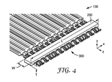
図4~図6において最も良くわかるように、ウェーハアセンブリ130は、間隔をあけて配置された実質的に平行な端子300の列を備える。図6を参照すると、各端子300は、嵌合部分320と、接触部分330と、嵌合部分320と接触部分330との間に配置された接続部分310と、を備えている。嵌合部分320は、図2及び図3に示されているPCB 110の対応する導電パッド112と無はんだ接触するために、接続部分310の第1の端部312から実装方向(z)に沿って延びる。嵌合部分320は、実装方向に弾性的に圧縮可能である。図6に示すように、一部の実施形態では、各端子300の嵌合部分320の少なくとも一部分がS字形である。接触部分330は、接続部分310の反対側にある第2の端部314から実装方向に沿って延びる。一部の実施形態によれば、各端子300の接触部分330は、対応するワイヤ400の端部420を受けるように構成された溝316を画定する。
As best seen in FIGS. 4-6, the
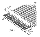
ウェーハアセンブリ130は、端子300の列の接続部分を覆うように成形され、この接続部分を封入する、ウェーハ200(図2及び図4~図7を参照されたい)を備える。図4に示すように、各ウェーハ200は、実装方向(z)に沿った幅(W)と、端子300の列の方向(x)に沿った長さ(L)と、を有する。各ウェーハ200は、列の方向及び実装方向に垂直な厚さ方向(y)に沿った厚さ(T)を有する。厚さは幅よりも実質的に小さく、幅は長さよりも実質的に小さい。
The
ここで図11及び図12を参照すると、一部の実施形態によれば、各ウェーハ200’は、ウェーハ200’の第1の主面220上にある少なくとも1つの第1の係止機構230と、ウェーハ200’の反対側にある第2の主面240上にある少なくとも1つの第2の係止機構235と、を備える。積層されたウェーハにおける隣り合うウェーハ200’の各対について、ウェーハを互いに固定するために、ウェーハの一方の少なくとも1つの第1の係止機構230は、ウェーハの他方の少なくとも1つの第2の係止機構235と係合する。例えば、各第1の係止機構230は突出部であってもよく、各第2の係止機構235は凹部であってもよい。
With reference to FIGS. 11 and 12, each wafer 200'with at least one
ウェーハアセンブリ130は、図1、図3、図5、図6、図7、及び図9に示されている複数のワイヤ400を備える。図6に示すように、各ワイヤ400は、対応する端子300の接触部分330において、終端領域410で終端処理される。一部の実施形態では、各ウェーハアセンブリ130について、ウェーハ200は、複数のワイヤ400の終端領域410を覆って封入するように成形することができる。
The
ウェーハアセンブリ130はまた、図5及び図7に示すように、ウェーハ200の主面220に隣接して配置され、かつ実質的にウェーハ200の幅及び長さ全体に沿って延びる遮蔽体500を備え得る。例えば、各ウェーハアセンブリ130の遮蔽体500は、矩形の板であってもよい。図2において最も良くわかるように、ウェーハアセンブリ130の積層体におけるウェーハ200は、隣り合うウェーハ200-1、200-2の各対について、ウェーハの一方200-1に対応する遮蔽体500が隣り合うウェーハ200-1、200-2の間に配置されるように積層される。図7に示す一部の実装形態では、各ウェーハアセンブリ130について、ウェーハ200は、ウェーハ200の主面220に凹部210を画定し、遮蔽体500は、凹部210内に配置される。
The
一部の実施形態によれば、図10に示すように、延長された遮蔽体500’が、ウェーハ200を越えて終端領域410に向かって延びて、これにより、平面視において、延長された遮蔽体500’が終端領域410の少なくとも一部分を覆う。
According to some embodiments, as shown in FIG. 10, the extended shield 500'extends beyond the
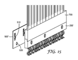
ここで図15を参照すると、一部の実施形態では、遮蔽体500’’は、隣り合うウェーハ200’の対の間に配置され、遮蔽体500’’において少なくとも1つの貫通開口520を画定する。隣り合うウェーハ200の対の少なくとも1つの第1の係止機構230及び第2の係止機構235(図11及び図12を参照されたい)は、遮蔽体500’’の少なくとも1つの貫通開口520を介して互いに係合する。
Now with reference to FIG. 15, in some embodiments, the
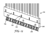
図13及び図14に示すように、各ウェーハアセンブリ130は、複数のワイヤ400の終端領域410を覆うように成形され、かつこの終端領域410を封入する内型700を備え、ウェーハアセンブリ130の積層体において内型700が内型700の積層体710を形成することができる。各ウェーハアセンブリ130の内型700は、対応する端子300の接触部分330の一部分332部を露出させる、少なくとも1つの開口720を画定することができる。ウェーハアセンブリ130の遮蔽体500’’は、内型700にわたって延び、かつ内型700を覆い、少なくとも1つの開口720を介して接触部分330の露出された部分332に物理的に接触する。一部の実装形態によれば、遮蔽体500’’は、内型700に向かって屈曲された少なくとも1つの可撓性タブ510を備える。可撓性タブ510は、内型700の開口720に挿入され、接触部分330の露出された部分332と物理的に接触する。図13及び図14に示すように、一部の実装形態では、各ウェーハアセンブリ130の内型700とウェーハ200’とは互いに隣接している。内型700は、ウェーハ200’の対応する第2の係合機構245と係合する第1の係合機構730を備える。例えば、第1の係合機構730は、ウェーハ200’の凹部内に嵌まる、内型700の突出部であり得る。
As shown in FIGS. 13 and 14, each
図1を再び参照すると、ハウジング600が、少なくとも積層されたウェーハ200及び複数のワイヤ400の終端領域410を封入する。例えば、ハウジング600は、少なくとも積層されたウェーハ200及び終端領域410を覆うように成形することができる。
Referring again to FIG. 1, the
PCB110にコネクタアセンブリ100を実装すると(図1、図2、及び図8を参照されたい)、各嵌合部分320が、実装方向に弾性的に圧縮される。一部の実施形態によれば、図8に示すように、ハウジング600は、嵌合部分320の実装方向への更なる圧縮を防止する止め具を備える。例えば、一部の実装形態では、止め具は、ハウジング600の底面620である。又はハウジング600の底面620に配置されている。一部の実装形態では、止め具は、ハウジング600の底面620から延びる突出部であってよい。図8及び図9を参照すると、嵌合部分320は、ハウジング600の底面620に画定された凹部610内で弾性的に圧縮することができる。
When the
図3に示すように、一部の実施形態によれば、ハウジング600は、図2に示すようなPCB 110の対応する導電パッド112と嵌合部分320を整列するように構成された整列機構630を備える。例えば、図3に示すように、整列機構630は、PCB110の対応する凹部114に挿入されるように構成された、少なくとも1対の間隔をあけて配置された突出部を有することができる。
As shown in FIG. 3, according to some embodiments, the
ハウジング600は、PCB110にコネクタアセンブリを取り付け、かつ固定するように構成された取り付け機構を備えることができる。例えば、取り付け機構は、ハウジング600の頂面660からハウジング600の対応する孔650内に挿入される少なくとも1対のねじ640を備えることができる。コネクタアセンブリ100がPCB110に実装され、かつ実装方向に沿ってPCB110に押し付けられ、端子300の嵌合部分320がPCB110の対応する導電パッド112に無はんだ接触し、実装方向に沿って弾性的に圧縮されるときに、1対のねじ640は、PCB110の頂面118からPCBの対応する孔116内に更に挿入され、PCB110にコネクタアセンブリ100を取り付ける。PCB110にコネクタアセンブリ100を取り付けることにより、圧縮された嵌合部分320の伸張を防止する。図3に示すように、取り付け機構はまた、1対のナット645を備えることができる。コネクタアセンブリがPCB 110に実装され、かつ実装方向に沿ってPCB 110に対して押し付けられると、ねじ640が回路基板110の底面119からのナット645と係合する。
The
図17Aは、ウェーハアセンブリ130の製造方法のフロー図である。図17Bは、回路基板110への実装及び実装方向(z)に沿った無はんだ電気接触のためのコネクタアセンブリ100の製造方法のフロー図である。
FIG. 17A is a flow chart of a manufacturing method of the
図17Aに示すように、ウェーハアセンブリを製造することは、間隔をあけて配置された実質的に平行な端子の列を準備すること1710を含む。各端子は、接続部と、嵌合部分と、接触部分と、を備える。嵌合部分は、PCBの対応する導電パッドと無はんだ接触するために、接続部分の第1の端部から実装方向に沿って延びる。嵌合部分は、実装方向に弾性的に圧縮可能である。接触部分は、接続部分の反対側にある第2の端部から実装方向に沿って延びる。ウェーハは、複数の端子の接続部分を覆うように成形される1720。ウェーハは、実装方向に沿った幅(W)と、端子の列の方向(x)に沿った長さ(L)と、を有する。複数のワイヤが、対応する端子の接触部分において、終端領域で終端処理される1730。遮蔽体は、ウェーハの主面に隣接して配置される1740。遮蔽体は、実質的にウェーハの幅及び長さ全体に沿って延びる。
As shown in FIG. 17A, manufacturing a wafer assembly involves preparing a row of substantially parallel terminals that are spaced apart. Each terminal includes a connection portion, a fitting portion, and a contact portion. The mating portion extends along the mounting direction from the first end of the connecting portion for non-solder contact with the corresponding conductive pad of the PCB. The mating portion can be elastically compressed in the mounting direction. The contact portion extends along the mounting direction from the second end on the opposite side of the connection portion. The wafer is formed in 1720 so as to cover the connection portion of a plurality of terminals. The wafer has a width (W) along the mounting direction and a length (L) along the direction (x) of the row of terminals. 1730 where a plurality of wires are terminated in the termination region at the contact portion of the corresponding terminal. The shield is placed adjacent to the main surface of the
(図17Bに示す)コネクタアセンブリの製造方法は、複数のウェーハアセンブリを製造することを含む1715。ウェーハアセンブリは、図17Aに関連して上述したように製造することができる。ウェーハアセンブリは、隣り合うウェーハの各対について、ウェーハの一方に対応する遮蔽体がウェーハの間に配置されるように積層されて、積層されたウェーハを形成する1725。少なくとも積層されたウェーハ及び複数のワイヤの終端領域が、ハウジングに封入される1735。例えば、積層されたウェーハ及び終端領域を封入することは、少なくとも積層されたウェーハ及び複数のワイヤの終端領域を覆うようにハウジングを成形することを含んでもよい。一部の実施形態では、内型は、複数のワイヤの終端領域を覆うように成形することができる。内型は、対応する端子の接触部分の一部分を露出する少なくとも1つの開口を画定する。ウェーハアセンブリの遮蔽体は、内型にわたって延び、かつ内型を覆い、少なくとも1つの開口を介して接触部分の露出された部分に物理的に接触する。
A method of manufacturing a connector assembly (shown in FIG. 17B) comprises manufacturing a plurality of wafer assemblies. 1715. Wafer assemblies can be manufactured as described above in connection with FIG. 17A. The wafer assembly is laminated for each pair of adjacent wafers so that a shield corresponding to one of the wafers is placed between the wafers to form a laminated wafer. At least the laminated wafers and the termination regions of the plurality of wires are encapsulated in the
本明細書に開示された実施形態は、下記を含む。 The embodiments disclosed herein include:
実施形態1.プリント回路基板(PCB)への実装及び実装方向に沿った無はんだ電気接触のためのコネクタアセンブリであって、
コネクタアセンブリは、ウェーハアセンブリの積層体と、ハウジングとを備え、
各ウェーハアセンブリは、
間隔をあけて配置された実質的に平行な端子の列であって、各端子が、
接続部分と、
PCBの対応する導電パッドと無はんだ接触するために、接続部分の第1の端部から実装方向に沿って延びており、実装方向に弾性的に圧縮可能である嵌合部分と、
接続部分の反対側にある第2の端部から実装方向に沿って延びる接触部分と、
を備える、端子の列と、
端子の列の接続部分を覆って封入するように成形されており、実装方向に沿った幅と、端子の列の方向に沿った長さとを有するウェーハと、
各ワイヤが、対応する端子の接触部分において終端領域で終端処理されている複数のワイヤと、
ウェーハの主面に隣接して配置されており、かつ実質的にウェーハの幅及び長さ全体に沿って延びる遮蔽体であって、ウェーハアセンブリの積層体におけるウェーハは、隣り合うウェーハの各対に対して、ウェーハの一方に対応する遮蔽体がウェーハの間に配置されるように積層された遮蔽体と、
を有し、
前記ハウジングは、少なくとも積層されたウェーハ及び複数のワイヤの終端領域を封入する、コネクタアセンブリ。
Embodiment 1. A connector assembly for mounting on a printed circuit board (PCB) and solder-free electrical contact along the mounting direction.
The connector assembly comprises a laminate of wafer assemblies and a housing.
Each wafer assembly
A row of substantially parallel terminals arranged at intervals, with each terminal
The connection part and
A fitting portion that extends along the mounting direction from the first end of the connection and is elastically compressible in the mounting direction for non-solder contact with the corresponding conductive pad of the PCB.
A contact portion extending along the mounting direction from the second end on the opposite side of the connection portion,
With a row of terminals and
A wafer that is molded to cover and enclose the connection portion of a row of terminals and has a width along the mounting direction and a length along the direction of the row of terminals.
Multiple wires, each of which is terminated in the termination region at the contact of the corresponding terminal,
A shield that is located adjacent to the main surface of the wafer and extends substantially along the width and length of the wafer, the wafers in the wafer assembly laminate are on each pair of adjacent wafers. On the other hand, a shield laminated so that a shield corresponding to one of the wafers is arranged between the wafers,
Have,
The housing is a connector assembly that encloses at least laminated wafers and termination areas for multiple wires.
実施形態2.各嵌合部分が実装方向に弾性的に圧縮されており、ハウジングの止め具が嵌合部分の実装方向への更なる圧縮を防止する、PCBに実装された実施形態1に記載のコネクタアセンブリ。 Embodiment 2. 12. The connector assembly according to embodiment 1, mounted on a PCB, wherein each mating portion is elastically compressed in the mounting direction and a fastener in the housing prevents further compression of the mating portion in the mounting direction.
実施形態3.止め具がハウジングの底面である、実施形態2に記載のコネクタアセンブリ。 Embodiment 3. The connector assembly according to embodiment 2, wherein the fastener is the bottom surface of the housing.
実施形態4.嵌合部分が、ハウジングの底面に画定された凹部内で弾性的に圧縮される、実施形態2の記載のコネクタアセンブリ。 Embodiment 4. 2. The connector assembly according to embodiment 2, wherein the mating portion is elastically compressed within a recess defined in the bottom surface of the housing.
実施形態5.各ウェーハが、列の方向及び実装方向に垂直な厚さ方向に沿った厚さを有し、厚さが幅よりも実質的に小さく、幅が長さよりも実質的に小さい、実施形態1から4のいずれか一実施形態に記載のコネクタアセンブリ。 Embodiment 5. From Embodiment 1, where each wafer has a thickness along the thickness direction perpendicular to the row direction and the mounting direction, the thickness being substantially less than the width and the width being substantially less than the length. 4. The connector assembly according to any one embodiment.
実施形態6.各端子の嵌合部分の少なくとも一部分がS字形である、実施形態1から5のいずれか一実施形態に記載のコネクタアセンブリ。 Embodiment 6. The connector assembly according to any one of embodiments 1 to 5, wherein at least a portion of the fitting portion of each terminal is S-shaped.
実施形態7.各端子の接触部分が、対応するワイヤの端部を受けるための溝を画定する、実施形態1から6のいずれか一実施形態に記載のコネクタアセンブリ。 Embodiment 7. The connector assembly according to any one of embodiments 1 to 6, wherein the contact portion of each terminal defines a groove for receiving the end of the corresponding wire.
実施形態8.各ウェーハアセンブリの遮蔽体が矩形の板である、実施形態1から7のいずれか一実施形態に記載のコネクタアセンブリ。 Embodiment 8. The connector assembly according to any one of embodiments 1 to 7, wherein the shield of each wafer assembly is a rectangular plate.
実施形態9.少なくとも1つのウェーハアセンブリについて、遮蔽体が、ウェーハを越えて終端領域に向かって延びており、これにより、平面視において、遮蔽体が終端領域の少なくとも一部分を覆う、実施形態1から8のいずれか一実施形態に記載のコネクタアセンブリ。 Embodiment 9. For at least one wafer assembly, one of embodiments 1-8, wherein the shield extends beyond the wafer towards the termination region, whereby the shield covers at least a portion of the termination region in plan view. The connector assembly according to one embodiment.
実施形態10.ハウジングは、PCBの対応する導電パッドと嵌合部分を整列するための整列手段を備える、実施形態1から9のいずれか一実施形態に記載のコネクタアセンブリ。 Embodiment 10. The connector assembly according to any one of embodiments 1 to 9, wherein the housing comprises an alignment means for aligning the mating portion with the corresponding conductive pad of the PCB.
実施形態11.整列手段は、PCBの対応する凹部に挿入されるように構成された、少なくとも1対の間隔をあけて配置された突出部を備える、実施形態10の一実施形態に記載のコネクタアセンブリ。 Embodiment 11. The connector assembly according to one embodiment of Embodiment 10, wherein the alignment means comprises at least a pair of spaced protrusions configured to be inserted into the corresponding recesses of the PCB.
実施形態12.ハウジングは、PCBにコネクタアセンブリを取り付け、かつ固定するための取り付け手段を備える、実施形態1から11のいずれか一実施形態に記載のコネクタアセンブリ。 Embodiment 12. The connector assembly according to any one of embodiments 1 to 11, wherein the housing comprises mounting means for mounting and fixing the connector assembly to the PCB.
実施形態13.取り付け手段は、ハウジングの頂面からハウジングの対応する孔内に挿入される少なくとも1対のねじを備え、コネクタアセンブリがPCBに実装されており、かつ実装方向に沿ってPCBに押し付けられ、端子の嵌合部分はPCBの対応する導電パッドに無はんだ接触し、実装方向に沿って弾性的に圧縮されるときに、1対のねじが、PCBの頂面からPCBの対応する孔内に更に挿入され、PCBにコネクタアセンブリを取り付け、PCBにコネクタアセンブリを取り付けることにより、圧縮された嵌合部分の伸張を防止する、実施形態12に記載のコネクタアセンブリ。 Embodiment 13. The mounting means comprises at least a pair of screws inserted from the top surface of the housing into the corresponding holes in the housing, the connector assembly mounted on the PCB and pressed against the PCB along the mounting direction and of the terminals. When the mating part makes non-solder contact with the corresponding conductive pad of the PCB and is elastically compressed along the mounting direction, a pair of screws is further inserted into the corresponding hole of the PCB from the top surface of the PCB. 12. The connector assembly according to embodiment 12, wherein the connector assembly is attached to the PCB and the connector assembly is attached to the PCB to prevent expansion of the compressed fitting portion.
実施形態14.取り付け手段は、1対のナットを更に備え、コネクタアセンブリがPCBに実装されており、かつ実装方向に沿ってPCBに対して押し付けられると、ねじが回路基板の底面からのナットと係合する、実施形態13に記載のコネクタアセンブリ。 Embodiment 14. The mounting means further comprises a pair of nuts, the connector assembly is mounted on the PCB, and when pressed against the PCB along the mounting direction, the screw engages the nut from the bottom of the circuit board. The connector assembly according to the thirteenth embodiment.
実施形態15.各ウェーハアセンブリについて、ウェーハが、ウェーハの主面に凹部を画定し、遮蔽体が、凹部内に配置されている、実施形態1から14のいずれか一実施形態に記載のコネクタアセンブリ。 Embodiment 15. The connector assembly according to any one of embodiments 1 to 14, wherein for each wafer assembly, the wafer defines a recess in the main surface of the wafer and the shield is located in the recess.
実施形態16.ハウジングは、少なくとも積層されたウェーハ及び複数のワイヤの終端領域を覆って封入するように成形されている、実施形態1から15のいずれか一実施形態に記載のコネクタアセンブリ。 Embodiment 16. The connector assembly according to any one of embodiments 1 to 15, wherein the housing is molded to cover and enclose at least a laminated wafer and termination regions of a plurality of wires.
実施形態17.各ウェーハは、ウェーハの第1の主面上にある少なくとも1つの第1の係止機構と、ウェーハの反対側にある第2の主面上にある少なくとも1つの第2の係止機構と、を備えて、積層されたウェーハにおける隣り合うウェーハの各対について、ウェーハを互いに固定するために、ウェーハの一方の少なくとも1つの第1の係止機構が、ウェーハの他方の少なくとも1つの第2の係止機構と係合する、実施形態1から16のいずれか一実施形態に記載のコネクタアセンブリ。 Embodiment 17. Each wafer has at least one first locking mechanism on the first main surface of the wafer and at least one second locking mechanism on the second main surface opposite the wafer. At least one first locking mechanism on one side of the wafer is provided with at least one second locking mechanism on the other side of the wafer to secure the wafers to each other for each pair of adjacent wafers in a laminated wafer. The connector assembly according to any one of embodiments 1 to 16, which engages with a locking mechanism.
実施形態18.各第1の係止機構が突出部であり、各第2の係止機構が凹部である、実施形態17に記載のコネクタアセンブリ。 Embodiment 18. 17. The connector assembly according to embodiment 17, wherein each first locking mechanism is a protrusion and each second locking mechanism is a recess.
実施形態19.隣り合うウェーハの対の間に配置された遮蔽体は、内部に少なくとも1つの貫通開口を画定し、隣り合うウェーハの対の少なくとも1つの第1の係止機構及び第2の係止機構は、遮蔽体の少なくとも1つの貫通開口を介して互いに係合する、実施形態18に記載のコネクタアセンブリ。 Embodiment 19. The shield placed between the pairs of adjacent wafers defines at least one through opening inside, and the at least one first locking mechanism and the second locking mechanism of the pair of adjacent wafers are. 18. The connector assembly according to embodiment 18, which engages with each other through at least one through opening of the shield.
実施形態20.各ウェーハアセンブリは、複数のワイヤの終端領域を覆って封入するように成形された内型を更に備えて、ウェーハアセンブリの積層体において内型が内型の積層体を形成する、実施形態1から19のいずれか一実施形態に記載のコネクタアセンブリ。 20. From Embodiment 1, each wafer assembly further comprises an inner die formed to cover and enclose a plurality of wire termination regions, and the inner die forms an inner die laminate in the wafer assembly laminate. 19. The connector assembly according to any one embodiment.
実施形態21.各ウェーハアセンブリの内型は、対応する端子の接触部分の一部分を露出する少なくとも1つの開口を画定し、ウェーハアセンブリの遮蔽体が、内型にわたって延び、かつ内型を覆い、少なくとも1つの開口を介して接触部分の露出された部分に物理的に接触する、実施形態20に記載のコネクタアセンブリ。 21. Embodiment 21. The inner mold of each wafer assembly defines at least one opening that exposes a portion of the contact area of the corresponding terminal, and the wafer assembly shield extends over the inner mold and covers the inner mold, making at least one opening. 20. The connector assembly according to embodiment 20, wherein the exposed portion of the contact portion is physically contacted through.
実施形態22.遮蔽体ha、内型に向かって屈曲された少なくとも1つの可撓性タブを備え、少なくとも1つの可撓性タブが、内型の少なくとも1つの開口に挿入され、接触部分の露出された部分と物理的に接触する、実施形態21に記載のコネクタアセンブリ。 Embodiment 22. The shield ha comprises at least one flexible tab bent towards the inner mold, the at least one flexible tab being inserted into at least one opening of the inner mold with an exposed portion of the contact portion. 21. The connector assembly according to embodiment 21, which is in physical contact.
実施形態23.各ウェーハアセンブリの内型とウェーハとが互いに隣接し、内型は、ウェーハの対応する第2の係合機構と係合する第1の係合機構を有する、実施形態20に記載のコネクタアセンブリ。 23. 20. The connector assembly according to embodiment 20, wherein the inner die of each wafer assembly and the wafer are adjacent to each other and the inner die has a first engaging mechanism that engages with a corresponding second engaging mechanism of the wafer.
実施形態24.各ウェーハアセンブリについて、ウェーハが更に、複数のワイヤの終端領域を覆って封入するように成形されている、実施形態1から23のいずれか一実施形態に記載のコネクタアセンブリ。 Embodiment 24. The connector assembly according to any one of embodiments 1 to 23, wherein for each wafer assembly, the wafer is further formed to cover and encapsulate a terminal region of a plurality of wires.
実施形態25.プリント回路基板(PCB)への実装及び実装方向に沿った無はんだ電気接触のためのコネクタアセンブリの製造方法であって、本方法は、
(a)ウェーハアセンブリを製造するステップであって、
(i)間隔をあけて配置された実質的に平行な端子の列を準備する工程であって、各端子が、
接続部分と、
PCBの対応する導電パッドと無はんだ接触するために、接続部分の第1の端部から実装方向に沿って延びる嵌合部分であって、嵌合部分が実装方向に弾性的に圧縮可能である、嵌合部分と、
接続部分の反対側にある第2の端部から実装方向に沿って延びる接触部分と、
を備える、端子の列と、
(ii)複数の端子の接続部分を覆うようにウェーハを成形するステップであって、ウェーハが、実装方向に沿った幅と、端子の列の方向に沿った長さと、を有する、ステップと、
(iii)複数のワイヤを準備し、かつ対応する端子の接触部分において、終端領域で各ワイヤを終端処理するステップと、
(iv)ウェーハの主面に隣接して遮蔽体を配置するステップであって、遮蔽体が実質的にウェーハの幅及び長さ全体に沿って延びる、ステップと、
を含む、ステップと、
(b)複数のウェーハアセンブリを形成するために、ステップ(a)を少なくとも1回繰り返すステップと、
(c)積層されたウェーハを形成するために、複数のウェーハアセンブリにおけるウェーハを、隣り合うウェーハの各対について、ウェーハの一方に対応する遮蔽体がウェーハの間に配置されるように積層するステップと、
(d)少なくとも積層されたウェーハ及び複数のワイヤの終端領域をハウジングに封入するステップと、
を含む、方法。
Embodiment 25. A method for manufacturing a connector assembly for mounting on a printed circuit board (PCB) and solder-free electrical contact along the mounting direction.
(A) A step of manufacturing a wafer assembly.
(I) A step of preparing a row of substantially parallel terminals arranged at intervals, wherein each terminal is
The connection part and
A fitting portion extending along the mounting direction from the first end of the connecting portion for non-solder contact with the corresponding conductive pad of the PCB, the fitting portion being elastically compressible in the mounting direction. , Fitting part and
A contact portion extending along the mounting direction from the second end on the opposite side of the connection portion,
With a row of terminals and
(Ii) A step of forming a wafer so as to cover a connection portion of a plurality of terminals, wherein the wafer has a width along the mounting direction and a length along the direction of a row of terminals.
(Iii) A step of preparing a plurality of wires and terminating each wire in the termination region at the contact portion of the corresponding terminal.
(Iv) A step of placing the shield adjacent to the main surface of the wafer, wherein the shield extends substantially along the width and length of the wafer.
Including steps and
(B) A step of repeating step (a) at least once to form a plurality of wafer assemblies.
(C) In order to form a laminated wafer, a step of laminating wafers in a plurality of wafer assemblies so that a shield corresponding to one of the wafers is arranged between the wafers for each pair of adjacent wafers. When,
(D) A step of encapsulating at least laminated wafers and termination regions of a plurality of wires in a housing.
Including, how.
実施形態26.ステップ(iii)において、端子の接触部分における複数のワイヤの終端処理を実質的に同時に行う、実施形態25に記載の方法。 Embodiment 26. 25. The method of embodiment 25, wherein in step (iii), termination processing of a plurality of wires at the contact portion of the terminal is performed substantially simultaneously.
実施形態27.ステップ(d)において、ハウジングが、少なくとも積層されたウェーハ及び複数のワイヤの終端領域を覆うように成形される、実施形態25又は26に記載の方法。 Embodiment 27. 25. The method of embodiment 25 or 26, wherein in step (d) the housing is formed to cover at least the laminated wafers and the termination regions of the plurality of wires.
実施形態28.複数のワイヤの終端領域を覆うように内型を成形するステップであって、内型が、対応する端子の接触部分の一部分を露出する少なくとも1つの開口を画定し、ウェーハアセンブリの遮蔽体が、内型にわたって延び、かつ内型を覆い、少なくとも1つの開口を介して接触部分の露出された部分に物理的に接触する、ステップを更に含む、実施形態25から27のいずれか一実施形態に記載の方法。 Embodiment 28. In the step of forming the inner mold so as to cover the terminal area of a plurality of wires, the inner mold defines at least one opening that exposes a part of the contact portion of the corresponding terminal, and the shield of the wafer assembly. 25. The embodiment of any one of embodiments 25-27, further comprising a step of extending over and covering the inner mold and physically contacting the exposed portion of the contact portion through at least one opening. the method of.
別途断りがない限り、本明細書及び特許請求の範囲で用いる加工寸法(feature size)、量、及び物理的特性を表す全ての数は、全ての場合において、用語「約」によって修飾されていると理解するものとする。したがって、特に反対の指示のない限り、上記明細書及び添付の特許請求の範囲に記載されている数値パラメータは、本明細書で開示される教示を利用して当業者が得ようとする所望の特性に応じて変動し得る近似値である。端点による数値範囲の使用は、その範囲内の全ての数(例えば、1~5は、1、1.5、2、2.75、3、3.80、4、及び5を含む)、及びその範囲内の任意の範囲を含む。 Unless otherwise noted, all numbers representing the feature size, quantity, and physical properties used herein and in the claims are in all cases modified by the term "about". It shall be understood. Accordingly, unless otherwise indicated, the numerical parameters described in the specification and the appended claims are desired to be obtained by those skilled in the art using the teachings disclosed herein. It is an approximate value that can vary depending on the characteristics. The use of numerical ranges by endpoints is for all numbers within that range (eg, 1-5 include 1, 1.5, 2, 2.75, 3, 3.80, 4, and 5), and Includes any range within that range.
これら実施形態の様々な修正及び変更が、当業者には明らかとなるものであり、本開示の本範囲は、本明細書に記載されている例示的実施形態に限定されるものではないことを理解されたい。例えば、1つの開示実施形態の特徴は、別途指示のない限り、他の開示実施形態全てにも適用され得ることを、読者は前提とすべきである。 Various modifications and changes to these embodiments will be apparent to those of skill in the art, and the scope of this disclosure is not limited to the exemplary embodiments described herein. I want to be understood. For example, the reader should assume that the characteristics of one disclosure embodiment can be applied to all other disclosure embodiments, unless otherwise indicated.
Claims (4)
前記コネクタアセンブリは、ウェーハアセンブリの積層体と、ハウジングとを備え、
各ウェーハアセンブリは、
間隔をあけて配置された実質的に平行な端子の列であって、各端子が、
接続部分と、
PCBの対応する導電パッドと無はんだ接触するために、前記接続部分の第1の端部から前記実装方向に沿って延びており、前記実装方向に弾性的に圧縮可能であるS字形部分と、
前記接続部分の反対側にある第2の端部から前記実装方向に沿って延びる接触部分と、
を備える、端子の列と、
前記端子の列の前記接続部分を覆って封入するように成形されており、かつ、前記実装方向に沿った幅と、前記端子の前記列の方向に沿った長さとを有するウェーハと、
各ワイヤが、対応する端子の前記接触部分において終端領域で終端処理されている複数のワイヤと、
前記ウェーハの主面に隣り合って配置されており、かつ実質的に前記ウェーハの前記幅及び前記長さ全体に沿って延びる遮蔽体であって、前記ウェーハアセンブリの積層体において前記ウェーハは、隣り合うウェーハの各対に対して、前記ウェーハの一方に対応する前記遮蔽体が前記ウェーハの間に配置されるように積層された遮蔽体と、を有し、
前記ハウジングは、少なくとも前記積層されたウェーハ及び前記複数のワイヤの前記終端領域を封入する、コネクタアセンブリ。 A connector assembly for mounting on a printed circuit board (PCB) and solder-free electrical contact along the mounting direction.
The connector assembly comprises a laminate of wafer assemblies and a housing.
Each wafer assembly
A row of substantially parallel terminals arranged at intervals, with each terminal
The connection part and
An S-shaped portion that extends from the first end of the connection portion along the mounting direction and is elastically compressible in the mounting direction for non-solder contact with the corresponding conductive pad of the PCB.
A contact portion extending from the second end on the opposite side of the connection portion along the mounting direction, and a contact portion.
With a row of terminals and
A wafer that is molded to cover and encapsulate the connection portion of the row of terminals and has a width along the mounting direction and a length along the direction of the row of terminals.
Each wire has a plurality of wires terminated in the termination region at said contact portion of the corresponding terminal.
A shield that is disposed adjacent to the main surface of the wafer and extends substantially along the width and length of the wafer, wherein the wafers are adjacent to each other in the laminate of the wafer assembly. For each pair of matching wafers, there is a shield laminated so that the shield corresponding to one of the wafers is arranged between the wafers.
The housing is a connector assembly that encapsulates at least the laminated wafer and the termination region of the plurality of wires.
前記ウェーハアセンブリの前記遮蔽体は、前記内型にわたって延び、かつ前記内型を覆い、前記少なくとも1つの開口を通して前記接触部分の露出された部分に物理的に接触する、請求項2に記載のコネクタアセンブリ。 The inner mold of each wafer assembly defines at least one opening that exposes a portion of the contact portion of the corresponding terminal.
The connector according to claim 2, wherein the shield of the wafer assembly extends over the inner mold and covers the inner mold and physically contacts the exposed portion of the contact portion through the at least one opening. assembly.
(a)ウェーハアセンブリを製造するステップであって、
(i)間隔をあけて配置された実質的に平行な端子の列を準備する工程であって、各端子が、
接続部分と、
PCBの対応する導電パッドと無はんだ接触するために、前記接続部分の第1の端部から前記実装方向に沿って延びており、前記実装方向に弾性的に圧縮可能であるS字形部分と、
前記接続部分の反対側にある第2の端部から前記実装方向に沿って延びる接触部分と、
を備える、工程と、
(ii)前記複数の端子の前記接続部分を覆うようにウェーハを成形する工程であって、前記ウェーハが、前記実装方向に沿った幅と、前記端子の前記列の方向に沿った長さとを有する、工程と、
(iii)複数のワイヤを準備し、かつ対応する端子の前記接触部分において、終端領域で各ワイヤを終端処理する工程と、
(iv)前記ウェーハの主面に隣り合う遮蔽体を配置する工程であって、前記遮蔽体が実質的に前記ウェーハの前記幅及び前記長さ全体に沿って延びる、工程と、
を含む、ステップと、
(b)複数のウェーハアセンブリを形成するために、ステップ(a)を少なくとも1回繰り返すステップと、
(c)積層されたウェーハを形成するために、前記複数のウェーハアセンブリにおいて前記ウェーハを積層し、これにより隣り合うウェーハの各対に対して、前記ウェーハの一方に対応する前記遮蔽体が前記ウェーハの間に配置される、ステップと、
(d)少なくとも前記積層されたウェーハ及び前記複数のワイヤの前記終端領域をハウジングに封入するステップと、
を含む、方法。 A method for manufacturing a connector assembly for mounting on a printed circuit board (PCB) and solder-free electrical contact along the mounting direction.
(A) A step of manufacturing a wafer assembly.
(I) A step of preparing a row of substantially parallel terminals arranged at intervals, wherein each terminal is
The connection part and
An S-shaped portion that extends from the first end of the connection portion along the mounting direction and is elastically compressible in the mounting direction for non-solder contact with the corresponding conductive pad of the PCB.
A contact portion extending from the second end on the opposite side of the connection portion along the mounting direction, and a contact portion.
With the process and
(Ii) A step of forming a wafer so as to cover the connection portion of the plurality of terminals, wherein the wafer has a width along the mounting direction and a length along the direction of the row of the terminals. Have, process and
(Iii) A step of preparing a plurality of wires and terminating each wire in the termination region at the contact portion of the corresponding terminal.
(Iv) A step of arranging adjacent shields on the main surface of the wafer, wherein the shield extends substantially along the width and length of the wafer.
Including steps and
(B) A step of repeating step (a) at least once to form a plurality of wafer assemblies.
(C) In order to form a laminated wafer, the wafers are laminated in the plurality of wafer assemblies, whereby for each pair of adjacent wafers, the shield corresponding to one of the wafers is the wafer. Placed between the steps and
(D) A step of enclosing at least the laminated wafer and the end region of the plurality of wires in the housing.
Including the method.
Priority Applications (1)
| Application Number | Priority Date | Filing Date | Title |
|---|---|---|---|
| JP2022014589A JP2022048298A (en) | 2016-09-29 | 2022-02-02 | Connector assembly for solderless mounting to circuit board |
Applications Claiming Priority (3)
| Application Number | Priority Date | Filing Date | Title |
|---|---|---|---|
| US201662401322P | 2016-09-29 | 2016-09-29 | |
| US62/401,322 | 2016-09-29 | ||
| PCT/IB2017/055968 WO2018060922A1 (en) | 2016-09-29 | 2017-09-28 | Connector assembly for solderless mounting to a circuit board |
Related Child Applications (1)
| Application Number | Title | Priority Date | Filing Date |
|---|---|---|---|
| JP2022014589A Division JP2022048298A (en) | 2016-09-29 | 2022-02-02 | Connector assembly for solderless mounting to circuit board |
Publications (3)
| Publication Number | Publication Date |
|---|---|
| JP2019530182A JP2019530182A (en) | 2019-10-17 |
| JP2019530182A5 JP2019530182A5 (en) | 2020-11-12 |
| JP7019681B2 true JP7019681B2 (en) | 2022-02-15 |
Family
ID=60083373
Family Applications (2)
| Application Number | Title | Priority Date | Filing Date |
|---|---|---|---|
| JP2019517051A Active JP7019681B2 (en) | 2016-09-29 | 2017-09-28 | Connector assembly for solder-free mounting on circuit boards |
| JP2022014589A Withdrawn JP2022048298A (en) | 2016-09-29 | 2022-02-02 | Connector assembly for solderless mounting to circuit board |
Family Applications After (1)
| Application Number | Title | Priority Date | Filing Date |
|---|---|---|---|
| JP2022014589A Withdrawn JP2022048298A (en) | 2016-09-29 | 2022-02-02 | Connector assembly for solderless mounting to circuit board |
Country Status (4)
| Country | Link |
|---|---|
| US (1) | US11462845B2 (en) |
| JP (2) | JP7019681B2 (en) |
| CN (1) | CN109792114B (en) |
| WO (1) | WO2018060922A1 (en) |
Families Citing this family (6)
| Publication number | Priority date | Publication date | Assignee | Title |
|---|---|---|---|---|
| US11462845B2 (en) * | 2016-09-29 | 2022-10-04 | 3M Innovative Properties Company | Connector assembly for solderless mounting to a circuit board |
| US10700452B2 (en) | 2018-05-14 | 2020-06-30 | 3M Innovative Properties Company | Connector terminal |
| TW202147717A (en) * | 2020-01-27 | 2021-12-16 | 美商安芬諾股份有限公司 | Electrical connector with high speed mounting interface |
| CN111244686A (en) * | 2020-03-18 | 2020-06-05 | 东莞立讯技术有限公司 | Adapter connector |
| WO2022185138A1 (en) * | 2021-03-05 | 2022-09-09 | 3M Innovative Properties Company | Cable assembly including printed circuit board |
| CN113224597B (en) * | 2021-04-16 | 2023-04-14 | 领翌技术(横琴)有限公司 | Cable connector and electronic device |
Citations (6)
| Publication number | Priority date | Publication date | Assignee | Title |
|---|---|---|---|---|
| US6776629B2 (en) | 2002-06-13 | 2004-08-17 | Fci Americas Technology, Inc. | Connector for mounting to mating connector, and shield therefor |
| JP2008018633A (en) | 2006-07-13 | 2008-01-31 | Sumitomo Wiring Syst Ltd | Manufacturing method for insert-molded article, and molding die for insert-molding |
| JP2014157718A (en) | 2013-02-15 | 2014-08-28 | Hitachi Metals Ltd | Cable connector and cable assembly |
| US8926342B2 (en) | 2011-10-24 | 2015-01-06 | Ardent Concepts, Inc. | Controlled-impedance cable termination using compliant interconnect elements |
| WO2015079845A1 (en) | 2013-11-29 | 2015-06-04 | 株式会社村田製作所 | Method for generating intermetallic compound, and method for connecting articles to be connected by using intermetallic compound |
| WO2016112384A1 (en) | 2015-01-11 | 2016-07-14 | Molex, Llc | Wire to board connectors suitable for use in bypass routing assemblies |
Family Cites Families (56)
| Publication number | Priority date | Publication date | Assignee | Title |
|---|---|---|---|---|
| US3586962A (en) * | 1969-02-28 | 1971-06-22 | Edward C Rebstock | Battery cell monitoring apparatus |
| US4095867A (en) * | 1974-10-10 | 1978-06-20 | Bunker Ramo Corporation | Component connection system |
| US4006388A (en) * | 1975-03-03 | 1977-02-01 | Hughes Aircraft Company | Thermally controlled electronic system package |
| US4533187A (en) * | 1983-01-06 | 1985-08-06 | Augat Inc. | Dual beam connector |
| US4615578A (en) * | 1984-12-05 | 1986-10-07 | Raychem Corporation | Mass termination device and connection assembly |
| US4619490A (en) * | 1984-12-18 | 1986-10-28 | Raychem Corporation | Guidance and retention device and connector assembly |
| US4591225A (en) * | 1985-01-14 | 1986-05-27 | Molex Incorporated | Arrangement for interconnecting a printed circuit board with a multi-conductor cable |
| SE450534B (en) * | 1985-10-03 | 1987-06-29 | Bofors Ab | MULTIPLE CONTACT |
| US4770639A (en) * | 1987-03-02 | 1988-09-13 | Switchcraft, Inc. | Channelized jackfield |
| JPH0414372U (en) * | 1990-05-28 | 1992-02-05 | ||
| US6409521B1 (en) * | 1997-05-06 | 2002-06-25 | Gryphics, Inc. | Multi-mode compliant connector and replaceable chip module utilizing the same |
| US6089920A (en) * | 1998-05-04 | 2000-07-18 | Micron Technology, Inc. | Modular die sockets with flexible interconnects for packaging bare semiconductor die |
| US6923681B1 (en) | 1998-05-22 | 2005-08-02 | Raytheon Company | Electrical assembly for solderless interconnection of circuit boards in a stacked configuration |
| US6441315B1 (en) * | 1998-11-10 | 2002-08-27 | Formfactor, Inc. | Contact structures with blades having a wiping motion |
| US7126220B2 (en) * | 2002-03-18 | 2006-10-24 | Nanonexus, Inc. | Miniaturized contact spring |
| US6888362B2 (en) * | 2000-11-09 | 2005-05-03 | Formfactor, Inc. | Test head assembly for electronic components with plurality of contoured microelectronic spring contacts |
| US6183269B1 (en) * | 2000-01-27 | 2001-02-06 | Itt Manufacturing Enterprises, Inc. | Termination adaptor for PCB |
| US6641430B2 (en) * | 2000-02-14 | 2003-11-04 | Advantest Corp. | Contact structure and production method thereof and probe contact assembly using same |
| US6478624B2 (en) | 2000-06-29 | 2002-11-12 | Robinson Nugent, Inc. | High speed connector |
| US7011530B2 (en) * | 2002-05-24 | 2006-03-14 | Sitaraman Suresh K | Multi-axis compliance spring |
| US7270573B2 (en) * | 2002-08-30 | 2007-09-18 | Fci Americas Technology, Inc. | Electrical connector with load bearing features |
| US6926553B2 (en) * | 2003-06-19 | 2005-08-09 | Hon Hai Precision Ind. Co., Ltd. | Cable assembly with improved grounding means |
| DE10300532B4 (en) * | 2003-01-09 | 2010-11-11 | Qimonda Ag | System having at least one test socket device for testing semiconductor devices |
| US7244125B2 (en) * | 2003-12-08 | 2007-07-17 | Neoconix, Inc. | Connector for making electrical contact at semiconductor scales |
| WO2004093252A2 (en) * | 2003-04-11 | 2004-10-28 | Neoconix, Inc. | Electrical connector and method for making |
| US6870381B2 (en) * | 2003-06-27 | 2005-03-22 | Formfactor, Inc. | Insulative covering of probe tips |
| US6971929B2 (en) * | 2004-03-31 | 2005-12-06 | Itt Manufacturing Enterprises, Inc. | Modular high density connector |
| US7371117B2 (en) * | 2004-09-30 | 2008-05-13 | Amphenol Corporation | High speed, high density electrical connector |
| US20060079102A1 (en) * | 2004-10-13 | 2006-04-13 | The Ludlow Company Lp | Cable terminal with flexible contacts |
| KR100687027B1 (en) * | 2005-02-22 | 2007-02-26 | 세크론 주식회사 | Structure and method for manufacturing probe and prob card |
| CN201075451Y (en) * | 2007-06-21 | 2008-06-18 | 富士康(昆山)电脑接插件有限公司 | Electric Connector |
| US8469720B2 (en) * | 2008-01-17 | 2013-06-25 | Amphenol Corporation | Electrical connector assembly |
| KR20090082783A (en) * | 2008-01-28 | 2009-07-31 | 삼성전자주식회사 | Prove card assembly for electrical die sorting process |
| US8342888B2 (en) * | 2008-08-28 | 2013-01-01 | Molex Incorporated | Connector with overlapping ground configuration |
| WO2010039188A1 (en) * | 2008-09-23 | 2010-04-08 | Amphenol Corporation | High density electrical connector |
| KR20100110023A (en) * | 2009-04-02 | 2010-10-12 | 삼성전기주식회사 | Connetor |
| JP2011070776A (en) * | 2009-09-23 | 2011-04-07 | Sumitomo Wiring Syst Ltd | Male connector, and printed board equipped therewith |
| TWM377746U (en) * | 2009-09-30 | 2010-04-01 | Hon Hai Prec Ind Co Ltd | Electrical connector |
| EP2532057A4 (en) * | 2010-02-01 | 2013-08-21 | 3M Innovative Properties Co | Electrical connector and assembly |
| WO2011140438A2 (en) * | 2010-05-07 | 2011-11-10 | Amphenol Corporation | High performance cable connector |
| US8485831B2 (en) * | 2011-01-06 | 2013-07-16 | International Business Machines Corporation | Tall mezzanine connector |
| US8636543B2 (en) * | 2011-02-02 | 2014-01-28 | Amphenol Corporation | Mezzanine connector |
| DE102011006867A1 (en) * | 2011-04-06 | 2012-10-11 | Robert Bosch Gmbh | Connector for direct contacting on a printed circuit board |
| US9142921B2 (en) * | 2013-02-27 | 2015-09-22 | Molex Incorporated | High speed bypass cable for use with backplanes |
| EP2965386A4 (en) * | 2013-03-04 | 2017-01-18 | 3M Innovative Properties Company | Electrical interconnection system and electrical connectors for the same |
| DE102013008324A1 (en) * | 2013-05-08 | 2014-11-13 | Feinmetall Gmbh | Electrical contacting device |
| CN105580210B (en) * | 2013-09-04 | 2017-07-07 | 莫列斯有限公司 | It is provided with the connector system of bypass cable |
| CN110247219B (en) * | 2014-01-22 | 2021-06-15 | 安费诺有限公司 | Electrical connector |
| TWI637568B (en) * | 2015-01-11 | 2018-10-01 | 莫仕有限公司 | Circuit board bypass assembly and its components |
| CN204464524U (en) * | 2015-01-23 | 2015-07-08 | 康舒电子(东莞)有限公司 | Exempt from the power terminal assemblies welded |
| DE112016002059T5 (en) * | 2015-05-04 | 2018-01-18 | Molex, Llc | Computing device that uses a bypass unit |
| US11462845B2 (en) * | 2016-09-29 | 2022-10-04 | 3M Innovative Properties Company | Connector assembly for solderless mounting to a circuit board |
| WO2018231822A1 (en) * | 2017-06-13 | 2018-12-20 | Molex, Llc | High density receptacle |
| US10522931B2 (en) * | 2017-07-28 | 2019-12-31 | Molex, Llc | High density receptacle |
| US10944214B2 (en) * | 2017-08-03 | 2021-03-09 | Amphenol Corporation | Cable connector for high speed interconnects |
| JP2022544561A (en) * | 2019-10-24 | 2022-10-19 | モレックス エルエルシー | connector assembly |
-
2017
- 2017-09-28 US US16/326,457 patent/US11462845B2/en active Active
- 2017-09-28 WO PCT/IB2017/055968 patent/WO2018060922A1/en active Application Filing
- 2017-09-28 CN CN201780060243.6A patent/CN109792114B/en not_active Expired - Fee Related
- 2017-09-28 JP JP2019517051A patent/JP7019681B2/en active Active
-
2022
- 2022-02-02 JP JP2022014589A patent/JP2022048298A/en not_active Withdrawn
Patent Citations (6)
| Publication number | Priority date | Publication date | Assignee | Title |
|---|---|---|---|---|
| US6776629B2 (en) | 2002-06-13 | 2004-08-17 | Fci Americas Technology, Inc. | Connector for mounting to mating connector, and shield therefor |
| JP2008018633A (en) | 2006-07-13 | 2008-01-31 | Sumitomo Wiring Syst Ltd | Manufacturing method for insert-molded article, and molding die for insert-molding |
| US8926342B2 (en) | 2011-10-24 | 2015-01-06 | Ardent Concepts, Inc. | Controlled-impedance cable termination using compliant interconnect elements |
| JP2014157718A (en) | 2013-02-15 | 2014-08-28 | Hitachi Metals Ltd | Cable connector and cable assembly |
| WO2015079845A1 (en) | 2013-11-29 | 2015-06-04 | 株式会社村田製作所 | Method for generating intermetallic compound, and method for connecting articles to be connected by using intermetallic compound |
| WO2016112384A1 (en) | 2015-01-11 | 2016-07-14 | Molex, Llc | Wire to board connectors suitable for use in bypass routing assemblies |
Also Published As
| Publication number | Publication date |
|---|---|
| WO2018060922A1 (en) | 2018-04-05 |
| CN109792114A (en) | 2019-05-21 |
| US20210296804A1 (en) | 2021-09-23 |
| JP2019530182A (en) | 2019-10-17 |
| JP2022048298A (en) | 2022-03-25 |
| CN109792114B (en) | 2021-05-25 |
| US11462845B2 (en) | 2022-10-04 |
Similar Documents
| Publication | Publication Date | Title |
|---|---|---|
| JP7019681B2 (en) | Connector assembly for solder-free mounting on circuit boards | |
| TWI248233B (en) | Integrated circuit socket assembly having integral shielding members | |
| US5624277A (en) | Filtered and shielded electrical connector using resilient electrically conductive member | |
| KR101471283B1 (en) | Electrical connector for use with a circuit board | |
| US7682159B2 (en) | Electrical connector and camera device having the same | |
| JP6741040B2 (en) | Cable connector equipment | |
| US20110263158A1 (en) | Electrical connector | |
| JP2019530182A5 (en) | ||
| US6827586B2 (en) | Low-profile connector for circuit boards | |
| US8197284B2 (en) | Printed circuit board assembly and connecting method thereof | |
| US6793504B2 (en) | Low-profile receptacle connector | |
| US7585174B2 (en) | Conductive component, electrical connector, and chip module | |
| JP2004247283A (en) | High density multi-pin connector having sealed peripheral portion | |
| US20070111566A1 (en) | Elastomeric connector assembly | |
| US8172615B2 (en) | Electrical connector for an electronic module | |
| US9385487B2 (en) | Active plug connector and method for assembling the same | |
| KR101647036B1 (en) | Plug connector for circuit boards | |
| US20190348781A1 (en) | Circuit board connecting device | |
| US7261570B1 (en) | Method for attaching cable to circuit substrate | |
| US8070496B2 (en) | Contact terminal unit and socket connector incorporated with the same contact terminal units | |
| JP2004527081A (en) | Surface mounted connector for printed circuit board and method of manufacturing the same | |
| TWI536675B (en) | Electrical connector for an electronic module | |
| US9867303B1 (en) | Modular circuit device | |
| JPH0427106Y2 (en) | ||
| US8449306B2 (en) | Contact terminal unit and socket connector incorporated with the same |
Legal Events
| Date | Code | Title | Description |
|---|---|---|---|
| RD03 | Notification of appointment of power of attorney |
Free format text: JAPANESE INTERMEDIATE CODE: A7423 Effective date: 20200601 |
|
| RD04 | Notification of resignation of power of attorney |
Free format text: JAPANESE INTERMEDIATE CODE: A7424 Effective date: 20200602 |
|
| A521 | Request for written amendment filed |
Free format text: JAPANESE INTERMEDIATE CODE: A523 Effective date: 20200925 |
|
| A621 | Written request for application examination |
Free format text: JAPANESE INTERMEDIATE CODE: A621 Effective date: 20200925 |
|
| A977 | Report on retrieval |
Free format text: JAPANESE INTERMEDIATE CODE: A971007 Effective date: 20210818 |
|
| A131 | Notification of reasons for refusal |
Free format text: JAPANESE INTERMEDIATE CODE: A131 Effective date: 20210831 |
|
| A521 | Request for written amendment filed |
Free format text: JAPANESE INTERMEDIATE CODE: A523 Effective date: 20211125 |
|
| TRDD | Decision of grant or rejection written | ||
| A01 | Written decision to grant a patent or to grant a registration (utility model) |
Free format text: JAPANESE INTERMEDIATE CODE: A01 Effective date: 20220104 |
|
| A61 | First payment of annual fees (during grant procedure) |
Free format text: JAPANESE INTERMEDIATE CODE: A61 Effective date: 20220202 |
|
| R150 | Certificate of patent or registration of utility model |
Ref document number: 7019681 Country of ref document: JP Free format text: JAPANESE INTERMEDIATE CODE: R150 |