JP7010167B2 - Semiconductor device - Google Patents
Semiconductor device Download PDFInfo
- Publication number
- JP7010167B2 JP7010167B2 JP2018139471A JP2018139471A JP7010167B2 JP 7010167 B2 JP7010167 B2 JP 7010167B2 JP 2018139471 A JP2018139471 A JP 2018139471A JP 2018139471 A JP2018139471 A JP 2018139471A JP 7010167 B2 JP7010167 B2 JP 7010167B2
- Authority
- JP
- Japan
- Prior art keywords
- main
- main terminal
- terminals
- terminal
- semiconductor device
- Prior art date
- Legal status (The legal status is an assumption and is not a legal conclusion. Google has not performed a legal analysis and makes no representation as to the accuracy of the status listed.)
- Active
Links
Images


Classifications
-
- H—ELECTRICITY
- H01—ELECTRIC ELEMENTS
- H01L—SEMICONDUCTOR DEVICES NOT COVERED BY CLASS H10
- H01L23/00—Details of semiconductor or other solid state devices
- H01L23/34—Arrangements for cooling, heating, ventilating or temperature compensation ; Temperature sensing arrangements
- H01L23/42—Fillings or auxiliary members in containers or encapsulations selected or arranged to facilitate heating or cooling
- H01L23/433—Auxiliary members in containers characterised by their shape, e.g. pistons
- H01L23/4334—Auxiliary members in encapsulations
-
- H—ELECTRICITY
- H01—ELECTRIC ELEMENTS
- H01L—SEMICONDUCTOR DEVICES NOT COVERED BY CLASS H10
- H01L23/00—Details of semiconductor or other solid state devices
- H01L23/48—Arrangements for conducting electric current to or from the solid state body in operation, e.g. leads, terminal arrangements ; Selection of materials therefor
- H01L23/488—Arrangements for conducting electric current to or from the solid state body in operation, e.g. leads, terminal arrangements ; Selection of materials therefor consisting of soldered or bonded constructions
- H01L23/495—Lead-frames or other flat leads
- H01L23/49537—Plurality of lead frames mounted in one device
-
- H—ELECTRICITY
- H01—ELECTRIC ELEMENTS
- H01L—SEMICONDUCTOR DEVICES NOT COVERED BY CLASS H10
- H01L21/00—Processes or apparatus adapted for the manufacture or treatment of semiconductor or solid state devices or of parts thereof
- H01L21/02—Manufacture or treatment of semiconductor devices or of parts thereof
- H01L21/04—Manufacture or treatment of semiconductor devices or of parts thereof the devices having at least one potential-jump barrier or surface barrier, e.g. PN junction, depletion layer or carrier concentration layer
- H01L21/48—Manufacture or treatment of parts, e.g. containers, prior to assembly of the devices, using processes not provided for in a single one of the subgroups H01L21/06 - H01L21/326
- H01L21/4814—Conductive parts
- H01L21/4871—Bases, plates or heatsinks
-
- H—ELECTRICITY
- H01—ELECTRIC ELEMENTS
- H01L—SEMICONDUCTOR DEVICES NOT COVERED BY CLASS H10
- H01L23/00—Details of semiconductor or other solid state devices
- H01L23/28—Encapsulations, e.g. encapsulating layers, coatings, e.g. for protection
- H01L23/31—Encapsulations, e.g. encapsulating layers, coatings, e.g. for protection characterised by the arrangement or shape
- H01L23/3157—Partial encapsulation or coating
- H01L23/3185—Partial encapsulation or coating the coating covering also the sidewalls of the semiconductor body
-
- H—ELECTRICITY
- H01—ELECTRIC ELEMENTS
- H01L—SEMICONDUCTOR DEVICES NOT COVERED BY CLASS H10
- H01L23/00—Details of semiconductor or other solid state devices
- H01L23/48—Arrangements for conducting electric current to or from the solid state body in operation, e.g. leads, terminal arrangements ; Selection of materials therefor
- H01L23/488—Arrangements for conducting electric current to or from the solid state body in operation, e.g. leads, terminal arrangements ; Selection of materials therefor consisting of soldered or bonded constructions
- H01L23/495—Lead-frames or other flat leads
- H01L23/49517—Additional leads
- H01L23/49531—Additional leads the additional leads being a wiring board
-
- H—ELECTRICITY
- H01—ELECTRIC ELEMENTS
- H01L—SEMICONDUCTOR DEVICES NOT COVERED BY CLASS H10
- H01L23/00—Details of semiconductor or other solid state devices
- H01L23/48—Arrangements for conducting electric current to or from the solid state body in operation, e.g. leads, terminal arrangements ; Selection of materials therefor
- H01L23/488—Arrangements for conducting electric current to or from the solid state body in operation, e.g. leads, terminal arrangements ; Selection of materials therefor consisting of soldered or bonded constructions
- H01L23/495—Lead-frames or other flat leads
- H01L23/49541—Geometry of the lead-frame
- H01L23/49562—Geometry of the lead-frame for devices being provided for in H01L29/00
-
- H—ELECTRICITY
- H01—ELECTRIC ELEMENTS
- H01L—SEMICONDUCTOR DEVICES NOT COVERED BY CLASS H10
- H01L23/00—Details of semiconductor or other solid state devices
- H01L23/48—Arrangements for conducting electric current to or from the solid state body in operation, e.g. leads, terminal arrangements ; Selection of materials therefor
- H01L23/488—Arrangements for conducting electric current to or from the solid state body in operation, e.g. leads, terminal arrangements ; Selection of materials therefor consisting of soldered or bonded constructions
- H01L23/495—Lead-frames or other flat leads
- H01L23/49575—Assemblies of semiconductor devices on lead frames
-
- H—ELECTRICITY
- H01—ELECTRIC ELEMENTS
- H01L—SEMICONDUCTOR DEVICES NOT COVERED BY CLASS H10
- H01L24/00—Arrangements for connecting or disconnecting semiconductor or solid-state bodies; Methods or apparatus related thereto
- H01L24/01—Means for bonding being attached to, or being formed on, the surface to be connected, e.g. chip-to-package, die-attach, "first-level" interconnects; Manufacturing methods related thereto
- H01L24/34—Strap connectors, e.g. copper straps for grounding power devices; Manufacturing methods related thereto
- H01L24/39—Structure, shape, material or disposition of the strap connectors after the connecting process
- H01L24/40—Structure, shape, material or disposition of the strap connectors after the connecting process of an individual strap connector
-
- H—ELECTRICITY
- H01—ELECTRIC ELEMENTS
- H01L—SEMICONDUCTOR DEVICES NOT COVERED BY CLASS H10
- H01L24/00—Arrangements for connecting or disconnecting semiconductor or solid-state bodies; Methods or apparatus related thereto
- H01L24/01—Means for bonding being attached to, or being formed on, the surface to be connected, e.g. chip-to-package, die-attach, "first-level" interconnects; Manufacturing methods related thereto
- H01L24/42—Wire connectors; Manufacturing methods related thereto
- H01L24/47—Structure, shape, material or disposition of the wire connectors after the connecting process
- H01L24/49—Structure, shape, material or disposition of the wire connectors after the connecting process of a plurality of wire connectors
-
- H—ELECTRICITY
- H01—ELECTRIC ELEMENTS
- H01L—SEMICONDUCTOR DEVICES NOT COVERED BY CLASS H10
- H01L25/00—Assemblies consisting of a plurality of individual semiconductor or other solid state devices ; Multistep manufacturing processes thereof
- H01L25/03—Assemblies consisting of a plurality of individual semiconductor or other solid state devices ; Multistep manufacturing processes thereof all the devices being of a type provided for in the same subgroup of groups H01L27/00 - H01L33/00, or in a single subclass of H10K, H10N, e.g. assemblies of rectifier diodes
- H01L25/04—Assemblies consisting of a plurality of individual semiconductor or other solid state devices ; Multistep manufacturing processes thereof all the devices being of a type provided for in the same subgroup of groups H01L27/00 - H01L33/00, or in a single subclass of H10K, H10N, e.g. assemblies of rectifier diodes the devices not having separate containers
- H01L25/065—Assemblies consisting of a plurality of individual semiconductor or other solid state devices ; Multistep manufacturing processes thereof all the devices being of a type provided for in the same subgroup of groups H01L27/00 - H01L33/00, or in a single subclass of H10K, H10N, e.g. assemblies of rectifier diodes the devices not having separate containers the devices being of a type provided for in group H01L27/00
- H01L25/0655—Assemblies consisting of a plurality of individual semiconductor or other solid state devices ; Multistep manufacturing processes thereof all the devices being of a type provided for in the same subgroup of groups H01L27/00 - H01L33/00, or in a single subclass of H10K, H10N, e.g. assemblies of rectifier diodes the devices not having separate containers the devices being of a type provided for in group H01L27/00 the devices being arranged next to each other
-
- H—ELECTRICITY
- H01—ELECTRIC ELEMENTS
- H01L—SEMICONDUCTOR DEVICES NOT COVERED BY CLASS H10
- H01L25/00—Assemblies consisting of a plurality of individual semiconductor or other solid state devices ; Multistep manufacturing processes thereof
- H01L25/03—Assemblies consisting of a plurality of individual semiconductor or other solid state devices ; Multistep manufacturing processes thereof all the devices being of a type provided for in the same subgroup of groups H01L27/00 - H01L33/00, or in a single subclass of H10K, H10N, e.g. assemblies of rectifier diodes
- H01L25/04—Assemblies consisting of a plurality of individual semiconductor or other solid state devices ; Multistep manufacturing processes thereof all the devices being of a type provided for in the same subgroup of groups H01L27/00 - H01L33/00, or in a single subclass of H10K, H10N, e.g. assemblies of rectifier diodes the devices not having separate containers
- H01L25/07—Assemblies consisting of a plurality of individual semiconductor or other solid state devices ; Multistep manufacturing processes thereof all the devices being of a type provided for in the same subgroup of groups H01L27/00 - H01L33/00, or in a single subclass of H10K, H10N, e.g. assemblies of rectifier diodes the devices not having separate containers the devices being of a type provided for in group H01L29/00
- H01L25/072—Assemblies consisting of a plurality of individual semiconductor or other solid state devices ; Multistep manufacturing processes thereof all the devices being of a type provided for in the same subgroup of groups H01L27/00 - H01L33/00, or in a single subclass of H10K, H10N, e.g. assemblies of rectifier diodes the devices not having separate containers the devices being of a type provided for in group H01L29/00 the devices being arranged next to each other
-
- H—ELECTRICITY
- H01—ELECTRIC ELEMENTS
- H01L—SEMICONDUCTOR DEVICES NOT COVERED BY CLASS H10
- H01L25/00—Assemblies consisting of a plurality of individual semiconductor or other solid state devices ; Multistep manufacturing processes thereof
- H01L25/18—Assemblies consisting of a plurality of individual semiconductor or other solid state devices ; Multistep manufacturing processes thereof the devices being of types provided for in two or more different subgroups of the same main group of groups H01L27/00 - H01L33/00, or in a single subclass of H10K, H10N
-
- H—ELECTRICITY
- H01—ELECTRIC ELEMENTS
- H01L—SEMICONDUCTOR DEVICES NOT COVERED BY CLASS H10
- H01L2224/00—Indexing scheme for arrangements for connecting or disconnecting semiconductor or solid-state bodies and methods related thereto as covered by H01L24/00
- H01L2224/01—Means for bonding being attached to, or being formed on, the surface to be connected, e.g. chip-to-package, die-attach, "first-level" interconnects; Manufacturing methods related thereto
- H01L2224/02—Bonding areas; Manufacturing methods related thereto
- H01L2224/04—Structure, shape, material or disposition of the bonding areas prior to the connecting process
- H01L2224/06—Structure, shape, material or disposition of the bonding areas prior to the connecting process of a plurality of bonding areas
- H01L2224/0601—Structure
- H01L2224/0603—Bonding areas having different sizes, e.g. different heights or widths
-
- H—ELECTRICITY
- H01—ELECTRIC ELEMENTS
- H01L—SEMICONDUCTOR DEVICES NOT COVERED BY CLASS H10
- H01L2224/00—Indexing scheme for arrangements for connecting or disconnecting semiconductor or solid-state bodies and methods related thereto as covered by H01L24/00
- H01L2224/01—Means for bonding being attached to, or being formed on, the surface to be connected, e.g. chip-to-package, die-attach, "first-level" interconnects; Manufacturing methods related thereto
- H01L2224/02—Bonding areas; Manufacturing methods related thereto
- H01L2224/04—Structure, shape, material or disposition of the bonding areas prior to the connecting process
- H01L2224/06—Structure, shape, material or disposition of the bonding areas prior to the connecting process of a plurality of bonding areas
- H01L2224/061—Disposition
- H01L2224/0618—Disposition being disposed on at least two different sides of the body, e.g. dual array
- H01L2224/06181—On opposite sides of the body
-
- H—ELECTRICITY
- H01—ELECTRIC ELEMENTS
- H01L—SEMICONDUCTOR DEVICES NOT COVERED BY CLASS H10
- H01L2224/00—Indexing scheme for arrangements for connecting or disconnecting semiconductor or solid-state bodies and methods related thereto as covered by H01L24/00
- H01L2224/01—Means for bonding being attached to, or being formed on, the surface to be connected, e.g. chip-to-package, die-attach, "first-level" interconnects; Manufacturing methods related thereto
- H01L2224/26—Layer connectors, e.g. plate connectors, solder or adhesive layers; Manufacturing methods related thereto
- H01L2224/2612—Auxiliary members for layer connectors, e.g. spacers
-
- H—ELECTRICITY
- H01—ELECTRIC ELEMENTS
- H01L—SEMICONDUCTOR DEVICES NOT COVERED BY CLASS H10
- H01L2224/00—Indexing scheme for arrangements for connecting or disconnecting semiconductor or solid-state bodies and methods related thereto as covered by H01L24/00
- H01L2224/01—Means for bonding being attached to, or being formed on, the surface to be connected, e.g. chip-to-package, die-attach, "first-level" interconnects; Manufacturing methods related thereto
- H01L2224/26—Layer connectors, e.g. plate connectors, solder or adhesive layers; Manufacturing methods related thereto
- H01L2224/31—Structure, shape, material or disposition of the layer connectors after the connecting process
- H01L2224/32—Structure, shape, material or disposition of the layer connectors after the connecting process of an individual layer connector
- H01L2224/321—Disposition
- H01L2224/32151—Disposition the layer connector connecting between a semiconductor or solid-state body and an item not being a semiconductor or solid-state body, e.g. chip-to-substrate, chip-to-passive
- H01L2224/32221—Disposition the layer connector connecting between a semiconductor or solid-state body and an item not being a semiconductor or solid-state body, e.g. chip-to-substrate, chip-to-passive the body and the item being stacked
- H01L2224/32245—Disposition the layer connector connecting between a semiconductor or solid-state body and an item not being a semiconductor or solid-state body, e.g. chip-to-substrate, chip-to-passive the body and the item being stacked the item being metallic
-
- H—ELECTRICITY
- H01—ELECTRIC ELEMENTS
- H01L—SEMICONDUCTOR DEVICES NOT COVERED BY CLASS H10
- H01L2224/00—Indexing scheme for arrangements for connecting or disconnecting semiconductor or solid-state bodies and methods related thereto as covered by H01L24/00
- H01L2224/01—Means for bonding being attached to, or being formed on, the surface to be connected, e.g. chip-to-package, die-attach, "first-level" interconnects; Manufacturing methods related thereto
- H01L2224/26—Layer connectors, e.g. plate connectors, solder or adhesive layers; Manufacturing methods related thereto
- H01L2224/31—Structure, shape, material or disposition of the layer connectors after the connecting process
- H01L2224/33—Structure, shape, material or disposition of the layer connectors after the connecting process of a plurality of layer connectors
- H01L2224/331—Disposition
- H01L2224/3318—Disposition being disposed on at least two different sides of the body, e.g. dual array
- H01L2224/33181—On opposite sides of the body
-
- H—ELECTRICITY
- H01—ELECTRIC ELEMENTS
- H01L—SEMICONDUCTOR DEVICES NOT COVERED BY CLASS H10
- H01L2224/00—Indexing scheme for arrangements for connecting or disconnecting semiconductor or solid-state bodies and methods related thereto as covered by H01L24/00
- H01L2224/01—Means for bonding being attached to, or being formed on, the surface to be connected, e.g. chip-to-package, die-attach, "first-level" interconnects; Manufacturing methods related thereto
- H01L2224/34—Strap connectors, e.g. copper straps for grounding power devices; Manufacturing methods related thereto
- H01L2224/39—Structure, shape, material or disposition of the strap connectors after the connecting process
- H01L2224/40—Structure, shape, material or disposition of the strap connectors after the connecting process of an individual strap connector
- H01L2224/401—Disposition
- H01L2224/40135—Connecting between different semiconductor or solid-state bodies, i.e. chip-to-chip
- H01L2224/40137—Connecting between different semiconductor or solid-state bodies, i.e. chip-to-chip the bodies being arranged next to each other, e.g. on a common substrate
-
- H—ELECTRICITY
- H01—ELECTRIC ELEMENTS
- H01L—SEMICONDUCTOR DEVICES NOT COVERED BY CLASS H10
- H01L2224/00—Indexing scheme for arrangements for connecting or disconnecting semiconductor or solid-state bodies and methods related thereto as covered by H01L24/00
- H01L2224/01—Means for bonding being attached to, or being formed on, the surface to be connected, e.g. chip-to-package, die-attach, "first-level" interconnects; Manufacturing methods related thereto
- H01L2224/42—Wire connectors; Manufacturing methods related thereto
- H01L2224/47—Structure, shape, material or disposition of the wire connectors after the connecting process
- H01L2224/48—Structure, shape, material or disposition of the wire connectors after the connecting process of an individual wire connector
- H01L2224/481—Disposition
- H01L2224/48151—Connecting between a semiconductor or solid-state body and an item not being a semiconductor or solid-state body, e.g. chip-to-substrate, chip-to-passive
- H01L2224/48221—Connecting between a semiconductor or solid-state body and an item not being a semiconductor or solid-state body, e.g. chip-to-substrate, chip-to-passive the body and the item being stacked
- H01L2224/48245—Connecting between a semiconductor or solid-state body and an item not being a semiconductor or solid-state body, e.g. chip-to-substrate, chip-to-passive the body and the item being stacked the item being metallic
- H01L2224/48247—Connecting between a semiconductor or solid-state body and an item not being a semiconductor or solid-state body, e.g. chip-to-substrate, chip-to-passive the body and the item being stacked the item being metallic connecting the wire to a bond pad of the item
-
- H—ELECTRICITY
- H01—ELECTRIC ELEMENTS
- H01L—SEMICONDUCTOR DEVICES NOT COVERED BY CLASS H10
- H01L2224/00—Indexing scheme for arrangements for connecting or disconnecting semiconductor or solid-state bodies and methods related thereto as covered by H01L24/00
- H01L2224/73—Means for bonding being of different types provided for in two or more of groups H01L2224/10, H01L2224/18, H01L2224/26, H01L2224/34, H01L2224/42, H01L2224/50, H01L2224/63, H01L2224/71
- H01L2224/732—Location after the connecting process
- H01L2224/73251—Location after the connecting process on different surfaces
- H01L2224/73265—Layer and wire connectors
-
- H—ELECTRICITY
- H01—ELECTRIC ELEMENTS
- H01L—SEMICONDUCTOR DEVICES NOT COVERED BY CLASS H10
- H01L23/00—Details of semiconductor or other solid state devices
- H01L23/48—Arrangements for conducting electric current to or from the solid state body in operation, e.g. leads, terminal arrangements ; Selection of materials therefor
- H01L23/488—Arrangements for conducting electric current to or from the solid state body in operation, e.g. leads, terminal arrangements ; Selection of materials therefor consisting of soldered or bonded constructions
- H01L23/495—Lead-frames or other flat leads
- H01L23/49541—Geometry of the lead-frame
- H01L23/49548—Cross section geometry
- H01L23/49551—Cross section geometry characterised by bent parts
-
- H—ELECTRICITY
- H01—ELECTRIC ELEMENTS
- H01L—SEMICONDUCTOR DEVICES NOT COVERED BY CLASS H10
- H01L2924/00—Indexing scheme for arrangements or methods for connecting or disconnecting semiconductor or solid-state bodies as covered by H01L24/00
- H01L2924/0001—Technical content checked by a classifier
- H01L2924/00014—Technical content checked by a classifier the subject-matter covered by the group, the symbol of which is combined with the symbol of this group, being disclosed without further technical details
-
- H—ELECTRICITY
- H01—ELECTRIC ELEMENTS
- H01L—SEMICONDUCTOR DEVICES NOT COVERED BY CLASS H10
- H01L2924/00—Indexing scheme for arrangements or methods for connecting or disconnecting semiconductor or solid-state bodies as covered by H01L24/00
- H01L2924/10—Details of semiconductor or other solid state devices to be connected
- H01L2924/11—Device type
- H01L2924/13—Discrete devices, e.g. 3 terminal devices
- H01L2924/1304—Transistor
- H01L2924/1305—Bipolar Junction Transistor [BJT]
- H01L2924/13055—Insulated gate bipolar transistor [IGBT]
-
- H—ELECTRICITY
- H01—ELECTRIC ELEMENTS
- H01L—SEMICONDUCTOR DEVICES NOT COVERED BY CLASS H10
- H01L2924/00—Indexing scheme for arrangements or methods for connecting or disconnecting semiconductor or solid-state bodies as covered by H01L24/00
- H01L2924/15—Details of package parts other than the semiconductor or other solid state devices to be connected
- H01L2924/181—Encapsulation
- H01L2924/183—Connection portion, e.g. seal
Description
この明細書における開示は、半導体装置に関する。 The disclosure herein relates to semiconductor devices.
特許文献1には、上下アーム回路の1つのアームを構成する半導体装置が開示されている。この半導体装置は、第1主電極及び第2主電極を有する半導体素子と、第1主電極に接続された第1主端子と、第2主電極に接続された第2主端子を備えている。
上記した半導体装置は、第1主端子及び第2主端子をそれぞれ1つ有している。第1主端子及び第2主端子は、半導体素子の厚み方向に直交する一方向、具体的には主端子の板幅方向に並んで配置されている。第1主端子及び第2主端子は、板面同士ではなく、側面同士が対向している。このような対向配置により主回路の配線インダクタンスを低減することができるものの、側面は板面に対して小さい。インダクタンスのさらなる低減が求められている。 The above-mentioned semiconductor device has one first main terminal and one second main terminal. The first main terminal and the second main terminal are arranged side by side in one direction orthogonal to the thickness direction of the semiconductor element, specifically, in the plate width direction of the main terminal. The first main terminal and the second main terminal face each other on the side surfaces, not on the plate surfaces. Although the wiring inductance of the main circuit can be reduced by such a facing arrangement, the side surface is small with respect to the plate surface. Further reduction of inductance is required.
本開示はこのような課題に鑑みてなされたものであり、上下アーム回路の1つのアームを構成する半導体装置において、従来よりもインダクタンスを低減することを目的とする。 The present disclosure has been made in view of such problems, and an object of the present disclosure is to reduce the inductance in a semiconductor device constituting one arm of an upper and lower arm circuit as compared with the conventional case.
本開示は、上記目的を達成するために以下の技術的手段を採用する。なお、括弧内の符号は、ひとつの態様として後述する実施形態に記載の具体的手段との対応関係を示すものであって、技術的範囲を限定するものではない。 The present disclosure employs the following technical means to achieve the above objectives. It should be noted that the reference numerals in parentheses indicate the correspondence with the specific means described in the embodiment described later as one embodiment, and do not limit the technical scope.
本開示のひとつである半導体装置は、
上下アーム回路の1つのアームを構成する半導体装置であって、
第1主電極(32)と、第1主電極との間に主電流が流れる第2主電極(33)と、を有する少なくとも1つの半導体素子(30)と、
第1主電極に接続された第1主端子(60C)及び第2主電極に接続された第2主端子(60E)を有するとともに、第1主端子及び第2主端子の少なくとも一方を複数有し、第1主端子と第2主端子とが、半導体素子の厚み方向に直交する一方向において側面同士が対向するように隣り合って配置された主端子(60)と、
備え、
一方向において配置が連続する3つ以上の主端子により主端子群(61)が構成され、
主端子群を構成する主端子それぞれの少なくとも一部が、一方向において、半導体素子の両端面(36,37)から延長された延長線間の領域(A1)内に配置されている。
The semiconductor device, which is one of the disclosures, is
A semiconductor device that constitutes one arm of an upper and lower arm circuit.
An at least one semiconductor device (30) having a first main electrode (32) and a second main electrode (33) through which a main current flows between the first main electrode.
It has a first main terminal (60C) connected to the first main electrode and a second main terminal (60E) connected to the second main electrode, and has at least one of the first main terminal and the second main terminal. A main terminal (60) in which the first main terminal and the second main terminal are arranged adjacent to each other so that the side surfaces face each other in one direction orthogonal to the thickness direction of the semiconductor element.
Prepare,
The main terminal group (61) is composed of three or more main terminals arranged continuously in one direction.
At least a part of each of the main terminals constituting the main terminal group is arranged in a region (A1) between extension lines extended from both end faces (36, 37) of the semiconductor element in one direction.
この半導体装置は、第1主端子及び第2主端子の少なくとも一方を複数有しており、第1主端子と第2主端子とが一方向において隣り合って配置されている。また、隣り合う第1主端子と第2主端子の側面同士が対向している。このように、第1主端子と第2主端子との対向部分を複数有するため、インダクタンスを効果的に低減することができる。 This semiconductor device has a plurality of at least one of a first main terminal and a second main terminal, and the first main terminal and the second main terminal are arranged next to each other in one direction. Further, the side surfaces of the adjacent first main terminal and the second main terminal face each other. As described above, since the plurality of facing portions of the first main terminal and the second main terminal are provided, the inductance can be effectively reduced.
また、主端子群を構成する主端子それぞれの少なくとも一部が、一方向において、半導体素子の両端面から延長された延長線間の領域内に配置されている。したがって、主端子と主電極との電流経路を簡素化し、これによりインダクタンスを低減することができる。 Further, at least a part of each of the main terminals constituting the main terminal group is arranged in a region between extension lines extended from both end faces of the semiconductor element in one direction. Therefore, the current path between the main terminal and the main electrode can be simplified, thereby reducing the inductance.
以上により、本開示の半導体装置によれば、従来よりもインダクタンスを低減することができる。 As described above, according to the semiconductor device of the present disclosure, the inductance can be reduced as compared with the conventional case.
本開示の他のひとつである半導体装置は、
上下アーム回路の1つのアームを構成する半導体装置であって、
第1主電極(32)及び第1主電極との間に主電流が流れる第2主電極(33)をそれぞれ有し、少なくとも第1半導体素子(30a)及び第2半導体素子(30b)を含む複数の半導体素子(30)と、
第1主電極に接続された第1主端子(60C)及び第2主電極に接続された第2主端子(60E)を有するとともに、第1主端子及び第2主端子をそれぞれ複数有し、第1主端子と第2主端子とが、半導体素子の厚み方向に直交する一方向において側面同士が対向するように交互に配置された主端子(60)と、備え、
第1半導体素子及び第2半導体素子は、一方向に並んで配置されるとともに、第1主端子及び第2主端子の間で互いに並列に接続されており、
一方向において配置が連続する2つ以上の主端子により構成された主端子群(62)として第1群(62a)及び第2群(62b)を有し、
第1群を構成する主端子それぞれの少なくとも一部が、一方向において、第1半導体素子の両端面(36a,37a)から延長された延長線間の領域(A1a)内に配置され、第2群を構成する主端子それぞれの少なくとも一部が、一方向において、第2半導体素子の両端面(36b,37b)から延長された延長線間の領域(A1b)内に配置され、
リードフレームの一部として、第1主端子及び第2主端子の少なくとも一方とともに設けられた連結部(86,86C,86E)をさらに備え、
連結部によって、第1主端子及び第2主端子のうちの少なくとも一方において、同じ主端子同士が連結されている。
The semiconductor device, which is one of the other of the present disclosure, is
A semiconductor device that constitutes one arm of an upper and lower arm circuit.
It has a second main electrode (33) through which a main current flows between the first main electrode (32) and the first main electrode, and includes at least a first semiconductor element (30a) and a second semiconductor element (30b). With a plurality of semiconductor elements (30),
It has a first main terminal (60C) connected to the first main electrode and a second main terminal (60E) connected to the second main electrode, and has a plurality of first main terminals and a plurality of second main terminals, respectively. A main terminal (60) in which the first main terminal and the second main terminal are alternately arranged so that the side surfaces face each other in one direction orthogonal to the thickness direction of the semiconductor element is provided.
The first semiconductor element and the second semiconductor element are arranged side by side in one direction and are connected in parallel between the first main terminal and the second main terminal.
It has a first group (62a) and a second group (62b) as a main terminal group (62) composed of two or more main terminals arranged continuously in one direction.
At least a part of each of the main terminals constituting the first group is arranged in a region (A1a) between extension lines extended from both end faces (36a, 37a) of the first semiconductor element in one direction, and the second At least a part of each of the main terminals constituting the group is arranged in a region (A1b) between extension lines extended from both end faces (36b, 37b) of the second semiconductor element in one direction.
Further, as a part of the lead frame, a connecting portion (86, 86C, 86E) provided together with at least one of the first main terminal and the second main terminal is provided.
The same main terminal is connected to each other at at least one of the first main terminal and the second main terminal by the connecting portion .
この半導体装置は、第1主端子及び第2主端子をそれぞれ複数有しており、第1主端子と第2主端子とが一方向において交互に配置されている。また、隣り合う第1主端子と第2主端子の側面同士が対向している。このように、第1主端子と第2主端子との対向部分を複数有するため、インダクタンスを効果的に低減することができる。 This semiconductor device has a plurality of first main terminals and a plurality of second main terminals, respectively, and the first main terminal and the second main terminal are alternately arranged in one direction. Further, the side surfaces of the adjacent first main terminal and the second main terminal face each other. As described above, since the plurality of facing portions of the first main terminal and the second main terminal are provided, the inductance can be effectively reduced.
また、第1群を構成する主端子それぞれの少なくとも一部が、一方向において、第1半導体素子の両端面から延長された延長線間の領域内に配置されている。したがって、主端子と主電極との電流経路を簡素化し、これによりインダクタンスを低減することができる。同じく、第2群を構成する主端子それぞれの少なくとも一部が、一方向において、第2半導体素子の両端面から延長された延長線間の領域内に配置されている。したがって、主端子と主電極との電流経路を簡素化し、これによりインダクタンスを低減することができる。 Further, at least a part of each of the main terminals constituting the first group is arranged in a region between extension lines extended from both end faces of the first semiconductor element in one direction. Therefore, the current path between the main terminal and the main electrode can be simplified, thereby reducing the inductance. Similarly, at least a part of each of the main terminals constituting the second group is arranged in a region between extension lines extended from both end faces of the second semiconductor element in one direction. Therefore, the current path between the main terminal and the main electrode can be simplified, thereby reducing the inductance.
以上により、本開示の半導体装置によれば、従来よりもインダクタンスを低減することができる。 As described above, according to the semiconductor device of the present disclosure, the inductance can be reduced as compared with the conventional case.
図面を参照しながら、複数の実施形態を説明する。複数の実施形態において、機能的に及び/又は構造的に対応する部分には同一の参照符号を付与する。以下において、半導体素子の厚み方向をZ方向、Z方向に直交する一方向をX方向と示す。また、Z方向及びX方向の両方向に直交する方向をY方向と示す。特に断わりのない限り、上記したX方向及びY方向により規定されるXY面に沿う形状を平面形状とする。 A plurality of embodiments will be described with reference to the drawings. In a plurality of embodiments, the functionally and / or structurally corresponding parts are assigned the same reference numeral. In the following, the thickness direction of the semiconductor element is referred to as the Z direction, and one direction orthogonal to the Z direction is referred to as the X direction. Further, the direction orthogonal to both the Z direction and the X direction is referred to as the Y direction. Unless otherwise specified, the shape along the XY plane defined by the X direction and the Y direction described above is defined as a planar shape.
(第1実施形態) (First Embodiment)
(電力変換装置の概略構成)
図1に示す電力変換装置1は、たとえば電気自動車やハイブリッド自動車に搭載される。電力変換装置1は、車両に搭載された直流電源2から供給される直流電圧を、三相交流に変換して、三相交流方式のモータ3に出力するように構成されている。モータ3は、車両の走行駆動源として機能する。電力変換装置1は、モータ3により発電された電力を、直流に変換して直流電源2に充電することもできる。このように、電力変換装置1は、双方向の電力変換が可能となっている。
(Outline configuration of power converter)
The
電力変換装置1は、平滑コンデンサ4と、電力変換器であるインバータ5を有している。平滑コンデンサ4の正極側端子は、直流電源2の高電位側の電極である正極に接続され、負極側端子は、直流電源2の低電位側の電極である負極に接続されている。インバータ5は、入力された直流電力を所定周波数の三相交流に変換し、モータ3に出力する。インバータ5は、モータ3により発電された交流電力を、直流電力に変換する。
The
インバータ5は、三相分の上下アーム回路を備えて構成されている。各相の上下アーム回路は、正極側の電源ラインである高電位電源ライン6と、負極側の電源ラインである低電位電源ライン7との間で、2つのアームが直列に接続されてなる。各相の上下アーム回路において、上アームと下アームの接続点は、モータ3への出力ライン8に接続されている。
The
本実施形態では、各アームを構成する半導体素子として、絶縁ゲートバイポーラトランジスタ(以下、IGBTと示す)を採用している。半導体装置10は、IGBT30を備えている。IGBT30には、還流用のダイオードであるFWD35が逆並列に接続されている。1つのアームは、1つの半導体装置10により構成されている。IGBT30は、ゲート電極31を有している。
In this embodiment, an insulated gate bipolar transistor (hereinafter referred to as an IGBT) is adopted as the semiconductor element constituting each arm. The
また、IGBT30として、nチャネル型を採用している。上アームにおいて、IGBT30のコレクタ電極32が、高電位電源ライン6に接続されている。下アームにおいて、IGBT30のエミッタ電極33が、低電位電源ライン7に接続されている。そして、上アームにおけるIGBT30のエミッタ電極33と、下アームにおけるIGBT30のコレクタ電極32が相互に接続されている。
Further, as the
電力変換装置1は、上記した平滑コンデンサ4及びインバータ5に加えて、直流電源2から供給される直流電圧を昇圧する昇圧コンバータ、インバータ5や昇圧コンバータを構成する半導体素子の駆動回路、駆動回路に駆動指令を出力する制御回路などを備えてもよい。
In addition to the smoothing
(半導体装置の概略構成)
図2~図7に示すように、半導体装置10は、封止樹脂体20、IGBT30、導電部材40、ターミナル50、主端子60、及び信号端子70を備えている。なお、図5は、図2に対して、封止樹脂体20を省略した図である。図6は、封止樹脂体20の成形後であって、タイバーなど、リードフレーム90の不要部分を除去する前の状態を示している。図7は、IGBT30と主端子60との位置関係を示す平面図であり、封止樹脂体20の一部、導電部材40E、及びターミナル50を省略して図示している。
(Approximate configuration of semiconductor device)
As shown in FIGS. 2 to 7, the
封止樹脂体20は、たとえばエポキシ系樹脂からなる。封止樹脂体20は、たとえばトランスファモールド法により成形されている。図2~図4に示すように、封止樹脂体20は、Z方向において、一面21と、一面21と反対の裏面22を有している。一面21及び裏面22は、たとえば平坦面となっている。封止樹脂体20は、一面21と裏面22とをつなぐ側面を有している。本実施形態では、封止樹脂体20が、平面略矩形状をなしている。
The sealing
半導体素子としてのIGBT30は、Si、SiC、GaNなどの半導体基板(半導体チップ)に構成されている。半導体装置10は、1つのIGBT30を備えている。本実施形態では、IGBT30にFWD35が一体的に形成されている。すなわち、IGBT30として、RC(Reverse Conducting)-IGBTを採用している。
The
IGBT30は、Z方向に主電流が流れるように縦型構造をなしている。図示を省略するが、IGBT30は、上記したゲート電極31を有している。ゲート電極31はトレンチ構造をなしている。図3に示すように、IGBT30は、自身の厚み方向、すなわちZ方向において、一面側にコレクタ電極32を有し、一面と反対の裏面側にエミッタ電極33を有している。コレクタ電極32はFWD35のカソード電極も兼ねており、エミッタ電極33はFWD35のアノード電極も兼ねている。コレクタ電極32は、一面のほぼ全面に形成されている。エミッタ電極33は、裏面の一部に形成されている。コレクタ電極32及びエミッタ電極33が主電極に相当する。また、コレクタ電極32が第1主電極、エミッタ電極33が第2主電極に相当する。
The
図3及び図7に示すように、IGBT30は、エミッタ電極33が形成された裏面に、信号用の電極であるパッド34を有している。パッド34は、エミッタ電極33とは別の位置に形成されている。パッド34は、エミッタ電極33と電気的に分離されている。パッド34は、Y方向において、エミッタ電極33の形成領域とは反対側の端部に形成されている。
As shown in FIGS. 3 and 7, the
本実施形態では、IGBT30のそれぞれが、5つのパッド34を有している。具体的には、5つのパッド34として、ゲート電極用、エミッタ電極33の電位を検出するケルビンエミッタ用、電流センス用、IGBT30の温度を検出する温度センサ(感温ダイオード)のアノード電位用、同じくカソード電位用を有している。5つのパッド34は、平面略矩形状のIGBT30において、Y方向の一端側にまとめて形成されるとともに、X方向に並んで形成されている。
In this embodiment, each of the
導電部材40は、IGBT30と主端子60とを電気的に中継する。すなわち、主電極の配線としての機能を果たす。本実施形態の導電部材40は、IGBT30の熱を半導体装置10の外部に放熱する機能も果たす。このため、導電部材40は、ヒートシンクとも称される。導電部材40は、電気伝導性及び熱伝導性を確保すべく、Cuなどの金属材料を少なくとも用いて形成されている。
The
導電部材40は、IGBT30を挟むように対をなして設けられている。導電部材40のそれぞれは、Z方向からの投影視において、IGBT30を内包するように設けられている。半導体装置10は、一対の導電部材40として、IGBT30のコレクタ電極32側に配置された導電部材40Cと、エミッタ電極33側に配置された導電部材40Eを有している。導電部材40Cがコレクタ電極32と後述する主端子60Cとを電気的に中継し、導電部材40Eがエミッタ電極33と後述する主端子60Eとを電気的に中継する。
The
図3,図5,及び図7に示すように、導電部材40Cは、Z方向において厚肉の部分である本体部41Cと、本体部41Cよりも薄肉の部分である延設部42Cを有している。本体部41Cは、厚みがほぼ一定の平面略形状をなしている。本体部41Cは、Z方向において、IGBT30側の実装面43Cと、実装面43Cと反対の放熱面44Cを有している。延設部42Cは、Y方向において、本体部41Cの端部から延設されている。延設部42Cは、本体部41CとX方向の長さ、すなわち幅を同じにしてY方向に延設されている。延設部42CにおけるIGBT30側の面は、本体部41Cの実装面43Cと略面一となっており、IGBT30と反対の面は、封止樹脂体20によって封止されている。延設部42Cは、少なくとも主端子60の配置側の端部に設けられれば良い。本実施形態では、本体部41Cの両端にそれぞれ設けられている。図7では、本体部41Cと延設部42Cとの境界を二点鎖線で示している。
As shown in FIGS. 3, 5, and 7, the
図3及び図5に示すように、導電部材40Eは、Z方向において厚肉の部分である本体部41Eと、本体部41Eよりも薄肉の部分である延設部42Eを有している。本体部41Eは、厚みがほぼ一定の平面略形状をなしている。本体部41Eは、Z方向において、IGBT30側の実装面43Eと、実装面43Eと反対の放熱面44Eを有している。延設部42Eは、Y方向において、本体部41Eの端部から延設されている。延設部42Eは、本体部41EとX方向の長さ、すなわち幅を同じにしてY方向に延設されている。延設部42EにおけるIGBT30側の面は、本体部41Eの実装面43Eと略面一となっており、IGBT30と反対の面は、封止樹脂体20によって封止されている。延設部42Eは、少なくとも主端子60の配置側の端部に設けられれば良い。本実施形態では、本体部41Eの両端にそれぞれ設けられている。なお、本実施形態では、導電部材40C,40Eとして共通部品を採用している。
As shown in FIGS. 3 and 5, the
導電部材40Cの本体部41Cにおける実装面43Cには、IGBT30のコレクタ電極32が、はんだ80を介して接続されている。接続方法としては、はんだ接合に限定されない。導電部材40Cの大部分は封止樹脂体20によって覆われている。導電部材40Cの放熱面44Cは、封止樹脂体20から露出されている。放熱面44Cは、一面21と略面一となっている。導電部材40Cの表面のうち、はんだ80との接続部、放熱面44C、及び主端子60の連なる部分を除く部分が、封止樹脂体20によって覆われている。
The
ターミナル50は、IGBT30と導電部材40Eとの間に介在している。ターミナル50は略直方体をなしており、その平面形状(平面略矩形状)はエミッタ電極33とほぼ一致している。ターミナル50は、IGBT30のエミッタ電極33と導電部材40Eとの電気伝導、熱伝導経路の途中に位置するため、電気伝導性及び熱伝導性を確保すべく、Cuなどの金属材料を少なくとも用いて形成されている。ターミナル50は、エミッタ電極33に対向配置され、はんだ81を介してエミッタ電極33と接続されている。接続方法としては、はんだ接合に特に限定されない。ターミナル50は、後述するリードフレーム90の一部分として構成されてもよい。
The terminal 50 is interposed between the
導電部材40Eの本体部41Eにおける実装面43Eには、IGBT30のエミッタ電極33が、はんだ82を介して電気的に接続されている。具体的には、導電部材40Eとターミナル50とが、はんだ82を介して接続されている。そして、エミッタ電極33と導電部材40Eとは、はんだ81、ターミナル50、及びはんだ82を介して、電気的に接続されている。導電部材40Eも、封止樹脂体20によって大部分が覆われている。導電部材40Eの放熱面44Eは、封止樹脂体20から露出されている。放熱面44Eは、裏面22と略面一となっている。導電部材40Eの表面のうち、はんだ82との接続部、放熱面44E、及び主端子60の連なる部分を除く部分が、封止樹脂体20によって覆われている。
The
主端子60は、半導体装置10と外部機器とを電気的に接続するための外部接続端子のうち、主電流が流れる端子である。半導体装置10は、複数の主端子60を備えている。主端子60は、対応する導電部材40に連なっている。同一の金属部材を加工することで、主端子60を対応する導電部材40と一体的に設けてもよいし、別部材である主端子60を接続によって導電部材40に連なる構成としてもよい。本実施形態では、図6に示すように、主端子60は、信号端子70とともに、リードフレーム90の一部分として構成されており、導電部材40とは別部材とされている。図3に示すように、主端子60は、封止樹脂体20の内部で、対応する導電部材40に連なっている。
The
図3及び図4に示すように、主端子60のそれぞれは、対応する導電部材40からY方向に延設され、封止樹脂体20の1つの側面23から外部に突出している。主端子60は、封止樹脂体20の内外にわたって延設されている。主端子60は、IGBT30の主電極と電気的に接続された端子である。半導体装置10は、主端子60として、コレクタ電極32と電気的に接続された主端子60Cと、エミッタ電極33と電気的に接続された主端子60Eを有している。主端子60Cが第1主端子に相当し、主端子60Eが第2主端子に相当する。主端子60Cはコレクタ端子、主端子60Eはエミッタ端子とも称される。
As shown in FIGS. 3 and 4, each of the
主端子60Cは、導電部材40Cに連なっている。具体的には、延設部42Cの1つにおけるIGBT30側の面に、はんだ83を介して接続されている。接続方法としては、はんだ接合に特に限定されない。主端子60Cは、導電部材40CからY方向に延設され、封止樹脂体20の側面23から外部に突出している。主端子60Eは、導電部材40Eに連なっている。具体的には、延設部42Eの1つにおけるIGBT30側の面に、はんだ84を介して接続されている。接続方法としては、はんだ接合に特に限定されない。主端子60Eは、導電部材40Eから主端子60Cと同じ方向であるY方向に延設され、図3及び図4に示すように、主端子60Cと同じ側面23から外部に突出している。主端子60C,60Eの詳細については、後述する。
The
信号端子70は、対応するIGBT30のパッド34に接続されている。半導体装置10は、複数の信号端子70を有している。本実施形態では、ボンディングワイヤ85を介して接続されている。信号端子70は、封止樹脂体20の内部でボンディングワイヤ85と接続されている。各パッド34に接続された5つの信号端子70は、それぞれY方向に延設されており、封止樹脂体20における側面23と反対の側面24から外部に突出している。信号端子70は、上記したようにリードフレーム90の一部分として構成されている。なお、同一の金属部材を加工することで、信号端子70を、主端子60Cとともに導電部材40Cと一体的に設けてもよい。
The
なお、リードフレーム90は、図6に示すようにカット前の状態で、外周枠部91と、タイバー92を有している。主端子60及び信号端子70のそれぞれは、タイバー92を介して外周枠部91に固定されている。封止樹脂体20の成形後、外周枠部91やタイバー92など、リードフレーム90の不要部分を除去することで、主端子60及び信号端子70が電気的に分離され、半導体装置10が得られる。リードフレーム90としては、厚みが一定のもの、部分的に厚みが異なる異形材のいずれも採用が可能である。
As shown in FIG. 6, the
以上のように構成される半導体装置10では、封止樹脂体20により、IGBT30、導電部材40それぞれの一部、ターミナル50、主端子60それぞれの一部、及び信号端子70それぞれの一部が、一体的に封止されている。すなわち、1つのアームを構成する要素が封止されている。このため、半導体装置10は、1in1パッケージとも称される。
In the
また、導電部材40Cの放熱面44Cが、封止樹脂体20の一面21と略面一とされている。また、導電部材40Eの放熱面44Eが、封止樹脂体20の裏面22と略面一とされている。半導体装置10は、放熱面44C,44Eがともに封止樹脂体20から露出された両面放熱構造をなしている。このような半導体装置10は、たとえば、導電部材40を、封止樹脂体20とともに切削加工することで形成することができる。また、放熱面44C,44Eが、封止樹脂体20を成形する型のキャビティ壁面に接触するようにして、封止樹脂体20を成形することによって形成することもできる。
Further, the
(主端子詳細)
主端子60は、主端子60C,60Eの少なくとも一方を複数有している。主端子60Cと主端子60Eとは、板面同士が対向するのではなく、側面同士が対向するように、主端子60の板幅方向であるX方向に並んで配置されてる。半導体装置10は、隣り合う主端子60C,60Eによる側面対向部を複数有している。板面とは、主端子60の表面のうち、主端子60の板厚方向の面であり、側面とは板面をつなぐ面であって主端子60の延設方向に沿う面である。主端子60の残りの表面は、延設方向における両端面、すなわち突出先端面と後端面である。側面対向部を構成する側面は、主端子60の板厚方向において少なくとも一部が対向すればよい。たとえば板厚方向にずれて設けられてもよい。ただし、全面対向の方が効果的である。
(Details of main terminal)
The
板幅方向は、IGBT30の板厚方向、すなわちZ方向に直交しており、板幅方向(X方向)が、一方向に相当する。主端子60の側面は、板面よりも面積が小さい面である。主端子60C,60Eは、互いに隣り合うように配置されている。互いに隣り合うことにより、主端子60C,60Eをそれぞれ複数有する構成では、主端子60Cと主端子60Eとが交互に配置されることとなる。主端子60C,60Eは、順に配置されている。
The plate width direction is orthogonal to the plate thickness direction of the
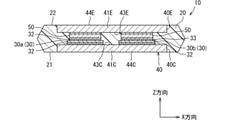
図7に示すように、X方向において配置が連続する3つ以上の主端子60により主端子群61が構成されている。上記したように主端子60C,60Eは隣り合って配置されており、主端子群61は主端子60C,60Eを両方含み、且つ、主端子60C,60Eの少なくとも一方を複数含んで構成されている。主端子群61を構成する主端子60は、それぞれの少なくとも一部が所定の領域A1内に配置されている。領域A1は、X方向において、IGBT30の一方の端面36から仮想的に延長された延長線L1と、端面36とは反対の端面37から仮想的に延長された延長線L2との間の領域である。X方向において、延長線L1,L2間の長さは、IGBT30の幅、すなわち素子幅に一致する。
As shown in FIG. 7, the main
本実施形態では、主端子60C,60Eが、その全長において同じ方向(Y方向)に延設されている。主端子60は、平面一直線状をなし、X方向への延設部分を有してない。主端子60Cの厚みは、本体部41Cよりも薄くされており、たとえば延設部42Cとほぼ同じとされている。主端子60Eの厚みは、本体部41Eよりも薄くされており、たとえば延設部42Eとほぼ同じとされている。主端子60の厚みは全長でほぼ一定とされており、主端子60C,60Eでほぼ同じ厚みとされている。主端子60の幅W1は全長でほぼ一定とされており、主端子60C,60Eで同じ幅とされている。また、X方向において隣り合う主端子60の間隔P1も、すべての主端子60で同じとされている。間隔P1は、端子間ピッチとも称される。
In this embodiment, the
主端子60のそれぞれは、封止樹脂体20内に屈曲部を2箇所有している。これにより、主端子60はZY平面において略クランク状をなしている。主端子60において、上記した屈曲部よりも先端の部分は平板状をなしており、この平板状部分の一部が、封止樹脂体20から突出している。封止樹脂体20からの突出部分、すなわち上記した平板状部分において、主端子60C,60Eは、図3及び図4に示すように、Z方向においてほぼ同じ位置に配置されている。また、平板状部分において、主端子60C,60Eの板厚方向は、Z方向に略一致している。これにより、主端子60Cの側面と主端子60Eの側面が、Z方向のほぼ全域で対向している。さらに、主端子60C,60Eの平板状部分の延設長さがほぼ同じであり、Y方向においてほぼ同じ位置に配置されている。これにより、主端子60C,60Eの側面は、平板状部分においてほぼ全面で対向している。
Each of the
図2,図5~図7に示すように、半導体装置10は、奇数本の主端子60、具体的には9本の主端子60を備えている。うち4本が主端子60C、残りの5本が主端子60Eとなっている。主端子60C,60EはX方向において交互に配置されており、これにより半導体装置10は、側面対向部を8つ有している。X方向両端には主端子60Eが配置されており、両端の主端子60Eを除く7本の主端子60により、主端子群61が構成されている。主端子群61は、奇数本(7本)の主端子60、具体的には4本の主端子60Cと3本の主端子60Eによって構成されている。主端子群61を構成しない2本の主端子60Eは、それぞれの全体がX方向において領域Aの外に配置されている。主端子群61を構成する主端子60のほうが、主端子群61を構成しない主端子60よりも多い構成となっている。
As shown in FIGS. 2, 5 to 7, the
主端子群61を構成する7本の主端子60のうち、両端に位置する2本の主端子60Cは、X方向においてそれぞれの一部が領域A1内に配置されている。残りの5本の主端子60は、X方向においてそれぞれの全体が領域A1内に配置されている。このように、主端子群61を構成する一部の主端子60は、それぞれの全体が領域A1内に配置され、残りの主端子60は、それぞれの一部が領域A1内に配置されている。特に本実施形態では、主端子群61を構成する複数(5本)の主端子60それぞれの全体が領域A1内に配置されている。
Of the seven
上記したように、主端子60C,60Eは同じ幅W1とされており、主端子60C,60Eの間隔P1も、すべての主端子60で同じとされている。そして、奇数本の主端子60のうち、X方向において真ん中(中央)に配置された主端子60Eにおける幅の中心が、IGBT30の中心を通る中心線CL上に位置している。このように、主端子60C、60Eは、X方向において、IGBT30の中心を通る中心線CLに対して線対称配置とされている。なお、複数の主端子60Cは中心線CLに対して線対称配置とされ、複数の主端子60Eは中心線CLに対して線対称配置とされている。また、主端子群61を構成する奇数本の主端子60も、中心線CLに対して線対称配置とされている。中心線CLの延設方向は、Z方向及びX方向に直交している。
As described above, the
(半導体装置の効果)
上記したように、本実施形態の半導体装置10は、主端子60C,60Eの少なくとも一方を複数有しており、主端子60C,60EがX方向において隣り合って配置されている。そして、隣り合う主端子60C,60Eの側面同士が対向している。主端子60C,60Eで主電流の向きは逆向きとなる。このように、主端子60C,60Eは、主電流が流れたときに生じる磁束をお互いに打ち消すように配置されている。したがって、インダクタンスを低減することができる。特に本実施形態では、主端子60C,60Eの側面対向部を複数有するため、インダクタンスを効果的に低減することができる。同じ種類の主端子60を複数にして並列化するため、インダクタンスを低減することができる。
(Effect of semiconductor device)
As described above, the
また、連続して配置された少なくとも3本の主端子60によって主端子群61が構成されている。主端子群61を構成する主端子60は、それぞれの少なくとも一部が、X方向において、IGBT30の両端面36,37から延長された延長線L1,L2間の領域A1内に配置されている。すなわち、複数の側面対向部が領域A1内に配置されている。これにより、主端子群61を構成する主端子60とIGBT30の主電極との電流経路を簡素化、具体的には電流経路を短くすることができる。したがって、インダクタンスを低減することができる。
Further, the main
以上により、本実施形態の半導体装置10によれば、従来よりも主回路配線のインダクタンスを低減することができる。なお、側面同士が対向するように複数の主端子60がX方向に並んで配置され、主端子60C,60Eの少なくとも一方を複数有し、少なくとも3本の主端子60により主端子群61が構成され、一部分において同じ種類の主端子60が連続して配置されるようにしてもよい。これによれば、主端子60C,60Eの少なくとも一方を複数にして並列化するため、インダクタンスを低減することができる。また、主端子群61を有することで、主端子群61を構成する主端子60とIGBT30の主電極との電流経路を簡素化することができる。これにより、インダクタンスを低減することができる。したがって、本実施形態に準ずる効果を奏することができる。しかしながら、本実施形態に示したように、主端子60C,60Eを隣り合うように配置したほうが、磁束打消しの効果によってインダクタンスをさらに低減することができる。
As described above, according to the
主端子群61において、X方向において全体が領域A1内に配置される主端子60のほうが、一部のみが領域A1に配置される主端子60よりも、電流経路の簡素化の点ではより好ましい。本実施形態では、主端子群61を構成する主端子60の一部についてそれぞれの全体が領域A1内に配置され、残りの主端子60についてそれぞれの一部が領域A1内に配置されている。主端子群61が、電流経路の簡素化についてより効果的な主端子60を含むため、インダクタンスを効果的に低減することができる。特に本実施形態では、全体が領域内に配置される主端子60を複数含んでいる。電流経路の簡素化についてより効果的な主端子60を複数含むため、インダクタンスをより効果的に低減することができる。
In the main
本実施形態では、主端子60の本数が奇数とされている。奇数の場合、X方向において対称性を取りやすく、主端子60とのIGBT30との電流経路の偏りを抑制することができる。また、X方向における主端子60の並び順が、一面21側から見ても、裏面22側から見ても同じである。したがって、半導体装置10の配置の自由度を向上することができる。
In this embodiment, the number of
特に本実施形態では、主端子60C,60Eは、X方向において、IGBT30の中心線CLに対して線対称配置とされている。これにより、IGBT30の主電流は、中心線CLに対して線対称となるように流れる。主電流は、中心線CLの左右でほぼ均等に流れる。したがって、インダクタンスをさらに低減することができる。また局所的な発熱を抑制することができる。
In particular, in the present embodiment, the
本実施形態では、奇数本の主端子60として9本の例を示したが、これに限定されない。たとえば図8~図10に示す変形例のように構成してもよい。図8~図10では、便宜上、封止樹脂体20及び信号端子70を省略して図示している。図8~図10では、便宜上、領域A1の図示を省略し、領域A1を規定する延長線L1,L2を示している。
In the present embodiment, nine examples are shown as the odd number of
図8に示す第1変形例では、半導体装置10が3本の主端子60、具体的には、1本の主端子60Cと2本の主端子60Eを備えている。すなわち、2つの側面対向部を有している。そして、すべての主端子60によって主端子群61が構成されている。真ん中に配置された主端子60Cは、X方向において全体が上記した領域A1に配置され、両端の主端子60Eは、それぞれの一部が領域A1に配置されている。
In the first modification shown in FIG. 8, the
図9に示す第2変形例では、半導体装置10が5本の主端子60、具体的には、2本の主端子60Cと3本の主端子60Eを備えている。すなわち、4つの側面対向部を有している。そして、すべての主端子60によって主端子群61が構成されている。両端の主端子60Eは、それぞれの一部が領域A1に配置され、残り3本の主端子60はそれぞれの全体が領域A1に配置されている。
In the second modification shown in FIG. 9, the
図10に示す第3変形例では、半導体装置10が7本の主端子60、具体的には、3本の主端子60Cと4本の主端子60Eを備えている。すなわち、6つの側面対向部を有している。そして、すべての主端子60によって主端子群61が構成されている。両端の主端子60Eは、それぞれの一部が領域A1に配置され、残り5本の主端子60はそれぞれの全体が領域A1に配置されている。
In the third modification shown in FIG. 10, the
図11は、半導体装置10が備える主端子トータルのインダクタンスについて磁場解析を行った結果を示している。この磁場解析(シミュレーション)では、導電部材40のX方向の長さ(幅)を17mm、主端子60の間隔P1を1.0mmとした。また、同じ半導体装置10を構成する主端子60において、幅W1を互いに等しいものとした。たとえば主端子60を3本有する構成の場合、図11では3端子と示している。図11では、比較例として主端子を2本のみ有する構成(2端子)を示している。9端子は、本実施形態に示した構成(図7参照)と同じ配置の結果を示している。同様に、3端子、5端子、7端子は、それぞれ第1変形例(図8参照)、第2変形例(図9参照)、第3変形例(図10参照)に示した構成と同じ配置の結果である。
FIG. 11 shows the result of magnetic field analysis on the total inductance of the main terminals included in the
端子数が増えるほど、1本当たりの幅は狭くなり、インダクタンス(自己インダクタンス)は増加する。しかしながら、側面対向部が増加し、主端子群61を構成する主端子60の本数も、所定の端子数までは端子数が増えるほど増加するため、インダクタンスを低減できる。3端子、5端子、及び7端子は、図8~図10に示したように、すべての主端子60によって主端子群61が構成されている。すなわち、すべての主端子60が領域A1内に配置されている。また、9端子は、図7に示したように、7本の主端子60によって主端子群61が構成されている。
As the number of terminals increases, the width per terminal becomes narrower and the inductance (self-inductance) increases. However, the number of side facing portions increases, and the number of
図11の結果から、3本以上の主端子60により構成される主端子群61を備えることで、体格の増大を抑制しつつ、比較例に較べて主端子トータルのインダクタンスを低減できることが明らかである。3端子以上では、上記したインダクタンス低減の効果が幅減少によるインダクタンス増加を上回り、インダクタンスが低減するためであると考えられる。特に5本以上の主端子60による主端子群61を備える構成とすると、比較例に較べてインダクタンスを半減以下にできる、すなわちインダクタンス低減に効果的であることが明らかである。
From the results of FIG. 11, it is clear that by providing the main
なお、9端子は、上記したように主端子群61を構成する7本の主端子60と、領域A1の外に配置された2本の主端子60を備えている。このように2本の主端子60が領域A1外とされてはいるものの、主端子群61を構成しない主端子60よりも多い主端子60、すなわち大部分の主端子60が領域A1に配置されている。また、側面対向部の数も7端子に較べて側面対向部が2つ多い。よって、7端子よりも低いインダクタンスを示している。
The 9 terminals include seven
上記した実施形態及び変形例では、主端子60Eが両端に配置される構成、すなわち主端子60Eのほうが主端子60Cよりも多い構成の例を示したがこれに限定されない。奇数本の主端子60において、主端子60Cを主端子60Eよりも多い構成としてもよい。
In the above-described embodiment and modification, an example of a configuration in which the
すべての主端子60において、封止樹脂体20からの突出部分の長さが等しい例を示したが、これに限定されない。バスバーなどとの接続性を考慮し、隣り合う主端子60C,60Eで突出部分の長さを異ならせてもよい。たとえば図12に示す第4変形例では、主端子60Cを主端子60Eよりも長くしている。
An example is shown in which the lengths of the protruding portions from the sealing
図13に示す第5変形例では、本数が少ない主端子60Cの断面積を、本数が多い主端子60Eの断面積よりも大きくし、これにより、主端子60Cトータルと主端子60Eトータルのインピーダンスをほぼ一致させている。したがって、本数が少ない主端子60Cの発熱を抑制することができる。図13では、幅を広くすることにより主端子60Cの断面積を主端子60Eの断面積よりも大きくしているが、主端子60Cの厚みを主端子60Eよりも厚くしてもよい。また、幅と厚みの両方を調整してもよい。図13では、本数が少ない主端子60Cの延設方向の長さを、主端子60Eの延設方向の長さよりも長くしている。長いほうが断面積が大きいため、主端子60の剛性を確保することができる。図12及び図13では7端子の例を示しているが、これに限定されるものではない。
In the fifth modification shown in FIG. 13, the cross-sectional area of the
封止樹脂体20からの突出部分において、延設方向の全長で隣り合う主端子60C,60Eが対向する例を示したが、これに限定されない。突出部分の一部で、側面同士が対向しない構成としてもよい。たとえば主端子60C,60Eの少なくとも一方において、突出先端部分が屈曲しており、これにより突出先端部分で対向しない構成としてもよい。延設長さが等しくても、バスバーなどとの接続性を高めることができる。しかしながら、インダクタンス低減の効果は減少する。
An example is shown in which the
主端子60の本数が奇数において、主端子群61を構成する主端子60の本数も奇数の例を示したが、これに限定されない。主端子群61を、偶数本(4本以上)の主端子60により構成してもよい。
Although the number of
半導体装置10は、少なくとも1つのIGBT30を備えればよい。たとえば複数のIGBT30を備え、これらIGBT30が主端子60C,60Eの間で互いに並列接続される構成において、各IGBT30に対して上記した主端子60の配置を適用してもよい。
The
図14に示す第6変形例のように、主端子群61を構成するすべての主端子60それぞれの全体が領域A1内に配置されてもよい。IGBT30の主電極との間の電流経路をより簡素化できる。図14では、7本の主端子60のうち、5本の主端子60によって主端子群61が構成されている。そして、主端子群61を構成する5本の主端子60は、それぞれの全体が領域A1内に配置されている。
As in the sixth modification shown in FIG. 14, the entire
(第2実施形態)
本実施形態は、先行実施形態を参照できる。このため、先行実施形態に示した半導体装置10と共通する部分についての説明は省略する。
(Second Embodiment)
This embodiment can refer to the preceding embodiment. Therefore, the description of the parts common to the
先行実施形態では、半導体装置10が奇数本(3本以上)の主端子60を備える例を示した。これに対し、本実施形態の半導体装置10は、偶数本(4本以上)の主端子60を備えている。それ以外の構成は、先行実施形態と同じである。
In the prior embodiment, an example is shown in which the
図15に示す例では、半導体装置10が4本の主端子60、具体的には主端子60C,60Eを2本ずつ備えている。主端子60Cと主端子60Eは交互に配置されている。4本の主端子60は、幅W1及び厚みのそれぞれが互いに等しくされている。すなわち、延設方向に直交する断面積が互いに等しくされている。また、Y方向の延設長さも、4本の主端子60で互いに等しくされている。
In the example shown in FIG. 15, the
また、すべての主端子60により主端子群61が構成されている。両端に配置された2本の主端子60C,60Eは、X方向においてそれぞれの一部が領域A1内に配置されている。真ん中の2本の主端子60C,60Eは、X方向においてそれぞれの全体が領域A1内に配置されている。
Further, the main
このように構成される半導体装置10によっても、先行実施形態に準ずる効果を奏することができる。具体的には、主端子60C,60Eの側面対向部を複数有するため、インダクタンスを効果的に低減することができる。また、主端子群61を有するため、主端子群61を構成する主端子60とIGBT30の主電極との電流経路を簡素化し、インダクタンスを低減することができる。以上により、従来よりも主回路配線のインダクタンスを低減することができる。図11には、4端子の結果も示している。図11の結果から、4端子の場合でも、体格の増大を抑制しつつ、比較例に較べて主端子トータルのインダクタンスを低減できることが明らかである。
Even with the
本実施形態では、すべての主端子60によって主端子群61が構成されているため、インダクタンスを効果的に低減することができる。なお、主端子60の本数が偶数の場合にも、連続して配置された3本以上の主端子60によって主端子群61が構成されればよい。したがって、4本の主端子60を備える構成において、3本により主端子群61が構成され、残りの1本が領域A1の外に配置された構成としてもよい。このように、主端子60の本数が偶数において、主端子群61を、奇数本(3本以上)の主端子60により構成してもよい。
In the present embodiment, since the main
本実施形態では、主端子60の本数が偶数であり、主端子60Cと主端子60Eとが同じ本数であるため、主端子60Cと主端子60Eとで流れる主電流が均等となり、これにより発熱のばらつきを抑制することができる。特に本実施形態では、主端子60C,60Eの延設長さが等しく、且つ、断面積も等しくされており、これにより、主端子60Cと主端子60Eのインピーダンスがほぼ等しくなっている。したがって、発熱ばらつきを効果的に抑制することができる。
In the present embodiment, the number of
主端子60の本数として4本の例を示したが、これに限定されない。4本以上の偶数であればよい。たとえば6本の主端子60を備える構成、8本の主端子60を備える構成としてもよい。
Although four examples are shown as the number of
先行実施形態の第4変形例、第5変形例で示したように、隣り合う主端子60C,60Eで突出部分の長さを異ならせてもよい。また、主端子60C,60Eのうち、突出部分の長さが長いほうの断面積を、短いほうの断面積よりも大きくしてもよい。これにより剛性を確保することができる。また、主端子60Cと主端子60Eとでインピーダンスを揃えることができる。先行実施形態に記載のように、突出部分の一部で、側面同士が対向しない構成としてもよい。
As shown in the fourth modification and the fifth modification of the preceding embodiment, the lengths of the protruding portions may be different between the adjacent
(第3実施形態)
本実施形態は、先行実施形態を参照できる。このため、先行実施形態に示した半導体装置10と共通する部分についての説明は省略する。
(Third Embodiment)
This embodiment can refer to the preceding embodiment. Therefore, the description of the parts common to the
本実施形態では、リードフレームの一部として、主端子60C,60Eの少なくとも一方とともに設けられた連結部をさらに備え、連結部によって、主端子60C,60Eの少なくとも一方において、同じ主端子同士が連結されている。
In the present embodiment, as a part of the lead frame, a connecting portion provided together with at least one of the
図16に示す例では、半導体装置10が5本の主端子60、具体的には2本の主端子60Cと3本の主端子60Eを備えている。また、上記したリードフレーム90が、主端子60E同士を連結する連結部86を有している。封止樹脂体20からの突出長さは、主端子60Eのほうが主端子60Cよりも長くされており、連結部86は主端子60Eの突出先端部分を連結している。連結部86はX方向に延設されており、Y方向において主端子60Cとは離れて設けられている。連結部86は、Z方向において主端子60C,60Eの突出部分と同じ位置に配置されている。
In the example shown in FIG. 16, the
このように、連結部86によって同電位の主端子60(主端子60E)を連結すると、バスバーなどとの接続点を減らすことができる。すなわち、接続性を向上することができる。特に図16では、本数の多い主端子60Eを連結している。これによれば、同一のリードフレーム90に主端子60C,60E及び連結部86を備える構成において、接続点をより少なくすることができる。
By connecting the main terminals 60 (
なお、主端子60Eに代えて、主端子60Cを連結部86にて連結してもよい。主端子60C,60Eのうち、本数の少ないほうを連結してもよい。主端子60の本数及び配置は図16に示す例に限定されない。主端子60C,60Eの一方のみに連結部86を設ける場合、連結部86を上記したように主端子60C,60Eの突出分と同一平面に設けることもできる。偶数本の主端子60を備える構成と組み合わせてもよい。
Instead of the
また、主端子60C,60Eのそれぞれを連結部にて連結してもよい。図17及び図18に示す第7変形例では、導電部材40C,40Eが本体部41C,41Eを有し、延設部42C,42Eを有していない。そして、同一のリードフレームに、導電部材40C、主端子60C、及び信号端子70が構成されている。また、主端子60Cを含むリードフレームとは別のリードフレームに、導電部材40E及び主端子60Eが構成されている。主端子60C,60Eは対応する導電部材40C,40Eから延設されている。図18は、図17のXVIII-XVIIIに沿う半導体装置10の断面図である。
Further, each of the
第7変形例では、主端子60C側のリードフレームに連結部86Cが設けられ、主端子60E側のリードフレームに連結部86Eが設けられている。そして、連結部86Cにより、突出先端部にて主端子60C同士が連結されている。また、連結部86Eにより、突出先端部にて主端子60E同士が連結されている。主端子60C,60Eは突出部分に屈曲部を有しており、これにより連結部86C,86EがZ方向において離反している。すなわち、連結部86C,86Eは、Z方向において互いに異なる位置に配置されている。したがって、延設長さが同じでも、主端子60C,60Eのそれぞれを連結部86C,86Eにて連結することができる。そして、接続点数をさらに少なくすることができる。
In the seventh modification, the connecting
(第4実施形態)
本実施形態は、先行実施形態を参照できる。このため、先行実施形態に示した半導体装置10と共通する部分についての説明は省略する。
(Fourth Embodiment)
This embodiment can refer to the preceding embodiment. Therefore, the description of the parts common to the
本実施形態の半導体装置10は、複数のIGBT30を備え、これらIGBT30は主端子60C,60Eの間で互いに並列接続されている。すなわち、1つのアームが並列接続された複数のIGBT30によって構成されている。図19及び図20に示す例では、半導体装置10が、IGBT30として、第1半導体素子に相当するIGBT30aと、第2半導体素子に相当するIGBT30bを備えている。なお、図19は、図20に示すXIX-XIX線に対応する半導体装置10の断面図である。
The
IGBT30a,30bのコレクタ電極32は、同じ導電部材40Cの実装面43Cに接続されている。また、IGBT30a,30bのエミッタ電極33は、個別に配置されたターミナル50を介して、同じ導電部材40Eの実装面43Eに接続されている。本実施形態では、2つのIGBT30a,30bが、互いにほぼ同じ平面形状、具体的には平面略矩形状をなすとともに、互いにほぼ同じ大きさとほぼ同じ厚みを有している。IGBT30a,30bは、Z方向においてほぼ同じ高さに位置するとともに、X方向において横並びで配置されている。
The
本実施形態では、X方向において配置が連続する2本以上の主端子60によって主端子群62が構成されている。半導体装置10は、主端子群62として、IGBT30aに対応する主端子群62aと、IGBT30bに対応する主端子群62bを有している。主端子群62aが第1群に相当し、主端子群62bが第2群に相当する。
In the present embodiment, the main
主端子群62aを構成する主端子60それぞれの少なくとも一部が、X方向において、IGBT30aの両端面36a,37aから延長された延長線L1a,L2a間の領域A1a内に配置されている。また、主端子群62bを構成する主端子60それぞれの少なくとも一部が、X方向において、IGBT30bの両端面36b,37bから延長された延長線L1b,L2b間の領域A1b内に配置されている。
At least a part of each of the
図19及び図20に示す例では、半導体装置10が5本の主端子60を備えている。具体的には、2本の主端子60Cと3本の主端子60Eを備えている。主端子60の幅W1及び厚みは互いに等しく、間隔P1もすべて等しくされている。そして、真ん中の主端子60Eが領域A1a,A1bの外に配置されている。X方向において真ん中の主端子60EよりもIGBT30a側に配置された2本の主端子60C,60Eにより主端子群62aが構成され、真ん中の主端子60EよりもIGBT30b側に配置された2本の主端子60C,60Eにより主端子群62bが構成されている。
In the example shown in FIGS. 19 and 20, the
さらに、主端子群62aを構成する主端子60C,60Eはそれぞれの全体が領域A1aに配置されている。同じく、主端子群62bを構成する主端子60C,60Eはそれぞれの全体が領域A1bに配置されている。そして、2つのIGBT30の素子的中心を通る中心線CLmに対して、5本の主端子60が線対称配置とされている。素子的中心とは、IGBT30a,30bの並び方向において中心間の中央位置であり、中心線CLmは、並び方向に直交し、素子的中心を通る仮想線である。
Further, the
本実施形態では、複数のIGBT30が並列接続された半導体装置10において、主端子60Cと主端子60Eとが交互に配置されている。そして、隣り合う主端子60C,60Eの側面同士が対向している。このように、主端子60Cと主端子60Eとの側面対向部を複数、具体的には4つ有するため、インダクタンスを効果的に低減することができる。
In the present embodiment, in the
また、主端子群62aを構成する主端子60C,60Eそれぞれの少なくとも一部が、領域A1a内に配置されている。したがって、主端子群62aを構成する主端子60C,60EとIGBT30aの主電極との電流経路を簡素化し、これによりインダクタンスを低減することができる。同じく、主端子群62bを構成する主端子60C,60Eそれぞれの少なくとも一部が領域A1b内に配置されている。したがって、主端子群62bを構成する主端子60C,60EとIGBT30bの主電極との電流経路を簡素化し、これによりインダクタンスを低減することができる。
Further, at least a part of each of the
以上により、本実施形態の半導体装置10によれば、従来よりも主回路配線のインダクタンスを低減することができる。
As described above, according to the
特に本実施形態では奇数本の主端子60が、2つのIGBT30の中心線CLmに対して線対称配置とされている。換言すれば、側面対向部が線対称配置とされている。したがって、IGBT30a,30bの主電流は、中心線CLmに対して線対称となるように流れる。すなわち、IGBT30a側のインダクタンスと、IGBT30b側のインダクタンスがほぼ等しくなっている。このように、インダクタンスを揃えることで、電流アンバランスを抑制することができる。
In particular, in the present embodiment, the odd number of
なお、2つのIGBT30が並列接続される例を示したが、これに限定されない。3つ以上のIGBT30が並列接続される構成にも適用できる。
Although an example in which two
主端子60の本数は上記例に限定されない。主端子群62のそれぞれが、主端子60C,60Eを含む2本以上の主端子60により構成されればよい。たとえば、7本の主端子60を備え、3本ずつの主端子60によって主端子群62a,62bが構成されてもよい。
The number of
第3実施形態に示した連結部86(86C,86E)を本実施形態に示した構成に組み合わせてもよい。 The connecting portion 86 (86C, 86E) shown in the third embodiment may be combined with the configuration shown in the present embodiment.
この明細書の開示は、例示された実施形態に制限されない。開示は、例示された実施形態と、それらに基づく当業者による変形態様を包含する。たとえば、開示は、実施形態において示された要素の組み合わせに限定されない。開示は、多様な組み合わせによって実施可能である。開示される技術的範囲は、実施形態の記載に限定されない。開示されるいくつかの技術的範囲は、特許請求の範囲の記載によって示され、さらに特許請求の範囲の記載と均等の意味及び範囲内でのすべての変更を含むものと解されるべきである。 The disclosure of this specification is not limited to the exemplified embodiments. Disclosures include exemplary embodiments and modifications by those skilled in the art based on them. For example, the disclosure is not limited to the combination of elements shown in the embodiments. Disclosure can be carried out in various combinations. The technical scope disclosed is not limited to the description of the embodiments. Some technical scopes disclosed are indicated by the description of the scope of claims and should be understood to include all modifications within the meaning and scope equivalent to the description of the scope of claims. ..
半導体装置10をインバータ5に適用する例を示したが、これに限定されない。たとえば昇圧コンバータに適用することもできる。また、インバータ5及び昇圧コンバータの両方に適用することもできる。
An example of applying the
IGBT30と一体的にFWD35が形成される例を示したが、これに限定されない。FWD35を別チップとしてもよい。
An example is shown in which the
半導体素子としてIGBT30の例を示したが、これに限定されない。たとえばMOSFETを採用することもできる。
Although an example of the
両面放熱構造の半導体装置10として、ターミナル50を備える例を示したが、これに限定されない。ターミナル50を備えない構成としてもよい。たとえば、ターミナル50の代わりに、導電部材40Eに、エミッタ電極33に向けて突出する凸部を設けてもよい。
An example in which the terminal 50 is provided as the
放熱面44C,44Eが、封止樹脂体20から露出される例を示したが、封止樹脂体20から露出されない構成としてもよい。たとえば図示しない絶縁部材によって放熱面44C,44Eを覆ってもよい。絶縁部材を放熱面44C,44Eに貼り合わせた状態で、封止樹脂体20を成形してもよい。
Although the example in which the
1…電力変換装置、2…直流電源、3…モータ、4…平滑コンデンサ、5…インバータ、6…高電位電源ライン、7…低電位電源ライン、8…出力ライン、10…半導体装置、20…封止樹脂体、21…一面、22…裏面、23,24…側面、30,30a,30b…IGBT、31…ゲート電極、32…コレクタ電極、33…エミッタ電極、34…パッド、35…FWD、36,37…端面、40,40C,40E…導電部材、41C,41E…本体部、42C,42E…延設部、43C,43E…実装面、44C,44E…放熱面、50…ターミナル、60,60C,60E…主端子、61,62,62a,62b…主端子群、70…信号端子、80~84…はんだ、85…ボンディングワイヤ、86,86C,86E…連結部、90…リードフレーム、91…外周枠部、92…タイバー 1 ... Power converter, 2 ... DC power supply, 3 ... Motor, 4 ... Smoothing capacitor, 5 ... Inverter, 6 ... High potential power supply line, 7 ... Low potential power supply line, 8 ... Output line, 10 ... Semiconductor device, 20 ... Encapsulating resin body, 21 ... one side, 22 ... back side, 23, 24 ... side surface, 30, 30a, 30b ... IGBT, 31 ... gate electrode, 32 ... collector electrode, 33 ... emitter electrode, 34 ... pad, 35 ... FWD, 36, 37 ... end face, 40, 40C, 40E ... conductive member, 41C, 41E ... main body, 42C, 42E ... extension, 43C, 43E ... mounting surface, 44C, 44E ... heat dissipation surface, 50 ... terminal, 60, 60C, 60E ... Main terminal, 61, 62, 62a, 62b ... Main terminal group, 70 ... Signal terminal, 80-84 ... Solder, 85 ... Bonding wire, 86, 86C, 86E ... Connecting part, 90 ... Lead frame, 91 … Outer frame, 92… Tie bar
Claims (14)
第1主電極(32)と、前記第1主電極との間に主電流が流れる第2主電極(33)と、を有する少なくとも1つの半導体素子(30)と、
前記第1主電極に接続された第1主端子(60C)及び前記第2主電極に接続された第2主端子(60E)を有するとともに、前記第1主端子及び前記第2主端子の少なくとも一方を複数有し、前記第1主端子と前記第2主端子とが、前記半導体素子の厚み方向に直交する一方向において側面同士が対向するように隣り合って配置された主端子(60)と、
備え、
前記一方向において配置が連続する3つ以上の前記主端子により主端子群(61)が構成され、
前記主端子群を構成する前記主端子それぞれの少なくとも一部が、前記一方向において、前記半導体素子の両端面(36,37)から延長された延長線間の領域(A1)内に配置されている半導体装置。 A semiconductor device that constitutes one arm of an upper and lower arm circuit.
An at least one semiconductor device (30) having a first main electrode (32) and a second main electrode (33) through which a main current flows between the first main electrode.
It has a first main terminal (60C) connected to the first main electrode and a second main terminal (60E) connected to the second main electrode, and at least the first main terminal and the second main terminal. A main terminal (60) having a plurality of one and having the first main terminal and the second main terminal adjacent to each other so that the side surfaces face each other in one direction orthogonal to the thickness direction of the semiconductor element. When,
Prepare,
The main terminal group (61) is composed of three or more main terminals having a continuous arrangement in one direction.
At least a part of each of the main terminals constituting the main terminal group is arranged in a region (A1) between extension lines extended from both end faces (36, 37) of the semiconductor element in the one direction. Semiconductor devices.
前記連結部によって、前記第1主端子及び前記第2主端子のうちの少なくとも一方において、同じ前記主端子同士が連結されている請求項1~12いずれか1項に記載の半導体装置。 As a part of the lead frame, a connecting portion (86, 86C, 86E) provided together with at least one of the first main terminal and the second main terminal is further provided.
The semiconductor device according to any one of claims 1 to 12, wherein the same main terminals are connected to each other at at least one of the first main terminal and the second main terminal by the connecting portion .
第1主電極(32)及び前記第1主電極との間に主電流が流れる第2主電極(33)をそれぞれ有し、少なくとも第1半導体素子(30a)及び第2半導体素子(30b)を含む複数の半導体素子(30)と、
前記第1主電極に接続された第1主端子(60C)及び前記第2主電極に接続された第2主端子(60E)を有するとともに、前記第1主端子及び前記第2主端子をそれぞれ複数有し、前記第1主端子と前記第2主端子とが、前記半導体素子の厚み方向に直交する一方向において側面同士が対向するように交互に配置された主端子(60)と、備え、
前記第1半導体素子及び前記第2半導体素子は、前記一方向に並んで配置されるとともに、前記第1主端子及び前記第2主端子の間で互いに並列に接続されており、
前記一方向において配置が連続する2つ以上の前記主端子により構成された主端子群(62)として第1群(62a)及び第2群(62b)を有し、
前記第1群を構成する前記主端子それぞれの少なくとも一部が、前記一方向において、前記第1半導体素子の両端面(36a,37a)から延長された延長線間の領域(A1a)内に配置され、前記第2群を構成する前記主端子それぞれの少なくとも一部が、前記一方向において、前記第2半導体素子の両端面(36b,37b)から延長された延長線間の領域(A1b)内に配置され、
リードフレームの一部として、前記第1主端子及び前記第2主端子の少なくとも一方とともに設けられた連結部(86,86C,86E)をさらに備え、
前記連結部によって、前記第1主端子及び前記第2主端子のうちの少なくとも一方において、同じ前記主端子同士が連結されている半導体装置。 A semiconductor device that constitutes one arm of an upper and lower arm circuit.
It has a second main electrode (33) through which a main current flows between the first main electrode (32) and the first main electrode, respectively, and has at least a first semiconductor element (30a) and a second semiconductor element (30b). Multiple semiconductor devices (30) including
It has a first main terminal (60C) connected to the first main electrode and a second main terminal (60E) connected to the second main electrode, and has the first main terminal and the second main terminal, respectively. A plurality of main terminals (60) are provided, wherein the first main terminal and the second main terminal are alternately arranged so that the side surfaces face each other in one direction orthogonal to the thickness direction of the semiconductor element. ,
The first semiconductor element and the second semiconductor element are arranged side by side in the one direction, and are connected in parallel between the first main terminal and the second main terminal.
The main terminal group (62) composed of two or more main terminals having a continuous arrangement in one direction has a first group (62a) and a second group (62b).
At least a part of each of the main terminals constituting the first group is arranged in a region (A1a) between extension lines extended from both end faces (36a, 37a) of the first semiconductor element in the one direction. At least a part of each of the main terminals constituting the second group is in the region (A1b) between the extension lines extended from both end faces (36b, 37b) of the second semiconductor element in the one direction. Placed in
As a part of the lead frame, a connecting portion (86, 86C, 86E) provided together with at least one of the first main terminal and the second main terminal is further provided.
A semiconductor device in which the same main terminals are connected to each other at at least one of the first main terminal and the second main terminal by the connecting portion .
Priority Applications (5)
| Application Number | Priority Date | Filing Date | Title |
|---|---|---|---|
| JP2018139471A JP7010167B2 (en) | 2018-07-25 | 2018-07-25 | Semiconductor device |
| CN201980048810.5A CN112543994B (en) | 2018-07-25 | 2019-05-28 | Semiconductor device with a semiconductor device having a plurality of semiconductor chips |
| DE112019003733.1T DE112019003733T5 (en) | 2018-07-25 | 2019-05-28 | Semiconductor device |
| PCT/JP2019/021059 WO2020021843A1 (en) | 2018-07-25 | 2019-05-28 | Semiconductor device |
| US17/155,696 US11456238B2 (en) | 2018-07-25 | 2021-01-22 | Semiconductor device including a semiconductor chip connected with a plurality of main terminals |
Applications Claiming Priority (1)
| Application Number | Priority Date | Filing Date | Title |
|---|---|---|---|
| JP2018139471A JP7010167B2 (en) | 2018-07-25 | 2018-07-25 | Semiconductor device |
Publications (3)
| Publication Number | Publication Date |
|---|---|
| JP2020017623A JP2020017623A (en) | 2020-01-30 |
| JP2020017623A5 JP2020017623A5 (en) | 2020-07-30 |
| JP7010167B2 true JP7010167B2 (en) | 2022-01-26 |
Family
ID=69182241
Family Applications (1)
| Application Number | Title | Priority Date | Filing Date |
|---|---|---|---|
| JP2018139471A Active JP7010167B2 (en) | 2018-07-25 | 2018-07-25 | Semiconductor device |
Country Status (5)
| Country | Link |
|---|---|
| US (1) | US11456238B2 (en) |
| JP (1) | JP7010167B2 (en) |
| CN (1) | CN112543994B (en) |
| DE (1) | DE112019003733T5 (en) |
| WO (1) | WO2020021843A1 (en) |
Families Citing this family (6)
| Publication number | Priority date | Publication date | Assignee | Title |
|---|---|---|---|---|
| DE112019003699T5 (en) | 2018-07-25 | 2021-04-08 | Denso Corporation | Power module and electric power conversion device |
| JP6915633B2 (en) | 2018-07-25 | 2021-08-04 | 株式会社デンソー | Power converter |
| JP7034043B2 (en) * | 2018-09-28 | 2022-03-11 | 京セラ株式会社 | Power module and electrical equipment with power module |
| JP7059970B2 (en) * | 2019-03-11 | 2022-04-26 | 株式会社デンソー | Semiconductor device |
| JP7103279B2 (en) * | 2019-03-11 | 2022-07-20 | 株式会社デンソー | Semiconductor equipment |
| JP7095632B2 (en) * | 2019-03-11 | 2022-07-05 | 株式会社デンソー | Semiconductor equipment |
Citations (5)
| Publication number | Priority date | Publication date | Assignee | Title |
|---|---|---|---|---|
| JP2014050206A (en) | 2012-08-31 | 2014-03-17 | Hitachi Automotive Systems Ltd | Power semiconductor module |
| JP2014093421A (en) | 2012-11-02 | 2014-05-19 | Toyota Motor Corp | Power module |
| JP2015115464A (en) | 2013-12-11 | 2015-06-22 | トヨタ自動車株式会社 | Semiconductor device |
| JP2016226131A (en) | 2015-05-29 | 2016-12-28 | 日立オートモティブシステムズ株式会社 | Power semiconductor device |
| JP2018078184A (en) | 2016-11-09 | 2018-05-17 | トヨタ自動車株式会社 | Semiconductor device |
Family Cites Families (19)
| Publication number | Priority date | Publication date | Assignee | Title |
|---|---|---|---|---|
| US7095099B2 (en) | 2003-11-12 | 2006-08-22 | International Rectifier Corporation | Low profile package having multiple die |
| DE102005016830A1 (en) * | 2004-04-14 | 2005-11-03 | Denso Corp., Kariya | Semiconductor device and method for its production |
| JP4407489B2 (en) * | 2004-11-19 | 2010-02-03 | 株式会社デンソー | Semiconductor device manufacturing method and semiconductor device manufacturing apparatus |
| JP2007073743A (en) * | 2005-09-07 | 2007-03-22 | Denso Corp | Semiconductor device |
| US8497572B2 (en) * | 2010-07-05 | 2013-07-30 | Denso Corporation | Semiconductor module and method of manufacturing the same |
| JP5520889B2 (en) * | 2011-06-24 | 2014-06-11 | 日立オートモティブシステムズ株式会社 | Power semiconductor module and power converter using the same |
| JP5661052B2 (en) * | 2012-01-18 | 2015-01-28 | 三菱電機株式会社 | Power semiconductor module and manufacturing method thereof |
| JP6065771B2 (en) * | 2013-07-03 | 2017-01-25 | 株式会社デンソー | Semiconductor device |
| JP6221542B2 (en) * | 2013-09-16 | 2017-11-01 | 株式会社デンソー | Semiconductor device |
| JP6102676B2 (en) | 2013-10-23 | 2017-03-29 | 株式会社デンソー | Semiconductor device |
| JP6166701B2 (en) * | 2014-08-22 | 2017-07-19 | 株式会社東芝 | Semiconductor device |
| JP6344215B2 (en) * | 2014-11-21 | 2018-06-20 | 株式会社デンソー | Semiconductor device and power module |
| JP6256419B2 (en) * | 2015-06-24 | 2018-01-10 | 株式会社デンソー | Semiconductor chip and semiconductor module using the same |
| JP2017099140A (en) * | 2015-11-24 | 2017-06-01 | トヨタ自動車株式会社 | Power conversion device |
| JP6638477B2 (en) * | 2016-03-07 | 2020-01-29 | トヨタ自動車株式会社 | Semiconductor device |
| WO2017163583A1 (en) * | 2016-03-22 | 2017-09-28 | 富士電機株式会社 | Semiconductor device and method for manufacturing semiconductor device |
| JP6708066B2 (en) * | 2016-09-05 | 2020-06-10 | 株式会社デンソー | Semiconductor device |
| JP2019067949A (en) * | 2017-10-02 | 2019-04-25 | トヨタ自動車株式会社 | Semiconductor device |
| JP2019212833A (en) * | 2018-06-07 | 2019-12-12 | ルネサスエレクトロニクス株式会社 | Semiconductor device and manufacturing method thereof |
-
2018
- 2018-07-25 JP JP2018139471A patent/JP7010167B2/en active Active
-
2019
- 2019-05-28 CN CN201980048810.5A patent/CN112543994B/en active Active
- 2019-05-28 DE DE112019003733.1T patent/DE112019003733T5/en active Granted
- 2019-05-28 WO PCT/JP2019/021059 patent/WO2020021843A1/en active Application Filing
-
2021
- 2021-01-22 US US17/155,696 patent/US11456238B2/en active Active
Patent Citations (5)
| Publication number | Priority date | Publication date | Assignee | Title |
|---|---|---|---|---|
| JP2014050206A (en) | 2012-08-31 | 2014-03-17 | Hitachi Automotive Systems Ltd | Power semiconductor module |
| JP2014093421A (en) | 2012-11-02 | 2014-05-19 | Toyota Motor Corp | Power module |
| JP2015115464A (en) | 2013-12-11 | 2015-06-22 | トヨタ自動車株式会社 | Semiconductor device |
| JP2016226131A (en) | 2015-05-29 | 2016-12-28 | 日立オートモティブシステムズ株式会社 | Power semiconductor device |
| JP2018078184A (en) | 2016-11-09 | 2018-05-17 | トヨタ自動車株式会社 | Semiconductor device |
Also Published As
| Publication number | Publication date |
|---|---|
| WO2020021843A1 (en) | 2020-01-30 |
| CN112543994B (en) | 2023-10-17 |
| US20210143088A1 (en) | 2021-05-13 |
| JP2020017623A (en) | 2020-01-30 |
| US11456238B2 (en) | 2022-09-27 |
| DE112019003733T5 (en) | 2021-04-08 |
| CN112543994A (en) | 2021-03-23 |
Similar Documents
| Publication | Publication Date | Title |
|---|---|---|
| JP7010167B2 (en) | Semiconductor device | |
| JP6717270B2 (en) | Semiconductor module | |
| JP6394489B2 (en) | Semiconductor device | |
| JP6836201B2 (en) | Power converter | |
| JP6708066B2 (en) | Semiconductor device | |
| CN112166500B (en) | Semiconductor device with a semiconductor device having a plurality of semiconductor chips | |
| JP2018117048A (en) | Semiconductor device | |
| JP6610568B2 (en) | Semiconductor device | |
| US10535577B2 (en) | Semiconductor device | |
| US20210407875A1 (en) | Semiconductor device | |
| WO2023065602A1 (en) | Power module and motor controller | |
| US20210407881A1 (en) | Semiconductor device | |
| US20200211954A1 (en) | Semiconductor module | |
| US11887905B2 (en) | Semiconductor device | |
| JP6123722B2 (en) | Semiconductor device | |
| JP7192235B2 (en) | semiconductor equipment |
Legal Events
| Date | Code | Title | Description |
|---|---|---|---|
| A521 | Request for written amendment filed |
Free format text: JAPANESE INTERMEDIATE CODE: A523 Effective date: 20200601 |
|
| A621 | Written request for application examination |
Free format text: JAPANESE INTERMEDIATE CODE: A621 Effective date: 20200601 |
|
| A131 | Notification of reasons for refusal |
Free format text: JAPANESE INTERMEDIATE CODE: A131 Effective date: 20210817 |
|
| A521 | Request for written amendment filed |
Free format text: JAPANESE INTERMEDIATE CODE: A523 Effective date: 20211004 |
|
| TRDD | Decision of grant or rejection written | ||
| A01 | Written decision to grant a patent or to grant a registration (utility model) |
Free format text: JAPANESE INTERMEDIATE CODE: A01 Effective date: 20211214 |
|
| A61 | First payment of annual fees (during grant procedure) |
Free format text: JAPANESE INTERMEDIATE CODE: A61 Effective date: 20211227 |