JP7006517B2 - How to control the defect density in a silicon single crystal substrate - Google Patents
How to control the defect density in a silicon single crystal substrate Download PDFInfo
- Publication number
- JP7006517B2 JP7006517B2 JP2018112062A JP2018112062A JP7006517B2 JP 7006517 B2 JP7006517 B2 JP 7006517B2 JP 2018112062 A JP2018112062 A JP 2018112062A JP 2018112062 A JP2018112062 A JP 2018112062A JP 7006517 B2 JP7006517 B2 JP 7006517B2
- Authority
- JP
- Japan
- Prior art keywords
- single crystal
- silicon single
- crystal substrate
- defect density
- nitrogen concentration
- Prior art date
- Legal status (The legal status is an assumption and is not a legal conclusion. Google has not performed a legal analysis and makes no representation as to the accuracy of the status listed.)
- Active
Links
- XUIMIQQOPSSXEZ-UHFFFAOYSA-N Silicon Chemical compound [Si] XUIMIQQOPSSXEZ-UHFFFAOYSA-N 0.000 title claims description 192
- 229910052710 silicon Inorganic materials 0.000 title claims description 190
- 239000010703 silicon Substances 0.000 title claims description 190
- 239000013078 crystal Substances 0.000 title claims description 185
- 239000000758 substrate Substances 0.000 title claims description 160
- 230000007547 defect Effects 0.000 title claims description 106
- IJGRMHOSHXDMSA-UHFFFAOYSA-N Atomic nitrogen Chemical compound N#N IJGRMHOSHXDMSA-UHFFFAOYSA-N 0.000 claims description 218
- 229910052757 nitrogen Inorganic materials 0.000 claims description 112
- 238000000034 method Methods 0.000 claims description 78
- 229910052760 oxygen Inorganic materials 0.000 claims description 60
- QVGXLLKOCUKJST-UHFFFAOYSA-N atomic oxygen Chemical compound [O] QVGXLLKOCUKJST-UHFFFAOYSA-N 0.000 claims description 59
- 239000001301 oxygen Substances 0.000 claims description 59
- 238000010438 heat treatment Methods 0.000 claims description 56
- 238000010894 electron beam technology Methods 0.000 claims description 38
- 229910052799 carbon Inorganic materials 0.000 claims description 37
- OKTJSMMVPCPJKN-UHFFFAOYSA-N Carbon Chemical group [C] OKTJSMMVPCPJKN-UHFFFAOYSA-N 0.000 claims description 35
- 238000012360 testing method Methods 0.000 claims description 24
- 238000002796 luminescence method Methods 0.000 claims description 17
- 238000005424 photoluminescence Methods 0.000 claims description 15
- 238000005259 measurement Methods 0.000 claims description 14
- 230000001133 acceleration Effects 0.000 claims description 9
- 238000002360 preparation method Methods 0.000 claims description 9
- 238000004519 manufacturing process Methods 0.000 claims description 8
- 230000001678 irradiating effect Effects 0.000 claims description 6
- 239000002245 particle Substances 0.000 description 35
- 238000011084 recovery Methods 0.000 description 21
- 229910052720 vanadium Inorganic materials 0.000 description 15
- 230000006798 recombination Effects 0.000 description 14
- 238000005215 recombination Methods 0.000 description 14
- 239000002994 raw material Substances 0.000 description 12
- 125000004429 atom Chemical group 0.000 description 11
- 239000012535 impurity Substances 0.000 description 11
- 101001074449 Crotalus durissus terrificus Phospholipase A2 inhibitor CNF Proteins 0.000 description 7
- 239000004065 semiconductor Substances 0.000 description 7
- 101100060033 Drosophila melanogaster cic gene Proteins 0.000 description 6
- 101100060035 Mus musculus Cic gene Proteins 0.000 description 6
- 230000000052 comparative effect Effects 0.000 description 5
- 239000002019 doping agent Substances 0.000 description 5
- 238000000295 emission spectrum Methods 0.000 description 5
- 229910021420 polycrystalline silicon Inorganic materials 0.000 description 5
- 238000006243 chemical reaction Methods 0.000 description 4
- 239000002131 composite material Substances 0.000 description 4
- 230000007423 decrease Effects 0.000 description 4
- 239000000969 carrier Substances 0.000 description 3
- 229910052698 phosphorus Inorganic materials 0.000 description 3
- 239000011148 porous material Substances 0.000 description 3
- 230000004913 activation Effects 0.000 description 2
- 230000015572 biosynthetic process Effects 0.000 description 2
- 229910052796 boron Inorganic materials 0.000 description 2
- -1 can be observed Chemical compound 0.000 description 2
- 150000001721 carbon Chemical class 0.000 description 2
- 238000005136 cathodoluminescence Methods 0.000 description 2
- 238000005520 cutting process Methods 0.000 description 2
- 230000001419 dependent effect Effects 0.000 description 2
- 239000007789 gas Substances 0.000 description 2
- 239000001257 hydrogen Substances 0.000 description 2
- 229910052739 hydrogen Inorganic materials 0.000 description 2
- 125000004435 hydrogen atom Chemical class [H]* 0.000 description 2
- 238000004020 luminiscence type Methods 0.000 description 2
- 239000000463 material Substances 0.000 description 2
- 229910021421 monocrystalline silicon Inorganic materials 0.000 description 2
- 239000011574 phosphorus Substances 0.000 description 2
- 229920005591 polysilicon Polymers 0.000 description 2
- FSLGCYNKXXIWGJ-UHFFFAOYSA-N silicon(1+) Chemical compound [Si+] FSLGCYNKXXIWGJ-UHFFFAOYSA-N 0.000 description 2
- 239000000126 substance Substances 0.000 description 2
- ZOXJGFHDIHLPTG-UHFFFAOYSA-N Boron Chemical compound [B] ZOXJGFHDIHLPTG-UHFFFAOYSA-N 0.000 description 1
- OAICVXFJPJFONN-UHFFFAOYSA-N Phosphorus Chemical compound [P] OAICVXFJPJFONN-UHFFFAOYSA-N 0.000 description 1
- 229910052581 Si3N4 Inorganic materials 0.000 description 1
- 238000010521 absorption reaction Methods 0.000 description 1
- 150000001638 boron Chemical class 0.000 description 1
- 238000003486 chemical etching Methods 0.000 description 1
- 239000000470 constituent Substances 0.000 description 1
- 230000002950 deficient Effects 0.000 description 1
- 238000010586 diagram Methods 0.000 description 1
- 230000000694 effects Effects 0.000 description 1
- 238000011156 evaluation Methods 0.000 description 1
- 230000005284 excitation Effects 0.000 description 1
- 238000002474 experimental method Methods 0.000 description 1
- 230000005524 hole trap Effects 0.000 description 1
- 238000005468 ion implantation Methods 0.000 description 1
- 150000003017 phosphorus Chemical class 0.000 description 1
- 238000005498 polishing Methods 0.000 description 1
- 238000001004 secondary ion mass spectrometry Methods 0.000 description 1
- HQVNEWCFYHHQES-UHFFFAOYSA-N silicon nitride Chemical compound N12[Si]34N5[Si]62N3[Si]51N64 HQVNEWCFYHHQES-UHFFFAOYSA-N 0.000 description 1
Images


Classifications
-
- H—ELECTRICITY
- H01—ELECTRIC ELEMENTS
- H01L—SEMICONDUCTOR DEVICES NOT COVERED BY CLASS H10
- H01L21/00—Processes or apparatus adapted for the manufacture or treatment of semiconductor or solid state devices or of parts thereof
- H01L21/02—Manufacture or treatment of semiconductor devices or of parts thereof
- H01L21/04—Manufacture or treatment of semiconductor devices or of parts thereof the devices having potential barriers, e.g. a PN junction, depletion layer or carrier concentration layer
- H01L21/18—Manufacture or treatment of semiconductor devices or of parts thereof the devices having potential barriers, e.g. a PN junction, depletion layer or carrier concentration layer the devices having semiconductor bodies comprising elements of Group IV of the Periodic Table or AIIIBV compounds with or without impurities, e.g. doping materials
- H01L21/26—Bombardment with radiation
- H01L21/263—Bombardment with radiation with high-energy radiation
-
- C—CHEMISTRY; METALLURGY
- C30—CRYSTAL GROWTH
- C30B—SINGLE-CRYSTAL GROWTH; UNIDIRECTIONAL SOLIDIFICATION OF EUTECTIC MATERIAL OR UNIDIRECTIONAL DEMIXING OF EUTECTOID MATERIAL; REFINING BY ZONE-MELTING OF MATERIAL; PRODUCTION OF A HOMOGENEOUS POLYCRYSTALLINE MATERIAL WITH DEFINED STRUCTURE; SINGLE CRYSTALS OR HOMOGENEOUS POLYCRYSTALLINE MATERIAL WITH DEFINED STRUCTURE; AFTER-TREATMENT OF SINGLE CRYSTALS OR A HOMOGENEOUS POLYCRYSTALLINE MATERIAL WITH DEFINED STRUCTURE; APPARATUS THEREFOR
- C30B13/00—Single-crystal growth by zone-melting; Refining by zone-melting
-
- C—CHEMISTRY; METALLURGY
- C30—CRYSTAL GROWTH
- C30B—SINGLE-CRYSTAL GROWTH; UNIDIRECTIONAL SOLIDIFICATION OF EUTECTIC MATERIAL OR UNIDIRECTIONAL DEMIXING OF EUTECTOID MATERIAL; REFINING BY ZONE-MELTING OF MATERIAL; PRODUCTION OF A HOMOGENEOUS POLYCRYSTALLINE MATERIAL WITH DEFINED STRUCTURE; SINGLE CRYSTALS OR HOMOGENEOUS POLYCRYSTALLINE MATERIAL WITH DEFINED STRUCTURE; AFTER-TREATMENT OF SINGLE CRYSTALS OR A HOMOGENEOUS POLYCRYSTALLINE MATERIAL WITH DEFINED STRUCTURE; APPARATUS THEREFOR
- C30B29/00—Single crystals or homogeneous polycrystalline material with defined structure characterised by the material or by their shape
- C30B29/02—Elements
- C30B29/06—Silicon
-
- H—ELECTRICITY
- H01—ELECTRIC ELEMENTS
- H01L—SEMICONDUCTOR DEVICES NOT COVERED BY CLASS H10
- H01L22/00—Testing or measuring during manufacture or treatment; Reliability measurements, i.e. testing of parts without further processing to modify the parts as such; Structural arrangements therefor
- H01L22/10—Measuring as part of the manufacturing process
- H01L22/12—Measuring as part of the manufacturing process for structural parameters, e.g. thickness, line width, refractive index, temperature, warp, bond strength, defects, optical inspection, electrical measurement of structural dimensions, metallurgic measurement of diffusions
-
- H—ELECTRICITY
- H01—ELECTRIC ELEMENTS
- H01L—SEMICONDUCTOR DEVICES NOT COVERED BY CLASS H10
- H01L22/00—Testing or measuring during manufacture or treatment; Reliability measurements, i.e. testing of parts without further processing to modify the parts as such; Structural arrangements therefor
- H01L22/20—Sequence of activities consisting of a plurality of measurements, corrections, marking or sorting steps
Landscapes
- Engineering & Computer Science (AREA)
- Chemical & Material Sciences (AREA)
- Manufacturing & Machinery (AREA)
- Computer Hardware Design (AREA)
- Physics & Mathematics (AREA)
- Power Engineering (AREA)
- Microelectronics & Electronic Packaging (AREA)
- Materials Engineering (AREA)
- High Energy & Nuclear Physics (AREA)
- Crystallography & Structural Chemistry (AREA)
- Metallurgy (AREA)
- Organic Chemistry (AREA)
- Health & Medical Sciences (AREA)
- General Physics & Mathematics (AREA)
- Condensed Matter Physics & Semiconductors (AREA)
- Toxicology (AREA)
- Crystals, And After-Treatments Of Crystals (AREA)
- Testing Or Measuring Of Semiconductors Or The Like (AREA)
Description
本発明は、シリコン単結晶基板中の欠陥密度の制御方法に関する。 The present invention relates to a method for controlling the defect density in a silicon single crystal substrate.
シリコン単結晶基板を用いた半導体素子の製造工程では、粒子線照射と熱処理が頻繁に行われる。例えば、トランジスタのソース/ドレインの形成工程では、高濃度のドーパントをイオン注入し、その後の熱処理により、ドーパントを活性化させるとともに、イオン注入によって生じたダメージを回復させる。また、パワーデバイスにおける過剰キャリアの再結合ライフタイムを制御する工程では、電子線やプロトンなどの粒子線照射によりキャリアの再結合中心となる欠陥を故意に導入し、その後の熱処理により再結合ライフタイムの調整を行う。 In the manufacturing process of a semiconductor device using a silicon single crystal substrate, particle beam irradiation and heat treatment are frequently performed. For example, in the process of forming a source / drain of a transistor, a high-concentration dopant is ion-implanted, and the subsequent heat treatment activates the dopant and recovers the damage caused by the ion implantation. In addition, in the process of controlling the recombination lifetime of excess carriers in a power device, defects that are the center of carrier recombination are intentionally introduced by irradiation with particle beams such as electron beams and protons, and the recombination lifetime is performed by subsequent heat treatment. Make adjustments.
シリコン単結晶基板に対して、高エネルギーの粒子線を照射すると、格子位置のシリコン原子が弾き出されて、格子間シリコン(I)とその抜け殻である空孔(V)が生成される。過剰に生成されたIやVは、単体では不安定なため、再結合したり(V+I→0)、I同士やV同士がクラスタリングしたり、シリコン単結晶基板中に含まれる軽元素不純物と反応して複合体を形成する。そして、IやVのクラスターや、IやVと軽元素不純物の複合体は、シリコンのバンドギャップ中に深い準位を形成して、キャリアの再結合中心や発生中心として働く。これらの再結合中心や発生中心がデバイス特性を劣化させるような場合には、軽元素複合体の密度を、できる限り低くすることが望まれる。 When a silicon single crystal substrate is irradiated with a high-energy particle beam, silicon atoms at lattice positions are ejected to generate interstitial silicon (I) and pores (V) which are shells thereof. Excessively generated I and V are unstable by themselves, so they may recombine (V + I → 0), cluster I or V with each other, or react with light element impurities contained in the silicon single crystal substrate. To form a complex. The clusters of I and V and the complex of I and V and light element impurities form deep levels in the band gap of silicon and act as carriers recombination centers and generation centers. When these recombination centers and generation centers deteriorate the device characteristics, it is desirable to reduce the density of the light element complex as much as possible.
一方、IGBT(Insulated Gate Bipolor Transistor、絶縁ゲート型バイポーラトランジスタ)やダイオード等のパワーデバイスにおいては、粒子線照射と熱処理により、シリコン単結晶基板中にキャリアの再結合中心となる欠陥を意図的に導入して、キャリアの再結合ライフタイムを短く制御することによって、スイッチング速度を高速化し、結果的にスイッチング損失を低減させる技術が従来から用いられている(特許文献1~4)。この場合、粒子線照射により、複数種の、再結合中心となる欠陥が室温付近で導入され、その中には熱的に不安定な欠陥種も存在するため、粒子線照射後に熱処理を施すことで熱的に不安定な欠陥を消滅させ、欠陥密度を調整することにより、再結合ライフタイムの所望の値が得られるようにする。 On the other hand, in power devices such as IGBTs (Insulated Gate Bipolar Transistors) and diodes, defects that are the center of carrier recombination are intentionally introduced into the silicon single crystal substrate by particle beam irradiation and heat treatment. Therefore, techniques have been conventionally used in which the switching speed is increased by controlling the recombination lifetime of the carriers to be short, and as a result, the switching loss is reduced (Patent Documents 1 to 4). In this case, multiple types of defects that are the centers of recombination are introduced by particle beam irradiation near room temperature, and some of them are thermally unstable, so heat treatment should be performed after particle beam irradiation. The thermally unstable defects are eliminated and the defect density is adjusted so that the desired value of the recombination lifetime can be obtained.
しかしながら、粒子線照射の条件や、粒子線照射後の熱処理の条件を同じにしても、デバイス特性がばらつくという問題があった(非特許文献1~4)。デバイス特性のばらつき要因として、シリコン基板自体に含まれる何らかの物質が要因として疑われており、特に炭素や酸素の不純物の影響が懸念されている。 However, even if the conditions of particle beam irradiation and the conditions of heat treatment after particle beam irradiation are the same, there is a problem that the device characteristics vary (Non-Patent Documents 1 to 4). It is suspected that some substance contained in the silicon substrate itself is a factor that causes variation in device characteristics, and there is particular concern about the influence of impurities such as carbon and oxygen.
非特許文献1では、同じ再結合ライフタイム制御を行った場合でも、スイッチング損失にウェーハ依存が発生することがある問題を指摘し、電子線照射により生成する主要な欠陥(CsI、CiCs、又はCiOi)のうち、CiOiのみ活性化エネルギーにウェーハ依存性があり、酸素濃度が高い場合に活性化エネルギーが高くなる傾向があるため、酸素不純物がウェーハ依存の要因になると考えられる、としている(但し、Cs:置換型炭素、Ci:格子間型炭素、Oi:格子間型酸素、I:格子間シリコンである)。また、非特許文献2及び非特許文献3では、電子線照射後に350℃±10℃で熱処理した場合に、IGBTのON電圧であるVCE(sat)と、フォトルミネッセンス法で測定したCiOiに由来するC線発光強度に相関があることが示されている。また、非特許文献4では、FWD(Free Wheeling Diode)のリカバリー特性の改善において、He照射のようにドナー濃度と同等以上で局所的に結晶欠陥を導入する場合は、正孔トラップとして働くCiOiの密度制御が重要であり、ひいては炭素濃度制御が重要であることが記載されている。このような場合、軽元素複合体の密度は、できる限りばらつかないように制御する必要がある。 Non-Patent Document 1 points out the problem that wafer dependence may occur in switching loss even when the same recombination lifetime control is performed, and the main defects (CsI, CiCs, or CiOi) generated by electron beam irradiation are pointed out. ), Only CiOi has a wafer-dependent activation energy, and the activation energy tends to increase when the oxygen concentration is high. Therefore, oxygen impurities are considered to be a wafer-dependent factor (however,). Cs: substituted carbon, Ci: interstitial carbon, Oi: interstitial oxygen, I: interstitial silicon). Further, in Non-Patent Document 2 and Non-Patent Document 3, it is derived from VCE (sat) , which is the ON voltage of the IGBT, and CiOi measured by the photoluminescence method when heat-treated at 350 ° C. ± 10 ° C. after electron beam irradiation. It has been shown that there is a correlation with the C-ray emission intensity. Further, in Non-Patent Document 4, in improving the recovery characteristics of FWD (Free Holeing Diode), when crystal defects are locally introduced at a concentration equal to or higher than the donor concentration as in He irradiation, CiOi that acts as a hole trap is used. It is stated that density control is important, and thus carbon concentration control is important. In such cases, the density of the light element complex needs to be controlled so as not to vary as much as possible.
前述のように、デバイス特性を向上させるためには、粒子線照射と熱処理により形成される軽元素複合体の密度をより厳密に制御する必要がある。 As mentioned above, in order to improve the device characteristics, it is necessary to more strictly control the density of the light element complex formed by particle beam irradiation and heat treatment.
一般的には、粒子線照射の条件や、粒子線照射後の熱処理の条件が同じであれば、粒子線照射と熱処理により形成される軽元素複合体の密度は、軽元素複合体の構成元素である炭素や酸素の濃度を制御することにより制御できると考えられているが、実際は必ずしもそうではなく、炭素濃度や酸素濃度を同じにしても軽元素複合体の密度がばらつく場合があるという問題があった。 Generally, if the conditions of particle beam irradiation and the conditions of heat treatment after particle beam irradiation are the same, the density of the light element complex formed by the particle beam irradiation and the heat treatment is the constituent element of the light element complex. It is thought that it can be controlled by controlling the concentration of carbon and oxygen, but this is not always the case, and the problem is that the density of the light element complex may vary even if the carbon concentration and oxygen concentration are the same. was there.
本発明は、前述のような問題に鑑みてなされたものであって、粒子線照射と熱処理により欠陥密度を制御するデバイスの製造工程において、シリコン単結晶基板に起因する欠陥密度のばらつきを小さくでき、欠陥密度を高精度で制御できるシリコン単結晶基板中の欠陥密度の制御方法を提供することを目的とする。 The present invention has been made in view of the above-mentioned problems, and can reduce the variation in defect density caused by the silicon single crystal substrate in the manufacturing process of a device for controlling the defect density by particle beam irradiation and heat treatment. It is an object of the present invention to provide a method for controlling the defect density in a silicon single crystal substrate capable of controlling the defect density with high accuracy.
本発明は、上記目的を解決するためになされたもので、
欠陥密度を制御するシリコン単結晶基板を準備する準備工程と、
前記準備したシリコン単結晶基板に粒子線を照射する粒子線照射工程と、
該粒子線照射工程後の前記シリコン単結晶基板に熱処理を施す熱処理工程と
を行うシリコン単結晶基板中の欠陥密度の制御方法であって、
前記準備工程を行う前に予め、窒素濃度が異なる複数の試験用シリコン単結晶基板に前記粒子線を照射した後、熱処理を行い、前記複数の試験用シリコン単結晶基板中に発生した欠陥密度を測定する測定工程と、
前記測定した欠陥密度と前記窒素濃度との相関関係を取得する相関関係取得工程とを有し、
前記取得した相関関係に基づいて、前記熱処理工程後の前記シリコン単結晶基板中の欠陥密度が目標値になるように、前記準備工程で準備する前記シリコン単結晶基板の窒素濃度を調整することを特徴とするシリコン単結晶基板中の欠陥密度の制御方法を提供する。
The present invention has been made to solve the above object.
The preparatory process for preparing a silicon single crystal substrate that controls the defect density,
A particle beam irradiation step of irradiating the prepared silicon single crystal substrate with a particle beam,
A method for controlling the defect density in a silicon single crystal substrate, which is a heat treatment step of heat-treating the silicon single crystal substrate after the particle beam irradiation step.
Before performing the preparatory step, a plurality of test silicon single crystal substrates having different nitrogen concentrations are irradiated with the particle beam and then heat-treated to determine the defect density generated in the plurality of test silicon single crystal substrates. The measurement process to be measured and
It has a correlation acquisition step of acquiring the correlation between the measured defect density and the nitrogen concentration.
Based on the obtained correlation, the nitrogen concentration of the silicon single crystal substrate prepared in the preparation step is adjusted so that the defect density in the silicon single crystal substrate after the heat treatment step becomes a target value. Provided is a method for controlling the defect density in a silicon single crystal substrate as a feature.
このように、予め試験用シリコン単結晶基板から得た、熱処理工程後のシリコン単結晶基板中の欠陥密度と窒素濃度との相関関係に基づいて、シリコン単結晶基板の窒素濃度を調整することにより欠陥密度を制御すれば、シリコン単結晶基板に起因する欠陥密度のばらつきを小さくすることができる。 In this way, by adjusting the nitrogen concentration of the silicon single crystal substrate based on the correlation between the defect density and the nitrogen concentration in the silicon single crystal substrate after the heat treatment step obtained in advance from the test silicon single crystal substrate. By controlling the defect density, it is possible to reduce the variation in the defect density caused by the silicon single crystal substrate.
また、このとき、前記欠陥密度を制御する対象とする欠陥を、炭素、あるいは炭素及び酸素を含む複合体とすることが好ましい。 Further, at this time, it is preferable that the defect whose target is to control the defect density is carbon or a complex containing carbon and oxygen.
シリコン単結晶基板は、結晶育成時に炭素及び酸素が不純物として混入する。そのようなシリコン単結晶基板において、熱処理工程後の炭素、あるいは炭素及び酸素を含む複合体の濃度と窒素濃度との相関関係に基づいて、シリコン単結晶基板の窒素濃度を調整することにより欠陥密度を制御すれば、シリコン単結晶基板に起因する欠陥密度のばらつきを小さくすることができる。 In the silicon single crystal substrate, carbon and oxygen are mixed as impurities during crystal growth. In such a silicon single crystal substrate, the defect density is adjusted by adjusting the nitrogen concentration of the silicon single crystal substrate based on the correlation between the concentration of carbon or a composite containing carbon and oxygen after the heat treatment step and the nitrogen concentration. By controlling the above, it is possible to reduce the variation in the defect density caused by the silicon single crystal substrate.
また、前記測定工程において、前記欠陥密度を測定する方法として、カソードルミネッセンス法、あるいはフォトルミネッセンス法を用いることが好ましい。 Further, in the measurement step, it is preferable to use a cathode luminescence method or a photoluminescence method as a method for measuring the defect density.
カソードルミネッセンス法やフォトルミネッセンス法では、炭素、あるいは炭素及び酸素を含む複合体に由来する発光線であるG線あるいはC線を観測することができるので、炭素、あるいは炭素及び酸素を含む複合体の濃度を測定する方法として、カソードルミネッセンス法、あるいはフォトルミネッセンス法を好適に用いることができる。 In the cathode luminescence method and photoluminescence method, since G-rays or C-rays, which are emission lines derived from carbon or a complex containing carbon and oxygen, can be observed, carbon or a complex containing carbon and oxygen can be observed. As a method for measuring the concentration, a cathodoluminescence method or a photoluminescence method can be preferably used.
また、前記準備するシリコン単結晶基板を、フローティングゾーン法(FZ法)により育成された窒素添加のシリコン単結晶から製造されたものとすることが好ましい。 Further, it is preferable that the silicon single crystal substrate to be prepared is manufactured from a nitrogen-added silicon single crystal grown by a floating zone method (FZ method).
FZシリコン単結晶基板では、結晶育成時に導入される結晶欠陥の低減やウェーハ強度の向上のために、結晶育成時に窒素が添加される場合が多い。育成された単結晶に導入される窒素の濃度は、結晶育成時の雰囲気ガスの調整により制御することができる。そのようなFZシリコン単結晶基板において、熱処理工程後のシリコン単結晶基板中の欠陥密度と窒素濃度との相関関係に基づいて、シリコン単結晶基板の窒素濃度を調整することにより欠陥密度を制御すれば、シリコン単結晶基板に起因する欠陥密度のばらつきをより小さくすることができる。 In the FZ silicon single crystal substrate, nitrogen is often added during crystal growth in order to reduce crystal defects introduced during crystal growth and improve wafer strength. The concentration of nitrogen introduced into the grown single crystal can be controlled by adjusting the atmospheric gas during crystal growth. In such an FZ silicon single crystal substrate, the defect density can be controlled by adjusting the nitrogen concentration of the silicon single crystal substrate based on the correlation between the defect density and the nitrogen concentration in the silicon single crystal substrate after the heat treatment step. For example, the variation in defect density caused by the silicon single crystal substrate can be further reduced.
また、前記準備工程において、窒素濃度のばらつきが目標の窒素濃度値に対して10%以内に調整されたシリコン単結晶基板を準備することが好ましい。 Further, in the preparation step, it is preferable to prepare a silicon single crystal substrate in which the variation in nitrogen concentration is adjusted to within 10% with respect to the target nitrogen concentration value.
このように、窒素濃度のばらつきが10%以内であれば、シリコン単結晶基板に起因する欠陥密度のばらつきをより小さくすることができる。 As described above, when the variation in nitrogen concentration is within 10%, the variation in defect density caused by the silicon single crystal substrate can be further reduced.
本発明のシリコン単結晶基板中の欠陥密度の制御方法であれば、シリコン単結晶基板の窒素濃度を調整することにより、欠陥密度を高精度で制御することができるので、シリコン単結晶基板に起因する欠陥密度のばらつきを小さくすることができる。また本発明は、窒素添加FZシリコン単結晶基板中の欠陥密度を制御する場合に、欠陥密度を高精度で制御することができるので、特に窒素添加FZシリコン単結晶基板をパワーデバイス用に使用する際に好適である。 According to the method for controlling the defect density in the silicon single crystal substrate of the present invention, the defect density can be controlled with high accuracy by adjusting the nitrogen concentration of the silicon single crystal substrate, which is caused by the silicon single crystal substrate. It is possible to reduce the variation in the defect density. Further, in the present invention, when controlling the defect density in the nitrogen-added FZ silicon single crystal substrate, the defect density can be controlled with high accuracy, so that the nitrogen-added FZ silicon single crystal substrate is particularly used for a power device. Suitable for.
以下、本発明について実施の形態を説明するが、本発明はこれらに限定されるものではない。 Hereinafter, embodiments of the present invention will be described, but the present invention is not limited thereto.
上記のように、従来技術では、粒子線照射の条件と粒子線照射後の熱処理の条件を調整することによってシリコン単結晶基板中の欠陥密度を制御しており、この場合、シリコン単結晶基板に起因する何らかの要因で、欠陥密度のばらつきが生じるという問題があった。 As described above, in the prior art, the defect density in the silicon single crystal substrate is controlled by adjusting the particle beam irradiation conditions and the heat treatment conditions after the particle beam irradiation. In this case, the silicon single crystal substrate is used. There has been a problem that the defect density varies due to some factor.
本発明者は鋭意検討を重ねたところ、シリコン単結晶基板に粒子線照射と熱処理を施した場合の欠陥密度は、従来、ばらつき要因と考えられていた炭素濃度及び酸素濃度がほぼ同じ場合でも欠陥密度がばらつき、シリコン単結晶基板の窒素濃度に強く依存することを見出し、本発明を完成させた。 As a result of diligent studies by the present inventor, the defect density when the silicon single crystal substrate is subjected to particle beam irradiation and heat treatment is defective even when the carbon concentration and the oxygen concentration, which have been conventionally considered to be factors of variation, are almost the same. We have found that the density varies and strongly depends on the nitrogen concentration of the silicon single crystal substrate, and completed the present invention.
即ち、本発明は、欠陥密度を制御するシリコン単結晶基板を準備する準備工程と、
前記準備したシリコン単結晶基板に粒子線を照射する粒子線照射工程と、
該粒子線照射工程後の前記シリコン単結晶基板に熱処理を施す熱処理工程と
を行うシリコン単結晶基板中の欠陥密度の制御方法であって、
前記準備工程を行う前に予め、窒素濃度が異なる複数の試験用シリコン単結晶基板に前記粒子線を照射した後、熱処理を行い、前記複数の試験用シリコン単結晶基板中に発生した欠陥密度を測定する測定工程と、
前記測定した欠陥密度と前記窒素濃度との相関関係を取得する相関関係取得工程とを有し、
前記取得した相関関係に基づいて、前記熱処理工程後の前記シリコン単結晶基板中の欠陥密度が目標値になるように、前記準備工程で準備する前記シリコン単結晶基板の窒素濃度を調整することを特徴とするシリコン単結晶基板中の欠陥密度の制御方法である。
That is, the present invention comprises a preparatory step for preparing a silicon single crystal substrate for controlling the defect density.
A particle beam irradiation step of irradiating the prepared silicon single crystal substrate with a particle beam,
A method for controlling the defect density in a silicon single crystal substrate, which is a heat treatment step of heat-treating the silicon single crystal substrate after the particle beam irradiation step.
Before performing the preparatory step, a plurality of test silicon single crystal substrates having different nitrogen concentrations are irradiated with the particle beam and then heat-treated to determine the defect density generated in the plurality of test silicon single crystal substrates. The measurement process to be measured and
It has a correlation acquisition step of acquiring the correlation between the measured defect density and the nitrogen concentration.
Based on the obtained correlation, the nitrogen concentration of the silicon single crystal substrate prepared in the preparation step is adjusted so that the defect density in the silicon single crystal substrate after the heat treatment step becomes a target value. It is a characteristic method for controlling the defect density in a silicon single crystal substrate.
以下、図1を参照し、本発明のシリコン単結晶基板中の欠陥密度の制御方法を説明する。
まず、複数の試験用シリコン単結晶基板を用意する。ここで用意する複数の試験用シリコン単結晶基板は、それぞれ窒素濃度が異なるものとする。また、窒素濃度以外の条件は、実際に欠陥密度を制御する対象となるシリコン単結晶基板(制御対象シリコン単結晶基板)と同じ条件にすることができる。
Hereinafter, a method for controlling the defect density in the silicon single crystal substrate of the present invention will be described with reference to FIG.
First, a plurality of test silicon single crystal substrates are prepared. It is assumed that the plurality of test silicon single crystal substrates prepared here have different nitrogen concentrations. Further, the conditions other than the nitrogen concentration can be the same as those of the silicon single crystal substrate (controlled silicon single crystal substrate) whose defect density is actually controlled.
また、このとき、欠陥密度を制御する対象とする欠陥を、炭素、あるいは炭素及び酸素を含む複合体とすることが好ましい。シリコン単結晶基板は、結晶育成時に炭素及び酸素が不純物として混入する。そのようなシリコン単結晶基板において、熱処理工程後の炭素、あるいは炭素及び酸素を含む複合体の濃度と窒素濃度との相関関係に基づいて、シリコン単結晶基板の窒素濃度を調整することにより欠陥密度を制御すれば、シリコン単結晶基板に起因する欠陥密度のばらつきを小さくすることができる。 At this time, it is preferable that the defect whose defect density is to be controlled is carbon or a complex containing carbon and oxygen. In the silicon single crystal substrate, carbon and oxygen are mixed as impurities during crystal growth. In such a silicon single crystal substrate, the defect density is adjusted by adjusting the nitrogen concentration of the silicon single crystal substrate based on the correlation between the concentration of carbon or a composite containing carbon and oxygen after the heat treatment step and the nitrogen concentration. By controlling the above, it is possible to reduce the variation in the defect density caused by the silicon single crystal substrate.
また、この試験用シリコン単結晶基板を用意する方法は、本発明において特に限定されない。例えば、シリコン単結晶からシリコンウェーハを切り出し、切断ダメージを取り除くためにシリコンウェーハに化学的エッチング処理を行った後、機械的化学的研磨を行うことにより試験用シリコン単結晶基板を用意できる。 Further, the method for preparing the test silicon single crystal substrate is not particularly limited in the present invention. For example, a silicon single crystal substrate for testing can be prepared by cutting out a silicon wafer from a silicon single crystal, subjecting the silicon wafer to a chemical etching process in order to remove cutting damage, and then performing mechanical chemical polishing.
次に、複数の試験用シリコン単結晶基板に粒子線を照射した後、熱処理を行い、欠陥密度を測定する測定工程を行う(図1のS11)。尚、図1の括弧内のシリコン単結晶基板は、各工程において処理されるシリコン単結晶基板を示している。
このとき、粒子線照射の前に、シリコン単結晶基板に酸化膜等を形成しても良い。
Next, after irradiating a plurality of test silicon single crystal substrates with particle beams, heat treatment is performed, and a measurement step of measuring the defect density is performed (S11 in FIG. 1). The silicon single crystal substrate in parentheses in FIG. 1 indicates the silicon single crystal substrate processed in each step.
At this time, an oxide film or the like may be formed on the silicon single crystal substrate before the particle beam irradiation.
測定工程において、粒子線照射により欠陥を発生させるが、粒子線照射の条件は、対象とする半導体デバイスの製造プロセスの粒子線照射工程(図1のS14)で使用される条件に合わせることが望ましい。例えば、粒子線として電子線を、1×10¹³~1×10¹⁵/cm2の線量で、0.5~2MVの加速電圧で照射することができる。 In the measurement step, defects are generated by particle beam irradiation, but it is desirable that the particle beam irradiation conditions match the conditions used in the particle beam irradiation step (S14 in FIG. 1) in the manufacturing process of the target semiconductor device. .. For example, an electron beam as a particle beam can be irradiated with an acceleration voltage of 0.5 to 2 MV at a dose of 1 × 10 13 to 1 × 10 15 / cm 2 .
また、測定工程において、粒子線照射後の熱処理(以下、回復熱処理と呼ぶことがある)を施すが、回復熱処理の条件は、対象とする半導体デバイスの製造プロセスの熱処理工程(図1のS15)で使用される条件に合わせることが望ましい。例えば、温度を300~400℃、時間を10~60分、雰囲気を窒素、酸素、あるいは水素などとすることができる。 Further, in the measurement step, heat treatment after particle beam irradiation (hereinafter, may be referred to as recovery heat treatment) is performed, and the condition of the recovery heat treatment is the heat treatment step of the manufacturing process of the target semiconductor device (S15 in FIG. 1). It is desirable to match the conditions used in. For example, the temperature can be 300 to 400 ° C., the time can be 10 to 60 minutes, and the atmosphere can be nitrogen, oxygen, hydrogen, or the like.
また、測定工程において、複数の試験用シリコン単結晶基板中に発生した欠陥密度を測定する。欠陥密度の測定方法としては、カソードルミネッセンス(CL)法、あるいはフォトルミネッセンス(PL)法を用いることが好ましい。 Further, in the measurement step, the defect densities generated in a plurality of test silicon single crystal substrates are measured. As a method for measuring the defect density, it is preferable to use the cathode luminescence (CL) method or the photoluminescence (PL) method.
PL法は、軽元素複合体の評価方法の一つである。PL法では、CiCsやCiOiの複合体を検出することができ、それらの発光強度から複合体の相対密度を測定することができる。CiCsに由来する発光線はG線、CiOiに由来する発光線はC線と呼ばれている。 The PL method is one of the evaluation methods for light element complexes. In the PL method, composites of CiCs and CiOi can be detected, and the relative density of the complexes can be measured from their emission intensities. The emission line derived from CICS is called G line, and the emission line derived from CiOi is called C line.
PL法では、半導体にバンドギャップより高いエネルギーの光(励起光)を照射することによって発生した電子と正孔が、再結合する際に放出される光(ルミネッセンス)の強度を測定する。この再結合は、バンドギャップ中に準位をもつ不純物や格子欠陥の影響を受け、それらの準位に応じて発光のエネルギーが変化する。このことにより、不純物や格子欠陥を評価することができる。 In the PL method, the intensity of light (luminance) emitted when electrons and holes generated by irradiating a semiconductor with light having an energy higher than the band gap (excitation light) recombines is measured. This recombination is affected by impurities and lattice defects that have levels in the bandgap, and the energy of emission changes according to those levels. This makes it possible to evaluate impurities and lattice defects.
ルミネッセンスを測定する他の方法として、CL法がある。CL法では、試料に電子線を照射することによって発生した電子と正孔が、再結合する際に放出される光の強度を測定する。PL法と同様に、CL法でもCiCsやCiOiの複合体が検出されることが知られている。 Another method for measuring luminescence is the CL method. In the CL method, the intensity of light emitted when electrons and holes generated by irradiating a sample with an electron beam recombine is measured. It is known that a complex of CiCs or CiOi is detected by the CL method as well as the PL method.
このように、CL法やPL法では、炭素、あるいは炭素及び酸素を含む複合体に由来する発光線であるG線あるいはC線を観測することができるので、炭素、あるいは炭素及び酸素を含む複合体の濃度を測定する方法として、CL法、あるいはPL法を好適に用いることができる。 As described above, in the CL method and the PL method, since G-rays or C-rays, which are emission lines derived from carbon or a complex containing carbon and oxygen, can be observed, carbon or a composite containing carbon and oxygen can be observed. As a method for measuring the concentration of the body, the CL method or the PL method can be preferably used.
次に、相関関係取得工程を行う(図1のS12)。
相関関係取得工程では、測定工程(図1のS11)において測定した欠陥密度と、複数の試験用シリコン単結晶基板の窒素濃度とを対応させることで、欠陥密度と窒素濃度との相関関係を取得する。
Next, a correlation acquisition step is performed (S12 in FIG. 1).
In the correlation acquisition step, the correlation between the defect density and the nitrogen concentration is acquired by associating the defect density measured in the measurement step (S11 in FIG. 1) with the nitrogen concentration of a plurality of test silicon single crystal substrates. do.
次に、上記のように取得した相関関係に基づいて、熱処理工程後のシリコン単結晶基板の欠陥密度が目標値になるように、準備工程で準備するシリコン単結晶基板の窒素濃度を調整する(図1のS13)。 Next, based on the correlation obtained as described above, the nitrogen concentration of the silicon single crystal substrate prepared in the preparation step is adjusted so that the defect density of the silicon single crystal substrate after the heat treatment step becomes the target value (). S13 in FIG. 1).
準備する制御対象であるシリコン単結晶基板の窒素濃度を調整する方法は、本発明において特に限定されない。例えば、シリコン単結晶育成時の条件を調整する方法等を使用することができる。例えば、FZ法であれば、単結晶育成時の雰囲気ガス中の窒素濃度を調整することにより、シリコン単結晶中の窒素濃度を調整することができる。CZ法または磁場を印加するMCZ法であれば、ルツボ内に添加するシリコン窒化物の量で、シリコン単結晶中の窒素濃度を調整することができる。また、窒素を含む雰囲気下でシリコン単結晶基板を熱処理して、シリコン単結晶基板中に窒素を内方拡散させることにより、シリコン単結晶基板の窒素濃度を調整することができる。また、シリコン単結晶基板の表面から窒素をイオン注入することにより、シリコン単結晶基板の窒素濃度を調整することができる。 The method for adjusting the nitrogen concentration of the silicon single crystal substrate to be prepared is not particularly limited in the present invention. For example, a method of adjusting the conditions for growing a silicon single crystal can be used. For example, in the case of the FZ method, the nitrogen concentration in the silicon single crystal can be adjusted by adjusting the nitrogen concentration in the atmosphere gas at the time of growing the single crystal. In the case of the CZ method or the MCZ method in which a magnetic field is applied, the nitrogen concentration in the silicon single crystal can be adjusted by the amount of silicon nitride added into the crucible. Further, the nitrogen concentration of the silicon single crystal substrate can be adjusted by heat-treating the silicon single crystal substrate in an atmosphere containing nitrogen and inwardly diffusing the nitrogen into the silicon single crystal substrate. Further, the nitrogen concentration of the silicon single crystal substrate can be adjusted by ion-implanting nitrogen from the surface of the silicon single crystal substrate.
本発明では、準備する制御対象であるシリコン単結晶基板を、FZ法により育成された窒素添加のシリコン単結晶から製造されたものとすることが好ましい。
本発明では、FZシリコン単結晶基板において、熱処理工程後の欠陥密度と窒素濃度との相関関係に基づいて、制御対象シリコン単結晶基板の窒素濃度を調整することにより欠陥密度を制御でき、シリコン単結晶基板に起因する欠陥密度のばらつきをより小さくすることができる。従って、パワーデバイス用に好適なFZシリコン単結晶基板を得ることができる。
In the present invention, it is preferable that the silicon single crystal substrate to be prepared and controlled is manufactured from a nitrogen-added silicon single crystal grown by the FZ method.
In the present invention, in the FZ silicon single crystal substrate, the defect density can be controlled by adjusting the nitrogen concentration of the silicon single crystal substrate to be controlled based on the correlation between the defect density after the heat treatment step and the nitrogen concentration. The variation in defect density caused by the crystal substrate can be further reduced. Therefore, an FZ silicon single crystal substrate suitable for power devices can be obtained.
また、準備工程において、窒素濃度のばらつきが目標の窒素濃度値に対して10%以内に調整されたシリコン単結晶基板を準備することが好ましい。このように、窒素濃度のばらつきが10%以内であれば、シリコン単結晶基板に起因する欠陥密度のばらつきをより小さくすることができる。 Further, in the preparation step, it is preferable to prepare a silicon single crystal substrate in which the variation in nitrogen concentration is adjusted to within 10% with respect to the target nitrogen concentration value. As described above, when the variation in nitrogen concentration is within 10%, the variation in defect density caused by the silicon single crystal substrate can be further reduced.
次に、準備した制御対象シリコン単結晶基板に対して粒子線照射工程を行う(図1のS14)。
ここで行う粒子線照射の条件は、測定工程(図1のS11)と同様の条件とすることが好ましい。例えば、電子線を、1×10¹³~1×10¹⁵/cm2の線量で、0.5~2MVの加速電圧で照射することができる。
Next, a particle beam irradiation step is performed on the prepared silicon single crystal substrate to be controlled (S14 in FIG. 1).
The conditions for particle beam irradiation performed here are preferably the same as those in the measurement step (S11 in FIG. 1). For example, the electron beam can be irradiated with an acceleration voltage of 0.5 to 2 MV at a dose of 1 × 10 13 to 1 × 10 15 / cm 2 .
次に、粒子線を照射した制御対象シリコン単結晶基板に対して熱処理工程を行う(図1のS15)。
ここで行う熱処理の条件は、測定工程(図1のS11)と同様の条件とすることが好ましい。例えば、温度を300~400℃、時間を10~60分、雰囲気を窒素、酸素、あるいは水素などとすることができる。
Next, a heat treatment step is performed on the controlled silicon single crystal substrate irradiated with the particle beam (S15 in FIG. 1).
The conditions of the heat treatment performed here are preferably the same as those of the measurement step (S11 in FIG. 1). For example, the temperature can be 300 to 400 ° C., the time can be 10 to 60 minutes, and the atmosphere can be nitrogen, oxygen, hydrogen, or the like.
以上のような、本発明の欠陥密度の制御方法であれば、欠陥密度を高精度で制御することができ、シリコン単結晶基板に起因する欠陥密度のばらつきを小さくすることができる。 With the defect density control method of the present invention as described above, the defect density can be controlled with high accuracy, and the variation in the defect density caused by the silicon single crystal substrate can be reduced.
本発明において、欠陥密度を高精度で制御し、シリコン単結晶基板に起因する欠陥密度のばらつきを小さくするために、上述のようなシリコン単結晶基板の欠陥密度制御方法を用いる理由は、以下のような実験により得られた知見による。 In the present invention, the reason for using the defect density control method for a silicon single crystal substrate as described above in order to control the defect density with high accuracy and reduce the variation in the defect density due to the silicon single crystal substrate is as follows. Based on the findings obtained from such experiments.
[実験例]
異なる窒素濃度を有する複数のFZシリコン単結晶基板を用意した。複数のFZシリコン単結晶基板のドーパント種、ドーパント濃度、酸素濃度、炭素濃度、窒素濃度、直径、結晶面方位は、以下の通りである。
ドーパント種/濃度:リン/6.3×1013~6.9×1013atoms/cm3、
酸素濃度:<0.1ppma(シリコン原料が多結晶シリコン)、0.1~0.3ppma(シリコン原料がチョクラルスキー法(CZ法)で育成した単結晶シリコン)、
炭素濃度:約0.02ppma、
窒素濃度:3.6×10¹⁴~2.2×10¹⁵atoms/cm3、
直径:200mm、
結晶面方位:(100)。
[Experimental example]
A plurality of FZ silicon single crystal substrates having different nitrogen concentrations were prepared. The dopant type, dopant concentration, oxygen concentration, carbon concentration, nitrogen concentration, diameter, and crystal plane orientation of the plurality of FZ silicon single crystal substrates are as follows.
Dopant species / concentration: Phosphorus / 6.3 × 10 13 to 6.9 × 10 13 atoms / cm 3 ,
Oxygen concentration: <0.1 ppma (silicon raw material is polycrystalline silicon), 0.1 to 0.3 ppma (silicon raw material is single crystal silicon grown by the Czochralski method (CZ method)),
Carbon concentration: about 0.02 ppma,
Nitrogen concentration: 3.6 × 10 14 to 2.2 × 10 15 atoms / cm 3 ,
Diameter: 200 mm,
Crystal plane orientation: (100).
酸素濃度は赤外吸収法により測定し(JEIDAにより規定された換算係数を用いた)、炭素濃度及び窒素濃度は二次イオン質量分析法(SIMS)により測定した。 The oxygen concentration was measured by the infrared absorption method (using the conversion factor specified by JEIDA), and the carbon concentration and the nitrogen concentration were measured by the secondary ion mass spectrometry (SIMS).
酸素濃度が0.1ppma未満のシリコン単結晶基板は、通常の多結晶シリコンインゴットを原料として、FZ法により育成されたシリコン単結晶から製造されたものである。また、酸素濃度が0.1~0.3ppmaのシリコン単結晶基板は、CZ法により育成されたシリコン単結晶インゴットを原料として、FZ法により育成されたシリコン単結晶から製造されたものである。このとき、CZ法により育成されたシリコン単結晶インゴットを原料とすると、原料に含まれる酸素濃度の違いにより、酸素濃度が0.1~0.3ppmaの範囲でばらつきが生じる。 A silicon single crystal substrate having an oxygen concentration of less than 0.1 ppma is produced from a silicon single crystal grown by the FZ method using a normal polycrystalline silicon ingot as a raw material. Further, the silicon single crystal substrate having an oxygen concentration of 0.1 to 0.3 ppma is produced from a silicon single crystal grown by the FZ method using a silicon single crystal ingot grown by the CZ method as a raw material. At this time, when the silicon single crystal ingot grown by the CZ method is used as a raw material, the oxygen concentration varies in the range of 0.1 to 0.3 ppma due to the difference in the oxygen concentration contained in the raw material.
次に、用意したシリコン単結晶基板に電子線を照射した。このとき、電子線の照射線量は1×10¹⁵/cm2とし、電子線の加速電圧は2MVとした。 Next, the prepared silicon single crystal substrate was irradiated with an electron beam. At this time, the irradiation dose of the electron beam was 1 × 10 15 / cm 2 , and the acceleration voltage of the electron beam was 2 MV.
次に、電子線照射したシリコン単結晶基板に回復熱処理を施した。回復熱処理の温度は360℃とし、雰囲気は窒素、時間は45分とした。その後、カソードルミネッセンス法により発光スペクトルを測定した。 Next, the silicon single crystal substrate irradiated with the electron beam was subjected to a recovery heat treatment. The temperature of the recovery heat treatment was 360 ° C., the atmosphere was nitrogen, and the time was 45 minutes. Then, the emission spectrum was measured by the cathode luminescence method.
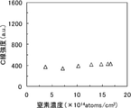
カソードルミネッセンス法により測定した発光スペクトルの例を図2及び図3に示した。図2は、酸素濃度が約0.2ppmaの場合で、図2(a)は窒素濃度が4.9×10¹⁴atoms/cm3、図2(b)は窒素濃度が約2.2×1015atoms/cm3の場合である。図2において、CiCsに由来するG線(1305nm付近)、CiOiに由来するC線(1570nm付近)が観測されているが、C線の発光強度が図2(a)と図2(b)とで明らかに異なっている。この結果から、窒素濃度が低い場合にCiOiの密度が低くなることがわかる。 Examples of emission spectra measured by the cathodoluminescence method are shown in FIGS. 2 and 3. FIG. 2 shows a case where the oxygen concentration is about 0.2 ppma, FIG. 2 (a) shows a nitrogen concentration of 4.9 × 10 14 atoms / cm 3 , and FIG. 2 (b) shows a nitrogen concentration of about 2.2 × 10. This is the case of 15 atoms / cm 3 . In FIG. 2, G line derived from CICS (near 1305 nm) and C line derived from CiOi (near 1570 nm) are observed, but the emission intensity of C line is shown in FIGS. 2 (a) and 2 (b). Is clearly different. From this result, it can be seen that the density of CiOi decreases when the nitrogen concentration is low.
図3は、酸素濃度が0.1ppma未満の場合で、図3(a)は窒素濃度が3.6×10¹⁴atoms/cm3、図3(b)は窒素濃度が約1.7×1015atoms/cm3の場合である。図3において、図2の場合と同様にG線とC線が観測されているが、G線の発光強度が図3(a)と図3(b)とで明らかに異なっている。この結果から、窒素濃度が低い場合にCiCsの密度が高くなることがわかる。図2及び図3において、シリコンに由来するTO線(1130nm付近)も観測されているが、発光強度が弱かったため、図のスケールではピークとして認識できない。 FIG. 3 shows the case where the oxygen concentration is less than 0.1 ppma, FIG. 3 (a) shows the nitrogen concentration of 3.6 × 10 14 atoms / cm 3 , and FIG. 3 (b) shows the nitrogen concentration of about 1.7 × 10. This is the case of 15 atoms / cm 3 . In FIG. 3, G-line and C-line are observed as in the case of FIG. 2, but the emission intensity of G-line is clearly different between FIGS. 3 (a) and 3 (b). From this result, it can be seen that the density of CICS increases when the nitrogen concentration is low. In FIGS. 2 and 3, TO rays derived from silicon (around 1130 nm) are also observed, but they cannot be recognized as peaks on the scale shown in the figure because the emission intensity is weak.
尚、本実験例において観測されたG線の発光波長(1305nm付近)は、一般的なG線の発光波長(1270nm付近)よりも長波長側にシフトしているが、同じ帰属であることが知られている。 The G-ray emission wavelength (around 1305 nm) observed in this experimental example is shifted to a longer wavelength side than the general G-line emission wavelength (around 1270 nm), but it is the same attribution. Are known.
次に、発光スペクトルからG線強度とC線強度を求めた。
酸素濃度が0.1ppma未満のシリコン単結晶基板の場合について、G線強度と窒素濃度との関係を図4に、C線強度と窒素濃度との関係を図5に示す。図4及び図5の結果から、酸素濃度が0.1ppma未満の場合には、C線強度は窒素濃度によらず低くなるが、G線強度は窒素濃度が高いほど低くなることがわかる。このことから、炭素濃度及び酸素濃度がほぼ同じでも、酸素濃度が0.1ppma未満の場合には、窒素濃度が高いほどCiCsの密度が低くなることがわかる。また、例えば、CiOiの密度を低く維持したまま、CiCsの密度を高くしたい場合には、酸素濃度を0.1ppma未満として、窒素濃度を低くすれば良いことがわかる。
Next, the G-line intensity and the C-line intensity were obtained from the emission spectrum.
In the case of a silicon single crystal substrate having an oxygen concentration of less than 0.1 ppma, the relationship between the G-ray intensity and the nitrogen concentration is shown in FIG. 4, and the relationship between the C-line intensity and the nitrogen concentration is shown in FIG. From the results of FIGS. 4 and 5, it can be seen that when the oxygen concentration is less than 0.1 ppma, the C-line intensity decreases regardless of the nitrogen concentration, but the G-line intensity decreases as the nitrogen concentration increases. From this, it can be seen that even if the carbon concentration and the oxygen concentration are almost the same, when the oxygen concentration is less than 0.1 ppma, the higher the nitrogen concentration, the lower the density of CICS. Further, for example, when it is desired to increase the density of CICS while maintaining the density of CICS low, it can be seen that the oxygen concentration should be less than 0.1 ppma and the nitrogen concentration should be lowered.
酸素濃度が0.1~0.3ppmaのシリコン単結晶基板の場合について、G線強度と窒素濃度との関係を図6に、C線強度と窒素濃度との関係を図7に示す。図6及び図7の結果から、酸素濃度が0.1~0.3ppmaの場合には、G線強度は窒素濃度によらず低くなるが、C線強度は窒素濃度が高いほど高くなることがわかる。このことから、炭素濃度及び酸素濃度がほぼ同じでも、酸素濃度が0.1~0.3ppmaの場合には、窒素濃度が高いほどCiOiの密度が高くなることがわかる。また、例えば、CiCsの密度を低く維持したまま、CiOiの密度を高くしたい場合には、酸素濃度を0.1~0.3ppmaとして、窒素濃度を高くすれば良いことがわかる。 In the case of a silicon single crystal substrate having an oxygen concentration of 0.1 to 0.3 ppma, the relationship between the G-ray intensity and the nitrogen concentration is shown in FIG. 6, and the relationship between the C-line intensity and the nitrogen concentration is shown in FIG. From the results of FIGS. 6 and 7, when the oxygen concentration is 0.1 to 0.3 ppma, the G-ray intensity decreases regardless of the nitrogen concentration, but the C-line intensity increases as the nitrogen concentration increases. Recognize. From this, it can be seen that even if the carbon concentration and the oxygen concentration are almost the same, when the oxygen concentration is 0.1 to 0.3 ppma, the higher the nitrogen concentration, the higher the density of CiOi. Further, for example, when it is desired to increase the density of CiOi while maintaining the density of CiCs low, it can be seen that the oxygen concentration should be set to 0.1 to 0.3 ppma and the nitrogen concentration should be increased.
フォトルミネッセンス法でもカソードルミネッセンス法と同じ発光線が観測されることがわかっているので、フォトルミネッセンス法でも同様な方法により、G線強度及びC線強度と窒素濃度との関係を求めることができる。 Since it is known that the same emission line as the cathode luminescence method is observed in the photoluminescence method, the relationship between the G-ray intensity and the C-line intensity and the nitrogen concentration can be obtained by the same method in the photoluminescence method.
FZシリコン単結晶基板の酸素濃度は、結晶製造時に用いるシリコン原料が多結晶シリコンかCZ法で育成した単結晶シリコンかによって異なるが、シリコン原料の製法が同じであれば、酸素濃度のばらつきを小さくすることができる。 The oxygen concentration of the FZ silicon single crystal substrate differs depending on whether the silicon raw material used in crystal production is polycrystalline silicon or single crystal silicon grown by the CZ method, but if the manufacturing method of the silicon raw material is the same, the variation in oxygen concentration is small. can do.
このことから、いずれの原料を用いたFZシリコン単結晶基板の場合でも、窒素濃度を調整することで炭素、あるいは炭素及び酸素を含む複合体の密度を制御できることがわかる。 From this, it can be seen that the density of carbon or a complex containing carbon and oxygen can be controlled by adjusting the nitrogen concentration in the case of the FZ silicon single crystal substrate using any of the raw materials.
以上のように、電子線照射とその後の熱処理を施した場合の欠陥密度が目標値になるように、欠陥密度を制御するシリコン単結晶基板の窒素濃度を調整することにより欠陥密度を制御すれば、シリコン単結晶基板自体に起因する欠陥密度のばらつきを小さくすることができる。そして、窒素濃度のばらつきを小さくすることにより、欠陥密度のばらつきを小さくすることができる。 As described above, if the defect density is controlled by adjusting the nitrogen concentration of the silicon single crystal substrate that controls the defect density so that the defect density after electron beam irradiation and the subsequent heat treatment becomes the target value. , The variation in defect density caused by the silicon single crystal substrate itself can be reduced. Then, by reducing the variation in the nitrogen concentration, the variation in the defect density can be reduced.
上記のように、電子線照射とその後の熱処理を施した場合の欠陥密度が窒素濃度に依存する理由は、以下のように考えられる。 As described above, the reason why the defect density in the case of electron beam irradiation and subsequent heat treatment depends on the nitrogen concentration is considered as follows.
シリコン基板に対して、高エネルギーの粒子線を照射すると、格子位置のシリコン原子が弾き出されて、格子間シリコン(I)とその抜け殻である空孔(V)が生成される。過剰に生成されたIやVは、単体では不安定なため、再結合したり(V+I→0)、I同士やV同士がクラスタリングしたり、シリコン基板中に含まれる軽元素不純物と反応して複合体を形成する。そして、IやVのクラスターや、IやVと軽元素不純物の複合体は、シリコンのバンドギャップ中に深い準位を形成して、キャリアの再結合中心や捕獲中心として働き、デバイス特性に影響する。 When a silicon substrate is irradiated with a high-energy particle beam, silicon atoms at lattice positions are ejected to generate interstitial silicon (I) and pores (V) which are shells thereof. Since I and V generated excessively are unstable by themselves, they may recombine (V + I → 0), cluster I or V with each other, or react with light element impurities contained in the silicon substrate. Form a complex. The clusters of I and V and the complex of I and V and light element impurities form deep levels in the bandgap of silicon and act as carrier recombination centers and capture centers, affecting device characteristics. do.
空孔Vに関連する欠陥として、Vと置換型リンPsが反応してVPが形成される(V+Ps→VP)ことが知られている。また、Vと格子間酸素Oiが反応してVOが形成され(V+Oi→VO)、更に、VとVOが反応してV2O(V+VO→V2O)が形成される場合もある。また、V同士が反応してVVも形成される(V+V→VV)。窒素が存在する場合には、VとNが反応してVNも形成されることになる(V+N→VN)。VとP、O、あるいはNとの反応はそれぞれ競合するため、窒素濃度が高い場合にVNが形成されやすくなるとすると、Vが関連した他の複合体が形成されにくくなる可能性がある。 As a defect related to the pore V, it is known that V reacts with substituted phosphorus Ps to form VP (V + Ps → VP). Further, V and interstitial oxygen Oi may react to form VO (V + Oi → VO), and V and VO may react to form V 2 O (V + VO → V 2 O). Further, Vs react with each other to form VV (V + V → VV). In the presence of nitrogen, V and N react to form VN (V + N → VN). Since the reactions of V and P, O, or N compete with each other, if VN is likely to be formed when the nitrogen concentration is high, it may be difficult to form other V-related complexes.
一方、格子間シリコンIが関連する欠陥として、Iと置換型ボロンBsが反応して格子間ボロンBiが形成され(I+Bs→Bi)、更に、BiとOiが反応してBiOiが形成される(Bi+Oi→BiOi)ことが知られている。また、炭素が存在する場合、Iと置換型炭素Csが反応して格子間炭素Ciが形成され(I+Cs→Ci)、更に、CiとOi、CiとCsが反応してCiOi、CiCsが形成される(Ci+Oi→CiOi、Ci+Cs→CiCs)。また、I同士が反応してIクラスターも形成される(I+I+…→In)。窒素がより高濃度で存在する場合には、VとNが反応することにより、VとIの再結合が抑制され、その結果として、Iが関連した複合体が形成されやすくなる可能性がある。 On the other hand, as a defect related to the interstitial silicon I, I reacts with the substituted boron Bs to form interstitial boron Bi (I + Bs → Bi), and Bi reacts with Oi to form BiOi (I + Bs → Bi). Bi + Oi → BiOi) is known. In the presence of carbon, I reacts with substituted carbon Cs to form interstitial carbon Ci (I + Cs → Ci), and Ci reacts with Oi and Ci with Cs to form CiOi and CiCs. (Ci + Oi → CiOi, Ci + Cs → CiCs). In addition, I react with each other to form an I cluster (I + I + ... → In). In the presence of higher concentrations of nitrogen, the reaction of V and N may suppress the recombination of V and I, resulting in the formation of I-related complexes. ..
IやVと軽元素不純物との反応は、それぞれの絶対濃度と濃度バランスに依存するため、極めて複雑であり、更に熱処理が施された場合には、複合体の消滅や形態変化が起こるため、更に複雑になる。 The reaction between I and V and light element impurities is extremely complicated because it depends on the absolute concentration and concentration balance of each, and when heat treatment is applied, the complex disappears and the morphology changes. It gets even more complicated.
上述の実験例の結果において、酸素濃度が0.1~0.3ppmaの場合に窒素濃度が高いほどCiOi密度が高くなるのは、VとNが反応することにより、VとIの再結合が抑制され、その結果として、Iが関連した複合体が形成されやすくなるためと考えられる。また、酸素濃度が0.1ppma未満の場合に窒素濃度によらずCiOi密度が低くなるのは、Oi濃度が低いことにより、窒素濃度によらずCiOiの形成が抑制されるためと考えられる。一方、CiCsに関しては、CiOiと同様にIが関連した複合体であるが、CiOiと異なる挙動になる理由は今のところ明らかではない。 In the results of the above experimental example, when the oxygen concentration is 0.1 to 0.3 ppma, the higher the nitrogen concentration, the higher the CiOi density, because the reaction between V and N causes the recombination of V and I. It is believed that this is because it is suppressed, and as a result, I-related complexes are more likely to be formed. Further, it is considered that the reason why the CiOi density is low regardless of the nitrogen concentration when the oxygen concentration is less than 0.1 ppma is that the formation of CiOi is suppressed regardless of the nitrogen concentration due to the low Oi concentration. On the other hand, regarding CICS, although it is a complex in which I is related like CiOi, the reason why it behaves differently from CiOi is not clear at present.
以下、実施例及び比較例を用いて本発明をより具体的に説明するが、本発明はこれらに限定されるものではない。 Hereinafter, the present invention will be described in more detail with reference to Examples and Comparative Examples, but the present invention is not limited thereto.
[実施例1]
図1に示すような、本発明の欠陥密度の制御方法でシリコン単結晶基板中の欠陥密度の制御を行った。このとき、実験例と同様にカソードルミネッセンス法で測定した場合に、C線強度が2000程度になるように制御することを目標とした。
[Example 1]
The defect density in the silicon single crystal substrate was controlled by the defect density control method of the present invention as shown in FIG. At this time, the goal was to control the C-line intensity to about 2000 when measured by the cathode luminescence method as in the experimental example.
まず、測定工程において、窒素濃度が異なる複数の試験用シリコン単結晶基板に、電子線を照射した後、熱処理を行い、複数の試験用シリコン単結晶基板におけるC線強度を測定した。試験用シリコン単結晶基板はFZ法により育成されたシリコン単結晶から製造されたものであり、酸素濃度は0.1~0.3ppmaとした。
このときの電子線の照射線量は1×10¹⁵/cm2とし、電子線の加速電圧は2MVとした。またこのとき、熱処理の温度は360℃、時間は45分、雰囲気は窒素とした。
First, in the measurement step, a plurality of test silicon single crystal substrates having different nitrogen concentrations were irradiated with an electron beam and then heat-treated to measure the C-ray intensity in the plurality of test silicon single crystal substrates. The test silicon single crystal substrate was produced from a silicon single crystal grown by the FZ method, and the oxygen concentration was 0.1 to 0.3 ppma.
The irradiation dose of the electron beam at this time was 1 × 10 15 / cm 2 , and the acceleration voltage of the electron beam was 2 MV. At this time, the temperature of the heat treatment was 360 ° C., the time was 45 minutes, and the atmosphere was nitrogen.
次に、相関関係取得工程において、C線強度と複数の試験用シリコン単結晶基板の窒素濃度との相関関係を取得した(図7)。
次に、上記相関関係に基づいて、熱処理工程後のシリコン単結晶基板のC線強度が目標値(2000程度)になるように、準備工程で準備するシリコン単結晶基板の窒素濃度を調整した。このとき、準備したシリコン単結晶基板は、CZ法により育成されたシリコン単結晶インゴットを原料として、FZ法により育成されたシリコン単結晶から製造されたものであり、酸素濃度は約0.2ppmaで、窒素濃度を1.7×10¹⁵atoms/cm3に調整したものであった。
Next, in the correlation acquisition step, the correlation between the C-ray intensity and the nitrogen concentration of the plurality of test silicon single crystal substrates was acquired (FIG. 7).
Next, based on the above correlation, the nitrogen concentration of the silicon single crystal substrate prepared in the preparation step was adjusted so that the C-line intensity of the silicon single crystal substrate after the heat treatment step became a target value (about 2000). At this time, the prepared silicon single crystal substrate is manufactured from a silicon single crystal grown by the FZ method using a silicon single crystal ingot grown by the CZ method as a raw material, and has an oxygen concentration of about 0.2 ppma. , The nitrogen concentration was adjusted to 1.7 × 10 15 singles / cm 3 .
その後、準備したシリコン単結晶基板に電子線を照射した。電子線の照射線量は1×10¹⁵/cm2とし、電子線の加速電圧は2MVとした。次に、電子線照射したシリコン単結晶基板に回復熱処理を施した。回復熱処理の温度は360℃とし、雰囲気は窒素、時間は45分とした。 Then, the prepared silicon single crystal substrate was irradiated with an electron beam. The irradiation dose of the electron beam was 1 × 10 15 / cm 2 , and the acceleration voltage of the electron beam was 2 MV. Next, the silicon single crystal substrate irradiated with the electron beam was subjected to a recovery heat treatment. The temperature of the recovery heat treatment was 360 ° C., the atmosphere was nitrogen, and the time was 45 minutes.
回復熱処理後のC線強度をカソードルミネッセンス法により測定した結果、シリコン単結晶基板のC線強度は2008であった。 As a result of measuring the C-line intensity after the recovery heat treatment by the cathode luminescence method, the C-line intensity of the silicon single crystal substrate was 2008.
このように、実施例1では、シリコン単結晶基板の窒素濃度を調整することにより、目標値の欠陥密度を得ることができることが確認できた。 As described above, in Example 1, it was confirmed that the defect density of the target value can be obtained by adjusting the nitrogen concentration of the silicon single crystal substrate.
また、上記で取得した相関関係に基づき、窒素濃度を1.5×10¹⁵~1.9×10¹⁵atoms/cm3の範囲に調整したFZシリコン単結晶基板を5枚準備し、上記と同様の条件で、電子線照射と回復熱処理を行った後、C線強度をカソードルミネッセンス法により測定した。その結果、C線強度は1830、2105、1955、2161、1876となり、シリコン単結晶基板自体に起因する欠陥密度のばらつきを非常に小さく抑えられることが確認できた。 Further, based on the correlation obtained above, five FZ silicon single crystal substrates having a nitrogen concentration adjusted to the range of 1.5 × 10 15 to 1.9 × 10 15 atoms / cm 3 were prepared, and the same as above. After performing electron beam irradiation and recovery heat treatment under the above conditions, the C-ray intensity was measured by the cathode luminescence method. As a result, the C-line intensities were 1830, 2105, 1955, 2161, and 1876, and it was confirmed that the variation in defect density due to the silicon single crystal substrate itself could be suppressed to a very small level.
[比較例1]
試験用シリコン単結晶基板を使用して、欠陥密度と窒素濃度との相関関係を取得せず、準備するシリコン単結晶基板の窒素濃度を上記相関関係に基づいて調整しなかったこと以外、実施例1と同様の条件でシリコン単結晶基板の欠陥密度を制御した。
このとき、窒素濃度が1.0×10¹⁵atoms/cm3、酸素濃度が0.1ppma未満のFZシリコン単結晶基板に、電子線を照射した後、回復熱処理を施した。
[Comparative Example 1]
Examples except that the correlation between the defect density and the nitrogen concentration was not obtained by using the test silicon single crystal substrate, and the nitrogen concentration of the prepared silicon single crystal substrate was not adjusted based on the above correlation. The defect density of the silicon single crystal substrate was controlled under the same conditions as in 1.
At this time, an FZ silicon single crystal substrate having a nitrogen concentration of 1.0 × 10 15 atoms / cm 3 and an oxygen concentration of less than 0.1 ppma was irradiated with an electron beam and then subjected to a recovery heat treatment.
続いて、実施例1と同様の条件で回復熱処理後のC線強度をカソードルミネッセンス法により測定した結果、395であった。 Subsequently, the C-ray intensity after the recovery heat treatment was measured by the cathode luminescence method under the same conditions as in Example 1, and the result was 395.
このように、比較例1では、電子線照射条件と回復熱処理条件を実施例1と同様の条件にしたにも関わらず、シリコン単結晶基板のC線強度は目標値の2000から大きく離れた値になってしまうことが確認された。 As described above, in Comparative Example 1, the C-ray intensity of the silicon single crystal substrate was significantly different from the target value of 2000, even though the electron beam irradiation conditions and the recovery heat treatment conditions were the same as those of Example 1. It was confirmed that it would become.
また、窒素濃度及び酸素濃度の異なるFZシリコン単結晶基板を無作為に5枚準備し、上記と同様の条件で、電子線照射と回復熱処理を行った後、C線強度をカソードルミネッセンス法により測定した結果、C線強度は1157、2276、377、435、1717となり、実施例1と比べてシリコン単結晶基板自体に起因する欠陥密度のばらつきが著しく大きくなることが確認された。 In addition, five FZ silicon single crystal substrates having different nitrogen and oxygen concentrations were randomly prepared, and after performing electron beam irradiation and recovery heat treatment under the same conditions as above, the C-ray intensity was measured by the cathode luminescence method. As a result, the C-ray intensities were 1157, 2276, 377, 435, and 1717, and it was confirmed that the variation in the defect density due to the silicon single crystal substrate itself was significantly larger than that in Example 1.
[実施例2]
図1に示すような、本発明の欠陥密度の制御方法でシリコン単結晶基板中の欠陥密度の制御を行った。このとき、実験例と同様にカソードルミネッセンス法で測定した場合に、G線強度が1200程度になるように制御することを目標とした。
[Example 2]
The defect density in the silicon single crystal substrate was controlled by the defect density control method of the present invention as shown in FIG. At this time, the goal was to control the G-ray intensity to be about 1200 when measured by the cathode luminescence method as in the experimental example.
まず、測定工程において、窒素濃度が異なる複数の試験用シリコン単結晶基板に、電子線を照射した後、熱処理を行い、複数の試験用シリコン単結晶基板におけるG線強度を測定した。試験用シリコン単結晶基板は、多結晶シリコンインゴットを原料として、FZ法により育成されたシリコン単結晶から製造されたものであり、酸素濃度は0.1ppma未満であった。
このときの電子線の照射線量は1×10¹⁵/cm2とし、電子線の加速電圧は2MeVとした。またこのとき、熱処理の温度は360℃、時間は45分、雰囲気は窒素とした。
First, in the measurement step, a plurality of test silicon single crystal substrates having different nitrogen concentrations were irradiated with an electron beam and then heat-treated to measure the G-ray intensity in the plurality of test silicon single crystal substrates. The test silicon single crystal substrate was produced from a silicon single crystal grown by the FZ method using a polysilicon silicon ingot as a raw material, and the oxygen concentration was less than 0.1 ppma.
The irradiation dose of the electron beam at this time was 1 × 10 15 / cm 2 , and the acceleration voltage of the electron beam was 2 MeV. At this time, the temperature of the heat treatment was 360 ° C., the time was 45 minutes, and the atmosphere was nitrogen.
次に、相関関係取得工程において、G線強度と複数の試験用シリコン単結晶基板の窒素濃度との相関関係を取得した(図4)。
次に、上記相関関係に基づいて、熱処理工程後のシリコン単結晶基板のG線強度が目標値(1200程度)になるように、準備工程で準備するシリコン単結晶基板の窒素濃度を調整した。このとき、準備したシリコン単結晶基板は、多結晶シリコンインゴットを原料として、FZ法により育成されたシリコン単結晶から製造されたものであり、酸素濃度は0.1ppma未満で、窒素濃度を1.0×10¹⁵atoms/cm3に調整したものであった。
Next, in the correlation acquisition step, the correlation between the G-ray intensity and the nitrogen concentration of the plurality of test silicon single crystal substrates was acquired (FIG. 4).
Next, based on the above correlation, the nitrogen concentration of the silicon single crystal substrate prepared in the preparation step was adjusted so that the G-ray intensity of the silicon single crystal substrate after the heat treatment step became a target value (about 1200). At this time, the prepared silicon single crystal substrate was manufactured from a silicon single crystal grown by the FZ method using a polysilicon silicon ingot as a raw material, and the oxygen concentration was less than 0.1 ppma and the nitrogen concentration was 1. It was adjusted to 0 × 10 15 atoms / cm 3 .
その後、準備したシリコン単結晶基板に電子線を照射した。電子線の照射線量は1×10¹⁵/cm2とし、電子線の加速電圧は2MVとした。次に、電子線照射したシリコン単結晶基板に回復熱処理を施した。回復熱処理の温度は360℃とし、雰囲気は窒素、時間は45分とした。 Then, the prepared silicon single crystal substrate was irradiated with an electron beam. The irradiation dose of the electron beam was 1 × 10 15 / cm 2 , and the acceleration voltage of the electron beam was 2 MV. Next, the silicon single crystal substrate irradiated with the electron beam was subjected to a recovery heat treatment. The temperature of the recovery heat treatment was 360 ° C., the atmosphere was nitrogen, and the time was 45 minutes.
回復熱処理後のG線強度をカソードルミネッセンス法により測定した結果、シリコン単結晶基板のG線強度は1225であった。 As a result of measuring the G-ray intensity after the recovery heat treatment by the cathode luminescence method, the G -ray intensity of the silicon single crystal substrate was 1225.
このように、実施例2では、シリコン単結晶基板の窒素濃度を調整することにより、欠陥密度の目標値を得ることができることが確認できた。 As described above, in Example 2 , it was confirmed that the target value of the defect density can be obtained by adjusting the nitrogen concentration of the silicon single crystal substrate.
また、上記で取得した相関関係に基づき、窒素濃度を0.9×10¹⁵~1.1×10¹⁵atoms/cm3の範囲に調整したFZシリコン単結晶基板を5枚準備し、上記と同様の条件で、電子線照射と回復熱処理を行った後、G線強度をカソードルミネッセンス法により測定した。その結果、G線強度は1170、1221、1195、1177、1265となり、シリコン単結晶基板自体に起因する欠陥密度のばらつきを非常に小さく抑えられることが確認できた。 Further, based on the correlation obtained above, five FZ silicon single crystal substrates having a nitrogen concentration adjusted to the range of 0.9 × 10 15 to 1.1 × 10 15 atoms / cm 3 were prepared, and the same as above. After performing electron beam irradiation and recovery heat treatment under the above conditions, the G-ray intensity was measured by the cathode luminescence method. As a result, the G-ray intensities were 1170, 1221, 1195, 1177, and 1265, and it was confirmed that the variation in the defect density due to the silicon single crystal substrate itself could be suppressed to a very small level.
[比較例2]
試験用シリコン単結晶基板を使用して、欠陥密度と窒素濃度との相関関係を取得せず、準備するシリコン単結晶基板の窒素濃度を上記相関関係に基づいて調整しなかったこと以外、実施例2と同様の条件でシリコン単結晶基板の欠陥密度を制御した。
このとき、窒素濃度は1.7×10¹⁵atoms/cm3、酸素濃度は0.1ppma未満であった。このFZシリコン単結晶基板に、電子線を照射した後、回復熱処理を施した。
[Comparative Example 2]
Examples except that the correlation between the defect density and the nitrogen concentration was not obtained by using the test silicon single crystal substrate, and the nitrogen concentration of the prepared silicon single crystal substrate was not adjusted based on the above correlation. The defect density of the silicon single crystal substrate was controlled under the same conditions as in 2 .
At this time, the nitrogen concentration was 1.7 × 10 15 atoms / cm 3 , and the oxygen concentration was less than 0.1 ppma. The FZ silicon single crystal substrate was irradiated with an electron beam and then subjected to a recovery heat treatment.
続いて、実施例2と同様の条件で回復熱処理後のG線強度をカソードルミネッセンス法により測定した結果、792であった。 Subsequently, the G-ray intensity after the recovery heat treatment was measured by the cathode luminescence method under the same conditions as in Example 2, and the result was 792.
このように、比較例2では、電子線照射条件と回復熱処理条件を実施例2と同様の条件にしたにも関わらず、シリコン単結晶基板のG線強度は目標値の1200から大きく離れた値になってしまうことが確認された。 As described above, in Comparative Example 2, the G-ray intensity of the silicon single crystal substrate was significantly different from the target value of 1200, even though the electron beam irradiation conditions and the recovery heat treatment conditions were the same as those of Example 2. It was confirmed that it would become.
また、窒素濃度及び酸素濃度の異なるFZシリコン単結晶基板を無作為に5枚準備し、上記と同様の条件で、電子線照射と回復熱処理を行った後、G線強度をカソードルミネッセンス法により測定した結果、G線強度は280、286、1480、841、275となり、実施例1と比べてシリコン単結晶基板自体に起因する欠陥密度のばらつきが著しく大きくなることが確認された。 In addition, five FZ silicon single crystal substrates having different nitrogen and oxygen concentrations were randomly prepared, and after performing electron beam irradiation and recovery heat treatment under the same conditions as above, the G-ray intensity was measured by the cathode luminescence method. As a result, the G-ray intensities were 280, 286, 1480, 841, 275, and it was confirmed that the variation in the defect density due to the silicon single crystal substrate itself was significantly larger than that in Example 1.
なお、本発明は、上記実施形態に限定されるものではない。上記実施形態は例示であり、本発明の特許請求の範囲に記載された技術的思想と実質的に同一な構成を有し、同様な作用効果を奏するものは、いかなるものであっても本発明の技術的範囲に包含される。 The present invention is not limited to the above embodiment. The above-described embodiment is an example, and the present invention can be anything that has substantially the same configuration as the technical idea described in the claims of the present invention and exhibits the same function and effect. Is included in the technical scope of.
Claims (4)
前記準備したシリコン単結晶基板に電子線を、1×10 13 ~1×10 15 /cm 2 の線量で、0.5~2MVの加速電圧で照射する電子線照射工程と、
該電子線照射工程後の前記シリコン単結晶基板に熱処理を施す熱処理工程と
を行うシリコン単結晶基板中の欠陥密度の制御方法であって、
前記準備工程を行う前に予め、窒素濃度が異なる複数の試験用シリコン単結晶基板に前記電子線を前記線量及び前記加速電圧で照射した後、熱処理を行い、前記複数の試験用シリコン単結晶基板中に発生した欠陥密度を測定する測定工程と、
前記測定した欠陥密度と前記窒素濃度との相関関係を取得する相関関係取得工程とを有し、
前記取得した相関関係に基づいて、前記熱処理工程後の前記シリコン単結晶基板中の欠陥密度が目標値になるように、前記準備工程で準備する前記シリコン単結晶基板の窒素濃度を調整し、
前記欠陥密度を制御する対象とする欠陥を、炭素、あるいは炭素及び酸素を含む複合体とすることを特徴とするシリコン単結晶基板中の欠陥密度の制御方法。 The preparatory process for preparing a silicon single crystal substrate that controls the defect density,
An electron beam irradiation step of irradiating the prepared silicon single crystal substrate with an electron beam at a dose of 1 × 10 13 to 1 × 10 15 / cm 2 at an acceleration voltage of 0.5 to 2 MV .
A method for controlling the defect density in a silicon single crystal substrate, which is a heat treatment step of heat-treating the silicon single crystal substrate after the electron beam irradiation step.
Before performing the preparatory step, a plurality of test silicon single crystal substrates having different nitrogen concentrations are irradiated with the electron beam at the dose and the acceleration voltage, and then heat-treated to perform the plurality of test silicon single crystal substrates. A measurement process that measures the defect density generated inside, and
It has a correlation acquisition step of acquiring the correlation between the measured defect density and the nitrogen concentration.
Based on the obtained correlation, the nitrogen concentration of the silicon single crystal substrate prepared in the preparation step is adjusted so that the defect density in the silicon single crystal substrate after the heat treatment step becomes a target value .
A method for controlling the defect density in a silicon single crystal substrate, wherein the defect whose target is to control the defect density is carbon or a complex containing carbon and oxygen .
The method according to any one of claims 1 to 3 , wherein in the preparation step, a silicon single crystal substrate whose variation in nitrogen concentration is adjusted to within 10% with respect to the target nitrogen concentration value is prepared. The method for controlling the defect density in the silicon single crystal substrate described.
Priority Applications (6)
| Application Number | Priority Date | Filing Date | Title |
|---|---|---|---|
| JP2018112062A JP7006517B2 (en) | 2018-06-12 | 2018-06-12 | How to control the defect density in a silicon single crystal substrate |
| CN201980039589.7A CN112334608B (en) | 2018-06-12 | 2019-05-13 | Method for controlling defect density in single crystal silicon substrate |
| PCT/JP2019/019004 WO2019239762A1 (en) | 2018-06-12 | 2019-05-13 | Method for controlling defect density in silicon single crystal substrate |
| EP19820517.1A EP3808879B1 (en) | 2018-06-12 | 2019-05-13 | Method for controlling defect density in silicon single crystal substrate |
| DK19820517.1T DK3808879T3 (en) | 2018-06-12 | 2019-05-13 | METHOD FOR CONTROLLING DEFECT DENSITY IN A MONOCRYSTALLINE SILICON SUBSTRATE |
| TW108117522A TWI801586B (en) | 2018-06-12 | 2019-05-21 | Method for controlling defect density in single crystal silicon substrate |
Applications Claiming Priority (1)
| Application Number | Priority Date | Filing Date | Title |
|---|---|---|---|
| JP2018112062A JP7006517B2 (en) | 2018-06-12 | 2018-06-12 | How to control the defect density in a silicon single crystal substrate |
Publications (3)
| Publication Number | Publication Date |
|---|---|
| JP2019214488A JP2019214488A (en) | 2019-12-19 |
| JP2019214488A5 JP2019214488A5 (en) | 2020-12-10 |
| JP7006517B2 true JP7006517B2 (en) | 2022-01-24 |
Family
ID=68842170
Family Applications (1)
| Application Number | Title | Priority Date | Filing Date |
|---|---|---|---|
| JP2018112062A Active JP7006517B2 (en) | 2018-06-12 | 2018-06-12 | How to control the defect density in a silicon single crystal substrate |
Country Status (6)
| Country | Link |
|---|---|
| EP (1) | EP3808879B1 (en) |
| JP (1) | JP7006517B2 (en) |
| CN (1) | CN112334608B (en) |
| DK (1) | DK3808879T3 (en) |
| TW (1) | TWI801586B (en) |
| WO (1) | WO2019239762A1 (en) |
Families Citing this family (2)
| Publication number | Priority date | Publication date | Assignee | Title |
|---|---|---|---|---|
| EP4123686A4 (en) * | 2020-03-17 | 2024-05-01 | Shin-Etsu Handotai Co., Ltd. | Method for controlling donor concentration in silicon single crystal substrate |
| JP7264100B2 (en) * | 2020-04-02 | 2023-04-25 | 信越半導体株式会社 | Method for controlling donor concentration in silicon single crystal substrate |
Citations (5)
| Publication number | Priority date | Publication date | Assignee | Title |
|---|---|---|---|---|
| JP2001068477A (en) | 1999-08-27 | 2001-03-16 | Komatsu Electronic Metals Co Ltd | Epitaxial silicon wafer |
| JP2001240490A (en) | 2000-02-25 | 2001-09-04 | Sumitomo Metal Ind Ltd | Semiconductor silicon wafer manufacturing method |
| JP2004304095A (en) | 2003-04-01 | 2004-10-28 | Sumitomo Mitsubishi Silicon Corp | Silicon wafer, and manufacturing method thereof |
| JP2015023062A (en) | 2013-07-16 | 2015-02-02 | 信越半導体株式会社 | Method of manufacturing diffused wafer |
| JP2015156420A (en) | 2014-02-20 | 2015-08-27 | 信越半導体株式会社 | Evaluation method for carbon concentration in silicon single crystal, and method of manufacturing semiconductor device |
Family Cites Families (9)
| Publication number | Priority date | Publication date | Assignee | Title |
|---|---|---|---|---|
| JP3211874B2 (en) | 1997-10-29 | 2001-09-25 | サンケン電気株式会社 | Method for manufacturing semiconductor device |
| JP4288797B2 (en) | 1998-11-05 | 2009-07-01 | 株式会社デンソー | Manufacturing method of semiconductor device |
| JP2001067477A (en) * | 1999-08-27 | 2001-03-16 | Matsushita Electric Ind Co Ltd | Individual identification system |
| JP2006054350A (en) * | 2004-08-12 | 2006-02-23 | Komatsu Electronic Metals Co Ltd | Nitrogen-doped silicon wafer and its manufacturing method |
| WO2007055352A1 (en) | 2005-11-14 | 2007-05-18 | Fuji Electric Device Technology Co., Ltd. | Semiconductor device and method for manufacturing same |
| EP2800143B1 (en) | 2011-12-28 | 2020-04-08 | Fuji Electric Co., Ltd. | Semiconductor device and method for producing semiconductor device |
| JP6036670B2 (en) * | 2013-12-10 | 2016-11-30 | 信越半導体株式会社 | Defect concentration evaluation method for silicon single crystal substrate |
| JP6083412B2 (en) * | 2014-04-01 | 2017-02-22 | 信越半導体株式会社 | Method for controlling recombination lifetime and method for manufacturing silicon substrate |
| JP6447351B2 (en) * | 2015-05-08 | 2019-01-09 | 株式会社Sumco | Method for manufacturing silicon epitaxial wafer and silicon epitaxial wafer |
-
2018
- 2018-06-12 JP JP2018112062A patent/JP7006517B2/en active Active
-
2019
- 2019-05-13 WO PCT/JP2019/019004 patent/WO2019239762A1/en unknown
- 2019-05-13 DK DK19820517.1T patent/DK3808879T3/en active
- 2019-05-13 EP EP19820517.1A patent/EP3808879B1/en active Active
- 2019-05-13 CN CN201980039589.7A patent/CN112334608B/en active Active
- 2019-05-21 TW TW108117522A patent/TWI801586B/en active
Patent Citations (5)
| Publication number | Priority date | Publication date | Assignee | Title |
|---|---|---|---|---|
| JP2001068477A (en) | 1999-08-27 | 2001-03-16 | Komatsu Electronic Metals Co Ltd | Epitaxial silicon wafer |
| JP2001240490A (en) | 2000-02-25 | 2001-09-04 | Sumitomo Metal Ind Ltd | Semiconductor silicon wafer manufacturing method |
| JP2004304095A (en) | 2003-04-01 | 2004-10-28 | Sumitomo Mitsubishi Silicon Corp | Silicon wafer, and manufacturing method thereof |
| JP2015023062A (en) | 2013-07-16 | 2015-02-02 | 信越半導体株式会社 | Method of manufacturing diffused wafer |
| JP2015156420A (en) | 2014-02-20 | 2015-08-27 | 信越半導体株式会社 | Evaluation method for carbon concentration in silicon single crystal, and method of manufacturing semiconductor device |
Non-Patent Citations (1)
| Title |
|---|
| SGOUROU, E. N. et al.,Infrared study of defects in nitrogen-doped electron irradiated silicon,J. Mater. Sci.: Mater. Electron.,スイス,Springer Nature Switzerland AG,2015年11月04日,Vol. 27, No. 2,pp. 2054-2061,DOI: 10.1007/s10854-015-3991-2 |
Also Published As
| Publication number | Publication date |
|---|---|
| TWI801586B (en) | 2023-05-11 |
| WO2019239762A1 (en) | 2019-12-19 |
| EP3808879A4 (en) | 2022-03-02 |
| CN112334608A (en) | 2021-02-05 |
| DK3808879T3 (en) | 2023-05-01 |
| JP2019214488A (en) | 2019-12-19 |
| EP3808879A1 (en) | 2021-04-21 |
| CN112334608B (en) | 2022-07-26 |
| EP3808879B1 (en) | 2023-03-01 |
| TW202002116A (en) | 2020-01-01 |
Similar Documents
| Publication | Publication Date | Title |
|---|---|---|
| JP6268039B2 (en) | Calibration curve creation method, impurity concentration measurement method, and semiconductor wafer manufacturing method | |
| JP6075307B2 (en) | Method for evaluating carbon concentration in silicon single crystal and method for manufacturing semiconductor device | |
| KR101536512B1 (en) | Saturation voltage estimation method and silicon epitaxial wafer manufacturing method | |
| JP6083412B2 (en) | Method for controlling recombination lifetime and method for manufacturing silicon substrate | |
| JP6048381B2 (en) | Method for evaluating carbon concentration in silicon single crystal and method for manufacturing semiconductor device | |
| JP6292131B2 (en) | Silicon substrate sorting method | |
| KR102029647B1 (en) | Defect density evaluation method for silicon single-crystal substrate | |
| JP7006517B2 (en) | How to control the defect density in a silicon single crystal substrate | |
| Nakamura et al. | Size and dopant-concentration dependence of photoluminescence properties of ion-implanted phosphorus-and boron-codoped Si nanocrystals | |
| JP6881292B2 (en) | How to control rejoin lifetime | |
| CN111033709B (en) | Composite life control method | |
| JP6922688B2 (en) | Selection method of silicon single crystal substrate and silicon single crystal substrate | |
| Inoue et al. | Infrared defect dynamics–radiation induced complexes in silicon crystals grown by various techniques | |
| JP6766786B2 (en) | Carbon concentration evaluation method in silicon single crystal substrate and manufacturing method of semiconductor device | |
| JP7103314B2 (en) | Carbon concentration evaluation method in silicon single crystal substrate | |
| JP7259791B2 (en) | Method for evaluating effect of reducing white spot defects by implanting cluster ions into silicon wafer and method for manufacturing epitaxial silicon wafer | |
| JP7334849B2 (en) | Method for controlling donor concentration in silicon single crystal substrate | |
| Kozlovski et al. | Conductivity compensation in CVD-grown n-4H-SiC under irradiation with 0.9 MeV electrons | |
| JP2021163929A (en) | Control method for donor concentration in silicon single-crystal substrate | |
| CN111801782A (en) | Carbon concentration evaluation method | |
| Snyman et al. | Photoluminescence of proton‐bombarded and annealed GaAs |
Legal Events
| Date | Code | Title | Description |
|---|---|---|---|
| A521 | Request for written amendment filed |
Free format text: JAPANESE INTERMEDIATE CODE: A523 Effective date: 20180614 |
|
| A521 | Request for written amendment filed |
Free format text: JAPANESE INTERMEDIATE CODE: A523 Effective date: 20190513 |
|
| A621 | Written request for application examination |
Free format text: JAPANESE INTERMEDIATE CODE: A621 Effective date: 20200518 |
|
| A521 | Request for written amendment filed |
Free format text: JAPANESE INTERMEDIATE CODE: A523 Effective date: 20201028 |
|
| A131 | Notification of reasons for refusal |
Free format text: JAPANESE INTERMEDIATE CODE: A131 Effective date: 20210608 |
|
| A521 | Request for written amendment filed |
Free format text: JAPANESE INTERMEDIATE CODE: A523 Effective date: 20210727 |
|
| TRDD | Decision of grant or rejection written | ||
| A01 | Written decision to grant a patent or to grant a registration (utility model) |
Free format text: JAPANESE INTERMEDIATE CODE: A01 Effective date: 20211207 |
|
| A61 | First payment of annual fees (during grant procedure) |
Free format text: JAPANESE INTERMEDIATE CODE: A61 Effective date: 20211220 |
|
| R150 | Certificate of patent or registration of utility model |
Ref document number: 7006517 Country of ref document: JP Free format text: JAPANESE INTERMEDIATE CODE: R150 |