JP7003150B2 - Weighing and processing assuming probability - Google Patents
Weighing and processing assuming probability Download PDFInfo
- Publication number
- JP7003150B2 JP7003150B2 JP2019552277A JP2019552277A JP7003150B2 JP 7003150 B2 JP7003150 B2 JP 7003150B2 JP 2019552277 A JP2019552277 A JP 2019552277A JP 2019552277 A JP2019552277 A JP 2019552277A JP 7003150 B2 JP7003150 B2 JP 7003150B2
- Authority
- JP
- Japan
- Prior art keywords
- stochastic
- protected areas
- pattern
- sample
- candidate
- Prior art date
- Legal status (The legal status is an assumption and is not a legal conclusion. Google has not performed a legal analysis and makes no representation as to the accuracy of the status listed.)
- Active
Links
Images


Classifications
-
- H—ELECTRICITY
- H01—ELECTRIC ELEMENTS
- H01L—SEMICONDUCTOR DEVICES NOT COVERED BY CLASS H10
- H01L22/00—Testing or measuring during manufacture or treatment; Reliability measurements, i.e. testing of parts without further processing to modify the parts as such; Structural arrangements therefor
- H01L22/30—Structural arrangements specially adapted for testing or measuring during manufacture or treatment, or specially adapted for reliability measurements
-
- G—PHYSICS
- G03—PHOTOGRAPHY; CINEMATOGRAPHY; ANALOGOUS TECHNIQUES USING WAVES OTHER THAN OPTICAL WAVES; ELECTROGRAPHY; HOLOGRAPHY
- G03F—PHOTOMECHANICAL PRODUCTION OF TEXTURED OR PATTERNED SURFACES, e.g. FOR PRINTING, FOR PROCESSING OF SEMICONDUCTOR DEVICES; MATERIALS THEREFOR; ORIGINALS THEREFOR; APPARATUS SPECIALLY ADAPTED THEREFOR
- G03F7/00—Photomechanical, e.g. photolithographic, production of textured or patterned surfaces, e.g. printing surfaces; Materials therefor, e.g. comprising photoresists; Apparatus specially adapted therefor
- G03F7/70—Microphotolithographic exposure; Apparatus therefor
- G03F7/70483—Information management; Active and passive control; Testing; Wafer monitoring, e.g. pattern monitoring
- G03F7/70605—Workpiece metrology
- G03F7/70616—Monitoring the printed patterns
- G03F7/7065—Defects, e.g. optical inspection of patterned layer for defects
-
- G—PHYSICS
- G01—MEASURING; TESTING
- G01N—INVESTIGATING OR ANALYSING MATERIALS BY DETERMINING THEIR CHEMICAL OR PHYSICAL PROPERTIES
- G01N21/00—Investigating or analysing materials by the use of optical means, i.e. using sub-millimetre waves, infrared, visible or ultraviolet light
- G01N21/84—Systems specially adapted for particular applications
- G01N21/88—Investigating the presence of flaws or contamination
- G01N21/8806—Specially adapted optical and illumination features
-
- G—PHYSICS
- G01—MEASURING; TESTING
- G01N—INVESTIGATING OR ANALYSING MATERIALS BY DETERMINING THEIR CHEMICAL OR PHYSICAL PROPERTIES
- G01N21/00—Investigating or analysing materials by the use of optical means, i.e. using sub-millimetre waves, infrared, visible or ultraviolet light
- G01N21/84—Systems specially adapted for particular applications
- G01N21/88—Investigating the presence of flaws or contamination
- G01N21/8851—Scan or image signal processing specially adapted therefor, e.g. for scan signal adjustment, for detecting different kinds of defects, for compensating for structures, markings, edges
-
- G—PHYSICS
- G01—MEASURING; TESTING
- G01N—INVESTIGATING OR ANALYSING MATERIALS BY DETERMINING THEIR CHEMICAL OR PHYSICAL PROPERTIES
- G01N21/00—Investigating or analysing materials by the use of optical means, i.e. using sub-millimetre waves, infrared, visible or ultraviolet light
- G01N21/84—Systems specially adapted for particular applications
- G01N21/88—Investigating the presence of flaws or contamination
- G01N21/95—Investigating the presence of flaws or contamination characterised by the material or shape of the object to be examined
- G01N21/956—Inspecting patterns on the surface of objects
- G01N21/95607—Inspecting patterns on the surface of objects using a comparative method
-
- G—PHYSICS
- G05—CONTROLLING; REGULATING
- G05B—CONTROL OR REGULATING SYSTEMS IN GENERAL; FUNCTIONAL ELEMENTS OF SUCH SYSTEMS; MONITORING OR TESTING ARRANGEMENTS FOR SUCH SYSTEMS OR ELEMENTS
- G05B23/00—Testing or monitoring of control systems or parts thereof
- G05B23/02—Electric testing or monitoring
- G05B23/0205—Electric testing or monitoring by means of a monitoring system capable of detecting and responding to faults
- G05B23/0218—Electric testing or monitoring by means of a monitoring system capable of detecting and responding to faults characterised by the fault detection method dealing with either existing or incipient faults
- G05B23/0243—Electric testing or monitoring by means of a monitoring system capable of detecting and responding to faults characterised by the fault detection method dealing with either existing or incipient faults model based detection method, e.g. first-principles knowledge model
- G05B23/0254—Electric testing or monitoring by means of a monitoring system capable of detecting and responding to faults characterised by the fault detection method dealing with either existing or incipient faults model based detection method, e.g. first-principles knowledge model based on a quantitative model, e.g. mathematical relationships between inputs and outputs; functions: observer, Kalman filter, residual calculation, Neural Networks
-
- H—ELECTRICITY
- H01—ELECTRIC ELEMENTS
- H01L—SEMICONDUCTOR DEVICES NOT COVERED BY CLASS H10
- H01L21/00—Processes or apparatus adapted for the manufacture or treatment of semiconductor or solid state devices or of parts thereof
- H01L21/67—Apparatus specially adapted for handling semiconductor or electric solid state devices during manufacture or treatment thereof; Apparatus specially adapted for handling wafers during manufacture or treatment of semiconductor or electric solid state devices or components ; Apparatus not specifically provided for elsewhere
- H01L21/67005—Apparatus not specifically provided for elsewhere
- H01L21/67242—Apparatus for monitoring, sorting or marking
-
- H—ELECTRICITY
- H01—ELECTRIC ELEMENTS
- H01L—SEMICONDUCTOR DEVICES NOT COVERED BY CLASS H10
- H01L22/00—Testing or measuring during manufacture or treatment; Reliability measurements, i.e. testing of parts without further processing to modify the parts as such; Structural arrangements therefor
- H01L22/10—Measuring as part of the manufacturing process
- H01L22/12—Measuring as part of the manufacturing process for structural parameters, e.g. thickness, line width, refractive index, temperature, warp, bond strength, defects, optical inspection, electrical measurement of structural dimensions, metallurgic measurement of diffusions
-
- H—ELECTRICITY
- H01—ELECTRIC ELEMENTS
- H01L—SEMICONDUCTOR DEVICES NOT COVERED BY CLASS H10
- H01L22/00—Testing or measuring during manufacture or treatment; Reliability measurements, i.e. testing of parts without further processing to modify the parts as such; Structural arrangements therefor
- H01L22/20—Sequence of activities consisting of a plurality of measurements, corrections, marking or sorting steps
- H01L22/24—Optical enhancement of defects or not directly visible states, e.g. selective electrolytic deposition, bubbles in liquids, light emission, colour change
-
- G—PHYSICS
- G01—MEASURING; TESTING
- G01N—INVESTIGATING OR ANALYSING MATERIALS BY DETERMINING THEIR CHEMICAL OR PHYSICAL PROPERTIES
- G01N21/00—Investigating or analysing materials by the use of optical means, i.e. using sub-millimetre waves, infrared, visible or ultraviolet light
- G01N21/84—Systems specially adapted for particular applications
- G01N21/88—Investigating the presence of flaws or contamination
- G01N21/8851—Scan or image signal processing specially adapted therefor, e.g. for scan signal adjustment, for detecting different kinds of defects, for compensating for structures, markings, edges
- G01N2021/8883—Scan or image signal processing specially adapted therefor, e.g. for scan signal adjustment, for detecting different kinds of defects, for compensating for structures, markings, edges involving the calculation of gauges, generating models
-
- G—PHYSICS
- G01—MEASURING; TESTING
- G01N—INVESTIGATING OR ANALYSING MATERIALS BY DETERMINING THEIR CHEMICAL OR PHYSICAL PROPERTIES
- G01N21/00—Investigating or analysing materials by the use of optical means, i.e. using sub-millimetre waves, infrared, visible or ultraviolet light
- G01N21/84—Systems specially adapted for particular applications
- G01N21/88—Investigating the presence of flaws or contamination
- G01N21/95—Investigating the presence of flaws or contamination characterised by the material or shape of the object to be examined
- G01N21/956—Inspecting patterns on the surface of objects
- G01N2021/95676—Masks, reticles, shadow masks
-
- G—PHYSICS
- G05—CONTROLLING; REGULATING
- G05B—CONTROL OR REGULATING SYSTEMS IN GENERAL; FUNCTIONAL ELEMENTS OF SUCH SYSTEMS; MONITORING OR TESTING ARRANGEMENTS FOR SUCH SYSTEMS OR ELEMENTS
- G05B23/00—Testing or monitoring of control systems or parts thereof
- G05B23/02—Electric testing or monitoring
- G05B23/0205—Electric testing or monitoring by means of a monitoring system capable of detecting and responding to faults
- G05B23/0259—Electric testing or monitoring by means of a monitoring system capable of detecting and responding to faults characterized by the response to fault detection
- G05B23/0286—Modifications to the monitored process, e.g. stopping operation or adapting control
- G05B23/0294—Optimizing process, e.g. process efficiency, product quality
Landscapes
- Engineering & Computer Science (AREA)
- Physics & Mathematics (AREA)
- General Physics & Mathematics (AREA)
- Manufacturing & Machinery (AREA)
- Pathology (AREA)
- Life Sciences & Earth Sciences (AREA)
- Chemical & Material Sciences (AREA)
- Analytical Chemistry (AREA)
- Biochemistry (AREA)
- General Health & Medical Sciences (AREA)
- Health & Medical Sciences (AREA)
- Immunology (AREA)
- Power Engineering (AREA)
- Computer Hardware Design (AREA)
- Microelectronics & Electronic Packaging (AREA)
- Artificial Intelligence (AREA)
- Evolutionary Computation (AREA)
- Mathematical Physics (AREA)
- Automation & Control Theory (AREA)
- Computer Vision & Pattern Recognition (AREA)
- Signal Processing (AREA)
- Condensed Matter Physics & Semiconductors (AREA)
- Exposure And Positioning Against Photoresist Photosensitive Materials (AREA)
- Testing Or Measuring Of Semiconductors Or The Like (AREA)
- Investigating Materials By The Use Of Optical Means Adapted For Particular Applications (AREA)
Description
本発明は一般に計量システムに関し、より具体的には確率性を仮定した計量システムに関する。 The present invention generally relates to a measurement system, and more specifically to a measurement system assuming probability.
関連出願の相互参照
本出願は、John J.BiaforeおよびMoshe E.Preilを発明者とする2017年3月22日出願の米国仮特許出願第62/475,072号「STOCHASTICALLY AWARE METROLOGY AND INSPECTION」を米国特許法第119条(e)の下で優先権主張するものであり、その全文を本明細書に引用している。
Cross-reference of related applications This application is based on John J. et al. Biafore and Moshe E.I. US Provisional Patent Application No. 62 / 475,072 filed on March 22, 2017 with Pril as the inventor, claiming priority under Article 119 (e) of the US Patent Law. And the full text is quoted herein.
波長の短縮を伴う照射光源を用いて、益々小型化する半導体素子に対する要求を満たすことができる。しかし、リソグラフィシステムにおける照射光源の波長の短縮は、特にスループットを向上させて加工コストを減らすべく露光線量を最小限に抑える大量生産において、加工中に不規則にまたは一定の確率で生じる欠陥の発生を増大させる恐れがある。従って、所与の加工工程中に生じる欠陥の個数および位置は異なり得る。短波長照射光源による確率的欠陥の尤度の増大には、試料に入射する光子の個数の減少に伴う光子エネルギーの増大、および当該光子の吸収における確率的変化を含む様々な要因が絡んでいる場合がある。 By using an irradiation light source with a shortened wavelength, it is possible to meet the demand for an increasingly miniaturized semiconductor device. However, shortening the wavelength of the irradiation light source in a lithography system causes defects that occur irregularly or with a certain probability during processing, especially in mass production where the exposure dose is minimized in order to improve throughput and reduce processing costs. May increase. Therefore, the number and location of defects that occur during a given machining process can vary. The increase in the likelihood of stochastic defects due to the short wavelength irradiation light source involves various factors including the increase in photon energy due to the decrease in the number of photons incident on the sample and the stochastic change in the absorption of the photons. In some cases.
不規則に現れる確率的欠陥(例:確率的反復因子)の存在により、欠陥の検出だけなく、これらの確率的反復因子の影響を抑制すべく設計された試料レイアウトおよび製造レシピの生成が益々困難になる。 The presence of irregularly appearing probabilistic defects (eg, probabilistic repeating factors) makes it increasingly difficult to generate sample layouts and manufacturing recipes designed to suppress the effects of these probabilistic repeating factors as well as to detect defects. become.
本開示の1個以上の例示的な実施形態によるシステムを開示する。例示的な一実施形態において、本システムは、加工ツールと通信可能に結合されたコントローラを含んでいる。別の例示的な実施形態において、コントローラは、試料上に形成される要素の少なくとも1個のパターン、および試料の加工中に照射により要素のパターンを露光させるための1個以上の露光パラメータを含む製造レシピを取得する。別の例示的な実施形態において、コントローラは、製造レシピに従い形成される際に1個以上の確率的反復因子の影響を受けやすい要素のパターンの1個以上の候補保護領域を識別する。別の例示的な実施形態において、1個以上の確率的反復因子は、製造レシピに従い形成される際に確率的に生じることが予測される1個以上の加工欠陥を含んでいる。別の例示的な実施形態において、コントローラは、1個以上の確率的反復因子の1個以上の予測尤度を欠陥尤度閾値と比較することにより、1個以上の候補保護領域から1個以上の保護領域を選択する。別の例示的な実施形態において、コントローラは、1個以上の保護領域内における1個以上の確率的反復因子を選択された許容範囲内に抑制すべく製造レシピを変更する。別の例示的な実施形態において、コントローラは、変更された製造レシピに従い少なくとも1個の試料を加工するよう加工ツールに指示する。 Disclosed is a system according to one or more exemplary embodiments of the present disclosure. In one exemplary embodiment, the system includes a controller communicatively coupled with a machining tool. In another exemplary embodiment, the controller comprises at least one pattern of elements formed on the sample and one or more exposure parameters for exposing the pattern of elements by irradiation during processing of the sample. Get the recipe. In another exemplary embodiment, the controller identifies one or more candidate protected areas of a pattern of elements that are susceptible to one or more stochastic repeat factors when formed according to a manufacturing recipe. In another exemplary embodiment, the one or more stochastic repeat factors include one or more processing defects that are expected to occur stochastically when formed according to a manufacturing recipe. In another exemplary embodiment, the controller compares one or more predicted likelihoods of one or more stochastic repeat factors with a defect likelihood threshold to one or more from one or more candidate protected areas. Select the protected area of. In another exemplary embodiment, the controller modifies the manufacturing recipe to contain one or more stochastic repeat factors within one or more protected areas within selected tolerances. In another exemplary embodiment, the controller instructs the machining tool to machine at least one sample according to the modified manufacturing recipe.
本開示の1個以上の例示的な実施形態による方法を開示する。例示的な一実施形態において、本方法は、試料上に形成される要素の少なくとも1個のパターン、および照射により要素のパターンを露光させるための1個以上の露光パラメータを含む製造レシピを取得するステップを含んでいる。別の例示的な実施形態において、本方法は、製造レシピに従い形成される際に確率的反復因子の影響を受けやすい要素のパターンの1個以上の候補保護領域を識別するステップを含んでいる。別の例示的な実施形態において、1個以上の確率的反復因子は、製造レシピに従い形成される際に確率的に生じることが予測される1個以上の加工欠陥を含んでいる。別の例示的な実施形態において、本方法は、1個以上の確率的反復因子の1個以上の予測尤度を欠陥尤度閾値と比較することにより、1個以上の候補保護領域から1個以上の保護領域を選択するステップを含んでいる。別の例示的な実施形態において、本方法は、1個以上の保護領域内における1個以上の確率的反復因子の予測される生起を選択された許容範囲内に抑制すべく製造レシピを変更するステップを含んでいる。別の例示的な実施形態において、本方法は、変更された製造レシピに従い少なくとも1個の試料を加工するステップを含んでいる。 Disclosed are methods according to one or more exemplary embodiments of the present disclosure. In one exemplary embodiment, the method obtains a manufacturing recipe comprising at least one pattern of elements formed on a sample and one or more exposure parameters for exposing the pattern of elements by irradiation. Includes steps. In another exemplary embodiment, the method comprises identifying one or more candidate protected areas of a pattern of elements that are susceptible to stochastic repeat factors when formed according to a manufacturing recipe. In another exemplary embodiment, the one or more stochastic repeat factors include one or more processing defects that are expected to occur stochastically when formed according to a manufacturing recipe. In another exemplary embodiment, the method is one out of one or more candidate protected areas by comparing one or more predicted likelihoods of one or more stochastic repeat factors with a defect likelihood threshold. It includes the steps to select the above protected area. In another exemplary embodiment, the method modifies the manufacturing recipe to limit the expected occurrence of one or more stochastic repeaters within one or more protected areas within selected tolerances. Includes steps. In another exemplary embodiment, the method comprises processing at least one sample according to a modified manufacturing recipe.
本開示の1個以上の例示的な実施形態によるシステムを開示する。例示的な一実施形態において、本システムは、計量ツールおよび加工ツールと通信可能に結合するコントローラを含んでいる。例示的な一実施形態において、コントローラは、試料上に形成される要素の少なくとも1個のパターン、および試料の加工中に照射により要素のパターンを露光させるための1個以上の露光パラメータを含む製造レシピを取得する。別の例示的な実施形態において、コントローラは、製造レシピに従い形成される際に1個以上の確率的反復因子の影響を受けやすい要素のパターンの1個以上の候補保護領域を識別する。別の例示的な実施形態において、1個以上の確率的反復因子は、製造レシピに従い形成される際に確率的に生じることが予測される1個以上の加工欠陥を含んでいる。別の例示的な実施形態において、コントローラは、1個以上の確率的反復因子の1個以上の予測尤度を欠陥尤度閾値と比較することにより、1個以上の候補保護領域から1個以上の保護領域を選択する。別の例示的な実施形態において、コントローラは、製造レシピに従い少なくとも1個の試料を加工するよう加工ツールに指示する。別の例示的な実施形態において、コントローラは、1個以上の保護領域を監視すべく計量ツールの計量レシピを生成する。別の例示的な実施形態において、コントローラは、製造レシピに従い製造された少なくとも1個の試料上の1個以上の保護領域を検査するよう計量ツールに指示する。 Disclosed is a system according to one or more exemplary embodiments of the present disclosure. In one exemplary embodiment, the system includes a metering tool and a controller communicably coupled with a machining tool. In one exemplary embodiment, the controller comprises at least one pattern of elements formed on the sample and one or more exposure parameters for exposing the pattern of elements by irradiation during processing of the sample. Get the recipe. In another exemplary embodiment, the controller identifies one or more candidate protected areas of a pattern of elements that are susceptible to one or more stochastic repeat factors when formed according to a manufacturing recipe. In another exemplary embodiment, the one or more stochastic repeat factors include one or more processing defects that are expected to occur stochastically when formed according to a manufacturing recipe. In another exemplary embodiment, the controller compares one or more predicted likelihoods of one or more stochastic repeat factors with a defect likelihood threshold to one or more from one or more candidate protected areas. Select the protected area of. In another exemplary embodiment, the controller instructs the machining tool to machine at least one sample according to the recipe. In another exemplary embodiment, the controller generates a weighing recipe for a weighing tool to monitor one or more protected areas. In another exemplary embodiment, the controller directs the weighing tool to inspect one or more protected areas on at least one sample manufactured according to the recipe.
本開示の1個以上の例示的な実施形態による方法を開示する。例示的な一実施形態において、本方法は、試料上に形成される要素の少なくとも1個のパターン、および試料の加工中に照射により要素のパターンを露光させるための1個以上の露光パラメータを含む製造レシピを取得するステップを含んでいる。別の例示的な実施形態において、本方法は、製造レシピに従い形成される際に1個以上の確率的反復因子の影響を受けやすい要素のパターンの1個以上の候補保護領域を識別するステップを含んでいる。別の例示的な実施形態において、1個以上の確率的反復因子は、製造レシピに従い形成される際に確率的に生じることが予測される1個以上の加工欠陥を含んでいる。別の例示的な実施形態において、本方法は、1個以上の確率的反復因子の1個以上の予測尤度を欠陥尤度閾値と比較することにより、1個以上の候補保護領域から1個以上の保護領域を選択するステップを含んでいる。別の例示的な実施形態において、本方法は、製造レシピに従い少なくとも1個の試料を加工するステップを含んでいる。別の例示的な実施形態において、本方法は、1個以上の保護領域を監視すべく計量ツールの計量レシピを生成するステップを含んでいる。別の例示的な実施形態において、本方法は、製造レシピに従い製造される少なくとも1個の試料上の1個以上の保護領域を検査するステップを含んでいる。 Disclosed are methods according to one or more exemplary embodiments of the present disclosure. In one exemplary embodiment, the method comprises at least one pattern of elements formed on the sample and one or more exposure parameters for exposing the pattern of elements by irradiation during processing of the sample. Includes steps to get manufacturing recipes. In another exemplary embodiment, the method steps to identify one or more candidate protected areas of a pattern of elements that are susceptible to one or more stochastic repeat factors when formed according to a manufacturing recipe. Includes. In another exemplary embodiment, the one or more stochastic repeat factors include one or more processing defects that are expected to occur stochastically when formed according to a manufacturing recipe. In another exemplary embodiment, the method is one out of one or more candidate protected areas by comparing one or more predicted likelihoods of one or more stochastic repeat factors with a defect likelihood threshold. It includes the steps to select the above protected area. In another exemplary embodiment, the method comprises processing at least one sample according to a recipe. In another exemplary embodiment, the method comprises generating a weighing recipe for a weighing tool to monitor one or more protected areas. In another exemplary embodiment, the method comprises the step of inspecting one or more protected areas on at least one sample produced according to a recipe.
上述の一般的な記述および以下の詳細な記述は例示的且つ説明目的に過ぎず、権利請求する本発明を必ずしも限定するものではないことを理解されたい。本明細書に付属してその一部を構成する添付図面は本発明の実施形態を示しており、一般的な記述と合わせて本発明の原理を説明するのに有用である。 It should be understood that the general description above and the detailed description below are for illustrative and explanatory purposes only and do not necessarily limit the claimed invention. The accompanying drawings that accompany and constitute a portion of this specification show embodiments of the invention and are useful in explaining the principles of the invention in conjunction with general description.
当業者においては、添付の図面を参照することにより本開示の多くの利点に対する理解が深まろう。 Those skilled in the art will gain a better understanding of the many advantages of the present disclosure by reference to the accompanying drawings.
添付の図面に示す開示内容の詳細について以下に述べる。本開示について特定の実施形態およびその特定の特徴に関して具体的に図示および記述している。本明細書に記載する実施形態は限定的ではなく例示的なものである。当業者には、本開示の趣旨および範囲から逸脱することなく、形式および細部に関して様々な変更および変形をなし得ることが容易に理解できよう。 Details of the disclosure contents shown in the attached drawings will be described below. The present disclosure is specifically illustrated and described with respect to specific embodiments and their specific features. The embodiments described herein are exemplary, but not limited. It will be readily appreciated by those skilled in the art that various changes and variations in form and detail may be made without departing from the spirit and scope of this disclosure.
本開示の実施形態は、確率性を仮定した加工および計量ためのシステムおよび方法を目的としている。半導体素子は、1段階以上の材料堆積ステップ、1段階以上のリソグラフィステップ、1段階以上のエッチングステップまたは1段階以上のリフトオフステップ等の、但しこれらに限定されない、一連の追加または省略可能な処理ステップを介して形成された印刷要素の複数の層として形成されてよい。例えば、特徴を印刷するためのリソグラフィ-エッチング(LE)処理は、試料上に感光材(例:レジスト層)の層を堆積するステップ、エッチング液に対する感光材の耐性を変更すべくパターンマスク(例:レチクル)の画像により試料を露光するステップ、およびパターンマスクの画像に対応する印刷特徴を残すべくレジストの露光済みまたは未露光部分をエッチング除去するステップを含むが、これらに限定されない。更に、レジストは、エッチングステップがレジストを通過して感光材下方の試料の1個以上の層内に達するまでのエッチングを含むようにハードマスクとして機能することができる。次いでレジストはオプションとして、後続の処理ステップで除去することができる。 The embodiments of the present disclosure are intended for systems and methods for processing and weighing assuming probability. A semiconductor device is a series of additional or optional processing steps, such as, but not limited to, one or more material deposition steps, one or more lithography steps, one or more etching steps, or one or more lift-off steps. It may be formed as a plurality of layers of printed elements formed via. For example, a lithography-etching (LE) process for printing features is a step of depositing a layer of photosensitive material (eg, a resist layer) on a sample, a pattern mask (eg, to change the resistance of the photosensitive material to an etching solution). : The step of exposing the sample with the image of the reticle) and the step of etching off the exposed or unexposed portion of the resist to retain the print features corresponding to the image of the pattern mask, but are not limited thereto. Further, the resist can function as a hardmask to include etching until the etching step passes through the resist and reaches into one or more layers of the sample below the photosensitive material. The resist can then optionally be removed in subsequent processing steps.
リソグラフィシステムの解像度、従って1回の露光ステップで試料上に露光され得るパターンマスクの特徴のサイズは一般に、光の波長に比例する。半導体素子の特徴サイズの小型化に対する要求を満たす一方策は、照射光源の波長を短縮することである。例えば、極端紫外線リソグラフィ(EUVL)システムは放射線の極端紫外線波長を用いて、寸法が10nm未満の特徴を加工する。しかし、微細特徴を加工するためにリソグラフィ実行中に照射の波長を短縮することで、加工耐性を維持しつつ高スループットおよび低コストを提供すべく試料上に露光する放射線量が最小化される大量生産では特に、不規則に、または加工工程内で一定の割合で生じる確率的加工欠陥の可能性が増大する恐れがある。 The resolution of the lithography system, and thus the size of the features of the pattern mask that can be exposed on the sample in one exposure step, is generally proportional to the wavelength of the light. One way to meet the demand for miniaturization of the feature size of semiconductor devices is to shorten the wavelength of the irradiation light source. For example, extreme ultraviolet lithography (EUVL) systems use the extreme ultraviolet wavelengths of radiation to process features with dimensions less than 10 nm. However, by shortening the wavelength of irradiation during lithography execution to process microfeatures, the amount of radiation exposed on the sample is minimized to provide high throughput and low cost while maintaining processing resistance. Especially in production, there is a risk of increasing the likelihood of probabilistic machining defects that occur irregularly or at a constant rate within the machining process.
特に、リソグラフィ実行中に照射の波長を短縮すると、光子エネルギーの増大(例:照射の光子エネルギーは波長に反比例または周波数と比例)に起因して所与の放射線量で試料を露光するのに必要な照射光源からの光子数が減少する。試料に入射する光子数を減らすと、光子衝突ノイズ(PSN)、すなわち所与量の試料内における光子の吸収の不確実性に関して自然に生じる現象が増大する恐れがある。加工したい特徴のサイズが、レジスト内の感光性分子(例:光酸発生剤(PAG))のサイズに近づくにつれて、レジスト内の感光性分子の不規則分布に従い、所与量の試料内における光子の吸収に伴い追加的な不確実性が生じる恐れがある。従って、光子吸収に伴う確率的ノイズは、光子統計とレジストの相互作用項の複素畳み込みであってよい。その結果、名目的には同一の加工条件下であっても、特定の加工欠陥が確率的に生じる恐れがある。従って確率的に生じる加工欠陥、すなわち確率的反復因子は、名目的に同一の構造が、例えば単一領域内の複数位置、単一ウェーハ上の複数領域に跨る所与の位置、または複数ウェーハに跨る単一試料上の所与の位置等、但しこれらに限定されない、名目的に同一の条件下で加工された際に特定の確率で生じ得る。 In particular, shortening the wavelength of irradiation during lithography is required to expose the sample at a given radiation dose due to the increased photon energy (eg, the photon energy of irradiation is inversely proportional to wavelength or proportional to frequency). The number of photons from various irradiation light sources is reduced. Reducing the number of photons incident on a sample can increase photon collision noise (PSN), a naturally occurring phenomenon with respect to the uncertainty of photon absorption within a given amount of sample. As the size of the feature to be processed approaches the size of the photosensitive molecule in the resist (eg, photoacid generator (PAG)), the irregular distribution of the photosensitive molecule in the resist follows the photons in a given amount of sample. Additional uncertainty may occur with the absorption of photons. Therefore, the stochastic noise associated with photon absorption may be a complex convolution of the interaction term between the photon statistics and the resist. As a result, there is a risk that specific machining defects will occur stochastically even under the same machining conditions nominally. Therefore, probabilistic machining defects, or probabilistic iteration factors, are such that the nominally identical structure is at multiple locations within a single region, at a given location across multiple regions on a single wafer, or at multiple wafers. It can occur with a specific probability when processed under the same nominal conditions, such as, but not limited to, a given position on a single sample across.
確率的反復因子は、加工環境において複数の問題を引き起こす恐れがある。典型的に、欠陥は、試料上に加工される要素のパターンおよび露光パラメータを含む既知の製造レシピに従い形成される際に既知の欠陥が常に存在するように、決定的であると仮定してよい。例えば、プロセスウィンドウ適格化(PWQ)は典型的に、露光条件がプロセスウィンドウから外れた場合に常に生じる処理阻害欠陥を識別する。例えば、プロセスウィンドウは、リソグラフィツールの光軸に沿った試料の位置(例:試料の焦点位置)または露光中に試料に入射する照射光源からのエネルギー線量に関連付けられた焦点ずれの制限を規定することができる。従って、所与の露光条件下で必ずしも生じない確率的反復因子が存在することで典型的なPWQアルゴリズムに不確実性をもたらす恐れがある。 Stochastic iteration factors can cause multiple problems in the processing environment. Typically, defects may be assumed to be decisive so that known defects are always present when formed according to known manufacturing recipes, including patterns of elements processed on the sample and exposure parameters. .. For example, process window qualification (PWQ) typically identifies processing inhibition defects that always occur when exposure conditions deviate from the process window. For example, the process window defines a defocus limit associated with the position of the sample along the optical axis of the lithography tool (eg, the focal position of the sample) or the energy dose from the irradiation source incident on the sample during exposure. be able to. Therefore, the presence of stochastic iteration factors that do not necessarily occur under a given exposure condition can lead to uncertainty in a typical PWQ algorithm.
本開示の実施形態は、特定の確率的反復因子が生じ得る確率(例:単一ウェーハ上の複数の領域に跨る領域、複数ウェーハに跨る領域内等で製造レシピに従い形成される際に確率的反復因子が生じると予想される回数の割合)を決定することを目的としている。例えば、確率的反復因子を含む1個以上の保護領域を識別することができる。 The embodiments of the present disclosure are probabilistic when formed according to a manufacturing recipe within the probability that a particular stochastic repeat factor can occur (eg, in a region spanning multiple regions on a single wafer, in a region spanning multiple wafers, etc.). The purpose is to determine the percentage of times that a repeat factor is expected to occur. For example, one or more protected areas containing stochastic repeat factors can be identified.
追加的な実施形態は、確率的欠陥の発生を抑制すべく製造レシピ(例:要素パターンの設計、露光条件等)を変更することを目的としている。例えば、製造レシピの変更は、露光ステップ中のリソグラフィツールの焦点体積内における照射線量またはウェーハの位置等の露光条件の変更を含んでいてよいが、これらに限定されない。追加的な例として、製造レシピの変更は、確率的反復因子の発生を抑制すべく形成対象であるパターン要素の設計の変更を含んでいてよい。 Additional embodiments are intended to modify manufacturing recipes (eg, element pattern design, exposure conditions, etc.) to suppress the occurrence of stochastic defects. For example, changes in the manufacturing recipe may include, but are not limited to, changes in exposure conditions such as irradiation dose or wafer position within the focal volume of the lithography tool during the exposure step. As an additional example, changes in the manufacturing recipe may include changes in the design of the pattern elements to be formed in order to suppress the occurrence of stochastic repeat factors.
追加的な実施形態は、確率性を仮定した計量を目的としている。本開示において、「計量」は試料(例:ウェーハ、パターンマスク等)上の特徴の任意の種類の測定を指していてよい。例えば、計量は、表面上の要素のサイズ、向き、または分布を特徴付ける測定値の一つ(例:臨界寸法計量等)を含んでいてよい。別の例として、計量は、形成された試料層の相対位置を決定すべく異なるステップで試料上に形成された特徴の位置の測定値(例:オーバーレイ計量等)であってよい。別の例として、計量は、試料上の欠陥等の、但しこれらに限定されない、注目する特徴の検出および/または識別(例:検査計量)を含んでいてよい。従って、本開示において用語「計量」と「検査」は代替的に用いられてよい。 Additional embodiments are intended for probabilistic metric. In the present disclosure, "weighing" may refer to any kind of measurement of features on a sample (eg, wafer, pattern mask, etc.). For example, the metric may include one of the measurements that characterizes the size, orientation, or distribution of the element on the surface (eg, critical dimensional metric, etc.). As another example, the metric may be a measured value of the position of a feature formed on the sample in different steps to determine the relative position of the formed sample layer (eg, overlay metric, etc.). As another example, weighing may include detection and / or identification (eg, inspection weighing) of features of interest, such as, but not limited to, defects on the sample. Therefore, the terms "weighing" and "inspection" may be used alternatives in this disclosure.
追加的な実施形態は、確率的反復因子を含む識別された保護領域を監視すべく計量レシピを生成することを目的としている。本明細書において、計量レシピが計量システムによる検査対象である欠陥の影響を受けやすい試料上の一連の位置を決定するサンプリング計画を含んでいてよいことを認識されたい。しかし、絶対的(例:決定論的)反復性に基づいて欠陥を単に「不規則」または「組織的」であるかに分類することで、確率的反復因子の監視が不充分になる恐れがある。更なる実施形態は、確率的反復因子を有する試料の検査に適した計量レシピを決定することを目的としている。例えば、試料レシピは、予測される発生(例:単一領域内、複数のウェーハを跨る、複数の領域に跨る、位置の関数として)に基づいて、確率的反復因子を監視すべく生成されてよい。 Additional embodiments are intended to generate weighing recipes to monitor identified protected areas containing stochastic repeat factors. It should be recognized herein that the weighing recipe may include a sampling scheme that determines a set of positions on a sample that is susceptible to defects to be inspected by the weighing system. However, simply classifying defects as "irregular" or "organized" based on absolute (eg, deterministic) repeatability can lead to inadequate monitoring of stochastic repeat factors. be. Further embodiments are intended to determine suitable weighing recipes for testing samples with stochastic repeat factors. For example, sample recipes are generated to monitor stochastic repeat factors based on expected occurrences (eg, within a single region, across multiple wafers, across multiple regions, as a function of position). good.
追加的な実施形態は、リソグラフィ処理の確率的シミュレーションを用いて、確率的反復因子を少なくとも部分的に含む保護領域を選択することを目的としている。一例において、保護領域は、試料レイアウトおよび/または露光条件を含む1個以上の製造レシピを用いてリソグラフィをシミュレートすることにより直接選択することができる。別の例において、要素のパターンのライブラリを確率的欠陥の予測される確率で生成することができる。従って、新規試料設計の保護領域を、当該新規試料設計をライブラリと比較することにより選択することができる。更なる実施形態は、加工済み試料(例:パターンマスクおよび/またはウェーハ)の検査を利用して、確率的反復因子を少なくとも部分的に含む保護領域を選択することを目的としている。 Additional embodiments are intended to use probabilistic simulation of lithography to select protected areas that contain at least a stochastic repeat factor. In one example, the protected area can be selected directly by simulating lithography with one or more manufacturing recipes that include sample layout and / or exposure conditions. In another example, a library of element patterns can be generated with a predicted probability of stochastic defects. Therefore, the protected area of the new sample design can be selected by comparing the new sample design with the library. Further embodiments are intended to utilize inspection of processed samples (eg, pattern masks and / or wafers) to select protected areas that at least partially contain stochastic repeat factors.
追加的な実施形態は、追加的な処理データを用いて、確率的反復因子を少なくとも部分的に含む保護領域を選択することを目的としている。例えば、ウェーハのいずれかの側の汚染および/またはウェーハ欠陥(例:かき傷または厚さ変化)は、確率的反復因子に影響されやすいウェーハの領域を示す「ホットスポット」につながる恐れがある。一例として、保護領域は、露光中にリソグラフィツール内の焦点位置、従って光子密度に影響し得る完全な平坦さ(例:処理ウェーハジオメトリ(PWG)ツール等により生じる)からのウェーハ表面の偏差に少なくとも部分的に基づいて選択することができる。別の例として、(例:ウェーハ電気試験(WET)ツール等からの)電気試験データが電気試験に確率的に不合格となり得るウェーハの部分を示すことができ、従って潜在的な確率的反復因子の徴候を示すことができる。従って、保護領域は、試料診断データに少なくとも部分的に基づいて選択することができる。 Additional embodiments are intended to use additional processing data to select protected areas that at least partially contain stochastic repeat factors. For example, contamination and / or wafer defects on either side of the wafer (eg, scratches or thickness changes) can lead to "hot spots" that indicate areas of the wafer that are susceptible to stochastic repeat factors. As an example, the protected area is at least to the deviation of the wafer surface from the focal position within the lithography tool during exposure, and thus the perfect flatness that can affect the photon density (eg, caused by the processed wafer geometry (PWG) tool, etc.). You can make a selection based in part. As another example, electrical test data (eg, from a wafer electrical test (WET) tool, etc.) can indicate the portion of the wafer that can stochastically fail the electrical test, thus a potential stochastic repeat factor. Can show signs of. Therefore, the protected area can be selected based at least in part on the sample diagnostic data.
確率的欠陥を識別して、任意の製造ステップで計量保護領域を選択することは有益であろう。本開示の追加的な実施形態は、ウェーハ上に露光される要素のパターンを含むパターンマスク上の保護領域を識別することを目的としている。この点に関して、保護領域は、ウェーハ加工の前にパターンマスクの潜在的問題の認識を意図された印刷検査用途に選択されてよい。追加的な実施形態は、ウェーハ上の保護領域を識別することを目的としている。例えば、リソグラフィステップの後で、且つ露光済みまたは未露光材料を除去するエッチングステップの前に試料を検査する現像後検査(ADI)のために、確率的反復因子を含む保護領域を選択することができる。別の例として、エッチングステップで材料が除去された後で試料を検査するエッチング後検査(AEI)のために、確率的反復因子を含む保護領域を選択することができる。 It would be beneficial to identify stochastic defects and select a metered protection area at any manufacturing step. An additional embodiment of the present disclosure is intended to identify a protected area on a pattern mask that includes a pattern of elements exposed on the wafer. In this regard, the protected area may be selected for print inspection applications intended to recognize potential problems with pattern masks prior to wafer machining. Additional embodiments are intended to identify protected areas on the wafer. For example, a protected area containing a stochastic repeat factor may be selected for post-development inspection (ADI), which inspects the sample after the lithography step and before the etching step to remove exposed or unexposed material. can. As another example, a protected area containing a stochastic repeat factor can be selected for post-etching inspection (AEI), which inspects the sample after the material has been removed in the etching step.
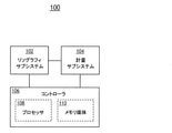
図1Aは、本開示の1個以上の実施形態による、半導体素子システム100を示す概念図である。一実施形態において、システム100は、試料上に1個以上のパターン(例:素子パターン、計量パターン等)をリソグラフィ的に印刷するリソグラフィサブシステム102を含んでいる。リソグラフィサブシステム102は、当分野で公知の任意のリソグラフィ印刷ツールを含んでいてよい。例えば、リソグラフィサブシステム102は、スキャナまたはステッパを含んでいるが、これらに限定されない。別の実施形態において、システム100は計量サブシステム104を含んでいる。例えば、計量サブシステム104は、試料上の1個以上の印刷パターンを特徴付けることができる。この点に関して、計量サブシステム104は、試料上での確率的反復因子の1回以上の発生を測定することができる。別の例として、計量サブシステム104は、パターンマスク(例:リソグラフィサブシステム102により試料上に露光される素子要素のパターンを含むパターンマスク)を特徴付けることができる。この点に関して、計量サブシステム104は、既知の製造レシピに従い形成される際に、加工欠陥の影響を受けやすい素子要素のパターンの1個以上の部分を測定することができる。一般的な意味で、計量サブシステム104は、当分野で公知の任意の方法を用いて、任意の計量尺度(例:オーバーレイ誤差、パターン配置誤差、試料特徴の寸法、臨界寸法(CD)、側壁角等)も測定することができる。一実施形態において、計量サブシステム104は、試料(例:ウェーハ、パターンマスク等)の1個以上の画像の生成に基づいて計量データを測定する画像利用計量ツールを含んでいる。別の実施形態において、計量サブシステム104は、試料(例:ウェーハ、パターンマスク等)から光の散乱(反射、回折、拡散散乱等)に基づいて計量データを測定する光波散乱計測に基づく計量システムを含んでいる。
FIG. 1A is a conceptual diagram showing a
別の実施形態において、システム100はコントローラ106を含んでいる。別の実施形態において、コントローラ106は、メモリ素子110に保持されたプログラム命令を実行すべく構成された1個以上のプロセッサ108を含んでいる。この点に関して、コントローラ106の1個以上のプロセッサ108は、本開示全体にわたり記述する各種の処理ステップのいずれかを実行することができる。例えば、コントローラ106は、確率的反復因子を識別すべくリソグラフィステップ(例:製造レシピに従いリソグラフィサブシステム102が実行するリソグラフィステップ)の1個以上の態様をシミュレートすることができる。別の例として、コントローラ106は、確率的反復因子を識別すべく計量サブシステム104からの計量データを解析および/または解釈することができる。
In another embodiment, the
コントローラ106の1個以上のプロセッサ108は、当分野で公知の任意の処理要素を含んでいてよい。この意味において、1個以上のプロセッサ108は、アルゴリズムおよび/または命令を実行すべく構成された任意のマイクロプロセッサ型の素子を含んでいてよい。一実施形態において、1個以上のプロセッサ108は、本開示全体にわたり記述するように、デスクトップコンピュータ、メインフレームコンピュータシステム、ワークステーション、画像コンピュータ、並列プロセッサ、またはシステム100を動作させるべく構成されたプログラムを実行すべく構成された他の任意のコンピュータシステム(例:ネットワークコンピュータ)を含んでいてよい。用語「プロセッサ」が、非一時的メモリ素子110からのプログラム命令を実行する1個以上の処理要素を有する任意の素子も含むように広義に定義されていてよいことを更に認識されたい。更に、本開示全体にわたり記述するステップは、単一のコントローラ106、または代替的に複数のコントローラにより実行されてよい。また、コントローラ106は、1個の共通筐体または複数の筐体内に収納された1個以上のコントローラを含んでいてよい。このように、任意のコントローラまたはコントローラの組み合わせが、システム100への組み込みに適した1個のモジュールとして別々にパッケージされていてよい。更に、コントローラ106は、検出器142から取得したデータを解析して、当該データを計量サブシステム104内の、またはシステム100の外部の追加的な要素に送ることができる。
One or
メモリ素子110は、対応付けられた1個以上のプロセッサ108により実行可能なプログラム命令の保存に適した当分野で公知の任意の記憶媒体を含んでいてよい。例えば、メモリ素子110は非一時的メモリ媒体を含んでいてよい。別の例として、メモリ素子110は、読出し専用メモリ、ランダムアクセスメモリ、磁気または光メモリ素子(例:ディスク)、磁気テープ、固体ドライブ等を含んでいてよいが、これらに限定されない。メモリ素子110が、1個以上のプロセッサ108と共通のコントローラ筐体に収納できることを更に注記しておく。一実施形態において、メモリ素子110は、1個以上のプロセッサ108およびコントローラ106の物理的位置に関して遠隔位置に配置されていてよい。例えば、コントローラ106の1個以上のプロセッサ108は、ネットワーク(例:インターネット、イントラネット等)を介してアクセス可能なリモートメモリ(例:サーバ)にアクセスすることができる。従って、上述の説明は、本発明を限定するものではなく、単に説明目的に過ぎないものと解釈されたい。
The
図1Bは、本開示の1個以上の実施形態による、リソグラフィサブシステム102を示す概念図である。一実施形態において、リソグラフィサブシステム102は、1個以上の照射光線114を生成すべく構成されたリソグラフィ照射光源112を含んでいる。1個以上の照射光線114は、紫外(UV)放射、可視放射、または赤外(IR)放射を含むがこれらに限定されない1個以上の選択された光の波長を含んでいてよい。
FIG. 1B is a conceptual diagram showing a
リソグラフィ照射光源112は、照射光線114の生成に適した当分野で公知の任意の種類の照射光源を含んでいてよい。例えば、リソグラフィ照射光源112は、1個以上のレーザーシステム(例:ガスレーザー、ダイオードレーザー、自由電子レーザー、ファイバレーザー、ディスクレーザー等)を含んでいてよい。別の例として、リソグラフィ照射光源112は、1個以上のランプシステム(例:アーク灯等)を含んでいてよい。別の例として、リソグラフィ照射光源112は、プラズマ照射光源(例:レーザーパルスプラズマ(LPP)光源、放電励起プラズマ(DPP)、レーザー維持プラズマ(LSP)等)を含んでいる。
The lithography irradiation
リソグラフィ照射光源112はまた、フィルタ、偏光子、波長板、または拡散器等の、但しこれらに限定されない照射ビーム114の1個以上態様の操作に適した任意の個数の光学要素を含んでいてよい。
The lithography irradiation
リソグラフィ照射光源112からの照射は任意の空間分布(例:照射パターン)を有していてよい。例えば、リソグラフィ照射光源112は、単極照射光源、双極照射光源、デカルト四極照射光源、クエーサー照射光源、または自由照射光源を含んでいてよいが、これらに限定されない。この点に関して、リソグラフィ照射光源112は、照射が、光軸116に沿って(または、平行に)伝播する軸上照射ビーム114および/または照射が光軸116に対してある角度で伝播する任意の個数の軸外照射ビーム114を生成することができる。
The irradiation from the lithography irradiation
別の実施形態において、リソグラフィサブシステム102はマスク支持素子118を含んでいる。マスク支持素子118は、加工中に露光される要素のパターンを含むパターンマスク120を固定すべく構成されている。別の実施形態において、リソグラフィサブシステム102は、1個以上の照射ビーム114により照射されたパターンマスク120の画像を、パターンマスク120の画像に対応する印刷パターン要素を生成すべく試料台126に配置されたリソグラフィ試料124上に射影すべく構成された射影光学機器の組122を含んでいる。別の実施形態において、マスク支持素子118は、パターンマスク120を移動または配置すべく構成されていてよい。例えば、マスク支持素子118は、システム100の射影光学機器122に関して選択された位置にパターンマスク120を移動させることができる。
In another embodiment, the
本開示全体にわたり用いる用語「リソグラフィ試料」は一般に半導体または非半導体材(例:ウェーハ、等)形成された基板に関する。例えば、半導体または非半導体材は、単結晶シリコン、ヒ化ガリウム、およびリン化インジウムを含んでいるが、これらに限定されない。本開示の目的のために、用語「リソグラフィ試料」と「ウェーハ」は互いに代替可能であると解釈されたい。 As used throughout this disclosure, the term "lithographic sample" generally relates to a substrate formed of a semiconductor or non-semiconductor material (eg, wafer, etc.). For example, semiconductor or non-semiconductor materials include, but are not limited to, single crystal silicon, gallium arsenide, and indium phosphide. For the purposes of this disclosure, the terms "lithographic sample" and "wafer" should be construed as interchangeable.
リソグラフィ試料124は、パターンマスク120の画像の取得に適した任意の個数の感光材料および/または材料層を含んでいてよい。例えば、リソグラフィ試料124はレジスト層128を含んでいてよい。この点に関して、射影光学機器の組122は、パターンマスク120の画像をレジスト層128上に射影してレジスト層128を露光して、リソグラフィ試料124の上に印刷特徴を形成すべく後続のエッチングステップにより露光された材料(例:正エッチング)または露光されていない材料(例:負エッチング)を除去する。更に、パターンマスク120は、当分野で公知の任意の結像構成に用いることができる。例えば、パターンマスク120は、パターン要素が印刷パターン要素として正に結像される正マスク(例:明視野マスク)であってよい。別の例として、パターンマスク120は、パターンマスク120のパターン要素が負印刷パターン要素(例:すきま、間隔等)を形成する負マスク(例:暗視野マスク)であってよい。
The
コントローラ106は、リソグラフィサブシステム102内の任意の個数の要素と通信可能に結合されていてよい。例えば、コントローラ106は、パターンマスク120上のパターン要素の露光をリソグラフィ試料124(例:試料上のレジスト層128等)に誘導すべく、マスク支持素子118、リソグラフィ照射光源112、および/または試料台126と通信可能に結合されていてよい。この点に関して、露光線量、リソグラフィサブシステム102内の試料の焦点位置等の露光条件を調整することができる。
The
図1Cは、本開示の1個以上の実施形態による、計量サブシステム104を示す概念図である。一実施形態において、計量サブシステム104は、計量照射ビーム132を生成する計量照射光源130を含んでいる。別の実施形態において、計量照射光源130はリソグラフィ照射光源112と同一である。更なる例において、計量照射光源130は、別個の計量照射ビーム132を生成すべく構成された別個の照射光源である。計量照射ビーム132は、紫外(UV)放射、可視放射、または赤外(IR)放射を含むがこれらに限定されない1個以上の選択された光の波長を含んでいてよい。
FIG. 1C is a conceptual diagram showing a
別の実施形態において、計量照射光源130は、照射経路134を介して計量照射ビーム132を計量試料125へ誘導する。本開示全体にわたり用いる用語「計量試料」は一般に計量サブシステム104により検査される対象を指す。例えば、計量試料125はリソグラフィ試料124を含んでいてよいが、必須ではない。この点に関して、計量サブシステム104はウェーハ検査システムとして動作可能である。別の例として、計量試料125は、パターンマスク(例:レチクル)を含んでいてよい。この点に関して、計量サブシステム104はレチクル検査システムとして動作可能である。
In another embodiment, the metered irradiation
照射経路134は、計量照射ビーム132の変更および/または調整に適した1個以上のレンズ136または追加的な光学機器138を含んでいてよい。例えば、1個以上の光学機器138は、1個以上の偏光子、1個以上のフィルタ、1個以上のビームスプリッタ、1個以上の拡散器、1個以上のホモジナイザ、1個以上のアポダイザ、または1個以上のビーム整形器を含んでいるが、これらに限定されない。別の実施形態において、計量サブシステム104は、計量照射ビーム132を計量試料125に集光させる対物レンズ140を含んでいる。
The
別の実施形態において、計量サブシステム104は、収集経路144を通って計量試料125から発せられた放射線を捕捉すべく構成された検出器142を含んでいる。例えば、検出器142は、収集経路144(例:対物レンズ140、レンズ146等)内の要素により提供されるリソグラフィ試料124の画像を取得することができる。別の例として、検出器142は、計量試料125から反射または散乱された(例:鏡面反射、拡散反射等を介して)放射を受けることができる。別の例として、検出器142は、計量試料125により生成(例:計量照射ビーム132の吸収に伴う発光等)された放射を受けることができる。別の例として、検出器142は、計量試料125からの1次以上の回析放射(例:0次回折、±1次回折、±2次回折等)を受けることができる。
In another embodiment, the
検出器142は、計量試料125から受けた照射の測定に適した当分野で公知の任意の種類の光学式検出器を含んでいてよい。例えば、検出器142は、CCD検出器、TDI検出器、光電子増倍管(PMT)、アバランシェフォトダイオード(APD)等を含んでいるが、これらに限定されない。別の実施形態において、検出器142は、計量試料125から発せられた放射の波長の識別に適した分光検出器を含んでいてよい。別の実施形態において、計量サブシステム104は、(例:計量サブシステム104により複数の計量測定(例:複数の計量ツール)を容易にすべく1個以上のビームスプリッタにより生成された複数の光路に関連付けられた)複数の検出器142を含んでいてよい。
The
収集経路144は更に、1個以上のレンズ146、1個以上のフィルタ、1個以上の偏光子、または1個以上のビームブロックを含むがこれらに限定されない対物レンズ140により収集された照射を誘導および/または変更する任意の個数の光学要素を含んでいてよい。
The
一実施形態において、図1Cに示すように、計量サブシステム104は、対物レンズ140が計量照射ビーム132を計量試料125に誘導し、同時に計量試料125から発せられた放射を収集できる向きに配置されたビームスプリッタ148を含んでいてよい。この点に関して、計量サブシステム104は、エピ照射モードに設定されていてよい。別の実施形態において、計量試料125への計量照射ビーム132の入射角は調整可能である。例えば、ビームスプリッタ148および対物レンズ140を通る計量照射ビーム132の経路は、計量試料125への計量照射ビーム132の入射角を制御すべく調整することができる。この点に関して、計量照射ビーム132は、計量照射ビーム132が計量試料125に垂直に入射するように、ビームスプリッタ126および対物レンズ14を通る名目経路を有していてよい。更に、計量試料125への計量照射ビーム132の入射角は、ビームスプリッタ148上での計量照射ビーム132の位置および/または角度を(例:回転ミラー、空間光変調器、自由照射光源等により)変更することにより制御することができる。別の実施形態において、計量照射光源130は、1個以上の計量照射ビーム132を、計量試料125に対してある角度(例:視射角、45度の角度等)で誘導する。
In one embodiment, as shown in FIG. 1C, the
別の実施形態において、計量サブシステム104は、システム100のコントローラ106と通信可能に結合されている。この点に関して、コントローラ106は、計量データ(例:計量測定結果、目標の画像、瞳孔画像等)または計量尺度(例:精度、ツールに起因するシフト、感度、回折効率、スルーフォーカス傾斜、側壁角、臨界寸法等)を含むがこれらに限定されないデータを取得すべく構成されていてよい。別の実施形態において、コントローラ106は、照射ビーム104と計量試料125との間の入射角の調整を誘導すべく計量照射光源130と通信可能に結合されている。別の実施形態において、コントローラ106は、照射の1個以上の選択された波長を(例:フィードバックに応答して)提供するよう計量照射光源130に指示する。
In another embodiment, the weighing
一般的な意味において、計量サブシステム104は、1個以上の照射角を有する分光エリプソメータ、ミュラー行列要素を(例:回転補正器を用いて)測定する分光エリプソメータ、単波長エリプソメータ、角度分解エリプソメータ(例:ビームプロファイルエリプソメータ)、分光反射率計、単波長反射率計、角度分解反射率計(例:ビームプロファイル反射率計)、結像システム、瞳孔結像システム、スペクトル結像システム、または散乱計等の当分野で公知の任意の種類の計量システムを含んでいてよいが、これらに限定されない。更に、計量システムは、単一の計量ツールまたは複数の計量ツールを含んでいてよい。複数の計量ツールが組み込まれた計量システムは米国特許第7,478,019号に一般的に記述されている。主として反射光学機器に基づく集光ビーム偏光解析法は米国特許第5,608,526号に一般的に記載されており、その全文を本明細書で引用している。幾何学的光学機器により規定されるサイズを越える照射点の広がりを生じさせる光回折の影響をアポダイザを用いて抑制することは米国特許第5,859,424番に一般的に記載されており、その全文を本明細書で引用している。複数の入射角での同時照射と共に高開口数ツールを用いることは米国特許第6,429,943号に一般的に記述されており、その全文を本明細書で引用している。高NA光リソグラフィにおける結像性能の定量化は、Lee他「Quantifying imaging performance bounds of extreme dipole illumination in high NA optical lithography」,Proc.of SPIE Vol.9985 99850X-1(2016)に記述されており、その全文を本明細書で引用している。
In a general sense, the
図2は、本開示の1個以上の実施形態による、確率性を仮定した計量方法200で実行されるステップを示すフロー図である。出願人は、システム100との関連で上述した実施形態および実行技術が方法200に拡張できるものと解釈すべきであることを注記する。しかし、方法200がシステム100のアーキテクチャに限定されないことも更に注記しておく。
FIG. 2 is a flow chart showing steps performed by the
一実施形態において、方法200は、試料上に形成される要素の少なくとも1個のパターン、および照射により要素のパターンを露光するための1個以上の露光パラメータを含む製造レシピを取得するステップ202を含んでいる。
In one embodiment,
試料(例:システム100のリソグラフィ試料124)の上に形成される要素のパターンは任意の種類の特徴を含んでいてよい。例えば、要素のパターンは、動作可能な半導体素子の一部として形成された特徴に対応する1個以上の素子要素、または1個以上の計量目標(例:1個以上のオーバーレイ目標、露光に敏感な1個以上の目標、試料の焦点位置に敏感な1個以上の目標等)を含んでいてよい。この点に関して、要素のパターンの任意の部分の確率的反復因子に対する感受性を特徴付けることができる。
The pattern of elements formed on the sample (eg,
更に、露光パラメータは、照射光源の波長、照射線量(例:試料に入射する単位面積当たりのエネルギー)、試料の焦点位置(例:リソグラフィサブシステム102内等)、露光時間、照射光源の空間プロファイル、または試料への照射の空間分布を含んでいるが、これらに限定されない。
Further, the exposure parameters include the wavelength of the irradiation light source, the irradiation dose (eg, energy per unit area incident on the sample), the focal position of the sample (eg, in the
一般的な意味において、製造レシピは、単一位置または複数位置から取得されてよい。例えば、製造レシピは、メモリ素子(例:メモリ素子に保存されたファイル)から取得されてよい。一例としてシステム100を挙げれば、製造レシピはコントローラ106によりメモリ素子110から取得されてよい。更に、製造レシピは、ローカルメモリ素子(例:コントローラ106と共通の筐体に格納された)、または遠隔メモリ素子(例:ネットワークを介してコントローラに接続されたレシピ管理システム等)から取得されてよい。また、製造レシピの各部分が異なる位置から取得されてもよい。例えば、試料上に形成される要素のパターンは、1個以上の層の特徴の幾何学的な配置、1個以上の層に関連付けられた材料特性、または1個以上の層の特徴間の電気的接続を含むがこれらに限定されない、メモリ素子に保存された素子設計ファイルに関連付けられていてよい。
In a general sense, manufacturing recipes may be obtained from a single position or multiple positions. For example, the manufacturing recipe may be obtained from a memory element (eg, a file stored in the memory element). Taking the
別の実施形態において、方法200は、製造レシピに従い形成される際に確率的変化(例:確率的反復因子)の影響を受けやすい要素のパターンの1個以上の候補保護領域を識別するステップ204を含んでいる。この点に関して、候補保護領域は、製造レシピに従い形成される際に、上述のように確率的に生じることが予測される加工欠陥を含んでいてよい。従って、候補保護領域は、1個以上の欠陥が確率的に生じ得る位置に対応していてよい。例えば、候補保護領域は、決定論的反復因子(例:同一位置での各加工工程で発生が予測される欠陥)に関連付けられた不具合点および確率的反復因子に影響されやすい識別された弱点の両方を含んでいてよい。識別された弱点は、仕様の範囲内ではあるが名目値から外れた要素のパターン(例:要素の特定のサイズまたは形状、特定要素間の距離等)内の特徴を含んでいてよい。
In another embodiment,
確率的反復因子の影響を受けやすい候補保護領域は、ウェーハ上で露光される要素のパターンを含むパターンマスク(例:レチクル)または何らかの製造ステップ(例:任意の層のADIまたはAEI)の後のウェーハに関連付けられていてよい。例えば、確率的反復因子の影響を受けやすいレチクル上の候補保護領域の識別は、ウェーハ加工前に補正処置(例:確率的欠陥の形成を抑制すべく製造レシピの変更、または確率的欠陥を監視すべく計量レシピの生成)を可能にすべく印刷チェック処理で利用することができる。別の例として、確率的反復因子の影響を受けやすいウェーハ上の候補保護領域の識別は、ホットスポット識別、PWG解析、またはWET解析を含むがこれらに限定されない任意の処理監視アプリケーションでも利用することができる。 Candidate protection areas susceptible to stochastic iteration factors are after a pattern mask (eg, reticle) containing a pattern of elements exposed on the wafer or some manufacturing step (eg, ADI or AEI of any layer). It may be associated with a wafer. For example, identification of candidate protected areas on a reticle susceptible to stochastic repeat factors is a corrective action prior to wafer machining (eg, manufacturing recipe changes to suppress the formation of stochastic defects, or monitoring of stochastic defects. It can be used in the print check process to enable the generation of weighing recipes). As another example, identification of candidate protected areas on wafers susceptible to stochastic iteration factors can also be used in any processing monitoring application including, but not limited to, hotspot identification, PWG analysis, or WET analysis. Can be done.
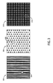
ステップ204で識別された候補保護領域は、当分野で公知の任意の種類の予測される確率的反復因子を含んでいてよい。図3は、本開示の1個以上の実施形態による加工済み試料上の確率的反復因子の概念的イラストを含んでいる。例えば、イラスト302はライン-間隔パターンを含んでいて、加工処理の確率的変化は、確率的反復因子304等のライン-間隔パターンの要素間に不規則且つ不要な接続(例:電気的短絡等)に至る恐れがある。別の例として、イラスト306は孔の周期的分布を含んでいる。本例において、イラスト306内の各孔は共通の半径を有する円形孔として設計されているが、加工処理における確率的変化により、形成された孔のサイズまたは形状が変化し得る。確率的反復因子308は、部分的に満たされた孔を含んでいる。別の例として、イラスト310は、円形プロファイルおよび共通の半径を有するように意図された列の周期的分布を含んでいる。本例において、加工処理における確率的変化により、形成された列のサイズまたは形状が変化する、または確率的反復因子312が示す隣接列間に不要な接続が生じる恐れがある。図3に示す例および関連する記述は説明目的に過ぎず、如何なる場合も本開示を限定するものと解釈すべきではないことを理解されたい。例えば、確率的反復因子は、エッジの周辺で吸収されたエネルギーの不確実性に伴う特徴エッジの配置および/または粗さの変化、および吸収されたエネルギーに対するエッジ位置の感度を含んでいてよい。別の例として、確率的反復因子は、ライン/間隔または先端間構造における架橋欠陥(例:ナノ架橋、マイクロ架橋等)を含んでいてよい。一般的な意味において、確率的反復因子は、加工中に確率的に現れる任意の種類の加工欠陥を含んでいてよい。
The candidate protected area identified in
確率的反復因子には、加工処理に伴う任意の個数の根本原因があり得る。例えば、所与の体積の試料(例:レジスト層)内における光子の吸収に伴う不確実性を光子衝突ノイズ(PSN)により特徴付けることができる。
![]()
![]()
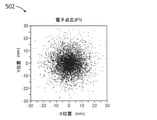
式1は更に、試料へのエネルギー量(例:照射光源の強度および/または出力に関連付けられた)を減らすことで更にPSNが増大し、従って確率的反復因子の尤度が増大し得ることを示している。特に大量生産環境において、指定された許容範囲(例:加工される構造の寸法および間隔の許容範囲、許される欠陥個数の許容範囲等)に従い望ましい構造の加工に充分な線量を維持しながら、試料への照射線量を可能な限り減少させることが典型的に望ましい。このように照射線量を最小化することで大量生産に際して、試料毎に必要な露光時間の短縮によるスループットの向上およびコスト減少等、但しこれらに限定されない複数の利点が得られる。本明細書において照射光源、特にEUV照射光源がエネルギー需要に伴う高い運用コストおよび維持コストを有し得ることが分かる。この点に関して、照射線量の減少による利点と、確率的反復因子の増大等、照射線量の減少による負の影響との間のバランスを取る照射線量を選択することが典型的に望ましい。本明細書において更に、露光ステップ(例:リソグラフィサブシステム102等における)実行中の試料の焦点位置がPSNに影響し得ることが分かる。例えば、名目焦点位置からの試料の焦点位置の変化により、パターンマスクから試料への結像パターン要素に関連付けられた不鮮明さ(例:リソグラフィサブシステム102の点広がり関数のサイズおよび/または形状の変化)が増す場合がある。従って、試料の焦点位置の変化が試料上の光子密度を変化させてPSNに影響を及ぼす恐れがある。
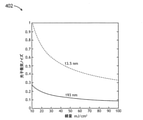
図4は、本開示の1個以上の実施形態による、フォトレジストの3nmの立方体内への照射の吸収に伴い、波長が193nm(例:ArF照射光源により生成)および13.5nm(例:EUV照射光源を用いて生成)の線量の関数として計算されたPSNを示すプロット図402である。図4に示す両方の照射波長において、試料への線量の減少はPSNの増大につながる。しかしこの傾向は、193nmの照射と比較して13.5nmの照射に線量の減らした場合にPSNがより大幅に増大することで示されるように、照射波長が短いほど顕著である。従って、より小さい特徴の加工を可能にすべく照射波長を短縮する場合、照射線量の決定に際して確率的反復因子をより重視することが求められる。 FIG. 4 shows wavelengths of 193 nm (eg, produced by an ArF irradiation light source) and 13.5 nm (eg, EUV) as the photoresist absorbs irradiation into a 3 nm cube according to one or more embodiments of the present disclosure. FIG. 402 is a plot diagram 402 showing PSN calculated as a function of dose (generated using an irradiation light source). At both irradiation wavelengths shown in FIG. 4, a decrease in the dose to the sample leads to an increase in PSN. However, this tendency is more pronounced with shorter irradiation wavelengths, as shown by the greater increase in PSN when the dose is reduced to 13.5 nm irradiation compared to 193 nm irradiation. Therefore, when shortening the irradiation wavelength to enable processing of smaller features, it is required to place more emphasis on the stochastic repeat factor when determining the irradiation dose.
確率的反復因子の追加的な根本原因は、フォトレジスト(例:レジスト層128等)内の確率的変化に絡んでいる場合がある。例えば、フォトレジストは、入射照射を吸収する光酸発生剤(PAG)を含んでいてよく、吸収されたエネルギーの量に対応する露光領域の可溶性を変化させる。この点に関して、フォトレジストの露光および非露光領域の可溶性が異なっていてよく、後続のエッチングステップで露光または非露光領域を選択的に除去して試料上の特徴を現像することができる。典型的に、PAGはフォトレジスト全体にわたり連続的ではなく、フォトレジスト全体にわたり分布する分子を含んでいる。従って、形成される特徴のサイズが小さくなるに従い、PAG分子の実際の位置の変化の影響が増大し、PAG分子に関連付けられた確率的反復因子が相応に増大する場合がある。
An additional root cause of the stochastic repeat factor may be associated with stochastic changes within the photoresist (eg, resist
更に、入射光子に対する酸の最終分布(例:変更された可溶性の分布)は、試料内における電子イオン化に起因して確率的変化を示す場合がある。特に、フォトレジストのイオン化閾値を超える光子エネルギーを有する光子が、光電効果に基づいてエネルギーを変化させる電子カスケードを誘導する場合がある。当該電子カスケードは次いでエネルギーに応じて異なる仕方でPAGと相互作用して更に可溶性に影響を及ぼす場合がある。従って、複数個の酸性分子が単一光子に反応してPAGにより生成される場合がある(例:酸の収率1より大きくてよい)。典型的に、フォトレジスト材料は、UVまたはEUV範囲にイオン化閾値を有しているため、当該UVまたはEUV範囲内の照射波長において電子イオン化の影響が顕著に現れて、吸収エネルギーが空間的に不鮮明になる恐れがある。 In addition, the final distribution of acids to incident photons (eg, altered soluble distribution) may show stochastic changes due to electron ionization within the sample. In particular, photons having photon energy that exceeds the ionization threshold of the photoresist may induce an electron cascade that changes the energy based on the photoelectric effect. The electron cascade may then interact with PAG in different ways depending on the energy to further affect solubility. Therefore, a plurality of acidic molecules may react with a single photon to be produced by PAG (eg, the acid yield may be greater than 1). Typically, the photoresist material has an ionization threshold in the UV or EUV range, so that the effect of electron ionization is noticeable at irradiation wavelengths within the UV or EUV range, and the absorption energy is spatially unclear. There is a risk of becoming.
図5Aは、本開示の1個以上の実施形態による、複数の制御された離散的光子吸収事象の物理的シミュレーションに基づく波長124nm(10eV)の照射に対するフォトレジスト内においてシミュレートされた電子点広がりのプロット図502である。図5Aで明らかに分かるように、フォトレジスト内の電子のイオン化に伴う電子散乱が、材料内で吸収されたエネルギーの再分布または不鮮明さを引き起こす恐れがある。ここで、エネルギーは少なくとも60nmの領域全体にわたり分布しているにも拘わらず、エネルギーは10~20nmの領域に極めて集中している。図5Bは、本開示の1個以上の実施形態による、図5Aに示す電子散乱の影響を含む波長124nm(10eV)の照射に対するフォトレジストの酸点広がりのプロット図504である。光子または電子のいずれかの吸収を通じてPAG分子により生じた酸の濃度は、図5Aの電子点広がりと同様の分布を示すが、全ての単一のイオン化された電子が酸性分子を生じるとは限らない(例:いくつかの電子は熱的に吸収される場合がある等)ため、酸の点広がりの寸法は僅かに小さくなる。上述のように、酸性分子の点広がりはフォトレジスト内の確率的変化を増大させ、確率的反復因子の増大に至る場合がある。また、照射波長を更に短縮することで更なる確率的変化が生じる場合がある。 FIG. 5A shows electron point spread simulated in a photoresist for irradiation at a wavelength of 124 nm (10 eV) based on physical simulation of multiple controlled discrete photon absorption events according to one or more embodiments of the present disclosure. It is a plot diagram 502 of. As is clearly shown in FIG. 5A, electron scattering associated with ionization of electrons in the photoresist can cause redistribution or blurring of the absorbed energy in the material. Here, although the energy is distributed over the entire region of at least 60 nm, the energy is extremely concentrated in the region of 10 to 20 nm. FIG. 5B is a plot of acid point spread of the photoresist to irradiation at a wavelength of 124 nm (10 eV) including the effects of electron scattering shown in FIG. 5A, according to one or more embodiments of the present disclosure. The concentration of acid produced by the PAG molecule through absorption of either a photon or an electron shows a distribution similar to the electron point spread in FIG. 5A, but not all single ionized electrons produce an acidic molecule. Since there are no (eg, some electrons may be thermally absorbed, etc.), the size of the acid point spread is slightly smaller. As mentioned above, the point spread of acidic molecules increases the stochastic changes in the photoresist, which can lead to an increase in stochastic repeat factors. Further, by further shortening the irradiation wavelength, a further stochastic change may occur.
更に、フォトレジスト内におけるPAG分子の濃度(例:PAG負荷)、および製造レシピの露光条件(例:照射線量および露光時間)の両方が更に確率的反復因子の生成に影響を及ぼす場合がある。図6Aは、本開示の1個以上の実施形態による、1個の光子吸収の1000回のシミュレーションに対するフォトレジスト内のシミュレートされた電子点広がりのプロット図602である。図6Bは、本開示の1個以上の実施形態による、1000個の光子の吸収の1回のシミュレーションに対するフォトレジスト内の電子点広がりのプロット図604である。表1は、両方のシミュレーションにおける電子散乱データを含んでいる。
In addition, both the concentration of PAG molecules in the photoresist (eg, PAG loading) and the exposure conditions of the recipe (eg, irradiation dose and exposure time) may further affect the generation of probabilistic repeat factors. FIG. 6A is a plot of simulated electron point spreads in a photoresist for 1000 simulations of one photon absorption according to one or more embodiments of the present disclosure. FIG. 6B is a

吸収されたエネルギーの総量は両方のシミュレーションで同一である。しかし、プロット図602のシミュレーションは低出力、長時間露光製造レシピを表すのに対し、プロット図604のシミュレーションは高線量、短露光時間製造レシピを表す場合がある。更に、電子散乱特徴(例:吸収位置からの電子移動距離、従ってエネルギー再分布の空間範囲)は低出力と高出力露光とで異なる場合がある。特に、高出力露光は低線量露光よりも多い個数のイオン化電子を生成する場合がある。更に、エネルギー再分布の空間範囲は、高出力照射、特に最大電子距離で顕著に大きい場合がある。この点に関して、高出力照射は、吸収されたエネルギーの再分布または不鮮明さの長さがより大きいため、低出力照射と比較して加工時の確率的変化、従って確率的反復因子の影響をより受けやすい。吸収されたエネルギーの過度な不鮮明さは、射影された光学画像のコントラストの喪失または低下を表す場合がある。
The total amount of energy absorbed is the same in both simulations. However, while the simulation in
別の実施形態において、ステップ204は、試料上でのパターン要素の形成をシミュレートすることにより候補保護領域を識別するステップを含んでいる。ステップ204は、各種のアルゴリズムにより確率的計算リソグラフィを用いて候補保護領域を識別するステップを含んでいてよい。例えば、入射照射(例:照射ビーム114等)と試料(例:リソグラフィ試料124等)の光相互作用を、電磁気(EM)ソルバーを用いてモデル化することができる。更に、EMソルバーは、厳密結合波解析(RCWA)、有限要素法解析、モーメント解析方法、面積分法、体積分法、または有限差分時間領域解析を含むがこれらに限定されない当分野で公知の任意の方法を用いてよい。別の例として、入射照射と試料の光相互作用は、モンテカルロ法を用いてモデル化することができる。確率的シミュレーションは、試料による光子の吸収に伴う不確実性、試料内におけるPAGの分布、または上述のような試料内におけるイオン化に起因するエネルギー再分布等の、但しこれらに限定されない確率的プロセスの影響を特徴付けることができる。例えば、計算リソグラフィシミュレーションは、KLA-TENCOR社から提供されるPROLITHソフトウェア製品により実行されてよいが、必須ではない。
In another embodiment,
別の実施形態において、ステップ204は、確率的反復因子の影響を受けやすい領域を決定すべく製造レシピの要素パターンの設計を解析することにより候補保護領域を識別するステップを含んでいる。例えば、ステップ204は、エッジの周辺におけるエネルギー吸収の不確実性および吸収されたエネルギーに対するエッジの配置の感度の特徴付けに基づいて要素のパターン内におけるエッジの配置のシミュレーション(例:エッジの粗さ)含んでいてよい。この点に関して、エッジの粗さのシミュレーションは、確率的欠陥に対する広範な特徴(例:ライン-間隔特徴、孔または列)の影響の受けやすさを示唆するものである。エッジの周辺におけるエネルギー吸収の不確実性の計算は、PSN等の、但しこれらに限定されない任意の個数の要因に基づいていてよい。更に、エネルギー吸収に対するエッジ配置の感度の計算は、パターン要素のジオメトリ(例:湾曲の程度、鋭いエッジ等)、PAG負荷、または電子イオン化等の、但しこれらに限定されない任意の個数の要因に基づいていてよい。本明細書において、要素パターンの設計の解析が、より厳密な計算リソグラフィ解析よりも計算量が少ない、より高速のシミュレーションであってよいが、必須ではないことを理解されたい。従って、ステップ204は、精度と計算要件との所望のバランスに応じて、上述のような高速シミュレーションアルゴリズム、より厳密なシミュレーションアルゴリズム、またはアルゴリズムの組み合わせを含んでいてよい。
In another embodiment,
ステップ204は、確率的シミュレーションおよび/または要素パターンの設計の解析を用いて候補保護領域を識別すための任意の個数の入力を含んでいてよい。例えば、要素パターンの設計は、ステップ202で取得した設計ファイル内に含まれていてよいが、必須ではない。
Step 204 may include any number of inputs for identifying candidate protected areas using probabilistic simulations and / or analysis of element pattern designs. For example, the design of the element pattern may be included in the design file acquired in
また、ステップ204の入力は、フォトレジスト内での2また3次元の放射照度分布の表現を含んでいてよい。この放射照度分布は、シミュレーションおよび/または測定を介して得られる場合がある。例えば、入力は、試料層の膜厚および屈折率の実/虚部等、試料層の材料パラメータを含んでいるが、これらに限定されない。別の例として、入力は、照射プロファイル(例:光源形状、開口数、フレア等)の表現を含んでいてよい。別の例として、入力は、パターンマスクレイアウト(例:光近接効果補正構造、サブ解像度補助特徴等を含む)および3Dマスクスタックを含んでいてよい。
Also, the input in
更に、ステップ204の入力は、フォトレジスト内における放射照度分布に適用される加工システムに付随する処理時の不鮮明さの近似値を含んでいてよい。例えば、処理時の不鮮明さは、一定のガウス畳み込み核または線量依存の不鮮明さの形で現れる場合がある。
Further, the input in
別の実施形態において、ステップ204は、確率的反復因子の影響を受けやすい領域を決定すべく(例:計量サブシステム104等を用いて)1個以上の試料を検査することにより候補保護領域を識別するステップを含んでいる。例えば、ステップ204は、ウェーハに印刷された際に確率的欠陥が生じる恐れがあるパターンマスク上の要素のパターンの部分を識別すべくパターンマスク(例:レチクル)を検査するステップを含んでいてよい。この点に関して、候補保護領域は、決定論的な欠陥を生じるとは思われないが、名目設計から逸脱する恐れがあり、従って選択された露光条件で印刷された際に確率的欠陥に影響されやすいパターンマスクの部分を含んでいてよい。別の例として、ステップ204は、選択された仕様(例:臨界寸法、側壁角等)の範囲内で印刷されるが名目設計値から逸脱する恐れがある領域であって、複数の印刷ステップにわたり確率的変化に影響されやすい領域を識別すべく1個以上の印刷ウェーハを検査するステップを含んでいてよい。
In another embodiment,
別の実施形態において、方法200は、1個以上の確率的反復因子の1個以上の予測尤度を欠陥尤度閾値と比較することにより、1個以上の候補保護領域から1個以上の保護領域を選択するステップ206を含んでいる。上述のように、ステップ204で識別された候補保護領域、従ってステップ206で選択された保護領域は、加工処理の任意の時点(例:ADI、AEI等)でパターンマスクおよび/またはウェーハに関連付けられてよい。特定のパターン要素に関連付けられた確率的反復因子は、任意の確率分布(例:ポアソン分布、ガウス分布等)に従い、試料上の位置の関数として、または加工工程数の関数として生じる場合がある。ステップ206は従って、候補保護領域の確率的反復因子の確率を予測すべく、ステップ204で識別された各々の候補保護領域を解析するステップを含んでいてよい。更に、ステップ206は、欠陥尤度閾値に基づいて保護領域を選択するステップを含んでいてよい。欠陥尤度閾値は、任意の尺度に基づく確率的反復因子の閾値確率を含んでいてよい。例えば、ステップ206は、選択された製造レシピに従い加工(例:リソグラフィサブシステム102内の線量、照射プロファイル、焦点位置を含む選択された露光条件で加工)された際に、製造工程の選択された割合(例:50%、10%、1%、0.1%、0.001%等)で印刷されることが予測される欠陥を含む保護領域を選択するステップを含んでいてよい。
In another embodiment,
例示的な例として、特定のパターン要素が欠陥を伴い形成される確率が線量の関数としてポアソン分布をなしている場合がある。従って、パターン要素は、線量が充分に低い場合は露光が不充分なため、ほぼ常時欠陥(例:決定論的反復因子)を伴い印刷される恐れがある。同様に、パターン要素は、線量が充分高い場合は露光が充分であるため、欠陥を伴い印刷されることはほぼ無い。しかし、欠陥は、これらの極端なケース間の線量値の特定の範囲にわたり確率的に印刷し得るため、確率的反復因子であり得る。ステップ206は従って、選択された線量で加工された際に確率的反復因子の欠陥尤度閾値確率に基づいてステップ204で識別された候補保護領域から1個以上の保護領域を選択するステップを含んでいてよい。
As an exemplary example, the probability that a particular pattern element is formed with defects may have a Poisson distribution as a function of dose. Therefore, pattern elements may be printed almost always with defects (eg, deterministic repeat factors) due to insufficient exposure when the dose is low enough. Similarly, pattern elements are rarely printed with defects because exposure is sufficient when the dose is high enough. However, defects can be stochastic repeaters because they can be stochastically printed over a specific range of dose values between these extreme cases. Step 206 therefore comprises selecting one or more protected areas from the candidate protected areas identified in
上述の線量に依存する確率的反復因子の例が単に説明目的で挙げられているに過ぎず、本発明を限定するものと解釈すべきでないことを理解されたい。一般的な意味において、欠陥が印刷され得る確率は、広範な露光条件(例:線量、照射プロファイル、リソグラフィサブシステム102内の焦点位置等)により影響され得る。従って、ステップ206は、選択された露光条件の組に従い加工された際に確率的反復因子の欠陥尤度閾値確率に基づいて1個以上の保護領域を選択するステップを含んでいてよい。
It should be understood that the above examples of dose-dependent stochastic repeat factors are given for illustration purposes only and should not be construed as limiting the invention. In a general sense, the probability that a defect may be printed can be influenced by a wide range of exposure conditions (eg, dose, irradiation profile, focal position within the
候補保護領域が1個以上の欠陥(例:確率的反復因子の尤度)を伴い印刷される確率は、ステップ206において当分野で公知の任意の技術を用いて予測することができる。一実施形態において、候補保護領域内における確率的反復因子の尤度は、確率的シミュレーション(例:EMソルバーが組み込まれた確率的計算リソグラフィ、モンテカルロ法、パターン要素の設計の解析等)を用いて製造レシピに従い候補保護領域の構成をシミュレートすることにより測定される。
The probability that a candidate protected area will be printed with one or more defects (eg, the likelihood of a stochastic repeat factor) can be predicted in
例えば、ステップ204は比較的速いシミュレーション技術(例:上述の要素パターンの設計の解析)により候補保護領域を識別するステップを含んでいてよく、ステップ206はより厳密なシミュレーション技術(例:計算リソグラフィシミュレーション等)に基づいて候補保護領域から保護領域を選択するステップを含んでいてよい。この点に関して、ステップ204の比較的速いシミュレーション技術により計算負荷を減らし、従ってステップ206でより厳密なシミュレーションのスループットを向上させることができる。別の例として、ステップ204は1個以上の加工済み試料(例:ウェーハに印刷される要素のパターンを含むパターンマスク、印刷ウェーハ等)を検査することにより候補保護領域を識別するステップを含んでいてよく、ステップ206は計量に基づいて識別された候補保護領域の確率的シミュレーションに基づいて候補保護領域から保護領域を選択するステップを含んでいてよい。この点に関して、シミュレーションから、実際の加工処理に基づいて弱点(例:仕様内で印刷できるが名目値から外れている恐れがあるパターン)として識別される確率的反復因子の尤度を洞察することができる。
For example, step 204 may include a step of identifying candidate protected areas by a relatively fast simulation technique (eg, analysis of the element pattern design described above), and step 206 may include a more stringent simulation technique (eg, computational lithography simulation). Etc.) may include a step of selecting a protected area from candidate protected areas. In this regard, the relatively fast simulation technique of
別の実施形態において、候補保護領域内における確率的反復因子の形成確率は、ステップ204において確率的反復因子の予測尤度を決定すべく1個以上の印刷ウェーハ上で識別される候補保護領域を検査することにより決定される。例えば、ステップ204は確率的シミュレーション(例:上述の比較的速いシミュレーションおよび/または比較的厳密なシミュレーション)に基づいて候補保護領域を識別するステップを含んでいてよく、ステップ206は製造レシピに従い形成された1個以上のウェーハ上での識別された候補保護領域の検査に基づいて保護領域を選択するステップを含んでいてよい。この点に関して、ステップ204は、ステップ206でのウェーハの物理的検査(例:リソグラフィサブシステム102等による)を誘導するシミュレーションを含んでいてよい。更に、ステップ206は、確率的反復因子の尤度を最小化すべく設計された、ある範囲の露光条件(例:線量、焦点位置、照射プロファイル等)またはある範囲のパターン要素変更(例:変化光学パラメータ訂正(OPC)、サブ解像度補助特徴(SRAF)等)により一連のウェーハを加工するステップを含んでいてよい。従って、ステップ206は、確率的反復因子の尤度を予測すべく複数の製造レシピに従い形成された候補保護領域の検査を含んでいてよい。
In another embodiment, the probability of formation of a stochastic repeat factor within a candidate protected region is a candidate protected region identified on one or more printed wafers to determine the predictive likelihood of the stochastic repeat factor in
別の実施形態において、候補保護領域内における確率的反復因子の確率は、当該候補保護領域内における要素の配置を、確率的反復因子の尤度を予測したパターンレイアウトのライブラリと比較することにより決定される。従って、候補保護領域内における確率的反復因子の確率を、加工済み試料のシミュレーションおよび/または測定により生成可能な、但し生成は必須でない、訓練データとの比較に基づいて解析することができる。例えば、候補保護領域は、ライブラリ、高速低減次数モデル、回帰、深層学習技術等の機械学習アルゴリズム、ニューラルネットワーク、サポートベクトルマシン(SVM)、次元削減アルゴリズム(例:主成分分析(PCA)、独立成分分析(ICA)、局所線形埋め込み(LLE)等)、データの疎表現(例:フーリエまたはウェーブレット変換、カルマンフィルタ、同一または異種ツールからのマッチングを促進するアルゴリズム等)を含むがこれらに限定されないデータフィッティングおよび最適化技術を用いて解析することができる。候補保護領域解析は、KLA-TENCOR社から提供される「Signal Response Metrology(SRM)」ソフトウェア製品により実行されてよいが、実行は必須ではない。また、候補保護領域データは、設計ファイルからのパターン要素の設計、加工済み試料(例:パターンマスクまたはウェーハ)のシミュレーションまたは物理的検査等、但しこれらに限定されない任意の出所から提供されてよい。 In another embodiment, the probability of a stochastic repeat factor within a candidate protected region is determined by comparing the placement of elements within the candidate protected region with a library of pattern layouts that predict the likelihood of the stochastic repeat factor. Will be done. Therefore, the probabilities of probabilistic repeat factors within the candidate protected region can be analyzed based on comparisons with training data that can be generated by simulation and / or measurement of the processed sample, but generation is not essential. For example, candidate protection regions include libraries, fast reduction order models, regression, machine learning algorithms such as deep learning techniques, neural networks, support vector machines (SVMs), dimensionality reduction algorithms (eg principal component analysis (PCA), independent components). Data fitting including, but not limited to, analysis (ICA), local linear embedding (LLE), etc.), sparse representation of data (eg, Fourier or wavelet transformations, Kalman filters, algorithms that facilitate matching from identical or heterogeneous tools, etc.) And can be analyzed using optimization techniques. Candidate protected area analysis may be performed by the "Signal Response Metrology (SRM)" software product provided by KLA-TENCOR, but is not required. Also, candidate protected area data may be provided from any source, such as, but not limited to, designing pattern elements from a design file, simulating or physically inspecting a processed sample (eg, pattern mask or wafer).
別の実施形態において、ステップ204で識別された候補保護領域および/またはステップ206で選択された保護領域は、確率的反復因子の尤度を予測したパターンレイアウトのライブラリに挿入することができる。この点に関して、ライブラリは、確率的シミュレーション、計量結果、および/または計量により検証されたシミュレーションにより更新および/または訓練することができる。
In another embodiment, the candidate protected area identified in
別の実施形態において、ステップ206は、予測される欠陥尤度に基づいて1個以上の候補保護領内で見出された確率的反復因子を試料上での位置の関数としてランク付けするステップを含んでいる。特定のパターンが欠陥と共に(例:確率的反復因子として)形成される尤度が試料上の位置に基づいて変化し得ることを認識されたい。特定のパターンは試料上の特定の位置でのみ印刷品質が低い(欠陥の確率が高い)のに対し、他のパターンは試料上のほほ全ての位置で印刷品質が低い場合がある。従って、確率的反復因子の試料の位置の関数としてのランキングに関連付けられたデータを、計量システムが確率的反復因子を高感度で監視するようにサンプリング計画を生成すべく提供(例:フィードフォワードデータとして)する場合がある。
In another embodiment,
別の実施形態において、ステップ206で選択された保護領域は、確率的シミュレーションモデル(例:ステップ204および/またはステップ206で用いた確率的シミュレーションモデル)を改良および/または訓練すべくフィードバックして予測精度および/または効率を向上させることができる。従って、要素パターン形成のシミュレーションと、同一条件下で形成されたパターン要素の検査との組み合わせに基づいて保護領域を選択することで、確率的シミュレーションモデルを常に改良すべく反復的フィードバックを提供することができる。
In another embodiment, the protected area selected in
別の実施形態において、ステップ206で選択された保護領域を用いて計量レシピ(例:計量サブシステム104等により用いられる)を生成することができる。当該計量レシピが、試料で上の選択された個数の代表的な位置での加工中に試料の1個以上の態様を特徴付けるべく(例:欠陥の監視、層間オーバーレイの監視等に)作成されたサンプリング計画を含んでいてよいことが分かる。サンプリング計画の個数および特定の位置は典型的に、精度とスループットのバランスに基づいていてよい。しかし、決定論的な反復因子(例:ほぼ全ての製造工程内の所与の位置で定常的に生じる欠陥)を特徴付けるべく作成されたサンプリング計画が、試料の異なる位置において異なる確率で生じる場合がある確率的反復因子を特徴付けるのには適していないことが更に分かる。一実施形態において、ステップ206で選択された保護領域を用いて、製造処理の任意の段階で確率的反復因子を監視するのに適したウェーハ上での検査対象位置を含むサンプリング計画を生成する。例えば、本明細書に示す発明的概念に従い作成されたサンプリング計画は、加工中に確率的反復因子を高感度且つ効果的に監視できるよう各種の確率的反復因子の確率を位置の関数として組み込むことができる。
In another embodiment, the protected area selected in
更に、確率的反復因子を含む保護領域に関連付けられたデータ(例:保護領域の位置、保護領域内における確率的反復因子の確率等)は、製造ラインの所与の追加的なツール(例:フィードフォワードデータとしての)であってよい。例えば、保護領域は、サンプリング計画に従い1個以上の試料(例:レチクルおよび/またはウェーハ)を測定する所与の計量ツールに提供されてよい。追加的な例として、確率的反復因子を含む保護領域に関連付けられたデータは、処理エラー、ウェーハ汚染等に起因する欠陥(例:決定論的および/または確率的欠陥)の影響を受けやすいウェーハの部分を識別すべくホットスポット検証ツールに提供されてよい。 In addition, the data associated with the protected area containing the probabilistic repeat factor (eg, location of the protected area, probability of the stochastic repeat factor within the protected area, etc.) can be used as an additional tool on the production line (eg, example). It may be (as feedforward data). For example, the protected area may be provided to a given weighing tool that measures one or more samples (eg, reticle and / or wafer) according to a sampling scheme. As an additional example, the data associated with the protected area containing stochastic repeat factors is susceptible to defects due to processing errors, wafer contamination, etc. (eg, deterministic and / or stochastic defects). It may be provided to a hotspot verification tool to identify the part of.
別の実施形態において、方法200は、1個以上の保護領域内における1個以上の確率的反復因子の予測される生起を選択された許容範囲内に抑制すべく製造レシピを変更するステップ208を含んでいる。これは、許容可能な個数の欠陥(確率的反復因子および/または決定論的反復因子)を規定する選択された許容範囲内で特定の素子が形成される場合であってもよい。従って、ステップ208は、確率的反復因子を考慮に入れた場合に当該素子が選択された許容範囲に従い形成できるように製造レシピの少なくとも1個の態様を変更するステップを含んでいてよい。
In another embodiment,
一実施形態において、製造レシピを変更するステップは、確率的反復因子を抑制すべく1個以上の露光条件(例:リソグラフィサブシステム102の線量、焦点位置、照射条件等)を変更するステップを含んでいる。例えば、ステップ208は、確率的反復因子の尤度を選択された許容範囲まで減らすべく試料(例:ステップ206で選択された保護領域に関連付けられた)の1個以上の部分への照射線量を増やすステップを含んでいてよい。
In one embodiment, the step of changing the manufacturing recipe comprises changing one or more exposure conditions (eg, dose, focal position, irradiation conditions, etc. of the lithography subsystem 102) in order to suppress stochastic repeat factors. I'm out. For example,
別の実施形態において、製造レシピを変更するステップは、確率的反復因子を抑制すべく形成される要素のパターンを変更するステップを含んでいる。例えば、要素パターン内の1個以上の特徴は、確率的反復因子に影響され難い他のパターンレイアウトに変更および/または代替することができる。大艇的なパターンレイアウトは、当分野で公知の任意の技術を用いて選択することができる。例えば、代替的なパターンレイアウトは、確率的反復因子に対する既知の影響されやすさによるパターンレイアウトのライブラリの確率的ランキングに基づいて選択することができる。別の例として、パターンマスクは、リソグラフィ試料124上の要素のパターンの印刷可能性を向上させるのに適したサブ解像度特徴(OPC特徴、SRAF等)を含むように変更することができる。この点に関して、リソグラフィサブシステム102の解像度よりも寸法(例:実際の寸法、パターンマスク要素同士の間隔等)が小さいパターンマスク素子は、散乱または回折等の光学的効果に基づいて試料のレジスト層上に印刷されるパターンに影響する場合がある。例えば、サブ解像度特徴は、リソグラフィ試料124上へ解像可能に結像されることなく、印刷要素の1個以上の特徴(例:PPE、側壁角、臨界寸法等)に影響する場合がある。更に、サブ解像度特徴は、選択された許容範囲(例:プロセスウィンドウ)内で要素のパターンを形成できる露光条件の範囲に影響する場合がある。この点に関して、サブ解像度特徴は、サブ解像度要素自体が解像可能に印刷されることなく要素の設計されたパターンをリソグラフィ試料124上に確実に形成可能にすることができる。
In another embodiment, the step of modifying the manufacturing recipe comprises the step of altering the pattern of the elements formed to suppress the stochastic repeat factor. For example, one or more features within an element pattern can be modified and / or replaced with other pattern layouts that are less susceptible to stochastic iteration factors. The boat-like pattern layout can be selected using any technique known in the art. For example, alternative pattern layouts can be selected based on the probabilistic ranking of a library of pattern layouts based on known susceptibility to probabilistic iteration factors. As another example, the pattern mask can be modified to include sub-resolution features (OPC features, SRAF, etc.) suitable for improving the printability of the pattern of elements on the
別の実施形態において、方法200は、変更された製造レシピに従い少なくとも1個の試料を加工するステップ210を含んでいる。従って、任意の確率的反復因子を特徴付けることができ、確率的反復因子を考慮する場合においても、変更された試料を選択された許容範囲内で加工することができる。
In another embodiment,
本明細書に記述する主題は時として、他の構成要素内に含まれた、またはこれらと接続された異なる構成要素を示す。このように示すアーキテクチャは単に例示的に過ぎず、事実同じ機能を実現する他の多くのアーキテクチャも実装できることを理解されたい。概念的な意味において、同じ機能を実現する構成要素の任意の構成が、所望の機能を実現すべく効果的に「関連付けられて」いる。従って、本明細書において特定の機能を実現すべく組み合わされた任意の2個の構成要素は、アーキテクチャまたは中間要素のいずれかに依らず、所望の機能を実現すべく互いに「関連付けられて」いると見なすことができる。同様に、このように関連付けられた任意の2個の構成要素はまた、所望の機能を実現すべく互いに「接続」または「結合」されていると見なすことができ、このように関連付けることができる任意の2個の構成要素はまた、所望の機能を実現すべく互いに「結合可能」であると見なすことができる。結合可能な構成要素の特定の例は、物理的に連絡可能な、および/または物理的に連絡している構成要素、および/または無線連絡可能な、および/または無線連絡している構成要素、および/または論理的に連絡可能な、および/または論理的に連絡している構成要素を含んでいるが、これらに限定されない。 The subject matter described herein sometimes refers to different components contained within or connected to other components. It should be understood that the architectures shown in this way are merely exemplary and in fact many other architectures that achieve the same functionality can be implemented. In a conceptual sense, any configuration of components that achieve the same function is effectively "associated" to achieve the desired function. Thus, any two components combined herein to achieve a particular function are "associated" with each other to achieve the desired function, regardless of either the architecture or the intermediate components. Can be regarded as. Similarly, any two components thus associated can also be considered to be "connected" or "bonded" to each other to achieve the desired function and can be associated in this way. Any two components can also be considered "bondable" to each other to achieve the desired function. Specific examples of connectable components are physically contactable and / or physically contact components, and / or radio-contactable and / or radio-contact components. And / or contains, but is not limited to, components that are and / or are logically contactable.
本開示およびこれに付随する利点の多くが上述の説明により理解できると思われ、開示内容から逸脱することなく、またはその具体的な利点の全てを犠牲にすることなく構成要素の形式、構造、および配置に各種の変更を加え得ることが明らかになろう。記述する形式は単に説明目的に過ぎず、以下の請求項は上述のような変更を網羅および包含することを意図している。更に、本発明は添付の請求項により規定されるものと理解されたい。 Many of the present disclosure and its accompanying benefits are believed to be understood by the above description, and the form, structure, of the components, without departing from the disclosure or at the expense of all of its specific advantages. And it will be clear that various changes can be made to the placement. The form of description is for illustration purposes only, and the following claims are intended to cover and embrace such changes as described above. Further, it should be understood that the present invention is defined by the accompanying claims.
Claims (36)
選択されたリソグラフィツールを用いて試料上に作成される少なくとも1個の要素のパターン、および作成中に前記要素のパターンを露光させるための1個以上の露光パラメータを含む製造レシピを取得させ、
確率的反復因子の影響を受けやすい前記要素のパターンの部分を含む1個以上の候補保護領域を、前記試料におけるエネルギー吸収の不確実性および吸収されたエネルギーにおける変化に対する前記要素のパターンの感度を分析することにより識別させ、前記確率的反復因子が、確率的加工欠陥を示すことが予測される前記要素のパターンの1つ以上の部分を含み、
前記選択されたリソグラフィツールを用いて前記製造レシピにしたがって作成する際に、前記1個以上の候補保護領域における確率的反復因子の予測尤度に基づき、前記確率的反復因子の抑制のために前記1個以上の候補保護領域から1個以上の保護領域を選択させ、
前記製造レシピを変更して、前記1個以上の保護領域内における前記確率的反復因子を抑制させ、
前記変更された製造レシピに従い少なくとも1個の試料を作成するよう前記加工ツールに指示させる、システム。 A system including a controller communicably coupled with a machining tool, wherein the controller includes one or more processors, and the one or more processors are configured to execute a program instruction. Program instructions to the one or more processors
Obtaining a manufacturing recipe containing a pattern of at least one element created on a sample using the selected lithographic tool and one or more exposure parameters for exposing the pattern of said element during creation.
One or more candidate protected regions containing parts of the pattern of the element that are susceptible to stochastic repeat factors, the uncertainty of energy absorption in the sample and the sensitivity of the pattern of the element to changes in absorbed energy. The stochastic repeat factor, identified by analysis, comprises one or more parts of the pattern of the element that is predicted to exhibit stochastic machining defects .
For suppression of the stochastic repeat factor based on the predicted likelihood of the stochastic repeat factor in the one or more candidate protected regions when made according to the manufacturing recipe using the selected lithography tool. Select one or more protected areas from the one or more candidate protected areas.
The manufacturing recipe was modified to suppress the stochastic repeat factor within the one or more protected areas.
A system that directs the processing tool to make at least one sample according to the modified manufacturing recipe.
前記製造レシピに従い1個以上のシミュレートされた試料上の前記1個以上の候補保護領域の形成をシミュレートし、1個以上のシミュレートされた確率的反復因子を求めるステップと、
前記1個以上のシミュレートされた確率的反復因子の予測尤度に基づき、前記1個以上の候補保護領域から前記1個以上の保護領域を選択するステップと、
を含む、請求項1に記載のシステム。 The step of selecting one or more protected areas from the one or more candidate protected areas is
A step of simulating the formation of the one or more candidate protected regions on one or more simulated samples according to the production recipe to determine one or more simulated stochastic repeat factors.
A step of selecting the one or more protected areas from the one or more candidate protected areas based on the predicted likelihood of the one or more simulated stochastic repeat factors.
The system according to claim 1.
前記製造レシピから前記1個以上の露光パラメータを変更して前記1個以上の候補保護領域の作成をシミュレートするステップ
を含む、請求項2に記載のシステム。 The step of selecting one or more protected areas from the one or more candidate protected areas is
A step of modifying the one or more exposure parameters from the manufacturing recipe to simulate the creation of the one or more candidate protected areas.
2. The system according to claim 2.
照明の露光線量、照明の波長、露光中の前記選択されたリソグラフィツールの焦点体積、または露光中の前記試料上の照射の空間分布のうち少なくとも1つを含む、請求項3に記載のシステム。 The exposure parameter is
The system of claim 3, comprising at least one of an exposure dose of illumination, a wavelength of illumination, a focal volume of the selected lithography tool during exposure, or a spatial distribution of irradiation on the sample during exposure.
前記製造レシピにしたがって1個以上の試験試料上に前記1個以上の候補保護領域を作成するよう前記加工ツールに指示するステップと、
前記1個以上の試験試料上で前記1個以上の候補保護領域を検査するよう計量ツールに指示して1個以上の測定された確率的反復因子を生成するステップと、
前記1個以上の測定された確率的反復因子に基づいて前記1個以上の保護領域を前記1個以上の候補保護領域から選択するステップと、を含む、請求項2に記載のシステム。 Further, the step of selecting the one or more protected areas from the one or more candidate protected areas further
A step of instructing the processing tool to create the one or more candidate protected areas on one or more test samples according to the manufacturing recipe.
A step of instructing a weighing tool to inspect the one or more candidate protected areas on the one or more test samples to generate one or more measured stochastic repeat factors.
2. The system of claim 2, comprising selecting the one or more protected areas from the one or more candidate protected areas based on the one or more measured stochastic repeat factors.
前記製造レシピにしたがって1個以上の試験試料上に前記1個以上の候補保護領域を作成するよう前記加工ツールに指示するステップと、
前記1個以上の試験試料上で前記1個以上の候補保護領域を検査するよう計量ツールに指示して1個以上の確率的反復因子を測定するステップと、
前記1個以上の測定された確率的反復因子に基づいて前記1個以上の保護領域を前記1個以上の候補保護領域から選択するステップと、を含む、請求項1に記載のシステム。 Further, the step of selecting the one or more protected areas from the one or more candidate protected areas further
A step of instructing the processing tool to create the one or more candidate protected areas on one or more test samples according to the manufacturing recipe.
A step of instructing a weighing tool to inspect the one or more candidate protected areas on the one or more test samples and measuring one or more stochastic repeat factors.
The system of claim 1, comprising the step of selecting the one or more protected areas from the one or more candidate protected areas based on the one or more measured stochastic repeat factors.
前記製造レシピから前記1個以上の露光パラメータを変更して前記1個以上の試験試料上に前記1個以上の候補保護領域を作成するよう前記加工ツールに指示するステップと、
前記1個以上の試験試料上の前記1個以上の保護領域を検査するよう前記計量ツールに指示するステップを含む、請求項6に記載のシステム。 Further, the step of selecting the one or more protected areas from the one or more candidate protected areas further
A step of instructing the processing tool to create the one or more candidate protected areas on the one or more test samples by changing the one or more exposure parameters from the manufacturing recipe.
6. The system of claim 6, comprising instructing the weighing tool to inspect the one or more protected areas on the one or more test samples.
照明の露光線量、照明の波長、露光中の前記選択されたリソグラフィツールの焦点体積、または露光中の前記試料上の照射の空間分布のうち少なくとも1つを含む、請求項7に記載のシステム。 The exposure parameter is
7. The system of claim 7, comprising at least one of an exposure dose of illumination, a wavelength of illumination, a focal volume of the selected lithography tool during exposure, or a spatial distribution of irradiation on the sample during exposure.
前記1個以上の候補保護領域と、確率的反復因子の既知の予測尤度を有するパターンレイアウトのライブラリとの比較に基づいて前記1個以上の保護領域を選択するステップを含む、請求項1に記載のシステム。 The step of selecting one or more protected areas from the one or more candidate protected areas is
Claim 1 comprises the step of selecting the one or more protected areas based on a comparison of the one or more candidate protected areas with a library of pattern layouts having a known predictive likelihood of stochastic repeat factors. The system described.
深層学習技術またはニューラルネットワーク技術の少なくとも一方を用いて、前記1個以上の候補保護領域と、前記確率的反復因子の既知の予測尤度を有するパターンレイアウトのライブラリとの比較に基づいて前記1個以上の保護領域を選択するステップを含む、請求項9に記載のシステム。 The step of selecting the one or more protected areas based on the comparison between the one or more candidate protected areas and the library of the pattern layout having the known predictive likelihood of the stochastic repeat factor is
The one based on a comparison of the one or more candidate protection regions with a library of pattern layouts with known predictive likelihood of the stochastic iteration factor using at least one of deep learning techniques or neural network techniques. 9. The system of claim 9, comprising the step of selecting the protected area.
照明の露光線量、照明の波長、露光中の前記選択されたリソグラフィツールの焦点体積、または露光中の前記試料上の照射の空間分布のうち少なくとも1つを含む、請求項1に記載のシステム。 The exposure parameter is
The system of claim 1, comprising at least one of an exposure dose of illumination, a wavelength of illumination, a focal volume of the selected lithography tool during exposure, or a spatial distribution of irradiation on the sample during exposure.
前記1個以上の候補保護領域内における前記1個以上の確率的反復因子の予測尤度にランク付けするステップを含み、
前記製造レシピを変更して、前記1個以上の保護領域内における前記1個以上の確率的反復因子を抑制するステップが、
前記製造レシピを変更して、前記ランク付けに基づき、選択された閾値より大きい予測尤度を有する前記確率的反復因子のサブセットを抑制するステップを含む、請求項1に記載のシステム。 The step of selecting one or more protected areas from the one or more candidate protected areas is
It comprises a step of ranking the predictive likelihood of the one or more stochastic repeaters within the one or more candidate protected areas.
The step of modifying the manufacturing recipe to suppress the one or more stochastic repeaters within the one or more protected areas is
The system of claim 1, comprising modifying the manufacturing recipe to suppress a subset of the stochastic repeat factors having a predictive likelihood greater than a selected threshold based on the ranking.
前記1個以上の露光パラメータの少なくとも1個の露光パラメータを変更するステップとを含む、請求項1に記載のシステム。 The step of modifying the manufacturing recipe to suppress the stochastic repeat factor within the one or more protected areas is
The system of claim 1, comprising the step of changing at least one exposure parameter of the one or more exposure parameters.
光近接効果補正に基づいて前記要素のパターンを変更するステップを含んでいる、請求項1に記載のシステム。 The step of modifying the manufacturing recipe to suppress the stochastic repeat factor within the one or more protected areas is
The system of claim 1, comprising the step of changing the pattern of the element based on light proximity effect correction.
前記要素のパターンの少なくとも1個のSRAFのサイズまたは位置の少なくとも一方を変更するステップを含んでいる、請求項14に記載のシステム。 The step of changing the pattern of additional elements based on the light proximity effect correction,
14. The system of claim 14, comprising changing at least one of the sizes or positions of at least one SRAF in the pattern of said elements.
前記試料上におけるフォトレジスト層の1個以上の特性を含んでいる、請求項1に記載のシステム。 The manufacturing recipe further
The system of claim 1, comprising one or more properties of the photoresist layer on the sample.
前記フォトレジスト層内における1個以上のポリマー鎖のサイズまたは前記フォトレジスト層内における光酸発生剤の濃度の少なくとも一方を含んでいる、請求項16に記載のシステム。 The one or more properties of the photoresist layer on the sample
16. The system of claim 16, wherein the system comprises at least one of the size of one or more polymer chains in the photoresist layer or the concentration of photoacid generator in the photoresist layer.
前記変更された製造レシピに従い製造された前記少なくとも1個の試料上の前記1個以上の保護領域を前記計量レシピを用いて検査するステップとを更に含んでいる、請求項1に記載のシステム。 A step of generating a weighing recipe for a weighing tool to monitor one or more protected areas,
The system of claim 1, further comprising inspecting the one or more protected areas on the at least one sample manufactured according to the modified manufacturing recipe using the weighing recipe .
前記要素のパターンにおける1つ以上のエッジ付近でのエネルギー吸収の不確実性および吸収されたエネルギーにおける変化に対する前記1つ以上のエッジの感度を分析することにより前記要素のパターンの少なくとも一部分のエッジの粗さを推定するステップを含む、請求項1に記載のシステム。 One or more candidate protected regions containing parts of the pattern of the element that are susceptible to stochastic repeat factors, the uncertainty of energy absorption in the sample and the sensitivity of the pattern of the element to changes in absorbed energy. The steps to identify by analysis are
By analyzing the uncertainty of energy absorption near one or more edges in the pattern of the element and the sensitivity of the one or more edges to changes in the absorbed energy, the edges of at least a portion of the pattern of the element. The system of claim 1, comprising the step of estimating roughness.
確率的反復因子の影響を受けやすい前記要素のパターンの部分を含む1個以上の候補保護領域を、前記試料におけるエネルギー吸収の不確実性および吸収されたエネルギーにおける変化に対する前記要素のパターンの感度を分析することにより識別するステップであって、前記確率的反復因子が、確率的加工欠陥を示すことが予測される前記要素のパターンの1個以上の部分を含むステップと、
前記選択されたリソグラフィツールを用いて前記製造レシピにしたがって作成する際に、前記1個以上の候補保護領域における前記確率的反復因子の予測尤度に基づき、前記確率的反復因子の抑制のために前記1個以上の候補保護領域から1個以上の保護領域を選択するステップと、
前記製造レシピを変更して、前記1個以上の保護領域内における前記確率的反復因子を抑制するステップと、
前記変更された製造レシピに従い少なくとも1個の試料を作成するステップと、
を含む方法。 A step of receiving a manufacturing recipe that includes a pattern of at least one element created on a sample using the selected lithographic tool and one or more exposure parameters for exposing the pattern of said elements during creation. When,
One or more candidate protected regions containing parts of the pattern of the element that are susceptible to stochastic repeat factors, the uncertainty of energy absorption in the sample and the sensitivity of the pattern of the element to changes in absorbed energy. A step of identifying by analysis, wherein the stochastic repeat factor comprises one or more parts of the pattern of the element that is predicted to exhibit stochastic machining defects .
To suppress the stochastic repeat factor based on the predicted likelihood of the stochastic repeat factor in the one or more candidate protected regions when made according to the manufacturing recipe using the selected lithography tool. In addition to the step of selecting one or more protected areas from the one or more candidate protected areas,
A step of modifying the manufacturing recipe to suppress the stochastic repeat factor within the one or more protected areas.
The step of making at least one sample according to the modified manufacturing recipe,
How to include.
照明の露光線量、照明の波長、露光中の前記選択されたリソグラフィツールの焦点体積、または露光中の前記試料上の照射の空間分布のうち少なくとも1つを含む、請求項20に記載の方法。 The one or more exposure parameters are
20. The method of claim 20, comprising at least one of the exposure dose of the illumination, the wavelength of the illumination, the focal volume of the selected lithography tool during exposure, or the spatial distribution of irradiation on the sample during exposure. ..
前記1個以上の露光パラメータの少なくとも1個の露光パラメータを変更するステップを含んでいる、請求項20に記載の方法。 The step of modifying the manufacturing recipe to suppress the stochastic repeat factor within the one or more protected areas is
20. The method of claim 20, comprising the step of changing at least one exposure parameter of the one or more exposure parameters.
光近接効果補正に基づいて前記要素のパターンを変更するステップを含んでいる、請求項20に記載の方法。 The step of modifying the manufacturing recipe to suppress the stochastic repeat factor within the one or more protected areas is
20. The method of claim 20, comprising changing the pattern of the element based on light proximity effect correction.
前記要素のパターンの少なくとも1個のSRAFのサイズまたは位置の少なくとも一方を変更するステップを含んでいる、請求項23に記載の方法。 The step of changing the pattern of the element based on the light proximity effect correction is
23. The method of claim 23, comprising changing at least one of the sizes or positions of at least one SRAF in the pattern of said elements.
前記試料上におけるフォトレジスト層の1個以上の特性を含んでいる、請求項20に記載の方法。 The manufacturing recipe further
20. The method of claim 20, comprising one or more properties of the photoresist layer on the sample.
前記フォトレジスト層内における1個以上のポリマー鎖のサイズまたは前記フォトレジスト層内における光酸発生剤の濃度の少なくとも一方を含んでいる、請求項25に記載の方法。 The one or more properties of the photoresist layer on the sample
25. The method of claim 25, comprising at least one of the size of one or more polymer chains in the photoresist layer or the concentration of photoacid generator in the photoresist layer.
前記変更された製造レシピに従い製造された前記少なくとも1個の試料上の前記1個以上の保護領域を前記計量レシピを用いて検査するステップとを更に含んでいる、請求項20に記載の方法。 A step of generating a weighing recipe for a weighing tool to monitor the one or more protected areas of a further pattern of said elements.
20. The method of claim 20, further comprising inspecting the one or more protected areas on the at least one sample produced according to the modified manufacturing recipe using the weighing recipe .
選択されたリソグラフィツールを用いて試料上に作成される要素の少なくとも1個のパターン、および作成中に前記要素のパターンを露光させるための1個以上の露光パラメータを含む製造レシピを取得させ、
確率的反復因子の影響を受けやすい前記要素のパターンの部分を含む1個以上の候補保護領域を、前記試料におけるエネルギー吸収の不確実性および吸収されたエネルギーにおける変化に対する前記要素のパターンの感度を分析することにより識別させ、前記確率的反復因子が、確率的加工欠陥を示すことが予測される前記要素のパターンの1個以上の部分を含み、
前記選択されたリソグラフィツールを用いて前記製造レシピにしたがって作成する際に、前記1個以上の候補保護領域における確率的反復因子の予測尤度に基づき、前記確率的反復因子の抑制のために前記1個以上の候補保護領域から1個以上の保護領域を選択させ、
前記製造レシピに従い少なくとも1個の試料を作成するよう前記加工ツールに指示させ、
前記1個以上の保護領域を監視すべく前記計量ツールの計量レシピを生成させ、
前記少なくとも1個の試料上の前記1個以上の保護領域を検査するよう前記計量ツールに指示させる、システム。 A system that includes a controller communicatively coupled to a weighing tool and a machining tool, wherein the controller includes one or more processors, and the one or more processors are configured to execute a program instruction. Yes, the program instruction is sent to the one or more processors.
Obtaining a manufacturing recipe containing at least one pattern of elements created on a sample using the selected lithographic tool and one or more exposure parameters for exposing the pattern of said elements during creation.
One or more candidate protected regions containing parts of the pattern of the element that are susceptible to stochastic repeat factors, the uncertainty of energy absorption in the sample and the sensitivity of the pattern of the element to changes in absorbed energy. The stochastic repeat factor, which is identified by analysis, comprises one or more parts of the pattern of the element that is predicted to exhibit stochastic machining defects .
For suppression of the stochastic repeat factor based on the predicted likelihood of the stochastic repeat factor in the one or more candidate protected regions when made according to the manufacturing recipe using the selected lithography tool. Select one or more protected areas from the one or more candidate protected areas.
Instruct the processing tool to make at least one sample according to the manufacturing recipe.
Generate a weighing recipe for the weighing tool to monitor the one or more protected areas.
A system that directs the weighing tool to inspect the one or more protected areas on the at least one sample.
前記1個以上の保護領域を検査するための検査感度または検査測定回数の少なくとも一方を決定するステップを含んでいる、請求項28に記載のシステム。 The step of generating the weighing recipe is
28. The system of claim 28, comprising the step of determining at least one of the inspection sensitivity or the number of inspection measurements for inspecting the one or more protected areas.
前記試料上の前記1個以上の保護領域の少なくとも一部の位置を含むようにサンプリングするサンプリング計画を作成するステップを含んでいる、請求項28に記載のシステム。 The step of generating the weighing recipe is
28. The system of claim 28, comprising creating a sampling scheme that samples to include at least a portion of the location of the one or more protected areas on the sample.
前記計量ツールの前記計量レシピを生成してウェハまたはレチクルの少なくとも一方の前記1個以上の保護領域を監視するステップを含む、請求項28に記載のシステム。 The step of generating a weighing recipe for the weighing tool to monitor the one or more protected areas is
28. The system of claim 28, comprising generating the weighing recipe of the weighing tool and monitoring the one or more protected areas on at least one of the wafers or reticles.
確率的反復因子の影響を受けやすい前記要素のパターンの部分を含む1個以上の候補保護領域を、前記試料におけるエネルギー吸収の不確実性および吸収されたエネルギーにおける変化に対する前記要素のパターンの感度を分析することにより識別するステップであって、前記確率的反復因子が、確率的加工欠陥を示すことが予測される前記要素のパターンの1個以上の部分を含むステップと、
前記選択されたリソグラフィツールを用いて前記製造レシピにしたがって作成する際に、前記1個以上の候補保護領域における前記確率的反復因子の予測尤度に基づき、前記確率的反復因子の抑制のために前記1個以上の候補保護領域から1個以上の保護領域を選択するステップと、
前記製造レシピに従い少なくとも1個の試料を加工するステップと、
前記1個以上の保護領域を監視すべく計量ツールの計量レシピを生成するステップと、
前記少なくとも1個の試料上の前記1個以上の保護領域を前記計量レシピを用いて検査するステップと、を含む方法。 A step of receiving a manufacturing recipe that includes at least one pattern of elements created on a sample using the selected lithographic tool and one or more exposure parameters for exposing the pattern of said elements during creation. When,
One or more candidate protected regions containing parts of the pattern of the element that are susceptible to stochastic repeat factors, the uncertainty of energy absorption in the sample and the sensitivity of the pattern of the element to changes in absorbed energy. A step of identifying by analysis, wherein the stochastic repeat factor comprises one or more parts of the pattern of the element that is predicted to exhibit stochastic machining defects .
To suppress the stochastic repeat factor based on the predicted likelihood of the stochastic repeat factor in the one or more candidate protected regions when made according to the manufacturing recipe using the selected lithography tool. In addition to the step of selecting one or more protected areas from the one or more candidate protected areas,
A step of processing at least one sample according to the manufacturing recipe,
A step of generating a weighing recipe for a weighing tool to monitor one or more protected areas,
A method comprising the step of inspecting the one or more protected areas on the at least one sample using the weighing recipe .
前記1個以上の保護領域を検査するための検査感度または多くの検査測定回数の少なくとも一方を決定するステップを含んでいる、請求項33に記載の方法。 The step of generating the weighing recipe is
33. The method of claim 33, comprising the step of determining at least one of a test sensitivity or a large number of test measurements for testing the one or more protected areas.
前記試料上の前記1個以上の保護領域の少なくとも一部の位置を含むようにサンプリングするサンプリング計画を作成するステップを含んでいる、請求項33に記載の方法。 The step of generating the weighing recipe is
33. The method of claim 33, comprising creating a sampling scheme for sampling to include at least a portion of the location of the one or more protected areas on the sample.
Applications Claiming Priority (5)
| Application Number | Priority Date | Filing Date | Title |
|---|---|---|---|
| US201762475072P | 2017-03-22 | 2017-03-22 | |
| US62/475,072 | 2017-03-22 | ||
| US15/612,279 | 2017-06-02 | ||
| US15/612,279 US10474042B2 (en) | 2017-03-22 | 2017-06-02 | Stochastically-aware metrology and fabrication |
| PCT/US2018/022769 WO2018175213A1 (en) | 2017-03-22 | 2018-03-16 | Stochastically-aware metrology and fabrication |
Publications (3)
| Publication Number | Publication Date |
|---|---|
| JP2020515077A JP2020515077A (en) | 2020-05-21 |
| JP2020515077A5 JP2020515077A5 (en) | 2021-04-22 |
| JP7003150B2 true JP7003150B2 (en) | 2022-01-20 |
Family
ID=63582526
Family Applications (1)
| Application Number | Title | Priority Date | Filing Date |
|---|---|---|---|
| JP2019552277A Active JP7003150B2 (en) | 2017-03-22 | 2018-03-16 | Weighing and processing assuming probability |
Country Status (5)
| Country | Link |
|---|---|
| US (1) | US10474042B2 (en) |
| JP (1) | JP7003150B2 (en) |
| KR (1) | KR102327900B1 (en) |
| TW (1) | TWI751305B (en) |
| WO (1) | WO2018175213A1 (en) |
Families Citing this family (23)
| Publication number | Priority date | Publication date | Assignee | Title |
|---|---|---|---|---|
| US10437951B2 (en) * | 2017-08-23 | 2019-10-08 | International Business Machines Corporation | Care area generation by detection optimized methodology |
| US11088039B2 (en) * | 2017-10-23 | 2021-08-10 | Applied Materials, Inc. | Data management and mining to correlate wafer alignment, design, defect, process, tool, and metrology data |
| US11775714B2 (en) * | 2018-03-09 | 2023-10-03 | Pdf Solutions, Inc. | Rational decision-making tool for semiconductor processes |
| US10606975B2 (en) * | 2018-05-31 | 2020-03-31 | International Business Machines Corporation | Coordinates-based generative adversarial networks for generating synthetic physical design layout patterns |
| US10592635B2 (en) * | 2018-05-31 | 2020-03-17 | International Business Machines Corporation | Generating synthetic layout patterns by feedforward neural network based variational autoencoders |
| US11593657B2 (en) * | 2018-06-05 | 2023-02-28 | Samsung Electronics Co., Ltd. | Machine learning device and machine learning method of machine learning device |
| US10706200B2 (en) | 2018-06-05 | 2020-07-07 | International Business Machines Corporation | Generative adversarial networks for generating physical design layout patterns of integrated multi-layers |
| US10699055B2 (en) | 2018-06-12 | 2020-06-30 | International Business Machines Corporation | Generative adversarial networks for generating physical design layout patterns |
| US10818001B2 (en) * | 2018-09-07 | 2020-10-27 | Kla-Tencor Corporation | Using stochastic failure metrics in semiconductor manufacturing |
| WO2020100180A1 (en) * | 2018-11-12 | 2020-05-22 | 株式会社日立ハイテク | System for estimating the occurrence of defects, and computer-readable medium |
| US10990019B2 (en) * | 2019-04-09 | 2021-04-27 | Kla Corporation | Stochastic reticle defect dispositioning |
| US20220350254A1 (en) * | 2019-07-03 | 2022-11-03 | Asml Netherlands B.V. | Method for applying a deposition model in a semiconductor manufacturing process |
| CN114556228A (en) * | 2019-09-05 | 2022-05-27 | Asml荷兰有限公司 | Method for determining pattern defects based on post-development image |
| CN114514473A (en) * | 2019-09-25 | 2022-05-17 | 美商新思科技有限公司 | Lithography improvements based on defect probability distribution and critical dimension variation |
| WO2021076120A1 (en) * | 2019-10-16 | 2021-04-22 | Applied Materials, Inc. | Lithography system and method of forming patterns |
| WO2022040226A1 (en) * | 2020-08-17 | 2022-02-24 | Tokyo Electron Limited | Coaxial see-through inspection system |
| US11810284B2 (en) * | 2020-08-21 | 2023-11-07 | Kla Corporation | Unsupervised learning for repeater-defect detection |
| US11270054B1 (en) * | 2020-08-31 | 2022-03-08 | Siemens Industry Software Inc. | Method and system for calculating printed area metric indicative of stochastic variations of the lithographic process |
| KR20220093915A (en) | 2020-12-28 | 2022-07-05 | 삼성전자주식회사 | Method for detecting stochastic weakness of semiconductor integrated circuit and computer system performing the same |
| US11613114B2 (en) | 2021-04-29 | 2023-03-28 | Lead Technologies, Inc. | Method, apparatus, and non-transitory computer-readable storage medium for altering a digital image for a printing job |
| US20230092729A1 (en) * | 2021-09-20 | 2023-03-23 | Kla Corporation | Semiconductor Profile Measurement Based On A Scanning Conditional Model |
| CN114861474B (en) * | 2022-07-08 | 2022-10-04 | 西南交通大学 | Performance simulation processing method for intelligent pump valve system and cloud computing service system |
| US11966156B2 (en) * | 2022-08-16 | 2024-04-23 | Kla Corporation | Lithography mask repair by simulation of photoresist thickness evolution |
Citations (3)
| Publication number | Priority date | Publication date | Assignee | Title |
|---|---|---|---|---|
| US20120278768A1 (en) | 2011-04-29 | 2012-11-01 | Micron Technology, Inc. | Systems and methods for stochastic models of mask process variability |
| JP2013511152A (en) | 2009-11-12 | 2013-03-28 | ケーエルエー−テンカー・コーポレーション | Photoresist simulation |
| JP2017505462A (en) | 2014-02-11 | 2017-02-16 | エーエスエムエル ネザーランズ ビー.ブイ. | A model for calculating stochastic variations in arbitrary patterns |
Family Cites Families (21)
| Publication number | Priority date | Publication date | Assignee | Title |
|---|---|---|---|---|
| US5608526A (en) | 1995-01-19 | 1997-03-04 | Tencor Instruments | Focused beam spectroscopic ellipsometry method and system |
| US5859424A (en) | 1997-04-08 | 1999-01-12 | Kla-Tencor Corporation | Apodizing filter system useful for reducing spot size in optical measurements and other applications |
| US6429943B1 (en) | 2000-03-29 | 2002-08-06 | Therma-Wave, Inc. | Critical dimension analysis with simultaneous multiple angle of incidence measurements |
| JP4351522B2 (en) | 2003-11-28 | 2009-10-28 | 株式会社日立ハイテクノロジーズ | Pattern defect inspection apparatus and pattern defect inspection method |
| US7478019B2 (en) | 2005-01-26 | 2009-01-13 | Kla-Tencor Corporation | Multiple tool and structure analysis |
| JP5175577B2 (en) * | 2008-02-18 | 2013-04-03 | 株式会社日立ハイテクノロジーズ | Integrated circuit pattern defect inspection method and apparatus |
| US8781781B2 (en) | 2010-07-30 | 2014-07-15 | Kla-Tencor Corp. | Dynamic care areas |
| US8504949B2 (en) * | 2011-07-26 | 2013-08-06 | Mentor Graphics Corporation | Hybrid hotspot detection |
| US8755045B2 (en) * | 2012-01-06 | 2014-06-17 | Taiwan Semiconductor Manufacturing Company, Ltd. | Detecting method for forming semiconductor device |
| US20130252350A1 (en) | 2012-03-26 | 2013-09-26 | Globalfoundries Singapore Pte. Ltd. | System and method for generating care areas for defect inspection |
| US10769320B2 (en) * | 2012-12-18 | 2020-09-08 | Kla-Tencor Corporation | Integrated use of model-based metrology and a process model |
| US10101670B2 (en) * | 2013-03-27 | 2018-10-16 | Kla-Tencor Corporation | Statistical model-based metrology |
| US9098891B2 (en) | 2013-04-08 | 2015-08-04 | Kla-Tencor Corp. | Adaptive sampling for semiconductor inspection recipe creation, defect review, and metrology |
| US9875946B2 (en) * | 2013-04-19 | 2018-01-23 | Kla-Tencor Corporation | On-device metrology |
| US9383661B2 (en) * | 2013-08-10 | 2016-07-05 | Kla-Tencor Corporation | Methods and apparatus for determining focus |
| US10935893B2 (en) * | 2013-08-11 | 2021-03-02 | Kla-Tencor Corporation | Differential methods and apparatus for metrology of semiconductor targets |
| US9494853B2 (en) * | 2013-12-18 | 2016-11-15 | Cypress Semiconductor Corporation | Increasing lithographic depth of focus window using wafer topography |
| US10747830B2 (en) * | 2014-11-21 | 2020-08-18 | Mesh Labs Inc. | Method and system for displaying electronic information |
| TWI620980B (en) * | 2015-02-13 | 2018-04-11 | Asml荷蘭公司 | Image log slope (ils) optimization |
| US10018571B2 (en) | 2015-05-28 | 2018-07-10 | Kla-Tencor Corporation | System and method for dynamic care area generation on an inspection tool |
| US10163733B2 (en) * | 2016-05-31 | 2018-12-25 | Taiwan Semiconductor Manufacturing Co., Ltd. | Method of extracting defects |
-
2017
- 2017-06-02 US US15/612,279 patent/US10474042B2/en active Active
-
2018
- 2018-03-16 KR KR1020197030905A patent/KR102327900B1/en active IP Right Grant
- 2018-03-16 WO PCT/US2018/022769 patent/WO2018175213A1/en active Application Filing
- 2018-03-16 JP JP2019552277A patent/JP7003150B2/en active Active
- 2018-03-21 TW TW107109574A patent/TWI751305B/en active
Patent Citations (3)
| Publication number | Priority date | Publication date | Assignee | Title |
|---|---|---|---|---|
| JP2013511152A (en) | 2009-11-12 | 2013-03-28 | ケーエルエー−テンカー・コーポレーション | Photoresist simulation |
| US20120278768A1 (en) | 2011-04-29 | 2012-11-01 | Micron Technology, Inc. | Systems and methods for stochastic models of mask process variability |
| JP2017505462A (en) | 2014-02-11 | 2017-02-16 | エーエスエムエル ネザーランズ ビー.ブイ. | A model for calculating stochastic variations in arbitrary patterns |
Also Published As
| Publication number | Publication date |
|---|---|
| TW201841075A (en) | 2018-11-16 |
| WO2018175213A1 (en) | 2018-09-27 |
| KR102327900B1 (en) | 2021-11-18 |
| US10474042B2 (en) | 2019-11-12 |
| JP2020515077A (en) | 2020-05-21 |
| TWI751305B (en) | 2022-01-01 |
| US20180275523A1 (en) | 2018-09-27 |
| KR20190123352A (en) | 2019-10-31 |
Similar Documents
| Publication | Publication Date | Title |
|---|---|---|
| JP7003150B2 (en) | Weighing and processing assuming probability | |
| US10670974B2 (en) | Metrology apparatus for and a method of determining a characteristic of interest of a structure on a substrate | |
| US9863761B2 (en) | Critical dimension uniformity monitoring for extreme ultraviolet reticles | |
| US9977340B2 (en) | Method and apparatus for measuring a structure on a substrate, computer program products for implementing such methods and apparatus | |
| KR20210090253A (en) | Apparatus and method for grouping image patterns to determine wafer behavior in a patterning process | |
| KR102617197B1 (en) | Pattern ranking determination based on measurement feedback from printed boards | |
| US10634490B2 (en) | Determining edge roughness parameters | |
| NL2003294A (en) | A method of measuring overlay error and a device manufacturing method. | |
| US20220035256A1 (en) | Determining hot spot ranking based on wafer measurement | |
| US11353796B2 (en) | Method and apparatus for determining a radiation beam intensity profile | |
| US9360768B2 (en) | Inspection method and apparatus | |
| US9304077B2 (en) | Inspection apparatus and method | |
| EP3528048A1 (en) | A metrology apparatus for and a method of determining a characteristic of interest of a structure on a substrate | |
| US20220397834A1 (en) | Measuring method and measuring apparatus | |
| TWI815419B (en) | Method for determining a stochastic metric relating to a lithographic process | |
| CN114641726B (en) | Integrated multi-tool photomask inspection | |
| EP3869270A1 (en) | Assemblies and methods for guiding radiation | |
| CN117255972A (en) | Method for determining a random metric related to a lithographic process | |
| NL2021703A (en) | Method and apparatus for determining a radiation beam intensity profile | |
| NL2024935A (en) | Assemblies and methods for guiding radiation |
Legal Events
| Date | Code | Title | Description |
|---|---|---|---|
| A521 | Request for written amendment filed |
Free format text: JAPANESE INTERMEDIATE CODE: A523 Effective date: 20210315 |
|
| A621 | Written request for application examination |
Free format text: JAPANESE INTERMEDIATE CODE: A621 Effective date: 20210315 |
|
| A871 | Explanation of circumstances concerning accelerated examination |
Free format text: JAPANESE INTERMEDIATE CODE: A871 Effective date: 20210315 |
|
| A975 | Report on accelerated examination |
Free format text: JAPANESE INTERMEDIATE CODE: A971005 Effective date: 20210430 |
|
| A131 | Notification of reasons for refusal |
Free format text: JAPANESE INTERMEDIATE CODE: A131 Effective date: 20210615 |
|
| A521 | Request for written amendment filed |
Free format text: JAPANESE INTERMEDIATE CODE: A523 Effective date: 20210914 |
|
| TRDD | Decision of grant or rejection written | ||
| A01 | Written decision to grant a patent or to grant a registration (utility model) |
Free format text: JAPANESE INTERMEDIATE CODE: A01 Effective date: 20211207 |
|
| A61 | First payment of annual fees (during grant procedure) |
Free format text: JAPANESE INTERMEDIATE CODE: A61 Effective date: 20211228 |
|
| R150 | Certificate of patent or registration of utility model |
Ref document number: 7003150 Country of ref document: JP Free format text: JAPANESE INTERMEDIATE CODE: R150 |