JP6981267B2 - Etching method and etching equipment - Google Patents
Etching method and etching equipment Download PDFInfo
- Publication number
- JP6981267B2 JP6981267B2 JP2018005792A JP2018005792A JP6981267B2 JP 6981267 B2 JP6981267 B2 JP 6981267B2 JP 2018005792 A JP2018005792 A JP 2018005792A JP 2018005792 A JP2018005792 A JP 2018005792A JP 6981267 B2 JP6981267 B2 JP 6981267B2
- Authority
- JP
- Japan
- Prior art keywords
- gas
- etching
- wafer
- substrate
- flow rate
- Prior art date
- Legal status (The legal status is an assumption and is not a legal conclusion. Google has not performed a legal analysis and makes no representation as to the accuracy of the status listed.)
- Active
Links
- 238000005530 etching Methods 0.000 title claims description 163
- 238000000034 method Methods 0.000 title claims description 22
- 238000012545 processing Methods 0.000 claims description 80
- 239000000758 substrate Substances 0.000 claims description 68
- XUIMIQQOPSSXEZ-UHFFFAOYSA-N Silicon Chemical compound [Si] XUIMIQQOPSSXEZ-UHFFFAOYSA-N 0.000 claims description 40
- 229910052710 silicon Inorganic materials 0.000 claims description 40
- 239000010703 silicon Substances 0.000 claims description 40
- XRURPHMPXJDCOO-UHFFFAOYSA-N iodine heptafluoride Chemical compound FI(F)(F)(F)(F)(F)F XRURPHMPXJDCOO-UHFFFAOYSA-N 0.000 claims description 38
- QGZKDVFQNNGYKY-UHFFFAOYSA-N Ammonia Chemical compound N QGZKDVFQNNGYKY-UHFFFAOYSA-N 0.000 claims description 9
- ZCYVEMRRCGMTRW-UHFFFAOYSA-N 7553-56-2 Chemical compound [I] ZCYVEMRRCGMTRW-UHFFFAOYSA-N 0.000 claims description 2
- 239000011630 iodine Substances 0.000 claims description 2
- 229910052740 iodine Inorganic materials 0.000 claims description 2
- 239000007789 gas Substances 0.000 description 262
- 238000012360 testing method Methods 0.000 description 60
- 238000011156 evaluation Methods 0.000 description 47
- 229910021420 polycrystalline silicon Inorganic materials 0.000 description 44
- 229920005591 polysilicon Polymers 0.000 description 44
- 229910017855 NH 4 F Inorganic materials 0.000 description 22
- 239000012535 impurity Substances 0.000 description 16
- 230000000052 comparative effect Effects 0.000 description 13
- 238000010438 heat treatment Methods 0.000 description 13
- 229910021417 amorphous silicon Inorganic materials 0.000 description 12
- 230000008569 process Effects 0.000 description 10
- 238000012546 transfer Methods 0.000 description 10
- VYPSYNLAJGMNEJ-UHFFFAOYSA-N Silicium dioxide Chemical compound O=[Si]=O VYPSYNLAJGMNEJ-UHFFFAOYSA-N 0.000 description 8
- 229910052814 silicon oxide Inorganic materials 0.000 description 8
- 238000009792 diffusion process Methods 0.000 description 7
- 230000009471 action Effects 0.000 description 6
- 230000032258 transport Effects 0.000 description 5
- 230000007246 mechanism Effects 0.000 description 4
- 230000007723 transport mechanism Effects 0.000 description 4
- 238000011144 upstream manufacturing Methods 0.000 description 4
- YCKRFDGAMUMZLT-UHFFFAOYSA-N Fluorine atom Chemical compound [F] YCKRFDGAMUMZLT-UHFFFAOYSA-N 0.000 description 3
- 238000003917 TEM image Methods 0.000 description 3
- 230000000694 effects Effects 0.000 description 3
- 229910052731 fluorine Inorganic materials 0.000 description 3
- 239000011737 fluorine Substances 0.000 description 3
- 230000001965 increasing effect Effects 0.000 description 3
- 229910000069 nitrogen hydride Inorganic materials 0.000 description 3
- 239000004065 semiconductor Substances 0.000 description 3
- 230000003746 surface roughness Effects 0.000 description 3
- XKRFYHLGVUSROY-UHFFFAOYSA-N Argon Chemical compound [Ar] XKRFYHLGVUSROY-UHFFFAOYSA-N 0.000 description 2
- IJGRMHOSHXDMSA-UHFFFAOYSA-N Atomic nitrogen Chemical compound N#N IJGRMHOSHXDMSA-UHFFFAOYSA-N 0.000 description 2
- ROSDSFDQCJNGOL-UHFFFAOYSA-N Dimethylamine Chemical compound CNC ROSDSFDQCJNGOL-UHFFFAOYSA-N 0.000 description 2
- OAKJQQAXSVQMHS-UHFFFAOYSA-N Hydrazine Chemical compound NN OAKJQQAXSVQMHS-UHFFFAOYSA-N 0.000 description 2
- BAVYZALUXZFZLV-UHFFFAOYSA-N Methylamine Chemical compound NC BAVYZALUXZFZLV-UHFFFAOYSA-N 0.000 description 2
- HQABUPZFAYXKJW-UHFFFAOYSA-N butan-1-amine Chemical compound CCCCN HQABUPZFAYXKJW-UHFFFAOYSA-N 0.000 description 2
- 238000010586 diagram Methods 0.000 description 2
- 238000007865 diluting Methods 0.000 description 2
- 238000001312 dry etching Methods 0.000 description 2
- 238000001020 plasma etching Methods 0.000 description 2
- 238000000859 sublimation Methods 0.000 description 2
- 230000008022 sublimation Effects 0.000 description 2
- 238000001039 wet etching Methods 0.000 description 2
- ZQXCQTAELHSNAT-UHFFFAOYSA-N 1-chloro-3-nitro-5-(trifluoromethyl)benzene Chemical compound [O-][N+](=O)C1=CC(Cl)=CC(C(F)(F)F)=C1 ZQXCQTAELHSNAT-UHFFFAOYSA-N 0.000 description 1
- DDFHBQSCUXNBSA-UHFFFAOYSA-N 5-(5-carboxythiophen-2-yl)thiophene-2-carboxylic acid Chemical compound S1C(C(=O)O)=CC=C1C1=CC=C(C(O)=O)S1 DDFHBQSCUXNBSA-UHFFFAOYSA-N 0.000 description 1
- 229910000577 Silicon-germanium Inorganic materials 0.000 description 1
- 239000000654 additive Substances 0.000 description 1
- 230000000996 additive effect Effects 0.000 description 1
- 150000001412 amines Chemical class 0.000 description 1
- 229910021529 ammonia Inorganic materials 0.000 description 1
- 229910052786 argon Inorganic materials 0.000 description 1
- 230000008901 benefit Effects 0.000 description 1
- 230000005540 biological transmission Effects 0.000 description 1
- 230000008859 change Effects 0.000 description 1
- 150000001875 compounds Chemical class 0.000 description 1
- 230000007423 decrease Effects 0.000 description 1
- 230000003247 decreasing effect Effects 0.000 description 1
- 238000009826 distribution Methods 0.000 description 1
- 230000003028 elevating effect Effects 0.000 description 1
- 238000002474 experimental method Methods 0.000 description 1
- 239000011261 inert gas Substances 0.000 description 1
- 238000010030 laminating Methods 0.000 description 1
- 238000004519 manufacturing process Methods 0.000 description 1
- 229910021421 monocrystalline silicon Inorganic materials 0.000 description 1
- 229910052757 nitrogen Inorganic materials 0.000 description 1
- 230000001590 oxidative effect Effects 0.000 description 1
- 230000002250 progressing effect Effects 0.000 description 1
- 238000010926 purge Methods 0.000 description 1
- 238000003860 storage Methods 0.000 description 1
Images


Classifications
-
- H—ELECTRICITY
- H01—ELECTRIC ELEMENTS
- H01L—SEMICONDUCTOR DEVICES NOT COVERED BY CLASS H10
- H01L21/00—Processes or apparatus adapted for the manufacture or treatment of semiconductor or solid state devices or of parts thereof
- H01L21/02—Manufacture or treatment of semiconductor devices or of parts thereof
- H01L21/04—Manufacture or treatment of semiconductor devices or of parts thereof the devices having potential barriers, e.g. a PN junction, depletion layer or carrier concentration layer
- H01L21/18—Manufacture or treatment of semiconductor devices or of parts thereof the devices having potential barriers, e.g. a PN junction, depletion layer or carrier concentration layer the devices having semiconductor bodies comprising elements of Group IV of the Periodic Table or AIIIBV compounds with or without impurities, e.g. doping materials
- H01L21/30—Treatment of semiconductor bodies using processes or apparatus not provided for in groups H01L21/20 - H01L21/26
- H01L21/302—Treatment of semiconductor bodies using processes or apparatus not provided for in groups H01L21/20 - H01L21/26 to change their surface-physical characteristics or shape, e.g. etching, polishing, cutting
- H01L21/306—Chemical or electrical treatment, e.g. electrolytic etching
- H01L21/30604—Chemical etching
-
- H—ELECTRICITY
- H01—ELECTRIC ELEMENTS
- H01L—SEMICONDUCTOR DEVICES NOT COVERED BY CLASS H10
- H01L21/00—Processes or apparatus adapted for the manufacture or treatment of semiconductor or solid state devices or of parts thereof
- H01L21/02—Manufacture or treatment of semiconductor devices or of parts thereof
- H01L21/04—Manufacture or treatment of semiconductor devices or of parts thereof the devices having potential barriers, e.g. a PN junction, depletion layer or carrier concentration layer
- H01L21/18—Manufacture or treatment of semiconductor devices or of parts thereof the devices having potential barriers, e.g. a PN junction, depletion layer or carrier concentration layer the devices having semiconductor bodies comprising elements of Group IV of the Periodic Table or AIIIBV compounds with or without impurities, e.g. doping materials
- H01L21/30—Treatment of semiconductor bodies using processes or apparatus not provided for in groups H01L21/20 - H01L21/26
- H01L21/302—Treatment of semiconductor bodies using processes or apparatus not provided for in groups H01L21/20 - H01L21/26 to change their surface-physical characteristics or shape, e.g. etching, polishing, cutting
- H01L21/306—Chemical or electrical treatment, e.g. electrolytic etching
- H01L21/3065—Plasma etching; Reactive-ion etching
-
- B—PERFORMING OPERATIONS; TRANSPORTING
- B08—CLEANING
- B08B—CLEANING IN GENERAL; PREVENTION OF FOULING IN GENERAL
- B08B7/00—Cleaning by methods not provided for in a single other subclass or a single group in this subclass
- B08B7/0064—Cleaning by methods not provided for in a single other subclass or a single group in this subclass by temperature changes
- B08B7/0071—Cleaning by methods not provided for in a single other subclass or a single group in this subclass by temperature changes by heating
-
- C—CHEMISTRY; METALLURGY
- C09—DYES; PAINTS; POLISHES; NATURAL RESINS; ADHESIVES; COMPOSITIONS NOT OTHERWISE PROVIDED FOR; APPLICATIONS OF MATERIALS NOT OTHERWISE PROVIDED FOR
- C09K—MATERIALS FOR MISCELLANEOUS APPLICATIONS, NOT PROVIDED FOR ELSEWHERE
- C09K13/00—Etching, surface-brightening or pickling compositions
-
- H—ELECTRICITY
- H01—ELECTRIC ELEMENTS
- H01L—SEMICONDUCTOR DEVICES NOT COVERED BY CLASS H10
- H01L21/00—Processes or apparatus adapted for the manufacture or treatment of semiconductor or solid state devices or of parts thereof
- H01L21/02—Manufacture or treatment of semiconductor devices or of parts thereof
- H01L21/02041—Cleaning
- H01L21/02057—Cleaning during device manufacture
-
- H—ELECTRICITY
- H01—ELECTRIC ELEMENTS
- H01L—SEMICONDUCTOR DEVICES NOT COVERED BY CLASS H10
- H01L21/00—Processes or apparatus adapted for the manufacture or treatment of semiconductor or solid state devices or of parts thereof
- H01L21/02—Manufacture or treatment of semiconductor devices or of parts thereof
- H01L21/04—Manufacture or treatment of semiconductor devices or of parts thereof the devices having potential barriers, e.g. a PN junction, depletion layer or carrier concentration layer
- H01L21/18—Manufacture or treatment of semiconductor devices or of parts thereof the devices having potential barriers, e.g. a PN junction, depletion layer or carrier concentration layer the devices having semiconductor bodies comprising elements of Group IV of the Periodic Table or AIIIBV compounds with or without impurities, e.g. doping materials
- H01L21/30—Treatment of semiconductor bodies using processes or apparatus not provided for in groups H01L21/20 - H01L21/26
- H01L21/31—Treatment of semiconductor bodies using processes or apparatus not provided for in groups H01L21/20 - H01L21/26 to form insulating layers thereon, e.g. for masking or by using photolithographic techniques; After treatment of these layers; Selection of materials for these layers
- H01L21/3105—After-treatment
- H01L21/311—Etching the insulating layers by chemical or physical means
- H01L21/31105—Etching inorganic layers
- H01L21/31111—Etching inorganic layers by chemical means
- H01L21/31116—Etching inorganic layers by chemical means by dry-etching
-
- H—ELECTRICITY
- H01—ELECTRIC ELEMENTS
- H01L—SEMICONDUCTOR DEVICES NOT COVERED BY CLASS H10
- H01L21/00—Processes or apparatus adapted for the manufacture or treatment of semiconductor or solid state devices or of parts thereof
- H01L21/02—Manufacture or treatment of semiconductor devices or of parts thereof
- H01L21/04—Manufacture or treatment of semiconductor devices or of parts thereof the devices having potential barriers, e.g. a PN junction, depletion layer or carrier concentration layer
- H01L21/18—Manufacture or treatment of semiconductor devices or of parts thereof the devices having potential barriers, e.g. a PN junction, depletion layer or carrier concentration layer the devices having semiconductor bodies comprising elements of Group IV of the Periodic Table or AIIIBV compounds with or without impurities, e.g. doping materials
- H01L21/30—Treatment of semiconductor bodies using processes or apparatus not provided for in groups H01L21/20 - H01L21/26
- H01L21/31—Treatment of semiconductor bodies using processes or apparatus not provided for in groups H01L21/20 - H01L21/26 to form insulating layers thereon, e.g. for masking or by using photolithographic techniques; After treatment of these layers; Selection of materials for these layers
- H01L21/3205—Deposition of non-insulating-, e.g. conductive- or resistive-, layers on insulating layers; After-treatment of these layers
- H01L21/321—After treatment
- H01L21/3213—Physical or chemical etching of the layers, e.g. to produce a patterned layer from a pre-deposited extensive layer
- H01L21/32133—Physical or chemical etching of the layers, e.g. to produce a patterned layer from a pre-deposited extensive layer by chemical means only
- H01L21/32135—Physical or chemical etching of the layers, e.g. to produce a patterned layer from a pre-deposited extensive layer by chemical means only by vapour etching only
-
- H—ELECTRICITY
- H01—ELECTRIC ELEMENTS
- H01L—SEMICONDUCTOR DEVICES NOT COVERED BY CLASS H10
- H01L21/00—Processes or apparatus adapted for the manufacture or treatment of semiconductor or solid state devices or of parts thereof
- H01L21/67—Apparatus specially adapted for handling semiconductor or electric solid state devices during manufacture or treatment thereof; Apparatus specially adapted for handling wafers during manufacture or treatment of semiconductor or electric solid state devices or components ; Apparatus not specifically provided for elsewhere
- H01L21/67005—Apparatus not specifically provided for elsewhere
- H01L21/67011—Apparatus for manufacture or treatment
- H01L21/67017—Apparatus for fluid treatment
- H01L21/67063—Apparatus for fluid treatment for etching
- H01L21/67069—Apparatus for fluid treatment for etching for drying etching
-
- H—ELECTRICITY
- H01—ELECTRIC ELEMENTS
- H01L—SEMICONDUCTOR DEVICES NOT COVERED BY CLASS H10
- H01L21/00—Processes or apparatus adapted for the manufacture or treatment of semiconductor or solid state devices or of parts thereof
- H01L21/67—Apparatus specially adapted for handling semiconductor or electric solid state devices during manufacture or treatment thereof; Apparatus specially adapted for handling wafers during manufacture or treatment of semiconductor or electric solid state devices or components ; Apparatus not specifically provided for elsewhere
- H01L21/67005—Apparatus not specifically provided for elsewhere
- H01L21/67011—Apparatus for manufacture or treatment
- H01L21/67098—Apparatus for thermal treatment
- H01L21/67103—Apparatus for thermal treatment mainly by conduction
Landscapes
- Engineering & Computer Science (AREA)
- Physics & Mathematics (AREA)
- Power Engineering (AREA)
- Condensed Matter Physics & Semiconductors (AREA)
- General Physics & Mathematics (AREA)
- Manufacturing & Machinery (AREA)
- Computer Hardware Design (AREA)
- Microelectronics & Electronic Packaging (AREA)
- Chemical & Material Sciences (AREA)
- Chemical Kinetics & Catalysis (AREA)
- General Chemical & Material Sciences (AREA)
- Plasma & Fusion (AREA)
- Materials Engineering (AREA)
- Organic Chemistry (AREA)
- Inorganic Chemistry (AREA)
- Drying Of Semiconductors (AREA)
- ing And Chemical Polishing (AREA)
- Manufacturing Of Printed Circuit Boards (AREA)
Description
本発明は、七フッ化ヨウ素ガスを用いてシリコン含有膜をエッチングする技術に関する。 The present invention relates to a technique for etching a silicon-containing film using iodine heptafluoride gas.
半導体装置の製造工程では、半導体ウエハ(以下、ウエハと記載する)の表面に形成されたポリシリコン膜などのシリコン含有膜を除去する処理が行われる場合が有る。特許文献1、2では、ポリシリコン膜をエッチングするにあたり、当該ポリシリコン膜に対してエッチング選択性が高いガスであるとしてIF7(七フッ化ヨウ素)ガスを用いることが示されている。また、特許文献3には、エッチング性能を調整するために、IF7ガスに酸化性ガスあるいは不活性ガスが添加されたガスをエッチングガスとして用いて、シリコン層をエッチングすることが記載されている。 In the manufacturing process of a semiconductor device, a process of removing a silicon-containing film such as a polysilicon film formed on the surface of a semiconductor wafer (hereinafter referred to as a wafer) may be performed. Patent Documents 1 and 2 indicate that IF 7 (iodine heptafluoride) gas is used for etching a polysilicon film because it is a gas having high etching selectivity for the polysilicon film. Further, Patent Document 3 describes that the silicon layer is etched by using a gas obtained by adding an oxidizing gas or an inert gas to IF 7 gas as an etching gas in order to adjust the etching performance. ..
上記のIF7ガスなどのエッチングガスを用いてシリコン含有膜のドライエッチングを行う場合、ウエハの面内において均一性高くエッチングを行うことが困難である。また、例えばウエハ表面に埋め込まれたシリコン含有膜をエッチングし、パターンである凹部を形成するように処理を行う場合が有るが、そのようにエッチングの均一性が低いことにより、上記の凹部の側壁付近の底部のシリコン含有膜が比較的多く残るFootingと呼ばれる現象が発生する場合が有る。つまり、縦断側面で見て凹部の側面と底面との直交性が低く、当該直交性が高い良好な形状の凹部を形成することが困難であった。 When dry etching a silicon-containing film using an etching gas such as the IF 7 gas described above, it is difficult to perform etching with high uniformity in the surface of the wafer. Further, for example, a silicon-containing film embedded in the wafer surface may be etched to form a recess as a pattern. However, due to such low etching uniformity, the side wall of the recess is described above. A phenomenon called Footing may occur in which a relatively large amount of silicon-containing film at the bottom of the vicinity remains. That is, when viewed from the longitudinal side surface, the orthogonality between the side surface and the bottom surface of the recess is low, and it is difficult to form a recess having a good shape with high orthogonality.
そこで、例えばプラズマを用いた異方性エッチングによりシリコン含有膜の上部側を除去した後、ウエットエッチングによってシリコン含有膜の下部側を除去する処理が行われる場合が有る。しかし、上記のプラズマエッチングはウエハ表面にダメージを与えてしまう懸念があるし、プラズマエッチング及びウエットエッチングという複数の処理を行うことになるので、手間がかかる。そのために、プラズマを用いない上記のドライエッチングでシリコン含有膜の除去を行いたいという要求が有る。上記の特許文献1〜3に記載される技術は、このような問題を解決できるものでは無い。 Therefore, for example, after removing the upper side of the silicon-containing film by anisotropic etching using plasma, a process of removing the lower side of the silicon-containing film may be performed by wet etching. However, the above plasma etching may damage the wafer surface, and a plurality of processes such as plasma etching and wet etching are performed, which is troublesome. Therefore, there is a demand to remove the silicon-containing film by the above dry etching without using plasma. The techniques described in Patent Documents 1 to 3 above cannot solve such a problem.
本発明はこのような事情に基づいてなされたものであり、その目的は、基板の面内均一性高くシリコン含有膜をエッチングすることができる技術を提供することである。 The present invention has been made based on such circumstances, and an object of the present invention is to provide a technique capable of etching a silicon-containing film with high in-plane uniformity of a substrate.
本発明のエッチング方法は、表面にシリコン含有膜が形成された基板に、七フッ化ヨウ素ガスと塩基性ガスとを供給して、当該シリコン含有膜をエッチングする工程を含み、
前記基板に七フッ化ヨウ素ガスが供給される期間と、前記基板に前記塩基性ガスが供給される期間とは、互いに重なり、
前記基板の温度を80℃以上にした状態で、
当該基板を格納する処理容器内に、前記塩基性ガスの流量/前記七フッ化ヨウ素ガスの流量が1〜1.8となるように、当該塩基性ガス及び七フッ化ヨウ素ガスを供給する工程を含むことを特徴とする。
本発明の他のエッチング方法は、表面にシリコン含有膜が形成された基板に、七フッ化ヨウ素ガスと塩基性ガスとを供給して、当該シリコン含有膜をエッチングする工程を含み、
前記基板に七フッ化ヨウ素ガスが供給される期間と、前記基板に前記塩基性ガスが供給される期間とは、互いに重なり、
前記基板の温度が80℃より低い状態で
当該基板を格納する処理容器内に、前記塩基性ガスの流量/前記七フッ化ヨウ素ガスの流量が1以下となるように、当該塩基性ガス及び七フッ化ヨウ素ガスを供給する工程を含むことを特徴とする。
The etching method of the present invention, the substrate having a silicon-containing film is formed on the surface, to supply and a basic gas iodine heptafluoride gas, saw including a step of etching the silicon-containing film,
The period during which the iodine heptafluoride gas is supplied to the substrate and the period during which the basic gas is supplied to the substrate overlap with each other.
With the temperature of the substrate set to 80 ° C or higher,
A step of supplying the basic gas and the iodine heptafluoride gas into the processing container for storing the substrate so that the flow rate of the basic gas / the flow rate of the iodine heptafluoride gas is 1 to 1.8. It is characterized by including.
Another etching method of the present invention, the substrate having a silicon-containing film is formed on the surface, to supply and a basic gas iodine heptafluoride gas, saw including a step of etching the silicon-containing film,
The period during which the iodine heptafluoride gas is supplied to the substrate and the period during which the basic gas is supplied to the substrate overlap with each other.
When the temperature of the substrate is lower than 80 ° C.
A step of supplying the basic gas and the iodine heptafluoride gas so that the flow rate of the basic gas / the flow rate of the iodine heptafluoride gas is 1 or less is included in the processing container for storing the substrate. It is characterized by.
本発明のエッチング装置は、処理容器と、
前記処理容器内に設けられ、表面にシリコン含有膜が形成された基板を載置すると共に加熱する載置部と、
前記処理容器内に七フッ化ヨウ素ガスと塩基性ガスとを供給して、前記シリコン含有膜をエッチングするガス供給部と、を備え、
前記基板に七フッ化ヨウ素ガスが供給される期間と、前記基板に前記塩基性ガスが供給される期間とは、互いに重なり、
前記載置部により前記基板の温度が80℃以上になるように当該基板を加熱した状態で、
前記ガス供給部は、当該基板を格納する処理容器内に、前記塩基性ガスの流量/前記七フッ化ヨウ素ガスの流量が1〜1.8となるように、当該塩基性ガス及び七フッ化ヨウ素ガスを供給することを特徴とする。
本発明の他のエッチング装置は、処理容器と、
前記処理容器内に設けられ、表面にシリコン含有膜が形成された基板を載置すると共に加熱する載置部と、
前記処理容器内に七フッ化ヨウ素ガスと塩基性ガスとを供給して、前記シリコン含有膜をエッチングするガス供給部と、を備え、
前記基板に七フッ化ヨウ素ガスが供給される期間と、前記基板に前記塩基性ガスが供給される期間とは、互いに重なり、
前記載置部により前記基板の温度が80℃より低くなるように当該基板を加熱した状態で、
前記ガス供給部は、当該基板を格納する処理容器内に、前記塩基性ガスの流量/前記七フッ化ヨウ素ガスの流量が1以下となるように、当該塩基性ガス及び七フッ化ヨウ素ガスを供給することを特徴とする。
The etching apparatus of the present invention includes a processing container and
A mounting portion provided in the processing container and having a silicon-containing film formed on the surface thereof is mounted and heated.
The processing container is provided with a gas supply unit for supplying iodine heptafluoride gas and basic gas to etch the silicon-containing film .
The period during which the iodine heptafluoride gas is supplied to the substrate and the period during which the basic gas is supplied to the substrate overlap with each other.
In a state where the substrate is heated so that the temperature of the substrate becomes 80 ° C. or higher by the above-mentioned mounting portion.
The gas supply unit has the basic gas and iodine hepta fluoride so that the flow rate of the basic gas / the flow rate of the iodine heptafluoride gas is 1 to 1.8 in the processing container for storing the substrate. It is characterized by supplying iodine gas.
The other etching apparatus of the present invention includes a processing container and
A mounting portion provided in the processing container and having a silicon-containing film formed on the surface thereof is mounted and heated.
The processing container is provided with a gas supply unit for supplying iodine heptafluoride gas and basic gas to etch the silicon-containing film.
The period during which the iodine heptafluoride gas is supplied to the substrate and the period during which the basic gas is supplied to the substrate overlap with each other.
In a state where the substrate is heated so that the temperature of the substrate is lower than 80 ° C. by the above-mentioned mounting portion.
The gas supply unit puts the basic gas and the iodine heptafluoride gas in the processing container for storing the substrate so that the flow rate of the basic gas / the flow rate of the iodine heptafluoride gas is 1 or less. It is characterized by supplying.
本発明によれば、表面にシリコン含有膜が形成された基板に対して、七フッ化ヨウ素ガスと塩基性ガスとを供給することで、シリコン含有膜を基板の面内で均一性高くエッチングすることができる。 According to the present invention, by supplying iodine heptafluoride gas and basic gas to a substrate having a silicon-containing film formed on the surface, the silicon-containing film is highly uniformly etched in the surface of the substrate. be able to.
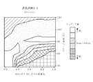
本発明の処理について説明する前に、比較例の処理についてウエハWの表面部の縦断側面図である図1を参照しながら説明する。図1(a)に示すように、ウエハWの表面部は、Si(シリコン)層11、酸化シリコン膜12、ポリシリコン膜13が下方から上方へ向けてこの順に積層されることで構成されている。この処理例では、ウエハWにIF7ガスを供給し、酸化シリコン膜12が露出しないようにシリコン含有膜であるポリシリコン膜13の上部側をエッチングする。ポリシリコン膜13には、例えば酸化シリコンによって構成される不純物14が混入している。
Before explaining the processing of the present invention, the processing of the comparative example will be described with reference to FIG. 1, which is a vertical sectional side view of the surface portion of the wafer W. As shown in FIG. 1A, the surface portion of the wafer W is configured by laminating a Si (silicon)
IF7ガスのシリコン含有膜に対するエッチング選択性は比較的高いため、エッチングレートが比較的高くなる。従って、ポリシリコン膜13は下方へ向けて急激にエッチングされる(図1(b))。そのエッチングの進行中に上記の不純物14が露出するが、IF7ガスの不純物14に対するエッチング選択性は比較的低いため、この不純物14がマスクとして作用する。そのために、ウエハWの面内において不純物14の下方ではエッチングが進行し難く、不純物14が存在しない箇所では引き続き急激なエッチングが行われる。図1(c)はエッチング終了後のウエハWを示している。上記のように不純物14が存在することによって、ウエハWの面内各部のエッチング量について比較的大きなばらつきが生じる。また、このIF7ガスによるエッチングを行うと、残留するポリシリコン膜13の表面の荒れが比較的大きくなってしまうことが確認されている(図1(c))。
Since the etching selectivity of the IF 7 gas for the silicon-containing film is relatively high, the etching rate is relatively high. Therefore, the
続いて本発明の処理の概要と、その処理中に発生すると推定される反応とを図2を参照して説明する。この処理では、塩基性ガスであるNH3(アンモニア)ガスが添加されたIF7ガスをエッチングガスとして、例えば既述の表面部を備えるウエハWに供給する(図2(a))。IF7ガスとNH3ガスとは、下記の式1で示すように互いに反応し、NH4F(フッ化アンモニウム)を生成し、このNH4FがウエハWの表面に付着する付着物となると考えられる。
3IF7+aNH3=3IF5+bHF+cNH4F+N2・・・式1
(ただし、a=2〜5、b=8−a(=0〜6)、c=a−2(=0〜3))
Subsequently, the outline of the process of the present invention and the reaction presumed to occur during the process will be described with reference to FIG. In this treatment, IF 7 gas to which NH 3 (ammonia) gas, which is a basic gas, is added is supplied as an etching gas to, for example, the wafer W provided with the above-mentioned surface portion (FIG. 2 (a)). When the IF 7 gas and the NH 3 gas react with each other as shown in the following formula 1 to form NH 4 F (ammonium fluoride), and this NH 4 F becomes an deposit adhering to the surface of the wafer W. Conceivable.
3IF 7 + aNH3 = 3IF 5 + bHF + cNH 4 F + N 2 ... Equation 1
(However, a = 2-5, b = 8-a (= 0 to 6), c = a-2 (= 0 to 3))
そして、ウエハWの表面に付着したNH4Fは不純物14と反応し、当該不純物14がエッチングされる。またこのNH4FがウエハWに付着した状態でIF7ガスが供給されることになるので、ポリシリコン膜13のエッチングレートが大きくなりすぎることが抑制される。従って、ウエハWの表面に露出した不純物14についてはエッチングにより除去される一方で、不純物14が存在しない領域では急激なポリシリコン膜13のエッチングが防がれるように、エッチングが進行する(図2(b))。なお、ウエハWに付着したNH4Fについては後に詳しく述べるように、このエッチング中のウエハWの加熱温度によっては昇華して除去される。図2(c)はエッチング終了後のウエハWを示している。既述のようにエッチングが進行した結果として、この図2(c)に示すように、ウエハWの面内で均一性高くポリシリコン膜13がエッチングされる。また、このようにエッチングを行うことで、ポリシリコン膜13の表面の荒れが抑制されることが確認されている。
Then, NH 4 F adhering to the surface of the wafer W reacts with the
続いて、上記のIF7ガス及び添加ガスであるNH3ガスを用いてエッチングを行うエッチングモジュール4を含む基板処理装置2について、図2の平面図を参照して説明する。基板処理装置2は、ウエハWを搬入出するための搬入出部21と、搬入出部21に隣接して設けられた2つのロードロック室31と、2つのロードロック室31に各々隣接して設けられた、2つの熱処理モジュール30と、2つの熱処理モジュール30に各々隣接して設けられた2つのエッチングモジュール4と、を備えている。
Subsequently, the
搬入出部21は、第1の基板搬送機構22が設けられると共に常圧雰囲気とされる常圧搬送室23と、当該常圧搬送室23の側部に設けられた、ウエハWを収納するキャリア24が載置されるキャリア用載置台25と、を備えている。図中26は常圧搬送室23に隣接するオリエンタ室であり、ウエハWを回転させて偏心量を光学的に求め、第1の基板搬送機構22に対するウエハWの位置合わせを行うために設けられる。第1の基板搬送機構22は、キャリア用載置台25上のキャリア24とオリエンタ室26とロードロック室31との間でウエハWを搬送する。
The carry-in / out
各ロードロック室31内には、例えば多関節アーム構造を有する第2の基板搬送機構32が設けられており、当該第2の基板搬送機構32は、ウエハWをロードロック室31と熱処理モジュール30とエッチングモジュール4との間で搬送する。熱処理モジュール30を構成する処理容器内及びエッチングモジュール4を構成する処理容器内は真空雰囲気として構成されており、ロードロック室31内は、これらの真空雰囲気の処理容器内と常圧搬送室23との間でウエハWの受け渡しを行えるように、常圧雰囲気と真空雰囲気とが切り替えられる。
In each
図中23は開閉自在なゲートバルブであり、常圧搬送室23とロードロック室31との間、ロードロック室31と熱処理モジュール30との間、熱処理モジュール30とエッチングモジュール4との間に各々設けられている。熱処理モジュール30については、ウエハWを格納すると共に内部が排気されて真空雰囲気とされる処理容器、及び処理容器内に設けられると共に載置されたウエハWを加熱可能な載置台などを含む。そのような構成を備えることで、上記のIF7ガス及びNH3ガスを用いたエッチングを行った後のウエハWに対して加熱処理を行い、エッチングによりウエハWに付着した残渣を除去することができるように構成されている。
In the figure, 23 is a gate valve that can be opened and closed, and is between the normal
続いてエッチングモジュール4について、縦断側面図である図4を参照して説明する。エッチングモジュール4は、処理容器41と、処理容器41の内部に配置された載置台42と、処理容器41の上部にて載置台42と対向するように配置されたガスシャワーヘッド5と、処理容器41の内部を排気して当該処理容器41内の圧力を調整する排気ユニット43とを備える。図中40は処理容器41に形成されたウエハWの搬送口であり、上記のゲートバルブ33により開閉される。既述の載置台42の上面には、ウエハWが水平に載置される。図中44は、載置台42に埋設されたヒーターであり、当該載置台42に載置されたウエハWが設定された温度になるように加熱する。載置台42には、既述の第2の基板搬送機構32との間でウエハWの受け渡しを行うために、その上面を突没自在な3本の昇降ピンが設けられるが、図示は省略している。
Subsequently, the
ガス供給部であるガスシャワーヘッド5は水平な板状体として構成されている。ガスシャワーヘッド5の上側、下側には扁平な拡散空間51、52が各々設けられており、これら拡散空間51、52は互いに区画されている。ガスシャワーヘッド5の下面には、互いに区画されたガス吐出口54、55が各々多数開口しており、ガス吐出口54は拡散空間51に、ガス吐出口55は拡散空間52に夫々接続されている。
The
拡散空間51の上部側にはガス流路56の下流端が接続されている。ガス流路56の上流側は分岐してガス流路57、58を形成し、ガス流路57、58の上流側はIF7ガスの供給源61、Ar(アルゴン)ガス供給源62に夫々接続されている。拡散空間52の上部側には、ガス流路56に対して区画されたガス流路63の下流端が接続されている。ガス流路63の上流側は分岐してガス流路64、65を形成し、ガス流路64、65の上流側はNH3ガスの供給源66、Arガス供給源67に夫々接続されている。ガス流路57、58、64、65にはバルブやマスフローコントローラーにより構成された流量調整部68が各々介設されており、各流路の下流側へのガスの給断、及び各流路の下流側へのガスの流量の調整が行われる。上記のArガスは、処理容器41内のIF7ガス及びNH3ガスを希釈するための希釈ガスである。上記のようにエッチングモジュール4が構成されることで、ガス供給源61、66から供給されたIF7ガス及びNH3ガスはガスシャワーヘッド5から吐出されるまでは、互いに混合されず、ガスシャワーヘッド5から吐出後に処理容器41内で互いに混合される。
The downstream end of the
図3に示すように、基板処理装置2はコンピュータである制御部20を備えており、この制御部20は、プログラム、メモリ、CPUを備えている。プログラムには、既述したウエハWの処理及びウエハWの搬送が行われるように命令(各ステップ)が組み込まれており、このプログラムは、コンピュータ記憶媒体、例えばコンパクトディスク、ハードディスク、光磁気ディスク、DVD等に格納され、制御部20にインストールされる。制御部20は当該プログラムにより基板処理装置2の各部に制御信号を出力し、各部の動作を制御する。具体的には、エッチングモジュール4の動作、熱処理モジュール30の動作、第1の基板搬送機構22、第2の基板搬送機構32の動作、オリエンタ室26の動作が制御信号により制御される。上記のエッチングモジュール4の動作としては、ヒーター44の出力の調整、各流量調整部68による各ガスの流量調整及び各ガスの給断、排気ユニット43による排気流量の調整などの各動作が含まれる。この制御部20及びエッチングモジュール4により、本発明のエッチング装置が構成されている。
As shown in FIG. 3, the
基板処理装置2におけるウエハWの処理を説明する。ここでは、図5に示すウエハWを処理するものとして説明する。このウエハWの表面には酸化シリコン膜12が設けられている。当該酸化シリコン膜12には貫通孔16が形成されており、当該貫通孔16内に埋め込まれるようにポリシリコン膜13が形成されている。この処理例では、当該ポリシリコン膜13の上部側をエッチングする。
The processing of the wafer W in the
図5で説明したウエハWを格納したキャリア24がキャリア用載置台25に載置される。そして、このウエハWは、常圧搬送室23→オリエンタ室26→常圧搬送室23→ロードロック室31の順に搬送され、熱処理モジュール30を介してエッチングモジュール4の処理容器41内に搬送される。そして、当該ウエハWは載置台42に載置されて、例えば80℃に加熱される。その一方で、処理容器41内の圧力、つまりウエハWの周囲の圧力が例えば13.3Pa(100mTorr)〜66.6Pa(500mTorr)とされる。このような比較的小さい圧力とするのは、既述のようにIF7ガスのシリコン含有膜であるポリシリコン膜13のエッチングレートが大きくなりすぎることを抑制することを目的としている。
The
続いて、ガスシャワーヘッド5からIF7ガスとNH3ガスとArガスとが処理容器41内に供給される。図2で説明したようにIF7ガスとNH3ガスとが互いに反応してNH4Fを生じ、当該NH4FがウエハWに付着する。ウエハWは80℃に加熱されており、この温度においてはウエハWに付着したNH4Fガスは昇華する。このようにウエハWの表面でNH4Fの付着と昇華とが行われた状態で、IF7ガスによるポリシリコン膜13のエッチングが進行し、当該エッチングによりウエハWの表面に凹部18が形成され、その深さが次第に大きくなる。
Subsequently, IF 7 gas, NH 3 gas, and Ar gas are supplied from the
図2で述べたシリコン酸化物からなる不純物14がポリシリコン膜13に含まれていても、当該ポリシリコン膜13はウエハWに付着するNH4Fにより除去され、また、当該NH4Fによりポリシリコン膜13のエッチングレートが過剰に大きくなることが抑制される。結果として、図2で述べたポリシリコン膜13をエッチングする場合と同様に、ウエハWの面内で均一性高くポリシリコン膜13がエッチングされる。なお、NH4Fについては不純物14の他に酸化シリコン膜12についても作用すると考えられるが、行われた実験により、酸化シリコン膜12の外形は殆ど変化しない(膜Lossが無い)ことが確認されている。不純物14に関しては膜中に含まれる量が微量であるために、当該NH4Fによって十分に除去されるものと考えられる。
Also
然る後、IF7ガス、NH3ガス及びArガスの供給開始から所定の時間経過後、ガスシャワーヘッド5からこれらの各ガスの供給が停止し、エッチングが終了する。図6は、エッチングが終了した状態のウエハWを示している。上記のようにエッチングが進行したことで凹部18の深さはウエハWの面内で揃っている。また、凹部の底面をなすポリシリコン膜13の荒れが抑制されている。従って、この凹部としては、発明が解決しようとする課題の項目で述べたFootingの発生が抑制されている。エッチングが終了したウエハWは、熱処理モジュール30に搬送されて所定の温度になるように加熱処理を受けて、エッチング残渣が除去された後、ウエハWは、ロードロック室31→常圧搬送室23の順で搬送されて、キャリア24に戻される。
After that, after a predetermined time has elapsed from the start of supply of IF 7 gas, NH 3 gas, and Ar gas, the supply of each of these gases is stopped from the
このエッチングモジュール4を含む基板処理装置2によれば、ウエハWの面内で均一性高くポリシリコン膜13をエッチングし、エッチング後に残るポリシリコン膜13の表面の荒れを抑制することができる。さらに、上記の処理によればプラズマを用いる必要が無いため、ウエハWの表面の各膜が当該プラズマからのダメージを受けることが無いので、ウエハWから形成される半導体装置の信頼性を高くすることができるという利点も有る。ただし、プラズマを用いてエッチングを行う場合も本発明の権利範囲に含まれる。なお、基板処理装置2において図5に示したウエハWを処理するものとして説明したが、図2(a)に示したウエハWを処理するようにしてもよい。従って、基板処理装置2は孔や凹部内に埋め込まれたシリコン含有膜をエッチングすることには限られない。
According to the
また、上記の各処理例についてはポリシリコン膜13の上側のみをエッチングする例を示したが、ウエハW表面に形成されたポリシリコン膜13全体をエッチングするように処理を行ってもよい。その場合は、ウエハWの面内各部におけるポリシリコン膜13のエッチングレートの均一性が高いので、エッチングに要する時間を抑えることができるという効果が得られる。より具体的に述べると、ウエハWの面内でのエッチングレートのばらつきが大きい場合には、ウエハWの面内のうちの一の領域ではエッチングが既に終了していても、他の領域ではエッチングレートが低いことによりエッチングが終了していない状態となるため、面内の全ての領域でポリシリコン膜13がエッチングされるように一の領域がエッチングされた後もエッチングが行われるようにエッチング時間を設定することになる。つまり一の領域についてはオーバーエッチングが行われる時間が設定されることになる。しかしエッチングレートの均一性が高いことにより、そのようなオーバーエッチングの時間を短縮化したり無くしたりすることができるので、上記のようにエッチングに要する時間を抑えることができることになる。
Further, in each of the above treatment examples, an example in which only the upper side of the
ところで、上記のポリシリコン膜13をエッチングする処理例ではIF7ガス及びNH3ガスを同時に処理容器41内に供給している。即ち、IF7ガスを供給する期間と、NH3ガスを供給する期間とが互いに一致するように重なっている。
そのようにIF7ガス及びNH3ガスを供給しなくてもよい。先ず、IF7ガス及びNH3ガスのうち、NH3ガスのみを処理容器41内に供給してウエハWに吸着させる。その後、NH3ガスの供給を停止し、IF7ガス及びNH3ガスのうちIF7ガスのみをウエハWに供給して、ウエハWに吸着したNH3ガスと反応させてNH4Fを発生させて不純物14を除去すると共に、IF7ガスによるポリシリコン膜13のエッチングが行われるようにしてもよい。つまり、NH3ガスとIF7ガスとをこの順番でウエハWに供給して処理を行ってもよい。この順番によるガス供給を繰り返し行ってもよい。即ち、NH3ガス、IF7ガスをこの順番に供給した後に、NH3ガス、IF7ガスを再びこの順番で供給してもよい。このようにNH3ガスはIF7ガスに添加されるようにウエハWに供給されることには限られない。その他にも例えば、IF7ガス及びNH3ガスを同時にウエハWに供給開始した後、IF7ガスの供給が停止されるよりも先にNH3ガスの供給の停止が行われるようにしてもよい。つまり、IF7ガスを供給する期間と、NH3ガスを供給する期間とが重なることは、これらの期間が互いに一致することには限られない。
By the way, in the above-mentioned processing example of etching the
As such it is not necessary to supply the IF 7 gas and NH3 gas. First, of the IF 7 gas and the NH 3 gas, only the NH 3 gas is supplied into the
ところでシリコン含有膜はシリコンを主成分として含む膜であり、ポリシリコン膜には限られない。具体的に、例えばアモルファスシリコン膜、単結晶シリコン膜、SiGe膜、SiC膜などがシリコン含有膜に含まれる。またIF7ガスの他にウエハWに供給される塩基ガスとしては、IF7ガスと反応してNH4Fと同様に窒素及びフッ素を含み、酸化物に対してエッチング作用を有する化合物を生成することができればよいと考えられるので、NH3ガス以外の塩基性ガスを用いるようにしてもよい。具体的に塩基性ガスには、N2H4(ヒドラジン)、アミンである(CH3)NH2(メチルアミン)や、ブチルアミン、ジメチルアミンなどが含まれる。 By the way, the silicon-containing film is a film containing silicon as a main component, and is not limited to a polysilicon film. Specifically, for example, an amorphous silicon film, a single crystal silicon film, a SiGe film, a SiC film and the like are included in the silicon-containing film. In addition to the IF 7 gas, the base gas supplied to the wafer W reacts with the IF 7 gas to produce a compound containing nitrogen and fluorine like NH 4 F and having an etching action on the oxide. since it is considered that it is sufficient, it may be used a basic gas other than NH 3 gas. Specifically, the basic gas includes N 2 H 4 (hydrazine), amine (CH 3 ) NH 2 (methylamine), butylamine, dimethylamine and the like.
上記のエッチングモジュール4において、IF7ガス、NH3ガスが例えばガスシャワーヘッド5内の共通の拡散空間に供給されるように構成されていてもよい。詳しく述べると、ガスシャワーヘッド5内でこれらIF7ガス及びNH3ガスの混合が行われ、この混合ガスがウエハWに吐出されるように、ガスシャワーヘッド5が構成されていてもよい。また、上記のエッチングモジュール4においては、ガスシャワーヘッド5の代わりに、例えば平面視ウエハWの周に沿うように同心円状に開口したガスの吐出口を備えるガス供給部を設けて、ウエハWにガスが供給される構成としてもよい。つまり、ガス供給部としては、ガスシャワーヘッドとして構成されることには限られない。なお、本発明としては既述の実施例や後述の評価試験で述べる例には限られず、各例は適宜変更したり、互いに組み合わせることができる。
In the
(評価試験)
本発明に関連して行われた評価試験について説明する。
評価試験1
評価試験1として、図4で説明したエッチングモジュール4と略同様に構成されたエッチング装置を用いて、図5で説明した構造を有するウエハWにIF7ガス、NH3ガス及びArガスを同時に供給して、ポリシリコン膜13をエッチングした。そして、エッチング後にTEM(透過型電子顕微鏡)を用いて、ウエハWの縦断側面の画像を取得した。IF7ガスの流量は20〜500sccm、NH3ガスの流量は10〜500sccm、Arガスの流量は100〜1000sccmに設定した。これらのガスの供給時間、即ちエッチング時間は3秒、処理容器41内の圧力は6.66〜199.9Pa(50〜1500mTorr)、ウエハWの温度は20〜100℃に夫々設定した。
(Evaluation test)
The evaluation test conducted in connection with the present invention will be described.
Evaluation test 1
As the evaluation test 1, IF 7 gas, NH 3 gas, and Ar gas are simultaneously supplied to the wafer W having the structure described in FIG. 5 by using an etching apparatus configured in substantially the same manner as the
また評価試験1とは異なる処理条件で、図5で説明した構造を有するウエハWにおけるポリシリコン膜13のエッチングを行い、評価試験1と同様にエッチング後のウエハWの縦断側面の画像を取得する比較試験1−1、1−2を行った。比較試験1−1では、F2(フッ素)ガスを200〜1000sccm、NH3ガスを5〜100sccm、N2ガスを50〜1000sccmで夫々同時に処理容器41内に供給してエッチングを行った。これらの各ガスは処理容器41に断続的に7回供給しており、N回目(Nは整数)の供給が行われた後、N+1回目の供給が行われる前に、パージガスによる処理容器41内のパージを行った。また1回のF2ガス、NH3ガス及びN2ガスの供給時間は30秒に設定した。また、処理容器41内の圧力は13.33〜333.3Pa(100〜2500mTorr)、ウエハWの温度は30〜120℃に夫々設定した。比較試験1−2としては、ClF3(三塩化フッ素)ガスを50〜500sccm、N2ガスを100〜1500sccmで処理容器41内に夫々同時に供給してエッチングを行った。これらのガスの処理容器41への供給回数は、評価試験1と同じく1回であり、ガスの供給時間は36.3秒とした。また、処理容器41内の圧力は13.33〜333.3Pa(100〜2500mTorr)、ウエハWの温度は30〜120℃に夫々設定した。
Further, the
評価試験1については、凹部18の底部をなすエッチング後のポリシリコン膜13の表面の平坦性は高く、Footingは見られなかった。従って、ウエハWの面内各部で均一性高くエッチングが行われたことが確認された。そして、凹部18の深さ=エッチング量は50nmであった。なお、既述した図6は、この評価試験1で取得されたTEM画像を概略図として表したものである。また、図7は比較試験1−1から得られたTEM画像を、図8は比較試験1−2から得られたTEM画像を夫々概略図として表したものである。これらの図7、8に示すように、比較試験1−1、1−2では評価試験1に比べてポリシリコン膜13の表面の平坦性は低く、Footingが見られた。また、比較試験1−1ではエッチング量は30nmであり、比較試験1−2ではエッチング量は36.3nmであった。従って、エッチングレートについて、比較試験1−1、1−2よりも評価試験1の方が大きい。このように、評価試験1の結果からは、IF7ガス及びNH3ガスを用いることで、ウエハWの面内で均一性高く、エッチング後のポリシリコン膜13の荒れが抑制されるように当該ポリシリコン膜13のエッチングを行うことができ、且つ高いエッチングレートが得られることが示された。
In the evaluation test 1, the flatness of the surface of the
また、評価試験1ではIF7ガスに対するNH3ガスの流量比(=NH3ガスの流量/IF7ガスの流量)は0.6である。ウエハWの温度は20〜100℃、処理容器41内の圧力は6.66〜199.9Pa(50〜1500mTorr)に設定されている。従って、このような流量比、ウエハWの温度及び処理容器41内の圧力に設定して処理を行うことで、既述のようにウエハWの面内で均一性高くエッチングを行うことができ、且つ高いエッチングレートが得られることが確認された。なお、本発明者は処理容器41内の圧力について26.6Pa以外の値に設定して評価試験1と同様の試験を行っており、処理容器41内の圧力を13.3Pa(100mTorr)〜133.3Pa(1000mTorr)の範囲内に設定した場合に、評価試験1の結果と同様に良好な凹部18の形状が得られることが確認されている。従って、処理容器41内の圧力は、この13.3Pa〜133.3Paに設定することが好ましい。
Further, in the evaluation test 1, the flow rate ratio of NH 3 gas to IF 7 gas (= flow rate of NH 3 gas / flow rate of IF 7 gas) is 0.6. The temperature of the wafer W is set to 20 to 100 ° C., and the pressure in the
評価試験2
評価試験2−1として、ウエハWの表面にアモルファスシリコン膜を膜厚が200nmとなるように成膜し、図4で説明したエッチングモジュール4と略同様に構成されたエッチング装置を用いてIF7ガス及びNH3ガスを共に8秒供給して、当該アモルファスシリコン膜のエッチングを行った。評価試験1と同じく処理容器41内の圧力は50〜1500mTorrとした。エッチング後は、ウエハWに残留しているアモルファスシリコン膜の表面の画像を取得し、当該アモルファスシリコン膜のエッチング量(200nm−残留しているアモルファスシリコン膜の膜厚)と、ウエハWに残留しているアモルファスシリコン膜の表面のラフネスとを測定した。処理条件のうち、NH3ガスの流量及び載置台42表面の温度(=ウエハWの温度)の組み合わせについては処理毎に変更した。NH3ガス/IF7ガスの流量比(=NH3ガスの流量/IF7ガスの流量)としては、0.2、0.4、0.6、1.2または1.8に設定し、ウエハWの温度については、35℃、60℃、80℃、100℃または120℃に設定した。IF7ガスの流量は20〜500sccmに設定した。また、エッチングを行う前におけるアモルファスシリコン膜の表面のラフネスは2.53nmであり、このラフネスの値については小さいほど平坦性が高いことを示す。
As an evaluation test 2-1 an amorphous silicon film was formed on the surface of the wafer W so as to have a film thickness of 200 nm, and an IF 7 was used using an etching apparatus configured in substantially the same manner as the etching module 4 described with reference to FIG. gas and NH 3 gas are both supplied 8 seconds, it was etched the amorphous silicon film. As in the evaluation test 1, the pressure in the
また、評価試験2−2として、ウエハWの表面にアモルファスシリコン膜の代わりにポリシリコン膜を成膜し、このポリシリコン膜に対してエッチングを行ったことを除いて、評価試験2−1と同様の試験を行った。そして、ポリシリコン膜のエッチング量(200nm−残留しているポリシリコン膜の膜厚)と当該ポリシリコン膜の表面のラフネスとを測定した。エッチングを行う前のアモルファスシリコン膜のラフネスは7.46nmである。 Further, as the evaluation test 2-2, the evaluation test 2-1 and the evaluation test 2-1 except that a polysilicon film was formed on the surface of the wafer W instead of the amorphous silicon film and the polysilicon film was etched. A similar test was performed. Then, the etching amount of the polysilicon film (200 nm-the film thickness of the remaining polysilicon film) and the roughness of the surface of the polysilicon film were measured. The roughness of the amorphous silicon film before etching is 7.46 nm.
図9、図10の各グラフは評価試験2−1の結果を示しており、図11、図12の各グラフは評価試験2−2の結果を示している。図9〜図12の各グラフの縦軸は、ウエハWが載置されるステージの温度=ウエハWの温度を示している。また図9〜図12の各グラフの横軸は、NH3ガス/IF7ガスの流量比である。図9、図11のグラフは、エッチング量についての結果を示している。詳しく述べると、グラフ内において等高線を付すことでエッチング量が近似する領域を囲むと共にエッチング量が比較的離れた領域を互いに区画して示している。そして、等高線に囲まれた各領域を互いに区別するために、当該各領域に互いに異なる模様を付して示している。 The graphs of FIGS. 9 and 10 show the results of the evaluation test 2-1 and the graphs of FIGS. 11 and 12 show the results of the evaluation test 2-2. The vertical axis of each graph of FIGS. 9 to 12 shows the temperature of the stage on which the wafer W is placed = the temperature of the wafer W. The horizontal axis of each graph in FIG. 9 to 12 are flow ratio of NH 3 gas / IF 7 gas. The graphs of FIGS. 9 and 11 show the results for the etching amount. More specifically, by adding contour lines in the graph, the regions where the etching amounts are similar are surrounded and the regions where the etching amounts are relatively distant are separated from each other. Then, in order to distinguish each region surrounded by contour lines from each other, each region is shown with a different pattern.
図10、図12のグラフは、ラフネスについての結果を示している。詳しく述べると、グラフ内において等高線を付すことでラフネスの値が近似する領域を囲むと共にラフネスの値が比較的離れた領域を互いに区画して示している。そして、図9、図11のグラフと同様、等高線に囲まれた各領域を互いに区別するために、当該各領域に互いに異なる模様を付して示している。なお、実際には図9〜図12のグラフはコンピュータグラフィクスにより、エッチング量あるいはラフネスについての分布をカラーのグラデーションによって表示したものであるが、図示の便宜上、既述のように示している。 The graphs of FIGS. 10 and 12 show the results for roughness. More specifically, by adding contour lines in the graph, the regions where the roughness values are similar are surrounded and the regions where the roughness values are relatively distant are separated from each other. Then, as in the graphs of FIGS. 9 and 11, in order to distinguish the regions surrounded by the contour lines from each other, the regions are shown with different patterns. Actually, the graphs of FIGS. 9 to 12 show the distribution of the etching amount or roughness by color gradation by computer graphics, but they are shown as described above for convenience of illustration.
エッチング量について、評価試験2−1においては概ね4〜54nmの範囲内の値、評価試験2−2においては概ね4〜44nmの範囲内の値であった。ラフネスについて、評価試験2−1においては概ね2.5〜5.5nmの範囲内の値、評価試験2−2においては概ね4.0〜8.0nmの範囲内の値であった。従って、評価試験2−1、2−2においてエッチング後に残留したアモルファスシリコン膜、ポリシリコン膜の表面のラフネスの値は、エッチング前のラフネスの値に比べて大きく上昇していない。従って、ウエハWの温度を35℃〜120℃にしてIF7ガス及びNH3ガスを供給するときにおいて、ウエハWの面内で均一性高くエッチングすることができるという本発明の効果が得られることが、この評価試験2の結果から確認された。また、ウエハWの温度が35℃の場合ラフネスの値について、評価試験2−1では4.2以下、評価試験2−2では7.2以下と、エッチング前のラフネスの値からの上昇が比較的抑制されている。この35℃よりウエハWの温度が若干低い値であっても、ラフネスの値は大きく変動しないと考えられることから、ウエハWの温度が例えば30℃〜120℃であるときには、上記のエッチングの均一性を高くすることができる効果が得られると推定される。
The etching amount was a value in the range of about 4 to 54 nm in the evaluation test 2-1 and a value in the range of about 4 to 44 nm in the evaluation test 2-2. Regarding the roughness, the value was in the range of about 2.5 to 5.5 nm in the evaluation test 2-1 and the value was in the range of about 4.0 to 8.0 nm in the evaluation test 2-2. Therefore, the roughness values of the surfaces of the amorphous silicon film and the polysilicon film remaining after etching in the evaluation tests 2-1 and 2-2 are not significantly increased as compared with the values of the roughness before etching. Therefore, when the temperature of the wafer W is set to 35 ° C. to 120 ° C. and IF 7 gas and NH 3 gas are supplied, the effect of the present invention that etching can be performed with high uniformity in the plane of the wafer W can be obtained. However, it was confirmed from the result of this
さらに、図9に示されるように、評価試験2−1についてはウエハWの温度が35℃、60℃である場合、NH3ガス/IF7ガスの流量比が比較的大きいと、エッチング量が比較的小さい。しかし、ウエハWの温度が80℃以上である場合にはNH3ガス/IF7ガスの流量比に関わらず、エッチング量が比較的高い値となっており、具体的には30nm以上であった。そして図10に示されるようにラフネスについては、ウエハWの温度及びNH3ガス/IF7ガスの流量比に関わらず比較的低く、具体的には5.6nm以下であった。 Furthermore, as shown in FIG. 9, 35 ° C. temperature of the wafer W is for evaluation test 2-1, the case of 60 ° C., the NH 3 gas / IF 7 flow ratio of the gas is relatively large, the etching amount Relatively small. However, if the temperature of the wafer W is 80 ° C. or more, regardless of the NH 3 gas / IF 7 flow ratio of the gas, has become etching amount and a relatively high value, in particular were 30nm or more .. As shown in FIG. 10, the roughness was relatively low regardless of the temperature of the wafer W and the flow rate ratio of NH 3 gas / IF 7 gas, and was specifically 5.6 nm or less.
また、図11に示されるように、評価試験2−2についてはウエハWの温度が35℃、60℃である場合、NH3ガス/IF7ガスの流量比が比較的大きいと、エッチング量が比較的小さい。しかし、ウエハWの温度が80℃以上である場合にはNH3ガス/IF7ガスの流量比に関わらず、エッチング量が比較的高い値となっており、具体的には29nm以上であった。そして、NH3ガス/IF7ガスの流量比が0.2、0.6、1.2、1.8である場合に、ウエハWの温度を120℃とするよりもウエハWの温度を100℃とした方が、エッチング量が大きい。従って、ウエハWの温度については120℃とするよりも100℃とした方が、エッチング量について大きくなる傾向が有ることが分かる。そして図12から明らかなように、ラフネスについては、ウエハWの温度及びNH3ガス/IF7ガスの流量比に関わらず比較的低く、具体的には9nm以下であった。このような評価試験2−1、2−2の結果から、アモルファスシリコン膜及びポリシリコン膜について、高いエッチングレートを得ると共にエッチング後のラフネスを抑制するためには、エッチング時のウエハWの温度を80℃〜100℃とすることが、より好ましいことが分かる。 Further, as shown in FIG. 11, 35 ° C. temperature of the wafer W is for evaluation test 2-2, the case of 60 ° C., the NH 3 gas / IF 7 flow ratio of the gas is relatively large, the etching amount Relatively small. However, if the temperature of the wafer W is 80 ° C. or more, regardless of the NH 3 gas / IF 7 flow ratio of the gas, has become etching amount and a relatively high value, specifically was more than 29nm .. When the flow rate ratio of NH 3 gas / IF 7 gas is 0.2, 0.6, 1.2, 1.8, the temperature of the wafer W is 100 rather than the temperature of the wafer W being 120 ° C. The etching amount is larger at ° C. Therefore, it can be seen that the etching amount tends to be larger when the temperature of the wafer W is 100 ° C. than when it is 120 ° C. And as evident from FIG. 12, for roughness, relatively low regardless of the flow rate ratio of temperature and NH 3 gas / IF 7 gas of the wafer W, specifically was 9nm or less. From the results of such evaluation tests 2-1 and 2-2, in order to obtain a high etching rate for the amorphous silicon film and the polysilicon film and suppress the roughness after etching, the temperature of the wafer W at the time of etching is adjusted. It can be seen that the temperature is more preferably 80 ° C to 100 ° C.
さらに、評価試験2−1、2−2において、ウエハWの温度が80℃の場合と100℃の場合とを比較すると、NH3ガス/IF7ガスの流量比が同じであるときには、ウエハWの温度が80℃である場合の方が、エッチング量が大きい。また、NH3ガス/IF7ガスの流量比が0.2、0.4であるときには、ウエハWの温度が80℃の場合の方がラフネスの値が小さい。また、評価試験2−2において、ウエハWの温度が80℃の場合と100℃の場合とを比較すると、NH3ガス/IF7ガスの流量比が同じであるときには、ウエハWの温度が80℃である場合の方が、エッチング量が大きく且つラフネスの値が小さい。このように評価試験2で設定されたウエハWの温度の中では80℃が、エッチングレートを高くし、且つエッチング後のラフネスを抑制する観点から最も好ましい値となった。
Further, in the evaluation test 2-1, the temperature of the wafer W is compared with the cases of 80 ° C. and 100 ° C., when the flow rate of NH 3 gas / IF 7 gas are the same, the wafer W The etching amount is larger when the temperature is 80 ° C. Further, when the flow rate ratio of NH 3 gas / IF 7 gas is 0.2 or 0.4, the roughness value is smaller when the temperature of the wafer W is 80 ° C. Further, in the evaluation test 2-2, the temperature of the wafer W is compared with the cases of 80 ° C. and 100 ° C., when the flow rate of NH 3 gas / IF 7 gas are the same, the temperature of the wafer W is 80 At ° C, the etching amount is large and the roughness value is small. Among the temperatures of the wafer W set in the
ところでエッチング時の処理容器41内の圧力を上記のように設定しているため、ウエハWの温度が80℃以上であるときに、NH4FはウエハWから昇華する。評価試験2−1、2−2でウエハWの温度が80℃以上である場合にエッチング量が比較的大きいのは、NH4Fが付着してもそのように昇華が起きるため、IF7ガスのエッチング作用が当該NH4Fにより大きく妨げられないためであると考えられる。ただし、NH3ガス及びNH4FがウエハWに吸着する確率は、ウエハWの温度が低いほど高くなる。従って、エッチング時にウエハWの温度が高すぎると、当該NH4Fの作用が弱くなる。そのような理由により、ウエハWの温度が120℃である場合よりも100℃である場合の方が好ましく、ウエハWの温度が80℃である場合の方がより好ましい結果になったと推定される。そして、この80℃から若干変動した温度であってもエッチングレートが高く且つラフネスが低くなると考えられる。上記のようにウエハWの温度が80℃以上であるときにNH4Fを昇華させることができることを考えると、特に好ましいウエハWの温度範囲はその80℃以上の温度であり100℃より低い温度、具体的には80℃〜90℃であると考えられる。
By the way, since the pressure in the
ところで評価試験2−1においてウエハWの温度が35℃または60℃である場合の結果を見ると、NH3ガスの流量がIF7ガスの流量よりも大きいとき、つまりNH3ガス/IF7ガスの流量比が1.2、1.8であるときには、エッチング量は比較的小さい。しかし、NH3ガスの流量がIF7ガスの流量よりも小さいとき、つまりNH3ガス/IF7ガスの流量比が0.2〜0.6であるとき、ウエハWの温度が35℃且つNH3ガス/IF7ガスの流量比が0.6である場合の結果を除いてエッチング量が比較的大きい結果となっている。 By the way, looking at the results when the temperature of the wafer W is 35 ° C or 60 ° C in the evaluation test 2-1 when the flow rate of NH 3 gas is larger than the flow rate of IF 7 gas, that is, NH 3 gas / IF 7 gas. When the flow rate ratio of is 1.2 and 1.8, the etching amount is relatively small. However, when the flow rate of the NH 3 gas is less than the flow rate of the IF 7 gas, that is, when the flow ratio of NH 3 gas / IF 7 gas is 0.2 to 0.6, the temperature of the wafer W and 35 ° C. NH Except for the case where the flow rate ratio of 3 gas / IF 7 gas is 0.6, the result is that the etching amount is relatively large.
また評価試験2−2においてウエハWの温度が35℃または60℃である場合の結果を見ると、NH3ガス/IF7ガスの流量比が1.2、1.8であるときには、エッチング量が比較的小さい。そして、NH3ガス/IF7ガスの流量比が0.2〜0.6であるとき、ウエハWの温度が35℃且つNH3ガス/IF7ガスの流量比が0.6である場合を除いてエッチング量が比較的大きい結果となっている。 Further to the results when the temperature of the wafer W is 35 ° C. or 60 ° C. In evaluation tests 2-2, when the flow rate of NH 3 gas / IF 7 gas is 1.2,1.8, the etching amount Is relatively small. When the flow rate ratio of NH 3 gas / IF 7 gas is 0.2 to 0.6, the temperature of the wafer W is 35 ° C. and the flow rate ratio of NH 3 gas / IF 7 gas is 0.6. Except for this, the etching amount is relatively large.
このような結果となったのは、上記のようにNH4FがウエハWから昇華する温度は80℃以上であり、この昇華が起こらない35℃、60℃の場合はNH3ガスの流量が比較的大きいとNH4FのウエハWへの付着量が過剰となることで、IF7ガスによるエッチング量が低下したためであると考えられる。従って、この評価試験2の結果からは、ウエハWの温度が80℃より低い場合、NH3ガス/IF7ガスの流量比を0.6以下とすることが好ましいことが確認された。
The reason for this result is that the temperature at which NH 4 F sublimates from the wafer W is 80 ° C or higher as described above, and when this sublimation does not occur at 35 ° C and 60 ° C, the flow rate of NH 3 gas is high. relatively
また、評価試験2−1、2−2において、ウエハWの温度を80℃以上に設定した場合、NH3ガス/IF7ガスの流量比によってラフネスの値は大きく変化していないが、エッチング量については、NH3ガス/IF7ガスの流量比を0.6に設定するよりも、1.2または1.8とした方が大きい。従って、ウエハWの温度が80℃以上である場合においては、NH3ガス/IF7ガスの流量比については1.2〜1.8であると、高いエッチングレートを得ると共にエッチング後のラフネスを大きく抑制することができることが確認された。つまり、NH3ガスの流量/IF7ガスの流量については、1.2〜1.8の範囲内とすることが好ましいことが確認された。 Further, in the evaluation test 2-1 and 2-2, when the temperature of the wafer W to 80 ° C. or higher, the value of the roughness does not change greatly depending on the flow rate of NH 3 gas / IF 7 gas, the etching amount for, rather than setting the NH 3 gas / IF 7 gas flow rate of 0.6, is greater that 1.2 or 1.8. Therefore, when the temperature of the wafer W is 80 ° C. or more, as for the NH 3 gas / IF 7 gas flow rate ratio of is 1.2 to 1.8, the roughness after etching with obtaining a high etching rate It was confirmed that it can be greatly suppressed. That is, it was confirmed that the flow rate of NH 3 gas / the flow rate of IF 7 gas is preferably in the range of 1.2 to 1.8.
ところで、ウエハWの温度が80℃以上である場合、NH3ガス/IF7ガスの流量比が1.2よりも若干小さい値であってもエッチング作用は大きく変動しないと考えられ、ウエハWの温度が80℃より低い場合NH3ガス/IF7ガスの流量比が0.6より若干大きい値であってもエッチング作用は大きく変動しないと考えられる。具体的にウエハWの温度が80℃以上である場合、NH3ガス/IF7ガスの流量比については例えば1以上、ウエハWの温度が80℃より低い場合、NH3ガス/IF7ガスの流量比については例えば1以下であれば、エッチング作用の変動は少ないと考えられる。従ってウエハWの温度が80℃以上である場合、NH3ガス/IF7ガスの流量比については、1〜1.8とすることが好ましく、80℃より低い場合、NH3ガスの流量/IF7ガスの流量については、1以下とすることが好ましいと推定される。 Incidentally, when the temperature of the wafer W is 80 ° C. or more, NH 3 gas / IF 7 flow ratio of the gas is considered not to vary significantly etching action be slightly smaller than 1.2, the wafer W temperature is considered to flow rate ratio of lower than 80 ° C. NH 3 gas / IF 7 gas does not vary significantly etching action be slightly larger than 0.6. Specifically, when the temperature of the wafer W is 80 ° C. or higher, the flow rate ratio of NH 3 gas / IF 7 gas is, for example, 1 or more, and when the temperature of the wafer W is lower than 80 ° C., the flow rate of NH 3 gas / IF 7 gas is If the flow rate ratio is, for example, 1 or less, it is considered that the fluctuation of the etching action is small. Therefore, when the temperature of the wafer W is 80 ° C. or higher, the flow rate ratio of NH 3 gas / IF 7 gas is preferably 1 to 1.8, and when the temperature is lower than 80 ° C., the flow rate of NH 3 gas / IF It is estimated that the flow rate of the 7 gases is preferably 1 or less.
W ウエハ
14 ポリシリコン膜
2 基板処理装置
20 制御部
4 エッチングモジュール
42 載置台
5 シャワーヘッド
Claims (8)
前記基板に七フッ化ヨウ素ガスが供給される期間と、前記基板に前記塩基性ガスが供給される期間とは、互いに重なり、
前記基板の温度を80℃以上にした状態で、
当該基板を格納する処理容器内に、前記塩基性ガスの流量/前記七フッ化ヨウ素ガスの流量が1〜1.8となるように、当該塩基性ガス及び七フッ化ヨウ素ガスを供給する工程を含むことを特徴とするエッチング方法。 A substrate having a silicon-containing film is formed on the surface, to supply and a basic gas iodine heptafluoride gas, saw including a step of etching the silicon-containing film,
The period during which the iodine heptafluoride gas is supplied to the substrate and the period during which the basic gas is supplied to the substrate overlap with each other.
With the temperature of the substrate set to 80 ° C or higher,
A step of supplying the basic gas and the iodine heptafluoride gas into the processing container for storing the substrate so that the flow rate of the basic gas / the flow rate of the iodine heptafluoride gas is 1 to 1.8. An etching method comprising.
前記基板に七フッ化ヨウ素ガスが供給される期間と、前記基板に前記塩基性ガスが供給される期間とは、互いに重なり、
前記基板の温度が80℃より低い状態で
当該基板を格納する処理容器内に、前記塩基性ガスの流量/前記七フッ化ヨウ素ガスの流量が1以下となるように、当該塩基性ガス及び七フッ化ヨウ素ガスを供給する工程を含むことを特徴とするエッチング方法。 A substrate having a silicon-containing film is formed on the surface, to supply and a basic gas iodine heptafluoride gas, saw including a step of etching the silicon-containing film,
The period during which the iodine heptafluoride gas is supplied to the substrate and the period during which the basic gas is supplied to the substrate overlap with each other.
When the temperature of the substrate is lower than 80 ° C.
A step of supplying the basic gas and the iodine heptafluoride gas so that the flow rate of the basic gas / the flow rate of the iodine heptafluoride gas is 1 or less is included in the processing container for storing the substrate. An etching method characterized by.
前記基板の温度を120℃以下にした状態で、当該基板に前記七フッ化ヨウ素ガスと前記塩基性ガスとを供給する工程を含むことを特徴とする請求項1記載のエッチング方法。 The step of etching the silicon-containing film is
Wherein the temperature of the substrate while the 120 ° C. or less, etching method of claim 1, characterized in that it comprises a step of supplying the to the substrate with iodine heptafluoride gas and the basic gas.
前記基板の温度を30℃以上にした状態で、当該基板に前記七フッ化ヨウ素ガスと前記塩基性ガスとを供給する工程を含むことを特徴とする請求項2記載のエッチング方法。 The step of etching the silicon-containing film is
The etching method according to claim 2 , further comprising a step of supplying the iodine heptafluoride gas and the basic gas to the substrate in a state where the temperature of the substrate is 30 ° C. or higher.
前記基板を格納する処理容器内の圧力を13.3Pa〜133.3Paにして前記七フッ化ヨウ素ガスと前記塩基性ガスとを供給する工程を含むことを特徴とする請求項1ないし4のいずれか一つに記載のエッチング方法。 The step of etching the silicon-containing film is
Any of claims 1 to 4 , wherein the pressure in the processing container for storing the substrate is set to 13.3 Pa to 133.3 Pa, and the step of supplying the iodine heptafluoride gas and the basic gas is included. The etching method described in one.
前記処理容器内に設けられ、表面にシリコン含有膜が形成された基板を載置すると共に加熱する載置部と、
前記処理容器内に七フッ化ヨウ素ガスと塩基性ガスとを供給して、前記シリコン含有膜をエッチングするガス供給部と、を備え、
前記基板に七フッ化ヨウ素ガスが供給される期間と、前記基板に前記塩基性ガスが供給される期間とは、互いに重なり、
前記載置部により前記基板の温度が80℃以上になるように当該基板を加熱した状態で、
前記ガス供給部は、当該基板を格納する処理容器内に、前記塩基性ガスの流量/前記七フッ化ヨウ素ガスの流量が1〜1.8となるように、当該塩基性ガス及び七フッ化ヨウ素ガスを供給することを特徴とするエッチング装置。 With the processing container
A mounting portion provided in the processing container and having a silicon-containing film formed on the surface thereof is mounted and heated.
The processing container is provided with a gas supply unit for supplying iodine heptafluoride gas and basic gas to etch the silicon-containing film .
The period during which the iodine heptafluoride gas is supplied to the substrate and the period during which the basic gas is supplied to the substrate overlap with each other.
In a state where the substrate is heated so that the temperature of the substrate becomes 80 ° C. or higher by the above-mentioned mounting portion.
The gas supply unit has the basic gas and iodine hepta fluoride so that the flow rate of the basic gas / the flow rate of the iodine heptafluoride gas is 1 to 1.8 in the processing container for storing the substrate. An etching device characterized by supplying iodine gas.
前記処理容器内に設けられ、表面にシリコン含有膜が形成された基板を載置すると共に加熱する載置部と、
前記処理容器内に七フッ化ヨウ素ガスと塩基性ガスとを供給して、前記シリコン含有膜をエッチングするガス供給部と、を備え、
前記基板に七フッ化ヨウ素ガスが供給される期間と、前記基板に前記塩基性ガスが供給される期間とは、互いに重なり、
前記載置部により前記基板の温度が80℃より低くなるように当該基板を加熱した状態で、
前記ガス供給部は、当該基板を格納する処理容器内に、前記塩基性ガスの流量/前記七フッ化ヨウ素ガスの流量が1以下となるように、当該塩基性ガス及び七フッ化ヨウ素ガスを供給することを特徴とするエッチング装置。 With the processing container
A mounting portion provided in the processing container and having a silicon-containing film formed on the surface thereof is mounted and heated.
The processing container is provided with a gas supply unit for supplying iodine heptafluoride gas and basic gas to etch the silicon-containing film .
The period during which the iodine heptafluoride gas is supplied to the substrate and the period during which the basic gas is supplied to the substrate overlap with each other.
In a state where the substrate is heated so that the temperature of the substrate is lower than 80 ° C. by the above-mentioned mounting portion.
The gas supply unit puts the basic gas and the iodine heptafluoride gas in the processing container for storing the substrate so that the flow rate of the basic gas / the flow rate of the iodine heptafluoride gas is 1 or less. An etching device characterized by supplying.
Priority Applications (5)
| Application Number | Priority Date | Filing Date | Title |
|---|---|---|---|
| JP2018005792A JP6981267B2 (en) | 2018-01-17 | 2018-01-17 | Etching method and etching equipment |
| KR1020190002798A KR102229993B1 (en) | 2018-01-17 | 2019-01-09 | Etching method and etching apparatus |
| US16/244,511 US20190221440A1 (en) | 2018-01-17 | 2019-01-10 | Etching Method and Etching Apparatus |
| TW108101455A TWI796416B (en) | 2018-01-17 | 2019-01-15 | Etching method and etching device |
| CN201910043237.0A CN110047747B (en) | 2018-01-17 | 2019-01-17 | Etching method and etching apparatus |
Applications Claiming Priority (1)
| Application Number | Priority Date | Filing Date | Title |
|---|---|---|---|
| JP2018005792A JP6981267B2 (en) | 2018-01-17 | 2018-01-17 | Etching method and etching equipment |
Publications (3)
| Publication Number | Publication Date |
|---|---|
| JP2019125715A JP2019125715A (en) | 2019-07-25 |
| JP2019125715A5 JP2019125715A5 (en) | 2020-11-05 |
| JP6981267B2 true JP6981267B2 (en) | 2021-12-15 |
Family
ID=67214216
Family Applications (1)
| Application Number | Title | Priority Date | Filing Date |
|---|---|---|---|
| JP2018005792A Active JP6981267B2 (en) | 2018-01-17 | 2018-01-17 | Etching method and etching equipment |
Country Status (5)
| Country | Link |
|---|---|
| US (1) | US20190221440A1 (en) |
| JP (1) | JP6981267B2 (en) |
| KR (1) | KR102229993B1 (en) |
| CN (1) | CN110047747B (en) |
| TW (1) | TWI796416B (en) |
Families Citing this family (3)
| Publication number | Priority date | Publication date | Assignee | Title |
|---|---|---|---|---|
| JP7345334B2 (en) * | 2019-09-18 | 2023-09-15 | 東京エレクトロン株式会社 | Etching method and substrate processing system |
| JP7550534B2 (en) | 2020-05-15 | 2024-09-13 | 東京エレクトロン株式会社 | Etching method and etching apparatus |
| TW202310038A (en) * | 2021-05-31 | 2023-03-01 | 日商東京威力科創股份有限公司 | Substrate processing method and substrate processing apparatus |
Family Cites Families (15)
| Publication number | Priority date | Publication date | Assignee | Title |
|---|---|---|---|---|
| DE2548615C2 (en) | 1975-10-30 | 1982-06-03 | M.A.N. Maschinenfabrik Augsburg-Nürnberg AG, 8900 Augsburg | Device for controlling a starter and brake valve on a reversible internal combustion engine that can be actuated by fluid pressure, in particular pneumatic pressure |
| US5698070A (en) * | 1991-12-13 | 1997-12-16 | Tokyo Electron Limited | Method of etching film formed on semiconductor wafer |
| US5888906A (en) * | 1996-09-16 | 1999-03-30 | Micron Technology, Inc. | Plasmaless dry contact cleaning method using interhalogen compounds |
| JP2008177209A (en) * | 2007-01-16 | 2008-07-31 | Taiyo Nippon Sanso Corp | Plasma etching method |
| DE102008037943B4 (en) * | 2008-08-14 | 2018-04-26 | Nawotec Gmbh | Method and apparatus for electron-beam-induced etching and semiconductor device etched with a structure by means of such a method |
| JP4968861B2 (en) * | 2009-03-19 | 2012-07-04 | 東京エレクトロン株式会社 | Substrate etching method and system |
| JP5655296B2 (en) * | 2009-12-01 | 2015-01-21 | セントラル硝子株式会社 | Etching gas |
| JP6032033B2 (en) * | 2013-02-01 | 2016-11-24 | セントラル硝子株式会社 | Silicon dry etching method |
| EP3892728A1 (en) | 2013-02-06 | 2021-10-13 | Evolva SA | Methods for improved production of rebaudioside d and rebaudioside m |
| JP6107198B2 (en) * | 2013-02-14 | 2017-04-05 | セントラル硝子株式会社 | Cleaning gas and cleaning method |
| JPWO2015016149A1 (en) * | 2013-07-29 | 2017-03-02 | 株式会社日立国際電気 | Substrate processing apparatus, semiconductor device manufacturing method, and program |
| JP6201496B2 (en) * | 2013-08-02 | 2017-09-27 | セントラル硝子株式会社 | IF7-derived iodine fluoride compound recovery method and recovery device |
| KR20150060069A (en) | 2013-11-25 | 2015-06-03 | 에스티엑스조선해양 주식회사 | Fixing bracket for prefabricated scaffolding |
| JP6210039B2 (en) * | 2014-09-24 | 2017-10-11 | セントラル硝子株式会社 | Deposit removal method and dry etching method |
| JP6544215B2 (en) * | 2015-01-23 | 2019-07-17 | セントラル硝子株式会社 | Dry etching method |
-
2018
- 2018-01-17 JP JP2018005792A patent/JP6981267B2/en active Active
-
2019
- 2019-01-09 KR KR1020190002798A patent/KR102229993B1/en active IP Right Grant
- 2019-01-10 US US16/244,511 patent/US20190221440A1/en not_active Abandoned
- 2019-01-15 TW TW108101455A patent/TWI796416B/en active
- 2019-01-17 CN CN201910043237.0A patent/CN110047747B/en active Active
Also Published As
| Publication number | Publication date |
|---|---|
| US20190221440A1 (en) | 2019-07-18 |
| CN110047747A (en) | 2019-07-23 |
| CN110047747B (en) | 2023-05-23 |
| TWI796416B (en) | 2023-03-21 |
| KR102229993B1 (en) | 2021-03-18 |
| KR20190088009A (en) | 2019-07-25 |
| JP2019125715A (en) | 2019-07-25 |
| TW201936994A (en) | 2019-09-16 |
Similar Documents
| Publication | Publication Date | Title |
|---|---|---|
| JP6568769B2 (en) | Substrate processing method and substrate processing apparatus | |
| JP6981267B2 (en) | Etching method and etching equipment | |
| TWI710015B (en) | Substrate processing method | |
| TWI727023B (en) | Substrate processing method and substrate processing device | |
| JP5809144B2 (en) | Substrate processing method and substrate processing apparatus | |
| WO2018180670A1 (en) | Substrate processing method and storage medium | |
| KR102272823B1 (en) | Etching method and etching apparatus | |
| JP5881612B2 (en) | Semiconductor device manufacturing method and manufacturing apparatus | |
| TWI702647B (en) | Substrate processing method | |
| JP6161972B2 (en) | Etching method and recording medium | |
| TWI791741B (en) | etching method | |
| KR102471284B1 (en) | Etching method and apparatus | |
| JP2022020428A (en) | Etching method and etching equipment | |
| TW202201512A (en) | Etching method and etching device | |
| WO2022102421A1 (en) | Etching method and etching apparatus | |
| US12054824B2 (en) | Substrate processing method and substrate processing apparatus | |
| TWI850239B (en) | Etching method and etching device | |
| WO2024062994A1 (en) | Substrate processing method and substrate processing apparatus | |
| TW202201514A (en) | Etching method and etching device | |
| TW202113966A (en) | Etching method and apparatus |
Legal Events
| Date | Code | Title | Description |
|---|---|---|---|
| A521 | Request for written amendment filed |
Free format text: JAPANESE INTERMEDIATE CODE: A523 Effective date: 20200805 |
|
| A621 | Written request for application examination |
Free format text: JAPANESE INTERMEDIATE CODE: A621 Effective date: 20200805 |
|
| A521 | Request for written amendment filed |
Free format text: JAPANESE INTERMEDIATE CODE: A523 Effective date: 20200915 |
|
| RD02 | Notification of acceptance of power of attorney |
Free format text: JAPANESE INTERMEDIATE CODE: A7422 Effective date: 20200915 |
|
| A977 | Report on retrieval |
Free format text: JAPANESE INTERMEDIATE CODE: A971007 Effective date: 20210617 |
|
| A131 | Notification of reasons for refusal |
Free format text: JAPANESE INTERMEDIATE CODE: A131 Effective date: 20210622 |
|
| A521 | Request for written amendment filed |
Free format text: JAPANESE INTERMEDIATE CODE: A523 Effective date: 20210823 |
|
| TRDD | Decision of grant or rejection written | ||
| A01 | Written decision to grant a patent or to grant a registration (utility model) |
Free format text: JAPANESE INTERMEDIATE CODE: A01 Effective date: 20211019 |
|
| A61 | First payment of annual fees (during grant procedure) |
Free format text: JAPANESE INTERMEDIATE CODE: A61 Effective date: 20211101 |
|
| R150 | Certificate of patent or registration of utility model |
Ref document number: 6981267 Country of ref document: JP Free format text: JAPANESE INTERMEDIATE CODE: R150 |