JP6981004B2 - Optical phase distortion compensation device and optical phase distortion compensation method - Google Patents
Optical phase distortion compensation device and optical phase distortion compensation method Download PDFInfo
- Publication number
- JP6981004B2 JP6981004B2 JP2017000282A JP2017000282A JP6981004B2 JP 6981004 B2 JP6981004 B2 JP 6981004B2 JP 2017000282 A JP2017000282 A JP 2017000282A JP 2017000282 A JP2017000282 A JP 2017000282A JP 6981004 B2 JP6981004 B2 JP 6981004B2
- Authority
- JP
- Japan
- Prior art keywords
- optical
- signal
- phase distortion
- output
- compensation
- Prior art date
- Legal status (The legal status is an assumption and is not a legal conclusion. Google has not performed a legal analysis and makes no representation as to the accuracy of the status listed.)
- Active
Links
- 230000003287 optical effect Effects 0.000 title claims description 334
- 238000000034 method Methods 0.000 title claims description 18
- 230000005540 biological transmission Effects 0.000 claims description 88
- 230000010287 polarization Effects 0.000 claims description 48
- 238000004891 communication Methods 0.000 claims description 18
- 239000000284 extract Substances 0.000 claims description 10
- 238000001514 detection method Methods 0.000 claims description 9
- 238000000926 separation method Methods 0.000 claims description 7
- 238000000605 extraction Methods 0.000 claims description 6
- 230000002123 temporal effect Effects 0.000 claims description 6
- 230000001934 delay Effects 0.000 claims description 3
- 239000013307 optical fiber Substances 0.000 description 32
- 238000010586 diagram Methods 0.000 description 24
- 101100381996 Saccharomyces cerevisiae (strain ATCC 204508 / S288c) BRO1 gene Proteins 0.000 description 10
- 230000002441 reversible effect Effects 0.000 description 7
- 230000006870 function Effects 0.000 description 6
- 238000003780 insertion Methods 0.000 description 6
- 230000037431 insertion Effects 0.000 description 6
- 230000004044 response Effects 0.000 description 5
- 230000000694 effects Effects 0.000 description 4
- 239000006185 dispersion Substances 0.000 description 3
- 239000000203 mixture Substances 0.000 description 2
- 238000012544 monitoring process Methods 0.000 description 2
- 229910013641 LiNbO 3 Inorganic materials 0.000 description 1
- 230000003111 delayed effect Effects 0.000 description 1
- 238000001914 filtration Methods 0.000 description 1
- GQYHUHYESMUTHG-UHFFFAOYSA-N lithium niobate Chemical compound [Li+].[O-][Nb](=O)=O GQYHUHYESMUTHG-UHFFFAOYSA-N 0.000 description 1
- 230000000243 photosynthetic effect Effects 0.000 description 1
- 238000012545 processing Methods 0.000 description 1
- 230000000644 propagated effect Effects 0.000 description 1
Images


Classifications
-
- H—ELECTRICITY
- H04—ELECTRIC COMMUNICATION TECHNIQUE
- H04B—TRANSMISSION
- H04B10/00—Transmission systems employing electromagnetic waves other than radio-waves, e.g. infrared, visible or ultraviolet light, or employing corpuscular radiation, e.g. quantum communication
- H04B10/50—Transmitters
- H04B10/516—Details of coding or modulation
- H04B10/548—Phase or frequency modulation
- H04B10/556—Digital modulation, e.g. differential phase shift keying [DPSK] or frequency shift keying [FSK]
- H04B10/5561—Digital phase modulation
-
- H—ELECTRICITY
- H04—ELECTRIC COMMUNICATION TECHNIQUE
- H04B—TRANSMISSION
- H04B10/00—Transmission systems employing electromagnetic waves other than radio-waves, e.g. infrared, visible or ultraviolet light, or employing corpuscular radiation, e.g. quantum communication
- H04B10/25—Arrangements specific to fibre transmission
- H04B10/2507—Arrangements specific to fibre transmission for the reduction or elimination of distortion or dispersion
- H04B10/2543—Arrangements specific to fibre transmission for the reduction or elimination of distortion or dispersion due to fibre non-linearities, e.g. Kerr effect
- H04B10/2557—Cross-phase modulation [XPM]
-
- H—ELECTRICITY
- H04—ELECTRIC COMMUNICATION TECHNIQUE
- H04J—MULTIPLEX COMMUNICATION
- H04J14/00—Optical multiplex systems
- H04J14/02—Wavelength-division multiplex systems
- H04J14/03—WDM arrangements
- H04J14/0307—Multiplexers; Demultiplexers
Landscapes
- Engineering & Computer Science (AREA)
- Computer Networks & Wireless Communication (AREA)
- Signal Processing (AREA)
- Physics & Mathematics (AREA)
- Electromagnetism (AREA)
- Nonlinear Science (AREA)
- Optical Communication System (AREA)
- Optical Modulation, Optical Deflection, Nonlinear Optics, Optical Demodulation, Optical Logic Elements (AREA)
Description
本発明は、伝送路中で生じる光位相歪を補償する光位相歪補償装置および光位相歪補償方法に関する。 The present invention relates to an optical phase distortion compensating device and an optical phase distortion compensating method for compensating for optical phase distortion occurring in a transmission line.
伝送路は、波長分割多重(WDM:Wavelength Division Multiplex)通信により、入力する光信号数の増加、および波長間隔の狭窄化で伝送容量を拡大できる。これら光信号数の増加や波長間隔の狭窄化に伴い、伝送路中で生じる相互位相変調による光位相歪が増大し、伝送容量の増大と伝送距離の延長を両立することが困難となる。伝送路中で生じる光位相歪を補償できることで、伝送容量を増大させた光信号を長距離伝送できるようになる。 The transmission line can expand the transmission capacity by increasing the number of optical signals to be input and narrowing the wavelength interval by wavelength division multiplexing (WDM) communication. As the number of optical signals increases and the wavelength interval becomes narrower, the optical phase distortion due to mutual phase modulation that occurs in the transmission line increases, and it becomes difficult to achieve both an increase in transmission capacity and an extension in transmission distance. By being able to compensate for the optical phase distortion that occurs in the transmission line, it becomes possible to transmit an optical signal with an increased transmission capacity over a long distance.
図12は、伝送路で生じる光位相歪を説明する図である。図12(a)は波長多重された光信号(WDM信号)の時間−光強度特性の例であり、WDM信号の強度変動(数GHz)、変調成分は数十GHzである。図12(b)に示すWDM信号(波長−光強度特性)を伝送路Dに入力させると、図12(c)のように(b)同様のWDM信号が出力される。ここで、WDM信号の持つ低速な強度変動(数GHz)が伝送路D中で光位相歪を生じ、伝送路Dから出力された(受信側の)WDM信号は、図12(d)の時間−光位相歪特性に示すように、時間経過で変動する光位相歪の成分を有する。 FIG. 12 is a diagram illustrating optical phase distortion that occurs in a transmission line. FIG. 12A is an example of the time-light intensity characteristic of the wavelength-multiplexed optical signal (WDM signal), the intensity variation of the WDM signal (several GHz), and the modulation component is several tens of GHz. When the WDM signal (wavelength-light intensity characteristic) shown in FIG. 12 (b) is input to the transmission line D, the same WDM signal as in (b) is output as shown in FIG. 12 (c). Here, the low-speed intensity fluctuation (several GHz) of the WDM signal causes optical phase distortion in the transmission line D, and the WDM signal output from the transmission line D (on the receiving side) is the time shown in FIG. 12 (d). -As shown in the optical phase distortion characteristics, it has a component of optical phase distortion that fluctuates over time.
従来、伝送路で劣化した光信号を2分岐し、一方をLN(LiNbO3:ニオブ酸リチウム)型位相変調器に入力し、他方の受光器の出力によりLN型位相変調器を制御して光位相歪を補償する技術がある(例えば、下記特許文献1,2参照。)。光位相歪は、例えば、光信号の送信端、受信端、中継箇所で補償できる。送信端では送信装置の後段に、受信端では受信装置の前段に補償器を設け、中継箇所では中継器の光増幅器の後段に補償器を設けている。
Conventionally, an optical signal deteriorated in a transmission line is branched into two, one is input to an LN (LiNbO 3 : lithium niobate) type phase modulator, and the output of the other receiver controls the LN type phase modulator for optical light. There is a technique for compensating for phase distortion (see, for example,
従来技術では、広帯域な伝送帯域(例えば、Cバンド)で発生する光位相歪を補償することができなかった。従来は、上述した波長多重した光信号の比較的低速な強度変動に対応して、光信号を位相変調することで相互位相変調による光位相歪を補償している。この場合、下記の問題がある。
1.既存の位相変調器は挿入損失が大きく偏光依存性が大きい。
2.伝送路中で分布的に発生する光位相歪を位相変調器により補償すると、補償量が小さくなる。
In the prior art, it was not possible to compensate for the optical phase distortion that occurs in a wide band transmission band (for example, C band). Conventionally, the optical phase distortion due to mutual phase modulation is compensated by phase-modulating the optical signal in response to the relatively low-speed intensity fluctuation of the above-mentioned wavelength-multiplexed optical signal. In this case, there are the following problems.
1. 1. The existing phase modulator has a large insertion loss and a large polarization dependence.
2. 2. When the optical phase distortion generated distributed in the transmission line is compensated by the phase modulator, the compensation amount becomes small.
位相変調器による光位相歪の補償では、位相変調器を設けることによる付加的な挿入損失が発生する。また、集中定数的に補償するため、分布的に変動しながら発生する位相歪に対し部分的な補償となる。また、変調度の調整は、位相変調器による変調後の位相をモニタする必要があり、複雑な構成となる。 Compensation for optical phase distortion by a phase modulator causes additional insertion loss due to the provision of the phase modulator. In addition, since the compensation is performed in a lumped constant, the phase distortion that occurs while fluctuating in a distributed manner is partially compensated. Further, the adjustment of the degree of modulation requires monitoring the phase after modulation by the phase modulator, which is a complicated configuration.
一つの側面では、本発明は、広帯域な伝送帯域で発生する光位相歪を簡単な構成で低損失に補償できることを目的とする。 In one aspect, it is an object of the present invention to be able to compensate for optical phase distortion generated in a wide band transmission band with a simple configuration and low loss.
一つの案では、光位相歪補償装置は、入力される波長多重された光信号の光位相歪を補償する光位相歪補償装置において、前記光信号の強度変動を検出する検出部と、前記強度変動の成分から光位相歪が主に発生する帯域を抽出するフィルタと、前記フィルタの抽出に基づき、入力される光信号の時間的な強度変動を有する補償信号を生成する制御部と、前記制御部の補償信号に基づき、前記強度変動に対して逆相の強度変動を有し、前記光信号の波長と異なる波長の補償信号光を出力する補償信号光源と、前記光信号と前記補償信号光とを合波した信号光を伝送路へ出力する光合波器と、前記光合波器の出力に接続された非線形媒質と、を有し、前記非線形媒質で光位相変調を生じさせることを要件とする。
In one proposal, the optical phase distortion compensator is an optical phase distortion compensator that compensates for the optical phase distortion of an input wavelength-multiplexed optical signal, and has a detection unit that detects intensity fluctuations of the optical signal and the intensity. A filter that extracts a band in which optical phase distortion mainly occurs from fluctuation components, a control unit that generates a compensation signal having a temporal intensity fluctuation of the input optical signal based on the extraction of the filter, and the control. A compensation signal light source that has an intensity variation of the opposite phase to the intensity variation and outputs a compensation signal light having a wavelength different from the wavelength of the optical signal, and the optical signal and the compensation signal light based on the compensation signal of the unit. It has an optical combiner that outputs the signal light that is combined with the light to the transmission path and a non-linear medium connected to the output of the optical combiner, and it is a requirement that the non-linear medium causes optical phase modulation. do.
一つの実施形態によれば、広帯域な伝送帯域で発生する光位相歪を簡単な構成で低損失に補償できる。 According to one embodiment, optical phase distortion generated in a wide band transmission band can be compensated for with low loss with a simple configuration.
以下に説明する各実施の形態では、波長多重された光信号(WDM信号)の強度変動を検出し、光信号と逆相の強度変動を持つ補償信号光を生成し、WDM信号と補償信号光を合波して、伝送路(光ファイバ等)を伝送した後のWDM信号の光位相歪を補償する。この際、WDM信号に付加的な挿入損失等の損失が加わることなく光位相歪を補償する。以下の説明では、光信号とWDM信号は同じである。 In each embodiment described below, the intensity variation of the wavelength-multiplexed optical signal (WDM signal) is detected, the compensation signal light having the intensity variation of the opposite phase to the optical signal is generated, and the WDM signal and the compensation signal light are generated. To compensate for the optical phase distortion of the WDM signal after transmission through a transmission line (optical fiber, etc.). At this time, the optical phase distortion is compensated without adding a loss such as an additional insertion loss to the WDM signal. In the following description, the optical signal and the WDM signal are the same.
光位相歪は、例えば、光信号の送信端、受信端、中継箇所で補償できる。送信端では送信装置の後段に、受信端では受信装置の前段に光位相歪補償装置を設け、中継箇所では中継器の光増幅器の後段に光位相歪補償装置を設ければよい。以下の各実施の形態では、中継器への適用例について説明する。 The optical phase distortion can be compensated for, for example, at the transmission end, the reception end, and the relay point of the optical signal. At the transmitting end, an optical phase distortion compensating device may be provided at the rear stage of the transmitting device, at the receiving end, an optical phase distortion compensating device may be provided at the front stage of the receiving device, and at the relay point, an optical phase distortion compensating device may be provided at the rear stage of the optical amplifier of the repeater. In each of the following embodiments, an example of application to a repeater will be described.
(実施の形態1)
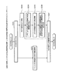
図1は、実施の形態1にかかる光位相歪補償装置の構成例を示す図である。光位相歪補償装置100は、光スプリッタ101、光遅延線102、光検出器(フォトディテクタ:PD)103、低域透過フィルタ(LPF)104、遅延部105、補償信号光源106、光合波器107、を含む。LPF104と遅延部105は、電気信号を扱う制御部110として機能する。
(Embodiment 1)
FIG. 1 is a diagram showing a configuration example of the optical phase distortion compensating device according to the first embodiment. The optical
図中A〜Cは、図1の各箇所でのWDM信号の波形図であり、Aは装置に入力されるWDM信号の波形図であり、(a)はWDM信号の時間−光強度特性、(b)はWDM信号の波長−光強度特性を示す(図12(a),(b)と同様)。Bは光合波器107の出力波形図であり、(c)はWDM信号の波長−光強度特性を示す(図12(c)と同じ)。(d)はWDM信号の時間−光強度変動特性を示す。Cは伝送路Dの波形図であり、WDM信号の時間−光位相変動特性を示す。
In the figure, A to C are waveform diagrams of the WDM signal at each location in FIG. 1, A is a waveform diagram of the WDM signal input to the apparatus, and (a) is the time-light intensity characteristic of the WDM signal. (B) shows the wavelength-light intensity characteristics of the WDM signal (similar to FIGS. 12 (a) and 12 (b)). B is an output waveform diagram of the
図中A(a)波長−光強度特性に示す強度変動(数GHz)と、数十GHzの変調成分を有するWDM信号は、例えば、伝送路Dを介して装置の光スプリッタ101に入力される。光スプリッタ101は、入力されたWDM信号を2分岐する。分岐の一方側には、例えば光ファイバを用いた光遅延線102が設けられ、光遅延線102は、他方の分岐側のLPF104等の遅延量に対応した所定の遅延量を有してWDM信号を光合波器107に出力する。
In the figure, the WDM signal having the intensity fluctuation (several GHz) shown in the wavelength-light intensity characteristic of A (a) and the modulation component of several tens of GHz is input to the
光スプリッタ101の分岐の他方側に設けられるPD103は、WDM信号を電気信号に変換し、LPF104に出力する。LPF104は、入力されたWDM信号の光強度変動の周波数(数GHz)の成分(光位相歪が主に発生する帯域に相当)を抽出する。遅延部105は、LPF104が有する群遅延分の遅延量を調整し、補償信号を出力する。制御部110として機能するLPF104と遅延部105は、LPF104により帯域制限された強度変動を持つWDM信号の波長帯とは異なる波長の補償信号光を生成する。
The
補償信号光源106は、遅延部105から入力された補償信号より反転増幅器等を用いて生成する逆相の補償信号に基づき、装置に入力されたWDM信号が有する低速(数GHz)な光強度変動の逆相の光強度変動を持つ補償信号光Xを生成する。補償信号光Xは、光源を逆相の補償信号で直接変調する、または連続発振する光源の出力を逆相の補償信号で外部変調器により変調することで生成される。補償信号光Xは、例えば、図中B(c)に示すように、WDM信号の通信波長帯域外に設定する(設定例は後述する)。
The compensation
光合波器107は、分岐の一方側の光遅延線102のWDM信号と、分岐の他方側の補償信号光源106の補償信号光Xとを合波したWDM信号を装置外部の伝送路Dに出力する。
The
図1に記載の各構成のうち、制御部110として機能し、電気信号処理を行うLPF104、遅延部105は、それぞれの機能を有するアナログ回路やFPGA(Field−Programmable Gate Array)で構成できる。また、CPUおよびメモリ等のハードウェアを用いても構成でき、PD103からの入力部、および補償信号光源106に対する出力部にAD変換器、DA変換器を設ければよい。CPUを用いる場合、メモリに格納されたプログラムを実行し、この際メモリの一部を作業領域に用いることで、上記機能を実現できる。
Of the configurations shown in FIG. 1, the
図2は、実施の形態1にかかる光位相歪補償装置による光位相歪の補償の処理を説明するフローチャートである。図1の構成に対応する動作内容を示している。はじめに、装置に入力されるWDM信号は、光スプリッタ101により2分岐される(ステップS201)。分岐された一方のWDM信号は、光遅延線102によりフィルタ(LPF104等)の群遅延分の遅延が調整され、光合波器107に出力される(ステップS202)。
FIG. 2 is a flowchart illustrating a process of compensating for optical phase distortion by the optical phase distortion compensating device according to the first embodiment. The operation contents corresponding to the configuration of FIG. 1 are shown. First, the WDM signal input to the apparatus is split into two by the optical splitter 101 (step S201). One of the branched WDM signals is adjusted for a delay corresponding to the group delay of the filter (LPF104 or the like) by the
また、分岐された他方のWDM信号は、PD103により電気信号に変換され(ステップS203)、LPF104に出力される。LPF104は、低速なWDM信号の光強度変動を抽出し(ステップS204)、遅延部105に出力する。遅延部105は、LPF104の群遅延分の遅延を調整し、補償信号を補償信号光源106に出力する(ステップS205)。補償信号光源106は、入力される補償信号より反転増幅器等を用いて生成する逆相の補償信号に基づき、低速なWDM信号の光強度変動の逆相の光強度(強度変動)を持つ補償信号光Xを生成して光合波器107に出力する(ステップS206)。ステップS204〜ステップS206は、制御部110が電気信号により実行処理する。
Further, the other WDM signal branched is converted into an electric signal by PD103 (step S203) and output to LPF104. The
光合波器107は、分岐の一方の光遅延線102から出力されるWDM信号と、分岐の他方のWDM信号に基づき補償信号光源106が出力する補償信号光Xを合波し、装置外部の伝送路Dに出力する(ステップS207)。
The
上記構成の光位相歪補償装置100は、装置外部の伝送路Dを位相変調器として用いる。そして、伝送路D中で生じる光位相歪を補償する補償信号光Xを生成して伝送路Dに送出する。伝送路D中でのWDM信号により生じる光位相歪を補償するように伝送路D中で補償信号光XによりWDM信号に光位相歪を生じさせることで、WDM信号の伝送による光位相歪を抑えることができる。
The optical phase
上記説明のように、装置に入力されたWDM信号の強度変動をPD103で検出し、光信号と逆相の強度変動を持つ補償信号光Xを補償信号光源106で生成し、WDM信号と補償信号光Xを光合波器107で合波する。これにより、装置から出力するWDM信号は、箇所Bの(d)に示すように、光強度変動が抑えられる(数GHz未満)。そして、箇所Cの(e)に示すように、伝送路Dにおける光位相変動(光位相歪)を抑えることができる。
As described above, the PD103 detects the intensity variation of the WDM signal input to the device, and the compensation
実施の形態1によれば、光ファイバ等の伝送路を位相変調器として用い、光ファイバによる光−光変調により分布定数的に光位相歪を補償することができるため、挿入損失を低減させ、伝送信号に生じる光位相歪を効果的に補償することができる。 According to the first embodiment, a transmission line such as an optical fiber is used as a phase modulator, and optical phase distortion can be compensated for in a distributed constant by optical-optical modulation by the optical fiber, so that the insertion loss can be reduced. It is possible to effectively compensate for the optical phase distortion that occurs in the transmitted signal.
(実施の形態2)
図3は、実施の形態2にかかる光位相歪補償装置の構成例を示す図である。実施の形態2において、実施の形態1(図1)と同一の構成部には同一の符号を付している。実施の形態2では、光位相歪補償装置100が光ファイバ(高屈折率差導波路や高非線形係数媒質を用いた非線形光学媒質)301を介してWDM信号を伝送路Dに出力する。Cは光ファイバ301の出力波形図、D’は伝送路Dの出力波形図である。
(Embodiment 2)
FIG. 3 is a diagram showing a configuration example of the optical phase distortion compensating device according to the second embodiment. In the second embodiment, the same components as those in the first embodiment (FIG. 1) are designated by the same reference numerals. In the second embodiment, the optical
図4は、実施の形態2にかかる光位相歪補償装置による光位相歪の補償の処理を説明するフローチャートである。図3の構成に対応する動作内容を示している。はじめに、光位相歪補償装置100に入力されるWDM信号は、光スプリッタ101により2分岐される(ステップS401)。分岐された一方のWDM信号は、光遅延線102によりフィルタ(LPF104等)の群遅延分の遅延が調整され、光合波器107に出力される(ステップS402)。
FIG. 4 is a flowchart illustrating a process of compensating for optical phase distortion by the optical phase distortion compensating device according to the second embodiment. The operation contents corresponding to the configuration of FIG. 3 are shown. First, the WDM signal input to the optical
また、分岐された他方のWDM信号は、PD103により電気信号に変換され(ステップS403)、LPF104に出力される。LPF104は、低速なWDM信号の光強度変動を抽出し(ステップS404)、遅延部105に出力する。遅延部105は、LPF104の群遅延分の遅延を調整し、補償信号を補償信号光源106に出力する(ステップS405)。補償信号光源106は、入力される補償信号より反転増幅器等を用いて生成する逆相の補償信号に基づき、低速なWDM信号の光強度変動の逆相の光強度(強度変動)を持つ補償信号光Xを生成して光合波器107に出力する(ステップS406)。ステップS404〜ステップS406は、制御部110が電気信号により実行処理する。
Further, the other WDM signal branched is converted into an electric signal by PD103 (step S403) and output to LPF104. The
光合波器107は、分岐の一方の光遅延線102から出力されるWDM信号と、分岐の他方のWDM信号に基づき補償信号光源106が出力する補償信号光Xを合波し、光ファイバ301に出力する(ステップS407)。光ファイバ301は、補償信号光Xによる光ファイバ301内での相互位相変調によりWDM信号に光位相変動を付加して装置外部の伝送路Dに出力する(ステップS408)。
The
上記構成の光位相歪補償装置100は、装置内の光ファイバ301を位相変調器として用いる。そして、伝送路D中で生じる光位相歪を補償する補償信号光Xを生成して光ファイバ301に送出する。伝送路D中でのWDM信号により生じる光位相歪を補償するように、装置内の光ファイバ301で補償信号光Xにより光位相歪を生じさせることで、伝送路DでのWDM信号の伝送による光位相歪を抑えることができる。
The optical phase
光位相歪補償装置100から出力する補償信号光Xを含むWDM信号は、箇所Bの(d)に示すように、光位相歪補償装置100に入力されたWDM信号(a)の逆相を有する。そして、箇所Cの(e)に示すように、光ファイバ301内で相互位相変調により光位相歪を生じさせる。これにより、箇所D’の(f)に示すように伝送路Dにおける光位相変動(光位相歪)を抑えることができる。
The WDM signal including the compensation signal light X output from the optical phase
実施の形態2によれば、装置内に光ファイバ等の非線形光学媒質を設けて、光ファイバによる光−光変調により分布定数的に光位相歪を発生させることで、伝送路に対して光位相歪を除去したWDM信号を出力する。実施の形態2においても挿入損失を低減させ、伝送信号に生じる光位相歪を効果的に補償することができる。 According to the second embodiment, a non-linear optical medium such as an optical fiber is provided in the apparatus, and optical phase distortion is generated in a distributed constant by optical-optical modulation by the optical fiber, thereby causing optical phase with respect to the transmission path. The WDM signal with the distortion removed is output. Also in the second embodiment, the insertion loss can be reduced and the optical phase distortion generated in the transmission signal can be effectively compensated.
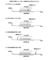
図5は、各実施の形態において用いる補償信号光の設定例を示す図である。補償信号光Xは、WDM信号に影響を与えない各種周波数(波長)に設定することができる。 FIG. 5 is a diagram showing a setting example of the compensation signal light used in each embodiment. The compensation signal light X can be set to various frequencies (wavelengths) that do not affect the WDM signal.
例えば、図5(a)のように、補償信号光Xは、通信波長帯内において、WDM信号の各チャネルの間に設定することができる。また、図5(b)のように、補償信号光XをWDM信号の空きチャネルに設定することができる。また、図5(c)のように、補償信号光XをWDM信号の通信波長帯域外(通信波長帯外)の短波長側に設定することができる。また、図5(d)のように、補償信号光XをWDM信号の通信波長帯域外(通信波長帯外)の長波長側に設定することができる。 For example, as shown in FIG. 5A, the compensation signal light X can be set between each channel of the WDM signal in the communication wavelength band. Further, as shown in FIG. 5B, the compensation signal light X can be set as an empty channel of the WDM signal. Further, as shown in FIG. 5C, the compensation signal light X can be set on the short wavelength side outside the communication wavelength band (outside the communication wavelength band) of the WDM signal. Further, as shown in FIG. 5D, the compensation signal light X can be set on the long wavelength side outside the communication wavelength band (outside the communication wavelength band) of the WDM signal.
(実施の形態3)
図6は、実施の形態3にかかる光位相歪補償装置の構成例を示す図である。実施の形態3では、伝送路D中でのWDM信号の光強度変動、およびWDM信号の種類等の変化に対応する構成である。
(Embodiment 3)
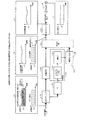
FIG. 6 is a diagram showing a configuration example of the optical phase distortion compensating device according to the third embodiment. In the third embodiment, the configuration corresponds to changes in the light intensity of the WDM signal in the transmission line D, changes in the type of the WDM signal, and the like.
制御部110は、LPF104、遅延部105のほかに、制御回路601、ルックアップテーブル(LUT)602を含む。また、光合波器107の後段には、光ファイバ301との間に光スプリッタ2(603)を設け、PD2(604)で光強度を検出する。PD2(604)の出力は、LPF2(605)を介して制御部110の制御回路601に入力される。なお、101は光スプリッタ1とし、103はPD1、104はLPF1とする。LUT602は、例えば、メモリを用いて構成でき、メモリに設定内容を記憶保持できる。
The
LUT602には、伝送路Dや、伝送するWDM信号の種類に応じたLPF104,605の帯域幅、遅延部105の遅延量、補償信号の波長およびチャープ量が設定される。制御回路601は、光スプリッタ2(603)〜LPF2(605)のフィードバック(FB)系統の出力により、光合波器107で合波したWDM信号と補償信号光Xの光信号をモニタし、補償信号光Xの強度を調整する。また、制御回路601は、WDM信号が経由する伝送路Dの変化(光ファイバの分散特性や損失の変化)や、WDM信号のチャネル数、チャネル間隔が変化した場合に、LUT602の設定を参照して、補償信号の各パラメータを再設定する。
In the
図7は、実施の形態3にかかる光位相歪補償装置による光位相歪の補償の処理を説明するフローチャートである。図6の構成に対応する動作内容を示している。はじめに、光位相歪補償装置100に入力されるWDM信号は、光スプリッタ1(101)により2分岐される(ステップS701)。分岐された一方のWDM信号は、光遅延線102によりフィルタ(LPF1(104))の群遅延分の遅延が調整され、光合波器107に出力される(ステップS702)。
FIG. 7 is a flowchart illustrating a process of compensating for optical phase distortion by the optical phase distortion compensating device according to the third embodiment. The operation contents corresponding to the configuration of FIG. 6 are shown. First, the WDM signal input to the optical
また、分岐された他方のWDM信号は、PD1(103)により電気信号に変換され(ステップS703)、LPF1(104)に出力される。LPF1(104)は、低速なWDM信号の光強度変動を抽出し(ステップS704)、遅延部105に出力する。遅延部105は、LPF1(104)の群遅延分の遅延を調整し、補償信号を補償信号光源106に出力する(ステップS705)。補償信号光源106は、入力される補償信号より反転増幅器等を用いて生成する逆相の補償信号に基づき、低速なWDM信号の光強度変動の逆相の光強度(強度変動)を持つ補償信号光Xを生成して光合波器107に出力する(ステップS706)。ステップS704〜ステップS706、ステップS710、ステップS711、ステップS712、ステップS713、ステップS715は、制御部110が電気信号により実行処理する。
Further, the other branched WDM signal is converted into an electric signal by PD1 (103) (step S703) and output to LPF1 (104). LPF1 (104) extracts the light intensity fluctuation of the low-speed WDM signal (step S704) and outputs it to the
光合波器107は、分岐の一方の光遅延線102から出力されるWDM信号と、分岐の他方のWDM信号に基づき補償信号光源106が出力する補償信号光Xを合波し、光ファイバ301に出力する(ステップS707)。光ファイバ301は、補償信号光Xによる光ファイバ301内での相互位相変調によりWDM信号に光位相変動を付加して装置外部の伝送路Dに出力する。
The
光位相歪補償装置100が出力するWDM信号は光スプリッタ2(603)で分岐され(ステップS708)、PD2(604)で電気信号に変換される(ステップS709)。PD2(604)の出力により、LPF2(605)が低速な光強度変動を抽出し、制御部110の制御回路601に出力する(ステップS710)。
The WDM signal output by the optical
制御回路601は、LPF2(605)から入力される光強度変動が最小であるかを判断する(ステップS711)。例えば、LPF2(605)から入力される光強度変動は時間とともに変動するがこの変動量が前回値よりも低いかを判断する。そして、制御回路601は、光強度変動が最小であれば(ステップS711:Yes)、FB制御を完了する。一方、光強度変動が最小でなければ(ステップS711:No)、遅延部105に対する遅延量を変化させる調整を行い(ステップS712)、補償信号光源106に対する光強度を変化させる調整を行う(ステップS713)。
The
ステップS712の調整により、次回制御においてステップS705の遅延量が調整され、ステップS713の調整により、次回制御においてステップS706の補償信号光Xの光強度が調整される。 The adjustment in step S712 adjusts the delay amount in step S705 in the next control, and the adjustment in step S713 adjusts the light intensity of the compensation signal light X in step S706 in the next control.
また、制御回路601は、光位相歪補償装置100の外部からWDM信号が経由する伝送路Dが変化した場合や、WDM信号のチャネル数、チャネル間隔が変化した場合に、LUT602を再設定する(ステップS714)。この際、LUT602に設定される補償信号の各パラメータ(LPF1,2(104,605))の帯域幅(ステップS715)、遅延部105の遅延量(ステップS712)、補償信号光源106の光強度(ステップS713)、がそれぞれ再設定される。ステップS715の調整により、次回制御においてステップS704,ステップS710におけるLPF1,2(104,605)の帯域幅が調整される。
Further, the
実施の形態3によれば、実施の形態1,2同様の作用効果を有する。そして、実施の形態2同様に装置内に光ファイバ等の非線形光学媒質を設けて、光ファイバによる光−光変調により分布定数的に光位相歪を発生させることで、伝送路に対して光位相歪を除去したWDM信号を出力する。 According to the third embodiment, it has the same function and effect as those of the first and second embodiments. Then, as in the second embodiment, a non-linear optical medium such as an optical fiber is provided in the apparatus, and optical phase distortion is generated in a distributed constant by optical-optical modulation by the optical fiber, so that the optical phase is optical with respect to the transmission path. The WDM signal with the distortion removed is output.
加えて、実施の形態3では、装置から出力するWDM信号をフィードバック制御して、WDM信号の光強度変動を抑える制御を行う。これにより、WDM信号の伝送路や伝送信号の種類の変化、例えば、伝送信号のチャネル数やチャネル間隔の変動に対応して、LPFの帯域幅、遅延量、補償信号光の波長やチャープ量を調整し、WDM信号の光強度変動(光位相歪)を抑えることができる。そして、伝送路の前段に光変調用の光ファイバを挿入する構成において、光ファイバのゼロ分散と補償信号光の波長を調整することで効果的に光位相歪を補償できるようになる。 In addition, in the third embodiment, the WDM signal output from the apparatus is feedback-controlled to suppress fluctuations in the light intensity of the WDM signal. As a result, the LPF bandwidth, delay amount, compensation signal light wavelength and chapter amount can be adjusted in response to changes in the transmission path of the WDM signal and the type of transmission signal, for example, changes in the number of channels and channel spacing of the transmission signal. It can be adjusted to suppress fluctuations in the light intensity (light phase distortion) of the WDM signal. Then, in a configuration in which an optical fiber for optical modulation is inserted in front of the transmission line, the optical phase distortion can be effectively compensated by adjusting the zero dispersion of the optical fiber and the wavelength of the compensation signal light.
(実施の形態4)
図8は、実施の形態4にかかる光位相歪補償装置の構成例を示す図である。実施の形態4では、実施の形態3の構成に加えて、伝送路中での低速な光強度変動に対応した制御を行い、光位相歪をより低減させる構成である。
(Embodiment 4)
FIG. 8 is a diagram showing a configuration example of the optical phase distortion compensating device according to the fourth embodiment. In the fourth embodiment, in addition to the configuration of the third embodiment, the control corresponding to the low-speed fluctuation of the light intensity in the transmission line is performed to further reduce the optical phase distortion.
PD1(103)の出力は、制御部110内のディバイダ1(801)で分岐され、一方はLPF1(104a)側に出力され、他方はLPF2(104b)側に出力される。
The output of PD1 (103) is branched by the divider 1 (801) in the
一方側のLPF1(104a)と、他方側のLPF2(104b)は同一または異なる透過帯域を有している。一方側の系統では、LPF1(104a)の透過帯域に基づき遅延部1(105a)で遅延させ、補償信号光源1(106a)から補償信号光X1を出力する。他方側の系統では、LPF2(104b)の透過帯域に基づき遅延部2(105b)で遅延させ、補償信号光源2(106b)から補償信号光X1と異なる波長の補償信号光X2を出力する。LPF1,2(104a,104b)は、例えば、WDM信号全体の位相歪に対応する透過特性とWDM信号から波長に対して一つ置きに間引いたWDM信号の位相歪に対応する透過特性を有する。
The LPF1 (104a) on the one side and the LPF2 (104b) on the other side have the same or different transmission bands. In the system on one side, the delay unit 1 (105a) delays based on the transmission band of the LPF 1 (104a), and the compensation signal light X1 is output from the compensation signal light source 1 (106a). In the system on the other side, the delay unit 2 (105b) delays the LPF2 (104b) based on the transmission band, and the compensation signal light source 2 (106b) outputs the compensation signal light X2 having a wavelength different from that of the compensation signal light X1. The
また、制御部110は、上記2つの補償信号光X1,X2の生成に関連して、FB系統も2系統を有する。制御部110は、PD2(604)の出力をディバイダ2(802)で分岐する。分岐した一方の出力は、LPF3(605a)を介して制御回路601に出力され、他方の出力は、LPF4(605b)を介して制御回路601に出力される。LPF3(605a)は、LPF1(104a)と同じ透過帯域を有し、LPF4(605b)は、LPF2(104b)と同じ透過帯域を有する。
Further, the
図9は、実施の形態4にかかる2つの補償信号光の設定例を示す図である。補償信号光X1、X2は、WDM信号に影響を与えない各種周波数(波長)に設定することができる。 FIG. 9 is a diagram showing a setting example of the two compensation signal lights according to the fourth embodiment. The compensation signal lights X1 and X2 can be set to various frequencies (wavelengths) that do not affect the WDM signal.
例えば、図9(a)のように、補償信号光X1,X2をいずれもWDM信号の通信波長帯域外(通信波長帯外)の短波長側に設定することができる。また、図9(b)のように、補償信号光X1,X2をいずれもWDM信号の通信波長帯域外(通信波長帯外)の長波長側に設定することができる。また、図9(c)のように、補償信号光X1,X2をWDM信号の通信波長帯域外(通信波長帯外)とし、補償信号光X1をWDM信号の通信波長帯域外の短波長側に設定し、補償信号光X2をWDM信号の通信波長帯域外の長波長側に設定することができる。 For example, as shown in FIG. 9A, both the compensation signal lights X1 and X2 can be set on the short wavelength side outside the communication wavelength band (outside the communication wavelength band) of the WDM signal. Further, as shown in FIG. 9B, both the compensation signal lights X1 and X2 can be set on the long wavelength side outside the communication wavelength band (outside the communication wavelength band) of the WDM signal. Further, as shown in FIG. 9C, the compensation signal lights X1 and X2 are set outside the communication wavelength band of the WDM signal (outside the communication wavelength band), and the compensation signal light X1 is set on the short wavelength side outside the communication wavelength band of the WDM signal. It can be set and the compensation signal light X2 can be set on the long wavelength side outside the communication wavelength band of the WDM signal.
実施の形態4によれば、実施の形態1〜3同様の作用効果を有する。加えて、実施の形態4では、装置から出力するWDM信号をフィードバック制御して、WDM信号の光強度変動を抑え、さらに、2つの異なる透過特性のLPFを用いて2つの異なる波長の補償信号光を出力する。例えば、LPFをアナログ回路で構成した場合、一つのLPFだけでは任意の透過特性を得ることができず、上述したWDM信号の強度変動の特性に十分対応できない。しかし、上記のように、LPFを複数用いて補償信号光を合波することで、WDM信号の強度変動の特性に対応できるようになる。 According to the fourth embodiment, it has the same effect as that of the first to third embodiments. In addition, in the fourth embodiment, the WDM signal output from the apparatus is feedback-controlled to suppress the fluctuation of the light intensity of the WDM signal, and further, the compensation signal light of two different wavelengths is used by using the LPF having two different transmission characteristics. Is output. For example, when the LPF is composed of an analog circuit, it is not possible to obtain an arbitrary transmission characteristic with only one LPF, and it is not possible to sufficiently cope with the above-mentioned characteristic of intensity fluctuation of the WDM signal. However, as described above, by using a plurality of LPFs to combine the compensation signal light, it becomes possible to cope with the characteristics of the intensity fluctuation of the WDM signal.
そして、実施の形態4では、伝送路中でWDM信号の低速な光強度信号は一定ではなく変化することに対応し、異なる波長の補償信号光を出力することで、波長分散により光強度変動を変化させることができる。これにより、伝送路中で生じる光位相歪をより低減させることができるようになる。 Then, in the fourth embodiment, the low-speed light intensity signal of the WDM signal is not constant and changes in the transmission line, and the compensation signal light of different wavelengths is output to cause the light intensity to fluctuate due to wavelength dispersion. Can be changed. This makes it possible to further reduce the optical phase distortion that occurs in the transmission line.
(実施の形態5)
図10は、実施の形態5にかかる光位相歪補償装置の構成例を示す図である。実施の形態5では、実施の形態4と同様に、伝送路中での低速な光強度変動に対応した制御を行い、光位相歪をより低減させる構成であり、2系統のLPF1,2の前段の構成が異なる。
(Embodiment 5)
FIG. 10 is a diagram showing a configuration example of the optical phase distortion compensating device according to the fifth embodiment. In the fifth embodiment, as in the fourth embodiment, the control corresponding to the low-speed fluctuation of the light intensity in the transmission line is performed to further reduce the optical phase distortion, and the pre-stages of the two LPFs 1 and 2 are configured. The composition of is different.
実施の形態5では、実施の形態4の構成に加えて、光スプリッタ3(1001)と、光フィルタ1,2(1002a,1002b)と、PD1a,1b(103a,103b)とを含む。
In the fifth embodiment, in addition to the configuration of the fourth embodiment, the optical splitter 3 (1001), the
光スプリッタ3(1001)は、光スプリッタ1(101)が出力するWDN信号の光を2分岐する。分岐された一方には、所定の透過波長を有する光フィルタ1(1002a)が設けられ、PD1a(103a)で検出される。PD1a(103a)の出力は、LPF1(104a)に入力される。分岐された他方には、光フィルタ1(1002a)と異なる透過波長を有する光フィルタ2(1002b)が設けられ、PD1b(103b)で検出される。PD1b(103b)の出力は、LPF2(104b)に入力される。 The optical splitter 3 (1001) splits the light of the WDN signal output by the optical splitter 1 (101) into two. An optical filter 1 (1002a) having a predetermined transmission wavelength is provided on one of the branches, and the light filter 1 (1002a) is detected by the PD1a (103a). The output of PD1a (103a) is input to LPF1 (104a). On the other side of the branch, an optical filter 2 (1002b) having a transmission wavelength different from that of the optical filter 1 (1002a) is provided and detected by the PD1b (103b). The output of PD1b (103b) is input to LPF2 (104b).
実施の形態5によれば、実施の形態4と同様の作用効果を有する。さらに、実施の形態5では、光フィルタ1,2(1002a,1002b)によりWDM信号に対し、光波長別に異なる透過特性を有してLPF1,2(104a,104b)による透過を行う。これにより、LPF1,2(104a,104b)の透過特性に加えて、光フィルタ1,2(1002a,1002b)の透過特性により、異なる2つの補償信号光X1,X2を生成でき、透過特性を多様化できる。また、LPF1,2(104a,104b)がアナログ回路で構成した場合でも、任意の透過特性を得ることができるようになる。これにより、実施の形態5によれば、伝送路中で生じる光位相歪を実施の形態4よりもさらに効果的に補償できるようになる。
According to the fifth embodiment, it has the same effect as that of the fourth embodiment. Further, in the fifth embodiment, the
(実施の形態6)
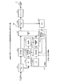
図11は、実施の形態6にかかる光位相歪補償装置の構成例を示す図である。実施の形態6では、実施の形態5と同様に、伝送路中での低速な光強度変動に対応した制御を行い、さらに偏波多重されたWDM信号に対応して光位相歪をより低減させる構成である。
(Embodiment 6)
FIG. 11 is a diagram showing a configuration example of the optical phase distortion compensating device according to the sixth embodiment. In the sixth embodiment, as in the fifth embodiment, control is performed in response to low-speed optical intensity fluctuations in the transmission line, and optical phase distortion is further reduced in response to the WDM signal in which polarization multiplexing is performed. It is a composition.
実施の形態6では、実施の形態5と異なる構成として、偏波分離部としての偏波ビームスプリッタ1,2(1101,1102)と、PD3,4(1103a,1103b)と、偏波制御器1,2(1104a,1104b)を設けている。なお、実施の形態5で説明した光スプリッタ3(1001)と、光フィルタ1,2(1002a,1002b)は説明を省略しているが、これらの構成を加えてもよい。
In the sixth embodiment, the
偏波ビームスプリッタ1(1101)は、光スプリッタ1(101)の出力を直交する偏波(H,V)に分離出力する。偏波ビームスプリッタ1(1101)により分離出力されたH偏波成分のWDM信号は、PD1a(103a)に出力され、V偏波成分のWDM信号は、PD1b(103b)に出力される。 The polarization beam splitter 1 (1101) separates and outputs the output of the optical splitter 1 (101) into orthogonal polarizations (H, V). The WDM signal of the H polarization component separated and output by the polarization beam splitter 1 (1101) is output to the PD 1a (103a), and the WDM signal of the V polarization component is output to the PD 1b (103b).
また、FB系統に設けられる偏波ビームスプリッタ2(1102)は、光スプリッタ2(603)の出力を直交する偏波(H,V)に分離出力する。偏波ビームスプリッタ2(1102)により分離出力されたH偏波成分のWDM信号は、PD3(1103a)に出力され、V偏波成分のWDM信号は、PD4(1003b)に出力される。PD3(1103a)の出力は、LPF3(605a)に出力され、PD4(1103b)の出力は、LPF4(605b)に出力される。 Further, the polarization beam splitter 2 (1102) provided in the FB system separates and outputs the output of the optical splitter 2 (603) into orthogonal polarizations (H, V). The WDM signal of the H polarization component separated and output by the polarization beam splitter 2 (1102) is output to the PD3 (1103a), and the WDM signal of the V polarization component is output to the PD4 (1003b). The output of PD3 (1103a) is output to LPF3 (605a), and the output of PD4 (1103b) is output to LPF4 (605b).
偏波制御器1(1104a)は、補償信号光源1(106a)が出力する補償信号光X1のH成分の偏波を制御する。偏波制御器2(1104b)は、補償信号光源2(106b)が出力する補償信号光X2のV成分の偏波を制御する。偏波制御器1,2(1104a,1104b)は、補償信号光X1、X2のH成分、V成分の偏波状態を安定化させる。
The polarization controller 1 (1104a) controls the polarization of the H component of the compensation signal light X1 output by the compensation signal light source 1 (106a). The polarization controller 2 (1104b) controls the polarization of the V component of the compensation signal light X2 output by the compensation signal light source 2 (106b). The
実施の形態6によれば、実施の形態5と同様の作用効果を有する。さらに、実施の形態6では、偏波多重されたWDM信号の各偏波成分の光位相歪を補償できるようになる。これにより、実施の形態6によれば、伝送路中で生じる光位相歪を実施の形態5よりもさらに効果的に補償できるようになる。また、実施の形態6で説明した偏波分離は、図11に示した構成に限らず、各実施の形態1〜5に適用することができる。各実施の形態に適用し、補償信号光源を偏波別に設けることで、直交偏波多重されたWDM信号の各偏波別の光位相歪を補償できるようになる。 According to the sixth embodiment, it has the same effect as that of the fifth embodiment. Further, in the sixth embodiment, it becomes possible to compensate for the optical phase distortion of each polarization component of the polarization-multiplexed WDM signal. Thereby, according to the sixth embodiment, the optical phase distortion generated in the transmission line can be compensated more effectively than the fifth embodiment. Further, the polarization separation described in the sixth embodiment is not limited to the configuration shown in FIG. 11, and can be applied to the first to fifth embodiments. By applying to each embodiment and providing a compensation signal light source for each polarization, it becomes possible to compensate for the optical phase distortion for each polarization of the WDM signal multiplexed with orthogonally polarized waves.
以上説明した各実施の形態によれば、光ファイバによる光−光変調を行うことで分布定数的に光位相歪を補償し、広帯域な伝送帯域で発生する光位相歪を補償できる。そして、LN型光位相変調器等の特別な位相変調器を設ける必要がないため挿入損失を低減化できる。実施の形態では、光ファイバまたは伝送路である光ファイバを位相変調器として用い、変調信号である補償信号光をWDM信号と合波して光ファイバ内を伝搬させることで、WDM信号に生じる光位相歪を効果的に補償できる。補償信号光は、伝送するWDM信号の波長を避けた各波長、例えば、短波長、長波長、WDMチャネル間、空きWDMチャネル等に簡単に設定できる。 According to each of the above-described embodiments, the optical phase distortion can be compensated for in a distributed constant by performing optical-optical modulation by an optical fiber, and the optical phase distortion generated in a wide band transmission band can be compensated. Further, since it is not necessary to provide a special phase modulator such as an LN type optical phase modulator, the insertion loss can be reduced. In the embodiment, an optical fiber or an optical fiber which is a transmission path is used as a phase modulator, and the compensation signal light which is a modulation signal is combined with the WDM signal and propagated in the optical fiber to generate light in the WDM signal. Phase distortion can be effectively compensated. The compensation signal light can be easily set at each wavelength avoiding the wavelength of the WDM signal to be transmitted, for example, a short wavelength, a long wavelength, between WDM channels, an empty WDM channel, and the like.
より具体的には、伝送するWDM信号の強度変動を検出し、逆相の強度変動を持つ補償信号光を生成し、WDM信号と補償信号光とを合波して、伝送路である光ファイバを伝送するWDM信号に付加的な損失を与えることなく光位相歪を補償する。また、補償信号光の波長やチャープ等を調整することで、より効果的に光位相歪を補償できるようになる。また、合波後のWDM信号をモニタし、フィードバック制御することで、WDM信号の光強度の時間的な変動に対応して補償信号光の光強度を適切に調整できるようになる。また、異なる波長の複数の補償信号光を生成し、WDM信号に合波する構成により、LPFや光フィルタの透過特性を組み合わせて、任意の特性(入力されるWDM信号の強度変動の逆相)を有する補償信号光を生成でき、光位相歪を効果的に補償できる。 More specifically, an optical fiber which is a transmission path by detecting an intensity fluctuation of a WDM signal to be transmitted, generating a compensating signal light having an intensity variation of the opposite phase, and combining the WDM signal and the compensating signal light. Compensates for optical phase distortion without inflicting additional loss on the WDM signal being transmitted. Further, by adjusting the wavelength, chirp, etc. of the compensation signal light, the optical phase distortion can be compensated more effectively. Further, by monitoring the WDM signal after the combined wave and controlling the feedback, the light intensity of the compensation signal light can be appropriately adjusted in response to the temporal fluctuation of the light intensity of the WDM signal. In addition, by generating multiple compensation signal lights of different wavelengths and combining them with the WDM signal, the transmission characteristics of the LPF and optical filter can be combined to create arbitrary characteristics (reverse phase of intensity fluctuation of the input WDM signal). Compensation signal light can be generated, and optical phase distortion can be effectively compensated.
また、上記実施の形態では、ローパスフィルタ、補償信号光源、さらには光フィルタを2系統設けて異なる2波長の補償信号光を生成する構成とした。これに限らず、補償信号光として3以上の異なる波長を生成する構成としてもよく、さらに光位相歪を効果的に抑制できるようになる。 Further, in the above embodiment, a low-pass filter, a compensation signal light source, and two optical filters are provided to generate compensation signal light having two different wavelengths. Not limited to this, the configuration may be such that three or more different wavelengths are generated as the compensation signal light, and the optical phase distortion can be effectively suppressed.
なお、本実施の形態で説明した光位相歪補償方法は、予め用意された制御プログラムを対象機器(上記光位相歪補償装置)等のコンピュータ(CPU等)が実行することにより実現することができる。本制御プログラムは、磁気ディスク、光ディスク、USB(Universal Serial Bus)フラッシュメモリなどのコンピュータで読み取り可能な記録媒体に記録され、コンピュータによって記録媒体から読み出されることによって実行される。また、制御プログラムは、インターネット等のネットワークを介して配布してもよい。 The optical phase distortion compensation method described in the present embodiment can be realized by executing a control program prepared in advance by a computer (CPU or the like) such as a target device (the optical phase distortion compensation device). .. This control program is recorded on a computer-readable recording medium such as a magnetic disk, an optical disk, or a USB (Universal Serial Bus) flash memory, and is executed by being read from the recording medium by the computer. Further, the control program may be distributed via a network such as the Internet.
上述した実施の形態に関し、さらに以下の付記を開示する。 The following additional notes are further disclosed with respect to the above-described embodiment.
(付記1)入力される波長多重された光信号の光位相歪を補償する光位相歪補償装置において、
前記光信号の強度変動を検出する検出部と、
前記強度変動の成分から光位相歪が主に発生する帯域を抽出するフィルタと、
前記フィルタの抽出に基づき、入力される光信号の時間的な強度変動を有する補償信号を生成する制御部と、
前記制御部の補償信号に基づき、前記強度変動に対して逆相の強度変動を有し、前記光信号の波長と異なる波長の補償信号光を出力する補償信号光源と、
前記光信号と前記補償信号光とを合波した信号光を伝送路へ出力し、当該伝送路で光位相変調を生じさせる光合波器と、
を備えたことを特徴とする光位相歪補償装置。
(Appendix 1) In an optical phase distortion compensator that compensates for optical phase distortion of an input wavelength-multiplexed optical signal.
A detection unit that detects fluctuations in the intensity of the optical signal,
A filter that extracts the band in which optical phase distortion mainly occurs from the intensity fluctuation component, and
Based on the extraction of the filter, a control unit that generates a compensation signal having a temporal intensity variation of the input optical signal, and a control unit.
Based on the compensation signal of the control unit, a compensation signal light source that has an intensity variation of the opposite phase to the intensity variation and outputs a compensation signal light having a wavelength different from the wavelength of the optical signal, and a compensation signal light source.
An optical combiner that outputs a signal light obtained by combining the optical signal and the compensation signal light to a transmission line and causes optical phase modulation in the transmission line.
An optical phase distortion compensator characterized by being equipped with.
(付記2)前記光合波器の出力に接続された非線形媒質を有し、
前記非線形媒質で光位相変調を生じさせることを特徴とする付記1に記載の光位相歪補償装置。
(Appendix 2) Having a non-linear medium connected to the output of the optical combiner,
The optical phase distortion compensator according to
(付記3)前記フィルタは、時間的に低速な前記光信号の強度変動を検出するローパスフィルタであることを特徴とする付記1または2に記載の光位相歪補償装置。
(Supplementary Note 3) The optical phase distortion compensating device according to
(付記4)入力される前記光信号を分岐する光分岐部と、
前記光分岐部で分岐された一方に設けられ、前記光信号を所定量遅延させる光遅延線と、
前記光分岐部で分岐された他方に前記検出部と前記フィルタを設け、
前記フィルタの出力を所定量遅延させ、前記光信号の遅延量と整合させた前記補償信号を前記補償信号光源に出力する遅延部と、を有することを特徴とする付記1〜3のいずれか一つに記載の光位相歪補償装置。
(Appendix 4) An optical branching portion that branches the input optical signal and
An optical delay line provided on one of the branches of the optical branch portion to delay the optical signal by a predetermined amount, and an optical delay line.
The detection unit and the filter are provided on the other side branched by the optical branching unit.
Any one of
(付記5)前記補償信号光光源は、前記補償信号光を、前記光信号の使用チャネル以外、前記光チャネルの空きチャネル、前記光信号の通信波長帯域外、の少なくとも一つの所定の波長で出力することを特徴とする付記1〜4のいずれか一つに記載の光位相歪補償装置。
(Appendix 5) The compensating signal optical light source outputs the compensating signal light at at least one predetermined wavelength other than the channel used for the optical signal, an empty channel of the optical channel, or outside the communication wavelength band of the optical signal. The optical phase distortion compensating device according to any one of
(付記6)前記制御部は、
前記光信号が伝送する伝送路の種類、および前記光信号の種類に対応する前記フィルタの帯域幅、前記光信号と前記補償信号光の遅延整合のための遅延量、前記補償信号光の波長およびチャープ量の各設定値を設定保持する設定部を有し、
前記光信号が伝送する伝送路の種類、および前記光信号の種類の入力に基づく前記設定値を用いて前記補償信号を生成することを特徴とする付記1〜5のいずれか一つに記載の光位相歪補償装置。
(Appendix 6) The control unit is
The type of transmission path to which the optical signal is transmitted, the bandwidth of the filter corresponding to the type of optical signal, the amount of delay for delay matching between the optical signal and the compensation signal light, the wavelength of the compensation signal light, and It has a setting unit that sets and holds each set value of the chap amount.
The description according to any one of
(付記7)前記光合波器が出力する前記光信号を分岐する第2光分岐部と、
前記第2光分岐部で分岐された前記光信号の光強度を検出する第2検出器と、
前記第2検出器で検出されたフィードバックの強度変動の成分から光位相歪が主に発生する帯域を抽出する第2フィルタと、を有し、
前記制御部は、前記第2フィルタの出力に基づき、前記補償信号の生成を調整することを特徴とする付記1〜6のいずれか一つに記載の光位相歪補償装置。
(Appendix 7) A second optical branching portion for branching the optical signal output by the optical combiner, and
A second detector that detects the light intensity of the optical signal branched at the second optical branching portion, and
It has a second filter that extracts a band in which optical phase distortion mainly occurs from a component of feedback intensity fluctuation detected by the second detector.
The optical phase distortion compensating device according to any one of
(付記8)前記検出部の出力を分岐するディバイダと、
前記ディバイダで分岐された各系統にそれぞれ複数の前記フィルタと、前記補償信号光源を設け、
前記第2検出器の出力を分岐する第2ディバイダと、
前記ディバイダで分岐された各系統にそれぞれ複数の第2フィルタを設け、
前記制御部は、複数の前記フィルタおよび複数の補償信号光源を制御し、複数の補償信号光源に対し複数の異なる補償信号光を出力させる制御信号を出力し、
複数の前記第2フィルタの出力に基づき、複数の前記補償信号の生成を調整することを特徴とする付記7に記載の光位相歪補償装置。
(Appendix 8) A divider that branches the output of the detector and
A plurality of the filters and the compensation signal light source are provided in each system branched by the divider.
A second divider that branches the output of the second detector,
A plurality of second filters are provided for each system branched by the divider.
The control unit controls a plurality of the filters and a plurality of compensation signal light sources, and outputs a control signal for outputting a plurality of different compensation signal lights to the plurality of compensation signal light sources.
The optical phase distortion compensating device according to Appendix 7, wherein the generation of the plurality of compensation signals is adjusted based on the outputs of the plurality of second filters.
(付記9)前記光分岐部の出力を光分岐する第2光分岐部と、
前記第2光分岐部で光分岐された各系統にそれぞれ設けられ、前記信号光をそれぞれ異なる波長で透過させる複数の光フィルタと、
複数の光フィルタが出力する光信号の強度変動をそれぞれ検出し、前記フィルタに出力する複数の検出部と、
を備えたことを特徴とする付記8に記載の光位相歪補償装置。
(Appendix 9) A second optical branch portion that optically branches the output of the optical branch portion, and
A plurality of optical filters provided in each system optically branched by the second optical branching portion and transmitting the signal light at different wavelengths, and
A plurality of detectors that detect intensity fluctuations of optical signals output by a plurality of optical filters and output to the filters, and a plurality of detectors.
The optical phase distortion compensating device according to Appendix 8, wherein the optical phase distortion compensating device is provided.
(付記10)前記光分岐部の出力を直交する偏波別に分離出力する偏波分離部と、
複数の前記補償信号光源と、を設け、
前記制御部は、
複数の前記補償信号光源に対し、偏波別の補償信号光を出力させることを特徴とする付記1〜9のいずれか一つに記載の光位相歪補償装置。
(Appendix 10) A polarization separation unit that separates and outputs the output of the optical branching unit for each orthogonal polarization, and a polarization separation unit.
A plurality of the compensation signal light sources and the above-mentioned compensation signal light sources are provided.
The control unit
The optical phase distortion compensating device according to any one of
(付記11)前記第2光分岐部の出力を直交する偏波別に分離出力する第2偏波分離部と、
前記第2偏波分離部の各偏波別の出力を検出する複数の第2検出部と、を有し、
前記制御部は、前記第2検出部に接続された各偏波別の複数の第2フィルタの出力に基づき、複数の前記補償信号の生成を偏波別に調整することを特徴とする付記10に記載の光位相歪補償装置。
(Appendix 11) A second polarization separating section that separates and outputs the output of the second optical branching section according to orthogonal polarizations, and a second polarization separating section.
It has a plurality of second detection units for detecting the output of each polarization of the second polarization separation unit.
Addendum 10 is characterized in that the control unit adjusts the generation of the plurality of compensation signals for each polarization based on the outputs of the plurality of second filters for each polarization connected to the second detection unit. The optical phase distortion compensator according to the description.
(付記12)入力される波長多重された光信号の光位相歪を補償する光位相歪補償方法において、
前記光信号の強度変動を検出し、
前記強度変動の成分から光位相歪が主に発生する帯域を抽出し、
前記抽出に基づき、入力される光信号の時間的な強度変動を有する補償信号を生成し、
前記補償信号に基づき、前記強度変動に対して逆相の強度変動を有し、前記光信号の波長と異なる波長の補償信号光を出力し、
前記光信号と前記補償信号光とを合波した信号光を伝送路へ出力し、当該伝送路で光位相変調を生じさせる、
ことを特徴とする光位相歪補償方法。
(Appendix 12) In an optical phase distortion compensation method for compensating for optical phase distortion of an input wavelength-multiplexed optical signal.
The intensity fluctuation of the optical signal is detected and
The band in which the optical phase distortion mainly occurs is extracted from the component of the intensity fluctuation, and the band is extracted.
Based on the above extraction, a compensation signal having a temporal intensity variation of the input optical signal is generated.
Based on the compensation signal, the compensation signal light having an intensity variation of the opposite phase to the intensity variation and having a wavelength different from the wavelength of the optical signal is output.
A signal light obtained by combining the optical signal and the compensation signal light is output to a transmission line, and optical phase modulation is generated in the transmission line.
An optical phase distortion compensation method characterized by this.
(付記13)前記抽出は、前記光信号を低域濾過することで、時間的に低速な前記光信号の強度変動を検出することを特徴とする付記12に記載の光位相歪補償方法。 (Appendix 13) The optical phase distortion compensation method according to Appendix 12, wherein the extraction detects intensity fluctuations of the optical signal, which is slow in time, by filtering the optical signal in a low frequency range.
(付記14)前記補償信号光は、前記光信号の使用チャネル間、前記光チャネルの空きチャネル、前記光信号の通信波長帯域外、の少なくとも一つの所定の波長であることを特徴とする付記12または13に記載の光位相歪補償方法。 (Supplementary note 14) The compensating signal light is at least one predetermined wavelength between the channels used for the optical signal, an empty channel of the optical channel, and outside the communication wavelength band of the optical signal. Alternatively, the optical phase distortion compensation method according to 13.
100 光位相歪補償装置
101,603,1001 光スプリッタ
102 光遅延線
103,103a,103b,604,1103a,1103b 光検出器(PD)
104,104a,104b,605,605a,605b 低域透過フィルタ(LPF)
105,105a,105b 遅延部
106,106a,106b 補償信号光源
107 光合波器
110 制御部
301 光ファイバ(非線形光学媒質)
601 制御回路
602 ルックアップテーブル(LUT)
801,802 ディバイダ
1002a,1002b 光フィルタ
1101,1102 偏波ビームスプリッタ
D 伝送路
X,X1,X2 補償信号光
100 Optical
104, 104a, 104b, 605, 605a, 605b Low Pass Filter (LPF)
105, 105a,
601
801,802
Claims (11)
前記光信号の強度変動を検出する検出部と、
前記強度変動の成分から光位相歪が主に発生する帯域を抽出するフィルタと、
前記フィルタの抽出に基づき、入力される光信号の時間的な強度変動を有する補償信号を生成する制御部と、
前記制御部の補償信号に基づき、前記強度変動に対して逆相の強度変動を有し、前記光信号の波長と異なる波長の補償信号光を出力する補償信号光源と、
前記光信号と前記補償信号光とを合波した信号光を伝送路へ出力する光合波器と、
前記光合波器の出力に接続された非線形媒質と、を有し、
前記非線形媒質で光位相変調を生じさせることを特徴とする光位相歪補償装置。 In an optical phase distortion compensator that compensates for the optical phase distortion of an input wavelength-multiplexed optical signal,
A detection unit that detects fluctuations in the intensity of the optical signal,
A filter that extracts the band in which optical phase distortion mainly occurs from the intensity fluctuation component, and
Based on the extraction of the filter, a control unit that generates a compensation signal having a temporal intensity variation of the input optical signal, and a control unit.
Based on the compensation signal of the control unit, a compensation signal light source that has an intensity variation of the opposite phase to the intensity variation and outputs a compensation signal light having a wavelength different from the wavelength of the optical signal, and a compensation signal light source.
An optical combiner that outputs a signal light obtained by combining the optical signal and the compensation signal light to a transmission line, and
With a non-linear medium connected to the output of the optical combiner,
An optical phase distortion compensator for causing optical phase modulation in the nonlinear medium.
前記光分岐部で分岐された一方に設けられ、前記光信号を所定量遅延させる光遅延線と、
前記光分岐部で分岐された他方に前記検出部と前記フィルタを設け、
前記フィルタの出力を所定量遅延させ、前記光信号の遅延量と整合させた前記補償信号を前記補償信号光源に出力する遅延部と、を有することを特徴とする請求項1または2に記載の光位相歪補償装置。 An optical branch portion that branches the input optical signal and
An optical delay line provided on one of the branches of the optical branch portion to delay the optical signal by a predetermined amount, and an optical delay line.
The detection unit and the filter are provided on the other side branched by the optical branching unit.
The invention according to claim 1 or 2, wherein the filter has a delay portion that delays the output of the filter by a predetermined amount and outputs the compensation signal matched with the delay amount of the optical signal to the compensation signal light source. Optical phase distortion compensator.
前記光信号が伝送する伝送路の種類、および前記光信号の種類に対応する前記フィルタの帯域幅、前記光信号と前記補償信号光の遅延整合のための遅延量、前記補償信号光の波長およびチャープ量の各設定値を設定保持する設定部を有し、
前記光信号が伝送する伝送路の種類、および前記光信号の種類の入力に基づく前記設定値を用いて前記補償信号を生成することを特徴とする請求項1〜4のいずれか一つに記載の光位相歪補償装置。 The control unit
The type of transmission path to which the optical signal is transmitted, the bandwidth of the filter corresponding to the type of optical signal, the amount of delay for delay matching between the optical signal and the compensation signal light, the wavelength of the compensation signal light, and It has a setting unit that sets and holds each set value of the chap amount.
The invention according to any one of claims 1 to 4, wherein the compensation signal is generated using the set value based on the type of the transmission path through which the optical signal is transmitted and the input of the type of the optical signal. Optical phase distortion compensator.
前記第2光分岐部で分岐された前記光信号の光強度を検出する第2検出器と、
前記第2検出器で検出されたフィードバックの強度変動の成分から光位相歪が主に発生する帯域を抽出する第2フィルタと、を有し、
前記制御部は、前記第2フィルタの出力に基づき、前記補償信号の生成を調整することを特徴とする請求項3に記載の光位相歪補償装置。 A second optical branching portion for branching the optical signal output by the optical combiner, and
A second detector that detects the light intensity of the optical signal branched at the second optical branching portion, and
It has a second filter that extracts a band in which optical phase distortion mainly occurs from a component of feedback intensity fluctuation detected by the second detector.
The optical phase distortion compensating device according to claim 3 , wherein the control unit adjusts the generation of the compensating signal based on the output of the second filter.
前記ディバイダで分岐された各系統にそれぞれ複数の前記フィルタと、前記補償信号光源を設け、
前記第2検出器の出力を分岐する第2ディバイダと、
前記ディバイダで分岐された各系統にそれぞれ複数の第2フィルタを設け、
前記制御部は、複数の前記フィルタおよび複数の補償信号光源を制御し、複数の補償信号光源に対し複数の異なる補償信号光を出力させる制御信号を出力し、
複数の前記第2フィルタの出力に基づき、複数の前記補償信号の生成を調整することを特徴とする請求項6に記載の光位相歪補償装置。 A divider that branches the output of the detector,
A plurality of the filters and the compensation signal light source are provided in each system branched by the divider.
A second divider that branches the output of the second detector,
A plurality of second filters are provided for each system branched by the divider.
The control unit controls a plurality of the filters and a plurality of compensation signal light sources, and outputs a control signal for outputting a plurality of different compensation signal lights to the plurality of compensation signal light sources.
The optical phase distortion compensating device according to claim 6, wherein the generation of the plurality of compensation signals is adjusted based on the outputs of the plurality of second filters.
前記第3光分岐部で光分岐された各系統にそれぞれ設けられ、前記信号光をそれぞれ異なる波長で透過させる複数の光フィルタと、
複数の光フィルタが出力する光信号の強度変動をそれぞれ検出し、前記フィルタに出力する複数の検出部と、
を備えたことを特徴とする請求項7に記載の光位相歪補償装置。 A third optical branch that optically branches the output of the optical branch,
A plurality of optical filters provided in each system optically branched by the third optical branching portion and transmitting the signal light at different wavelengths, and
A plurality of detectors that detect intensity fluctuations of optical signals output by a plurality of optical filters and output to the filters, and a plurality of detectors.
The optical phase distortion compensating device according to claim 7, wherein the optical phase distortion compensating device is provided.
複数の前記補償信号光源と、を設け、
前記制御部は、
複数の前記補償信号光源に対し、偏波別の補償信号光を出力させることを特徴とする請求項3,6,7のいずれか一つに記載の光位相歪補償装置。 A polarization separation unit that separates and outputs the output of the optical branching unit for each orthogonal polarization, and a polarization separation unit.
A plurality of the compensation signal light sources and the above-mentioned compensation signal light sources are provided.
The control unit
The optical phase distortion compensating device according to any one of claims 3, 6 and 7, wherein the compensating signal light for each polarization is output to the plurality of compensating signal light sources.
前記第2偏波分離部の各偏波別の出力を検出する複数の第2検出部と、を有し、
前記制御部は、前記第2検出部に接続された各偏波別の複数の第2フィルタの出力に基づき、複数の前記補償信号の生成を偏波別に調整することを特徴とする請求項6〜8のいずれか一つに記載の光位相歪補償装置。 A second polarization separating section that separates and outputs the output of the second optical branching section according to orthogonal polarizations, and a second polarization separating section.
It has a plurality of second detection units for detecting the output of each polarization of the second polarization separation unit.
6. The control unit is characterized in that the generation of the plurality of compensation signals is adjusted for each polarization based on the outputs of the plurality of second filters for each polarization connected to the second detection unit. 8. The optical phase distortion compensator according to any one of 8.
前記光信号の強度変動を検出し、
前記強度変動の成分から光位相歪が主に発生する帯域を抽出し、
前記抽出に基づき、入力される光信号の時間的な強度変動を有する補償信号を生成し、
前記補償信号に基づき、前記強度変動に対して逆相の強度変動を有し、前記光信号の波長と異なる波長の補償信号光を出力し、
前記光信号と前記補償信号光とを合波した信号光を伝送路へ出力し、
前記出力に接続された非線形媒質により前記非線形媒質で光位相変調を生じさせる、
ことを特徴とする光位相歪補償方法。 In the optical phase distortion compensation method for compensating for the optical phase distortion of an input wavelength-multiplexed optical signal,
The intensity fluctuation of the optical signal is detected and
The band in which the optical phase distortion mainly occurs is extracted from the component of the intensity fluctuation, and the band is extracted.
Based on the above extraction, a compensation signal having a temporal intensity variation of the input optical signal is generated.
Based on the compensation signal, the compensation signal light having an intensity variation of the opposite phase to the intensity variation and having a wavelength different from the wavelength of the optical signal is output.
The signal light obtained by combining the optical signal and the compensation signal light is output to the transmission line.
Causing optical phase modulation in the nonlinear medium by the nonlinear medium connected before Kide force,
An optical phase distortion compensation method characterized by this.
Priority Applications (3)
| Application Number | Priority Date | Filing Date | Title |
|---|---|---|---|
| JP2017000282A JP6981004B2 (en) | 2017-01-04 | 2017-01-04 | Optical phase distortion compensation device and optical phase distortion compensation method |
| PCT/JP2017/046499 WO2018128117A1 (en) | 2017-01-04 | 2017-12-25 | Optical phase distortion compensation device and optical phase distortion compensation method |
| US16/457,250 US10749604B2 (en) | 2017-01-04 | 2019-06-28 | Optical phase distortion compensating device and method of compensating optical phase distortion |
Applications Claiming Priority (1)
| Application Number | Priority Date | Filing Date | Title |
|---|---|---|---|
| JP2017000282A JP6981004B2 (en) | 2017-01-04 | 2017-01-04 | Optical phase distortion compensation device and optical phase distortion compensation method |
Publications (3)
| Publication Number | Publication Date |
|---|---|
| JP2018110331A JP2018110331A (en) | 2018-07-12 |
| JP2018110331A5 JP2018110331A5 (en) | 2019-11-14 |
| JP6981004B2 true JP6981004B2 (en) | 2021-12-15 |
Family
ID=62789371
Family Applications (1)
| Application Number | Title | Priority Date | Filing Date |
|---|---|---|---|
| JP2017000282A Active JP6981004B2 (en) | 2017-01-04 | 2017-01-04 | Optical phase distortion compensation device and optical phase distortion compensation method |
Country Status (3)
| Country | Link |
|---|---|
| US (1) | US10749604B2 (en) |
| JP (1) | JP6981004B2 (en) |
| WO (1) | WO2018128117A1 (en) |
Families Citing this family (1)
| Publication number | Priority date | Publication date | Assignee | Title |
|---|---|---|---|---|
| CN113162696B (en) * | 2021-02-23 | 2022-06-10 | 鹏城实验室 | On-chip adaptive optical receiver system, optical chip and communication device |
Family Cites Families (6)
| Publication number | Priority date | Publication date | Assignee | Title |
|---|---|---|---|---|
| JPH06132895A (en) * | 1992-10-20 | 1994-05-13 | Hitachi Ltd | Optical power change compensating circuit and optical transmitter |
| JPH0758699A (en) | 1993-08-09 | 1995-03-03 | Nippon Telegr & Teleph Corp <Ntt> | Waveform shaping device and optical relay transmission system using the waveform shaping device |
| JPH08125605A (en) * | 1994-10-25 | 1996-05-17 | Nippon Telegr & Teleph Corp <Ntt> | Optical signal transmitter and optical communication system using it |
| JP4562657B2 (en) | 2006-01-12 | 2010-10-13 | 日本電信電話株式会社 | Demodulator circuit |
| JP4900483B2 (en) | 2007-07-20 | 2012-03-21 | 富士通株式会社 | Optical transmission apparatus, wavelength division multiplexing optical communication system, and optical transmission method |
| JP6146468B2 (en) * | 2013-07-04 | 2017-06-14 | 富士通株式会社 | Optical signal processing apparatus and optical signal processing method |
-
2017
- 2017-01-04 JP JP2017000282A patent/JP6981004B2/en active Active
- 2017-12-25 WO PCT/JP2017/046499 patent/WO2018128117A1/en active Application Filing
-
2019
- 2019-06-28 US US16/457,250 patent/US10749604B2/en active Active
Also Published As
| Publication number | Publication date |
|---|---|
| WO2018128117A1 (en) | 2018-07-12 |
| US20190326999A1 (en) | 2019-10-24 |
| US10749604B2 (en) | 2020-08-18 |
| JP2018110331A (en) | 2018-07-12 |
Similar Documents
| Publication | Publication Date | Title |
|---|---|---|
| US9225459B2 (en) | Optical transmission system, optical transmission apparatus, signal conditioning program, and signal conditioning method | |
| KR102148554B1 (en) | Equalization method and device for optical power | |
| JP5863172B2 (en) | Optical receiver | |
| US10608775B2 (en) | Optical transmission apparatus, optical transmission method, and optical transmission system | |
| US8249466B2 (en) | Polarization multiplexing optical receiver and polarization multiplexing optical transmission system | |
| US8571419B2 (en) | Method and system for flexible optical signal aggregation and transmission | |
| JP2009239555A (en) | Optical transmission system | |
| US20100054738A1 (en) | Control apparatus, polarization multiplexing light modulator, light transmitting apparatus, and method of controlling polarization multiplexing light modulator | |
| US7769299B2 (en) | Chromatic dispersion monitoring method and chromatic dispersion monitoring apparatus, and optical transmission system | |
| US6204956B1 (en) | Opto-electronic frequency divider circuit and method of operating same | |
| US20050265727A1 (en) | Method for transmitting at least one first and second data signal in polarization multiplex in an optical transmission system | |
| JP2012004691A (en) | Polarized multiplex optical transmission system | |
| GB2472492A (en) | Applying chromatic dispersion compensation to a WDM signal containing components to be received using different reception methods | |
| US20170019203A1 (en) | Optical receiver and method for updating tap coefficient of digital filter | |
| JP6981004B2 (en) | Optical phase distortion compensation device and optical phase distortion compensation method | |
| JP2009253598A (en) | Phase-modulated signal receiving device | |
| JP2000031904A (en) | Compensation of optical dispersion | |
| US11259100B2 (en) | Variable equalizer and method for controlling variable equalizer | |
| Moscoso-Mártir et al. | Silicon photonics DWDM NLFT soliton transmitter implementation and link budget assessment | |
| CN105450325A (en) | Low-cost 40Gb/s symmetric TWDM-PON system | |
| JPWO2018164035A1 (en) | Optical communication system and optical frequency control method | |
| EP2645600A1 (en) | Optical transmission apparatus | |
| JP5827379B2 (en) | Polarization multiplexed optical transmission system | |
| US10135532B2 (en) | Optical receiver and method of receiving an optical communications signal | |
| WO2024201555A1 (en) | Optical receiver, optical monitor system, and optical reception method |
Legal Events
| Date | Code | Title | Description |
|---|---|---|---|
| A521 | Request for written amendment filed |
Free format text: JAPANESE INTERMEDIATE CODE: A523 Effective date: 20191007 |
|
| A621 | Written request for application examination |
Free format text: JAPANESE INTERMEDIATE CODE: A621 Effective date: 20191007 |
|
| A131 | Notification of reasons for refusal |
Free format text: JAPANESE INTERMEDIATE CODE: A131 Effective date: 20200804 |
|
| A521 | Request for written amendment filed |
Free format text: JAPANESE INTERMEDIATE CODE: A523 Effective date: 20201002 |
|
| A02 | Decision of refusal |
Free format text: JAPANESE INTERMEDIATE CODE: A02 Effective date: 20210302 |
|
| A521 | Request for written amendment filed |
Free format text: JAPANESE INTERMEDIATE CODE: A523 Effective date: 20210526 |
|
| C60 | Trial request (containing other claim documents, opposition documents) |
Free format text: JAPANESE INTERMEDIATE CODE: C60 Effective date: 20210526 |
|
| A911 | Transfer to examiner for re-examination before appeal (zenchi) |
Free format text: JAPANESE INTERMEDIATE CODE: A911 Effective date: 20210608 |
|
| C21 | Notice of transfer of a case for reconsideration by examiners before appeal proceedings |
Free format text: JAPANESE INTERMEDIATE CODE: C21 Effective date: 20210615 |
|
| A131 | Notification of reasons for refusal |
Free format text: JAPANESE INTERMEDIATE CODE: A131 Effective date: 20210810 |
|
| A521 | Request for written amendment filed |
Free format text: JAPANESE INTERMEDIATE CODE: A523 Effective date: 20210924 |
|
| TRDD | Decision of grant or rejection written | ||
| A01 | Written decision to grant a patent or to grant a registration (utility model) |
Free format text: JAPANESE INTERMEDIATE CODE: A01 Effective date: 20211019 |
|
| A61 | First payment of annual fees (during grant procedure) |
Free format text: JAPANESE INTERMEDIATE CODE: A61 Effective date: 20211101 |
|
| R150 | Certificate of patent or registration of utility model |
Ref document number: 6981004 Country of ref document: JP Free format text: JAPANESE INTERMEDIATE CODE: R150 |