JP6970835B2 - Image processing device, control method and control program - Google Patents

Image processing device, control method and control program Download PDF

Info

Publication number
JP6970835B2
JP6970835B2 JP2020547859A JP2020547859A JP6970835B2 JP 6970835 B2 JP6970835 B2 JP 6970835B2 JP 2020547859 A JP2020547859 A JP 2020547859A JP 2020547859 A JP2020547859 A JP 2020547859A JP 6970835 B2 JP6970835 B2 JP 6970835B2
Authority
JP
Japan
Prior art keywords
stamp
image
pixel
value
background information
Prior art date
Legal status (The legal status is an assumption and is not a legal conclusion. Google has not performed a legal analysis and makes no representation as to the accuracy of the status listed.)
Active
Application number
JP2020547859A
Other languages
Japanese (ja)
Other versions
JPWO2020065995A1 (en
Inventor
清人 小坂
継司 本田
Current Assignee (The listed assignees may be inaccurate. Google has not performed a legal analysis and makes no representation or warranty as to the accuracy of the list.)
PFU Ltd
Original Assignee
PFU Ltd
Priority date (The priority date is an assumption and is not a legal conclusion. Google has not performed a legal analysis and makes no representation as to the accuracy of the date listed.)
Filing date
Publication date
Application filed by PFU Ltd filed Critical PFU Ltd
Publication of JPWO2020065995A1 publication Critical patent/JPWO2020065995A1/en
Application granted granted Critical
Publication of JP6970835B2 publication Critical patent/JP6970835B2/en
Active legal-status Critical Current
Anticipated expiration legal-status Critical

Links

Images

Classifications

    • G06T5/77
    • GPHYSICS
    • G06COMPUTING; CALCULATING OR COUNTING
    • G06TIMAGE DATA PROCESSING OR GENERATION, IN GENERAL
    • G06T7/00Image analysis
    • G06T7/10Segmentation; Edge detection
    • G06T7/11Region-based segmentation
    • GPHYSICS
    • G06COMPUTING; CALCULATING OR COUNTING
    • G06TIMAGE DATA PROCESSING OR GENERATION, IN GENERAL
    • G06T7/00Image analysis
    • G06T7/10Segmentation; Edge detection
    • G06T7/136Segmentation; Edge detection involving thresholding
    • GPHYSICS
    • G06COMPUTING; CALCULATING OR COUNTING
    • G06TIMAGE DATA PROCESSING OR GENERATION, IN GENERAL
    • G06T7/00Image analysis
    • G06T7/10Segmentation; Edge detection
    • G06T7/187Segmentation; Edge detection involving region growing; involving region merging; involving connected component labelling
    • GPHYSICS
    • G06COMPUTING; CALCULATING OR COUNTING
    • G06TIMAGE DATA PROCESSING OR GENERATION, IN GENERAL
    • G06T7/00Image analysis
    • G06T7/70Determining position or orientation of objects or cameras
    • GPHYSICS
    • G06COMPUTING; CALCULATING OR COUNTING
    • G06TIMAGE DATA PROCESSING OR GENERATION, IN GENERAL
    • G06T7/00Image analysis
    • G06T7/90Determination of colour characteristics
    • HELECTRICITY
    • H04ELECTRIC COMMUNICATION TECHNIQUE
    • H04NPICTORIAL COMMUNICATION, e.g. TELEVISION
    • H04N1/00Scanning, transmission or reproduction of documents or the like, e.g. facsimile transmission; Details thereof
    • H04N1/387Composing, repositioning or otherwise geometrically modifying originals
    • GPHYSICS
    • G06COMPUTING; CALCULATING OR COUNTING
    • G06TIMAGE DATA PROCESSING OR GENERATION, IN GENERAL
    • G06T2207/00Indexing scheme for image analysis or image enhancement
    • G06T2207/10Image acquisition modality
    • G06T2207/10024Color image

Description

本開示は、画像処理装置、制御方法及び制御プログラムに関し、特に、印鑑が含まれる画像を処理する画像処理装置、制御方法及び制御プログラムに関する。 The present disclosure relates to an image processing apparatus, a control method and a control program, and more particularly to an image processing apparatus, a control method and a control program for processing an image including a seal.

請求書等の帳票を担当者が手作業によりデータ化している会社では、膨大な数の帳票のデータ化が必要である場合に担当者の業務負担が大きくなるため、帳票のデータ化作業の効率化に対する要望が高まっている。帳票のデータ化作業の効率化を図るためには、帳票に記載されている文字をコンピュータが正しく認識する必要がある。しかしながら、帳票において、認識する必要がある会社名等の文字の上に印鑑が押されている場合、その文字が正しく認識されない可能性がある。 In a company where the person in charge manually converts invoices and other forms into data, the work load of the person in charge becomes heavy when it is necessary to convert a huge number of forms into data, so the efficiency of the form data conversion work is efficient. There is a growing demand for invoices. In order to improve the efficiency of the work of converting the form into data, it is necessary for the computer to correctly recognize the characters written on the form. However, if the seal is stamped on the characters such as the company name that needs to be recognized in the form, the characters may not be recognized correctly.

印鑑が押印された帳票から記入文字を読み取る帳票読取り装置が開示されている(特許文献1)。この帳票読取り装置は、カラー画像の印影領域の各画素の赤色成分の濃淡画像値を黒色と白色に2値化し、注目画素が黒色の場合、注目画素の色識別を行い、赤色成分の値が他の原色成分の値より大きい場合、注目画素を赤色と判定して白色に置き換える。これにより、赤色の印影は白色となり、記入文字や枠線は黒色となり、記入文字や枠線に印影が重なっている箇所は黒色となる。 A form reading device for reading an entry character from a form on which a seal is stamped is disclosed (Patent Document 1). This form reading device binarizes the shade image value of the red component of each pixel in the imprint area of the color image into black and white, and when the pixel of interest is black, the color of the pixel of interest is identified and the value of the red component is set. If it is larger than the values of other primary color components, the pixel of interest is determined to be red and replaced with white. As a result, the red imprint becomes white, the entry characters and the border become black, and the part where the imprint overlaps the entry characters and the border becomes black.

特開2005−92543号公報Japanese Unexamined Patent Publication No. 2005-92543

画像処理装置では、印鑑が含まれる入力画像から印鑑成分をより精度良く除去することを求められている。 The image processing apparatus is required to more accurately remove the stamp component from the input image including the stamp.

情報処理装置、制御方法及び制御プログラムの目的は、印鑑が含まれる入力画像から印鑑成分をより精度良く除去することを可能とすることにある。 The purpose of the information processing apparatus, the control method, and the control program is to make it possible to more accurately remove the stamp component from the input image including the stamp.

実施形態の一側面に係る画像処理装置は、入力画像を取得する取得部と、入力画像内で印鑑に対応する印鑑領域を検出する検出部と、印鑑領域内の画素毎に、印鑑色割合を算出する算出部と、背景情報を生成する背景情報生成部と、印鑑色割合に基づいて、印鑑領域内の各画素と、各画素に対応する背景情報とを合成することにより、入力画像から印鑑成分を除去した印鑑除去画像を生成する印鑑除去画像生成部と、印鑑除去画像又は印鑑除去画像を用いて生成した情報を出力する出力部と、を有する。 The image processing device according to one aspect of the embodiment has an acquisition unit for acquiring an input image, a detection unit for detecting a seal stamp area corresponding to a seal stamp in the input image, and a seal stamp color ratio for each pixel in the seal stamp area. By synthesizing each pixel in the stamp area and the background information corresponding to each pixel based on the calculation unit for calculating, the background information generation unit for generating background information, and the stamp color ratio, the stamp is stamped from the input image. It has a stamp-removed image generation unit that generates a stamp-removed image from which components have been removed, and an output unit that outputs a stamp-removed image or information generated using the stamp-removed image.

また、実施形態の一側面に係る制御方法は、出力部を有する画像処理装置の制御方法であって、画像処理装置が、入力画像を取得し、入力画像内で印鑑に対応する印鑑領域を検出し、印鑑領域内の画素毎に、印鑑色割合を算出し、背景情報を生成し、印鑑色割合に基づいて、印鑑領域内の各画素と、各画素に対応する背景情報とを合成することにより、入力画像から印鑑成分を除去した印鑑除去画像を生成し、印鑑除去画像又は印鑑除去画像を用いて生成した情報を出力部から出力する、ことを含む。 Further, the control method according to one aspect of the embodiment is a control method of an image processing device having an output unit, in which the image processing device acquires an input image and detects a stamp area corresponding to the stamp in the input image. Then, the seal color ratio is calculated for each pixel in the seal area, background information is generated, and each pixel in the seal area and the background information corresponding to each pixel are combined based on the seal color ratio. This includes generating a stamp-removed image from which the stamp component is removed from the input image, and outputting the stamp-removed image or the information generated using the stamp-removed image from the output unit.

また、実施形態の一側面に係る制御プログラムは、出力部を有するコンピュータの制御プログラムであって、入力画像を取得し、入力画像内で印鑑に対応する印鑑領域を検出し、印鑑領域内の画素毎に、印鑑色割合を算出し、背景情報を生成し、印鑑色割合に基づいて、印鑑領域内の各画素と、各画素に対応する背景情報とを合成することにより、入力画像から印鑑成分を除去した印鑑除去画像を生成し、印鑑除去画像又は印鑑除去画像を用いて生成した情報を出力部から出力する、ことをコンピュータに実行させる。 Further, the control program according to one aspect of the embodiment is a control program of a computer having an output unit, which acquires an input image, detects a seal stamp area corresponding to a seal stamp in the input image, and pixels in the seal stamp area. For each, the stamp color ratio is calculated, background information is generated, and each pixel in the stamp region and the background information corresponding to each pixel are combined based on the stamp color ratio, so that the stamp component is obtained from the input image. The computer is made to generate a stamp-removed image from which the above is removed and output the stamp-removed image or the information generated by using the stamp-removed image from the output unit.

本実施形態によれば、情報処理装置、制御方法及び制御プログラムは、印鑑が含まれる入力画像から印鑑成分をより精度良く除去することが可能となる。 According to the present embodiment, the information processing apparatus, the control method, and the control program can more accurately remove the stamp component from the input image including the stamp.

本発明の目的及び効果は、特に請求項において指摘される構成要素及び組み合わせを用いることによって認識され且つ得られるだろう。前述の一般的な説明及び後述の詳細な説明の両方は、例示的及び説明的なものであり、特許請求の範囲に記載されている本発明を制限するものではない。 The objects and effects of the present invention will be recognized and obtained specifically by using the components and combinations pointed out in the claims. Both the general description described above and the detailed description below are exemplary and descriptive and do not limit the invention described in the claims.

実施形態に従った画像処理システム1の概略構成を示す図である。It is a figure which shows the schematic structure of the image processing system 1 according to an embodiment. 第2記憶装置210及び第2CPU220の概略構成を示す図である。It is a figure which shows the schematic structure of the 2nd storage device 210 and the 2nd CPU 220. 画像読取処理の動作を示すフローチャートである。It is a flowchart which shows the operation of an image reading process. 認識処理の動作を示すフローチャートである。It is a flowchart which shows the operation of a recognition process. 入力画像500の一例を示す模式図である。It is a schematic diagram which shows an example of the input image 500. 印鑑画素について説明するための模式図である。It is a schematic diagram for demonstrating the seal stamp pixel. 背景情報について説明するための模式図である。It is a schematic diagram for explaining the background information. 背景情報について説明するための模式図である。It is a schematic diagram for explaining the background information. 印鑑除去画像800の一例を示す模式図である。It is a schematic diagram which shows an example of the seal stamp removal image 800. 印鑑除去画像について説明するための模式図である。It is a schematic diagram for demonstrating the seal removal image. 印鑑除去画像について説明するための模式図である。It is a schematic diagram for demonstrating the seal removal image. 赤色成分除去画像900の一例を示す模式図である。It is a schematic diagram which shows an example of a red component removal image 900. 赤色成分除去画像について説明するための模式図である。It is a schematic diagram for demonstrating the red component removal image. 処理装置230の概略構成を示すブロック図である。It is a block diagram which shows the schematic structure of the processing apparatus 230.

以下、本開示の一側面に係る画像処理装置、制御方法及び制御プログラムについて図を参照しつつ説明する。但し、本発明の技術的範囲はそれらの実施の形態に限定されず、特許請求の範囲に記載された発明とその均等物に及ぶ点に留意されたい。 Hereinafter, the image processing apparatus, the control method, and the control program according to one aspect of the present disclosure will be described with reference to the drawings. However, it should be noted that the technical scope of the present invention is not limited to those embodiments, but extends to the inventions described in the claims and their equivalents.

図1は、実施形態に従った画像処理システムの概略構成を示す図である。図1に示すように、画像処理システム1は、画像読取装置100と、情報処理装置200とを有する。 FIG. 1 is a diagram showing a schematic configuration of an image processing system according to an embodiment. As shown in FIG. 1, the image processing system 1 includes an image reading device 100 and an information processing device 200.

画像読取装置100は、例えばスキャナ装置等である。画像読取装置100は、情報処理装置200に接続されている。情報処理装置200は、画像処理装置の一例であり、例えばパーソナルコンピュータ等である。 The image reading device 100 is, for example, a scanner device or the like. The image reading device 100 is connected to the information processing device 200. The information processing device 200 is an example of an image processing device, and is, for example, a personal computer or the like.

画像読取装置100は、第1インタフェース装置101と、撮像装置102と、第1記憶装置110と、第1CPU(Control Processing Unit)120とを有する。 The image reading device 100 includes a first interface device 101, an image pickup device 102, a first storage device 110, and a first CPU (Control Processing Unit) 120.

第1インタフェース装置101は、USB(Universal Serial Bus)等のシリアルバスに準じるインタフェース回路を有し、情報処理装置200と電気的に接続して画像データ及び各種の情報を送受信する。また、第1インタフェース装置101の代わりに、無線信号を送受信するアンテナと、所定の通信プロトコルに従って、無線通信回線を通じて信号の送受信を行うための無線通信インタフェース回路とを有する通信装置が用いられてもよい。所定の通信プロトコルは、例えば無線LAN(Local Area Network)である。 The first interface device 101 has an interface circuit similar to a serial bus such as USB (Universal Serial Bus), and is electrically connected to the information processing device 200 to transmit and receive image data and various information. Further, instead of the first interface device 101, a communication device having an antenna for transmitting and receiving wireless signals and a wireless communication interface circuit for transmitting and receiving signals through a wireless communication line according to a predetermined communication protocol may be used. good. The predetermined communication protocol is, for example, a wireless LAN (Local Area Network).

撮像装置102は、主走査方向に直線状に配列されたCCD(Charge Coupled Device)による撮像素子を備える縮小光学系タイプの撮像センサを有する。さらに、撮像装置102は、光を照射する光源と、撮像素子上に像を結ぶレンズと、撮像素子から出力された電気信号を増幅してアナログ/デジタル(A/D)変換するA/D変換器とを有する。撮像装置102において、撮像センサは、搬送される用紙の表面を撮像してアナログの画像信号を生成して出力し、A/D変換器は、このアナログの画像信号をA/D変換してデジタルの入力画像を生成して出力する。入力画像は、各画素データが、例えばRGB各色毎に8bitで表される計24bitのR(赤色)値、G(緑色)値、B(青色)値からなるカラー多値画像である。なお、CCDの代わりにCMOS(Complementary Metal Oxide Semiconductor)による撮像素子を備える等倍光学系タイプのCIS(Contact Image Sensor)が用いられてもよい。 The image pickup device 102 has a reduction optical system type image pickup sensor including an image pickup element by CCD (Charge Coupled Device) arranged linearly in the main scanning direction. Further, the image pickup device 102 includes a light source that irradiates light, a lens that forms an image on the image pickup element, and an A / D conversion that amplifies an electric signal output from the image pickup element and performs analog / digital (A / D) conversion. Has a vessel. In the image pickup apparatus 102, the image pickup sensor images the surface of the conveyed paper to generate and output an analog image signal, and the A / D converter converts the analog image signal into A / D and digitally. Generates and outputs the input image of. The input image is a color multi-valued image in which each pixel data is composed of, for example, a total of 24 bits of R (red) value, G (green) value, and B (blue) value represented by 8 bits for each RGB color. Instead of the CCD, a 1x optical system type CIS (Contact Image Sensor) equipped with a CMOS (Complementary Metal Oxide Semiconductor) image sensor may be used.

第1記憶装置110は、RAM(Random Access Memory)、ROM(Read Only Memory)等のメモリ装置、ハードディスク等の固定ディスク装置、又はフレキシブルディスク、光ディスク等の可搬用の記憶装置等を有する。また、第1記憶装置110には、画像読取装置100の各種処理に用いられるコンピュータプログラム、データベース、テーブル等が格納される。コンピュータプログラムは、コンピュータ読み取り可能な可搬型記録媒体から公知のセットアッププログラム等を用いて第1記憶装置110にインストールされてもよい。可搬型記録媒体は、例えばCD−ROM(compact disk read only memory)、DVD−ROM(digital versatile disk read only memory)等である。また、第1記憶装置110は、撮像装置102により生成された入力画像等を記憶する。 The first storage device 110 includes a memory device such as a RAM (Random Access Memory) and a ROM (Read Only Memory), a fixed disk device such as a hard disk, or a portable storage device such as a flexible disk and an optical disk. Further, the first storage device 110 stores computer programs, databases, tables, etc. used for various processes of the image reading device 100. The computer program may be installed in the first storage device 110 from a computer-readable portable recording medium using a known setup program or the like. The portable recording medium is, for example, a CD-ROM (compact disk read only memory), a DVD-ROM (digital versatile disk read only memory), or the like. Further, the first storage device 110 stores an input image or the like generated by the image pickup device 102.

第1CPU120は、予め第1記憶装置110に記憶されているプログラムに基づいて動作する。なお、第1CPU120に代えて、DSP(digital signal processor)、LSI(large scale integration)等が用いられてよい。また、第1CPU120に代えて、ASIC(Application Specific Integrated Circuit)、FPGA(Field-Programming Gate Array)等が用いられてもよい。 The first CPU 120 operates based on a program stored in the first storage device 110 in advance. Instead of the first CPU 120, a DSP (digital signal processor), an LSI (large scale integration), or the like may be used. Further, instead of the first CPU 120, an ASIC (Application Specific Integrated Circuit), an FPGA (Field-Programming Gate Array) or the like may be used.

第1CPU120は、第1インタフェース装置101、撮像装置102及び第1記憶装置110等と接続され、これらの各部を制御する。第1CPU120は、撮像装置102の原稿読取制御、第1インタフェース装置101を介した情報処理装置200とのデータ送受信制御等を行う。 The first CPU 120 is connected to the first interface device 101, the image pickup device 102, the first storage device 110, and the like, and controls each of these parts. The first CPU 120 performs document reading control of the image pickup apparatus 102, data transmission / reception control with the information processing apparatus 200 via the first interface device 101, and the like.

情報処理装置200は、第2インタフェース装置201と、入力装置202と、表示装置203と、第2記憶装置210と、第2CPU220と、処理装置230とを有する。以下、情報処理装置200の各部について詳細に説明する。 The information processing device 200 includes a second interface device 201, an input device 202, a display device 203, a second storage device 210, a second CPU 220, and a processing device 230. Hereinafter, each part of the information processing apparatus 200 will be described in detail.

第2インタフェース装置201は、画像読取装置100の第1インタフェース装置101と同様のインタフェース回路を有し、情報処理装置200と画像読取装置100とを接続する。また、第2インタフェース装置201の代わりに、無線信号を送受信するアンテナと、無線LAN等の所定の通信プロトコルに従って、無線通信回線を通じて信号の送受信を行うための無線通信インタフェース回路とを有する通信装置が用いられてもよい。 The second interface device 201 has an interface circuit similar to that of the first interface device 101 of the image reading device 100, and connects the information processing device 200 and the image reading device 100. Further, instead of the second interface device 201, a communication device having an antenna for transmitting and receiving wireless signals and a wireless communication interface circuit for transmitting and receiving signals through a wireless communication line according to a predetermined communication protocol such as a wireless LAN is provided. It may be used.

入力装置202は、キーボード、マウス等の入力装置及び入力装置から信号を取得するインタフェース回路を有し、利用者の操作に応じた信号を第2CPU220に出力する。 The input device 202 has an input device such as a keyboard and a mouse, and an interface circuit for acquiring a signal from the input device, and outputs a signal according to the user's operation to the second CPU 220.

表示装置203は、出力部の一例である。表示装置203は、液晶、有機EL等から構成されるディスプレイ及びディスプレイに画像データを出力するインタフェース回路を有し、第2記憶装置210と接続されて第2記憶装置210に保存されている画像データをディスプレイに表示する。 The display device 203 is an example of an output unit. The display device 203 has a display composed of a liquid crystal display, an organic EL, or the like, and an interface circuit for outputting image data to the display, and is connected to the second storage device 210 and stored in the second storage device 210. Is displayed on the display.

第2記憶装置210は、画像読取装置100の第1記憶装置110と同様のメモリ装置、固定ディスク装置、可搬用の記憶装置等を有する。第2記憶装置210には、情報処理装置200の各種処理に用いられるコンピュータプログラム、データベース、テーブル等が格納される。コンピュータプログラムは、例えばCD−ROM、DVD−ROM等のコンピュータ読み取り可能な可搬型記録媒体から、公知のセットアッププログラム等を用いて第2記憶装置210にインストールされてもよい。また、第2記憶装置210は、画像読取装置100から受信した入力画像、及び、処理装置230により入力画像に対して画像処理がなされた各種の処理画像等を記憶する。 The second storage device 210 has a memory device, a fixed disk device, a portable storage device, and the like similar to the first storage device 110 of the image reading device 100. The second storage device 210 stores computer programs, databases, tables, etc. used for various processes of the information processing device 200. The computer program may be installed in the second storage device 210 from a computer-readable portable recording medium such as a CD-ROM or a DVD-ROM using a known setup program or the like. Further, the second storage device 210 stores the input image received from the image reading device 100, various processed images obtained by performing image processing on the input image by the processing device 230, and the like.

第2CPU220は、予め第2記憶装置210に記憶されているプログラムに基づいて動作する。なお、第2CPU220に代えて、DSP、LSI、ASIC、FPGA等が用いられてもよい。 The second CPU 220 operates based on a program stored in the second storage device 210 in advance. Instead of the second CPU 220, a DSP, LSI, ASIC, FPGA or the like may be used.

第2CPU220は、第2インタフェース装置201、入力装置202、表示装置203、第2記憶装置210及び処理装置230等と接続され、これらの各部を制御する。第2CPU220は、第2インタフェース装置201を介した画像読取装置100とのデータ送受信制御、入力装置202の入力制御、表示装置203の表示制御、処理装置230による画像処理の制御等を行う。 The second CPU 220 is connected to a second interface device 201, an input device 202, a display device 203, a second storage device 210, a processing device 230, and the like, and controls each of these parts. The second CPU 220 performs data transmission / reception control with the image reading device 100 via the second interface device 201, input control of the input device 202, display control of the display device 203, control of image processing by the processing device 230, and the like.

処理装置230は、入力画像に対して所定の画像処理を実行する。処理装置230は、CPU、DSP、LSI、ASIC又はFPGA等で構成される。 The processing device 230 executes predetermined image processing on the input image. The processing device 230 is composed of a CPU, DSP, LSI, ASIC, FPGA, or the like.

図2は、第2記憶装置210及び第2CPU220の概略構成を示す図である。 FIG. 2 is a diagram showing a schematic configuration of a second storage device 210 and a second CPU 220.

図2に示すように第2記憶装置210には、取得プログラム211、検出プログラム212、算出プログラム213、背景情報生成プログラム214、印鑑除去画像生成プログラム215、二値画像生成プログラム216、文字認識プログラム217及び出力制御プログラム218等の各プログラムが記憶される。これらの各プログラムは、プロセッサ上で動作するソフトウェアにより実装される機能モジュールである。第2CPU220は、第2記憶装置210に記憶された各プログラムを読み取り、読み取った各プログラムに従って動作する。これにより、第2CPU220は、取得部221、検出部222、算出部223、背景情報生成部224、印鑑除去画像生成部225、二値画像生成部226、文字認識部227及び出力制御部228として機能する。 As shown in FIG. 2, the second storage device 210 includes an acquisition program 211, a detection program 212, a calculation program 213, a background information generation program 214, a seal removal image generation program 215, a binary image generation program 216, and a character recognition program 217. And each program such as output control program 218 is stored. Each of these programs is a functional module implemented by software running on the processor. The second CPU 220 reads each program stored in the second storage device 210 and operates according to each read program. As a result, the second CPU 220 functions as an acquisition unit 221, a detection unit 222, a calculation unit 223, a background information generation unit 224, a stamp removal image generation unit 225, a binary image generation unit 226, a character recognition unit 227, and an output control unit 228. do.

図3は、画像読取装置100による画像読取処理の動作を示すフローチャートである。以下、図3に示したフローチャートを参照しつつ、画像読取処理の動作を説明する。なお、以下に説明する動作のフローは、予め第1記憶装置110に記憶されているプログラムに基づき主に第1CPU120により画像読取装置100の各要素と協働して実行される。 FIG. 3 is a flowchart showing the operation of the image reading process by the image reading device 100. Hereinafter, the operation of the image reading process will be described with reference to the flowchart shown in FIG. The operation flow described below is mainly executed by the first CPU 120 in cooperation with each element of the image reading device 100 based on the program stored in the first storage device 110 in advance.

最初に、撮像装置102は、原稿として、印鑑が押されている請求書等の帳票を撮像して入力画像を生成し、第1記憶装置110に保存する(ステップS101)。 First, the image pickup device 102 takes an image of a form such as an invoice stamped with a seal as a manuscript, generates an input image, and stores it in the first storage device 110 (step S101).

次に、第1CPU120は、第1記憶装置110に保存された入力画像を第1インタフェース装置101を介して情報処理装置200に送信し(ステップS102)、一連のステップを終了する。 Next, the first CPU 120 transmits the input image stored in the first storage device 110 to the information processing device 200 via the first interface device 101 (step S102), and ends a series of steps.

図4は、情報処理装置200による認識処理の動作を示すフローチャートである。以下、図4に示したフローチャートを参照しつつ、認識処理の動作を説明する。なお、以下に説明する動作のフローは、予め第2記憶装置210に記憶されているプログラムに基づき主に処理装置230により情報処理装置200の各要素と協同して実行される。 FIG. 4 is a flowchart showing the operation of the recognition process by the information processing apparatus 200. Hereinafter, the operation of the recognition process will be described with reference to the flowchart shown in FIG. The operation flow described below is mainly executed by the processing device 230 in cooperation with each element of the information processing device 200 based on the program stored in the second storage device 210 in advance.

最初に、取得部221は、入力画像を第2インタフェース装置201を介して画像読取装置100から取得し、第2記憶装置210に保存する(ステップS201)。 First, the acquisition unit 221 acquires the input image from the image reading device 100 via the second interface device 201 and stores it in the second storage device 210 (step S201).

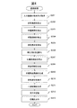
図5は、入力画像500の一例を示す模式図である。 FIG. 5 is a schematic diagram showing an example of the input image 500.

図5に示すように、入力画像500には、住所、会社名、電話番号又は役職等の文字501と、印鑑502〜505とが写っている。なお、文字501は黒色を有し、印鑑502〜505は赤色を有している。印鑑502〜505の内、印鑑503〜505は文字501と重なっていないが、印鑑502は文字501と重なっている。そのため、文字501と印鑑502が重なっている領域では、黒色と赤色が重なっている。 As shown in FIG. 5, the input image 500 shows characters 501 such as an address, a company name, a telephone number, or a job title, and stamps 502 to 505. The characters 501 have a black color, and the seals 502 to 505 have a red color. Of the seals 502 to 505, the seals 503 to 505 do not overlap with the character 501, but the seal 502 overlaps with the character 501. Therefore, in the area where the character 501 and the seal 502 overlap, black and red overlap.

次に、検出部222は、入力画像内の画素毎に赤色強度を算出する(ステップS202)。まず、検出部222は、入力画像内の各画素のRGB(赤色、緑色、青色)値をHSL(色相、彩度、輝度)値に変換する。次に、検出部222は、色相値が第1閾値(例えば30)未満である画素と、色相値が第2閾値(例えば330)より大きい画素(即ち、オレンジ色から赤紫色を有する画素)を抽出する。次に、検出部222は、抽出した各画素について、以下の式(1)に従って、各画素のRGB値から赤色強度を算出する。

Figure 0006970835
式(1)で示される赤色強度は、R値からG値を減算した値と、R値からB値を減算した値との合計値であり、各画素の赤色成分の強さを示す。Next, the detection unit 222 calculates the red intensity for each pixel in the input image (step S202). First, the detection unit 222 converts the RGB (red, green, blue) value of each pixel in the input image into the HSL (hue, saturation, luminance) value. Next, the detection unit 222 detects pixels having a hue value less than the first threshold value (for example, 30) and pixels having a hue value larger than the second threshold value (for example, 330) (that is, pixels having orange to magenta). Extract. Next, the detection unit 222 calculates the red intensity from the RGB values of each pixel according to the following formula (1) for each extracted pixel.
Figure 0006970835
The red intensity represented by the equation (1) is the total value of the value obtained by subtracting the G value from the R value and the value obtained by subtracting the B value from the R value, and indicates the intensity of the red component of each pixel.

なお、検出部222は、抽出した各画素について、以下の式(2)のように、各画素のS(彩度)値を赤色強度として使用してもよい。

Figure 0006970835
ここで、MAX値は各画素のR値、G値、B値の内の最大値であり、MIN値は各画素のR値、G値、B値の内の最小値である。The detection unit 222 may use the S (saturation) value of each pixel as the red intensity for each extracted pixel as in the following equation (2).
Figure 0006970835
Here, the MAX value is the maximum value among the R value, G value, and B value of each pixel, and the MIN value is the minimum value among the R value, G value, and B value of each pixel.

次に、検出部222は、算出した赤色強度に基づいて印鑑画素を抽出する(ステップS203)。検出部222は、算出した赤色強度が第3閾値(例えば32)以上である画素を印鑑画素に決定し、赤色強度が第3閾値未満である画素を非印鑑画素に決定する。 Next, the detection unit 222 extracts the stamp pixel based on the calculated red intensity (step S203). The detection unit 222 determines the pixel whose red intensity is equal to or higher than the third threshold value (for example, 32) as the stamp pixel, and determines the pixel whose red intensity is less than the third threshold value as the non-seal pixel.

図6は、印鑑画素について説明するための模式図である。 FIG. 6 is a schematic diagram for explaining the stamp pixel.

図6に示す画像600では、図5に示した入力画像500から抽出された印鑑画素602〜605が白色で示され、非印鑑画素601が黒色で示されている。図6に示すように、入力画像500において印鑑502〜505が写っている領域、即ち赤色を有する領域に対応する画素は印鑑画素602〜605として抽出され、他の画素は非印鑑画素601として抽出される。但し、入力画像500において文字501と印鑑502が重なっている領域、即ち黒色及び赤色を有する領域に対応する画素は、黒色と赤色の強さのバランスに応じて、一部は非印鑑画素601として抽出され、一部は印鑑画素602として抽出される。 In the image 600 shown in FIG. 6, the stamp pixels 602 to 605 extracted from the input image 500 shown in FIG. 5 are shown in white, and the non-stamp pixels 601 are shown in black. As shown in FIG. 6, in the input image 500, the pixel corresponding to the region in which the seal stamps 502 to 505 appears, that is, the region having red color is extracted as the seal stamp pixel 602 to 605, and the other pixels are extracted as the non-seal stamp pixel 601. Will be done. However, in the input image 500, the pixels corresponding to the region where the character 501 and the stamp 502 overlap, that is, the region having black and red, are partially designated as non-stamp pixels 601 depending on the balance of the intensity of black and red. It is extracted, and a part of it is extracted as a seal pixel 602.

次に、検出部222は、入力画像内で、抽出した印鑑画素が連結する領域を含む領域を、印鑑が含まれる印鑑領域、即ち印鑑に対応する印鑑領域として検出する(ステップS204)。検出部222は、相互に隣接する印鑑画素で囲まれる領域をラベリングにより一つのグループとしてまとめて印鑑領域とする。即ち、印鑑領域には、印鑑の外枠の内部領域が含まれる。なお、検出部222は、各グループの内、サイズ(面積)が所定範囲内であるグループのみを印鑑領域として検出してもよい。所定範囲は、一般的な印鑑が取り得る範囲に予め設定される。また、検出部222は、各グループの内、所定形状を有するグループのみを印鑑領域として検出してもよい。所定形状は、丸、四角等、一般的な印鑑が取り得る形状に予め設定される。例えば、検出部222は、各グループと所定形状との正規化相互相関値を算出し、算出した正規化相互相関値が所定値以上である場合に限り、そのグループを印鑑領域として検出する。また、検出部222は、各グループの外接矩形を印鑑領域として検出してもよい。 Next, the detection unit 222 detects the region including the region to which the extracted stamp pixels are connected in the input image as the stamp region including the stamp, that is, the stamp region corresponding to the stamp (step S204). The detection unit 222 groups the regions surrounded by the stamp pixels adjacent to each other into one group by labeling to form a stamp region. That is, the stamp area includes the inner area of the outer frame of the stamp. In addition, the detection unit 222 may detect only the group whose size (area) is within a predetermined range among the groups as the stamp area. The predetermined range is preset to a range that can be taken by a general seal. Further, the detection unit 222 may detect only the group having a predetermined shape among the groups as the stamp region. The predetermined shape is preset to a shape that can be taken by a general stamp, such as a circle or a square. For example, the detection unit 222 calculates a normalized cross-correlation value between each group and a predetermined shape, and detects the group as a stamp region only when the calculated normalized cross-correlation value is equal to or greater than a predetermined value. Further, the detection unit 222 may detect the circumscribed rectangle of each group as the stamp area.

図6に示す例では、印鑑画素602〜605の外接矩形612〜615が印鑑領域として検出されている。 In the example shown in FIG. 6, the circumscribed rectangles 612 to 615 of the stamp pixels 602 to 605 are detected as the stamp region.

次に、算出部223は、印鑑領域内の画素毎に、赤色割合を算出する(ステップS205)。算出部223は、各画素について、以下の式(3)に従って、各画素の赤色強度に基づいて、各画素の赤色割合を算出する。

Figure 0006970835
ここで、αは係数(例えば96)であり、赤色強度の値域幅に基づいて、予め設定される。また、βはオフセット値(例えば32)であり、赤色強度の値域に基づいて、予め設定される。赤色割合は、0以上であり且つ1以下である範囲内に設定される。即ち、式(3)により算出された値が0以下である場合、赤色割合は0に補正され、式(3)により算出された値が1以上である場合、赤色割合は1に補正される。式(3)で示される赤色割合は、各画素に含まれる各色成分の内の赤色成分の割合を示し、各画素に含まれる赤色成分が大きい程大きい値を有する。このように、算出部223は、各画素のR値、G値及びB値の内の少なくとも二つの色値の関係に基づいて、各画素の赤色割合を算出する。Next, the calculation unit 223 calculates the red ratio for each pixel in the stamp region (step S205). For each pixel, the calculation unit 223 calculates the red ratio of each pixel based on the red intensity of each pixel according to the following formula (3).
Figure 0006970835
Here, α is a coefficient (for example, 96) and is preset based on the range width of the red intensity. Further, β is an offset value (for example, 32) and is preset based on the range of red intensity. The red color ratio is set within the range of 0 or more and 1 or less. That is, when the value calculated by the formula (3) is 0 or less, the red ratio is corrected to 0, and when the value calculated by the formula (3) is 1 or more, the red ratio is corrected to 1. .. The red ratio represented by the formula (3) indicates the ratio of the red component among the color components contained in each pixel, and the larger the red component contained in each pixel, the larger the value. In this way, the calculation unit 223 calculates the red ratio of each pixel based on the relationship of at least two color values among the R value, G value, and B value of each pixel.

次に、算出部223は、印鑑領域内の画素毎に、明るさ割合を算出する(ステップS206)。まず、算出部223は、各画素の明るさを、以下の式(4)に従って、各画素のR値、G値及びB値に基づいて算出する。

Figure 0006970835
式(4)で示される明るさは、RGB座標系で示される各画素の原点(黒)からの距離を示す。Next, the calculation unit 223 calculates the brightness ratio for each pixel in the stamp area (step S206). First, the calculation unit 223 calculates the brightness of each pixel based on the R value, G value, and B value of each pixel according to the following equation (4).
Figure 0006970835
The brightness represented by the equation (4) indicates the distance from the origin (black) of each pixel represented by the RGB coordinate system.

なお、各画素の明るさは、以下の式(5)に従って算出されてもよい。

Figure 0006970835
この場合、算出部223は、簡易的に明るさを算出することができ、算出時間を短縮することができる。また、以下の式(6)のように、各画素の明るさとして、各画素のYUVフォーマットにおける輝度値が使用されてもよい。
Figure 0006970835
または、以下の式(7)のように、各画素の明るさとして、各画素のHSLフォーマットにおける輝度値が使用されてもよい。
Figure 0006970835
このように、各画素の明るさは、各画素の輝度値又はR値、G値及びB値に基づいて算出される。The brightness of each pixel may be calculated according to the following equation (5).
Figure 0006970835
In this case, the calculation unit 223 can easily calculate the brightness and shorten the calculation time. Further, as the brightness of each pixel, the luminance value in the YUV format of each pixel may be used as in the following equation (6).
Figure 0006970835
Alternatively, as in the following equation (7), the luminance value in the HSL format of each pixel may be used as the brightness of each pixel.
Figure 0006970835
In this way, the brightness of each pixel is calculated based on the luminance value or the R value, the G value, and the B value of each pixel.

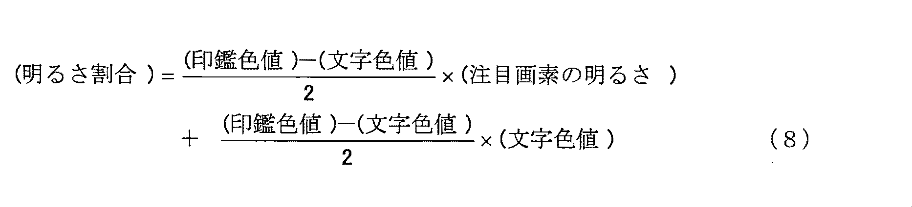
次に、算出部223は、印鑑領域内で印鑑を表す印鑑色値を算出する。算出部223は、印鑑領域内の印鑑画素の内、赤色強度が高い順から50%の印鑑画素の明るさの平均値を印鑑色値として算出する。また、算出部223は、印鑑領域内で文字を表す文字色値を算出する。算出部223は、印鑑領域内の画素の内、明るさが低い順(黒色に近い順)から1%の画素の明るさの平均値を文字色値として算出する。なお、印鑑色値又は文字色値として、各画素の明るさの中央値等、平均値以外の統計値が用いられてもよい。算出部223は、各画素について、以下の式(8)に従って、算出した印鑑色値及び文字色値と、各画素の明るさとに基づいて、各画素の明るさ割合を算出する。

Figure 0006970835
式(8)で示される明るさ割合は、印鑑領域内で算出された印鑑色値及び文字色値を考慮して算出される、各画素の明るさの割合を示し、各画素の明るさが大きい程大きい値を有する。Next, the calculation unit 223 calculates a stamp color value representing a stamp in the stamp area. The calculation unit 223 calculates the average value of the brightness of the stamp pixels of 50% from the stamp pixels in the stamp region in descending order of red intensity as the stamp color value. Further, the calculation unit 223 calculates a character color value representing a character in the stamp area. The calculation unit 223 calculates the average value of the brightness of 1% of the pixels in the stamp region from the lowest brightness (order closer to black) as the character color value. As the stamp color value or the character color value, a statistical value other than the average value such as the median brightness of each pixel may be used. The calculation unit 223 calculates the brightness ratio of each pixel for each pixel based on the calculated stamp color value and character color value and the brightness of each pixel according to the following formula (8).
Figure 0006970835
The brightness ratio represented by the formula (8) indicates the ratio of the brightness of each pixel calculated in consideration of the stamp color value and the character color value calculated in the stamp area, and the brightness of each pixel is The larger the value, the larger the value.

次に、算出部223は、印鑑領域内の画素毎に、算出した赤色割合及び明るさ割合に基づいて、印鑑色割合を算出する(ステップS207)。算出部223は、以下の式(9)に従って、各画素の赤色割合と各画素の明るさ割合の乗算値を、各画素の印鑑色割合として算出する。

Figure 0006970835
なお、算出部223は、各画素の赤色割合と各画素の明るさ割合の平均値を、各画素の印鑑色割合として算出してもよい。Next, the calculation unit 223 calculates the stamp color ratio for each pixel in the stamp region based on the calculated red color ratio and brightness ratio (step S207). The calculation unit 223 calculates the product of the red ratio of each pixel and the brightness ratio of each pixel as the stamp color ratio of each pixel according to the following equation (9).
Figure 0006970835
The calculation unit 223 may calculate the average value of the red color ratio of each pixel and the brightness ratio of each pixel as the stamp color ratio of each pixel.

次に、背景情報生成部224は、背景情報を生成する(ステップS208)。背景情報生成部224は、入力画像内の全ての画素について背景情報を生成する。まず、背景情報生成部224は、入力画像の各画素に対して、平均フィルタ又はガウシアンフィルタ等の平滑フィルタを適用してノイズを除去する。次に、背景情報生成部224は、ノイズを除去した入力画像に対して白色成分を膨張させた膨張画像を生成し、膨張画像内の各画素の画素値(R値、G値、B値)を、対応する入力画像内の各画素の背景情報として決定する。即ち、入力画像内の注目画素に対応する背景情報は、注目画素の周辺画素の中で輝度が最も高い画素の画素値(R値、G値、B値)に設定される。 Next, the background information generation unit 224 generates background information (step S208). The background information generation unit 224 generates background information for all the pixels in the input image. First, the background information generation unit 224 removes noise by applying a smoothing filter such as an average filter or a Gaussian filter to each pixel of the input image. Next, the background information generation unit 224 generates an expanded image in which the white component is expanded with respect to the input image from which noise has been removed, and the pixel values (R value, G value, B value) of each pixel in the expanded image. Is determined as the background information of each pixel in the corresponding input image. That is, the background information corresponding to the pixel of interest in the input image is set to the pixel value (R value, G value, B value) of the pixel having the highest brightness among the peripheral pixels of the pixel of interest.

図7A及び図7Bは、背景情報について説明するための模式図である。 7A and 7B are schematic views for explaining background information.

図7Aに示す画像700及び図7Bに示す画像710は、図5に示した入力画像500から生成された背景情報を画素値とする画素からなる背景画像である。画像700は、注目画素を中心に一辺が5画素である矩形範囲を周辺画素として生成された背景画像であり、画像710は、注目画素を中心に一辺が15画素である矩形範囲を周辺画素として生成された背景画像である。背景画像700には、文字701、印鑑702〜705及び罫線706の成分が強く残っている。一方、背景画像710では、文字711、印鑑712〜715及び罫線716の成分は十分に小さくなり、文字711、印鑑712〜715及び罫線716は背景に溶け込んでいる。このように、例えば注目画素を中心に一辺が15画素である矩形範囲を周辺画素として設定することにより、背景情報生成部224は、文字、印鑑及び罫線の成分が除去された背景情報を生成することができる。 The image 700 shown in FIG. 7A and the image 710 shown in FIG. 7B are background images composed of pixels having background information generated from the input image 500 shown in FIG. 5 as pixel values. The image 700 is a background image generated with a rectangular range having 5 pixels on each side centered on the pixel of interest as peripheral pixels, and the image 710 has a rectangular range having 15 pixels on each side centered on the pixel of interest as peripheral pixels. It is a generated background image. In the background image 700, the components of the characters 701, the seals 702 to 705, and the ruled lines 706 remain strongly. On the other hand, in the background image 710, the components of the characters 711, the seals 712-715 and the ruled lines 716 are sufficiently small, and the characters 711, the seals 712-715 and the ruled lines 716 are blended into the background. In this way, for example, by setting a rectangular range having 15 pixels on each side centered on the pixel of interest as peripheral pixels, the background information generation unit 224 generates background information from which the components of characters, stamps, and ruled lines have been removed. be able to.

次に、印鑑除去画像生成部225は、入力画像から印鑑成分を除去した印鑑除去画像を生成する(ステップS209)。印鑑除去画像生成部225は、印鑑色割合に基づいて、印鑑領域内の各画素と、各画素に対応する背景情報とを合成することにより、印鑑除去画像を生成する。印鑑除去画像生成部225は、各画素のR値、G値、B値を、それぞれ、以下の式(10)に従って算出されるDr、Dg、Dbとする印鑑除去画像を生成する。

Figure 0006970835
ここで、Sr、Sg、Sbはそれぞれ各画素に対応する入力画像内の画素のR値、G値、B値であり、Br、Bg、Bbはそれぞれ各画素に対応する背景情報のR値、G値、B値である。即ち、印鑑除去画像内の各画素のRGB値は、各画素の印鑑色割合が大きい程、背景情報のRGB値に近く、各画素の印鑑色割合が小さい程、入力画像内の対応する画素のRGB値に近い。Next, the seal stamp removal image generation unit 225 generates a seal stamp removal image from which the seal stamp component is removed from the input image (step S209). The stamp removal image generation unit 225 generates a stamp removal image by synthesizing each pixel in the stamp region and background information corresponding to each pixel based on the stamp color ratio. The seal removal image generation unit 225 generates a seal removal image in which the R value, G value, and B value of each pixel are D r , D g , and D b calculated according to the following equation (10), respectively.
Figure 0006970835
Here, S r , S g , and S b are R values, G values, and B values of the pixels in the input image corresponding to each pixel, and B r , B g , and B b correspond to each pixel, respectively. The R value, G value, and B value of the background information. That is, the RGB value of each pixel in the stamp-removed image is closer to the RGB value of the background information as the stamp color ratio of each pixel is larger, and the smaller the stamp color ratio of each pixel is, the corresponding pixel in the input image. Close to RGB values.

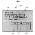
図8Aは、印鑑除去画像800の一例を示す模式図である。 FIG. 8A is a schematic diagram showing an example of the stamp removal image 800.

図8Aに示す印鑑除去画像800は、図5に示した入力画像500から生成された印鑑除去画像である。図8Aに示すように、印鑑除去画像800では、文字801の成分は残りつつ、印鑑802〜805の成分は良好に除去されている。特に、印鑑除去画像800では、入力画像500において印鑑502と重なっていた文字501の成分が、印鑑502とともに除去されることなく残っている。 The stamp removal image 800 shown in FIG. 8A is a stamp removal image generated from the input image 500 shown in FIG. As shown in FIG. 8A, in the stamp removal image 800, the components of the characters 801 remain, but the components of the stamps 802 to 805 are satisfactorily removed. In particular, in the stamp removal image 800, the component of the character 501 that overlaps with the stamp 502 in the input image 500 remains without being removed together with the stamp 502.

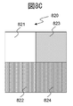
図8B及び図8Cは、印鑑除去画像について説明するための模式図である。 8B and 8C are schematic views for explaining the stamp-removed image.

図8Bは、入力画像810の印鑑領域の一部を示し、領域811は白色の背景を示し、領域812は黒色の文字を示し、領域813は背景上に押された赤色の印鑑を示し、領域814は文字上に押された印鑑を示している。この場合、領域813の赤色割合は、領域811、812の赤色割合より大きい。一方、領域814では黒色の文字の影響により赤色成分が小さいため、領域814の赤色割合は、領域811、812の赤色割合より大きいものの、領域813の赤色割合と比較すると小さい。また、領域811、813の明るさ割合は、それぞれ領域812、814の明るさ割合より大きい。 FIG. 8B shows a part of the stamp region of the input image 810, the region 811 shows a white background, the region 812 shows black characters, and the region 813 shows a red stamp stamped on the background. 814 indicates a stamp stamped on the letters. In this case, the red proportion of the region 813 is larger than the red proportion of the regions 811 and 812. On the other hand, since the red component is small in the region 814 due to the influence of the black characters, the red ratio of the region 814 is larger than the red ratio of the regions 811 and 812, but smaller than the red ratio of the region 813. Further, the brightness ratio of the regions 811 and 813 is larger than the brightness ratio of the regions 812 and 814, respectively.

図8Cは、入力画像810から生成された印鑑除去画像820の印鑑領域の一部を示し、領域821、822、823、824はそれぞれ領域811、812、813、814に対応している。上記したように、印鑑除去画像生成部225は、赤色割合及び明るさ割合に基づいて算出された印鑑色割合に基づいて、入力画像810内の各画素のRGB値と背景情報のRGB値とを合成する。領域811の背景情報のRGB値は領域811の各画素のRGB値とほぼ同じであるため、印鑑除去画像820の領域821のRGB値は、入力画像810の領域811のRGB値と同様になる。また、領域812では、赤色割合及び明るさ割合が小さいため、印鑑色割合が小さくなり、印鑑除去画像820の領域822のRGB値は、入力画像810の領域812のRGB値と同様になる。 FIG. 8C shows a part of the stamp region of the stamp removal image 820 generated from the input image 810, and the regions 821, 822, 823, and 824 correspond to the regions 811, 812, 813, and 814, respectively. As described above, the stamp removal image generation unit 225 determines the RGB value of each pixel in the input image 810 and the RGB value of the background information based on the stamp color ratio calculated based on the red color ratio and the brightness ratio. Synthesize. Since the RGB value of the background information of the region 811 is substantially the same as the RGB value of each pixel of the region 811, the RGB value of the region 821 of the stamp removal image 820 is the same as the RGB value of the region 811 of the input image 810. Further, in the region 812, since the red color ratio and the brightness ratio are small, the seal color ratio becomes small, and the RGB value of the region 822 of the seal stamp removed image 820 becomes the same as the RGB value of the region 812 of the input image 810.

一方、領域813では、赤色割合及び明るさ割合が大きいため、印鑑色割合が大きく、印鑑除去画像820の領域823のRGB値は、入力画像810の領域813のRGB値より背景情報のRBG値に近い(領域823は背景に近い)。また、領域814では、赤色割合及び明るさ割合が領域813の赤色割合及び明るさ割合より小さいため、印鑑色割合が領域813の印鑑色割合より小さい。そのため、印鑑除去画像820の領域824のRGB値は、背景情報のRGB値より入力画像810の領域814のRGB値に近い(領域824は領域814に近い)。 On the other hand, in the region 813, since the red color ratio and the brightness ratio are large, the stamp color ratio is large, and the RGB value of the region 823 of the stamp removed image 820 is the RBG value of the background information rather than the RGB value of the region 813 of the input image 810. Close (region 823 is close to the background). Further, in the region 814, the red color ratio and the brightness ratio are smaller than the red color ratio and the brightness ratio of the region 813, so that the stamp color ratio is smaller than the stamp color ratio of the region 813. Therefore, the RGB value of the region 824 of the seal stamp removed image 820 is closer to the RGB value of the region 814 of the input image 810 than the RGB value of the background information (the region 824 is closer to the region 814).

また、印鑑除去画像生成部225は、入力画像810内の画素のRGB値を、固定のRGB値(例えば白色のRGB値)でなく、背景情報のRGB値と合成する。これにより、合成後の領域823及び領域824は、周辺領域と近い色合いを有するため、印鑑除去画像において印鑑が除去された領域に不自然な色が発生することが抑制される。 Further, the stamp removal image generation unit 225 combines the RGB values of the pixels in the input image 810 with the RGB values of the background information instead of the fixed RGB values (for example, the RGB values of white). As a result, since the combined region 823 and 824 have a hue close to that of the peripheral region, it is possible to suppress the generation of unnatural colors in the region from which the stamp has been removed in the stamp-removed image.

次に、二値画像生成部226は、生成した印鑑除去画像に対して、赤色成分を除去するドロップアウト処理を実行することにより、赤色成分除去画像を生成する(ステップS210)。二値画像生成部226は、印鑑除去画像内の各画素のRGBの各色の値をR値とし、赤色成分除去画像として生成する。 Next, the binary image generation unit 226 generates a red component-removed image by executing a dropout process for removing the red component from the generated stamp-removed image (step S210). The binary image generation unit 226 sets the value of each color of RGB of each pixel in the stamp-removed image as an R value, and generates the image as a red component-removed image.

図9Aは、赤色成分除去画像900の一例を示す模式図である。 FIG. 9A is a schematic diagram showing an example of the red component removal image 900.

図9Aに示す赤色成分除去画像900は、図5に示した入力画像500から生成された赤色成分除去画像である。図8Aに示す印鑑除去画像800では、印鑑802〜805の成分は良好に除去されているが、印鑑802〜805の領域はわずかに赤味がかっている。一方、図9Aに示す赤色成分除去画像900では、文字901及び印鑑902〜905を含む全領域が背景色で表され、印鑑902〜905の成分は印鑑除去画像800よりさらに除去されている。 The red component removal image 900 shown in FIG. 9A is a red component removal image generated from the input image 500 shown in FIG. In the stamp removal image 800 shown in FIG. 8A, the components of the stamps 802 to 805 are satisfactorily removed, but the region of the stamps 802 to 805 is slightly reddish. On the other hand, in the red component-removed image 900 shown in FIG. 9A, the entire region including the characters 901 and the stamps 902 to 905 is represented by the background color, and the components of the stamps 902 to 905 are further removed from the stamp-removed image 800.

図9Bは、赤色成分除去画像について説明するための模式図である。 FIG. 9B is a schematic diagram for explaining a red component-removed image.

図9Bは、図8Cの印鑑除去画像820から生成された赤色成分除去画像910の印鑑領域の一部を示し、領域911、912、913、914は、それぞれ領域821、822、823、824に対応している。印鑑除去画像820の領域821は白色を有しており、白色ではR値、G値及びB値が全て大きいため、領域911の輝度値は大きい。一方、印鑑除去画像820の領域822は黒色を有しており、黒色ではR値、G値及びB値が全て小さいため、領域912の輝度値は小さい。 FIG. 9B shows a part of the stamp region of the red component removal image 910 generated from the stamp removal image 820 of FIG. 8C, and the regions 911, 912, 913, and 914 correspond to the regions 821, 822, 823, and 824, respectively. doing. The region 821 of the seal stamp removed image 820 has white color, and since the R value, the G value, and the B value are all large in the white color, the luminance value of the region 911 is large. On the other hand, the region 822 of the seal stamp removed image 820 has a black color, and since the R value, the G value, and the B value are all small in the black color, the luminance value of the region 912 is small.

また、印鑑除去画像820の領域823は、入力画像810において赤色を有する領域813と、白色を有する背景情報とを合成して生成されている。したがって、領域823のR値は大きいため、領域913の輝度値は大きい。一方、印鑑除去画像820の領域824は、入力画像810において赤味がかった黒色を有する領域813に、白色を有する背景情報がわずかに合成されて生成されている。そのため、領域813には赤色成分がわずかに含まれており、領域913の輝度値はわずかに高い値(白色と黒色の中間の値)となる。 Further, the region 823 of the stamp removal image 820 is generated by synthesizing the region 813 having a red color and the background information having a white color in the input image 810. Therefore, since the R value of the region 823 is large, the luminance value of the region 913 is large. On the other hand, the region 824 of the stamp removal image 820 is generated by slightly synthesizing the background information having white color with the region 813 having reddish black color in the input image 810. Therefore, the region 813 contains a small amount of a red component, and the luminance value of the region 913 is a slightly high value (a value between white and black).

次に、二値画像生成部226は、生成した赤色成分除去画像に対して、二値化処理を実行することにより、二値画像を生成する(ステップS211)。二値画像生成部226は、赤色成分除去画像内で輝度値が第4閾値以上である画素を白色画素とし、輝度値が第4閾値未満である画素を黒色画素とした画像を二値画像として生成する。第4閾値は、事前の実験により、赤色成分除去画像において文字上に押された印鑑に対応する領域(領域914)の輝度値より大きくなるように設定される。これにより、二値画像では、入力画像内の文字に対応する画素が黒色画素となり、入力画像内の他の画素に対応する画素が白色画素となる。 Next, the binary image generation unit 226 generates a binary image by executing a binarization process on the generated red component-removed image (step S211). The binary image generation unit 226 uses a pixel having a luminance value of less than the fourth threshold as a white pixel and a pixel having a luminance value less than the fourth threshold as a black pixel in the red component-removed image as a binary image. Generate. The fourth threshold value is set to be larger than the luminance value of the region (region 914) corresponding to the stamp stamped on the characters in the red component-removed image by a prior experiment. As a result, in the binary image, the pixel corresponding to the character in the input image becomes a black pixel, and the pixel corresponding to another pixel in the input image becomes a white pixel.

次に、文字認識部227は、公知のOCR(Optical Character Recognition)技術を利用して、生成された二値画像から文字を検出する(ステップS212)。 Next, the character recognition unit 227 detects a character from the generated binary image by using a known OCR (Optical Character Recognition) technique (step S212).

次に、出力制御部228は、検出された文字を表示装置203に表示し(ステップS213)、一連のステップを終了する。なお、出力制御部228は、検出された文字に代えて又は加えて、印鑑除去画像、赤色成分除去画像又は二値画像を表示装置203に表示してもよい。また、出力制御部228は、検出された文字、印鑑除去画像、赤色成分除去画像又は二値画像を不図示の通信装置を介して不図示のサーバ等に送信してもよい。このように、出力制御部228は、印鑑除去画像又は印鑑除去画像を用いて生成した情報を出力する。 Next, the output control unit 228 displays the detected characters on the display device 203 (step S213), and ends a series of steps. The output control unit 228 may display the stamp removal image, the red component removal image, or the binary image on the display device 203 in place of or in addition to the detected characters. Further, the output control unit 228 may transmit the detected character, the seal stamp removal image, the red component removal image, or the binary image to a server (not shown) or the like via a communication device (not shown). In this way, the output control unit 228 outputs the stamp removal image or the information generated by using the stamp removal image.

なお、算出部223は、印鑑領域内の画素毎に、赤色割合及び明るさ割合の内の何れか一方の割合を算出し、算出した割合に基づいて印鑑色割合を算出してもよい。その場合、算出部223は、ステップS205又はS206の処理の内の一方を省略する。算出部223は、ステップS207において、赤色割合又は明るさ割合の内の一方の割合、又は、その割合と所定係数の乗算値もしくはその割合と所定オフセットの加算値を印鑑色割合として算出する。情報処理装置200は、赤色割合及び明るさ割合の両方に基づいて印鑑色割合を算出する場合、より高精度に文字成分を残しつつ印鑑成分を除去することが可能となる。一方、情報処理装置200は、赤色割合及び明るさ割合の何れか一方に基づいて印鑑色割合を算出する場合、より短時間に印鑑除去画像を生成することが可能となり、画像生成処理の処理負荷を低減することが可能となる。 The calculation unit 223 may calculate the ratio of either the red color ratio or the brightness ratio for each pixel in the seal stamp region, and calculate the seal stamp color ratio based on the calculated ratio. In that case, the calculation unit 223 omits one of the processes of steps S205 or S206. In step S207, the calculation unit 223 calculates the ratio of one of the red color ratio and the brightness ratio, the multiplication value of the ratio and the predetermined coefficient, or the addition value of the ratio and the predetermined offset as the stamp color ratio. When the information processing apparatus 200 calculates the stamp color ratio based on both the red color ratio and the brightness ratio, it is possible to remove the stamp component while leaving the character component with higher accuracy. On the other hand, when the information processing apparatus 200 calculates the seal stamp color ratio based on either the red color ratio or the brightness ratio, it is possible to generate the seal stamp removal image in a shorter time, and the processing load of the image generation process. Can be reduced.

また、背景情報生成部224は、印鑑領域において印鑑除去画像生成部225が合成する画素についてのみ背景情報を生成してもよい。その場合、背景情報生成部224は、ステップS208において、入力画像内の全ての画素について背景情報を生成するのでなく、印鑑領域内の画素についてのみ背景情報を生成する。または、背景情報生成部224は、印鑑色割合が0より大きい画素についてのみ背景情報を生成してもよい。これにより、情報処理装置200は、より短時間に印鑑除去画像を生成することが可能となり、画像生成処理の処理負荷を低減することが可能となる。 Further, the background information generation unit 224 may generate background information only for the pixels synthesized by the seal stamp removal image generation unit 225 in the seal stamp region. In that case, in step S208, the background information generation unit 224 does not generate background information for all the pixels in the input image, but generates background information only for the pixels in the stamp area. Alternatively, the background information generation unit 224 may generate background information only for pixels having a stamp color ratio larger than 0. As a result, the information processing apparatus 200 can generate a stamp-removed image in a shorter time, and can reduce the processing load of the image generation processing.

また、二値画像生成部226は、ステップS210の処理を省略し、赤色成分除去画像を生成せずに印鑑除去画像から二値画像を生成してもよい。 Further, the binary image generation unit 226 may omit the process of step S210 and generate a binary image from the stamp-removed image without generating the red component-removed image.

以上詳述したように、図4に示したフローチャートに従って動作することによって、情報処理装置200は、入力画像において、各画素の印鑑色割合に基づいて、各画素と各画素に対応する背景情報とを合成することにより、印鑑成分を除去する。これにより、情報処理装置200は、印鑑が含まれる入力画像から印鑑成分をより精度良く除去することが可能となった。 As described in detail above, by operating according to the flowchart shown in FIG. 4, the information processing apparatus 200 provides the input image with the background information corresponding to each pixel and each pixel based on the stamp color ratio of each pixel. The seal component is removed by synthesizing. As a result, the information processing apparatus 200 can more accurately remove the stamp component from the input image including the stamp.

例えば、入力画像に対して直接、各画素の輝度値に基づいて二値化処理が実行されると、赤色の印鑑が写っている領域も黒色の文字が写っている領域と同様に黒色画素となる可能性がある。一方、入力画像に対して直接、赤色成分を除去するドロップアウト処理が実行されると、文字と印鑑が重なっている領域の赤色成分が強い場合に、その領域が文字として残らない可能性がある。情報処理装置200は、各画素の明るさ割合を考慮して印鑑成分を除去することにより、黒色の文字に印鑑が重なっている領域を印鑑として除去せずに文字として残すことが可能となる。 For example, when the binarization process is directly executed on the input image based on the brightness value of each pixel, the area where the red seal is shown becomes the black pixel as well as the area where the black characters are shown. There is a possibility of becoming. On the other hand, if the dropout process for removing the red component is executed directly on the input image, if the red component in the area where the characters and the seal overlap is strong, that area may not remain as characters. .. By removing the stamp component in consideration of the brightness ratio of each pixel, the information processing apparatus 200 can leave the region where the stamp overlaps with the black character as a character without removing it as a stamp.

また、入力画像に対して直接、赤色成分を除去するドロップアウト処理が実行されると、印鑑の赤色成分が背景の赤色成分より強い場合に、印鑑が写っていた領域が背景より明るくなり、目立ってしまう可能性がある。情報処理装置200は、入力画像内の印鑑に対応する画素を背景情報と合成することにより、印鑑成分を背景成分に近づけて背景に埋めることが可能となり、印鑑成分を良好に除去することが可能となる。 In addition, when the dropout process for removing the red component is executed directly on the input image, when the red component of the stamp is stronger than the red component of the background, the area where the stamp is reflected becomes brighter than the background and stands out. There is a possibility that it will end up. By synthesizing the pixels corresponding to the seal stamp in the input image with the background information, the information processing apparatus 200 can bring the seal stamp component closer to the background component and bury it in the background, and can satisfactorily remove the seal stamp component. It becomes.

図10は、他の実施形態に係る情報処理装置における処理装置230の概略構成を示すブロック図である。 FIG. 10 is a block diagram showing a schematic configuration of a processing device 230 in the information processing device according to another embodiment.

処理装置230は、CPU220の代わりに、認識処理を実行する。処理装置230は、取得回路231、検出回路232、算出回路233、背景情報生成回路234、印鑑除去画像生成回路235、二値画像生成回路236、文字認識回路237及び出力制御回路238等を有する。 The processing device 230 executes the recognition process instead of the CPU 220. The processing device 230 includes an acquisition circuit 231, a detection circuit 232, a calculation circuit 233, a background information generation circuit 234, a stamp removal image generation circuit 235, a binary image generation circuit 236, a character recognition circuit 237, an output control circuit 238, and the like.

取得回路231は、取得部の一例であり、取得部221と同様の機能を有する。取得回路231は、入力画像を第2インタフェース装置201を介して画像読取装置100から取得し、第2記憶装置210に保存する。 The acquisition circuit 231 is an example of the acquisition unit, and has the same function as the acquisition unit 221. The acquisition circuit 231 acquires the input image from the image reading device 100 via the second interface device 201 and stores it in the second storage device 210.

検出回路232は、検出部の一例であり、検出部222と同様の機能を有する。検出回路232は、第2記憶装置210から入力画像を読み出し、入力画像内で印鑑に対応する印鑑領域を検出し、検出結果を第2記憶装置210に保存する。 The detection circuit 232 is an example of the detection unit, and has the same function as the detection unit 222. The detection circuit 232 reads an input image from the second storage device 210, detects a stamp area corresponding to the stamp in the input image, and stores the detection result in the second storage device 210.

算出回路233は、算出部の一例であり、算出部223と同様の機能を有する。算出回路233は、第2記憶装置210から入力画像及び印鑑領域の検出結果を読み出し、印鑑領域内の画素毎に印鑑色割合を算出し、第2記憶装置210に保存する。 The calculation circuit 233 is an example of the calculation unit, and has the same function as the calculation unit 223. The calculation circuit 233 reads the input image and the detection result of the stamp area from the second storage device 210, calculates the stamp color ratio for each pixel in the stamp area, and stores it in the second storage device 210.

背景情報生成回路234は、背景情報生成部の一例であり、背景情報生成部224と同様の機能を有する。背景情報生成回路234は、第2記憶装置210から入力画像を読み出し、入力画像内の各画素の背景情報を生成し、第2記憶装置210に保存する。 The background information generation circuit 234 is an example of the background information generation unit, and has the same function as the background information generation unit 224. The background information generation circuit 234 reads an input image from the second storage device 210, generates background information for each pixel in the input image, and stores the background information in the second storage device 210.

印鑑除去画像生成回路235は、印鑑除去画像生成部の一例であり、印鑑除去画像生成部225と同様の機能を有する。印鑑除去画像生成回路235は、第2記憶装置210から入力画像、印鑑領域の検出結果、印鑑色割合及び背景情報を読み出し、印鑑除去画像を生成し、第2記憶装置210に保存する。 The seal stamp removal image generation circuit 235 is an example of the seal stamp removal image generation unit, and has the same function as the seal stamp removal image generation unit 225. The seal stamp removal image generation circuit 235 reads the input image, the detection result of the seal stamp area, the seal stamp color ratio and the background information from the second storage device 210, generates the seal stamp removal image, and stores it in the second storage device 210.

二値画像生成回路236は、二値画像生成部の一例であり、二値画像生成部226と同様の機能を有する。二値画像生成回路236は、第2記憶装置210から印鑑除去画像を読み出し、印鑑除去画像から二値画像を生成し、第2記憶装置210に保存する。 The binary image generation circuit 236 is an example of the binary image generation unit, and has the same function as the binary image generation unit 226. The binary image generation circuit 236 reads the stamp-removed image from the second storage device 210, generates a binary image from the stamp-removed image, and stores the binary image in the second storage device 210.

文字認識回路237は、文字認識部の一例であり、文字認識部227と同様の機能を有する。文字認識回路237は、第2記憶装置210から二値画像を読み出し、二値画像から文字を検出し、検出結果を第2記憶装置210に保存する。 The character recognition circuit 237 is an example of the character recognition unit, and has the same function as the character recognition unit 227. The character recognition circuit 237 reads a binary image from the second storage device 210, detects characters from the binary image, and stores the detection result in the second storage device 210.

出力制御回路238は、出力制御部の一例であり、出力制御部228と同様の機能を有する。出力制御回路238は、第2記憶装置210から文字の検出結果、印鑑除去画像又は二値画像を読み出し、読み出した情報を表示装置203に出力する。 The output control circuit 238 is an example of the output control unit, and has the same function as the output control unit 228. The output control circuit 238 reads out the character detection result, the stamp removal image or the binary image from the second storage device 210, and outputs the read information to the display device 203.

以上詳述したように、情報処理装置は、処理装置230を用いる場合も、印鑑が含まれる入力画像から印鑑成分をより精度良く除去することが可能となった。 As described in detail above, the information processing apparatus can more accurately remove the stamp component from the input image including the stamp even when the processing device 230 is used.

以上、好適な実施形態について説明してきたが、実施形態はこれらに限定されない。例えば、画像読取装置100と情報処理装置200の機能分担は、図1に示す画像処理システム1の例に限られず、画像読取装置100及び情報処理装置200の各部を画像読取装置100と情報処理装置200の何れに配置するかは適宜変更可能である。または、画像読取装置100と情報処理装置200を一つの装置で構成してもよい。 Although the preferred embodiments have been described above, the embodiments are not limited thereto. For example, the division of functions between the image reading device 100 and the information processing device 200 is not limited to the example of the image processing system 1 shown in FIG. 1, and each part of the image reading device 100 and the information processing device 200 is divided into the image reading device 100 and the information processing device. Which of the 200 is arranged can be changed as appropriate. Alternatively, the image reading device 100 and the information processing device 200 may be configured by one device.

例えば、画像読取装置100の第1記憶装置110が、情報処理装置200の第2記憶装置210に記憶された各プログラムを記憶し、画像読取装置100の第1CPU120が、情報処理装置200の第2CPU120により実現される各部として動作してもよい。また、画像読取装置100が、情報処理装置200の処理装置230と同様の処理装置を有してもよい。 For example, the first storage device 110 of the image reading device 100 stores each program stored in the second storage device 210 of the information processing device 200, and the first CPU 120 of the image reading device 100 is the second CPU 120 of the information processing device 200. It may operate as each part realized by. Further, the image reading device 100 may have the same processing device as the processing device 230 of the information processing device 200.

その場合、画像読取装置100は表示装置203と同様の表示装置を有する。認識処理は画像読取装置100で実行されるため、ステップS102、S201の入力画像の送受信処理は省略される。ステップS202〜S213の各処理は、画像読取装置100の第1CPU120又は処理装置によって実行される。これらの処理の動作は、情報処理装置200の第2CPU220又は処理装置230によって実行される場合と同様である。 In that case, the image reading device 100 has a display device similar to the display device 203. Since the recognition process is executed by the image reading device 100, the transmission / reception processing of the input images in steps S102 and S201 is omitted. Each process of steps S202 to S213 is executed by the first CPU 120 of the image reading device 100 or the processing device. The operation of these processes is the same as that executed by the second CPU 220 of the information processing apparatus 200 or the processing apparatus 230.

また、画像処理システム1において、第1インタフェース装置101と第2インタフェース装置201は、インターネット、電話回線網(携帯端末回線網、一般電話回線網を含む)、イントラネット等のネットワークを介して接続してもよい。その場合、第1インタフェース装置101及び第2インタフェース装置201に、接続するネットワークの通信インタフェース回路を備える。また、その場合、クラウドコンピューティングの形態で画像処理のサービスを提供できるように、ネットワーク上に複数の情報処理装置を分散して配置し、各情報処理装置が協働して、認識処理等を分担するようにしてもよい。これにより、画像処理システム1は、複数の画像読取装置が読み取った入力画像について、効率よく認識処理を実行できる。 Further, in the image processing system 1, the first interface device 101 and the second interface device 201 are connected via a network such as the Internet, a telephone line network (including a mobile terminal line network and a general telephone line network), and an intranet. May be good. In that case, the first interface device 101 and the second interface device 201 are provided with a communication interface circuit of the network to be connected. In that case, a plurality of information processing devices are distributed and arranged on the network so that the image processing service can be provided in the form of cloud computing, and each information processing device cooperates to perform recognition processing and the like. You may share it. As a result, the image processing system 1 can efficiently perform recognition processing on the input images read by the plurality of image reading devices.

1 画像処理システム
200 情報処理装置
221 取得部
222 検出部
223 算出部
224 背景情報生成部
225 印鑑除去画像生成部
228 出力制御部
1 Image processing system 200 Information processing device 221 Acquisition unit 222 Detection unit 223 Calculation unit 224 Background information generation unit 225 Seal removal image generation unit 228 Output control unit

Claims (12)

入力画像を取得する取得部と、
前記入力画像内で印鑑に対応する印鑑領域を検出する検出部と、
前記印鑑領域内の画素毎に、印鑑色割合を算出する算出部と、
背景情報を生成する背景情報生成部と、
前記印鑑色割合に基づいて、前記印鑑領域内の各画素と、各画素に対応する前記背景情報とを合成することにより、前記入力画像から印鑑成分を除去した印鑑除去画像を生成する印鑑除去画像生成部と、
前記印鑑除去画像又は前記印鑑除去画像を用いて生成した情報を出力する出力部と、
を有することを特徴とする画像処理装置。
The acquisition unit that acquires the input image and
A detection unit that detects the stamp area corresponding to the stamp in the input image, and
A calculation unit that calculates the stamp color ratio for each pixel in the stamp area,
A background information generator that generates background information, and a background information generator
A stamp removal image that generates a stamp removal image in which the stamp component is removed from the input image by synthesizing each pixel in the stamp region and the background information corresponding to each pixel based on the stamp color ratio. The generator and
An output unit that outputs the stamp removal image or information generated by using the stamp removal image, and
An image processing apparatus characterized by having.
前記算出部は、前記印鑑領域内の画素毎に、赤色割合及び明るさ割合の内の何れか一方の割合を算出し、前記算出した割合に基づいて、前記印鑑色割合を算出する、請求項1に記載の画像処理装置。 The calculation unit calculates the ratio of either the red color ratio or the brightness ratio for each pixel in the seal stamp region, and calculates the seal stamp color ratio based on the calculated ratio. The image processing apparatus according to 1. 前記算出部は、前記印鑑領域内の画素毎に、赤色割合及び明るさ割合を算出し、前記算出した赤色割合及び明るさ割合に基づいて、前記印鑑色割合を算出する、請求項1に記載の画像処理装置。 The calculation unit calculates the red color ratio and the brightness ratio for each pixel in the seal stamp region, and calculates the seal color ratio based on the calculated red color ratio and the brightness ratio, according to claim 1. Image processing equipment. 前記入力画像は、カラー多値画像である、請求項1〜3の何れか一項に記載の画像処理装置。 The image processing apparatus according to any one of claims 1 to 3, wherein the input image is a color multi-valued image. 前記算出部は、各画素の赤色値、緑色値及び青色値の内の少なくとも二つの色値の関係に基づいて、各画素の赤色割合を算出する、請求項2〜4の何れか一項に記載の画像処理装置。 The calculation unit calculates the red ratio of each pixel based on the relationship of at least two color values among the red value, the green value and the blue value of each pixel, according to any one of claims 2 to 4. The image processing device described. 前記算出部は、前記印鑑領域内で印鑑色値及び文字色値を算出し、前記算出した印鑑色値及び文字色値と、各画素の輝度値又は赤色値、緑色値及び青色値とに基づいて、各画素の明るさ割合を算出する、請求項2〜5の何れか一項に記載の画像処理装置。 The calculation unit calculates the seal color value and the character color value in the seal area, and is based on the calculated seal color value and the character color value and the brightness value or the red value, the green value, and the blue value of each pixel. The image processing apparatus according to any one of claims 2 to 5, wherein the brightness ratio of each pixel is calculated. 前記検出部は、前記入力画像内の画素毎に赤色強度を算出し、前記算出した赤色強度に基づいて印鑑画素を抽出し、前記抽出した印鑑画素が連結する領域を含む領域を前記印鑑領域として検出する、請求項1〜6の何れか一項に記載の画像処理装置。 The detection unit calculates a red intensity for each pixel in the input image, extracts a stamp pixel based on the calculated red intensity, and uses a region including a region to which the extracted stamp pixels are connected as the stamp region. The image processing apparatus according to any one of claims 1 to 6 to be detected. 前記背景情報生成部は、前記入力画像内の全ての画素について前記背景情報を生成する、請求項1〜7の何れか一項に記載の画像処理装置。 The image processing apparatus according to any one of claims 1 to 7, wherein the background information generation unit generates the background information for all the pixels in the input image. 前記背景情報生成部は、前記印鑑領域において前記印鑑除去画像生成部が合成する画素について前記背景情報を生成する、請求項1〜7の何れか一項に記載の画像処理装置。 The image processing apparatus according to any one of claims 1 to 7, wherein the background information generation unit generates background information for pixels synthesized by the seal removal image generation unit in the seal area. 前記背景情報生成部は、注目画素に対応する前記背景情報を、前記注目画素の周辺画素の中で輝度が最も高い画素の画素値に設定する、請求項1〜9の何れか一項に記載の画像処理装置。 The background information generation unit according to any one of claims 1 to 9, wherein the background information corresponding to the pixel of interest is set to the pixel value of the pixel having the highest brightness among the peripheral pixels of the pixel of interest. Image processing equipment. 出力部を有する画像処理装置の制御方法であって、前記画像処理装置が、
入力画像を取得し、
前記入力画像内で印鑑に対応する印鑑領域を検出し、
前記印鑑領域内の画素毎に、印鑑色割合を算出し、
背景情報を生成し、
前記印鑑色割合に基づいて、前記印鑑領域内の各画素と、各画素に対応する前記背景情報とを合成することにより、前記入力画像から印鑑成分を除去した印鑑除去画像を生成し、
前記印鑑除去画像又は前記印鑑除去画像を用いて生成した情報を前記出力部から出力する、
ことを含むことを特徴とする制御方法。
A control method for an image processing device having an output unit, wherein the image processing device
Get the input image,
The stamp area corresponding to the stamp is detected in the input image, and the stamp area is detected.
The stamp color ratio is calculated for each pixel in the stamp area.
Generate background information,
By synthesizing each pixel in the stamp region and the background information corresponding to each pixel based on the stamp color ratio, a stamp removal image in which the stamp component is removed from the input image is generated.
The stamp removal image or the information generated by using the stamp removal image is output from the output unit.
A control method characterized by including.
出力部を有するコンピュータの制御プログラムであって、
入力画像を取得し、
前記入力画像内で印鑑に対応する印鑑領域を検出し、
前記印鑑領域内の画素毎に、印鑑色割合を算出し、
背景情報を生成し、
前記印鑑色割合に基づいて、前記印鑑領域内の各画素と、各画素に対応する前記背景情報とを合成することにより、前記入力画像から印鑑成分を除去した印鑑除去画像を生成し、
前記印鑑除去画像又は前記印鑑除去画像を用いて生成した情報を前記出力部から出力する、
ことを前記コンピュータに実行させることを特徴とする制御プログラム。
A control program for a computer that has an output unit.
Get the input image,
The stamp area corresponding to the stamp is detected in the input image, and the stamp area is detected.
The stamp color ratio is calculated for each pixel in the stamp area.
Generate background information,
By synthesizing each pixel in the stamp region and the background information corresponding to each pixel based on the stamp color ratio, a stamp removal image in which the stamp component is removed from the input image is generated.
The stamp removal image or the information generated by using the stamp removal image is output from the output unit.
A control program characterized by causing the computer to execute such a thing.
JP2020547859A 2018-09-28 2018-09-28 Image processing device, control method and control program Active JP6970835B2 (en)

Applications Claiming Priority (1)

Application Number Priority Date Filing Date Title
PCT/JP2018/036517 WO2020065995A1 (en) 2018-09-28 2018-09-28 Image processing device, control method, and control program

Publications (2)

Publication Number Publication Date
JPWO2020065995A1 JPWO2020065995A1 (en) 2021-04-08
JP6970835B2 true JP6970835B2 (en) 2021-11-24

Family

ID=69949788

Family Applications (1)

Application Number Title Priority Date Filing Date
JP2020547859A Active JP6970835B2 (en) 2018-09-28 2018-09-28 Image processing device, control method and control program

Country Status (3)

Country Link
US (1) US11790493B2 (en)
JP (1) JP6970835B2 (en)
WO (1) WO2020065995A1 (en)

Families Citing this family (8)

* Cited by examiner, † Cited by third party
Publication number Priority date Publication date Assignee Title
JP7433887B2 (en) * 2019-12-23 2024-02-20 キヤノン株式会社 Devices, programs, and image processing methods for processing images
JP2022014322A (en) * 2020-07-06 2022-01-19 キヤノン株式会社 Image processing apparatus, image processing method, and program
US11900581B2 (en) 2020-09-22 2024-02-13 Future Dial, Inc. Cosmetic inspection system
US11836912B2 (en) * 2020-09-22 2023-12-05 Future Dial, Inc. Grading cosmetic appearance of a test object based on multi-region determination of cosmetic defects
WO2023032177A1 (en) * 2021-09-03 2023-03-09 株式会社KPMG Ignition Tokyo Object removal system, object removal method, and object removal program
CN113743360B (en) * 2021-09-16 2024-03-05 京东科技信息技术有限公司 Intelligent seal analysis method and device
US20230186592A1 (en) * 2021-12-09 2023-06-15 Abbyy Development Inc. Division of images into separate color layers
CN114936965B (en) * 2022-06-07 2023-06-02 上海弘玑信息技术有限公司 Seal removing method, device, equipment and storage medium

Family Cites Families (10)

* Cited by examiner, † Cited by third party
Publication number Priority date Publication date Assignee Title
JPH0528313A (en) 1991-07-18 1993-02-05 Hitachi Electron Eng Co Ltd Optical information reader
JP2002140710A (en) 2000-10-30 2002-05-17 Oki Electric Ind Co Ltd Seal reading method
JP4300083B2 (en) 2003-09-18 2009-07-22 株式会社日立製作所 Form reader
JP4288608B2 (en) * 2005-02-08 2009-07-01 コニカミノルタビジネステクノロジーズ株式会社 Image processing device
JP5435431B2 (en) 2010-03-17 2014-03-05 リパブリック オブ コリア(ナショナル インスティチュート オブ サイエンティフィック インヴェスティゲーション ディレクター ミニストリ オブ パブリック アドミニストレーション アンド セキュリティ) Forged imprint inspection method and recording medium
JP2012248948A (en) * 2011-05-25 2012-12-13 Oki Electric Ind Co Ltd Device and method for supporting slip check and program
JP6419211B2 (en) * 2014-03-26 2018-11-07 コーニンクレッカ フィリップス エヌ ヴェKoninklijke Philips N.V. Device and method for medical imaging of coronary vessels
US9762893B2 (en) * 2015-12-07 2017-09-12 Google Inc. Systems and methods for multiscopic noise reduction and high-dynamic range
US10186023B2 (en) * 2016-01-25 2019-01-22 Qualcomm Incorporated Unified multi-image fusion approach
CN108146093B (en) 2017-12-07 2020-03-13 南通艾思达智能科技有限公司 Method for removing bill seal

Also Published As

Publication number Publication date
WO2020065995A1 (en) 2020-04-02
US11790493B2 (en) 2023-10-17
US20210192695A1 (en) 2021-06-24
JPWO2020065995A1 (en) 2021-04-08

Similar Documents

Publication Publication Date Title
JP6970835B2 (en) Image processing device, control method and control program
JP5701182B2 (en) Image processing apparatus, image processing method, and computer program
JP5826081B2 (en) Image processing apparatus, character recognition method, and computer program
JP5701181B2 (en) Image processing apparatus, image processing method, and computer program
JP6779688B2 (en) Image processing equipment, image processing method, computer program
JP2020086847A (en) Image processing system, control method, and control program
JP2018006981A (en) Image processing device, image processing method, and computer program
US11533461B2 (en) Information processing apparatus with a light that illuminates more actively while capturing a printed image when embedded additional information is to be processed, information processing system, information processing method, and storage medium
JP2010056827A (en) Apparatus and program for processing image
CN107800922B (en) Image processing apparatus, control method thereof, and computer-readable storage medium
JP7022847B2 (en) Image processing device, control method and control program
US10896344B2 (en) Information processing apparatus, information processing method, and computer program
JP6970834B2 (en) Image processing device, control method and control program
US10931852B2 (en) Image processing apparatus, image processing method, and storage medium, with determining whether or not character clipping rectangle determined to be non-character region is character region
JP7106672B2 (en) Image processing device, control method and control program
WO2020157938A1 (en) Image processing device, control method, and control program
WO2021181704A1 (en) Image processing device, control method, and control program
WO2020157937A1 (en) Image processing device, control method, and control program
JP6977425B2 (en) Image processing equipment, binary image production method and image processing program
JP2017118299A (en) Image processing apparatus, image processing method, and program
JP2006003993A (en) License plate recognition device
JP2016091341A (en) Image processing apparatus
JP2021149459A (en) Image processor, control method, and control program
WO2016151706A1 (en) Image processing apparatus, region determination method, and computer program

Legal Events

Date Code Title Description
A621 Written request for application examination

Free format text: JAPANESE INTERMEDIATE CODE: A621

Effective date: 20200928

TRDD Decision of grant or rejection written
A01 Written decision to grant a patent or to grant a registration (utility model)

Free format text: JAPANESE INTERMEDIATE CODE: A01

Effective date: 20211012

A61 First payment of annual fees (during grant procedure)

Free format text: JAPANESE INTERMEDIATE CODE: A61

Effective date: 20211029

R150 Certificate of patent or registration of utility model

Ref document number: 6970835

Country of ref document: JP

Free format text: JAPANESE INTERMEDIATE CODE: R150