JP6967593B2 - Multiple waveguide brightfield display - Google Patents
Multiple waveguide brightfield display Download PDFInfo
- Publication number
- JP6967593B2 JP6967593B2 JP2019528690A JP2019528690A JP6967593B2 JP 6967593 B2 JP6967593 B2 JP 6967593B2 JP 2019528690 A JP2019528690 A JP 2019528690A JP 2019528690 A JP2019528690 A JP 2019528690A JP 6967593 B2 JP6967593 B2 JP 6967593B2
- Authority
- JP
- Japan
- Prior art keywords
- layer
- waveguide
- substrate
- optical structure
- adhesive layer
- Prior art date
- Legal status (The legal status is an assumption and is not a legal conclusion. Google has not performed a legal analysis and makes no representation as to the accuracy of the status listed.)
- Active
Links
- 239000010410 layer Substances 0.000 claims description 192
- 239000000758 substrate Substances 0.000 claims description 133
- 239000012790 adhesive layer Substances 0.000 claims description 104
- 230000003287 optical effect Effects 0.000 claims description 65
- 238000000059 patterning Methods 0.000 claims description 20
- 239000011521 glass Substances 0.000 claims description 14
- 229910052594 sapphire Inorganic materials 0.000 claims description 12
- 239000010980 sapphire Substances 0.000 claims description 12
- 230000003667 anti-reflective effect Effects 0.000 claims description 4
- 230000000007 visual effect Effects 0.000 claims description 3
- 238000001459 lithography Methods 0.000 description 11
- 239000000463 material Substances 0.000 description 10
- 238000000034 method Methods 0.000 description 5
- 230000008901 benefit Effects 0.000 description 4
- 238000001312 dry etching Methods 0.000 description 4
- 239000004925 Acrylic resin Substances 0.000 description 3
- 229920000178 Acrylic resin Polymers 0.000 description 3
- 239000003086 colorant Substances 0.000 description 3
- 230000007613 environmental effect Effects 0.000 description 3
- 239000012530 fluid Substances 0.000 description 3
- 230000015572 biosynthetic process Effects 0.000 description 2
- 238000005229 chemical vapour deposition Methods 0.000 description 2
- 238000005240 physical vapour deposition Methods 0.000 description 2
- 239000002131 composite material Substances 0.000 description 1
- 238000005260 corrosion Methods 0.000 description 1
- 230000007797 corrosion Effects 0.000 description 1
- 238000004132 cross linking Methods 0.000 description 1
- 238000000151 deposition Methods 0.000 description 1
- 230000008021 deposition Effects 0.000 description 1
- 238000003618 dip coating Methods 0.000 description 1
- 238000000203 droplet dispensing Methods 0.000 description 1
- 239000003822 epoxy resin Substances 0.000 description 1
- 238000005530 etching Methods 0.000 description 1
- 230000007717 exclusion Effects 0.000 description 1
- 239000010408 film Substances 0.000 description 1
- 238000004519 manufacturing process Methods 0.000 description 1
- 238000000465 moulding Methods 0.000 description 1
- 230000000737 periodic effect Effects 0.000 description 1
- 229920000058 polyacrylate Polymers 0.000 description 1
- 229920000647 polyepoxide Polymers 0.000 description 1
- 239000002244 precipitate Substances 0.000 description 1
- 230000005855 radiation Effects 0.000 description 1
- 238000004528 spin coating Methods 0.000 description 1
- 239000000126 substance Substances 0.000 description 1
- 238000000427 thin-film deposition Methods 0.000 description 1
Images


Classifications
-
- G—PHYSICS
- G02—OPTICS
- G02B—OPTICAL ELEMENTS, SYSTEMS OR APPARATUS
- G02B6/00—Light guides; Structural details of arrangements comprising light guides and other optical elements, e.g. couplings
- G02B6/10—Light guides; Structural details of arrangements comprising light guides and other optical elements, e.g. couplings of the optical waveguide type
- G02B6/12—Light guides; Structural details of arrangements comprising light guides and other optical elements, e.g. couplings of the optical waveguide type of the integrated circuit kind
- G02B6/12007—Light guides; Structural details of arrangements comprising light guides and other optical elements, e.g. couplings of the optical waveguide type of the integrated circuit kind forming wavelength selective elements, e.g. multiplexer, demultiplexer
-
- G—PHYSICS
- G02—OPTICS
- G02B—OPTICAL ELEMENTS, SYSTEMS OR APPARATUS
- G02B6/00—Light guides; Structural details of arrangements comprising light guides and other optical elements, e.g. couplings
- G02B6/0001—Light guides; Structural details of arrangements comprising light guides and other optical elements, e.g. couplings specially adapted for lighting devices or systems
- G02B6/0011—Light guides; Structural details of arrangements comprising light guides and other optical elements, e.g. couplings specially adapted for lighting devices or systems the light guides being planar or of plate-like form
- G02B6/0033—Means for improving the coupling-out of light from the light guide
- G02B6/0035—Means for improving the coupling-out of light from the light guide provided on the surface of the light guide or in the bulk of it
- G02B6/0038—Linear indentations or grooves, e.g. arc-shaped grooves or meandering grooves, extending over the full length or width of the light guide
-
- G—PHYSICS
- G02—OPTICS
- G02B—OPTICAL ELEMENTS, SYSTEMS OR APPARATUS
- G02B1/00—Optical elements characterised by the material of which they are made; Optical coatings for optical elements
- G02B1/10—Optical coatings produced by application to, or surface treatment of, optical elements
- G02B1/11—Anti-reflection coatings
-
- G—PHYSICS
- G02—OPTICS
- G02B—OPTICAL ELEMENTS, SYSTEMS OR APPARATUS
- G02B27/00—Optical systems or apparatus not provided for by any of the groups G02B1/00 - G02B26/00, G02B30/00
- G02B27/01—Head-up displays
- G02B27/0101—Head-up displays characterised by optical features
-
- G—PHYSICS
- G02—OPTICS
- G02B—OPTICAL ELEMENTS, SYSTEMS OR APPARATUS
- G02B27/00—Optical systems or apparatus not provided for by any of the groups G02B1/00 - G02B26/00, G02B30/00
- G02B27/01—Head-up displays
- G02B27/017—Head mounted
- G02B27/0172—Head mounted characterised by optical features
-
- G—PHYSICS
- G02—OPTICS
- G02B—OPTICAL ELEMENTS, SYSTEMS OR APPARATUS
- G02B27/00—Optical systems or apparatus not provided for by any of the groups G02B1/00 - G02B26/00, G02B30/00
- G02B27/42—Diffraction optics, i.e. systems including a diffractive element being designed for providing a diffractive effect
- G02B27/4205—Diffraction optics, i.e. systems including a diffractive element being designed for providing a diffractive effect having a diffractive optical element [DOE] contributing to image formation, e.g. whereby modulation transfer function MTF or optical aberrations are relevant
-
- G—PHYSICS
- G02—OPTICS
- G02B—OPTICAL ELEMENTS, SYSTEMS OR APPARATUS
- G02B27/00—Optical systems or apparatus not provided for by any of the groups G02B1/00 - G02B26/00, G02B30/00
- G02B27/42—Diffraction optics, i.e. systems including a diffractive element being designed for providing a diffractive effect
- G02B27/4272—Diffraction optics, i.e. systems including a diffractive element being designed for providing a diffractive effect having plural diffractive elements positioned sequentially along the optical path
-
- G—PHYSICS
- G02—OPTICS
- G02B—OPTICAL ELEMENTS, SYSTEMS OR APPARATUS
- G02B5/00—Optical elements other than lenses
- G02B5/18—Diffraction gratings
- G02B5/1842—Gratings for image generation
-
- G—PHYSICS
- G02—OPTICS
- G02B—OPTICAL ELEMENTS, SYSTEMS OR APPARATUS
- G02B6/00—Light guides; Structural details of arrangements comprising light guides and other optical elements, e.g. couplings
- G02B6/0001—Light guides; Structural details of arrangements comprising light guides and other optical elements, e.g. couplings specially adapted for lighting devices or systems
- G02B6/0011—Light guides; Structural details of arrangements comprising light guides and other optical elements, e.g. couplings specially adapted for lighting devices or systems the light guides being planar or of plate-like form
- G02B6/0065—Manufacturing aspects; Material aspects
-
- G—PHYSICS
- G02—OPTICS
- G02B—OPTICAL ELEMENTS, SYSTEMS OR APPARATUS
- G02B6/00—Light guides; Structural details of arrangements comprising light guides and other optical elements, e.g. couplings
- G02B6/0001—Light guides; Structural details of arrangements comprising light guides and other optical elements, e.g. couplings specially adapted for lighting devices or systems
- G02B6/0011—Light guides; Structural details of arrangements comprising light guides and other optical elements, e.g. couplings specially adapted for lighting devices or systems the light guides being planar or of plate-like form
- G02B6/0075—Arrangements of multiple light guides
- G02B6/0076—Stacked arrangements of multiple light guides of the same or different cross-sectional area
Landscapes
- Physics & Mathematics (AREA)
- General Physics & Mathematics (AREA)
- Optics & Photonics (AREA)
- Engineering & Computer Science (AREA)
- Manufacturing & Machinery (AREA)
- Microelectronics & Electronic Packaging (AREA)
- Optical Integrated Circuits (AREA)
- Diffracting Gratings Or Hologram Optical Elements (AREA)
Description
(関連出願の引用)
本願は、米国仮出願第62/428,139号(2016年11月30日出願)の出願日の利益を主張する。米国仮出願第62/428,139号の内容は、その全体が参照により本明細書に引用される。
(Quotation of related application)
The present application claims the benefit of the filing date of US Provisional Application No. 62 / 428,139 (filed November 30, 2016). The entire contents of US Provisional Application No. 62 / 428,139 are hereby incorporated by reference in their entirety.
(発明の技術分野)
本発明は、導波管ディスプレイおよび多重導波管光学構造に関する。
(Technical field of invention)
The present invention relates to a waveguide display and a multiple waveguide optical structure.
(発明の背景)
回折格子は、異なる方向に進行するいくつかのビームに光を分割し、それを回折することができる周期的構造を伴う光学構成要素である。これらのビームの方向は、格子の間隔および光の波長に依存する。いくつかの例では、回折格子は、光の波長より幅広い間隔を伴うスロットの組から構成され、回折をもたらす。光が格子と相互作用した後、回折された光は、格子内の各スロットから発出する干渉波の総和から構成される。スロットの深度は、各スロットまでの波の経路長に影響を及ぼし、故に、それは、スロットの各々からの波の位相に影響を及ぼし、したがって、スロットの回折効率に影響を及ぼす。スロットが、均一な深度を有する場合、格子内のスロットは、均一な回折効率を有し得る。スロットが、不均一な深度を有する場合、格子内のスロットは、不均一な回折効率を有し得る。
(Background of invention)
A diffraction grating is an optical component with a periodic structure that can divide light into several beams traveling in different directions and diffract them. The direction of these beams depends on the spacing of the grids and the wavelength of the light. In some examples, the diffraction grating is composed of a set of slots with intervals wider than the wavelength of light, resulting in diffraction. After the light interacts with the grid, the diffracted light consists of the sum of the interference waves emanating from each slot in the grid. The depth of the slots affects the path length of the wave to each slot, and therefore it affects the phase of the waves from each of the slots and thus the diffraction efficiency of the slots. If the slots have a uniform depth, the slots in the grid may have uniform diffraction efficiencies. If the slots have a non-uniform depth, the slots in the grid may have non-uniform diffraction efficiency.
(発明の要約)
本明細書に説明される主題の革新的側面は、多重導波管光学構造であって、多重導波管光学構造は、各導波管を連続的に通過する光を捕捉するために積み重ねられた複数の導波管を含み得、各導波管は、平面の異なる色および異なる深度に関連付けられており、各導波管は、第1の接着層と、第1の屈折率を有する基板と、パターン化層とを含み、パターン化層は、第1の接着層が、パターン化層と基板との間にあるように位置付けられ、第1の接着層は、パターン化層と基板との間の接着を提供し、パターン化層は、第1の屈折率より小さい第2の屈折率を有し、パターン化層は、回折格子を画定し、導波管に関連付けられた視野は、第1および第2の屈折率に基づく。
(Summary of invention)
An innovative aspect of the subject matter described herein is the multiple waveguide optical structure, which is stacked to capture light passing continuously through each waveguide. Can include multiple waveguides, each of which is associated with a different color and different depth of plane, where each waveguide has a first adhesive layer and a substrate with a first refractive index. And the patterned layer, the patterned layer is positioned such that the first adhesive layer is between the patterned layer and the substrate, and the first adhesive layer is the patterned layer and the substrate. The patterned layer has a second refractive index smaller than the first refractive index, the patterned layer defines the diffraction grid, and the field of view associated with the waveguide is the second. Based on the 1st and 2nd refractive index.
これらおよび他の実施形態の各々は、随意に、以下の特徴のうちの1つ以上のものを含み得る。例えば、各導波管は、基板が第1の接着層と第2の接着層との間にあるように位置付けられている第2の接着層をさらに備えている。導波管支持部は、複数の導波管の各々を接続し、位置付け、各導波管の第1および第2の接着層のうちの少なくとも1つが、導波管支持部に接着している。各導波管は、基板と第2の接着層との間に位置付けられた反射防止層をさらに備えている。各導波管は、追加のパターン化層をさらに備え、第2の接着層が、基板と追加のパターン化層との間に位置付けられるように位置付けられている。基板は、ガラスまたはサファイアから作製される。各導波管の視野は、少なくとも50度である。第1の屈折率は、約1.5であり、第2の屈折率は、少なくとも1.7である。パターン化層は、50ナノメートルより小さい残留層厚を含む。 Each of these and other embodiments may optionally include one or more of the following features: For example, each waveguide further comprises a second adhesive layer in which the substrate is positioned between the first adhesive layer and the second adhesive layer. The waveguide support connects and positions each of the plurality of waveguides, and at least one of the first and second adhesive layers of each waveguide is bonded to the waveguide support. .. Each waveguide further comprises an antireflection layer located between the substrate and the second adhesive layer. Each waveguide further comprises an additional patterned layer and is positioned such that a second adhesive layer is positioned between the substrate and the additional patterned layer. The substrate is made of glass or sapphire. The field of view of each waveguide is at least 50 degrees. The first refractive index is about 1.5 and the second refractive index is at least 1.7. The patterned layer contains a residual layer thickness of less than 50 nanometers.
本明細書に説明される主題の革新的側面は、多重導波管光学構造であって、多重導波管光学構造は、各導波管を連続的に通過する光を捕捉するために積み重ねられた複数の導波管を含み得、各導波管は、平面の異なる色および異なる深度に関連付けられており、各導波管は、第1の接着層と、反射防止層と、第1の接着層と反射防止層との間に位置付けられた基板であって、基板は、第1の屈折率を有する、基板と、第1のパターン化層であって、第1の接着層が、第1のパターン化層と基板との間にあるように位置付けられ、第1の接着層は、第1のパターン化層と基板との間の接着を提供し、第1のパターン化層は、第1の屈折率より小さい第2の屈折率を有し、第1のパターン化層は、回折格子を画定し、導波管に関連付けられた視野は、第1および第2の屈折率に基づく、第1のパターン化層と、第2の接着層と、第2のパターン化層とを含み、第2の接着層は、反射防止層と第2のパターン化層との間にあるように位置付けられ、第2の接着層は、第2のパターン化層と反射防止層との間の接着を提供する。 An innovative aspect of the subject matter described herein is the multiple waveguide optical structure, which is stacked to capture light passing continuously through each waveguide. Can include multiple waveguides, each of which is associated with a different color and different depth of plane, where each waveguide has a first adhesive layer, an antireflection layer, and a first. A substrate positioned between the adhesive layer and the antireflection layer, the substrate having a first refractive index, a substrate and a first patterned layer, the first adhesive layer having a first. Positioned to be between the patterned layer and the substrate, the first adhesive layer provides adhesion between the first patterned layer and the substrate, and the first patterned layer is the first. It has a second refractive index less than one refractive index, the first patterned layer defines the diffraction grid, and the field of view associated with the waveguide is based on the first and second refractive coefficients. The first patterned layer, the second adhesive layer, and the second patterned layer are included, and the second adhesive layer is positioned so as to be between the antireflection layer and the second patterned layer. The second adhesive layer provides adhesion between the second patterned layer and the antireflection layer.
本明細書に説明される主題の革新的側面は、多重導波管を含み得、多重導波管は、各導波管を連続的に通過する光を捕捉するために積み重ねられ、各導波管は、平面の異なる色および異なる深度に関連付けられており、各導波管は、第1の接着層と、反射防止層と、第1の接着層と反射防止層との間に位置付けられた基板であって、基板は、第1の屈折率を有する、基板と、パターン化層であって、第1の接着層が、パターン化層と基板との間にあるように位置付けられ、第1の接着層は、パターン化層と基板との間の接着を提供し、第1の屈折率より小さい第2の屈折率を有し、パターン化層は、回折格子を画定し、導波管に関連付けられた視野は、第1および第2の屈折率に基づく、第1のパターン化層と、第2の接着層であって、第2の接着層は、反射防止層が第2の接着層と基板との間にあるように位置付けられている、第2の接着層と、複数の導波管の各々を接続し、位置付ける導波管支持部とを含み、各導波管の第1および第2の接着層のうちの少なくとも1つが、導波管支持部に接着している。 Innovative aspects of the subject matter described herein may include multiple waveguides, which are stacked to capture light passing continuously through each waveguide and each waveguide. The tubes were associated with different colors and different depths of plane, and each waveguide was positioned between the first adhesive layer, the anti-refractive layer, and the first adhesive layer and the anti-refractive layer. A substrate, the substrate having a first refractive index, is positioned such that the substrate and the patterned layer, the first adhesive layer, is between the patterned layer and the substrate, the first. The adhesive layer provides adhesion between the patterned layer and the substrate and has a second index of refraction that is smaller than the first index of refraction, the patterned layer defining the diffraction grid and into the waveguide. The associated visual field is a first patterned layer and a second adhesive layer based on the first and second refractive indexes, the second adhesive layer having the antireflection layer as the second adhesive layer. A second adhesive layer positioned between the and the substrate and a waveguide support for connecting and positioning each of the plurality of waveguides, the first and the first of each waveguide. At least one of the second adhesive layers is attached to the waveguide support.
本明細書に説明される主題の特定の実装は、以下の利点のうちの1つ以上のものを実現するように実装されることができる。本開示の実装は、回折格子を形成するためのガラス(またはサファイア)基板のエッチングの必要性を排除し得る。そのような排除によって、本開示は、多重導波管明視野ディスプレイを構築するための工場される環境安定性および利点をも示す非常に効率的な回折導波管ディスプレイのより単純かつより多くの大量加工を可能にしながら、製造コストを低減させる。さらに、本開示は、伝統的な成形方法に対して、光学的に効率的かつより低いコストの両方である導波管の複合材料構造の形成を提供する。 Specific implementations of the subject matter described herein can be implemented to realize one or more of the following advantages: The implementation of the present disclosure may eliminate the need for etching of a glass (or sapphire) substrate to form a diffraction grating. With such exclusion, the present disclosure is simpler and more of a highly efficient diffractive waveguide display that also exhibits factory environmental stability and advantages for constructing multiple waveguide brightfield displays. Reduce manufacturing costs while enabling mass processing. Further, the present disclosure provides the formation of composite material structures of waveguides, both optically efficient and at lower cost, as opposed to traditional molding methods.
本明細書に説明される主題の1つ以上の実施形態の詳細が、添付図面および下記の説明に記載される。本主題の他の潜在的特徴、側面、および利点も、説明、図面、ならびに請求項から明白となるであろう。
本願明細書は、例えば、以下の項目も提供する。
(項目1)
多重導波管光学構造であって、前記多重導波管光学構造は、
各導波管を連続的に通過する光を捕捉するために積み重ねられた複数の導波管を備え、各導波管は、平面の異なる色および異なる深度に関連付けられており、各導波管は、
第1の接着層と、
第1の屈折率を有する基板と、
パターン化層と
を備え、
前記パターン化層は、前記第1の接着層が前記パターン化層と前記基板との間にあるように位置付けられ、前記第1の接着層は、前記パターン化層と前記基板との間の接着を提供し、前記パターン化層は、前記第1の屈折率より小さい第2の屈折率を有し、前記パターン化層は、回折格子を画定し、前記導波管に関連付けられた視野は、前記第1および前記第2の屈折率に基づく、多重導波管光学構造。
(項目2)
各導波管は、第2の接着層をさらに備え、前記第2の接着層は、前記基板が前記第1の接着層と前記第2の接着層との間にあるように位置付けられている、項目1に記載の多重導波管光学構造。
(項目3)
前記複数の導波管の各々を接続し、位置付ける導波管支持部をさらに備え、各導波管の前記第1および第2の接着層のうちの少なくとも1つが、前記導波管支持部に接着している、項目2に記載の多重導波管光学構造。
(項目4)
各導波管は、前記基板と前記第2の接着層との間に位置付けられた反射防止層をさらに備えている、項目2に記載の多重導波管光学構造。
(項目5)
各導波管は、追加のパターン化層をさらに備え、前記追加のパターン化層は、前記第2の接着層が前記基板と前記追加のパターン化層との間に位置付けられるように位置付けられている、項目2に記載の多重導波管光学構造。
(項目6)
前記基板は、ガラスまたはサファイアから作製されている、項目1に記載の多重導波管光学構造。
(項目7)
各導波管の前記視野は、少なくとも50度である、項目1に記載の多重導波管光学構造。
(項目8)
前記第1の屈折率は、約1.5であり、前記第2の屈折率は、少なくとも1.7である、項目1に記載の多重導波管光学構造。
(項目9)
前記パターン化層は、50ナノメートルより小さい残留層厚を含む、項目1に記載の多重導波管光学構造。
(項目10)
多重導波管光学構造であって、前記多重導波管光学構造は、
各導波管を連続的に通過する光を捕捉するために積み重ねられた複数の導波管を備え、各導波管は、平面の異なる色および異なる深度に関連付けられており、各導波管は、
第1の接着層と、
反射防止層と、
前記第1の接着層と前記反射防止層との間に位置付けられた基板であって、前記基板は、第1の屈折率を有する、基板と、
第1のパターン化層であって、前記第1のパターン化層は、前記第1の接着層が前記第1のパターン化層と前記基板との間にあるように位置付けられ、前記第1の接着層は、前記第1のパターン化層と前記基板との間の接着を提供し、前記第1のパターン化層は、前記第1の屈折率より小さい第2の屈折率を有し、前記第1のパターン化層は、回折格子を画定し、前記導波管に関連付けられた視野は、前記第1および前記第2の屈折率に基づく、第1のパターン化層と、
第2の接着層と、
第2のパターン化層と
を備え、
前記第2のパターン化層は、前記第2の接着層が前記反射防止層と前記第2のパターン化層との間にあるように位置付けられ、前記第2の接着層は、前記第2のパターン化層と前記反射防止層との間の接着を提供する、多重導波管光学構造。
(項目11)
前記基板は、ガラスまたはサファイアから作製されている、項目10に記載の多重導波管光学構造。
(項目12)
前記各導波管の視野は、少なくとも50度である、項目10に記載の多重導波管光学構造。
(項目13)
前記第1の屈折率は、約1.5であり、前記第2の屈折率は、少なくとも1.7である、項目10に記載の多重導波管光学構造
(項目14)
前記第1のパターン化層は、50ナノメートルより小さい残留層厚を含む、項目10に記載の多重導波管光学構造。
(項目15)
多重導波管光学構造であって、前記多重導波管光学構造は、
各導波管を連続的に通過する光を捕捉するために積み重ねられた複数の導波管を備え、各導波管は、平面の異なる色および異なる深度に関連付けられており、各導波管は、
第1の接着層と、
反射防止層と、
前記第1の接着層と前記反射防止層との間に位置付けられた基板であって、前記基板は、第1の屈折率を有する、基板と、
パターン化層であって、前記パターン化層は、前記第1の接着層が前記パターン化層と前記基板との間にあるように位置付けられ、前記第1の接着層は、前記パターン化層と前記基板との間の接着を提供し、前記パターン化層は、前記第1の屈折率より小さい第2の屈折率を有し、前記パターン化層は、回折格子を画定し、前記導波管に関連付けられた視野は、前記第1および前記第2の屈折率に基づく、パターン化層と、
第2の接着層であって、前記第2の接着層は、前記反射防止層が前記第2の接着層と前記基板との間にあるように位置付けられている、第2の接着層と、
前記複数の導波管の各々を接続し、位置付ける導波管支持部と
を備え、
各導波管の前記第1および第2の接着層のうちの少なくとも1つが、前記導波管支持部に接着している、多重導波管光学構造。
(項目16)
前記基板は、ガラスまたはサファイアから作製されている、項目15に記載の多重導波管光学構造。
(項目17)
前記各導波管の視野は、少なくとも50度である、項目15に記載の多重導波管光学構造。
(項目18)
前記第1の屈折率は、約1.5であり、前記第2の屈折率は、少なくとも1.7である、項目15に記載の多重導波管光学構造。
(項目19)
前記第1のパターン化層は、50ナノメートルより小さい残留層厚を含む、項目15に記載の多重導波管光学構造。
(項目20)
前記第1のパターン化層の少なくとも一部は、残留層を含まない、項目15に記載の多重導波管光学構造。
Details of one or more embodiments of the subject matter described herein are described in the accompanying drawings and the description below. Other potential features, aspects, and advantages of the subject will also be apparent from the description, drawings, and claims.
The present specification also provides, for example, the following items.
(Item 1)
It is a multiple waveguide optical structure, and the multiple waveguide optical structure is
Each waveguide is associated with a different color and different depth of plane, with multiple waveguides stacked to capture light passing continuously through each waveguide. teeth,
With the first adhesive layer,
A substrate having a first refractive index and
With the patterning layer
Equipped with
The patterned layer is positioned such that the first adhesive layer is between the patterned layer and the substrate, and the first adhesive layer is an adhesion between the patterned layer and the substrate. The patterned layer has a second index of refraction that is smaller than the first index of refraction, the patterned layer defines a diffraction grating, and the field of view associated with the waveguide is: A multiple waveguide optical structure based on the first and second refractive indexes.
(Item 2)
Each waveguide further comprises a second adhesive layer, wherein the second adhesive layer is positioned such that the substrate is between the first adhesive layer and the second adhesive layer. , Item 1. The multiple waveguide optical structure.
(Item 3)
A waveguide support for connecting and positioning each of the plurality of waveguides is further provided, and at least one of the first and second adhesive layers of each waveguide is attached to the waveguide support. The multiple waveguide optical structure according to item 2, which is bonded.
(Item 4)
The multiple waveguide optical structure according to item 2, wherein each waveguide further comprises an antireflection layer positioned between the substrate and the second adhesive layer.
(Item 5)
Each waveguide further comprises an additional patterned layer, wherein the additional patterned layer is positioned such that the second adhesive layer is positioned between the substrate and the additional patterned layer. The multiple waveguide optical structure according to item 2.
(Item 6)
The multiple waveguide optical structure according to item 1, wherein the substrate is made of glass or sapphire.
(Item 7)
The multiple waveguide optical structure according to item 1, wherein the field of view of each waveguide is at least 50 degrees.
(Item 8)
The multiple waveguide optical structure according to item 1, wherein the first refractive index is about 1.5 and the second refractive index is at least 1.7.
(Item 9)
The multiple waveguide optical structure of item 1, wherein the patterned layer comprises a residual layer thickness of less than 50 nanometers.
(Item 10)
It is a multiple waveguide optical structure, and the multiple waveguide optical structure is
Each waveguide is associated with a different color and different depth of plane, with multiple waveguides stacked to capture light passing continuously through each waveguide. teeth,
With the first adhesive layer,
Anti-reflective layer and
A substrate positioned between the first adhesive layer and the antireflection layer, wherein the substrate has a first refractive index and the substrate.
The first patterning layer, wherein the first patterning layer is positioned so that the first adhesive layer is between the first patterning layer and the substrate, and the first patterning layer is described. The adhesive layer provides adhesion between the first patterned layer and the substrate, the first patterned layer having a second refractive index smaller than the first refractive index, said. The first patterned layer defines a diffraction grating, and the field of view associated with the waveguide is the first patterned layer, which is based on the first and second refractive indexes.
With the second adhesive layer,
With the second patterning layer
Equipped with
The second patterned layer is positioned such that the second adhesive layer is between the antireflection layer and the second patterned layer, and the second adhesive layer is the second adhesive layer. A multi-waveguide optical structure that provides adhesion between the patterned layer and the antireflection layer.
(Item 11)
The multiple waveguide optical structure according to item 10, wherein the substrate is made of glass or sapphire.
(Item 12)
The multiple waveguide optical structure according to item 10, wherein the field of view of each waveguide is at least 50 degrees.
(Item 13)
The multiple waveguide optical structure according to item 10, wherein the first refractive index is about 1.5 and the second refractive index is at least 1.7.
(Item 14)
The multiple waveguide optical structure of item 10, wherein the first patterned layer comprises a residual layer thickness of less than 50 nanometers.
(Item 15)
It is a multiple waveguide optical structure, and the multiple waveguide optical structure is
Each waveguide is associated with a different color and different depth of plane, with multiple waveguides stacked to capture light passing continuously through each waveguide. teeth,
With the first adhesive layer,
Anti-reflective layer and
A substrate positioned between the first adhesive layer and the antireflection layer, wherein the substrate has a first refractive index and the substrate.
The patterned layer is positioned such that the first adhesive layer is located between the patterned layer and the substrate, and the first adhesive layer is the patterned layer. Providing adhesion to the substrate, the patterned layer has a second index of refraction that is smaller than the first index of refraction, the patterned layer defining a diffraction grating and the waveguide. The visual field associated with the patterning layer, which is based on the first and second refractive indexes,
A second adhesive layer, wherein the second adhesive layer is a second adhesive layer in which the antireflection layer is positioned between the second adhesive layer and the substrate.
With a waveguide support that connects and positions each of the plurality of waveguides
Equipped with
A multiple waveguide optical structure in which at least one of the first and second adhesive layers of each waveguide is bonded to the waveguide support.
(Item 16)
The multiple waveguide optical structure according to item 15, wherein the substrate is made of glass or sapphire.
(Item 17)
The multiple waveguide optical structure according to item 15, wherein the field of view of each waveguide is at least 50 degrees.
(Item 18)
The multiple waveguide optical structure according to item 15, wherein the first refractive index is about 1.5 and the second refractive index is at least 1.7.
(Item 19)
The multiple waveguide optical structure of item 15, wherein the first patterned layer comprises a residual layer thickness of less than 50 nanometers.
(Item 20)
The multiple waveguide optical structure according to item 15, wherein at least a part of the first patterned layer does not contain a residual layer.
(詳細な説明)
本書は、多重導波管光学構造を説明する。具体的には、多重導波管光学構造は、各導波管を連続的に通過する光を捕捉するために積み重ねられた複数の導波管を含む。各導波管は、平面の異なる色および異なる深度に関連付けられる。さらに、各導波管は、第1の接着層と、第1の屈折率を有する基板と、パターン化層とに関連付けられ、パターン化層は、第1の接着層がパターン化層と基板との間にあるように位置付けられる。第1の接着層は、パターン化層と基板との間の接着を提供する。パターン化層は、第1の屈折率より小さい第2の屈折率を有し、回折格子を画定する。導波管に関連付けられた視野は、第1および第2の屈折率に基づく。
(Detailed explanation)
This book describes the multiple waveguide optical structure. Specifically, the multiple waveguide optical structure includes a plurality of waveguides stacked to capture light passing continuously through each waveguide. Each waveguide is associated with a different color and different depth of plane. Further, each waveguide is associated with a first adhesive layer, a substrate having a first refractive index, and a patterned layer, and the patterned layer is such that the first adhesive layer is a patterned layer and a substrate. It is positioned so that it is between. The first adhesive layer provides adhesion between the patterned layer and the substrate. The patterned layer has a second index of refraction that is smaller than the first index of refraction and defines the diffraction grating. The field of view associated with the waveguide is based on the first and second refractive indexes.
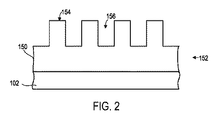
図1は、基板102上にレリーフパターンを形成するインプリントリソグラフィシステム100を図示する。基板102は、基板チャック104に結合され得る。いくつかの例では、基板チャック104は、真空チャック、ピンタイプチャック、溝タイプチャック、電磁チャック等を含み得る。いくつかの例では、基板102および基板チャック104は、空気ベアリング106上にさらに位置付けられ得る。空気ベアリング106は、x軸、y軸、および/またはz軸の周りの運動を提供する。いくつかの例では、基板102および基板チャック104は、段上に位置付けられる。空気ベアリング106、基板102、および基板チャック104は、基部108上にも位置付けられ得る。いくつかの例では、ロボットシステム110が、基板102を基板チャック104上に位置付ける。
FIG. 1 illustrates an
インプリントリソグラフィシステム100は、設計考慮事項に応じて、1つ以上のローラ114に結合されるインプリントリソグラフィ可撓テンプレート112をさらに含む。ローラ114は、可撓なテンプレート112の少なくとも一部の移動を提供する。そのような移動は、基板102と重なり合う可撓なテンプレート112の異なる部分を選択的に提供し得る。いくつかの例では、可撓なテンプレート112は、複数の特徴、例えば、間隔を置かれる陥凹部および突出部を含むパターン化表面を含む。しかしながら、いくつかの例では、特徴の他の構成も、可能である。パターン化表面は、基板102上に形成されるべきパターンの基礎を形成する任意の原パターンを画定し得る。いくつかの例では、可撓なテンプレート112は、テンプレートチャック、例えば、真空チャック、ピンタイプチャック、溝タイプチャック、電磁チャック等に結合され得る。
The
インプリントリソグラフィシステム100は、流体分注システム120をさらに備え得る。流体分注システム120は、基板102上に重合性材料を堆積させるために使用され得る。重合性材料は、液滴分注、スピンコーティング、浸漬コーティング、化学蒸着(CVD)、物理蒸着(PVD)、薄膜蒸着、厚膜蒸着等の技法を使用して基板102上に位置付けられ得る。いくつかの例では、重合性材料は、複数の液滴として基板102上に位置付けられる。
The
図1および2を参照すると、インプリントリソグラフィシステム100は、基板102に向かってエネルギーを向かわせるように結合されるエネルギー源122をさらに備えている。いくつかの例では、ローラ114および空気ベアリング106は、可撓なテンプレート112と基板102の所望される部分とを所望される位置に位置付けるように構成される。インプリントリソグラフィシステム100は、空気ベアリング106、ローラ114、流体分注システム120、および/またはエネルギー源122と通信するプロセッサによって調整され得、メモリ内に記憶されるコンピュータ読み取り可能なプログラムに基づいて動作し得る。
Referring to FIGS. 1 and 2, the
いくつかの例では、ローラ114、空気ベアリング106、または両方は、可撓なテンプレート112と基板102との間の距離を変動させ、それらの間に、重合性材料によって充填される所望される容積を画定する。例えば、可撓なテンプレート112は、重合性材料に接触する。所望される容積が重合性材料によって充填された後、エネルギー源122が、エネルギー、例えば、広帯域紫外線放射を生成し、重合性材料が凝固し、および/または架橋結合し、基板102の表面と可撓なテンプレート122のパターン化表面の一部との形状に適合し、基板102上にパターン化された層150を画定することも生じさせる。いくつかの例では、パターン化された層150は、残留層152と、突出部154および陥凹部156として示される複数の構造とを備え得る。
In some examples, the
図3は、インプリントリソグラフィシステム100を利用して形成され得る導波管300を図示する。手短に言えば、導波管300は、例えば、光(光ビーム)の源からそれを通過する光を捕捉し、光の全内部屈折を提供する。いくつかの例では、導波管300は、仮想コンテンツディスプレイの生成を促進する。導波管300は、パターン化層302と、第1の接着層304と、基板306と、反射防止層308と、第2の接着層310とを含む多層構造である。
FIG. 3 illustrates a
基板306が、第1の接着層304と反射防止層308との間に位置付けられる。基板306は、第1の屈折率に関連付けられ、いくつかの例では、ガラスまたはサファイアから作製される。いくつかの例では、第1の屈折率は、少なくとも1.7またはそれを上回る。第1の接着層304は、パターン化層302と基板306との間の接着を提供する。第1の接着層304は、アクリル樹脂のような材料から作製されることができる。
The
パターン化層302は、第1の接着層304が、パターン化層302と基板306との間にあるように位置付けられる。パターン化層302は、光硬化アクリルポリマー層を含み得る。パターン化層302は、第2の屈折率に関連付けられる。いくつかの例では、第1の屈折率は、第2の屈折率を上回る。いくつかの例では、第2の屈折率は、約1.5である。パターン化層302は、回折格子312と、残留層314とをさらに含む。いくつかの例では、残留層314は、100ナノメートルより小さい厚さを有し、さらに、いくつかの例では、50ナノメートルより小さい厚さを有する。回折格子312は、インプリントリソグラフィを含むそのような方法によって形成されることができ、約100ナノメートルの限界寸法を含むことができる。
The
その目的のために、基板306と回折格子312との間に位置付けられる残留層314を含む導波管300の結果として、導波管300は、回折ベースの導波管ディスプレイを画定することができる。特に、パターン化層302と基板306との組み合わせ、具体的には、第2の屈折率(例えば、約1.5)に関連付けられたパターン化層302と、第1の屈折率(例えば、1.7を上回る)に関連付けられた基板306との組み合わせが、回折ベースの導波管ディスプレイを提供する。さらに、回折ベースの導波管ディスプレイは、第2の屈折率(例えば、約1.5)に関連付けられたパターン化層302と、第1の屈折率(例えば、1.7を上回る)に関連付けられた基板306との組み合わせに基づいて回折ベースの導波管ディスプレイを形成することの結果として、基板306内に回折格子を形成することなく提供される。したがって、基板306をドライエッチングする(例えば、高屈折率ガラスまたはサファイアをドライエッチングする)必要性が、排除される。しかしながら、いくつかの例では、基板306が、残留層134を除去するために、および/または、基板306の表面上に残留層314の一部を維持しながら、パターンを基板306の中に移すために、部分的にエッチングされること(例えば、大気または低圧力条件下のプラズマプロセス)ができる。
For that purpose, the
いくつかの例では、100ナノメートル未満、または50ナノメートルより小さい厚さを有する残留層314の結果として、パターン化層302と基板306との間での屈折率整合が低減させられ、または最小化される。
In some examples, the index of refraction matching between the
導波管300は、第1および第2の屈折率に基づく視野に関連付けられる。すなわち、導波管300の視野は、パターン化層302に関連付けられた第2の屈折率と、基板306に関連付けられた第1の屈折率との組み合わせに基づく。いくつかの例では、導波管300の視野は、少なくとも50度である。すなわち、パターン化層302に関連付けられた第2の屈折率が約1.5であり、基板306に関連付けられた第1の屈折率が1.7を上回るとき、導波管300に関連付けられた視野は、少なくとも50度である。
The
反射防止層308は、基板306と第2の接着層310との間に位置付けられる。いくつかの例では、反射防止層308は、無機性である。反射防止層308および/またはパターン化層302は、基板306に環境保護/安定性を提供する。具体的には、基板306が高屈折率(例えば、1.7を上回る)を伴うガラス(またはサファイア)を含むとき、基板306は、環境にさらされると、基板306の表面に沈殿剤を形成し得る。結果として、薄霧汚染層が、形成し得(例えば、基板306の表面上に)、基板302の腐食が、生じ得、および/または、導波管300に関連付けられた散乱光が、増加し得る。その目的のために、反射防止層308および/またはパターン化層302は、基板306のイオン性表面(例えば、ガラス基板のイオン性表面)を隔離し、基板306の環境保護/安定性を提供する。
The
第2の接着層310は、反射防止層308と基板306との間の接着を提供する。いくつかの例では、第2の接着層310は、蒸着され、基板306(例えば、ガラス)に接合される。第2の接着層310は、アクリル樹脂のような材質から作製されることができる。
The second
図4は、導波管402を連続的に通過する光を捕捉するために積み重ねられた複数の導波管402a、402b、402c(集合的に導波管402と称される)を含む多重導波管光学構造400を図示する。導波管402の各々は、図3の導波管302に類似し得る。いくつかの例では、導波管402の各々は、平面の異なる色および異なる深度に関連付けられた。すなわち、光が導波管402の各々を通過するにつれて、導波管402の各々は、異なるように光と相互作用し、導波管402の各退出光は、仮想コンテンツディスプレイに関連付けられた平面の異なる色および異なる深度に基づく。いくつかの例では、多重導波管光学構造400は、6個または9個の導波管402を含む4個以上の導波管402を含む。いくつかの例では、多重導波管光学構造400の導波管402の各々は、空気によって分離される。
FIG. 4 shows multiple conductions including a plurality of
多重導波管光学構造400は、導波管支持部404a、404b(集合的に導波管支持部404と称される)を含む。導波管支持部404は、複数の導波管402を多重導波管光学構造400の内に接続かつ位置付ける。その目的のために、導波管402の各々の第1の接着層304および第2の接着層310は、それぞれの導波管402と導波管支持部404との間の接着を提供する。導波管支持部404は、アクリル樹脂またはエポキシ樹脂のような材料から作製されることができる。いくつかの例では、パターン化層302は、それぞれの導波管402と導波管支持部404との間の追加の接合を提供する。
The multiple waveguide
図5は、追加のパターン化層を含む導波管500を図示する。具体的には、導波管500は、第1のパターン化層502と、第1の接着層504と、基板506と、反射防止層508と、第2の接着層510と、第2のパターン化層512とを含む。第1のパターン化層502、第1の接着層504、基板506、反射防止層508、および第2の接着層510は、図3の導波管300のパターン化層302、第1の接着層304、基板306、反射防止層308、および第2の接着層310とほぼ類似する。
FIG. 5 illustrates a
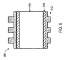
さらに、第2のパターン化層512は、第2の接着層510が反射防止層508と第2のパターン化層512との間にあるように位置付けられる。第2の接着層510は、第2のパターン化層512と基板506との間の接着を提供する。いくつかの例では、図6に示されるように、導波管500’は、反射防止層508を欠き、したがって、第2の接着層510が、基板506と第2のパターン化層512との間に位置付けられるように第2のパターン化層512を含む。
Further, the second
第2のパターン化層512は、図3のパターン化層302にほぼ類似する。具体的には、第2のパターン化層512は、第3の屈折率に関連付けられる。いくつかの例では、基板506に関連付けられた第1の屈折率は、第2のパターン化層512に関連付けられた第3の屈折率を上回る。いくつかの例では、第3の屈折率は、約1.5である。第2のパターン化層512は、回折格子514と、50ナノメートルより小さい厚さを有する残留層516とをさらに含む。回折格子514は、インプリントリソグラフィを含むそのような方法によって形成されることができ、約100ナノメートルの限界寸法を含むことができる。
The
その目的のために、基板506と回折格子514との間に位置付けられる残留層516を含む導波管500の結果として、導波管500は、回折ベースの導波管ディスプレイを画定することができる。特に、第2のパターン化層512と基板506との組み合わせ、具体的には、第3の屈折率(例えば、約1.5)に関連付けられた2のパターン化層512と、第1の屈折率(例えば、1.7を上回る)に関連付けられた基板506との組み合わせが、回折ベースの導波管ディスプレイを提供する。そのうえ、回折ベースの導波管ディスプレイは、第3の屈折率(例えば、約1.5)に関連付けられた第2のパターン化層512と、第1の屈折率(例えば、1.7を上回る)に関連付けられた基板506との組み合わせに基づく回折ベースの導波管ディスプレイの形成の結果として、基板506内に回折格子を形成することなく、提供される。したがって、基板506をドライエッチングする(例えば、高屈折率ガラスまたはサファイアをドライエッチングする)必要性が、排除される。
To that end, the
いくつかの例では、第1のパターン化層502、第2のパターン化層512、および基板506の組み合わせ、具体的には、第1の屈折率(例えば、約1.5)に関連付けられた第1のパターン化層502と、第3の屈折率(例えば、約1.5)に関連付けられた第2のパターン化層512と、第1の屈折率(例えば、1.7を上回る)に関連付けられた基板506との組み合わせが、回折ベースの導波管ディスプレイを提供する。
In some examples, it was associated with a combination of a first
導波管500は、第1および第3の屈折率に基づく視野に関連付けられる。すなわち、導波管500の視野は、第2のパターン化層512に関連付けられた第3の屈折率と、基板506に関連付けられた第1の屈折率との組み合わせに基づく。いくつかの例では、導波管500の視野は、少なくとも50度である。すなわち、第2のパターン化層512に関連付けられた第3の屈折率が、約1.5であり、かつ基板506に関連付けられた第1の屈折率が、1.7を上回るとき、導波管500に関連付けられた視野は、少なくとも50度である。いくつかの例では、導波管500の視野は、第1のパターン化層502に関連付けられた第2の屈折率と、第2のパターン化層512に関連付けられた第3の屈折率と、基板506に関連付けられた第1の屈折率との組み合わせに基づく。
The
いくつかの例では、図4の多重導波管光学構造400の導波管402の各々は、図5の導波管500および/または図6の導波管500’に類似し得る。いくつかの例では、多重導波管光学構造400の導波管402は、図3の導波管300と、図5の導波管500と、図6の導波管500’との任意の組み合わせに類似し得る。
In some examples, each of the waveguides 402 in the multiple waveguide
図1のインプリントリソグラフィシステム100は、導波管302、402、500、500’、および/または多重導波管光学構造400のうちのいずれかを形成するために使用されることができる。
The
Claims (18)
各導波管を連続的に通過する光を捕捉するために積み重ねられた複数の導波管を備え、各導波管は、平面の異なる色および異なる深度に関連付けられており、各導波管は、
第1の接着層と、
第1の屈折率を有する基板と、
パターン化層と
を備え、
前記パターン化層は、前記第1の接着層が前記パターン化層と前記基板との間にあるように位置付けられ、前記第1の接着層は、前記パターン化層と前記基板との間の接着を提供し、前記パターン化層は、前記第1の屈折率より小さい第2の屈折率を有し、前記パターン化層は、回折格子を画定し、前記導波管に関連付けられた視野は、前記第1および前記第2の屈折率に基づき、
前記各導波管は、第2の接着層をさらに備え、前記第2の接着層は、前記基板が前記第1の接着層と前記第2の接着層との間にあるように位置付けられており、各導波管は、前記基板と前記第2の接着層との間に位置付けられた反射防止層をさらに備えている、多重導波管光学構造。 It is a multiple waveguide optical structure, and the multiple waveguide optical structure is
Each waveguide is associated with a different color and different depth of plane, with multiple waveguides stacked to capture light passing continuously through each waveguide. teeth,
With the first adhesive layer,
A substrate having a first refractive index and
With a patterning layer,
The patterned layer is positioned such that the first adhesive layer is between the patterned layer and the substrate, and the first adhesive layer is an adhesion between the patterned layer and the substrate. The patterned layer has a second index of refraction that is smaller than the first index of refraction, the patterned layer defines a diffraction grating, and the field of view associated with the waveguide is: wherein based-out in the first and the second refractive index,
Each waveguide further comprises a second adhesive layer, wherein the second adhesive layer is positioned such that the substrate is between the first adhesive layer and the second adhesive layer. Each waveguide further comprises an antireflection layer located between the substrate and the second adhesive layer , a multiple waveguide optical structure.
各導波管を連続的に通過する光を捕捉するために積み重ねられた複数の導波管を備え、各導波管は、平面の異なる色および異なる深度に関連付けられており、各導波管は、
第1の接着層と、
反射防止層と、
前記第1の接着層と前記反射防止層との間に位置付けられた基板であって、前記基板は、第1の屈折率を有する、基板と、
第1のパターン化層であって、前記第1のパターン化層は、前記第1の接着層が前記第1のパターン化層と前記基板との間にあるように位置付けられ、前記第1の接着層は、前記第1のパターン化層と前記基板との間の接着を提供し、前記第1のパターン化層は、前記第1の屈折率より小さい第2の屈折率を有し、前記第1のパターン化層は、回折格子を画定し、前記導波管に関連付けられた視野は、前記第1および前記第2の屈折率に基づく、第1のパターン化層と、
第2の接着層と、
第2のパターン化層と
を備え、
前記第2のパターン化層は、前記第2の接着層が前記反射防止層と前記第2のパターン化層との間に位置付けられるように位置付けられ、前記第2の接着層は、前記第2のパターン化層と前記反射防止層との間の接着を提供し、
前記反射防止層は、前記基板と前記第2の接着層との間に位置付けられている、多重導波管光学構造。 It is a multiple waveguide optical structure, and the multiple waveguide optical structure is
Each waveguide is associated with a different color and different depth of plane, with multiple waveguides stacked to capture light passing continuously through each waveguide. teeth,
With the first adhesive layer,
Anti-reflective layer and
A substrate positioned between the first adhesive layer and the antireflection layer, wherein the substrate has a first refractive index and the substrate.
The first patterning layer, wherein the first patterning layer is positioned so that the first adhesive layer is between the first patterning layer and the substrate, and the first patterning layer is described. The adhesive layer provides adhesion between the first patterned layer and the substrate, the first patterned layer having a second refractive index smaller than the first refractive index, said. The first patterned layer defines a diffraction grating, and the field of view associated with the waveguide is the first patterned layer, which is based on the first and second refractive indexes.
With the second adhesive layer,
With a second patterning layer
The second patterned layer is positioned so that the second adhesive layer is positioned between the antireflection layer and the second patterned layer, and the second adhesive layer is the second adhesive layer. Provides adhesion between the patterned layer and the antireflection layer .
The antireflection layer is a multiple waveguide optical structure positioned between the substrate and the second adhesive layer.
各導波管を連続的に通過する光を捕捉するために積み重ねられた複数の導波管を備え、各導波管は、平面の異なる色および異なる深度に関連付けられており、各導波管は、
第1の接着層と、
反射防止層と、
前記第1の接着層と前記反射防止層との間に位置付けられた基板であって、前記基板は、第1の屈折率を有する、基板と、
パターン化層であって、前記パターン化層は、前記第1の接着層が前記パターン化層と前記基板との間にあるように位置付けられ、前記第1の接着層は、前記パターン化層と前記基板との間の接着を提供し、前記パターン化層は、前記第1の屈折率より小さい第2の屈折率を有し、前記パターン化層は、回折格子を画定し、前記導波管に関連付けられた視野は、前記第1および前記第2の屈折率に基づく、パターン化層と、
第2の接着層であって、前記第2の接着層は、前記反射防止層が前記第2の接着層と前記基板との間に位置付けられるように位置付けられている、第2の接着層と、
前記複数の導波管の各導波管を接続し、位置付ける導波管支持部と
を備え、
各導波管の前記第1および第2の接着層のうちの少なくとも1つが、前記導波管支持部に接着している、多重導波管光学構造。 It is a multiple waveguide optical structure, and the multiple waveguide optical structure is
Each waveguide is associated with a different color and different depth of plane, with multiple waveguides stacked to capture light passing continuously through each waveguide. teeth,
With the first adhesive layer,
Anti-reflective layer and
A substrate positioned between the first adhesive layer and the antireflection layer, wherein the substrate has a first refractive index and the substrate.
The patterned layer is positioned such that the first adhesive layer is located between the patterned layer and the substrate, and the first adhesive layer is the patterned layer. Providing adhesion to the substrate, the patterned layer has a second index of refraction that is smaller than the first index of refraction, the patterned layer defining a diffraction grating and the waveguide. The visual field associated with the patterning layer, which is based on the first and second refractive indexes,
A second adhesive layer, wherein the second adhesive layer is a second adhesive layer in which the antireflection layer is positioned so as to be positioned between the second adhesive layer and the substrate. ,
Each waveguide of the plurality of waveguides is connected and provided with a waveguide support for positioning.
A multiple waveguide optical structure in which at least one of the first and second adhesive layers of each waveguide is bonded to the waveguide support.
Applications Claiming Priority (3)
| Application Number | Priority Date | Filing Date | Title |
|---|---|---|---|
| US201662428193P | 2016-11-30 | 2016-11-30 | |
| US62/428,193 | 2016-11-30 | ||
| PCT/US2017/051796 WO2018102005A1 (en) | 2016-11-30 | 2017-09-15 | Multi-waveguide light field display |
Publications (3)
| Publication Number | Publication Date |
|---|---|
| JP2020507793A JP2020507793A (en) | 2020-03-12 |
| JP2020507793A5 JP2020507793A5 (en) | 2020-10-22 |
| JP6967593B2 true JP6967593B2 (en) | 2021-11-17 |
Family
ID=62189986
Family Applications (1)
| Application Number | Title | Priority Date | Filing Date |
|---|---|---|---|
| JP2019528690A Active JP6967593B2 (en) | 2016-11-30 | 2017-09-15 | Multiple waveguide brightfield display |
Country Status (9)
| Country | Link |
|---|---|
| US (3) | US10444422B2 (en) |
| EP (1) | EP3548941A4 (en) |
| JP (1) | JP6967593B2 (en) |
| KR (1) | KR102247455B1 (en) |
| CN (2) | CN110023801B (en) |
| AU (1) | AU2017367795B2 (en) |
| CA (1) | CA3044808A1 (en) |
| IL (3) | IL266824B2 (en) |
| WO (1) | WO2018102005A1 (en) |
Families Citing this family (10)
| Publication number | Priority date | Publication date | Assignee | Title |
|---|---|---|---|---|
| CA3044808A1 (en) * | 2016-11-30 | 2018-06-07 | Molecular Imprints, Inc. | Multi-waveguide light field display |
| US11536882B2 (en) * | 2017-07-18 | 2022-12-27 | Baden-Württemberg Stiftung Ggmbh | Method of fabricating an imaging system and corresponding imaging system |
| US10705268B2 (en) * | 2018-06-29 | 2020-07-07 | Applied Materials, Inc. | Gap fill of imprinted structure with spin coated high refractive index material for optical components |
| US11635622B1 (en) * | 2018-12-07 | 2023-04-25 | Meta Platforms Technologies, Llc | Nanovided spacer materials and corresponding systems and methods |
| KR20230019080A (en) * | 2020-04-07 | 2023-02-07 | 스냅 인코포레이티드 | optical device |
| EP4200657A1 (en) * | 2020-09-08 | 2023-06-28 | Sony Group Corporation | Waveguide with diffraction grating, head mounted device comprising diffraction grating and template for imprinting optical gratings |
| CN112331071A (en) * | 2020-10-23 | 2021-02-05 | 云谷(固安)科技有限公司 | Light field modulation assembly, display assembly and display device |
| CN117063104A (en) * | 2020-11-17 | 2023-11-14 | 应用材料公司 | Optical device with structure and graded refractive index and method of manufacturing the same |
| US11926113B2 (en) * | 2022-08-03 | 2024-03-12 | Himax Technologies Limited | Optical element and method for manufacturing optical element |
| CN115032734B (en) * | 2022-08-11 | 2023-01-24 | 歌尔光学科技有限公司 | Optical waveguide structure, manufacturing method and electronic equipment |
Family Cites Families (23)
| Publication number | Priority date | Publication date | Assignee | Title |
|---|---|---|---|---|
| US6785447B2 (en) * | 1998-10-09 | 2004-08-31 | Fujitsu Limited | Single and multilayer waveguides and fabrication process |
| EP1849620B1 (en) * | 2000-01-21 | 2016-03-23 | Viavi Solutions Inc. | Optically variable security devices |
| US6307995B1 (en) * | 2000-04-05 | 2001-10-23 | James T. Veligdan | Planar optical waveguides for optical panel having gradient refractive index core |
| JP2003302514A (en) * | 2002-04-09 | 2003-10-24 | Ricoh Co Ltd | Diffraction optical element, method for manufacturing the same, optical pickup device and optical disk drive device |
| JP3885671B2 (en) * | 2002-06-20 | 2007-02-21 | 住友電気工業株式会社 | Planar waveguide type diffraction grating element manufacturing method |
| US7187831B2 (en) * | 2004-04-26 | 2007-03-06 | Brookhaven Science Associates | Optical panel system including stackable waveguides |
| GB0422266D0 (en) * | 2004-10-07 | 2004-11-10 | Suisse Electronique Microtech | Security device |
| JP2007058945A (en) * | 2005-08-22 | 2007-03-08 | Fujifilm Corp | Optical memory |
| US7784954B1 (en) * | 2006-07-25 | 2010-08-31 | Fusion Optix, Inc. | Polarization sensitive light homogenizer |
| JP2008058907A (en) * | 2006-09-04 | 2008-03-13 | Canon Inc | Diffractive optical element and optical system having the same |
| US7548671B2 (en) * | 2007-07-16 | 2009-06-16 | Hewlett-Packard Development Company, L.P. | Optical device including waveguide grating structure |
| US20090148619A1 (en) * | 2007-12-05 | 2009-06-11 | Molecular Imprints, Inc. | Controlling Thickness of Residual Layer |
| JP5462443B2 (en) * | 2008-03-27 | 2014-04-02 | 株式会社東芝 | Reflective screen, display device and moving body |
| US11320571B2 (en) * | 2012-11-16 | 2022-05-03 | Rockwell Collins, Inc. | Transparent waveguide display providing upper and lower fields of view with uniform light extraction |
| JP5834458B2 (en) * | 2011-04-13 | 2015-12-24 | 株式会社ニコン | Optical element manufacturing method and optical element |
| US9933684B2 (en) * | 2012-11-16 | 2018-04-03 | Rockwell Collins, Inc. | Transparent waveguide display providing upper and lower fields of view having a specific light output aperture configuration |
| US9477033B2 (en) * | 2013-04-23 | 2016-10-25 | Lumenco, Llc | Multi-layered waveguide for capturing solar energy |
| US10677969B2 (en) * | 2013-11-27 | 2020-06-09 | Magic Leap, Inc. | Manufacturing for virtual and augmented reality systems and components |
| US9915826B2 (en) | 2013-11-27 | 2018-03-13 | Magic Leap, Inc. | Virtual and augmented reality systems and methods having improved diffractive grating structures |
| JP6234208B2 (en) * | 2013-12-18 | 2017-11-22 | マイクロソフト テクノロジー ライセンシング,エルエルシー | NED polarization system for wavelength passage |
| JP2015184561A (en) * | 2014-03-25 | 2015-10-22 | ソニー株式会社 | Light guide device, image display device, and display device |
| KR102688893B1 (en) * | 2014-09-29 | 2024-07-29 | 매직 립, 인코포레이티드 | Architectures and methods for outputting different wavelength light out of waveguides |
| CA3044808A1 (en) | 2016-11-30 | 2018-06-07 | Molecular Imprints, Inc. | Multi-waveguide light field display |
-
2017
- 2017-09-15 CA CA3044808A patent/CA3044808A1/en active Pending
- 2017-09-15 AU AU2017367795A patent/AU2017367795B2/en active Active
- 2017-09-15 CN CN201780073732.5A patent/CN110023801B/en active Active
- 2017-09-15 IL IL266824A patent/IL266824B2/en unknown
- 2017-09-15 IL IL304058A patent/IL304058A/en unknown
- 2017-09-15 WO PCT/US2017/051796 patent/WO2018102005A1/en unknown
- 2017-09-15 KR KR1020197018780A patent/KR102247455B1/en active IP Right Grant
- 2017-09-15 EP EP17876076.5A patent/EP3548941A4/en active Pending
- 2017-09-15 JP JP2019528690A patent/JP6967593B2/en active Active
- 2017-09-15 US US15/705,838 patent/US10444422B2/en active Active
- 2017-09-15 IL IL313192A patent/IL313192A/en unknown
- 2017-09-15 CN CN202111171261.6A patent/CN113866876B/en active Active
-
2019
- 2019-10-11 US US16/599,782 patent/US11181681B2/en active Active
-
2021
- 2021-10-19 US US17/451,366 patent/US11630257B2/en active Active
Also Published As
| Publication number | Publication date |
|---|---|
| EP3548941A4 (en) | 2019-12-18 |
| IL304058A (en) | 2023-08-01 |
| IL266824B2 (en) | 2023-12-01 |
| WO2018102005A1 (en) | 2018-06-07 |
| JP2020507793A (en) | 2020-03-12 |
| US20180149796A1 (en) | 2018-05-31 |
| US20220035091A1 (en) | 2022-02-03 |
| CN110023801B (en) | 2021-10-26 |
| IL266824A (en) | 2019-07-31 |
| IL313192A (en) | 2024-07-01 |
| EP3548941A1 (en) | 2019-10-09 |
| IL266824B1 (en) | 2023-08-01 |
| AU2017367795B2 (en) | 2022-02-03 |
| KR102247455B1 (en) | 2021-04-30 |
| CN113866876A (en) | 2021-12-31 |
| NZ753485A (en) | 2023-08-25 |
| US10444422B2 (en) | 2019-10-15 |
| US20200124782A1 (en) | 2020-04-23 |
| US11181681B2 (en) | 2021-11-23 |
| KR20190082978A (en) | 2019-07-10 |
| AU2017367795A1 (en) | 2019-05-30 |
| US11630257B2 (en) | 2023-04-18 |
| CN113866876B (en) | 2024-03-19 |
| CA3044808A1 (en) | 2018-06-07 |
| CN110023801A (en) | 2019-07-16 |
Similar Documents
| Publication | Publication Date | Title |
|---|---|---|
| JP6967593B2 (en) | Multiple waveguide brightfield display | |
| JP7008157B2 (en) | Optical layer configuration in the imprint lithography process | |
| KR20160101104A (en) | Improvements in and relating to waveguides | |
| KR20160101110A (en) | Improvements in and relating to waveguides | |
| KR102129858B1 (en) | Diffractive optical element, manufacturing method thereof and optical device having the same | |
| JP2013210680A (en) | Diffraction optical element, method of manufacturing the same, and laser machining method | |
| JP2020507793A5 (en) | ||
| JP2022536694A (en) | Optical eyepiece using single-sided patterning of grating couplers | |
| US20100208346A1 (en) | Multilayer Dielectric Transmission Gratings Having Maximal Transmitted Diffraction Efficiency | |
| JP4178583B2 (en) | Anti-reflection coating | |
| NZ753485B2 (en) | Multi-waveguide light field display | |
| US11237479B2 (en) | Configuring optical layers in imprint lithography processes | |
| JP2020501183A (en) | Creating a virtual content display |
Legal Events
| Date | Code | Title | Description |
|---|---|---|---|
| A521 | Request for written amendment filed |
Free format text: JAPANESE INTERMEDIATE CODE: A523 Effective date: 20200914 |
|
| A621 | Written request for application examination |
Free format text: JAPANESE INTERMEDIATE CODE: A621 Effective date: 20200914 |
|
| A871 | Explanation of circumstances concerning accelerated examination |
Free format text: JAPANESE INTERMEDIATE CODE: A871 Effective date: 20200914 |
|
| A977 | Report on retrieval |
Free format text: JAPANESE INTERMEDIATE CODE: A971007 Effective date: 20201218 |
|
| A975 | Report on accelerated examination |
Free format text: JAPANESE INTERMEDIATE CODE: A971005 Effective date: 20201214 |
|
| A131 | Notification of reasons for refusal |
Free format text: JAPANESE INTERMEDIATE CODE: A131 Effective date: 20210202 |
|
| A601 | Written request for extension of time |
Free format text: JAPANESE INTERMEDIATE CODE: A601 Effective date: 20210420 |
|
| A521 | Request for written amendment filed |
Free format text: JAPANESE INTERMEDIATE CODE: A523 Effective date: 20210702 |
|
| TRDD | Decision of grant or rejection written | ||
| A01 | Written decision to grant a patent or to grant a registration (utility model) |
Free format text: JAPANESE INTERMEDIATE CODE: A01 Effective date: 20210927 |
|
| A61 | First payment of annual fees (during grant procedure) |
Free format text: JAPANESE INTERMEDIATE CODE: A61 Effective date: 20211025 |
|
| R150 | Certificate of patent or registration of utility model |
Ref document number: 6967593 Country of ref document: JP Free format text: JAPANESE INTERMEDIATE CODE: R150 |
|
| R250 | Receipt of annual fees |
Free format text: JAPANESE INTERMEDIATE CODE: R250 |