JP6965732B2 - Bandpass filter - Google Patents

Bandpass filter Download PDF

Info

Publication number
JP6965732B2
JP6965732B2 JP2017249867A JP2017249867A JP6965732B2 JP 6965732 B2 JP6965732 B2 JP 6965732B2 JP 2017249867 A JP2017249867 A JP 2017249867A JP 2017249867 A JP2017249867 A JP 2017249867A JP 6965732 B2 JP6965732 B2 JP 6965732B2
Authority
JP
Japan
Prior art keywords
resonator
conductor
resonators
holes
bandpass filter
Prior art date
Legal status (The legal status is an assumption and is not a legal conclusion. Google has not performed a legal analysis and makes no representation as to the accuracy of the status listed.)
Active
Application number
JP2017249867A
Other languages
Japanese (ja)
Other versions
JP2019117970A (en
Inventor
裕太 芦田
憲幸 平林
重光 戸蒔
Current Assignee (The listed assignees may be inaccurate. Google has not performed a legal analysis and makes no representation or warranty as to the accuracy of the list.)
TDK Corp
Original Assignee
TDK Corp
Priority date (The priority date is an assumption and is not a legal conclusion. Google has not performed a legal analysis and makes no representation as to the accuracy of the date listed.)
Filing date
Publication date
Application filed by TDK Corp filed Critical TDK Corp
Priority to JP2017249867A priority Critical patent/JP6965732B2/en
Priority to US16/179,059 priority patent/US10784551B2/en
Priority to CN201811599319.5A priority patent/CN110011006B/en
Publication of JP2019117970A publication Critical patent/JP2019117970A/en
Application granted granted Critical
Publication of JP6965732B2 publication Critical patent/JP6965732B2/en
Active legal-status Critical Current
Anticipated expiration legal-status Critical

Links

Images

Classifications

    • HELECTRICITY
    • H01ELECTRIC ELEMENTS
    • H01PWAVEGUIDES; RESONATORS, LINES, OR OTHER DEVICES OF THE WAVEGUIDE TYPE
    • H01P1/00Auxiliary devices
    • H01P1/20Frequency-selective devices, e.g. filters
    • H01P1/201Filters for transverse electromagnetic waves
    • H01P1/203Strip line filters
    • H01P1/20327Electromagnetic interstage coupling
    • H01P1/20336Comb or interdigital filters
    • H01P1/20345Multilayer filters
    • HELECTRICITY
    • H01ELECTRIC ELEMENTS
    • H01PWAVEGUIDES; RESONATORS, LINES, OR OTHER DEVICES OF THE WAVEGUIDE TYPE
    • H01P1/00Auxiliary devices
    • H01P1/20Frequency-selective devices, e.g. filters
    • HELECTRICITY
    • H01ELECTRIC ELEMENTS
    • H01PWAVEGUIDES; RESONATORS, LINES, OR OTHER DEVICES OF THE WAVEGUIDE TYPE
    • H01P1/00Auxiliary devices
    • H01P1/20Frequency-selective devices, e.g. filters
    • H01P1/201Filters for transverse electromagnetic waves
    • H01P1/203Strip line filters
    • H01P1/20309Strip line filters with dielectric resonator
    • HELECTRICITY
    • H01ELECTRIC ELEMENTS
    • H01PWAVEGUIDES; RESONATORS, LINES, OR OTHER DEVICES OF THE WAVEGUIDE TYPE
    • H01P1/00Auxiliary devices
    • H01P1/20Frequency-selective devices, e.g. filters
    • H01P1/201Filters for transverse electromagnetic waves
    • H01P1/203Strip line filters
    • H01P1/20327Electromagnetic interstage coupling
    • H01P1/20354Non-comb or non-interdigital filters
    • H01P1/20381Special shape resonators
    • HELECTRICITY
    • H01ELECTRIC ELEMENTS
    • H01PWAVEGUIDES; RESONATORS, LINES, OR OTHER DEVICES OF THE WAVEGUIDE TYPE
    • H01P1/00Auxiliary devices
    • H01P1/20Frequency-selective devices, e.g. filters
    • H01P1/201Filters for transverse electromagnetic waves
    • H01P1/203Strip line filters
    • H01P1/2039Galvanic coupling between Input/Output
    • HELECTRICITY
    • H03ELECTRONIC CIRCUITRY
    • H03HIMPEDANCE NETWORKS, e.g. RESONANT CIRCUITS; RESONATORS
    • H03H7/00Multiple-port networks comprising only passive electrical elements as network components
    • H03H7/01Frequency selective two-port networks
    • H03H7/0115Frequency selective two-port networks comprising only inductors and capacitors
    • HELECTRICITY
    • H03ELECTRONIC CIRCUITRY
    • H03HIMPEDANCE NETWORKS, e.g. RESONANT CIRCUITS; RESONATORS
    • H03H7/00Multiple-port networks comprising only passive electrical elements as network components
    • H03H7/01Frequency selective two-port networks
    • H03H7/0153Electrical filters; Controlling thereof
    • H03H7/0161Bandpass filters

Description

本発明は、複数の共振器とシールドを含むバンドパスフィルタに関する。 The present invention relates to a bandpass filter that includes a plurality of resonators and shields.

現在、第5世代移動通信システム(以下、5Gと言う。)の規格化が進められている。5Gでは、周波数帯域を拡大するために、10GHz以上の周波数帯域、特に、10〜30GHzの準ミリ波帯や30〜300GHzのミリ波帯の利用が検討されている。 Currently, standardization of the 5th generation mobile communication system (hereinafter referred to as 5G) is in progress. In 5G, in order to expand the frequency band, the use of a frequency band of 10 GHz or more, particularly a quasi-millimeter wave band of 10 to 30 GHz and a millimeter wave band of 30 to 300 GHz is being studied.

通信装置に用いられる電子部品の一つには、複数の共振器を備えたバンドパスフィルタがある。複数の共振器の各々は、例えば、一方向に長い導体部を有している。また、バンドパスフィルタには、周囲へ電磁波が放射されることを防止するために、複数の共振器をシールドで囲った構造のものがある。 One of the electronic components used in a communication device is a bandpass filter having a plurality of resonators. Each of the plurality of resonators has, for example, a conductor portion that is long in one direction. Further, some bandpass filters have a structure in which a plurality of resonators are surrounded by a shield in order to prevent electromagnetic waves from being radiated to the surroundings.

特許文献1には、準ミリ波帯やミリ波帯での使用が可能なチップ型多段フィルタ装置が記載されている。このチップ型多段フィルタ装置は、複数の誘電体層を積層してなる多層基板と、第1および第2の表面グラウンド電極と、第1および第2の内部グラウンド電極と、第1および第2のλ/2共振器電極とを備えている。多層基板は、対向する第1および第2の主面と、第1および第2の主面を連結する第1ないし第4の側面を有している。第1の側面と第2の側面は対向している。第1の表面グラウンド電極は、第1の側面に設けられている。第2の表面グラウンド電極は、第2の側面に設けられている。第1の内部グラウンド電極は、多層基板内において、第1の主面に相対的に近い誘電体層に設けられている。第2の内部グラウンド電極は、多層基板内において、第2の主面に相対的に近い誘電体層に設けられている。第1および第2のλ/2共振器電極は、第1および第2の表面グラウンド電極と第1および第2の内部グラウンド電極によって囲まれた領域に配置されている。 Patent Document 1 describes a chip-type multi-stage filter device that can be used in a quasi-millimeter wave band or a millimeter wave band. This chip-type multi-stage filter device includes a multilayer substrate formed by laminating a plurality of dielectric layers, first and second surface ground electrodes, first and second internal ground electrodes, and first and second surfaces. It is equipped with a λ / 2 resonator electrode. The multilayer substrate has first and second main surfaces facing each other and first to fourth side surfaces connecting the first and second main surfaces. The first side surface and the second side surface face each other. The first surface ground electrode is provided on the first side surface. The second surface ground electrode is provided on the second side surface. The first internal ground electrode is provided in a dielectric layer relatively close to the first main surface in the multilayer substrate. The second internal ground electrode is provided in the dielectric layer relatively close to the second main surface in the multilayer substrate. The first and second λ / 2 resonator electrodes are located in a region surrounded by the first and second surface ground electrodes and the first and second internal ground electrodes.

特許文献1に記載されたチップ型多段フィルタ装置は、更に、ビアホール導体と、容量ユニットを備えている。ビアホール導体は、第1および第2の内部グラウンド電極を電気的に接続するように複数の誘電体層のうちの少なくとも一部の誘電体層を貫通するように設けられている。第1および第2のλ/2共振器電極は、ビアホール導体を介して対向配置されている。容量ユニットは、第1および第2のλ/2共振器電極間に結合容量を付加するために多層基板内に設けられている。 The chip-type multi-stage filter device described in Patent Document 1 further includes a via hole conductor and a capacitance unit. The via hole conductor is provided so as to penetrate at least a part of the dielectric layers so as to electrically connect the first and second internal ground electrodes. The first and second λ / 2 resonator electrodes are arranged to face each other via a via hole conductor. The capacitance unit is provided in the multilayer substrate to add a coupling capacitance between the first and second λ / 2 resonator electrodes.

特開2006−311100号公報Japanese Unexamined Patent Publication No. 2006-311100

複数の共振器をシールドで囲った構造のバンドパスフィルタでは、シールドとその内側の誘電体によって導波管に似た構造が形成されることによって、1つ以上の電磁波の伝搬モードが生じる。以下、この電磁波の伝搬モードを導波管モードと言う。バンドパスフィルタでは、この導波管モードによって、通過帯域よりも高い周波数領域に存在する共振周波数を有する不要な共振が生じて、通過帯域よりも高い周波数領域における減衰特性が悪化するという問題が生じていた。特に、通過帯域が準ミリ波帯やミリ波帯に存在するように設計されたバンドパスフィルタでは、共振周波数が最も低い導波管モード(以下、最低次導波管モードと言う。)の共振周波数であっても、通過帯域に比較的近くなるため、上記の問題が顕著になっていた。 In a bandpass filter having a structure in which a plurality of resonators are surrounded by a shield, one or more electromagnetic wave propagation modes are generated by forming a structure similar to a waveguide by the shield and the dielectric material inside the shield. Hereinafter, this electromagnetic wave propagation mode is referred to as a waveguide mode. In the bandpass filter, this waveguide mode causes a problem that unnecessary resonance having a resonance frequency existing in a frequency region higher than the pass band is generated, and the attenuation characteristic in the frequency region higher than the pass band is deteriorated. Was there. In particular, in a bandpass filter designed so that the pass band exists in the quasi-millimeter wave band or the millimeter wave band, the resonance of the waveguide mode having the lowest resonance frequency (hereinafter referred to as the lowest-order waveguide mode). Even if the frequency is relatively close to the pass band, the above problem has become remarkable.

最低次導波管モードの共振周波数は、シールドで囲まれた空間の形状によって変化する。一般的に、この空間が大きいほど、最低次導波管モードの共振周波数は低くなる。 The resonant frequency of the lowest-order waveguide mode varies depending on the shape of the space enclosed by the shield. In general, the larger this space, the lower the resonance frequency in the lowest-order waveguide mode.

特許文献1には、ビアホール導体によって、外形形状に起因する共振を抑制することができる旨が記載されている。外形形状に起因する共振は、上述の導波管モードに起因する共振に対応する。 Patent Document 1 describes that a via hole conductor can suppress resonance caused by an external shape. The resonance caused by the outer shape corresponds to the resonance caused by the above-mentioned waveguide mode.

しかし、特許文献1に記載されたフィルタ装置では、以下のような問題点がある。このフィルタ装置では、回路構成上隣接して容量結合する2つのλ/2共振器電極の間にビアホール導体が配置されている。一般的に、回路構成上隣接する2つの共振器が結合するように構成されたバンドパスフィルタでは、回路構成上隣接する2つの共振器の間には強い結合が必要である。特許文献1に記載されたフィルタ装置では、回路構成上隣接する2つのλ/2共振器電極の間に強い容量結合を生じさせることと、その2つのλ/2共振器電極の間にビアホール導体を配置することとを、バンドパスフィルタの特性を劣化させることなく両立させることが難しいという問題点がある。 However, the filter device described in Patent Document 1 has the following problems. In this filter device, a via hole conductor is arranged between two λ / 2 resonator electrodes that are capacitively coupled adjacent to each other in the circuit configuration. Generally, in a bandpass filter configured so that two resonators adjacent to each other in the circuit configuration are coupled, a strong coupling is required between the two resonators adjacent to each other in the circuit configuration. In the filter device described in Patent Document 1, a strong capacitive coupling is generated between two λ / 2 resonator electrodes adjacent to each other in the circuit configuration, and a via hole conductor is formed between the two λ / 2 resonator electrodes. There is a problem that it is difficult to make the arrangement of the bandpass filter compatible with each other without deteriorating the characteristics of the bandpass filter.

本発明はかかる問題点に鑑みてなされたもので、その目的は、複数の共振器とシールドを含み、良好な特性を有するバンドパスフィルタを提供することにある。 The present invention has been made in view of such problems, and an object of the present invention is to provide a bandpass filter including a plurality of resonators and a shield and having good characteristics.

本発明のバンドパスフィルタは、誘電体よりなる本体と、本体に一体化された第1の入出力ポートおよび第2の入出力ポートと、3つ以上の共振器と、シールドと、仕切り部とを備えている。3つ以上の共振器は、本体内に設けられていると共に、回路構成上第1の入出力ポートと第2の入出力ポートの間に設けられ、回路構成上隣接する2つの共振器が電磁結合するように構成されている。シールドは、導体よりなり、本体に一体化されている。仕切り部は、導体よりなり、本体内に設けられて、シールドに電気的に接続されている。 The bandpass filter of the present invention includes a main body made of a dielectric, a first input / output port and a second input / output port integrated in the main body, three or more resonators, a shield, and a partition portion. It has. Three or more resonators are provided in the main body and are provided between the first input / output port and the second input / output port in the circuit configuration, and two resonators adjacent to each other in the circuit configuration are electromagnetic. It is configured to combine. The shield consists of a conductor and is integrated with the main body. The partition is made of a conductor, is provided in the main body, and is electrically connected to the shield.

シールドは、第1の方向について間隔を開けて配置された第1の部分および第2の部分と、第1の部分と第2の部分を接続する接続部とを含んでいる。第1の部分、第2の部分および接続部は、3つ以上の共振器を囲むように配置されている。 The shield includes a first portion and a second portion spaced apart from each other in the first direction, and a connecting portion connecting the first portion and the second portion. The first portion, the second portion and the connection portion are arranged so as to surround three or more resonators.

3つ以上の共振器は、回路構成上隣接していないが磁気結合する第1の共振器と第2の共振器を含んでいる。第1の共振器は、導体よりなる第1の共振器導体部を有している。第2の共振器は、導体よりなる第2の共振器導体部を有している。第1の共振器導体部と第2の共振器導体部の各々は、第1の方向と交差する方向に延びている。 The three or more resonators include a first resonator and a second resonator that are not adjacent to each other in the circuit configuration but are magnetically coupled. The first resonator has a first resonator conductor portion made of a conductor. The second resonator has a second resonator conductor portion made of a conductor. Each of the first resonator conductor portion and the second resonator conductor portion extends in a direction intersecting the first direction.

仕切り部は、その少なくとも一部が第1の共振器導体部と第2の共振器導体部の間を通過するように延びて、第1の部分と第2の部分とに接している。 The partition portion extends so that at least a part thereof passes between the first resonator conductor portion and the second resonator conductor portion, and is in contact with the first portion and the second portion.

本発明のバンドパスフィルタにおいて、回路構成上隣接する2つの共振器の間の電磁結合は、容量結合であってもよい。 In the bandpass filter of the present invention, the electromagnetic coupling between two resonators adjacent to each other in the circuit configuration may be a capacitive coupling.

また、本発明のバンドパスフィルタにおいて、3つ以上の共振器の各々は、両端開放型共振器であってもよい。 Further, in the bandpass filter of the present invention, each of the three or more resonators may be an open-ended resonator.

また、本発明のバンドパスフィルタにおいて、仕切り部は、第1の方向に延びて、第1の部分と第2の部分を最短経路で接続していてもよい。 Further, in the bandpass filter of the present invention, the partition portion may extend in the first direction and connect the first portion and the second portion by the shortest path.

また、本発明のバンドパスフィルタにおいて、第1の共振器は、回路構成上第1の入出力ポートに最も近い共振器であってもよく、第2の共振器は、回路構成上第2の入出力ポートに最も近い共振器であってもよい。この場合、3つ以上の共振器は、5つの共振器であってもよい。 Further, in the band path filter of the present invention, the first resonator may be the resonator closest to the first input / output port in terms of circuit configuration, and the second resonator may be the second resonator in terms of circuit configuration. It may be the resonator closest to the input / output port. In this case, the three or more resonators may be five resonators.

また、本発明のバンドパスフィルタにおいて、第1の共振器は、回路構成上第1の入出力ポートに対して2番目に近い共振器であってもよく、第2の共振器は、回路構成上第2の入出力ポートに対して2番目に近い共振器であってもよい。この場合、3つ以上の共振器は、6つの共振器であってもよい。 Further, in the bandpass filter of the present invention, the first resonator may be a resonator closest to the first input / output port in terms of circuit configuration, and the second resonator has a circuit configuration. The resonator may be the second closest to the upper second input / output port. In this case, the three or more resonators may be six resonators.

また、本発明のバンドパスフィルタは、更に、通過帯域よりも高い所定の周波数の信号を減衰させるためのノッチフィルタ部を備えていてもよい。 Further, the bandpass filter of the present invention may further include a notch filter unit for attenuating a signal having a predetermined frequency higher than the pass band.

また、本発明のバンドパスフィルタにおいて、本体は、第1の方向に積層された複数の誘電体層からなる積層体を含んでいてもよい。この場合、積層体は、複数の誘電体層のうちの、積層された2つ以上の誘電体層からなる主要部を含んでいてもよい。主要部は、2つ以上の誘電体層の第1の方向における両端に位置する第1の端面と第2の端面を有している。第1の部分は、第1の端面に配置された第1の導体層によって構成されていてもよい。第2の部分は、第2の端面に配置された第2の導体層によって構成されていてもよい。また、仕切り部は、上記2つ以上の誘電体層を貫通していてもよい。仕切り部は、それぞれ上記2つ以上の誘電体層を貫通する複数の第1のスルーホール列を含んでいてもよい。複数の第1のスルーホール列の各々は、直列に接続された2つ以上のスルーホールを含んでいてもよい。また、シールドの接続部は、それぞれ上記2つ以上の誘電体層を貫通する複数の第2のスルーホール列を含んでいてもよい。複数の第2のスルーホール列の各々は、直列に接続された2つ以上のスルーホールを含んでいる。 Further, in the bandpass filter of the present invention, the main body may include a laminated body composed of a plurality of dielectric layers laminated in the first direction. In this case, the laminated body may include a main portion composed of two or more laminated dielectric layers among the plurality of dielectric layers. The main portion has a first end face and a second end face located at both ends of the two or more dielectric layers in the first direction. The first portion may be composed of a first conductor layer arranged on the first end face. The second portion may be composed of a second conductor layer arranged on the second end face. Further, the partition portion may penetrate the two or more dielectric layers. The partition may include a plurality of first through-hole rows each penetrating the two or more dielectric layers. Each of the plurality of first through-hole rows may include two or more through-holes connected in series. Further, the connection portion of the shield may include a plurality of second through-hole rows penetrating the two or more dielectric layers. Each of the plurality of second through-hole rows contains two or more through-holes connected in series.

また、本発明のバンドパスフィルタにおいて、本体が上記積層体を含んでいる場合には、第1の共振器導体部と第2の共振器導体部は、第1の方向に関して、積層体内の同じ位置に配置されていてもよい。 Further, in the bandpass filter of the present invention, when the main body includes the laminated body, the first resonator conductor portion and the second resonator conductor portion are the same in the laminated body in the first direction. It may be arranged at a position.

本発明のバンドパスフィルタでは、仕切り部によって、シールドで囲まれた空間が、第1の共振器導体部が存在する空間と、第2の共振器導体部が存在する空間とに仕切られる。これにより、本発明によれば、仕切り部が無い場合に比べて、最低次導波管モードの共振周波数を高くすることができる。また、本発明によれば、回路構成上隣接していない第1の共振器と第2の共振器が磁気結合することにより、挿入損失の周波数特性において、通過帯域よりも低く通過帯域に近い周波数領域である第1の通過帯域近傍領域と、通過帯域よりも高く通過帯域に近い周波数領域である第2の通過帯域近傍領域の少なくとも一方に、減衰極を生じさせることができる。これらのことから、本発明によれば、複数の共振器とシールドを含み、良好な特性を有するバンドパスフィルタを実現することができるという効果を奏する。 In the bandpass filter of the present invention, the space surrounded by the shield is divided into a space in which the first resonator conductor portion exists and a space in which the second resonator conductor portion exists by the partition portion. Thereby, according to the present invention, the resonance frequency of the lowest-order waveguide mode can be increased as compared with the case where there is no partition portion. Further, according to the present invention, the first resonator and the second resonator, which are not adjacent to each other in the circuit configuration, are magnetically coupled to each other, so that the frequency characteristic of the insertion loss is lower than the pass band and close to the pass band. An attenuation pole can be generated in at least one of a region near the first passband, which is a region, and a region near the second passband, which is a frequency region higher than the passband and close to the passband. From these facts, according to the present invention, there is an effect that a bandpass filter including a plurality of resonators and a shield and having good characteristics can be realized.

本発明の第1の実施の形態に係るバンドパスフィルタの構造を示す斜視図である。It is a perspective view which shows the structure of the bandpass filter which concerns on 1st Embodiment of this invention. 本発明の第1の実施の形態に係るバンドパスフィルタの回路構成を示す回路図である。It is a circuit diagram which shows the circuit structure of the bandpass filter which concerns on 1st Embodiment of this invention. 図1に示した積層体における1層目の誘電体層のパターン形成面を示す説明図である。It is explanatory drawing which shows the pattern formation surface of the 1st layer dielectric layer in the laminated body shown in FIG. 図1に示した積層体における2層目の誘電体層のパターン形成面を示す説明図である。It is explanatory drawing which shows the pattern formation surface of the 2nd dielectric layer in the laminated body shown in FIG. 図1に示した積層体における3層目の誘電体層のパターン形成面を示す説明図である。It is explanatory drawing which shows the pattern formation surface of the 3rd dielectric layer in the laminated body shown in FIG. 図1に示した積層体における4層目の誘電体層のパターン形成面を示す説明図である。It is explanatory drawing which shows the pattern formation surface of the 4th dielectric layer in the laminated body shown in FIG. 図1に示した積層体における5層目ないし7層目の誘電体層のパターン形成面を示す説明図である。It is explanatory drawing which shows the pattern formation surface of the 5th to 7th layer dielectric layers in the laminated body shown in FIG. 図1に示した積層体における8層目の誘電体層のパターン形成面を示す説明図である。It is explanatory drawing which shows the pattern formation surface of the 8th dielectric layer in the laminated body shown in FIG. 図1に示した積層体における9層目の誘電体層のパターン形成面を示す説明図である。It is explanatory drawing which shows the pattern formation surface of the 9th dielectric layer in the laminated body shown in FIG. 図1に示した積層体における10層目ないし17層目の誘電体層のパターン形成面を示す説明図である。It is explanatory drawing which shows the pattern formation surface of the dielectric layer of the 10th layer to the 17th layer in the laminated body shown in FIG. 図1に示した積層体における18層目の誘電体層のパターン形成面を示す説明図である。It is explanatory drawing which shows the pattern formation surface of the 18th dielectric layer in the laminated body shown in FIG. 本発明の第1の実施の形態に係るバンドパスフィルタの挿入損失の周波数特性の一例を示す特性図である。It is a characteristic figure which shows an example of the frequency characteristic of the insertion loss of the bandpass filter which concerns on 1st Embodiment of this invention. 第1の比較例のバンドパスフィルタの挿入損失の周波数特性の一例を示す特性図である。It is a characteristic figure which shows an example of the frequency characteristic of the insertion loss of the bandpass filter of the 1st comparative example. 本発明の第2の実施の形態に係るバンドパスフィルタの構造を示す斜視図である。It is a perspective view which shows the structure of the bandpass filter which concerns on 2nd Embodiment of this invention. 本発明の第2の実施の形態に係るバンドパスフィルタの回路構成を示す回路図である。It is a circuit diagram which shows the circuit structure of the bandpass filter which concerns on 2nd Embodiment of this invention. 図14に示した積層体における1層目の誘電体層のパターン形成面を示す説明図である。It is explanatory drawing which shows the pattern formation surface of the first dielectric layer in the laminated body shown in FIG. 図14に示した積層体における2層目および3層目の誘電体層のパターン形成面を示す説明図である。It is explanatory drawing which shows the pattern formation surface of the 2nd layer and 3rd layer dielectric layers in the laminated body shown in FIG. 図14に示した積層体における4層目の誘電体層のパターン形成面を示す説明図である。It is explanatory drawing which shows the pattern formation surface of the 4th dielectric layer in the laminated body shown in FIG. 図14に示した積層体における5層目ないし9層目の誘電体層のパターン形成面を示す説明図である。It is explanatory drawing which shows the pattern formation surface of the 5th to 9th layer dielectric layers in the laminated body shown in FIG. 図14に示した積層体における10層目の誘電体層のパターン形成面を示す説明図である。It is explanatory drawing which shows the pattern formation surface of the 10th dielectric layer in the laminated body shown in FIG. 図14に示した積層体における11層目の誘電体層のパターン形成面を示す説明図である。It is explanatory drawing which shows the pattern formation surface of the eleventh dielectric layer in the laminated body shown in FIG. 図14に示した積層体における12層目の誘電体層のパターン形成面を示す説明図である。It is explanatory drawing which shows the pattern formation surface of the twelfth dielectric layer in the laminated body shown in FIG. 図14に示した積層体における13層目ないし21層目の誘電体層のパターン形成面を示す説明図である。It is explanatory drawing which shows the pattern formation surface of the dielectric layer of the 13th layer to the 21st layer in the laminated body shown in FIG. 図14に示した積層体における22層目の誘電体層のパターン形成面を示す説明図である。It is explanatory drawing which shows the pattern formation surface of the 22nd dielectric layer in the laminated body shown in FIG. 本発明の第2の実施の形態に係るバンドパスフィルタの挿入損失の周波数特性の一例を示す特性図である。It is a characteristic diagram which shows an example of the frequency characteristic of the insertion loss of the bandpass filter which concerns on 2nd Embodiment of this invention. 第2の比較例のバンドパスフィルタの挿入損失の周波数特性の一例を示す特性図である。It is a characteristic figure which shows an example of the frequency characteristic of the insertion loss of the bandpass filter of the 2nd comparative example. 本発明の第3の実施の形態に係るバンドパスフィルタの構造を示す斜視図である。It is a perspective view which shows the structure of the bandpass filter which concerns on 3rd Embodiment of this invention. 本発明の第3の実施の形態に係るバンドパスフィルタの回路構成を示す回路図である。It is a circuit diagram which shows the circuit structure of the bandpass filter which concerns on 3rd Embodiment of this invention. 本発明の第4の実施の形態に係るバンドパスフィルタの構造を示す斜視図である。It is a perspective view which shows the structure of the bandpass filter which concerns on 4th Embodiment of this invention. 本発明の第4の実施の形態に係るバンドパスフィルタの回路構成を示す回路図である。It is a circuit diagram which shows the circuit structure of the bandpass filter which concerns on 4th Embodiment of this invention.

[第1の実施の形態]
以下、本発明の実施の形態について図面を参照して詳細に説明する。始めに、図1および図2を参照して、本発明の第1の実施の形態に係るバンドパスフィルタの構成について説明する。図1は、本実施の形態に係るバンドパスフィルタの構造を示す斜視図である。図2は、本実施の形態に係るバンドパスフィルタの回路構成を示す回路図である。
[First Embodiment]
Hereinafter, embodiments of the present invention will be described in detail with reference to the drawings. First, the configuration of the bandpass filter according to the first embodiment of the present invention will be described with reference to FIGS. 1 and 2. FIG. 1 is a perspective view showing a structure of a bandpass filter according to the present embodiment. FIG. 2 is a circuit diagram showing a circuit configuration of a bandpass filter according to the present embodiment.

図1に示したように、本実施の形態に係るバンドパスフィルタ1は、誘電体よりなる本体2と、本体2に一体化された第1の入出力ポート3および第2の入出力ポート4と、本体2内に設けられた3つ以上の共振器と、シールド6と、第1の仕切り部7と、第2の仕切り部8とを備えている。シールド6は、導体よりなり、本体2に一体化されている。また、シールド6は、グランドに接続されている。シールド6は、バンドパスフィルタ1の周囲へ電磁波が放射されることを防止する機能を有する。第1の仕切り部7と第2の仕切り部8の各々は、導体よりなり、本体2内に設けられて、シールド6に電気的に接続されている。第1の仕切り部7は、本発明における仕切り部に対応する。 As shown in FIG. 1, the bandpass filter 1 according to the present embodiment has a main body 2 made of a dielectric, a first input / output port 3 integrated with the main body 2, and a second input / output port 4. , Three or more resonators provided in the main body 2, a shield 6, a first partition portion 7, and a second partition portion 8. The shield 6 is made of a conductor and is integrated with the main body 2. Further, the shield 6 is connected to the ground. The shield 6 has a function of preventing electromagnetic waves from being radiated around the bandpass filter 1. Each of the first partition portion 7 and the second partition portion 8 is made of a conductor, is provided in the main body 2, and is electrically connected to the shield 6. The first partition portion 7 corresponds to the partition portion in the present invention.

本体2は、積層された複数の誘電体層からなる積層体20を含んでいる。ここで、図1に示したように、X方向、Y方向およびZ方向を定義する。X方向、Y方向およびZ方向は、互いに直交する。本実施の形態では、複数の誘電体層の積層方向(図1では上側に向かう方向)を、Z方向とする。Z方向は、本発明における第1の方向に対応する。 The main body 2 includes a laminated body 20 composed of a plurality of laminated dielectric layers. Here, as shown in FIG. 1, the X direction, the Y direction, and the Z direction are defined. The X, Y and Z directions are orthogonal to each other. In the present embodiment, the stacking direction of the plurality of dielectric layers (the direction toward the upper side in FIG. 1) is the Z direction. The Z direction corresponds to the first direction in the present invention.

本体2は、直方体形状を有している。本体2は、Z方向における本体2の両端に位置する第1の端面2Aおよび第2の端面2Bと、第1の端面2Aと第2の端面2Bを接続する4つの側面2C,2D,2E,2Fを有している。第1の端面2Aは、本体2の下面でもある。第2の端面2Bは、本体2の上面でもある。側面2C,2Dは、Y方向における本体2の両端に位置している。側面2E,2Fは、X方向における本体2の両端に位置している。 The main body 2 has a rectangular parallelepiped shape. The main body 2 has four side surfaces 2C, 2D, 2E, which connect the first end face 2A and the second end face 2B located at both ends of the main body 2 in the Z direction, and the first end face 2A and the second end face 2B. It has 2F. The first end surface 2A is also the lower surface of the main body 2. The second end surface 2B is also the upper surface of the main body 2. The side surfaces 2C and 2D are located at both ends of the main body 2 in the Y direction. The side surfaces 2E and 2F are located at both ends of the main body 2 in the X direction.

3つ以上の共振器は、回路構成上、第1の入出力ポート3と第2の入出力ポート4の間に設けられている。また、3つ以上の共振器は、回路構成上隣接する2つの共振器が電磁結合するように構成されている。なお、本出願において、「回路構成上」という表現は、物理的な構成における配置ではなく、回路図上での配置を指すために用いている。以下、3つ以上の共振器について、回路構成上、第1の入出力ポート3に近い順にn番目の共振器を、n段目の共振器とも言う。 Three or more resonators are provided between the first input / output port 3 and the second input / output port 4 in terms of circuit configuration. Further, the three or more resonators are configured such that two adjacent resonators are electromagnetically coupled in terms of circuit configuration. In this application, the expression "on the circuit configuration" is used to refer to the arrangement on the circuit diagram, not the arrangement in the physical configuration. Hereinafter, with respect to three or more resonators, the nth resonator in the order closer to the first input / output port 3 in terms of circuit configuration is also referred to as an nth stage resonator.

図2に示したように、本実施の形態では特に、3つ以上の共振器は、5つの共振器51,52,53,54,55である。5つの共振器51,52,53,54,55は、回路構成上、第1の入出力ポート3側からこの順に配置されている。共振器51〜55は、共振器51,52が回路構成上隣接して電磁結合し、共振器52,53が回路構成上隣接して電磁結合し、共振器53,54が回路構成上隣接して電磁結合し、共振器54,55が回路構成上隣接して電磁結合するように構成されている。また、本実施の形態では特に、回路構成上隣接する2つの共振器の間の電磁結合は、容量結合である。また、本実施の形態では特に、共振器51〜55の各々は、両端開放型共振器であり且つ1/2波長共振器である。 As shown in FIG. 2, in this embodiment, in particular, the three or more resonators are the five resonators 51, 52, 53, 54, 55. The five resonators 51, 52, 53, 54, and 55 are arranged in this order from the first input / output port 3 side in terms of circuit configuration. In the resonators 51 to 55, the resonators 51 and 52 are electromagnetically coupled adjacent to each other in the circuit configuration, the resonators 52 and 53 are electromagnetically coupled adjacent to each other in the circuit configuration, and the resonators 53 and 54 are adjacent to each other in the circuit configuration. The resonators 54 and 55 are electromagnetically coupled to each other so as to be adjacent to each other in the circuit configuration. Further, in the present embodiment, in particular, the electromagnetic coupling between two resonators adjacent to each other in the circuit configuration is a capacitive coupling. Further, in the present embodiment, in particular, each of the resonators 51 to 55 is an open-ended resonator and a 1/2 wavelength resonator.

バンドパスフィルタ1は、共振器51,52間の容量結合を実現するキャパシタC12と、共振器52,53間の容量結合を実現するキャパシタC23と、共振器53,54間の容量結合を実現するキャパシタC34と、共振器54,55間の容量結合を実現するキャパシタC45とを備えている。 The bandpass filter 1 realizes a capacitive coupling between the resonators 51 and 52, a capacitor C12 that realizes a capacitive coupling between the resonators 52 and 53, and a capacitor C23 that realizes a capacitive coupling between the resonators 53 and 54. It includes a capacitor C34 and a capacitor C45 that realizes capacitive coupling between the resonators 54 and 55.

ここで、回路構成上隣接する2つの共振器が結合するように構成された3つ以上の共振器を備えたバンドパスフィルタにおける、回路構成上隣接しない2つの共振器の間の電磁結合を飛び越し結合と言う。本実施の形態に係るバンドパスフィルタ1は、以下で説明するように、2つの飛び越し結合を有している。 Here, in a bandpass filter having three or more resonators configured so that two resonators adjacent in the circuit configuration are coupled, the electromagnetic coupling between two resonators not adjacent in the circuit configuration is skipped. It is called a bond. The bandpass filter 1 according to the present embodiment has two jump couplings as described below.

本実施の形態では、5つの共振器51〜55のうち回路構成上第1の入出力ポート3に最も近い共振器51と、5つの共振器51〜55のうち回路構成上第2の入出力ポート4に最も近い共振器55は、回路構成上隣接していないが磁気結合している。共振器51は、本発明における第1の共振器に対応する。共振器55は、本発明における第2の共振器に対応する。 In the present embodiment, the resonator 51, which is the closest to the first input / output port 3 in the circuit configuration among the five resonators 51 to 55, and the second input / output in the circuit configuration among the five resonators 51 to 55. The resonator 55 closest to the port 4 is not adjacent in the circuit configuration but is magnetically coupled. The resonator 51 corresponds to the first resonator in the present invention. The resonator 55 corresponds to the second resonator in the present invention.

また、本実施の形態では、5つの共振器51〜55のうち回路構成上第1の入出力ポート3に対して2番目に近い共振器52と、5つの共振器51〜55のうち回路構成上第2の入出力ポート4に対して2番目に近い共振器54は、回路構成上隣接していないが容量結合している。図2において、符号C24を付したキャパシタの記号は、共振器52,54間の容量結合を表している。 Further, in the present embodiment, the resonator 52, which is the second closest to the first input / output port 3 in terms of circuit configuration among the five resonators 51 to 55, and the circuit configuration among the five resonators 51 to 55. The resonator 54, which is second closest to the upper second input / output port 4, is not adjacent in the circuit configuration but is capacitively coupled. In FIG. 2, the symbol of the capacitor with the reference numeral C24 represents the capacitive coupling between the resonators 52 and 54.

バンドパスフィルタ1は、更に、第1の入出力ポート3と共振器51との間に設けられたキャパシタC1と、第2の入出力ポート4と共振器55との間に設けられたキャパシタC2とを備えている。 The bandpass filter 1 further includes a capacitor C1 provided between the first input / output port 3 and the resonator 51, and a capacitor C2 provided between the second input / output port 4 and the resonator 55. And have.

バンドパスフィルタ1は、更に、通過帯域よりも高い所定の周波数(以下、ノッチ周波数と言う。)の信号を減衰させるためのノッチフィルタ部を備えている。このノッチフィルタ部は、導体よりなる2つの線路91,92を備えている。線路91,92の各々は、互いに反対側に位置する第1端と第2端を有している。線路91の第1端は第1の入出力ポート3に接続され、線路91の第2端は開放されている。線路92の第1端は第2の入出力ポート4に接続され、線路92の第2端は開放されている。線路91,92の各々は、ノッチ周波数に対応する波長の1/4またはそれに近い長さを有している。線路91,92の各々は、ノッチ周波数で共振する1/4波長共振器である。ノッチ周波数は、例えば、バンドパスフィルタ1の通過帯域の中心周波数の2倍の周波数である。 The bandpass filter 1 further includes a notch filter unit for attenuating a signal having a predetermined frequency (hereinafter, referred to as a notch frequency) higher than the pass band. This notch filter unit includes two lines 91 and 92 made of conductors. Each of the lines 91 and 92 has a first end and a second end located on opposite sides of each other. The first end of the line 91 is connected to the first input / output port 3, and the second end of the line 91 is open. The first end of the line 92 is connected to the second input / output port 4, and the second end of the line 92 is open. Each of the lines 91 and 92 has a length of 1/4 or close to the wavelength corresponding to the notch frequency. Each of the lines 91 and 92 is a 1/4 wavelength resonator that resonates at the notch frequency. The notch frequency is, for example, twice the center frequency of the pass band of the bandpass filter 1.

シールド6は、第1の方向すなわちZ方向について間隔を開けて配置された第1の部分61および第2の部分62と、第1の部分61と第2の部分62を接続する接続部63とを含んでいる。第1の部分61、第2の部分62および接続部63は、5つの共振器51〜55を囲むように配置されている。 The shield 6 includes a first portion 61 and a second portion 62 that are spaced apart in the first direction, that is, the Z direction, and a connecting portion 63 that connects the first portion 61 and the second portion 62. Includes. The first portion 61, the second portion 62, and the connecting portion 63 are arranged so as to surround the five resonators 51 to 55.

積層体20は、主要部21と被覆部22とを含んでいる。主要部21は、積層体20を構成する複数の誘電体層のうちの、積層された2つ以上の誘電体層によって構成されている。被覆部22は、積層体20を構成する複数の誘電体層のうちの、主要部21を構成する2つ以上の誘電体層以外の1つ以上の誘電体層によって構成されている。主要部21は、2つ以上の誘電体層の積層方向における両端に位置する第1の端面21aと第2の端面21bを有している。被覆部22は、第2の端面21bを覆っている。主要部21の第1の端面21aは、本体2の第1の端面2Aと一致している。主要部21の第2の端面21bは、本体2の内部に位置している。 The laminate 20 includes a main portion 21 and a covering portion 22. The main portion 21 is composed of two or more laminated dielectric layers among the plurality of dielectric layers constituting the laminated body 20. The covering portion 22 is composed of one or more dielectric layers other than the two or more dielectric layers constituting the main portion 21 among the plurality of dielectric layers constituting the laminated body 20. The main portion 21 has a first end face 21a and a second end face 21b located at both ends in the stacking direction of two or more dielectric layers. The covering portion 22 covers the second end surface 21b. The first end face 21a of the main portion 21 coincides with the first end face 2A of the main body 2. The second end surface 21b of the main portion 21 is located inside the main body 2.

第1の部分61は、第1の端面21aに配置された第1の導体層313によって構成されている。第2の部分62は、第2の端面21bに配置された第2の導体層481によって構成されている。第2の部分62は、主要部21と被覆部22の間に介在している。 The first portion 61 is composed of a first conductor layer 313 arranged on the first end face 21a. The second portion 62 is composed of a second conductor layer 481 arranged on the second end face 21b. The second portion 62 is interposed between the main portion 21 and the covering portion 22.

共振器51は、導体よりなる共振器導体部510を有している。共振器52は、導体よりなる共振器導体部520を有している。共振器53は、導体よりなる共振器導体部530を有している。共振器54は、導体よりなる共振器導体部540を有している。共振器55は、導体よりなる共振器導体部550を有している。共振器導体部510は、本発明における第1の共振器導体部に対応する。共振器導体部550は、本発明における第2の共振器導体部に対応する。 The resonator 51 has a resonator conductor portion 510 made of a conductor. The resonator 52 has a resonator conductor portion 520 made of a conductor. The resonator 53 has a resonator conductor portion 530 made of a conductor. The resonator 54 has a resonator conductor portion 540 made of a conductor. The resonator 55 has a resonator conductor portion 550 made of a conductor. The resonator conductor portion 510 corresponds to the first resonator conductor portion in the present invention. The resonator conductor portion 550 corresponds to the second resonator conductor portion in the present invention.

共振器導体部510,520,530,540,550の各々は、第1の方向すなわちZ方向と交差する方向に延びている。本実施の形態では特に、共振器導体部510,520,530,540,550の各々は、第1の方向すなわちZ方向に直交する方向に延びている。 Each of the resonator conductor portions 510, 520, 530, 540, and 550 extends in the first direction, that is, in the direction intersecting the Z direction. In this embodiment, in particular, each of the resonator conductor portions 510, 520, 530, 540, and 550 extends in the first direction, that is, in the direction orthogonal to the Z direction.

共振器導体部510,520,530,540,550の各々は、互いに反対側に位置する第1端と第2端を有している。前述のように、共振器51〜55の各々は、両端開放型共振器である。そのため、共振器導体部510,520,530,540,550の各々の第1端と第2端は、いずれも開放されている。共振器導体部510,520,530,540,550の各々は、バンドパスフィルタ1の通過帯域の中心周波数に対応する波長の1/2またはそれに近い長さを有している。 Each of the resonator conductor portions 510, 520, 530, 540, and 550 has a first end and a second end located on opposite sides of each other. As described above, each of the resonators 51 to 55 is an open-ended resonator. Therefore, the first end and the second end of each of the resonator conductor portions 510, 520, 530, 540, and 550 are open. Each of the resonator conductor portions 510, 520, 530, 540, and 550 has a length of 1/2 or close to the wavelength corresponding to the center frequency of the pass band of the bandpass filter 1.

第1の仕切り部7は、その少なくとも一部が共振器導体部510と共振器導体部550の間を通過するように延びて、第1の部分61と第2の部分62とに接している。本実施の形態では特に、第1の仕切り部7は、第1の方向すなわちZ方向に延びている。また、第1の仕切り部7は、第1の部分61と第2の部分62を最短経路で接続している。すなわち、第1の仕切り部7のZ方向の長さは、第1の部分61と第2の部分62の間の距離と等しい。 The first partition portion 7 extends so that at least a part thereof passes between the resonator conductor portion 510 and the resonator conductor portion 550, and is in contact with the first portion 61 and the second portion 62. .. In particular, in the present embodiment, the first partition portion 7 extends in the first direction, that is, the Z direction. Further, the first partition portion 7 connects the first portion 61 and the second portion 62 by the shortest path. That is, the length of the first partition portion 7 in the Z direction is equal to the distance between the first portion 61 and the second portion 62.

また、第1の仕切り部7は、主要部21を構成する2つ以上の誘電体層を貫通している。本実施の形態では、第1の仕切り部7は、それぞれ主要部21を構成する2つ以上の誘電体層を貫通する複数のスルーホール列7Tを含んでいる。複数のスルーホール列7Tは、本発明における第1のスルーホール列に対応する。図1では、個々のスルーホール列7Tを円柱で表している。複数のスルーホール列7Tの各々は、直列に接続された2つ以上のスルーホールを含んでいる。複数のスルーホール列7Tの各々は、Z方向に延びている。また、複数のスルーホール列7Tは、Y方向に並ぶように配列されている。本実施の形態では、スルーホール列7Tの数は5である。 Further, the first partition portion 7 penetrates two or more dielectric layers constituting the main portion 21. In the present embodiment, the first partition portion 7 includes a plurality of through-hole rows 7T penetrating two or more dielectric layers each constituting the main portion 21. The plurality of through-hole rows 7T correspond to the first through-hole row in the present invention. In FIG. 1, each through-hole row 7T is represented by a cylinder. Each of the plurality of through-hole rows 7T includes two or more through-holes connected in series. Each of the plurality of through-hole rows 7T extends in the Z direction. Further, the plurality of through-hole rows 7T are arranged so as to be arranged in the Y direction. In the present embodiment, the number of through-hole rows 7T is 5.

第2の仕切り部8は、共振器導体部520,530,540で囲まれた領域を通過するように延びて、第1の部分61と第2の部分62とに接している。本実施の形態では特に、第2の仕切り部8は、第1の方向すなわちZ方向に延びている。また、第2の仕切り部8は、第1の部分61と第2の部分62を最短経路で接続している。すなわち、第2の仕切り部8のZ方向の長さは、第1の部分61と第2の部分62の間の距離と等しい。 The second partition portion 8 extends so as to pass through the region surrounded by the resonator conductor portions 520, 530, and 540, and is in contact with the first portion 61 and the second portion 62. In particular, in the present embodiment, the second partition portion 8 extends in the first direction, that is, the Z direction. Further, the second partition portion 8 connects the first portion 61 and the second portion 62 by the shortest path. That is, the length of the second partition 8 in the Z direction is equal to the distance between the first portion 61 and the second portion 62.

また、第2の仕切り部8は、主要部21を構成する2つ以上の誘電体層を貫通している。本実施の形態では、第2の仕切り部8は、それぞれ主要部21を構成する2つ以上の誘電体層を貫通する複数のスルーホール列8Tを含んでいる。図1では、個々のスルーホール列8Tを円柱で表している。複数のスルーホール列8Tの各々は、直列に接続された2つ以上のスルーホールを含んでいる。複数のスルーホール列8Tの各々は、Z方向に延びている。また、複数のスルーホール列8Tは、X方向に並ぶように配列されている。本実施の形態では、スルーホール列8Tの数は5である。 Further, the second partition portion 8 penetrates two or more dielectric layers constituting the main portion 21. In the present embodiment, the second partition portion 8 includes a plurality of through-hole rows 8T penetrating two or more dielectric layers each constituting the main portion 21. In FIG. 1, each through-hole row 8T is represented by a cylinder. Each of the plurality of through-hole rows 8T includes two or more through-holes connected in series. Each of the plurality of through-hole rows 8T extends in the Z direction. Further, the plurality of through-hole rows 8T are arranged so as to be arranged in the X direction. In the present embodiment, the number of through-hole rows 8T is 5.

シールド6の接続部63は、それぞれ主要部21を構成する2つ以上の誘電体層を貫通する複数のスルーホール列63Tを含んでいる。複数のスルーホール列63Tは、本発明における第2のスルーホール列に対応する。図1では、個々のスルーホール列63Tを円柱で表している。図1において、5つのスルーホール列7Tと5つのスルーホール列8T以外の複数の円柱で表わされた複数のスルーホール列は、全てスルーホール列63Tである。複数のスルーホール列63Tの各々は、直列に接続された2つ以上のスルーホールを含んでいる。複数のスルーホール列63Tの各々は、Z方向に延びている。 The connection portion 63 of the shield 6 includes a plurality of through-hole rows 63T penetrating two or more dielectric layers each constituting the main portion 21. The plurality of through-hole rows 63T correspond to the second through-hole row in the present invention. In FIG. 1, each through-hole row 63T is represented by a cylinder. In FIG. 1, a plurality of through-hole rows represented by a plurality of cylinders other than the five through-hole rows 7T and the five through-hole rows 8T are all through-hole rows 63T. Each of the plurality of through-hole rows 63T includes two or more through-holes connected in series. Each of the plurality of through-hole rows 63T extends in the Z direction.

次に、図3ないし図11を参照して、積層体20を構成する複数の誘電体層と、この複数の誘電体層に形成された複数の導体層および複数のスルーホールの構成の一例について説明する。この例では、積層体20は、積層された18層の誘電体層を有している。以下、この18層の誘電体層を、下から順に1層目ないし18層目の誘電体層と呼ぶ。また、1層目ないし18層目の誘電体層を符号31〜48で表す。主要部21は、1層目ないし17層目の誘電体層31〜47によって構成されている。被覆部22は、18層目の誘電体層48によって構成されている。図3ないし図10において、複数の円は複数のスルーホールを表している。 Next, with reference to FIGS. 3 to 11, an example of the configuration of a plurality of dielectric layers constituting the laminated body 20, a plurality of conductor layers formed in the plurality of dielectric layers, and a plurality of through holes. explain. In this example, the laminated body 20 has 18 laminated dielectric layers. Hereinafter, the 18-layer dielectric layer will be referred to as a first to 18th dielectric layer in this order from the bottom. Further, the first to eighteenth dielectric layers are represented by reference numerals 31 to 48. The main portion 21 is composed of the first to 17th dielectric layers 31 to 47. The covering portion 22 is composed of the 18th dielectric layer 48. In FIGS. 3 to 10, the plurality of circles represent a plurality of through holes.

図3は、1層目の誘電体層31のパターン形成面を示している。誘電体層31のパターン形成面には、第1の入出力ポート3を構成する導体層311と、第2の入出力ポート4を構成する導体層312と、シールド6の第1の部分61を構成する第1の導体層313とが形成されている。 FIG. 3 shows the pattern forming surface of the first dielectric layer 31. On the pattern forming surface of the dielectric layer 31, a conductor layer 311 forming the first input / output port 3, a conductor layer 312 forming the second input / output port 4, and a first portion 61 of the shield 6 are provided. A first conductor layer 313 and the constituent first conductor layer 313 are formed.

また、誘電体層31には、導体層311に接続されたスルーホール31T1と、導体層312に接続されたスルーホール31T2とが形成されている。誘電体層31には、更に、5つのスルーホール列7Tの一部を構成する5つのスルーホール7T1と、5つのスルーホール列8Tの一部を構成する5つのスルーホール8T1と、複数のスルーホール列63Tの一部を構成する複数のスルーホール63T1が形成されている。図3において、スルーホール31T1,31T2,7T1,8T1以外の複数の円で表わされた複数のスルーホールは、全てスルーホール63T1である。スルーホール7T1,8T1,63T1は、第1の導体層313に接続されている。 Further, the dielectric layer 31 is formed with a through hole 31T1 connected to the conductor layer 311 and a through hole 31T2 connected to the conductor layer 312. The dielectric layer 31 further includes five through-holes 7T1 forming a part of the five through-hole rows 7T, five through-holes 8T1 forming a part of the five through-hole rows 8T, and a plurality of through holes. A plurality of through holes 63T1 forming a part of the hole row 63T are formed. In FIG. 3, the plurality of through holes represented by the plurality of circles other than the through holes 31T1, 31T2, 7T1, 8T1 are all through holes 63T1. Through holes 7T1, 8T1, 63T1 are connected to the first conductor layer 313.

図4は、2層目の誘電体層32のパターン形成面を示している。誘電体層32のパターン形成面には、導体層321,322が形成されている。導体層321,322には、それぞれ図3に示したスルーホール31T1,31T2が接続されている。 FIG. 4 shows the pattern forming surface of the second dielectric layer 32. Conductor layers 321 and 322 are formed on the pattern forming surface of the dielectric layer 32. Through holes 31T1 and 31T2 shown in FIG. 3 are connected to the conductor layers 321 and 322, respectively.

また、誘電体層32には、導体層321に接続されたスルーホール32T1と、導体層322に接続されたスルーホール32T2とが形成されている。 Further, the dielectric layer 32 is formed with a through hole 32T1 connected to the conductor layer 321 and a through hole 32T2 connected to the conductor layer 322.

誘電体層32には、更に、5つのスルーホール列7Tの一部を構成する5つのスルーホール7T2が形成されている。5つのスルーホール7T2には、図3に示した5つのスルーホール7T1が接続されている。 The dielectric layer 32 is further formed with five through-holes 7T2 forming a part of the five through-hole rows 7T. The five through holes 7T1 shown in FIG. 3 are connected to the five through holes 7T2.

誘電体層32には、更に、5つのスルーホール列8Tの一部を構成する5つのスルーホール8T2が形成されている。5つのスルーホール8T2には、図3に示した5つのスルーホール8T1が接続されている。 The dielectric layer 32 is further formed with five through-holes 8T2 forming a part of the five through-hole rows 8T. The five through holes 8T1 shown in FIG. 3 are connected to the five through holes 8T2.

誘電体層32には、更に、複数のスルーホール列63Tの一部を構成する複数のスルーホール63T2が形成されている。図4において、スルーホール32T1,32T2,7T2,8T2以外の複数の円で表わされた複数のスルーホールは、全てスルーホール63T2である。複数のスルーホール63T2には、図3に示した複数のスルーホール63T1が接続されている。 The dielectric layer 32 is further formed with a plurality of through-holes 63T2 forming a part of the plurality of through-hole rows 63T. In FIG. 4, a plurality of through holes represented by a plurality of circles other than the through holes 32T1, 32T2, 7T2, and 8T2 are all through holes 63T2. The plurality of through holes 63T1 shown in FIG. 3 are connected to the plurality of through holes 63T2.

図5は、3層目の誘電体層33のパターン形成面を示している。誘電体層33には、スルーホール33T1,33T2が形成されている。スルーホール33T1,33T2には、それぞれ、図4に示したスルーホール32T1,32T2が接続されている。 FIG. 5 shows the pattern forming surface of the third dielectric layer 33. Through holes 33T1 and 33T2 are formed in the dielectric layer 33. Through holes 32T1 and 32T2 shown in FIG. 4 are connected to the through holes 33T1 and 33T2, respectively.

誘電体層33には、更に、5つのスルーホール列7Tの一部を構成する5つのスルーホール7T3が形成されている。5つのスルーホール7T3には、図4に示した5つのスルーホール7T2が接続されている。 The dielectric layer 33 is further formed with five through-holes 7T3 forming a part of the five through-hole rows 7T. The five through holes 7T2 shown in FIG. 4 are connected to the five through holes 7T3.

誘電体層33には、更に、5つのスルーホール列8Tの一部を構成する5つのスルーホール8T3が形成されている。5つのスルーホール8T3には、図4に示した5つのスルーホール8T2が接続されている。 The dielectric layer 33 is further formed with five through-holes 8T3 forming a part of the five through-hole rows 8T. The five through holes 8T2 shown in FIG. 4 are connected to the five through holes 8T3.

誘電体層33には、更に、複数のスルーホール列63Tの一部を構成する複数のスルーホール63T3が形成されている。図5において、スルーホール33T1,33T2,7T3,8T3以外の複数の円で表わされた複数のスルーホールは、全てスルーホール63T3である。複数のスルーホール63T3には、図4に示した複数のスルーホール63T2が接続されている。 The dielectric layer 33 is further formed with a plurality of through holes 63T3 forming a part of the plurality of through hole rows 63T. In FIG. 5, the plurality of through holes represented by the plurality of circles other than the through holes 33T1, 33T2, 7T3, and 8T3 are all through holes 63T3. The plurality of through holes 63T2 shown in FIG. 4 are connected to the plurality of through holes 63T3.

図6は、4層目の誘電体層34のパターン形成面を示している。誘電体層34のパターン形成面には、線路91を構成する導体層341と、線路92を構成する導体層342が形成されている。導体層341,342の各々は、互いに反対側に位置する第1端と第2端を有している。導体層341における第1端の近傍部分には、図5に示したスルーホール33T1が接続されている。導体層342における第1端の近傍部分には、図5に示したスルーホール33T2が接続されている。導体層341における第2端の近傍の一部と、導体層342における第2端の近傍の一部は、誘電体層31,32,33を介して、図3に示した導体層313に対向している。 FIG. 6 shows the pattern forming surface of the fourth dielectric layer 34. A conductor layer 341 forming the line 91 and a conductor layer 342 forming the line 92 are formed on the pattern forming surface of the dielectric layer 34. Each of the conductor layers 341 and 342 has a first end and a second end located on opposite sides of each other. A through hole 33T1 shown in FIG. 5 is connected to a portion of the conductor layer 341 near the first end. A through hole 33T2 shown in FIG. 5 is connected to a portion of the conductor layer 342 near the first end. A part of the conductor layer 341 near the second end and a part of the conductor layer 342 near the second end face the conductor layer 313 shown in FIG. 3 via the dielectric layers 31, 32, 33. doing.

また、誘電体層34には、導体層341における第1端の近傍部分に接続されたスルーホール34T1と、導体層342における第1端の近傍部分に接続されたスルーホール34T2とが形成されている。 Further, the dielectric layer 34 is formed with a through hole 34T1 connected to a portion near the first end of the conductor layer 341 and a through hole 34T2 connected to a portion near the first end of the conductor layer 342. There is.

誘電体層34には、更に、5つのスルーホール列7Tの一部を構成する5つのスルーホール7T4が形成されている。5つのスルーホール7T4には、図5に示した5つのスルーホール7T3が接続されている。 The dielectric layer 34 is further formed with five through-holes 7T4 forming a part of the five through-hole rows 7T. The five through holes 7T3 shown in FIG. 5 are connected to the five through holes 7T4.

誘電体層34には、更に、5つのスルーホール列8Tの一部を構成する5つのスルーホール8T4が形成されている。5つのスルーホール8T4には、図5に示した5つのスルーホール8T3が接続されている。 The dielectric layer 34 is further formed with five through-holes 8T4 forming a part of the five through-hole rows 8T. The five through holes 8T3 shown in FIG. 5 are connected to the five through holes 8T4.

誘電体層34には、更に、複数のスルーホール列63Tの一部を構成する複数のスルーホール63T4が形成されている。図6において、スルーホール34T1,34T2,7T4,8T4以外の複数の円で表わされた複数のスルーホールは、全てスルーホール63T4である。複数のスルーホール63T4には、図5に示した複数のスルーホール63T3が接続されている。 The dielectric layer 34 is further formed with a plurality of through holes 63T4 forming a part of the plurality of through hole rows 63T. In FIG. 6, the plurality of through holes represented by the plurality of circles other than the through holes 34T1, 34T2, 7T4, and 8T4 are all through holes 63T4. The plurality of through holes 63T3 shown in FIG. 5 are connected to the plurality of through holes 63T4.

図7は、5層目ないし7層目の誘電体層35〜37のパターン形成面を示している。誘電体層35〜37の各々には、スルーホール35T1,35T2が形成されている。5層目の誘電体層35に形成されたスルーホール35T1,35T2には、それぞれ、図6に示したスルーホール34T1,34T2が接続されている。 FIG. 7 shows the pattern forming surface of the fifth to seventh dielectric layers 35 to 37. Through holes 35T1 and 35T2 are formed in each of the dielectric layers 35 to 37. Through holes 35T1 and 35T2 formed in the fifth dielectric layer 35 are connected to through holes 34T1 and 34T2 shown in FIG. 6, respectively.

誘電体層35〜37の各々には、更に、5つのスルーホール列7Tの一部を構成する5つのスルーホール7T5が形成されている。5層目の誘電体層35に形成された5つのスルーホール7T5には、図6に示した5つのスルーホール7T4が接続されている。 Each of the dielectric layers 35 to 37 is further formed with five through-holes 7T5 forming a part of the five through-hole rows 7T. The five through holes 7T4 shown in FIG. 6 are connected to the five through holes 7T5 formed in the fifth dielectric layer 35.

誘電体層35〜37の各々には、更に、5つのスルーホール列8Tの一部を構成する5つのスルーホール8T5が形成されている。5層目の誘電体層35に形成された5つのスルーホール8T5には、図6に示した5つのスルーホール8T4が接続されている。 Each of the dielectric layers 35 to 37 is further formed with five through-holes 8T5 forming a part of the five through-hole rows 8T. The five through holes 8T4 shown in FIG. 6 are connected to the five through holes 8T5 formed in the fifth dielectric layer 35.

誘電体層35〜37の各々には、更に、複数のスルーホール列63Tの一部を構成する複数のスルーホール63T5が形成されている。図7において、スルーホール35T1,35T2,7T5,8T5以外の複数の円で表わされた複数のスルーホールは、全てスルーホール63T5である。5層目の誘電体層35に形成された複数のスルーホール63T5には、図6に示した複数のスルーホール63T4が接続されている。 Each of the dielectric layers 35 to 37 is further formed with a plurality of through holes 63T5 forming a part of the plurality of through hole rows 63T. In FIG. 7, the plurality of through holes represented by the plurality of circles other than the through holes 35T1, 35T2, 7T5, and 8T5 are all through holes 63T5. The plurality of through holes 63T4 shown in FIG. 6 are connected to the plurality of through holes 63T5 formed in the fifth dielectric layer 35.

誘電体層35〜37では、上下に隣接する同じ符号のスルーホール同士が互いに接続されている。 In the dielectric layers 35 to 37, through holes having the same reference numerals vertically adjacent to each other are connected to each other.

図8は、8層目の誘電体層38のパターン形成面を示している。誘電体層38のパターン形成面には、図2に示したキャパシタC1を構成するための導体層381と、図2に示したキャパシタC2を構成するための導体層382とが形成されている。導体層381には、7層目の誘電体層37に形成されたスルーホール35T1が接続されている。導体層382には、7層目の誘電体層37に形成されたスルーホール35T2が接続されている。 FIG. 8 shows the pattern forming surface of the eighth dielectric layer 38. On the pattern forming surface of the dielectric layer 38, a conductor layer 381 for forming the capacitor C1 shown in FIG. 2 and a conductor layer 382 for forming the capacitor C2 shown in FIG. 2 are formed. A through hole 35T1 formed in the seventh dielectric layer 37 is connected to the conductor layer 381. A through hole 35T2 formed in the seventh dielectric layer 37 is connected to the conductor layer 382.

誘電体層38のパターン形成面には、更に、それぞれ図2に示したキャパシタC12,C23,C34,C45を構成するための導体層383,384,385,386が形成されている。 Further, conductor layers 383, 384, 385, 386 for forming the capacitors C12, C23, C34, and C45 shown in FIG. 2 are further formed on the pattern forming surface of the dielectric layer 38, respectively.

また、誘電体層38には、5つのスルーホール列7Tの一部を構成する5つのスルーホール7T8が形成されている。5つのスルーホール7T8には、7層目の誘電体層37に形成された5つのスルーホール7T5が接続されている。 Further, the dielectric layer 38 is formed with five through-holes 7T8 forming a part of the five through-hole rows 7T. Five through holes 7T5 formed in the seventh dielectric layer 37 are connected to the five through holes 7T8.

誘電体層38には、更に、5つのスルーホール列8Tの一部を構成する5つのスルーホール8T8が形成されている。5つのスルーホール8T8には、7層目の誘電体層37に形成された5つのスルーホール8T5が接続されている。 The dielectric layer 38 is further formed with five through-holes 8T8 forming a part of the five through-hole rows 8T. Five through holes 8T5 formed in the seventh dielectric layer 37 are connected to the five through holes 8T8.

誘電体層38には、更に、複数のスルーホール列63Tの一部を構成する複数のスルーホール63T8が形成されている。図8において、スルーホール7T8,8T8以外の複数の円で表わされた複数のスルーホールは、全てスルーホール63T8である。複数のスルーホール63T8には、7層目の誘電体層37に形成された複数のスルーホール63T5が接続されている。 The dielectric layer 38 is further formed with a plurality of through holes 63T8 forming a part of the plurality of through hole rows 63T. In FIG. 8, the plurality of through holes represented by the plurality of circles other than the through holes 7T8 and 8T8 are all through holes 63T8. A plurality of through holes 63T5 formed in the seventh dielectric layer 37 are connected to the plurality of through holes 63T8.

図9は、9層目の誘電体層39のパターン形成面を示している。誘電体層39のパターン形成面には、共振器導体部510,520,530,540,550が形成されている。 FIG. 9 shows the pattern forming surface of the ninth dielectric layer 39. Resonator conductor portions 510, 520, 530, 540, and 550 are formed on the pattern forming surface of the dielectric layer 39.

共振器導体部510は、互いに反対側に位置する第1端510aと第2端510bを有している。共振器導体部520は、互いに反対側に位置する第1端520aと第2端520bを有している。共振器導体部530は、互いに反対側に位置する第1端530aと第2端530bを有している。共振器導体部540は、互いに反対側に位置する第1端540aと第2端540bを有している。共振器導体部550は、互いに反対側に位置する第1端550aと第2端550bを有している。 The resonator conductor portion 510 has a first end 510a and a second end 510b located on opposite sides of each other. The resonator conductor portion 520 has a first end 520a and a second end 520b located on opposite sides of each other. The resonator conductor portion 530 has a first end 530a and a second end 530b located on opposite sides of each other. The resonator conductor portion 540 has a first end 540a and a second end 540b located on opposite sides of each other. The resonator conductor portion 550 has a first end 550a and a second end 550b located on opposite sides of each other.

共振器導体部510は、第1の部分510Aと第2の部分510Bと第3の部分510Cを含んでいる。第1の部分510Aは第1端510aを有し、第2の部分510Bは第2端510bを有している。第1の部分510AはX方向に延び、第2の部分510BはY方向に延びている。第3の部分510Cは、第1の部分510Aにおける第1端510aとは反対側の端部と、第2の部分510Bにおける第2端510bとは反対側の端部と接続している。図9では、第1の部分510Aと第3の部分510Cの境界と、第2の部分510Bと第3の部分510Cの境界を、破線で示している。回路構成上、第1の部分510Aは、第2の部分510Bよりも、第1の入出力ポート3により近い。 The resonator conductor portion 510 includes a first portion 510A, a second portion 510B, and a third portion 510C. The first portion 510A has a first end 510a and the second portion 510B has a second end 510b. The first portion 510A extends in the X direction and the second portion 510B extends in the Y direction. The third portion 510C is connected to the end of the first portion 510A opposite to the first end 510a and the end of the second portion 510B opposite to the second end 510b. In FIG. 9, the boundary between the first portion 510A and the third portion 510C and the boundary between the second portion 510B and the third portion 510C are shown by broken lines. In terms of circuit configuration, the first portion 510A is closer to the first I / O port 3 than the second portion 510B.

共振器導体部550は、第1の部分550Aと第2の部分550Bと第3の部分550Cを含んでいる。第1の部分550Aは第1端550aを有し、第2の部分550Bは第2端550bを有している。第1の部分550AはX方向に延び、第2の部分550BはY方向に延びている。第3の部分550Cは、第1の部分550Aにおける第1端550aとは反対側の端部と、第2の部分550Bにおける第2端550bとは反対側の端部と接続している。図9では、第1の部分550Aと第3の部分550Cの境界と、第2の部分550Bと第3の部分550Cの境界を、破線で示している。回路構成上、第1の部分550Aは、第2の部分550Bよりも、第2の入出力ポート4により近い。 The resonator conductor portion 550 includes a first portion 550A, a second portion 550B, and a third portion 550C. The first portion 550A has a first end 550a and the second portion 550B has a second end 550b. The first portion 550A extends in the X direction and the second portion 550B extends in the Y direction. The third portion 550C is connected to the end of the first portion 550A opposite to the first end 550a and the end of the second portion 550B opposite to the second end 550b. In FIG. 9, the boundary between the first portion 550A and the third portion 550C and the boundary between the second portion 550B and the third portion 550C are shown by broken lines. In terms of circuit configuration, the first portion 550A is closer to the second I / O port 4 than the second portion 550B.

共振器導体部510の第2の部分510Bと共振器導体部550の第2の部分550Bは、所定の間隔を開けてX方向に隣接している。第2の部分510Bと第2の部分550Bの間隔は、共振器導体部510,550の各々の長さよりも小さい。 The second portion 510B of the resonator conductor portion 510 and the second portion 550B of the resonator conductor portion 550 are adjacent to each other in the X direction with a predetermined interval. The distance between the second portion 510B and the second portion 550B is smaller than the respective lengths of the resonator conductor portions 510 and 550.

共振器導体部520は、第1の部分520Aと第2の部分520Bと第3の部分520Cを含んでいる。第1の部分520Aは第1端520aを有し、第2の部分520Bは第2端520bを有している。第1の部分520AはX方向に延び、第2の部分520BはY方向に延びている。第3の部分520Cは、第1の部分520Aにおける第1端520aとは反対側の端部と、第2の部分520Bにおける第2端520bとは反対側の端部と接続している。図9では、第1の部分520Aと第3の部分520Cの境界と、第2の部分520Bと第3の部分520Cの境界を、破線で示している。第1端520aは、共振器導体部510の第2端510bの近傍に配置されている。 The resonator conductor portion 520 includes a first portion 520A, a second portion 520B, and a third portion 520C. The first portion 520A has a first end 520a and the second portion 520B has a second end 520b. The first portion 520A extends in the X direction and the second portion 520B extends in the Y direction. The third portion 520C is connected to the end of the first portion 520A opposite to the first end 520a and the end of the second portion 520B opposite to the second end 520b. In FIG. 9, the boundary between the first portion 520A and the third portion 520C and the boundary between the second portion 520B and the third portion 520C are shown by broken lines. The first end 520a is arranged in the vicinity of the second end 510b of the resonator conductor portion 510.

共振器導体部540は、第1の部分540Aと第2の部分540Bと第3の部分540Cを含んでいる。第1の部分540Aは第1端540aを有し、第2の部分540Bは第2端540bを有している。第1の部分540AはX方向に延び、第2の部分540BはY方向に延びている。第3の部分540Cは、第1の部分540Aにおける第1端540aとは反対側の端部と、第2の部分540Bにおける第2端540bとは反対側の端部と接続している。図9では、第1の部分540Aと第3の部分540Cの境界と、第2の部分540Bと第3の部分540Cの境界を、破線で示している。第1端540aは、共振器導体部550の第2端550bの近傍に配置されている。 The resonator conductor portion 540 includes a first portion 540A, a second portion 540B, and a third portion 540C. The first portion 540A has a first end 540a and the second portion 540B has a second end 540b. The first portion 540A extends in the X direction and the second portion 540B extends in the Y direction. The third portion 540C is connected to the end of the first portion 540A opposite to the first end 540a and the end of the second portion 540B opposite to the second end 540b. In FIG. 9, the boundary between the first portion 540A and the third portion 540C and the boundary between the second portion 540B and the third portion 540C are shown by broken lines. The first end 540a is arranged in the vicinity of the second end 550b of the resonator conductor portion 550.

共振器導体部520の第1端520aと共振器導体部540の第1端540aは、所定の間隔を開けて隣接している。第1端520aと第1端540aの間隔は、共振器導体部520,540の各々の長さよりも十分に小さい。 The first end 520a of the resonator conductor portion 520 and the first end 540a of the resonator conductor portion 540 are adjacent to each other with a predetermined interval. The distance between the first end 520a and the first end 540a is sufficiently smaller than the respective lengths of the resonator conductor portions 520 and 540.

共振器導体部530は、X方向に延びている。共振器導体部530の第1端530aは、共振器導体部520の第2端520bの近傍に配置されている。共振器導体部530の第2端530bは、共振器導体部540の第2端540bの近傍に配置されている。 The resonator conductor portion 530 extends in the X direction. The first end 530a of the resonator conductor portion 530 is arranged in the vicinity of the second end 520b of the resonator conductor portion 520. The second end 530b of the resonator conductor portion 530 is arranged in the vicinity of the second end 540b of the resonator conductor portion 540.

また、誘電体層39には、5つのスルーホール列7Tの一部を構成する5つのスルーホール7T9が形成されている。5つのスルーホール7T9には、図8に示した5つのスルーホール7T8が接続されている。 Further, the dielectric layer 39 is formed with five through-holes 7T9 forming a part of the five through-hole rows 7T. The five through holes 7T8 shown in FIG. 8 are connected to the five through holes 7T9.

誘電体層39には、更に、5つのスルーホール列8Tの一部を構成する5つのスルーホール8T9が形成されている。5つのスルーホール8T9には、図8に示した5つのスルーホール8T8が接続されている。 The dielectric layer 39 is further formed with five through-holes 8T9 forming a part of the five through-hole rows 8T. The five through holes 8T9 shown in FIG. 8 are connected to the five through holes 8T9.

誘電体層39には、更に、複数のスルーホール列63Tの一部を構成する複数のスルーホール63T9が形成されている。図9において、スルーホール7T9,8T9以外の複数の円で表わされた複数のスルーホールは、全てスルーホール63T9である。複数のスルーホール63T9には、図8に示した複数のスルーホール63T8が接続されている。 The dielectric layer 39 is further formed with a plurality of through holes 63T9 forming a part of the plurality of through hole rows 63T. In FIG. 9, the plurality of through holes represented by the plurality of circles other than the through holes 7T9 and 8T9 are all through holes 63T9. The plurality of through holes 63T8 shown in FIG. 8 are connected to the plurality of through holes 63T9.

図10は、10層目ないし17層目の誘電体層40〜47のパターン形成面を示している。誘電体層40〜47の各々には、5つのスルーホール列7Tの一部を構成する5つのスルーホール7T10が形成されている。10層目の誘電体層40に形成された5つのスルーホール7T10には、図9に示した5つのスルーホール7T9が接続されている。 FIG. 10 shows the pattern forming surfaces of the dielectric layers 40 to 47 of the 10th to 17th layers. Five through-holes 7T10 forming a part of the five through-hole rows 7T are formed in each of the dielectric layers 40 to 47. The five through holes 7T9 shown in FIG. 9 are connected to the five through holes 7T10 formed in the dielectric layer 40 of the tenth layer.

誘電体層40〜47の各々には、更に、5つのスルーホール列8Tの一部を構成する5つのスルーホール8T10が形成されている。10層目の誘電体層40に形成された5つのスルーホール8T10には、図9に示した5つのスルーホール8T9が接続されている。 Each of the dielectric layers 40 to 47 is further formed with five through-holes 8T10 forming a part of the five through-hole rows 8T. The five through holes 8T9 shown in FIG. 9 are connected to the five through holes 8T10 formed in the dielectric layer 40 of the tenth layer.

誘電体層40〜47の各々には、更に、複数のスルーホール列63Tの一部を構成する複数のスルーホール63T10が形成されている。図10において、スルーホール7T10,8T10以外の複数の円で表わされた複数のスルーホールは、全てスルーホール63T10である。10層目の誘電体層40に形成された複数のスルーホール63T10には、図9に示した複数のスルーホール63T9が接続されている。 Each of the dielectric layers 40 to 47 is further formed with a plurality of through holes 63T10 forming a part of the plurality of through hole rows 63T. In FIG. 10, the plurality of through holes represented by the plurality of circles other than the through holes 7T10 and 8T10 are all through holes 63T10. The plurality of through holes 63T9 shown in FIG. 9 are connected to the plurality of through holes 63T10 formed in the dielectric layer 40 of the tenth layer.

誘電体層40〜47では、上下に隣接する同じ符号のスルーホール同士が互いに接続されている。 In the dielectric layers 40 to 47, through holes having the same reference numerals vertically adjacent to each other are connected to each other.

図11は、18層目の誘電体層48のパターン形成面を示している。誘電体層48のパターン形成面には、シールド6の第2の部分62を構成する第2の導体層481が形成されている。第2の導体層481には、17層目の誘電体層47に形成されたスルーホール7T10,8T10,63T10が接続されている。 FIG. 11 shows the pattern forming surface of the 18th dielectric layer 48. A second conductor layer 481 forming a second portion 62 of the shield 6 is formed on the pattern forming surface of the dielectric layer 48. Through holes 7T10, 8T10, 63T10 formed in the 17th dielectric layer 47 are connected to the second conductor layer 481.

本実施の形態に係るバンドパスフィルタ1は、1層目の誘電体層31のパターン形成面が本体2の第1の端面2Aになるように、1層目ないし18層目の誘電体層31〜48が積層されて構成される。18層目の誘電体層48におけるパターン形成面とは反対側の面は、本体2の第2の端面2Bになる。1層目ないし18層目の誘電体層31〜48は、積層体20を構成する。 In the bandpass filter 1 according to the present embodiment, the first to 18th dielectric layers 31 so that the pattern forming surface of the first dielectric layer 31 becomes the first end surface 2A of the main body 2. ~ 48 are laminated and configured. The surface of the 18th dielectric layer 48 opposite to the pattern forming surface is the second end surface 2B of the main body 2. The first to 18th dielectric layers 31 to 48 constitute the laminated body 20.

共振器51〜55のそれぞれの共振器導体部510,520,530,540,550は、第1の方向すなわちZ方向に関して、積層体20内の同じ位置に配置されている。 The resonator conductor portions 510, 520, 530, 540, and 550 of the resonators 51 to 55 are arranged at the same position in the laminate 20 with respect to the first direction, that is, the Z direction.

第1の入出力ポート3を構成する導体層311は、スルーホール31T1、導体層321およびスルーホール32T1,33T1,34T1,35T1を介して、図8に示した導体層381に接続されている。導体層381は、誘電体層38を介して、図9に示した共振器導体部510における第1端510aの近傍部分に対向している。図2に示したキャパシタC1は、導体層381と共振器導体部510と、これらの間の誘電体層38とによって構成されている。 The conductor layer 311 constituting the first input / output port 3 is connected to the conductor layer 381 shown in FIG. 8 via the through holes 31T1, the conductor layer 321 and the through holes 32T1, 33T1, 34T1, 35T1. The conductor layer 381 faces the portion near the first end 510a of the resonator conductor portion 510 shown in FIG. 9 via the dielectric layer 38. The capacitor C1 shown in FIG. 2 is composed of a conductor layer 381, a resonator conductor portion 510, and a dielectric layer 38 between them.

第2の入出力ポート4を構成する導体層312は、スルーホール31T2、導体層322およびスルーホール32T2,33T2,34T2,35T2を介して、図8に示した導体層382に接続されている。導体層382は、誘電体層38を介して、図9に示した共振器導体部550における第1端550aの近傍部分に対向している。図2に示したキャパシタC2は、導体層382と共振器導体部550と、これらの間の誘電体層38とによって構成されている。 The conductor layer 312 constituting the second input / output port 4 is connected to the conductor layer 382 shown in FIG. 8 via the through holes 31T2, the conductor layer 322, and the through holes 32T2, 33T2, 34T2, 35T2. The conductor layer 382 faces the vicinity of the first end 550a of the resonator conductor portion 550 shown in FIG. 9 via the dielectric layer 38. The capacitor C2 shown in FIG. 2 is composed of a conductor layer 382, a resonator conductor portion 550, and a dielectric layer 38 between them.

図8に示した導体層383は、誘電体層38を介して、共振器導体部510における第2端510bの近傍部分と、共振器導体部520における第1端520aの近傍部分とに対向している。図2に示したキャパシタC12は、導体層383と、共振器導体部510,520と、これらの間の誘電体層38とによって構成されている。 The conductor layer 383 shown in FIG. 8 faces a portion near the second end 510b of the resonator conductor portion 510 and a portion near the first end 520a of the resonator conductor portion 520 via the dielectric layer 38. ing. The capacitor C12 shown in FIG. 2 is composed of a conductor layer 383, resonator conductor portions 510 and 520, and a dielectric layer 38 between them.

図8に示した導体層384は、誘電体層38を介して、共振器導体部520における第2端520bの近傍部分と、共振器導体部530における第1端530aの近傍部分とに対向している。図2に示したキャパシタC23は、導体層384と、共振器導体部520,530と、これらの間の誘電体層38とによって構成されている。 The conductor layer 384 shown in FIG. 8 faces a portion near the second end 520b of the resonator conductor portion 520 and a portion near the first end 530a of the resonator conductor portion 530 via the dielectric layer 38. ing. The capacitor C23 shown in FIG. 2 is composed of a conductor layer 384, resonator conductor portions 520 and 530, and a dielectric layer 38 between them.

図8に示した導体層385は、誘電体層38を介して、共振器導体部530における第2端530bの近傍部分と、共振器導体部540における第2端540bの近傍部分とに対向している。図2に示したキャパシタC34は、導体層385と、共振器導体部530,540と、これらの間の誘電体層38とによって構成されている。 The conductor layer 385 shown in FIG. 8 faces a portion near the second end 530b of the resonator conductor portion 530 and a portion near the second end 540b of the resonator conductor portion 540 via the dielectric layer 38. ing. The capacitor C34 shown in FIG. 2 is composed of a conductor layer 385, resonator conductor portions 530 and 540, and a dielectric layer 38 between them.

図8に示した導体層386は、誘電体層38を介して、共振器導体部540における第1端540aの近傍部分と、共振器導体部550における第2端550bの近傍部分とに対向している。図2に示したキャパシタC45は、導体層386と、共振器導体部540,550と、これらの間の誘電体層38とによって構成されている。 The conductor layer 386 shown in FIG. 8 faces a portion near the first end 540a of the resonator conductor portion 540 and a portion near the second end 550b of the resonator conductor portion 550 via the dielectric layer 38. ing. The capacitor C45 shown in FIG. 2 is composed of a conductor layer 386, resonator conductor portions 540 and 550, and a dielectric layer 38 between them.

第1の仕切り部7の5つのスルーホール列7Tの各々は、スルーホール7T1,7T2,7T3,7T4,7T5,7T8,7T9,7T10が、Z方向に直列に接続されることによって構成されている。 Each of the five through-hole rows 7T of the first partition 7 is configured by connecting through-holes 7T1, 7T2, 7T3, 7T4, 7T5, 7T8, 7T9, 7T10 in series in the Z direction. ..

図3ないし図11に示した例では、第1の仕切り部7の一部が、共振器導体部510の第2の部分510Bと、共振器導体部550の第2の部分550Bとの間を通過するように延びて、第1の部分61と第2の部分62とに接している。 In the example shown in FIGS. 3 to 11, a part of the first partition portion 7 is inserted between the second portion 510B of the resonator conductor portion 510 and the second portion 550B of the resonator conductor portion 550. It extends to pass through and is in contact with the first portion 61 and the second portion 62.

第2の仕切り部8の5つのスルーホール列8Tの各々は、スルーホール8T1,8T2,8T3,8T4,8T5,8T8,8T9,8T10が、Z方向に直列に接続されることによって構成されている。 Each of the five through-hole rows 8T of the second partition 8 is configured by connecting through-holes 8T1, 8T2, 8T3, 8T4, 8T5, 8T8, 8T9, 8T10 in series in the Z direction. ..

接続部63の複数のスルーホール列63Tの各々は、スルーホール63T1,63T2,63T3,63T4,63T5,63T8,63T9,63T10が、Z方向に直列に接続されることによって構成されている。 Each of the plurality of through-hole rows 63T of the connecting portion 63 is configured by connecting through-holes 63T1, 63T2, 63T3, 63T4, 63T5, 63T8, 63T9, 63T10 in series in the Z direction.

本実施の形態では、回路構成上隣接していない共振器51,55が磁気結合し、回路構成上隣接していない共振器52,54が容量結合している。共振器51と共振器52は回路構成上隣接し、且つ容量結合している。また、共振器55と共振器54は回路構成上隣接し、且つ容量結合している。このような回路構成上の関係を有する共振器51,52,54,55の共振器導体部510,520,540,550は、以下のような物理的な関係を有している。 In the present embodiment, the resonators 51 and 55 that are not adjacent in the circuit configuration are magnetically coupled, and the resonators 52 and 54 that are not adjacent in the circuit configuration are capacitively coupled. The resonator 51 and the resonator 52 are adjacent to each other in terms of circuit configuration and are capacitively coupled. Further, the resonator 55 and the resonator 54 are adjacent to each other in the circuit configuration and are capacitively coupled. The resonator conductor portions 510, 520, 540, and 550 of the resonators 51, 52, 54, and 55 having such a circuit configuration relationship have the following physical relationships.

共振器51,55のそれぞれの共振器導体部510,550は、他の共振器の共振器導体部を介することなく物理的に隣接している。本実施の形態では特に、いずれもY方向に延びる共振器導体部510の第2の部分510Bと共振器導体部550の第2の部分550Bが、それらの間に他の共振器の共振器導体部を介することなく、X方向に物理的に隣接している。これにより、共振器51,55間の磁気結合が実現されている。 The resonator conductor portions 510 and 550 of the resonators 51 and 55 are physically adjacent to each other without interposing the resonator conductor portions of the other resonators. In this embodiment, in particular, the second portion 510B of the resonator conductor portion 510 and the second portion 550B of the resonator conductor portion 550, both of which extend in the Y direction, are sandwiched between the resonator conductors of other resonators. It is physically adjacent in the X direction without interposing a part. As a result, magnetic coupling between the resonators 51 and 55 is realized.

また、共振器52,54のそれぞれの共振器導体部520,540は、他の共振器の共振器導体部を介することなく物理的に隣接している。本実施の形態では特に、共振器導体部520の第1端520aと、共振器導体部540の第1端540aが、それらの間に他の共振器の共振器導体部を介することなく、小さい間隔を開けて隣接している。これにより、共振器52,54間の容量結合が実現されている。 Further, the resonator conductor portions 520 and 540 of the resonators 52 and 54 are physically adjacent to each other without passing through the resonator conductor portions of other resonators. In this embodiment, in particular, the first end 520a of the resonator conductor portion 520 and the first end 540a of the resonator conductor portion 540 are small without interposing the resonator conductor portion of another resonator between them. Adjacent with a gap. As a result, capacitive coupling between the resonators 52 and 54 is realized.

また、共振器51,52のそれぞれの共振器導体部510,520は、他の共振器の共振器導体部を介することなく物理的に隣接している。これにより、共振器51,52間の容量結合を容易に実現することができる。 Further, the resonator conductor portions 510 and 520 of the resonators 51 and 52 are physically adjacent to each other without passing through the resonator conductor portions of other resonators. Thereby, the capacitive coupling between the resonators 51 and 52 can be easily realized.

また、共振器54,55のそれぞれの共振器導体部540,550は、他の共振器の共振器導体部を介することなく物理的に隣接している。これにより、共振器54,55間の容量結合を容易に実現することができる。 Further, the resonator conductor portions 540 and 550 of the resonators 54 and 55 are physically adjacent to each other without passing through the resonator conductor portions of other resonators. Thereby, the capacitive coupling between the resonators 54 and 55 can be easily realized.

次に、本実施の形態に係るバンドパスフィルタ1の作用および効果について説明する。バンドパスフィルタ1は、例えば、通過帯域が10〜30GHzの準ミリ波帯または30〜300GHzのミリ波帯に存在するように設計および構成される。 Next, the operation and effect of the bandpass filter 1 according to the present embodiment will be described. The bandpass filter 1 is designed and configured such that the pass band exists in, for example, a quasi-millimeter wave band of 10 to 30 GHz or a millimeter wave band of 30 to 300 GHz.

バンドパスフィルタ1は、回路構成上、第1の入出力ポート3と第2の入出力ポート4の間に第1の入出力ポート3側から順に配置された共振器51,52,53,54,55を備えている。共振器51〜55は、回路構成上隣接する2つの共振器が電磁結合、特に容量結合するように構成されている。 The bandpass filter 1 has resonators 51, 52, 53, 54 arranged in order from the first input / output port 3 side between the first input / output port 3 and the second input / output port 4 in terms of circuit configuration. , 55 are provided. The resonators 51 to 55 are configured such that two resonators adjacent to each other in the circuit configuration are electromagnetically coupled, particularly capacitively coupled.

バンドパスフィルタ1は、シールド6を備えている。シールド6は、バンドパスフィルタ1の周囲へ電磁波が放射されることを防止する機能を有する。本実施の形態では、シールド6とその内側の誘電体によって導波管に似た構造が形成されることによって、1つ以上の導波管モードが生じ得る。この1つ以上の導波管モードの共振周波数は、通常、バンドパスフィルタ1の通過帯域よりも高い周波数領域に存在する。もし、共振周波数が最も低い導波管モードすなわち最低次導波管モードの共振周波数が、バンドパスフィルタ1の通過帯域に比較的近いと、最低次導波管モードの共振周波数における不要な共振によって、通過帯域よりも高い周波数領域における減衰特性が悪化するという問題が生じる。 The bandpass filter 1 includes a shield 6. The shield 6 has a function of preventing electromagnetic waves from being radiated around the bandpass filter 1. In this embodiment, one or more waveguide modes can be created by forming a waveguide-like structure with the shield 6 and the dielectric inside it. The resonance frequency of the one or more waveguide modes usually exists in a frequency region higher than the pass band of the bandpass filter 1. If the resonant frequency of the waveguide mode with the lowest resonance frequency, that is, the lowest-order waveguide mode, is relatively close to the pass band of the bandpass filter 1, unnecessary resonance at the resonance frequency of the lowest-order waveguide mode causes. , There arises a problem that the attenuation characteristic deteriorates in the frequency region higher than the pass band.

本実施の形態に係るバンドパスフィルタ1は、第1および第2の仕切り部7,8を備えることによって、上記の問題の発生を防止している。以下、これについて詳しく説明する。まず、第1および第2の仕切り部7,8が無いと仮定すると、最低次導波管モードの共振周波数は、シールド6で囲まれた空間の形状に依存する。一般的に、この空間が大きいほど、最低次導波管モードの共振周波数は低くなる。 The bandpass filter 1 according to the present embodiment is provided with the first and second partition portions 7 and 8 to prevent the above-mentioned problems from occurring. This will be described in detail below. First, assuming that there are no first and second dividers 7 and 8, the resonance frequency of the lowest-order waveguide mode depends on the shape of the space surrounded by the shield 6. In general, the larger this space, the lower the resonance frequency in the lowest-order waveguide mode.

これに対し、本実施の形態では、第1および第2の仕切り部7,8によって、シールド6で囲まれた空間が、複数の空間に仕切られる。本実施の形態では特に、第1の仕切り部7によって、シールド6で囲まれた空間が、共振器導体部510が存在する空間と、共振器導体部550が存在する空間とに仕切られる。 On the other hand, in the present embodiment, the space surrounded by the shield 6 is partitioned into a plurality of spaces by the first and second partition portions 7 and 8. In this embodiment, in particular, the space surrounded by the shield 6 is partitioned by the first partition portion 7 into a space in which the resonator conductor portion 510 exists and a space in which the resonator conductor portion 550 exists.

本実施の形態では、最低次導波管モードの共振周波数は、第1および第2の仕切り部7,8によって仕切られた複数の空間の各々の形状に依存する。この複数の空間の各々は、第1および第2の仕切り部7,8が無いと仮定したときのシールド6で囲まれた空間よりも小さい。そのため、本実施の形態によれば、第1および第2の仕切り部7,8が無い場合に比べて、最低次導波管モードの共振周波数を高くすることができる。これにより、本実施の形態に係るバンドパスフィルタ1によれば、最低次導波管モードによって通過帯域よりも高い周波数領域における減衰特性が悪化することを防止することができる。 In the present embodiment, the resonance frequency of the lowest-order waveguide mode depends on the shape of each of the plurality of spaces partitioned by the first and second partition portions 7 and 8. Each of the plurality of spaces is smaller than the space surrounded by the shield 6 assuming that the first and second partitions 7 and 8 are absent. Therefore, according to the present embodiment, the resonance frequency of the lowest-order waveguide mode can be increased as compared with the case where the first and second partition portions 7 and 8 are not provided. As a result, according to the bandpass filter 1 according to the present embodiment, it is possible to prevent the attenuation characteristic from being deteriorated in the frequency region higher than the pass band due to the lowest-order waveguide mode.

また、本実施の形態では、回路構成上隣接していない1段目の共振器51と5段目の共振器55が磁気結合している。これにより、本実施の形態によれば、挿入損失の周波数特性において、通過帯域よりも低く通過帯域に近い周波数領域である第1の通過帯域近傍領域と、通過帯域よりも高く通過帯域に近い周波数領域である第2の通過帯域近傍領域の少なくとも一方に、減衰極を生じさせることができる。なお、通過帯域は、例えば、挿入損失の最小値から3dBだけ挿入損失が大きくなる2つの周波数の間の周波数帯域である。 Further, in the present embodiment, the first-stage resonator 51 and the fifth-stage resonator 55, which are not adjacent to each other in the circuit configuration, are magnetically coupled. As a result, according to the present embodiment, in the frequency characteristics of the insertion loss, the first pass band vicinity region, which is a frequency region lower than the pass band and close to the pass band, and the frequency higher than the pass band and close to the pass band. A damping pole can be generated in at least one of the regions near the second passband, which is a region. The pass band is, for example, a frequency band between two frequencies in which the insertion loss increases by 3 dB from the minimum value of the insertion loss.

本実施の形態では特に、1段目の共振器51と5段目の共振器55の間の磁気結合は、第1の通過帯域近傍領域に減衰極を生じさせる。 In this embodiment, in particular, the magnetic coupling between the first-stage resonator 51 and the fifth-stage resonator 55 causes an attenuation pole in a region near the first passband.

また、本実施の形態では、回路構成上隣接していない2段目の共振器52と4段目の共振器54が容量結合している。これにより、本実施の形態によれば、第2の通過帯域近傍領域に減衰極を生じさせることができる。 Further, in the present embodiment, the second-stage resonator 52 and the fourth-stage resonator 54, which are not adjacent in the circuit configuration, are capacitively coupled. As a result, according to the present embodiment, an attenuation pole can be generated in the region near the second pass band.

これらのことから、本実施の形態によれば、5つの共振器51〜55とシールド6を含み、良好な特性を有するバンドパスフィルタ1を実現することができる。本実施の形態におけるバンドパスフィルタ1の良好な特性とは、具体的には、第1の通過帯域近傍領域と第2の通過帯域近傍領域の両方において挿入損失が急峻に変化することと、最低次導波管モードに起因した減衰特性の悪化が抑制されていることである。 From these facts, according to this embodiment, it is possible to realize a bandpass filter 1 including five resonators 51 to 55 and a shield 6 and having good characteristics. The good characteristics of the bandpass filter 1 in the present embodiment are, specifically, that the insertion loss changes sharply in both the region near the first pass band and the region near the second pass band, and at least. This is that the deterioration of the attenuation characteristics due to the next waveguide mode is suppressed.

また、本実施の形態では、第1の仕切り部7は、その少なくとも一部が共振器導体部510と共振器導体部550の間を通過するように配置されている。共振器導体部510と共振器導体部550は、回路構成上隣接していないが磁気結合している共振器51と共振器55を構成している。共振器51,55間の磁気結合は、回路構成上隣接する2つの共振器間の電磁結合よりも弱くてよい。そのため、本実施の形態では、第1の仕切り部7を、その少なくとも一部が共振器導体部510と共振器導体部550の間を通過するように配置しながら、共振器51,55を磁気結合させることができる。これにより、本実施の形態によれば、第1の仕切り部7を設けて最低次導波管モードに起因した減衰特性の悪化を抑制することと、共振器51,55を磁気結合させて減衰極を生じさせることとを両立させて、バンドパスフィルタ1の良好な特性を実現することができる。 Further, in the present embodiment, at least a part of the first partition portion 7 is arranged so as to pass between the resonator conductor portion 510 and the resonator conductor portion 550. The resonator conductor portion 510 and the resonator conductor portion 550 constitute a resonator 51 and a resonator 55 that are not adjacent to each other in terms of circuit configuration but are magnetically coupled. The magnetic coupling between the resonators 51 and 55 may be weaker than the electromagnetic coupling between two resonators adjacent to each other in the circuit configuration. Therefore, in the present embodiment, the resonators 51 and 55 are magnetically arranged while the first partition portion 7 is arranged so that at least a part thereof passes between the resonator conductor portion 510 and the resonator conductor portion 550. Can be combined. As a result, according to the present embodiment, the first partition portion 7 is provided to suppress the deterioration of the attenuation characteristics due to the lowest-order waveguide mode, and the resonators 51 and 55 are magnetically coupled to attenuate. It is possible to realize good characteristics of the bandpass filter 1 by achieving both the generation of poles and the formation of poles.

ところで、本実施の形態における5つの共振器51〜55の各々は、1/2波長共振器である。この場合、共振器導体部510,520,530,540,550の各々は、通過帯域を決定する基本共振周波数の基本共振モードの他に、基本共振周波数の2倍の共振周波数の高調波共振モードを有する場合がある。高調波共振モードは、通過帯域よりも高い周波数領域における減衰特性を悪化させるおそれがある。 By the way, each of the five resonators 51 to 55 in the present embodiment is a 1/2 wavelength resonator. In this case, each of the resonator conductors 510, 520, 530, 540, and 550 has a harmonic resonance mode having a resonance frequency twice the fundamental resonance frequency, in addition to the fundamental resonance mode having a fundamental resonance frequency that determines the passing band. May have. The harmonic resonance mode may deteriorate the attenuation characteristics in the frequency region higher than the pass band.

これに対し、本実施の形態に係るバンドパスフィルタ1では、ノッチフィルタ部によって、基本共振周波数の2倍の共振周波数の信号を減衰させることが可能である。これにより、本実施の形態によれば、高調波共振モードに起因した減衰特性の悪化を抑制することができる。 On the other hand, in the bandpass filter 1 according to the present embodiment, it is possible to attenuate a signal having a resonance frequency twice the fundamental resonance frequency by the notch filter unit. Thereby, according to the present embodiment, deterioration of the attenuation characteristic due to the harmonic resonance mode can be suppressed.

また、本実施の形態では、前述の回路構成上の関係を有する共振器51,52,54,55の共振器導体部510,520,540,550が、前述の物理的な関係を有するように構成されている。これにより、本実施の形態によれば、2つの飛び越し結合を有し、且つ簡単な構造のバンドパスフィルタ1を実現することができる。 Further, in the present embodiment, the resonator conductor portions 510, 520, 540, 550 of the resonators 51, 52, 54, 55 having the above-mentioned circuit configuration relationship have the above-mentioned physical relationship. It is configured. Thereby, according to the present embodiment, it is possible to realize the bandpass filter 1 having two jump couplings and having a simple structure.

次に、本実施の形態に係るバンドパスフィルタ1の特性の一例と、第1の比較例のバンドパスフィルタの特性の一例を示す。第1の比較例のバンドパスフィルタは、バンドパスフィルタ1から第1の仕切り部7を除いた構成を有している。 Next, an example of the characteristics of the bandpass filter 1 according to the present embodiment and an example of the characteristics of the bandpass filter of the first comparative example will be shown. The bandpass filter of the first comparative example has a configuration in which the first partition portion 7 is removed from the bandpass filter 1.

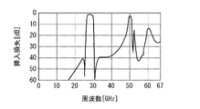
図12は、本実施の形態に係るバンドパスフィルタ1の挿入損失の周波数特性の一例を示している。図13は、第1の比較例のバンドパスフィルタの挿入損失の周波数特性の一例を示している。図12および図13に示した特性は、シミュレーションによって求めたものである。図12および図13において、横軸は周波数を示し、縦軸は挿入損失を示している。図12および図13に示した例では、バンドパスフィルタ1および第1の比較例のバンドパスフィルタの通過帯域は、約26〜30GHzであり、通過帯域の中心周波数は、約28GHzである。 FIG. 12 shows an example of the frequency characteristic of the insertion loss of the bandpass filter 1 according to the present embodiment. FIG. 13 shows an example of the frequency characteristic of the insertion loss of the bandpass filter of the first comparative example. The characteristics shown in FIGS. 12 and 13 were obtained by simulation. In FIGS. 12 and 13, the horizontal axis represents frequency and the vertical axis represents insertion loss. In the examples shown in FIGS. 12 and 13, the pass band of the bandpass filter 1 and the bandpass filter of the first comparative example is about 26 to 30 GHz, and the center frequency of the pass band is about 28 GHz.

シミュレーションにおけるバンドパスフィルタ1では、第1の仕切り部7の存在を前提として、図12に示したように第1の通過帯域近傍領域と第2の通過帯域近傍領域の両方に減衰極が生じるように、2つの飛び越し結合の大きさが調整されている。第1の通過帯域近傍領域は、約24〜26GHzの周波数領域である。第2の通過帯域近傍領域は、約30〜32GHzの周波数領域である。図13に示した第1の比較例のバンドパスフィルタの特性では、第1の通過帯域近傍領域には減衰極は無く、第2の通過帯域近傍領域における減衰極における挿入損失はバンドパスフィルタ1に比べて小さくなっている。これは、第1の比較例のバンドパスフィルタでは、第1の仕切り部7を除いたことにより、共振器51,55間の磁気結合の大きさが、バンドパスフィルタ1において調整された大きさからずれたためである。 In the bandpass filter 1 in the simulation, on the premise of the existence of the first partition portion 7, as shown in FIG. 12, an attenuation pole is generated in both the region near the first passband and the region near the second passband. In addition, the size of the two jump couplings has been adjusted. The region near the first pass band is a frequency region of about 24 to 26 GHz. The region near the second pass band is a frequency region of about 30 to 32 GHz. In the characteristics of the bandpass filter of the first comparative example shown in FIG. 13, there is no attenuation pole in the region near the first passband, and the insertion loss at the attenuation pole in the region near the second passband is the bandpass filter 1. It is smaller than. This is because in the bandpass filter of the first comparative example, the magnitude of the magnetic coupling between the resonators 51 and 55 is adjusted in the bandpass filter 1 by removing the first partition portion 7. This is because it deviated from.

また、図13に示した第1の比較例のバンドパスフィルタの特性では、約40GHzにおいて挿入損失が極端に小さくなるピークが存在している。これは、約40GHzにおいて最低次導波管モードによる不要な共振が生じているためと考えられる。図12に示したバンドパスフィルタ1の特性では、図13に示した特性において生じているようなピークは存在せず、図13に示した特性に比べて、通過帯域よりも高い周波数領域における減衰特性は良好である。 Further, in the characteristics of the bandpass filter of the first comparative example shown in FIG. 13, there is a peak in which the insertion loss becomes extremely small at about 40 GHz. It is considered that this is because unnecessary resonance occurs in the lowest-order waveguide mode at about 40 GHz. In the characteristics of the bandpass filter 1 shown in FIG. 12, there is no peak as generated in the characteristics shown in FIG. 13, and the attenuation in the frequency region higher than the pass band is compared with the characteristics shown in FIG. The characteristics are good.

また、図12に示したバンドパスフィルタ1の特性では、約55GHzにおける挿入損失が大きくなっている。これは、ノッチフィルタ部の作用によるものである。 Further, in the characteristics of the bandpass filter 1 shown in FIG. 12, the insertion loss at about 55 GHz is large. This is due to the action of the notch filter unit.

図12から、本実施の形態に係るバンドパスフィルタ1によれば、第1の通過帯域近傍領域と第2の通過帯域近傍領域の両方において挿入損失が急峻に変化し、且つ最低次導波管モードに起因した減衰特性の悪化が抑制された良好な特性を実現できることが分かる。 From FIG. 12, according to the bandpass filter 1 according to the present embodiment, the insertion loss changes sharply in both the region near the first passband and the region near the second passband, and the lowest-order waveguide It can be seen that good characteristics can be realized in which deterioration of damping characteristics due to the mode is suppressed.

[第2の実施の形態]
次に、本発明の第2の実施の形態について説明する。始めに、図14および図15を参照して、本実施の形態に係るバンドパスフィルタの構成について説明する。図14は、本実施の形態に係るバンドパスフィルタの構造を示す斜視図である。図15は、本実施の形態に係るバンドパスフィルタの回路構成を示す回路図である。
[Second Embodiment]
Next, a second embodiment of the present invention will be described. First, the configuration of the bandpass filter according to the present embodiment will be described with reference to FIGS. 14 and 15. FIG. 14 is a perspective view showing the structure of the bandpass filter according to the present embodiment. FIG. 15 is a circuit diagram showing a circuit configuration of a bandpass filter according to the present embodiment.

本実施の形態に係るバンドパスフィルタ100は、本体2と、第1の入出力ポート3および第2の入出力ポート4と、3つ以上の共振器と、シールド6と、仕切り部107と、結合調整部108とを備えている。本体2は、積層体20を含んでいる。 The bandpass filter 100 according to the present embodiment includes a main body 2, a first input / output port 3, a second input / output port 4, three or more resonators, a shield 6, a partition portion 107, and the like. It is provided with a coupling adjusting unit 108. The main body 2 includes the laminated body 20.

3つ以上の共振器は、回路構成上、第1の入出力ポート3と第2の入出力ポート4の間に設けられている。本実施の形態では、3つ以上の共振器は、6つの共振器151,152,153,154,155,156である。6つの共振器151,152,153,154,155,156は、回路構成上、第1の入出力ポート3側からこの順に配置されている。6つの共振器151〜156は、回路構成上隣接する2つの共振器が電磁結合するように構成されている。具体的に説明すると、共振器151〜156は、共振器151,152が回路構成上隣接して電磁結合し、共振器152,153が回路構成上隣接して電磁結合し、共振器153,154が回路構成上隣接して電磁結合し、共振器154,155が回路構成上隣接して電磁結合し、共振器155,156が回路構成上隣接して電磁結合するように構成されている。また、本実施の形態では特に、回路構成上隣接する2つの共振器の間の電磁結合は、容量結合である。また、本実施の形態では特に、共振器151〜156の各々は、両端開放型共振器であり且つ1/2波長共振器である。 Three or more resonators are provided between the first input / output port 3 and the second input / output port 4 in terms of circuit configuration. In this embodiment, the three or more resonators are six resonators 151,152,153,154,155,156. The six resonators 151, 152, 153, 154, 155, 156 are arranged in this order from the first input / output port 3 side in the circuit configuration. The six resonators 151 to 156 are configured such that two adjacent resonators are electromagnetically coupled in terms of circuit configuration. Specifically, in the resonators 151 to 156, the resonators 151 and 152 are electromagnetically coupled adjacent to each other in terms of circuit configuration, and the resonators 152 and 153 are electromagnetically coupled adjacent to each other in terms of circuit configuration, and the resonators 153 and 154 are electromagnetically coupled. Are electromagnetically coupled adjacent to each other in the circuit configuration, the resonators 154 and 155 are electromagnetically coupled adjacent to each other in the circuit configuration, and the resonators 155 and 156 are electromagnetically coupled adjacent to each other in the circuit configuration. Further, in the present embodiment, in particular, the electromagnetic coupling between two resonators adjacent to each other in the circuit configuration is a capacitive coupling. Further, in the present embodiment, in particular, each of the resonators 151 to 156 is an open-ended resonator and a 1/2 wavelength resonator.

シールド6の第1の部分61、第2の部分62および接続部63は、6つの共振器151〜156を囲むように配置されている。第1の部分61は、積層体20の主要部21の第1の端面21aに配置された第1の導体層1313によって構成されている。第2の部分62は、積層体20の主要部21の第2の端面21bに配置された第2の導体層1521によって構成されている。 The first portion 61, the second portion 62, and the connecting portion 63 of the shield 6 are arranged so as to surround the six resonators 151 to 156. The first portion 61 is composed of a first conductor layer 1313 arranged on the first end surface 21a of the main portion 21 of the laminated body 20. The second portion 62 is composed of a second conductor layer 1521 arranged on the second end surface 21b of the main portion 21 of the laminated body 20.

バンドパスフィルタ100は、共振器151,152間の容量結合を実現するキャパシタC112と、共振器152,153間の容量結合を実現するキャパシタC123と、共振器153,154間の容量結合を実現するキャパシタC134と、共振器154,155間の容量結合を実現するキャパシタC145と、共振器155,156間の容量結合を実現するキャパシタC156とを備えている。 The bandpass filter 100 realizes the capacitance coupling between the capacitor C112 which realizes the capacitance coupling between the resonators 151 and 152, the capacitor C123 which realizes the capacitance coupling between the resonators 152 and 153, and the resonators 153 and 154. It includes a capacitor C134, a capacitor C145 that realizes a capacitive coupling between the resonators 154 and 155, and a capacitor C156 that realizes a capacitive coupling between the resonators 155 and 156.

本実施の形態では、6つの共振器151〜156のうち回路構成上第1の入出力ポート3に対して2番目に近い共振器152と、6つの共振器151〜156のうち回路構成上第2の入出力ポート4に対して2番目に近い共振器155は、回路構成上隣接していないが磁気結合している。共振器152は、本発明における第1の共振器に対応する。共振器155は、本発明における第2の共振器に対応する。 In the present embodiment, the resonator 152, which is the second closest to the first input / output port 3 in the circuit configuration among the six resonators 151 to 156, and the first of the six resonators 151 to 156 in terms of the circuit configuration. The resonator 155, which is the second closest to the input / output port 4 of 2, is not adjacent in the circuit configuration, but is magnetically coupled. The resonator 152 corresponds to the first resonator in the present invention. The resonator 155 corresponds to the second resonator in the present invention.

また、本実施の形態では、6つの共振器151〜156のうち回路構成上第1の入出力ポート3に最も近い共振器151と、6つの共振器151〜156のうち回路構成上第2の入出力ポート4に最も近い共振器156は、回路構成上隣接していないが容量結合している。図15において、符号C116を付したキャパシタの記号は、共振器151,156間の容量結合を表している。 Further, in the present embodiment, the resonator 151, which is the closest to the first input / output port 3 in the circuit configuration among the six resonators 151 to 156, and the second of the six resonators 151 to 156 in terms of the circuit configuration. The resonator 156 closest to the input / output port 4 is not adjacent in the circuit configuration, but is capacitively coupled. In FIG. 15, the symbol of the capacitor with the reference numeral C116 represents the capacitive coupling between the resonators 151 and 156.

バンドパスフィルタ100は、更に、第1の入出力ポート3と共振器151との間に設けられたキャパシタC101と、第2の入出力ポート4と共振器156との間に設けられたキャパシタC102とを備えている。 The bandpass filter 100 further includes a capacitor C101 provided between the first input / output port 3 and the resonator 151, and a capacitor C102 provided between the second input / output port 4 and the resonator 156. And have.

バンドパスフィルタ100は、更に、第1の実施の形態と同様に、2つの線路91,92を備えている。 The bandpass filter 100 further includes two lines 91 and 92, as in the first embodiment.

共振器151は、導体よりなる共振器導体部1510を有している。共振器152は、導体よりなる共振器導体部1520を有している。共振器153は、導体よりなる共振器導体部1530を有している。共振器154は、導体よりなる共振器導体部1540を有している。共振器155は、導体よりなる共振器導体部1550を有している。共振器156は、導体よりなる共振器導体部1560を有している。共振器導体部1520は、本発明における第1の共振器導体部に対応する。共振器導体部1550は、本発明における第2の共振器導体部に対応する。 The resonator 151 has a resonator conductor portion 1510 made of a conductor. The resonator 152 has a resonator conductor portion 1520 made of a conductor. The resonator 153 has a resonator conductor portion 1530 made of a conductor. The resonator 154 has a resonator conductor portion 1540 made of a conductor. The resonator 155 has a resonator conductor portion 1550 made of a conductor. The resonator 156 has a resonator conductor portion 1560 made of a conductor. The resonator conductor portion 1520 corresponds to the first resonator conductor portion in the present invention. The resonator conductor portion 1550 corresponds to the second resonator conductor portion in the present invention.

共振器導体部1510,1520,1530,1540,1550,1560の各々は、第1の方向すなわちZ方向と交差する方向に延びている。本実施の形態では特に、共振器導体部1510,1520,1530,1540,1550,1560の各々は、第1の方向すなわちZ方向に直交する方向に延びている。 Each of the resonator conductor portions 1510, 1520, 1530, 1540, 1550, and 1560 extends in the first direction, that is, in the direction intersecting the Z direction. In this embodiment, in particular, each of the resonator conductor portions 1510, 1520, 1530, 1540, 1550, and 1560 extends in the first direction, that is, in the direction orthogonal to the Z direction.

共振器導体部1510,1520,1530,1540,1550,1560の各々は、互いに反対側に位置する第1端と第2端を有している。前述のように、共振器151〜156の各々は、両端開放型共振器である。そのため、共振器導体部1510,1520,1530,1540,1550,1560の各々の第1端と第2端は、いずれも開放されている。共振器導体部1510,1520,1530,1540,1550,1560の各々は、バンドパスフィルタ100の通過帯域の中心周波数に対応する波長の1/2またはそれに近い長さを有している。 Each of the resonator conductor portions 1510, 1520, 1530, 1540, 1550, and 1560 has a first end and a second end located on opposite sides of each other. As described above, each of the resonators 151 to 156 is an open-ended resonator. Therefore, the first end and the second end of each of the resonator conductor portions 1510, 1520, 1530, 1540, 1550, and 1560 are open. Each of the resonator conductors 1510, 1520, 1530, 1540, 1550, and 1560 has a length of 1/2 or close to the wavelength corresponding to the center frequency of the pass band of the bandpass filter 100.

仕切り部107は、その少なくとも一部が共振器導体部1520と共振器導体部1550の間を通過するように延びて、第1の部分61と第2の部分62とに接している。本実施の形態では特に、仕切り部107は、第1の方向すなわちZ方向に延びている。また、仕切り部107は、第1の部分61と第2の部分62を最短経路で接続している。すなわち、仕切り部107のZ方向の長さは、第1の部分61と第2の部分62の間の距離と等しい。 At least a part of the partition portion 107 extends so as to pass between the resonator conductor portion 1520 and the resonator conductor portion 1550, and is in contact with the first portion 61 and the second portion 62. In particular, in the present embodiment, the partition portion 107 extends in the first direction, that is, the Z direction. Further, the partition portion 107 connects the first portion 61 and the second portion 62 by the shortest path. That is, the length of the partition portion 107 in the Z direction is equal to the distance between the first portion 61 and the second portion 62.

また、仕切り部107は、主要部21を構成する2つ以上の誘電体層を貫通している。本実施の形態では、仕切り部107は、それぞれ主要部21を構成する2つ以上の誘電体層を貫通する複数のスルーホール列107Tと、導体層107Cとを含んでいる。複数のスルーホール列107Tは、本発明における第1のスルーホール列に対応する。図14では、個々のスルーホール列107Tを円柱で表している。複数のスルーホール列107Tの各々は、直列に接続された2つ以上のスルーホールを含んでいる。複数のスルーホール列107Tの各々は、Z方向に延びている。また、複数のスルーホール列107Tは、Y方向に並ぶように配列されている。本実施の形態では、スルーホール列107Tの数は7である。 Further, the partition portion 107 penetrates two or more dielectric layers constituting the main portion 21. In the present embodiment, the partition portion 107 includes a plurality of through-hole rows 107T penetrating two or more dielectric layers constituting the main portion 21, and a conductor layer 107C. The plurality of through-hole rows 107T correspond to the first through-hole row in the present invention. In FIG. 14, each through-hole row 107T is represented by a cylinder. Each of the plurality of through-hole rows 107T includes two or more through-holes connected in series. Each of the plurality of through-hole rows 107T extends in the Z direction. Further, the plurality of through-hole rows 107T are arranged so as to be arranged in the Y direction. In this embodiment, the number of through-hole rows 107T is 7.

結合調整部108は、共振器151,156間の容量結合の大きさを調整するためのものである。結合調整部108は、それぞれ主要部21を構成する2つ以上の誘電体層を貫通する複数のスルーホール列108Tを含んでいる。図14では、個々のスルーホール列108Tを円柱で表している。複数のスルーホール列108Tの各々は、直列に接続された2つ以上のスルーホールを含んでいる。複数のスルーホール列108Tの各々は、Z方向に延びて、第1の部分61と第2の部分62とに接している。また、複数のスルーホール列108Tは、共振器導体部1510の第2端と共振器導体部1560の第2端の近傍において、Y方向に並ぶように配列されている。本実施の形態では、スルーホール列108Tの数は2である。 The coupling adjusting unit 108 is for adjusting the size of the capacitive coupling between the resonators 151 and 156. The coupling adjusting unit 108 includes a plurality of through-hole rows 108T penetrating two or more dielectric layers each constituting the main unit 21. In FIG. 14, each through-hole row 108T is represented by a cylinder. Each of the plurality of through-hole rows 108T includes two or more through-holes connected in series. Each of the plurality of through-hole rows 108T extends in the Z direction and is in contact with the first portion 61 and the second portion 62. Further, the plurality of through-hole rows 108T are arranged so as to be arranged in the Y direction in the vicinity of the second end of the resonator conductor portion 1510 and the second end of the resonator conductor portion 1560. In the present embodiment, the number of through-hole rows 108T is 2.

シールド6の接続部63は、それぞれ主要部21を構成する2つ以上の誘電体層を貫通する複数のスルーホール列163Tを含んでいる。複数のスルーホール列163Tは、本発明における第2のスルーホール列に対応する。図14では、個々のスルーホール列163Tを円柱で表している。図14において、7つのスルーホール列107Tと2つのスルーホール列108T以外の複数の円柱で表わされた複数のスルーホール列は、全てスルーホール列163Tである。複数のスルーホール列163Tの各々は、直列に接続された2つ以上のスルーホールを含んでいる。複数のスルーホール列163Tの各々は、Z方向に延びている。 The connection portion 63 of the shield 6 includes a plurality of through-hole rows 163T penetrating two or more dielectric layers each constituting the main portion 21. The plurality of through-hole rows 163T correspond to the second through-hole row in the present invention. In FIG. 14, each through-hole row 163T is represented by a cylinder. In FIG. 14, a plurality of through-hole rows represented by a plurality of cylinders other than the seven through-hole rows 107T and the two through-hole rows 108T are all through-hole rows 163T. Each of the plurality of through-hole rows 163T includes two or more through-holes connected in series. Each of the plurality of through-hole rows 163T extends in the Z direction.

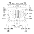
次に、図16ないし図24を参照して、本実施の形態における積層体20を構成する複数の誘電体層と、この複数の誘電体層に形成された複数の導体層および複数のスルーホールの構成の一例について説明する。この例では、積層体20は、積層された22層の誘電体層を有している。この22層の誘電体層を、下から順に1層目ないし22層目の誘電体層と呼ぶ。また、1層目ないし22層目の誘電体層を符号131〜152で表す。主要部21は、1層目ないし21層目の誘電体層131〜151によって構成されている。被覆部22は、22層目の誘電体層152によって構成されている。図16ないし図23において、複数の円は複数のスルーホールを表している。 Next, with reference to FIGS. 16 to 24, a plurality of dielectric layers constituting the laminate 20 in the present embodiment, a plurality of conductor layers formed in the plurality of dielectric layers, and a plurality of through holes. An example of the configuration of the above will be described. In this example, the laminated body 20 has 22 laminated dielectric layers. The 22 dielectric layers are referred to as the first to 22nd dielectric layers in this order from the bottom. Further, the first to 22nd dielectric layers are represented by reference numerals 131 to 152. The main portion 21 is composed of the first to 21st dielectric layers 131 to 151. The covering portion 22 is composed of the 22nd dielectric layer 152. In FIGS. 16 to 23, the plurality of circles represent a plurality of through holes.

図16は、1層目の誘電体層131のパターン形成面を示している。誘電体層131のパターン形成面には、第1の入出力ポート3を構成する導体層1311と、第2の入出力ポート4を構成する導体層1312と、シールド6の第1の部分61を構成する第1の導体層1313とが形成されている。 FIG. 16 shows the pattern forming surface of the first dielectric layer 131. On the pattern forming surface of the dielectric layer 131, a conductor layer 1311 forming the first input / output port 3, a conductor layer 1312 forming the second input / output port 4, and a first portion 61 of the shield 6 are provided. A first conductor layer 1313 and the constituent first conductor layer 1313 are formed.

また、誘電体層131には、導体層1311に接続されたスルーホール131T1と、導体層1312に接続されたスルーホール131T2とが形成されている。誘電体層131には、更に、7つのスルーホール列107Tの一部を構成する7つのスルーホール107T1と、2つのスルーホール列108Tの一部を構成する2つのスルーホール108T1と、複数のスルーホール列163Tの一部を構成する複数のスルーホール163T1が形成されている。図16において、スルーホール131T1,131T2,107T1,108T1以外の複数の円で表わされた複数のスルーホールは、全てスルーホール163T1である。スルーホール107T1,108T1,163T1は、第1の導体層1313に接続されている。 Further, the dielectric layer 131 is formed with a through hole 131T1 connected to the conductor layer 1311 and a through hole 131T2 connected to the conductor layer 1312. The dielectric layer 131 further includes seven through holes 107T1 forming a part of the seven through hole rows 107T, two through holes 108T1 forming a part of the two through hole rows 108T, and a plurality of through holes. A plurality of through holes 163T1 forming a part of the hole row 163T are formed. In FIG. 16, the plurality of through holes represented by the plurality of circles other than the through holes 131T1, 131T2, 107T1, 108T1 are all through holes 163T1. Through holes 107T1, 108T1, 163T1 are connected to the first conductor layer 1313.

図17は、2層目および3層目の誘電体層132,133のパターン形成面を示している。誘電体層132,133の各々には、スルーホール132T1,132T2が形成されている。2層目の誘電体層132に形成されたスルーホール132T1,132T2には、それぞれ、図16に示したスルーホール131T1,131T2が接続されている。 FIG. 17 shows the pattern forming surfaces of the second and third dielectric layers 132 and 133. Through holes 132T1 and 132T2 are formed in each of the dielectric layers 132 and 133. Through-holes 131T1 and 131T2 shown in FIG. 16 are connected to through-holes 132T1 and 132T2 formed in the second dielectric layer 132, respectively.

誘電体層132,133の各々には、更に、7つのスルーホール列107Tの一部を構成する7つのスルーホール107T2が形成されている。2層目の誘電体層132に形成された7つのスルーホール107T2には、図16に示した7つのスルーホール107T1が接続されている。 Seven through-holes 107T2 forming a part of the seven through-hole rows 107T are further formed in each of the dielectric layers 132 and 133. The seven through holes 107T1 shown in FIG. 16 are connected to the seven through holes 107T2 formed in the second dielectric layer 132.

誘電体層132,133の各々には、更に、2つのスルーホール列108Tの一部を構成する2つのスルーホール108T2が形成されている。2層目の誘電体層132に形成された2つのスルーホール108T2には、図16に示した2つのスルーホール108Tが接続されている。 Each of the dielectric layers 132 and 133 is further formed with two through-holes 108T2 forming a part of the two through-hole rows 108T. The two through holes 108T 1 shown in FIG. 16 are connected to the two through holes 108T2 formed in the second dielectric layer 132.

誘電体層132,133の各々には、更に、複数のスルーホール列163Tの一部を構成する複数のスルーホール163T2が形成されている。図17において、スルーホール132T1,132T2,107T2,108T2以外の複数の円で表わされた複数のスルーホールは、全てスルーホール163T2である。2層目の誘電体層132に形成された複数のスルーホール163T2には、図16に示した複数のスルーホール163T1が接続されている。 Each of the dielectric layers 132 and 133 is further formed with a plurality of through holes 163T2 forming a part of the plurality of through hole rows 163T. In FIG. 17, the plurality of through holes represented by the plurality of circles other than the through holes 132T1, 132T2, 107T2, 108T2 are all through holes 163T2. The plurality of through holes 163T1 shown in FIG. 16 are connected to the plurality of through holes 163T2 formed in the second dielectric layer 132.

誘電体層132,133では、上下に隣接する同じ符号のスルーホール同士が互いに接続されている。 In the dielectric layers 132 and 133, through holes having the same reference numerals vertically adjacent to each other are connected to each other.

図18は、4層目の誘電体層134のパターン形成面を示している。誘電体層134のパターン形成面には、線路91を構成する導体層1341と、線路92を構成する導体層1342が形成されている。導体層1341,1342の各々は、互いに反対側に位置する第1端と第2端を有している。導体層1341における第1端の近傍部分には、3層目の誘電体層133に形成されたスルーホール132T1が接続されている。導体層1342における第1端の近傍部分には、3層目の誘電体層133に形成されたスルーホール132T2が接続されている。導体層1341における第2端の近傍の一部と、導体層1342における第2端の近傍の一部は、誘電体層131,132,133を介して、図16に示した導体層1313に対向している。 FIG. 18 shows the pattern forming surface of the fourth dielectric layer 134. A conductor layer 1341 forming the line 91 and a conductor layer 1342 forming the line 92 are formed on the pattern forming surface of the dielectric layer 134. Each of the conductor layers 1341, 1342 has a first end and a second end located on opposite sides of each other. A through hole 132T1 formed in the third dielectric layer 133 is connected to a portion of the conductor layer 1341 near the first end. Through holes 132T2 formed in the third dielectric layer 133 are connected to the portion near the first end of the conductor layer 1342. A part of the vicinity of the second end of the conductor layer 1341 and a part of the vicinity of the second end of the conductor layer 1342 face the conductor layer 1313 shown in FIG. 16 via the dielectric layers 131, 132, 133. doing.

また、誘電体層134には、導体層1341における第1端の近傍部分に接続されたスルーホール134T1と、導体層1342における第1端の近傍部分に接続されたスルーホール134T2とが形成されている。 Further, the dielectric layer 134 is formed with a through hole 134T1 connected to a portion near the first end of the conductor layer 1341 and a through hole 134T2 connected to a portion near the first end of the conductor layer 1342. There is.

誘電体層134には、更に、7つのスルーホール列107Tの一部を構成する7つのスルーホール107T4が形成されている。7つのスルーホール107T4には、3層目の誘電体層133に形成された7つのスルーホール107T2が接続されている。 The dielectric layer 134 is further formed with seven through-holes 107T4 forming a part of the seven through-hole rows 107T. The seven through holes 107T4 are connected to the seven through holes 107T2 formed in the third dielectric layer 133.

誘電体層134には、更に、2つのスルーホール列108Tの一部を構成する2つのスルーホール108T4が形成されている。2つのスルーホール108T4には、3層目の誘電体層133に形成された2つのスルーホール108T2が接続されている。 The dielectric layer 134 is further formed with two through-holes 108T4 forming a part of the two through-hole rows 108T. Two through holes 108T2 formed in the third dielectric layer 133 are connected to the two through holes 108T4.

誘電体層134には、更に、複数のスルーホール列163Tの一部を構成する複数のスルーホール163T4が形成されている。図18において、スルーホール134T1,134T2,107T4,108T4以外の複数の円で表わされた複数のスルーホールは、全てスルーホール163T4である。複数のスルーホール163T4には、3層目の誘電体層133に形成された複数のスルーホール163T2が接続されている。 The dielectric layer 134 is further formed with a plurality of through holes 163T4 forming a part of the plurality of through hole rows 163T. In FIG. 18, the plurality of through holes represented by the plurality of circles other than the through holes 134T1, 134T2, 107T4, 108T4 are all through holes 163T4. A plurality of through holes 163T2 formed in the third dielectric layer 133 are connected to the plurality of through holes 163T4.

図19は、5層目ないし9層目の誘電体層135〜139のパターン形成面を示している。誘電体層135〜139の各々には、スルーホール135T1,135T2が形成されている。5層目の誘電体層135に形成されたスルーホール135T1,135T2には、それぞれ、図18に示したスルーホール134T1,134T2が接続されている。 FIG. 19 shows the pattern forming surface of the fifth to ninth dielectric layers 135 to 139. Through holes 135T1 and 135T2 are formed in each of the dielectric layers 135 to 139. Through-holes 134T1 and 134T2 shown in FIG. 18 are connected to through-holes 135T1 and 135T2 formed in the fifth dielectric layer 135, respectively.

誘電体層135〜139の各々には、更に、7つのスルーホール列107Tの一部を構成する7つのスルーホール107T5が形成されている。5層目の誘電体層135に形成された7つのスルーホール107T5には、図18に示した7つのスルーホール107T4が接続されている。 Each of the dielectric layers 135 to 139 is further formed with seven through holes 107 T5 forming a part of the seven through hole rows 107 T. The seven through holes 107T4 shown in FIG. 18 are connected to the seven through holes 107T5 formed in the fifth dielectric layer 135.

誘電体層135〜139の各々には、更に、2つのスルーホール列108Tの一部を構成する2つのスルーホール108T5が形成されている。5層目の誘電体層135に形成された2つのスルーホール108T5には、図18に示した2つのスルーホール108T4が接続されている。 Each of the dielectric layers 135 to 139 is further formed with two through holes 108T5 forming a part of the two through hole rows 108T. The two through holes 108T4 shown in FIG. 18 are connected to the two through holes 108T5 formed in the fifth dielectric layer 135.

誘電体層135〜139の各々には、更に、複数のスルーホール列163Tの一部を構成する複数のスルーホール163T5が形成されている。図19において、スルーホール135T1,135T2,107T5,108T5以外の複数の円で表わされた複数のスルーホールは、全てスルーホール163T5である。5層目の誘電体層135に形成された複数のスルーホール163T5には、図18に示した複数のスルーホール163T4が接続されている。 Each of the dielectric layers 135 to 139 is further formed with a plurality of through holes 163T5 forming a part of the plurality of through hole rows 163T. In FIG. 19, the plurality of through holes represented by the plurality of circles other than the through holes 135T1, 135T2, 107T5, and 108T5 are all through holes 163T5. The plurality of through holes 163T4 shown in FIG. 18 are connected to the plurality of through holes 163T5 formed in the fifth dielectric layer 135.

誘電体層135〜139では、上下に隣接する同じ符号のスルーホール同士が互いに接続されている。 In the dielectric layers 135 to 139, through holes having the same reference numerals vertically adjacent to each other are connected to each other.

図20は、10層目の誘電体層140のパターン形成面を示している。誘電体層140のパターン形成面には、図15に示したキャパシタC101を構成するための導体層1401と、図15に示したキャパシタC102を構成するための導体層1402とが形成されている。導体層1401には、9層目の誘電体層139に形成されたスルーホール135T1が接続されている。導体層1402には、9層目の誘電体層139に形成されたスルーホール135T2が接続されている。 FIG. 20 shows the pattern forming surface of the 10th dielectric layer 140. On the pattern forming surface of the dielectric layer 140, a conductor layer 1401 for forming the capacitor C101 shown in FIG. 15 and a conductor layer 1402 for forming the capacitor C102 shown in FIG. 15 are formed. Through holes 135T1 formed in the ninth dielectric layer 139 are connected to the conductor layer 1401. Through holes 135T2 formed in the ninth dielectric layer 139 are connected to the conductor layer 1402.

誘電体層140のパターン形成面には、更に、それぞれ図15に示したキャパシタC112,C123,C134,C145,C156を構成するための導体層1403,1404,1405,1406,1407が形成されている。 Further, conductor layers 1403, 1404, 1405, 1406, 1407 for forming the capacitors C112, C123, C134, C145, and C156 shown in FIG. 15 are further formed on the pattern forming surface of the dielectric layer 140. ..

また、誘電体層140には、7つのスルーホール列107Tの一部を構成する7つのスルーホール107T10が形成されている。7つのスルーホール107T10には、9層目の誘電体層139に形成された7つのスルーホール107T5が接続されている。 Further, the dielectric layer 140 is formed with seven through-holes 107T10 forming a part of the seven through-hole rows 107T. Seven through holes 107T5 formed in the ninth dielectric layer 139 are connected to the seven through holes 107T10.

誘電体層140には、更に、2つのスルーホール列108Tの一部を構成する2つのスルーホール108T10が形成されている。2つのスルーホール108T10には、9層目の誘電体層139に形成された2つのスルーホール108T5が接続されている。 The dielectric layer 140 is further formed with two through-holes 108T10 forming a part of the two through-hole rows 108T. Two through holes 108T5 formed in the ninth dielectric layer 139 are connected to the two through holes 108T10.

誘電体層140には、更に、複数のスルーホール列163Tの一部を構成する複数のスルーホール163T10が形成されている。図20において、スルーホール107T10,108T10以外の複数の円で表わされた複数のスルーホールは、全てスルーホール163T10である。複数のスルーホール163T10には、9層目の誘電体層139に形成された複数のスルーホール163T5が接続されている。 The dielectric layer 140 is further formed with a plurality of through holes 163T10 forming a part of the plurality of through hole rows 163T. In FIG. 20, the plurality of through holes represented by the plurality of circles other than the through holes 107T10 and 108T10 are all through holes 163T 10 . A plurality of through holes 163T5 formed in the ninth dielectric layer 139 are connected to the plurality of through holes 163T10.

図21は、11層目の誘電体層141のパターン形成面を示している。誘電体層141には、7つのスルーホール列107Tの一部を構成する7つのスルーホール107T11が形成されている。7つのスルーホール107T11には、図20に示した7つのスルーホール107T10が接続されている。 FIG. 21 shows the pattern forming surface of the eleventh dielectric layer 141. The dielectric layer 141 is formed with seven through-holes 107T 11 forming a part of the seven through-hole rows 107T. The seven through holes 107T10 shown in FIG. 20 are connected to the seven through holes 107T11.

誘電体層141には、更に、2つのスルーホール列108Tの一部を構成する2つのスルーホール108T11が形成されている。2つのスルーホール108T11には、図20に示した2つのスルーホール108T10が接続されている。 The dielectric layer 141 is further formed with two through-holes 108T11 forming a part of the two through-hole rows 108T. The two through holes 108T10 shown in FIG. 20 are connected to the two through holes 108T11.

誘電体層141には、更に、複数のスルーホール列163Tの一部を構成する複数のスルーホール163T11が形成されている。図21において、スルーホール107T11,108T11以外の複数の円で表わされた複数のスルーホールは、全てスルーホール163T11である。複数のスルーホール163T11には、図20に示した複数のスルーホール163T10が接続されている。 The dielectric layer 141 is further formed with a plurality of through holes 163T11 forming a part of the plurality of through hole rows 163T. In FIG. 21, the plurality of through holes represented by the plurality of circles other than the through holes 107T11 and 108T11 are all through holes 163T11. The plurality of through holes 163T10 shown in FIG. 20 are connected to the plurality of through holes 163T11.

図22は、12層目の誘電体層142のパターン形成面を示している。誘電体層142のパターン形成面には、共振器導体部1510,1520,1530,1540,1550,1560が形成されている。 FIG. 22 shows the pattern forming surface of the twelfth dielectric layer 142. Resonator conductor portions 1510, 1520, 1530, 1540, 1550, and 1560 are formed on the pattern forming surface of the dielectric layer 142.

共振器導体部1510は、互いに反対側に位置する第1端1510aと第2端1510bを有している。共振器導体部1520は、互いに反対側に位置する第1端1520aと第2端1520bを有している。共振器導体部1530は、互いに反対側に位置する第1端1530aと第2端1530bを有している。共振器導体部1540は、互いに反対側に位置する第1端1540aと第2端1540bを有している。共振器導体部1550は、互いに反対側に位置する第1端1550aと第2端1550bを有している。共振器導体部1560は、互いに反対側に位置する第1端1560aと第2端1560bを有している。 The resonator conductor portion 1510 has a first end 1510a and a second end 1510b located on opposite sides of each other. The resonator conductor portion 1520 has a first end 1520a and a second end 1520b located on opposite sides of each other. The resonator conductor portion 1530 has a first end 1530a and a second end 1530b located on opposite sides of each other. The resonator conductor portion 1540 has a first end 1540a and a second end 1540b located on opposite sides of each other. The resonator conductor portion 1550 has a first end 1550a and a second end 1550b located on opposite sides of each other. The resonator conductor portion 1560 has a first end 1560a and a second end 1560b located on opposite sides of each other.

共振器導体部1510,1560の各々は、X方向に延びている。また、共振器導体部1510,1560は、それらと交差してX方向に延びる1つの直線が存在する位置関係で配置されている。共振器導体部1510の第2端1510bと共振器導体部1560の第2端1560bは、所定の間隔を開けて隣接している。第2端1510bと第2端1560bの間隔は、共振器導体部1510,1560の各々の長さよりも十分に小さい。 Each of the resonator conductor portions 1510 and 1560 extends in the X direction. Further, the resonator conductor portions 1510 and 1560 are arranged in a positional relationship in which one straight line intersecting them and extending in the X direction exists. The second end 1510b of the resonator conductor portion 1510 and the second end 1560b of the resonator conductor portion 1560 are adjacent to each other with a predetermined interval. The distance between the second end 1510b and the second end 1560b is sufficiently smaller than the respective lengths of the resonator conductor portions 1510 and 1560.

共振器導体部1520,1550の各々は、Y方向に延びている。また、共振器導体部1520,1550は、所定の間隔を開けてX方向に隣接している。共振器導体部1520,1550の間隔は、共振器導体部1520,1550の各々の長さよりも小さい。 Each of the resonator conductor portions 1520 and 1550 extends in the Y direction. Further, the resonator conductor portions 1520 and 1550 are adjacent to each other in the X direction with a predetermined interval. The distance between the resonator conductors 1520 and 1550 is smaller than the lengths of the resonator conductors 1520 and 1550, respectively.

共振器導体部1520の第1端1520aは、共振器導体部1510の第2端1510bの近傍に配置されている。共振器導体部1550の第1端1550aは、共振器導体部1560の第2端1560bの近傍に配置されている。 The first end 1520a of the resonator conductor portion 1520 is arranged in the vicinity of the second end 1510b of the resonator conductor portion 1510. The first end 1550a of the resonator conductor portion 1550 is arranged in the vicinity of the second end 1560b of the resonator conductor portion 1560.

共振器導体部1530は、第1の部分1530Aと第2の部分1530Bと第3の部分1530Cを含んでいる。第1の部分1530Aは第1端1530aを有し、第2の部分1530Bは第2端1530bを有している。第1の部分1530AはX方向に延び、第2の部分1530BはY方向に延びている。第3の部分1530Cは、第1の部分1530Aにおける第1端1530aとは反対側の端部と、第2の部分1530Bにおける第2端1530bとは反対側の端部と接続している。図22では、第1の部分1530Aと第3の部分1530Cの境界と、第2の部分1530Bと第3の部分1530Cの境界を、破線で示している。第1端1530aは、共振器導体部1520の第2端1520bの近傍に配置されている。 The resonator conductor portion 1530 includes a first portion 1530A, a second portion 1530B, and a third portion 1530C. The first portion 1530A has a first end 1530a and the second portion 1530B has a second end 1530b. The first portion 1530A extends in the X direction and the second portion 1530B extends in the Y direction. The third portion 1530C is connected to the end of the first portion 1530A opposite to the first end 1530a and the end of the second portion 1530B opposite to the second end 1530b. In FIG. 22, the boundary between the first portion 1530A and the third portion 1530C and the boundary between the second portion 1530B and the third portion 1530C are shown by broken lines. The first end 1530a is arranged in the vicinity of the second end 1520b of the resonator conductor portion 1520.

共振器導体部1540は、第1の部分1540Aと第2の部分1540Bと第3の部分1540Cを含んでいる。第1の部分1540Aは第1端1540aを有し、第2の部分1540Bは第2端1540bを有している。第1の部分1540AはX方向に延び、第2の部分1540BはY方向に延びている。第3の部分1540Cは、第1の部分1540Aにおける第1端1540aとは反対側の端部と、第2の部分1540Bにおける第2端1540bとは反対側の端部と接続している。図22では、第1の部分1540Aと第3の部分1540Cの境界と、第2の部分1540Bと第3の部分1540Cの境界を、破線で示している。第1端1540aは、共振器導体部1550の第2端1550bの近傍に配置されている。 The resonator conductor portion 1540 includes a first portion 1540A, a second portion 1540B, and a third portion 1540C. The first portion 1540A has a first end 1540a and the second portion 1540B has a second end 1540b. The first portion 1540A extends in the X direction and the second portion 1540B extends in the Y direction. The third portion 1540C is connected to the end of the first portion 1540A opposite to the first end 1540a and the end of the second portion 1540B opposite to the second end 1540b. In FIG. 22, the boundary between the first portion 1540A and the third portion 1540C and the boundary between the second portion 1540B and the third portion 1540C are shown by broken lines. The first end 1540a is arranged in the vicinity of the second end 1550b of the resonator conductor portion 1550.

共振器導体部1530の第1端1530aと共振器導体部1540の第1端1540aは、所定の間隔を開けて隣接している。 The first end 1530a of the resonator conductor portion 1530 and the first end 1540a of the resonator conductor portion 1540 are adjacent to each other with a predetermined interval.

誘電体層142のパターン形成面には、更に、仕切り部107の一部を構成する導体層107Cが形成されている。導体層107Cは、共振器導体部1520と共振器導体部1550の間に位置して、Y方向に延びている。 A conductor layer 107C forming a part of the partition portion 107 is further formed on the pattern forming surface of the dielectric layer 142. The conductor layer 107C is located between the resonator conductor portion 1520 and the resonator conductor portion 1550 and extends in the Y direction.

また、誘電体層142には、7つのスルーホール列107Tの一部を構成する7つのスルーホール107T12が形成されている。7つのスルーホール107T12は、導体層107Cに接続されている。また、7つのスルーホール107T12には、図21に示した7つのスルーホール107T11が接続されている。 Further, the dielectric layer 142 is formed with seven through-holes 107T12 forming a part of the seven through-hole rows 107T. The seven through holes 107T12 are connected to the conductor layer 107C. Further, the seven through holes 107 T11 shown in FIG. 21 are connected to the seven through holes 107 T12.

誘電体層142には、更に、2つのスルーホール列108Tの一部を構成する2つのスルーホール108T12が形成されている。2つのスルーホール108T12には、図21に示した2つのスルーホール108T11が接続されている。 The dielectric layer 142 is further formed with two through-holes 108T12 forming a part of the two through-hole rows 108T. The two through holes 108T 11 shown in FIG. 21 are connected to the two through holes 108T 12.

誘電体層142には、更に、複数のスルーホール列163Tの一部を構成する複数のスルーホール163T12が形成されている。図22において、スルーホール107T12,108T12以外の複数の円で表わされた複数のスルーホールは、全てスルーホール163T12である。複数のスルーホール163T12には、図21に示した複数のスルーホール163T11が接続されている。 The dielectric layer 142 is further formed with a plurality of through holes 163T12 forming a part of the plurality of through hole rows 163T. In FIG. 22, the plurality of through holes represented by the plurality of circles other than the through holes 107T12 and 108T12 are all through holes 163T12. The plurality of through holes 163T11 shown in FIG. 21 are connected to the plurality of through holes 163T12.

図23は、13層目ないし21層目の誘電体層143〜151のパターン形成面を示している。誘電体層143〜151の各々には、7つのスルーホール列107Tの一部を構成する7つのスルーホール107T13が形成されている。13層目の誘電体層143に形成された7つのスルーホール107T13には、図22に示した7つのスルーホール107T12が接続されている。 FIG. 23 shows the pattern forming surfaces of the dielectric layers 143 to 151 of the 13th to 21st layers. Seven through-holes 107T 13 forming a part of the seven through-hole rows 107T are formed in each of the dielectric layers 143 to 151. The seven through holes 107T12 shown in FIG. 22 are connected to the seven through holes 107T13 formed in the dielectric layer 143 of the thirteenth layer.

誘電体層143〜151の各々には、更に、2つのスルーホール列108Tの一部を構成する2つのスルーホール108T13が形成されている。13層目の誘電体層143に形成された2つのスルーホール108T13には、図22に示した2つのスルーホール108T12が接続されている。 Each of the dielectric layers 143 to 151 is further formed with two through-holes 108T13 forming a part of the two through-hole rows 108T. The two through holes 108T12 shown in FIG. 22 are connected to the two through holes 108T13 formed in the dielectric layer 143 of the thirteenth layer.

誘電体層143〜151の各々には、更に、複数のスルーホール列163Tの一部を構成する複数のスルーホール163T13が形成されている。図23において、スルーホール107T13,108T13以外の複数の円で表わされた複数のスルーホールは、全てスルーホール163T13である。13層目の誘電体層143に形成された複数のスルーホール163T13には、図22に示した複数のスルーホール163T12が接続されている。 Each of the dielectric layers 143 to 151 is further formed with a plurality of through holes 163T13 forming a part of the plurality of through hole rows 163T. In FIG. 23, the plurality of through holes represented by the plurality of circles other than the through holes 107T13 and 108T13 are all through holes 163T13. The plurality of through holes 163T12 shown in FIG. 22 are connected to the plurality of through holes 163T13 formed in the dielectric layer 143 of the thirteenth layer.

誘電体層143〜151では、上下に隣接する同じ符号のスルーホール同士が互いに接続されている。 In the dielectric layers 143 to 151, through holes having the same reference numerals vertically adjacent to each other are connected to each other.

図24は、22層目の誘電体層152のパターン形成面を示している。誘電体層152のパターン形成面には、シールド6の第2の部分62を構成する第2の導体層1521が形成されている。第2の導体層1521には、21層目の誘電体層151に形成されたスルーホール107T13,108T13,163T13が接続されている。 FIG. 24 shows the pattern forming surface of the 22nd dielectric layer 152. A second conductor layer 1521 forming a second portion 62 of the shield 6 is formed on the pattern forming surface of the dielectric layer 152. Through holes 107T13, 108T13, and 163T13 formed in the dielectric layer 151 of the 21st layer are connected to the second conductor layer 1521.

本実施の形態に係るバンドパスフィルタ100は、1層目の誘電体層131のパターン形成面が本体2の第1の端面2Aになるように、1層目ないし22層目の誘電体層131〜152が積層されて構成される。22層目の誘電体層152におけるパターン形成面とは反対側の面は、本体2の第2の端面2Bになる。1層目ないし22層目の誘電体層131〜152は、積層体20を構成する。 In the bandpass filter 100 according to the present embodiment, the first to 22nd dielectric layers 131 so that the pattern forming surface of the first dielectric layer 131 becomes the first end surface 2A of the main body 2. ~ 152 are laminated and configured. The surface of the 22nd dielectric layer 152 opposite to the pattern forming surface is the second end surface 2B of the main body 2. The first to 22nd dielectric layers 131 to 152 constitute the laminated body 20.

共振器151〜156のそれぞれの共振器導体部1510,1520,1530,1540,1550,1560は、第1の方向すなわちZ方向に関して、積層体20内の同じ位置に配置されている。 The resonator conductor portions 1510, 1520, 1530, 1540, 1550, and 1560 of the resonators 151 to 156 are arranged at the same position in the laminate 20 with respect to the first direction, that is, the Z direction.

第1の入出力ポート3を構成する導体層1311は、スルーホール131T1,132T1,134T1,135T1を介して、図20に示した導体層1401に接続されている。導体層1401は、誘電体層140,141を介して、図22に示した共振器導体部1510における第1端1510aの近傍部分に対向している。図15に示したキャパシタC101は、導体層1401と共振器導体部1510と、これらの間の誘電体層140,141とによって構成されている。 The conductor layer 1311 constituting the first input / output port 3 is connected to the conductor layer 1401 shown in FIG. 20 via through holes 131T1, 132T1, 134T1, 135T1. The conductor layer 1401 faces the portion near the first end 1510a of the resonator conductor portion 1510 shown in FIG. 22 via the dielectric layers 140 and 141. The capacitor C101 shown in FIG. 15 is composed of a conductor layer 1401, a resonator conductor portion 1510, and dielectric layers 140 and 141 between them.

第2の入出力ポート4を構成する導体層1312は、スルーホール131T2,132T2,134T2,135T2を介して、図20に示した導体層1402に接続されている。導体層1402は、誘電体層140,141を介して、図22に示した共振器導体部1560における第1端1560aの近傍部分に対向している。図15に示したキャパシタC102は、導体層1402と共振器導体部1560と、これらの間の誘電体層140,141とによって構成されている。 The conductor layer 1312 constituting the second input / output port 4 is connected to the conductor layer 1402 shown in FIG. 20 via through holes 131T2, 132T2, 134T2, 135T2. The conductor layer 1402 faces the portion near the first end 1560a of the resonator conductor portion 1560 shown in FIG. 22 via the dielectric layers 140 and 141. The capacitor C102 shown in FIG. 15 is composed of a conductor layer 1402, a resonator conductor portion 1560, and dielectric layers 140 and 141 between them.

図20に示した導体層1403は、誘電体層140,141を介して、共振器導体部1510における第2端1510bの近傍部分と、共振器導体部1520における第1端1520aの近傍部分とに対向している。図15に示したキャパシタC112は、導体層1403と、共振器導体部1510,1520と、これらの間の誘電体層140,141とによって構成されている。 The conductor layer 1403 shown in FIG. 20 is formed in the vicinity of the second end 1510b of the resonator conductor portion 1510 and the vicinity of the first end 1520a of the resonator conductor portion 1520 via the dielectric layers 140 and 141. Facing each other. The capacitor C112 shown in FIG. 15 is composed of a conductor layer 1403, resonator conductor portions 1510 and 1520, and dielectric layers 140 and 141 between them.

図20に示した導体層1404は、誘電体層140,141を介して、共振器導体部1520における第2端1520bの近傍部分と、共振器導体部1530における第1端1530aの近傍部分とに対向している。図15に示したキャパシタC123は、導体層1404と、共振器導体部1520,1530と、これらの間の誘電体層140,141とによって構成されている。 The conductor layer 1404 shown in FIG. 20 is formed in the vicinity of the second end 1520b of the resonator conductor portion 1520 and the vicinity of the first end 1530a of the resonator conductor portion 1530 via the dielectric layers 140 and 141. Facing each other. The capacitor C123 shown in FIG. 15 is composed of a conductor layer 1404, resonator conductor portions 1520 and 1530, and dielectric layers 140 and 141 between them.

図20に示した導体層1405は、誘電体層140,141を介して、共振器導体部1530における第1端1530aの近傍部分と、共振器導体部1540における第1端1540aの近傍部分とに対向している。図15に示したキャパシタC134は、導体層1405と、共振器導体部1530,1540と、これらの間の誘電体層140,141とによって構成されている。 The conductor layer 1405 shown in FIG. 20 is formed in a portion near the first end 1530a in the resonator conductor portion 1530 and a portion near the first end 1540a in the resonator conductor portion 1540 via the dielectric layers 140 and 141. Facing each other. The capacitor C134 shown in FIG. 15 is composed of a conductor layer 1405, resonator conductor portions 1530 and 1540, and dielectric layers 140 and 141 between them.

図20に示した導体層1406は、誘電体層140,141を介して、共振器導体部1540における第1端1540aの近傍部分と、共振器導体部1550における第2端1550bの近傍部分とに対向している。図15に示したキャパシタC145は、導体層1406と、共振器導体部1540,1550と、これらの間の誘電体層140,141とによって構成されている。 The conductor layer 1406 shown in FIG. 20 is formed in a portion near the first end 1540a in the resonator conductor portion 1540 and a portion near the second end 1550b in the resonator conductor portion 1550 via the dielectric layers 140 and 141. Facing each other. The capacitor C145 shown in FIG. 15 is composed of a conductor layer 1406, resonator conductor portions 1540 and 1550, and dielectric layers 140 and 141 between them.

図20に示した導体層1407は、誘電体層140,141を介して、共振器導体部1550における第1端1550aの近傍部分と、共振器導体部1560における第2端1560bの近傍部分とに対向している。図15に示したキャパシタC156は、導体層1407と、共振器導体部1550,1560と、これらの間の誘電体層140,141とによって構成されている。 The conductor layer 1407 shown in FIG. 20 is formed in a portion near the first end 1550a in the resonator conductor portion 1550 and a portion near the second end 1560b in the resonator conductor portion 1560 via the dielectric layers 140 and 141. Facing each other. The capacitor C156 shown in FIG. 15 is composed of a conductor layer 1407, resonator conductor portions 1550 and 1560, and dielectric layers 140 and 141 between them.

仕切り部107の7つのスルーホール列107Tの各々は、スルーホール107T1,107T2,107T4,107T5,107T10,107T11,107T12,107T13が、Z方向に直列に接続されることによって構成されている。 Each of the seven through-hole rows 107T of the partition portion 107 is configured by connecting through-holes 107T1, 107T2, 107T4, 107T5, 107T10, 107T11, 107T12, 107T13 in series in the Z direction.

図16ないし図24に示した例では、仕切り部107は、共振器導体部1520と共振器導体部1550の間を通過するように延びて、第1の部分61と第2の部分62とに接している。 In the example shown in FIGS. 16 to 24, the partition portion 107 extends so as to pass between the resonator conductor portion 1520 and the resonator conductor portion 1550, and becomes a first portion 61 and a second portion 62. I'm in contact.

結合調整部108の2つのスルーホール列108Tの各々は、スルーホール108T1,108T2,108T4,108T5,108T10,108T11,108T12,108T13が、Z方向に直列に接続されることによって構成されている。 Each of the two through-hole rows 108T of the coupling adjusting unit 108 is configured by connecting the through-holes 108T1, 108T2, 108T4, 108T5, 108T10, 108T11, 108T12, 108T13 in series in the Z direction.

接続部163の複数のスルーホール列163Tの各々は、スルーホール163T1,163T2,163T4,163T5,163T10,163T11,163T12,163T13が、Z方向に直列に接続されることによって構成されている。
Each of the plurality of through-hole rows 163T of the connecting portion 163 is configured by connecting through-holes 163T1, 163T2, 163T4, 163T5, 163T10, 163T11, 163T12, 163T13 in series in the Z direction.

本実施の形態では、回路構成上隣接していない共振器152,155が磁気結合し、回路構成上隣接していない共振器151,156が容量結合している。共振器152と共振器151は回路構成上隣接し、且つ容量結合している。また、共振器155と共振器156は回路構成上隣接し、且つ容量結合している。このような回路構成上の関係を有する共振器151,152,155,156の共振器導体部1510,1520,1550,1560は、以下のような物理的な関係を有している。 In the present embodiment, the resonators 152 and 155 that are not adjacent in the circuit configuration are magnetically coupled, and the resonators 151 and 156 that are not adjacent in the circuit configuration are capacitively coupled. The resonator 152 and the resonator 151 are adjacent to each other in terms of circuit configuration and are capacitively coupled. Further, the resonator 155 and the resonator 156 are adjacent to each other in the circuit configuration and are capacitively coupled. The resonator conductor portions 1510, 1520, 1550, and 1560 of the resonators 151, 152, 155, and 156 having such a circuit configuration relationship have the following physical relationships.

共振器152,155のそれぞれの共振器導体部1520,1550は、他の共振器の共振器導体部を介することなく物理的に隣接している。本実施の形態では特に、いずれもY方向に延びる共振器導体部1520と共振器導体部1550が、それらの間に他の共振器の共振器導体部を介することなく、X方向に物理的に隣接している。これにより、共振器152,155間の磁気結合が実現されている。 The resonator conductor portions 1520 and 1550 of the resonators 152 and 155 are physically adjacent to each other without interposing the resonator conductor portions of the other resonators. In this embodiment, in particular, the resonator conductor portion 1520 and the resonator conductor portion 1550, both of which extend in the Y direction, physically extend in the X direction without interposing the resonator conductor portion of another resonator between them. Adjacent. As a result, magnetic coupling between the resonators 152 and 155 is realized.

また、共振器151,156のそれぞれの共振器導体部1510,1560は、他の共振器の共振器導体部を介することなく物理的に隣接している。本実施の形態では特に、共振器導体部1510の第2端1510bと、共振器導体部1560の第2端1560bが、それらの間に他の共振器の共振器導体部を介することなく、小さい間隔を開けて隣接している。これにより、共振器151,156間の容量結合が実現されている。 Further, the resonator conductor portions 1510 and 1560 of the resonators 151 and 156 are physically adjacent to each other without interposing the resonator conductor portions of other resonators. In this embodiment, in particular, the second end 1510b of the resonator conductor portion 1510 and the second end 1560b of the resonator conductor portion 1560 are small without interposing the resonator conductor portion of another resonator between them. Adjacent with a gap. As a result, capacitive coupling between the resonators 151 and 156 is realized.

また、共振器152,151のそれぞれの共振器導体部1520,1510は、他の共振器の共振器導体部を介することなく物理的に隣接している。これにより、共振器152,151間の容量結合を容易に実現することができる。 Further, the resonator conductor portions 1520 and 1510 of the resonators 152 and 151 are physically adjacent to each other without interposing the resonator conductor portions of other resonators. Thereby, the capacitive coupling between the resonators 152 and 151 can be easily realized.

また、共振器155,156のそれぞれの共振器導体部1550,1560は、他の共振器の共振器導体部を介することなく物理的に隣接している。これにより、共振器155,156間の容量結合を容易に実現することができる。 Further, the resonator conductor portions 1550 and 1560 of the resonators 155 and 156 are physically adjacent to each other without interposing the resonator conductor portions of other resonators. Thereby, the capacitive coupling between the resonators 155 and 156 can be easily realized.

次に、本実施の形態に係るバンドパスフィルタ100の作用および効果について説明する。バンドパスフィルタ100は、例えば、通過帯域が10〜30GHzの準ミリ波帯または30〜300GHzのミリ波帯に存在するように設計および構成される。 Next, the operation and effect of the bandpass filter 100 according to the present embodiment will be described. The bandpass filter 100 is designed and configured such that the pass band exists, for example, in the quasi-millimeter wave band of 10 to 30 GHz or the millimeter wave band of 30 to 300 GHz.

本実施の形態では、仕切り部107によって、シールド6で囲まれた空間が、共振器導体部1520が存在する空間と、共振器導体部1550が存在する空間とに仕切られる。これにより、本実施の形態によれば、第1の実施の形態と同様に、最低次導波管モードによって通過帯域よりも高い周波数領域における減衰特性が悪化することを防止することができる。 In the present embodiment, the space surrounded by the shield 6 is partitioned by the partition portion 107 into a space in which the resonator conductor portion 1520 exists and a space in which the resonator conductor portion 1550 exists. Thereby, according to the present embodiment, as in the first embodiment, it is possible to prevent the attenuation characteristic from being deteriorated in the frequency region higher than the pass band due to the lowest-order waveguide mode.

また、本実施の形態では、回路構成上隣接していない2段目の共振器152と5段目の共振器155が磁気結合している。共振器152,155間の磁気結合は、挿入損失の周波数特性において、通過帯域よりも低く通過帯域に近い周波数領域である第1の通過帯域近傍領域と、通過帯域よりも高く通過帯域に近い周波数領域である第2の通過帯域近傍領域の両方に、減衰極を生じさせることができる。 Further, in the present embodiment, the second-stage resonator 152 and the fifth-stage resonator 155, which are not adjacent to each other in the circuit configuration, are magnetically coupled. In the frequency characteristics of the insertion loss, the magnetic coupling between the resonators 152 and 155 is a frequency region near the first passband, which is a frequency region lower than the passband and close to the passband, and a frequency higher than the passband and close to the passband. Damping poles can be generated in both the regions near the second passband, which are regions.

また、本実施の形態では、回路構成上隣接していない1段目の共振器151と6段目の共振器156が容量結合している。共振器151,156間の容量結合は、第1の通過帯域近傍領域に生じる減衰極における挿入損失を大きくする作用を有する。第1の通過帯域近傍領域に生じる減衰極における挿入損失の大きさは、共振器151,156間の容量結合の大きさによって調整することができる。結合調整部108は、共振器151,156間の容量結合の大きさを調整するために設けられている。すなわち、結合調整部108を構成する複数のスルーホール列108Tの数や間隔によって、共振器151,156間の容量結合の大きさを調整することができる。 Further, in the present embodiment, the first-stage resonator 151 and the sixth-stage resonator 156, which are not adjacent to each other in the circuit configuration, are capacitively coupled. Capacitive coupling between the resonators 151 and 156 has the effect of increasing the insertion loss at the attenuation pole that occurs in the region near the first passband. The magnitude of the insertion loss at the attenuation pole generated in the region near the first pass band can be adjusted by the magnitude of the capacitive coupling between the resonators 151 and 156. The coupling adjusting unit 108 is provided to adjust the size of the capacitive coupling between the resonators 151 and 156. That is, the size of the capacitive coupling between the resonators 151 and 156 can be adjusted by the number and spacing of the plurality of through-hole rows 108T constituting the coupling adjusting unit 108.

本実施の形態によれば、第1の通過帯域近傍領域と第2の通過帯域近傍領域の両方において挿入損失が急峻に変化する特性を実現することができるが、特に、第1の通過帯域近傍領域において挿入損失がより急峻に変化する特性を実現することができる。 According to the present embodiment, it is possible to realize a characteristic that the insertion loss changes sharply in both the region near the first pass band and the region near the second pass band, but in particular, near the first pass band. It is possible to realize the characteristic that the insertion loss changes more steeply in the region.

また、本実施の形態では、仕切り部107は、共振器導体部1520と共振器導体部1550の間を通過するように配置されている。共振器導体部1520と共振器導体部1550は、回路構成上隣接していないが磁気結合している共振器152と共振器155を構成している。共振器152,155間の磁気結合は、回路構成上隣接する2つの共振器間の電磁結合よりも弱くてよい。そのため、本実施の形態では、仕切り部107を、共振器導体部1520と共振器導体部1550の間を通過するように配置しながら、共振器152,155を磁気結合させることができる。これにより、本実施の形態によれば、仕切り部107を設けて最低次導波管モードに起因した減衰特性の悪化を抑制することと、共振器152,155を磁気結合させて減衰極を生じさせることとを両立させて、バンドパスフィルタ100の良好な特性を実現することができる。 Further, in the present embodiment, the partition portion 107 is arranged so as to pass between the resonator conductor portion 1520 and the resonator conductor portion 1550. The resonator conductor portion 1520 and the resonator conductor portion 1550 constitute a resonator 152 and a resonator 155 that are not adjacent to each other in terms of circuit configuration but are magnetically coupled. The magnetic coupling between the resonators 152 and 155 may be weaker than the electromagnetic coupling between two adjacent resonators in the circuit configuration. Therefore, in the present embodiment, the resonators 152 and 155 can be magnetically coupled while the partition portion 107 is arranged so as to pass between the resonator conductor portion 1520 and the resonator conductor portion 1550. As a result, according to the present embodiment, the partition portion 107 is provided to suppress the deterioration of the attenuation characteristics due to the lowest-order waveguide mode, and the resonators 152 and 155 are magnetically coupled to generate an attenuation pole. It is possible to realize good characteristics of the bandpass filter 100 at the same time.

また、本実施の形態では、前述の回路構成上の関係を有する共振器151,152,155,156の共振器導体部1510,1520,1550,1560が、前述の物理的な関係を有するように構成されている。これにより、本実施の形態によれば、2つの飛び越し結合を有し、且つ簡単な構造のバンドパスフィルタ100を実現することができる。 Further, in the present embodiment, the resonator conductor portions 1510, 1520, 1550, 1560 of the resonators 151, 152, 155, 156 having the above-mentioned circuit configuration relationship have the above-mentioned physical relationship. It is configured. Thereby, according to the present embodiment, it is possible to realize the bandpass filter 100 having two jump couplings and having a simple structure.

次に、本実施の形態に係るバンドパスフィルタ100の特性の一例と、第2の比較例のバンドパスフィルタの特性の一例を示す。第2の比較例のバンドパスフィルタは、バンドパスフィルタ100から仕切り部107を除いた構成を有している。 Next, an example of the characteristics of the bandpass filter 100 according to the present embodiment and an example of the characteristics of the bandpass filter of the second comparative example will be shown. The bandpass filter of the second comparative example has a configuration in which the partition portion 107 is removed from the bandpass filter 100.

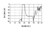
図25は、本実施の形態に係るバンドパスフィルタ100の挿入損失の周波数特性の一例を示している。図26は、第2の比較例のバンドパスフィルタの挿入損失の周波数特性の一例を示している。図25および図26に示した特性は、シミュレーションによって求めたものである。図25および図26において、横軸は周波数を示し、縦軸は挿入損失を示している。図25および図26に示した例では、バンドパスフィルタ100および第2の比較例のバンドパスフィルタの通過帯域は、約26〜30GHzであり、通過帯域の中心周波数は、約28GHzである。 FIG. 25 shows an example of the frequency characteristic of the insertion loss of the bandpass filter 100 according to the present embodiment. FIG. 26 shows an example of the frequency characteristic of the insertion loss of the bandpass filter of the second comparative example. The characteristics shown in FIGS. 25 and 26 are obtained by simulation. In FIGS. 25 and 26, the horizontal axis represents frequency and the vertical axis represents insertion loss. In the examples shown in FIGS. 25 and 26, the pass band of the bandpass filter 100 and the bandpass filter of the second comparative example is about 26 to 30 GHz, and the center frequency of the pass band is about 28 GHz.

シミュレーションにおけるバンドパスフィルタ100では、仕切り部107の存在を前提として、図25に示したように第1の通過帯域近傍領域と第2の通過帯域近傍領域の両方において挿入損失が急峻に変化する特性が得られるように、2つの飛び越し結合の大きさが調整されている。第1の通過帯域近傍領域は、約23〜26GHzの周波数領域である。第2の通過帯域近傍領域は、約30〜33GHzの周波数領域である。なお、図25に示した特性では、第2の通過帯域近傍領域において減衰極は明確には現れていない。これは、共振器152,155間の磁気結合によって第2の通過帯域近傍領域に生じる減衰極における挿入損失が、共振器151,156間の容量結合によって、幾分小さくなったためである。しかし、図25に示した特性では、第2の通過帯域近傍領域において、減衰極は明確には現れていないものの挿入損失が急峻に変化している。 In the bandpass filter 100 in the simulation, the insertion loss changes sharply in both the first passband vicinity region and the second passband vicinity region as shown in FIG. 25, assuming the presence of the partition portion 107. The size of the two jump couplings has been adjusted so that The region near the first pass band is a frequency region of about 23 to 26 GHz. The region near the second pass band is a frequency region of about 30 to 33 GHz. In the characteristics shown in FIG. 25, the attenuation pole does not clearly appear in the region near the second passband. This is because the insertion loss at the attenuation pole caused by the magnetic coupling between the resonators 152 and 155 in the region near the second passband is somewhat reduced by the capacitive coupling between the resonators 151 and 156. However, in the characteristics shown in FIG. 25, the insertion loss changes sharply in the region near the second pass band, although the attenuation pole does not clearly appear.

図26に示した第2の比較例のバンドパスフィルタの特性では、第1の通過帯域近傍領域と第2の通過帯域近傍領域の両方において、バンドパスフィルタ100に比べて、挿入損失が小さくなっている。これは、第2の比較例のバンドパスフィルタでは、仕切り部107を除いたことにより、共振器152,155間の磁気結合の大きさが、バンドパスフィルタ100において調整された大きさからずれたためである。 In the characteristics of the bandpass filter of the second comparative example shown in FIG. 26, the insertion loss is smaller than that of the bandpass filter 100 in both the region near the first passband and the region near the second passband. ing. This is because in the bandpass filter of the second comparative example, the size of the magnetic coupling between the resonators 152 and 155 deviates from the size adjusted in the bandpass filter 100 due to the removal of the partition portion 107. Is.

また、図26に示した比較例のバンドパスフィルタの特性では、50GHzに近い周波数領域において挿入損失が極端に小さくなるピークが存在している。これは、最低次導波管モードによる不要な共振が生じているためと考えられる。図25に示したバンドパスフィルタ100の特性では、50GHzに近い周波数領域に存在するピークが、図26に示した特性に比べて、より高い周波数側に移動し、且つこのピークにおける挿入損失が大きくなっている。そのため、図25に示した特性では、図26に示した特性に比べて、通過帯域よりも高い周波数領域における減衰特性は良好である。 Further, in the characteristics of the bandpass filter of the comparative example shown in FIG. 26, there is a peak in which the insertion loss becomes extremely small in the frequency region close to 50 GHz. It is considered that this is because unnecessary resonance occurs due to the lowest-order waveguide mode. In the characteristics of the bandpass filter 100 shown in FIG. 25, the peak existing in the frequency region close to 50 GHz moves to the higher frequency side as compared with the characteristics shown in FIG. 26, and the insertion loss at this peak is large. It has become. Therefore, in the characteristics shown in FIG. 25, the attenuation characteristics in the frequency region higher than the pass band are better than the characteristics shown in FIG. 26.

図25から、本実施の形態に係るバンドパスフィルタ100によれば、第1の通過帯域近傍領域と第2の通過帯域近傍領域の両方において挿入損失が急峻に変化し、且つ最低次導波管モードに起因した減衰特性の悪化が抑制された良好な特性を実現できることが分かる。 From FIG. 25, according to the bandpass filter 100 according to the present embodiment, the insertion loss changes sharply in both the region near the first passband and the region near the second passband, and the lowest-order waveguide It can be seen that good characteristics can be realized in which deterioration of damping characteristics due to the mode is suppressed.

本実施の形態におけるその他の構成、作用および効果は、第1の実施の形態と同様である。 Other configurations, actions and effects in this embodiment are similar to those in the first embodiment.

[第3の実施の形態]
次に、図27および図28を参照して、本発明の第3の実施の形態について説明する。図27は、本実施の形態に係るバンドパスフィルタの構造を示す斜視図である。図28は、本実施の形態に係るバンドパスフィルタの回路構成を示す回路図である。
[Third Embodiment]
Next, a third embodiment of the present invention will be described with reference to FIGS. 27 and 28. FIG. 27 is a perspective view showing the structure of the bandpass filter according to the present embodiment. FIG. 28 is a circuit diagram showing a circuit configuration of a bandpass filter according to the present embodiment.

本実施の形態に係るバンドパスフィルタ200は、本体2と、第1の入出力ポート3および第2の入出力ポート4と、3つ以上の共振器と、シールド6と、仕切り部207とを備えている。本体2は、積層体20を含んでいる。 The bandpass filter 200 according to the present embodiment has a main body 2, a first input / output port 3 and a second input / output port 4, three or more resonators, a shield 6, and a partition portion 207. I have. The main body 2 includes the laminated body 20.

3つ以上の共振器は、回路構成上、第1の入出力ポート3と第2の入出力ポート4の間に設けられている。本実施の形態では、3つ以上の共振器は、3つの共振器251,252,253である。3つの共振器251,252,253は、回路構成上、第1の入出力ポート3側からこの順に配置されている。3つの共振器251〜253は、回路構成上隣接する2つの共振器が電磁結合するように構成されている。すなわち、共振器251〜253は、共振器251,252が回路構成上隣接して電磁結合し、共振器252,253が回路構成上隣接して電磁結合するように構成されている。また、本実施の形態では特に、回路構成上隣接する2つの共振器の間の電磁結合は、容量結合である。また、本実施の形態では特に、共振器251〜253の各々は、両端開放型共振器であり且つ1/2波長共振器である。 Three or more resonators are provided between the first input / output port 3 and the second input / output port 4 in terms of circuit configuration. In this embodiment, the three or more resonators are three resonators 251,252,253. The three resonators 251, 252, and 253 are arranged in this order from the first input / output port 3 side in the circuit configuration. The three resonators 251 to 253 are configured such that two adjacent resonators are electromagnetically coupled in terms of circuit configuration. That is, the resonators 251 to 253 are configured such that the resonators 251,252 are electromagnetically coupled adjacent to each other in the circuit configuration and the resonators 252 and 253 are electromagnetically coupled adjacent to each other in the circuit configuration. Further, in the present embodiment, in particular, the electromagnetic coupling between two resonators adjacent to each other in the circuit configuration is a capacitive coupling. Further, in the present embodiment, in particular, each of the resonators 251 to 253 is an open-ended resonator and a 1/2 wavelength resonator.

シールド6の第1の部分61、第2の部分62および接続部63は、3つの共振器251〜253を囲むように配置されている。第1の部分61は、積層体20の主要部21の第1の端面21aに配置された第1の導体層610によって構成されている。第2の部分62は、積層体20の主要部21の第2の端面21bに配置された第2の導体層620によって構成されている。 The first portion 61, the second portion 62, and the connecting portion 63 of the shield 6 are arranged so as to surround the three resonators 251 to 253. The first portion 61 is composed of a first conductor layer 610 arranged on the first end surface 21a of the main portion 21 of the laminated body 20. The second portion 62 is composed of a second conductor layer 620 arranged on the second end surface 21b of the main portion 21 of the laminated body 20.

バンドパスフィルタ200は、共振器251,252間の容量結合を実現するキャパシタC212と、共振器252,253間の容量結合を実現するキャパシタC223とを備えている。 The bandpass filter 200 includes a capacitor C212 that realizes a capacitive coupling between the resonators 251,252 and a capacitor C223 that realizes a capacitive coupling between the resonators 252 and 253.

本実施の形態では、3つの共振器251〜253のうち回路構成上第1の入出力ポート3に最も近い共振器251と、3つの共振器251〜253のうち回路構成上第2の入出力ポート4に最も近い共振器253は、回路構成上隣接していないが磁気結合している。共振器251は、本発明における第1の共振器に対応する。共振器253は、本発明における第2の共振器に対応する。 In the present embodiment, the resonator 251 closest to the first input / output port 3 in the circuit configuration among the three resonators 251 to 253 and the second input / output in the circuit configuration among the three resonators 251 to 253. The resonator 253 closest to the port 4 is not adjacent in the circuit configuration but is magnetically coupled. The resonator 251 corresponds to the first resonator in the present invention. The resonator 253 corresponds to the second resonator in the present invention.

バンドパスフィルタ200は、更に、第1の入出力ポート3と共振器251との間に設けられたキャパシタC201と、第2の入出力ポート4と共振器253との間に設けられたキャパシタC202とを備えている。 The bandpass filter 200 further includes a capacitor C201 provided between the first input / output port 3 and the resonator 251 and a capacitor C202 provided between the second input / output port 4 and the resonator 253. And have.

バンドパスフィルタ200は、更に、第1の実施の形態と同様に、2つの線路91,92を備えている。 The bandpass filter 200 further includes two lines 91 and 92, as in the first embodiment.

共振器251は、導体よりなる共振器導体部2510を有している。共振器252は、導体よりなる共振器導体部2520を有している。共振器253は、導体よりなる共振器導体部2530を有している。共振器導体部2510は、本発明における第1の共振器導体部に対応する。共振器導体部2530は、本発明における第2の共振器導体部に対応する。 The resonator 251 has a resonator conductor portion 2510 made of a conductor. The resonator 252 has a resonator conductor portion 2520 made of a conductor. The resonator 253 has a resonator conductor portion 2530 made of a conductor. The resonator conductor portion 2510 corresponds to the first resonator conductor portion in the present invention. The resonator conductor portion 2530 corresponds to the second resonator conductor portion in the present invention.

共振器導体部2510,2520,2530は、第1の方向すなわちZ方向に関して、積層体20内の同じ位置に配置されている。また、共振器導体部2510,2520,2530の各々は、第1の方向すなわちZ方向と交差する方向に延びている。本実施の形態では特に、共振器導体部2510,2520,2530の各々は、第1の方向すなわちZ方向に直交する方向に延びている。 The resonator conductor portions 2510, 2520, 2530 are arranged at the same position in the laminated body 20 with respect to the first direction, that is, the Z direction. Further, each of the resonator conductor portions 2510, 2520, and 2530 extends in the first direction, that is, in the direction intersecting the Z direction. In this embodiment, in particular, each of the resonator conductor portions 2510, 2520, and 2530 extends in the first direction, that is, in the direction orthogonal to the Z direction.

共振器導体部2510,2520,2530の各々は、互いに反対側に位置する第1端と第2端を有している。前述のように、共振器251〜253の各々は、両端開放型共振器である。そのため、共振器導体部2510,2520,2530の各々の第1端と第2端は、いずれも開放されている。共振器導体部2510,2520,2530の各々は、バンドパスフィルタ200の通過帯域の中心周波数に対応する波長の1/2またはそれに近い長さを有している。 Each of the resonator conductor portions 2510, 2520, and 2530 has a first end and a second end located on opposite sides of each other. As described above, each of the resonators 251 to 253 is an open-ended resonator. Therefore, the first end and the second end of the resonator conductor portions 2510, 2520, and 2530 are all open. Each of the resonator conductors 2510, 2520, and 2530 has a length of 1/2 or close to the wavelength corresponding to the center frequency of the pass band of the bandpass filter 200.

仕切り部207は、その少なくとも一部が共振器導体部2510と共振器導体部2530の間を通過するように延びて、第1の部分61と第2の部分62とに接している。本実施の形態では特に、仕切り部207は、第1の方向すなわちZ方向に延びている。また、仕切り部207は、第1の部分61と第2の部分62を最短経路で接続している。すなわち、仕切り部207のZ方向の長さは、第1の部分61と第2の部分62の間の距離と等しい。 At least a part of the partition portion 207 extends so as to pass between the resonator conductor portion 2510 and the resonator conductor portion 2530, and is in contact with the first portion 61 and the second portion 62. In particular, in the present embodiment, the partition portion 207 extends in the first direction, that is, the Z direction. Further, the partition portion 207 connects the first portion 61 and the second portion 62 by the shortest path. That is, the length of the partition portion 207 in the Z direction is equal to the distance between the first portion 61 and the second portion 62.

また、仕切り部207は、主要部21を構成する2つ以上の誘電体層を貫通している。本実施の形態では、仕切り部207は、それぞれ主要部21を構成する2つ以上の誘電体層を貫通する複数のスルーホール列207Tを含んでいる。複数のスルーホール列207Tは、本発明における第1のスルーホール列に対応する。図27では、個々のスルーホール列207Tを円柱で表している。複数のスルーホール列207Tの各々は、直列に接続された2つ以上のスルーホールを含んでいる。複数のスルーホール列207Tの各々は、Z方向に延びている。 Further, the partition portion 207 penetrates two or more dielectric layers constituting the main portion 21. In the present embodiment, the partition portion 207 includes a plurality of through-hole rows 207T penetrating two or more dielectric layers each constituting the main portion 21. The plurality of through-hole rows 207T correspond to the first through-hole row in the present invention. In FIG. 27, each through-hole row 207T is represented by a cylinder. Each of the plurality of through-hole rows 207T includes two or more through-holes connected in series. Each of the plurality of through-hole rows 207T extends in the Z direction.

本実施の形態では、共振器導体部2510と共振器導体部2530は、Y方向に延び、所定の間隔を開けてX方向に隣接している。複数のスルーホール列207Tは、Y方向に並ぶように配列されて、共振器導体部2510と共振器導体部2530の間を通過するように配置されている。本実施の形態では、スルーホール列207Tの数は6である。 In the present embodiment, the resonator conductor portion 2510 and the resonator conductor portion 2530 extend in the Y direction and are adjacent to each other in the X direction with a predetermined interval. The plurality of through-hole rows 207T are arranged so as to be arranged in the Y direction and pass between the resonator conductor portion 2510 and the resonator conductor portion 2530. In this embodiment, the number of through-hole rows 207T is 6.

シールド6の接続部63は、それぞれ主要部21を構成する2つ以上の誘電体層を貫通する複数のスルーホール列263Tを含んでいる。複数のスルーホール列263Tは、本発明における第2のスルーホール列に対応する。図27では、個々のスルーホール列263Tを円柱で表している。図27において、6つのスルーホール列207T以外の複数の円柱で表わされた複数のスルーホール列は、全てスルーホール列263Tである。複数のスルーホール列263Tの各々は、直列に接続された2つ以上のスルーホールを含んでいる。複数のスルーホール列263Tの各々は、Z方向に延びている。 The connection portion 63 of the shield 6 includes a plurality of through-hole rows 263T penetrating two or more dielectric layers each constituting the main portion 21. The plurality of through-hole rows 263T correspond to the second through-hole row in the present invention. In FIG. 27, each through-hole row 263T is represented by a cylinder. In FIG. 27, the plurality of through-hole rows represented by the plurality of cylinders other than the six through-hole rows 207T are all through-hole rows 263T. Each of the plurality of through-hole rows 263T includes two or more through-holes connected in series. Each of the plurality of through-hole rows 263T extends in the Z direction.

バンドパスフィルタ200は、更に、積層体20内に設けられた導体層211,212,221,222を備えている。 The bandpass filter 200 further includes conductor layers 211,212,221,222 provided in the laminate 20.

導体層211は、互いに反対側に位置する第1端と第2端を有している。導体層211における第1端の近傍部分は、積層体20内に設けられた複数のスルーホールを介して第1の入出力ポート3に接続されている。導体層211における第2端の近傍部分は、1つ以上の誘電体層を介して、共振器導体部2510における第1端の近傍部分に対向している。これにより、キャパシタC201が構成されている。線路91は、導体層211と第1の入出力ポート3を接続する複数のスルーホールのうちの1つ以上のスルーホールを介して、第1の入出力ポート3に接続されている。 The conductor layer 211 has a first end and a second end located on opposite sides of each other. A portion of the conductor layer 211 near the first end is connected to the first input / output port 3 via a plurality of through holes provided in the laminated body 20. The portion near the second end of the conductor layer 211 faces the portion near the first end of the resonator conductor portion 2510 via one or more dielectric layers. As a result, the capacitor C201 is configured. The line 91 is connected to the first input / output port 3 via one or more through holes among the plurality of through holes connecting the conductor layer 211 and the first input / output port 3.

導体層212は、互いに反対側に位置する第1端と第2端を有している。導体層212における第1端の近傍部分は、積層体20内に設けられた複数のスルーホールを介して第2の入出力ポート4に接続されている。導体層212における第2端の近傍部分は、1つ以上の誘電体層を介して、共振器導体部2530における第1端の近傍部分に対向している。これにより、キャパシタC202が構成されている。線路92は、導体層212と第2の入出力ポート4を接続する複数のスルーホールのうちの1つ以上のスルーホールを介して、第2の入出力ポート4に接続されている。 The conductor layer 212 has a first end and a second end located on opposite sides of each other. A portion of the conductor layer 212 in the vicinity of the first end is connected to the second input / output port 4 via a plurality of through holes provided in the laminated body 20. The portion near the second end of the conductor layer 212 faces the vicinity of the first end of the resonator conductor portion 2530 via one or more dielectric layers. As a result, the capacitor C202 is configured. The line 92 is connected to the second input / output port 4 via one or more through holes among the plurality of through holes connecting the conductor layer 212 and the second input / output port 4.

導体層221は、1つ以上の誘電体層を介して、共振器導体部2510における第2端の近傍部分と共振器導体部2520における第1端の近傍部分とに対向している。これにより、キャパシタC212が構成されている。 The conductor layer 221 faces a portion near the second end of the resonator conductor portion 2510 and a portion near the first end of the resonator conductor portion 2520 via one or more dielectric layers. As a result, the capacitor C212 is configured.

導体層222は、1つ以上の誘電体層を介して、共振器導体部2520における第2端の近傍部分と共振器導体部2530における第2端の近傍部分とに対向している。これにより、キャパシタC223が構成されている。 The conductor layer 222 faces a portion near the second end of the resonator conductor portion 2520 and a portion near the second end of the resonator conductor portion 2530 via one or more dielectric layers. As a result, the capacitor C223 is configured.

本実施の形態では、仕切り部207によって、シールド6で囲まれた空間が、共振器導体部2510が存在する空間と、共振器導体部2530が存在する空間とに仕切られる。これにより、本実施の形態によれば、第1の実施の形態と同様に、最低次導波管モードによって通過帯域よりも高い周波数領域における減衰特性が悪化することを防止することができる。 In the present embodiment, the space surrounded by the shield 6 is partitioned by the partition portion 207 into a space in which the resonator conductor portion 2510 exists and a space in which the resonator conductor portion 2530 exists. Thereby, according to the present embodiment, as in the first embodiment, it is possible to prevent the attenuation characteristic from being deteriorated in the frequency region higher than the pass band due to the lowest-order waveguide mode.

また、本実施の形態では、回路構成上隣接していない1段目の共振器251と3段目の共振器253が磁気結合している。共振器251,253間の磁気結合は、挿入損失の周波数特性において、通過帯域よりも低く通過帯域に近い周波数領域である第1の通過帯域近傍領域に、減衰極を生じさせることができる。 Further, in the present embodiment, the first-stage resonator 251 and the third-stage resonator 253, which are not adjacent to each other in the circuit configuration, are magnetically coupled. The magnetic coupling between the resonators 251, 253 can generate an attenuation pole in a region near the first pass band, which is a frequency region lower than the pass band and close to the pass band in the frequency characteristic of the insertion loss.

これらのことから、本実施の形態に係るバンドパスフィルタ200によれば、第1の通過帯域近傍領域において挿入損失が急峻に変化し、且つ最低次導波管モードに起因した減衰特性の悪化が抑制された良好な特性を実現することができる。 From these facts, according to the bandpass filter 200 according to the present embodiment, the insertion loss changes sharply in the region near the first pass band, and the attenuation characteristic deteriorates due to the lowest-order waveguide mode. Suppressed good characteristics can be achieved.

本実施の形態におけるその他の構成、作用および効果は、第1の実施の形態と同様である。 Other configurations, actions and effects in this embodiment are similar to those in the first embodiment.

[第4の実施の形態]
次に、図29および図30を参照して、本発明の第4の実施の形態について説明する。図29は、本実施の形態に係るバンドパスフィルタの構造を示す斜視図である。図30は、本実施の形態に係るバンドパスフィルタの回路構成を示す回路図である。
[Fourth Embodiment]
Next, a fourth embodiment of the present invention will be described with reference to FIGS. 29 and 30. FIG. 29 is a perspective view showing the structure of the bandpass filter according to the present embodiment. FIG. 30 is a circuit diagram showing a circuit configuration of a bandpass filter according to the present embodiment.

本実施の形態に係るバンドパスフィルタ300は、本体2と、第1の入出力ポート3および第2の入出力ポート4と、3つ以上の共振器と、シールド6と、仕切り部307とを備えている。本体2は、積層体20を含んでいる。 The bandpass filter 300 according to the present embodiment includes a main body 2, a first input / output port 3 and a second input / output port 4, three or more resonators, a shield 6, and a partition portion 307. I have. The main body 2 includes the laminated body 20.

3つ以上の共振器は、回路構成上、第1の入出力ポート3と第2の入出力ポート4の間に設けられている。本実施の形態では、3つ以上の共振器は、4つの共振器351,352,353,354である。4つの共振器351,352,353,354は、回路構成上、第1の入出力ポート3側からこの順に配置されている。4つの共振器351〜354は、回路構成上隣接する2つの共振器が電磁結合するように構成されている。すなわち、共振器351〜354は、共振器351,352が回路構成上隣接して電磁結合し、共振器352,353が回路構成上隣接して電磁結合し、共振器353,354が回路構成上隣接して電磁結合するように構成されている。また、本実施の形態では特に、回路構成上隣接する2つの共振器の間の電磁結合は、容量結合である。また、本実施の形態では特に、共振器351〜354の各々は、両端開放型共振器であり且つ1/2波長共振器である。 Three or more resonators are provided between the first input / output port 3 and the second input / output port 4 in terms of circuit configuration. In this embodiment, the three or more resonators are four resonators 351,352,353,354. The four resonators 351, 352, 353, 354 are arranged in this order from the first input / output port 3 side in the circuit configuration. The four resonators 351 to 354 are configured such that two resonators adjacent to each other in the circuit configuration are electromagnetically coupled. That is, in the resonators 351 to 354, the resonators 351 and 352 are electromagnetically coupled adjacent to each other in the circuit configuration, the resonators 352 and 353 are electromagnetically coupled adjacent to each other in the circuit configuration, and the resonators 353 and 354 are electromagnetically coupled in the circuit configuration. It is configured to be electromagnetically coupled adjacent to each other. Further, in the present embodiment, in particular, the electromagnetic coupling between two resonators adjacent to each other in the circuit configuration is a capacitive coupling. Further, in the present embodiment, in particular, each of the resonators 351 to 354 is an open-ended resonator and a 1/2 wavelength resonator.

シールド6の第1の部分61、第2の部分62および接続部63は、4つの共振器351〜354を囲むように配置されている。第1の部分61は、積層体20の主要部21の第1の端面21aに配置された第1の導体層610によって構成されている。第2の部分62は、積層体20の主要部21の第2の端面21bに配置された第2の導体層620によって構成されている。 The first portion 61, the second portion 62, and the connecting portion 63 of the shield 6 are arranged so as to surround the four resonators 351 to 354. The first portion 61 is composed of a first conductor layer 610 arranged on the first end surface 21a of the main portion 21 of the laminated body 20. The second portion 62 is composed of a second conductor layer 620 arranged on the second end surface 21b of the main portion 21 of the laminated body 20.

バンドパスフィルタ300は、共振器351,352間の容量結合を実現するキャパシタC312と、共振器352,353間の容量結合を実現するキャパシタC323と、共振器353,354間の容量結合を実現するキャパシタC334とを備えている。 The bandpass filter 300 realizes the capacitive coupling between the resonators C312 which realizes the capacitive coupling between the resonators 351 and 352, the capacitor C323 which realizes the capacitive coupling between the resonators 352 and 353, and the resonators 353 and 354. It includes a capacitor C334.

本実施の形態では、4つの共振器351〜354のうち回路構成上第1の入出力ポート3に最も近い共振器351と、4つの共振器351〜354のうち回路構成上第2の入出力ポート4に最も近い共振器354は、回路構成上隣接していないが磁気結合している。共振器351は、本発明における第1の共振器に対応する。共振器354は、本発明における第2の共振器に対応する。 In the present embodiment, the resonator 351 closest to the first input / output port 3 in the circuit configuration among the four resonators 351 to 354 and the second input / output in the circuit configuration among the four resonators 351 to 354 The resonator 354 closest to the port 4 is not adjacent in the circuit configuration but is magnetically coupled. The resonator 351 corresponds to the first resonator in the present invention. The resonator 354 corresponds to the second resonator in the present invention.

バンドパスフィルタ300は、更に、第1の入出力ポート3と共振器351との間に設けられたキャパシタC301と、第2の入出力ポート4と共振器354との間に設けられたキャパシタC302とを備えている。 The bandpass filter 300 further includes a capacitor C301 provided between the first input / output port 3 and the resonator 351 and a capacitor C302 provided between the second input / output port 4 and the resonator 354. And have.

バンドパスフィルタ300は、更に、第1の実施の形態と同様に、2つの線路91,92を備えている。 The bandpass filter 300 further includes two lines 91 and 92, as in the first embodiment.

共振器351は、導体よりなる共振器導体部3510を有している。共振器352は、導体よりなる共振器導体部3520を有している。共振器353は、導体よりなる共振器導体部3530を有している。共振器354は、導体よりなる共振器導体部3540を有している。共振器導体部3510は、本発明における第1の共振器導体部に対応する。共振器導体部3540は、本発明における第2の共振器導体部に対応する。 The resonator 351 has a resonator conductor portion 3510 made of a conductor. The resonator 352 has a resonator conductor portion 3520 made of a conductor. The resonator 353 has a resonator conductor portion 3530 made of a conductor. The resonator 354 has a resonator conductor portion 3540 made of a conductor. The resonator conductor portion 3510 corresponds to the first resonator conductor portion in the present invention. The resonator conductor portion 3540 corresponds to the second resonator conductor portion in the present invention.

共振器導体部3510,3520,3530,3540は、第1の方向すなわちZ方向に関して、積層体20内の同じ位置に配置されている。また、共振器導体部3510,3520,3530,3540の各々は、第1の方向すなわちZ方向と交差する方向に延びている。本実施の形態では特に、共振器導体部3510,3520,3530,3540の各々は、第1の方向すなわちZ方向に直交する方向に延びている。 The resonator conductor portions 3510, 3520, 3530, and 3540 are arranged at the same position in the laminated body 20 with respect to the first direction, that is, the Z direction. Further, each of the resonator conductor portions 3510, 3520, 3530, and 3540 extends in the first direction, that is, in the direction intersecting the Z direction. In this embodiment, in particular, each of the resonator conductor portions 3510, 3520, 3530, and 3540 extends in the first direction, that is, in the direction orthogonal to the Z direction.

共振器導体部3510,3520,3530,3540の各々は、互いに反対側に位置する第1端と第2端を有している。前述のように、共振器351〜354の各々は、両端開放型共振器である。そのため、共振器導体部3510,3520,3530,3540の各々の第1端と第2端は、いずれも開放されている。共振器導体部3510,3520,3530,3540の各々は、バンドパスフィルタ300の通過帯域の中心周波数に対応する波長の1/2またはそれに近い長さを有している。 Each of the resonator conductor portions 3510, 3520, 3530, and 3540 has a first end and a second end located on opposite sides of each other. As described above, each of the resonators 351 to 354 is an open-ended resonator. Therefore, the first end and the second end of each of the resonator conductor portions 3510, 3520, 3530, and 3540 are open. Each of the resonator conductor portions 3510, 3520, 3530, and 3540 has a length of 1/2 or close to the wavelength corresponding to the center frequency of the pass band of the bandpass filter 300.

仕切り部307は、その少なくとも一部が共振器導体部3510と共振器導体部3540の間を通過するように延びて、第1の部分61と第2の部分62とに接している。本実施の形態では特に、仕切り部307は、第1の方向すなわちZ方向に延びている。また、仕切り部307は、第1の部分61と第2の部分62を最短経路で接続している。すなわち、仕切り部307のZ方向の長さは、第1の部分61と第2の部分62の間の距離と等しい。 At least a part of the partition portion 307 extends so as to pass between the resonator conductor portion 3510 and the resonator conductor portion 3540, and is in contact with the first portion 61 and the second portion 62. In particular, in the present embodiment, the partition portion 307 extends in the first direction, that is, the Z direction. Further, the partition portion 307 connects the first portion 61 and the second portion 62 by the shortest path. That is, the length of the partition portion 307 in the Z direction is equal to the distance between the first portion 61 and the second portion 62.

また、仕切り部307は、主要部21を構成する2つ以上の誘電体層を貫通している。本実施の形態では、仕切り部307は、それぞれ主要部21を構成する2つ以上の誘電体層を貫通する複数のスルーホール列307Tを含んでいる。複数のスルーホール列307Tは、本発明における第1のスルーホール列に対応する。図29では、個々のスルーホール列307Tを円柱で表している。複数のスルーホール列307Tの各々は、直列に接続された2つ以上のスルーホールを含んでいる。複数のスルーホール列307Tの各々は、Z方向に延びている。 Further, the partition portion 307 penetrates two or more dielectric layers constituting the main portion 21. In the present embodiment, the partition portion 307 includes a plurality of through-hole rows 307T penetrating two or more dielectric layers each constituting the main portion 21. The plurality of through-hole rows 307T correspond to the first through-hole row in the present invention. In FIG. 29, each through-hole row 307T is represented by a cylinder. Each of the plurality of through-hole rows 307T includes two or more through-holes connected in series. Each of the plurality of through-hole rows 307T extends in the Z direction.

本実施の形態では、共振器導体部3510と共振器導体部3540は、Y方向に延び、所定の間隔を開けてX方向に隣接している。複数のスルーホール列307Tは、Y方向に並ぶように配列されて、共振器導体部3510と共振器導体部3540の間を通過するように配置されている。本実施の形態では、スルーホール列307Tの数は6である。 In the present embodiment, the resonator conductor portion 3510 and the resonator conductor portion 3540 extend in the Y direction and are adjacent to each other in the X direction with a predetermined interval. The plurality of through-hole rows 307T are arranged so as to be arranged in the Y direction and pass between the resonator conductor portion 3510 and the resonator conductor portion 3540. In this embodiment, the number of through-hole rows 307T is 6.

シールド6の接続部63は、それぞれ主要部21を構成する2つ以上の誘電体層を貫通する複数のスルーホール列363Tを含んでいる。複数のスルーホール列363Tは、本発明における第2のスルーホール列に対応する。図29では、個々のスルーホール列363Tを円柱で表している。図29において、6つのスルーホール列307T以外の複数の円柱で表わされた複数のスルーホール列は、全てスルーホール列363Tである。複数のスルーホール列363Tの各々は、直列に接続された2つ以上のスルーホールを含んでいる。複数のスルーホール列363Tの各々は、Z方向に延びている。 The connection portion 63 of the shield 6 includes a plurality of through-hole rows 363T penetrating two or more dielectric layers each constituting the main portion 21. The plurality of through-hole rows 363T correspond to the second through-hole row in the present invention. In FIG. 29, each through-hole row 363T is represented by a cylinder. In FIG. 29, the plurality of through-hole rows represented by the plurality of cylinders other than the six through-hole rows 307T are all through-hole rows 363T. Each of the plurality of through-hole rows 363T includes two or more through-holes connected in series. Each of the plurality of through-hole rows 363T extends in the Z direction.

バンドパスフィルタ300は、更に、積層体20内に設けられた導体層311,312,321,322,323を備えている。 The bandpass filter 300 further includes a conductor layer 311, 312, 3211, 322, 323 provided in the laminated body 20.

導体層311は、互いに反対側に位置する第1端と第2端を有している。導体層311における第1端の近傍部分は、積層体20内に設けられた複数のスルーホールを介して第1の入出力ポート3に接続されている。導体層311における第2端の近傍部分は、1つ以上の誘電体層を介して、共振器導体部3510における第1端の近傍部分に対向している。これにより、キャパシタC301が構成されている。線路91は、導体層311と第1の入出力ポート3を接続する複数のスルーホールのうちの1つ以上のスルーホールを介して、第1の入出力ポート3に接続されている。 The conductor layer 311 has a first end and a second end located on opposite sides of each other. A portion of the conductor layer 311 near the first end is connected to the first input / output port 3 via a plurality of through holes provided in the laminated body 20. The portion near the second end of the conductor layer 311 faces the vicinity of the first end of the resonator conductor portion 3510 via one or more dielectric layers. As a result, the capacitor C301 is configured. The line 91 is connected to the first input / output port 3 via one or more through holes among the plurality of through holes connecting the conductor layer 311 and the first input / output port 3.

導体層312は、互いに反対側に位置する第1端と第2端を有している。導体層312における第1端の近傍部分は、積層体20内に設けられた複数のスルーホールを介して第2の入出力ポート4に接続されている。導体層312における第2端の近傍部分は、1つ以上の誘電体層を介して、共振器導体部3540における第1端の近傍部分に対向している。これにより、キャパシタC302が構成されている。線路92は、導体層312と第2の入出力ポート4を接続する複数のスルーホールのうちの1つ以上のスルーホールを介して、第2の入出力ポート4に接続されている。 The conductor layer 312 has a first end and a second end located on opposite sides of each other. A portion of the conductor layer 312 near the first end is connected to the second input / output port 4 via a plurality of through holes provided in the laminated body 20. The portion near the second end of the conductor layer 312 faces the portion near the first end of the resonator conductor portion 3540 via one or more dielectric layers. As a result, the capacitor C302 is configured. The line 92 is connected to the second input / output port 4 via one or more through holes among the plurality of through holes connecting the conductor layer 312 and the second input / output port 4.

導体層321は、1つ以上の誘電体層を介して、共振器導体部3510における第2端の近傍部分と共振器導体部3520における第1端の近傍部分とに対向している。これにより、キャパシタC312が構成されている。 The conductor layer 321 faces a portion near the second end of the resonator conductor portion 3510 and a portion near the first end of the resonator conductor portion 3520 via one or more dielectric layers. As a result, the capacitor C312 is configured.

導体層322は、1つ以上の誘電体層を介して、共振器導体部3520における第1端の近傍部分と共振器導体部3530における第1端の近傍部分とに対向している。これにより、キャパシタC323が構成されている。 The conductor layer 322 faces a portion near the first end of the resonator conductor portion 3520 and a portion near the first end of the resonator conductor portion 3530 via one or more dielectric layers. As a result, the capacitor C323 is configured.

導体層323は、1つ以上の誘電体層を介して、共振器導体部3530における第1端の近傍部分と共振器導体部3540における第2端の近傍部分とに対向している。これにより、キャパシタC334が構成されている。 The conductor layer 323 faces a portion near the first end of the resonator conductor portion 3530 and a portion near the second end of the resonator conductor portion 3540 via one or more dielectric layers. As a result, the capacitor C334 is configured.

本実施の形態では、仕切り部307によって、シールド6で囲まれた空間が、共振器導体部3510が存在する空間と、共振器導体部3540が存在する空間とに仕切られる。これにより、本実施の形態によれば、第1の実施の形態と同様に、最低次導波管モードによって通過帯域よりも高い周波数領域における減衰特性が悪化することを防止することができる。 In the present embodiment, the space surrounded by the shield 6 is partitioned by the partition portion 307 into a space in which the resonator conductor portion 3510 exists and a space in which the resonator conductor portion 3540 exists. Thereby, according to the present embodiment, as in the first embodiment, it is possible to prevent the attenuation characteristic from being deteriorated in the frequency region higher than the pass band due to the lowest-order waveguide mode.

また、本実施の形態では、回路構成上隣接していない1段目の共振器351と4段目の共振器354が磁気結合している。共振器351,354間の磁気結合は、挿入損失の周波数特性において、通過帯域よりも低く通過帯域に近い周波数領域である第1の通過帯域近傍領域と、通過帯域よりも高く通過帯域に近い周波数領域である第2の通過帯域近傍領域の両方に、減衰極を生じさせることができる。 Further, in the present embodiment, the first-stage resonator 351 and the fourth-stage resonator 354, which are not adjacent to each other in the circuit configuration, are magnetically coupled. In the frequency characteristics of the insertion loss, the magnetic coupling between the resonators 351 and 354 has a frequency near the first pass band, which is a frequency region lower than the pass band and close to the pass band, and a frequency higher than the pass band and close to the pass band. Damping poles can be generated in both the regions near the second passband, which is the region.

これらのことから、本実施の形態に係るバンドパスフィルタ300によれば、第1の通過帯域近傍領域と第2の通過帯域近傍領域の両方において挿入損失が急峻に変化し、且つ最低次導波管モードに起因した減衰特性の悪化が抑制された良好な特性を実現することができる。 From these facts, according to the bandpass filter 300 according to the present embodiment, the insertion loss changes sharply in both the region near the first passband and the region near the second passband, and the lowest-order waveguide is performed. It is possible to realize good characteristics in which deterioration of damping characteristics due to the tube mode is suppressed.

本実施の形態におけるその他の構成、作用および効果は、第1の実施の形態と同様である。 Other configurations, actions and effects in this embodiment are similar to those in the first embodiment.

なお、本発明は、上記各実施の形態に限定されず、種々の変更が可能である。例えば、共振器の数や構成は、各実施の形態に示したものに限らず、特許請求の範囲を満たすものであればよい。また、シールド6の接続部の少なくとも一部は、複数のスルーホール列の代わりに、本体2の1つ以上の側面に形成した導体層によって構成してもよい。また、仕切り部は、複数のスルーホール列の代わりに、板状の導体部によって構成してもよい。 The present invention is not limited to each of the above embodiments, and various modifications can be made. For example, the number and configuration of the resonators are not limited to those shown in each embodiment, and may satisfy the scope of claims. Further, at least a part of the connecting portion of the shield 6 may be formed by a conductor layer formed on one or more side surfaces of the main body 2 instead of a plurality of through-hole rows. Further, the partition portion may be formed by a plate-shaped conductor portion instead of a plurality of through-hole rows.

1…バンドパスフィルタ、2…本体、3…第1の入出力ポート、4…第2の入出力ポート、6…シールド、7…第1の仕切り部、7T…スルーホール列、20…積層体、21…主要部、22…被覆部、31〜48…誘電体層、51,52,53,54,55…共振器、61…第1の部分、62…第2の部分、63…接続部、63T…スルーホール列。 1 ... Bandpass filter, 2 ... Main body, 3 ... 1st input / output port, 4 ... 2nd input / output port, 6 ... Shield, 7 ... 1st partition, 7T ... Through hole row, 20 ... Laminate , 21 ... Main part, 22 ... Coating part, 31-48 ... Dielectric layer, 51, 52, 53, 54, 55 ... Resonator, 61 ... First part, 62 ... Second part, 63 ... Connection part , 63T ... Through hole row.

Claims (14)

誘電体よりなる本体と、
前記本体に一体化された第1の入出力ポートおよび第2の入出力ポートと、
前記本体内に設けられていると共に、回路構成上前記第1の入出力ポートと前記第2の入出力ポートの間に設けられ、回路構成上隣接する2つの共振器が電磁結合するように構成された3つ以上の共振器と、
導体よりなり、前記本体に一体化されたシールドと、
導体よりなり、前記本体内に設けられて、前記シールドに電気的に接続された仕切り部とを備えたバンドパスフィルタであって、
前記シールドは、第1の方向について間隔を開けて配置された第1の部分および第2の部分と、前記第1の部分と前記第2の部分を接続する接続部とを含み、
前記第1の部分、前記第2の部分および前記接続部は、前記3つ以上の共振器を囲むように配置され、
前記3つ以上の共振器は、回路構成上隣接していないが磁気結合する第1の共振器と第2の共振器を含み、
前記第1の共振器は、導体よりなる第1の共振器導体部を有し、
前記第2の共振器は、導体よりなる第2の共振器導体部を有し、
前記第1の共振器導体部と前記第2の共振器導体部の各々は、前記第1の方向と交差する方向に延び、
前記仕切り部は、その少なくとも一部が前記第1の共振器導体部のうち前記磁気結合を実現する部分と前記第2の共振器導体部のうち前記磁気結合を実現する部分の間を通過するように延びて、前記第1の部分と前記第2の部分とに接していることを特徴とするバンドパスフィルタ。
The body made of dielectric and
A first input / output port and a second input / output port integrated with the main body,
It is provided in the main body and is provided between the first input / output port and the second input / output port in the circuit configuration so that two resonators adjacent to each other in the circuit configuration are electromagnetically coupled. With 3 or more resonators
A shield made of a conductor and integrated with the main body,
A bandpass filter made of a conductor, provided in the main body, and provided with a partition portion electrically connected to the shield.
The shield includes a first portion and a second portion spaced apart from each other in the first direction, and a connecting portion connecting the first portion and the second portion.
The first portion, the second portion, and the connection portion are arranged so as to surround the three or more resonators.
The three or more resonators include a first resonator and a second resonator that are not adjacent to each other in the circuit configuration but are magnetically coupled.
The first resonator has a first resonator conductor portion made of a conductor.
The second resonator has a second resonator conductor portion made of a conductor.
Each of the first resonator conductor portion and the second resonator conductor portion extends in a direction intersecting the first direction.
At least a part of the partition passes between the portion of the first resonator conductor portion that realizes the magnetic coupling and the portion of the second resonator conductor portion that realizes the magnetic coupling. A bandpass filter that extends in such a manner and is in contact with the first portion and the second portion.
前記回路構成上隣接する2つの共振器の間の電磁結合は、容量結合であることを特徴とする請求項1記載のバンドパスフィルタ。 The bandpass filter according to claim 1, wherein the electromagnetic coupling between two resonators adjacent to each other in the circuit configuration is a capacitive coupling. 前記3つ以上の共振器の各々は、両端開放型共振器であることを特徴とする請求項1または2記載のバンドパスフィルタ。 The bandpass filter according to claim 1 or 2, wherein each of the three or more resonators is an open-ended resonator. 前記仕切り部は、前記第1の方向に延びて、前記第1の部分と前記第2の部分を最短経路で接続することを特徴とする請求項1ないし3のいずれかに記載のバンドパスフィルタ。 The bandpass filter according to any one of claims 1 to 3, wherein the partition portion extends in the first direction and connects the first portion and the second portion by the shortest path. .. 前記第1の共振器は、回路構成上前記第1の入出力ポートに最も近い共振器であり、
前記第2の共振器は、回路構成上前記第2の入出力ポートに最も近い共振器であることを特徴とする請求項1ないし4のいずれかに記載のバンドパスフィルタ。
The first resonator is the resonator closest to the first input / output port in terms of circuit configuration.
The bandpass filter according to any one of claims 1 to 4, wherein the second resonator is a resonator closest to the second input / output port in terms of circuit configuration.
前記3つ以上の共振器は、5つの共振器であることを特徴とする請求項5記載のバンドパスフィルタ。 The bandpass filter according to claim 5, wherein the three or more resonators are five resonators. 前記第1の共振器は、回路構成上前記第1の入出力ポートに対して2番目に近い共振器であり、
前記第2の共振器は、回路構成上前記第2の入出力ポートに対して2番目に近い共振器であることを特徴とする請求項1ないし4のいずれかに記載のバンドパスフィルタ。
The first resonator is a resonator that is second closest to the first input / output port in terms of circuit configuration.
The bandpass filter according to any one of claims 1 to 4, wherein the second resonator is a resonator that is second closest to the second input / output port in terms of circuit configuration.
前記3つ以上の共振器は、6つの共振器であることを特徴とする請求項7記載のバンドパスフィルタ。 The bandpass filter according to claim 7, wherein the three or more resonators are six resonators. 更に、通過帯域よりも高い所定の周波数の信号を減衰させるためのノッチフィルタ部を備えたことを特徴とする請求項1ないし8のいずれかに記載のバンドパスフィルタ。 The bandpass filter according to any one of claims 1 to 8, further comprising a notch filter unit for attenuating a signal having a predetermined frequency higher than the pass band. 前記本体は、前記第1の方向に積層された複数の誘電体層からなる積層体を含むことを特徴とする請求項1ないし9のいずれかに記載のバンドパスフィルタ。 The bandpass filter according to any one of claims 1 to 9, wherein the main body includes a laminated body composed of a plurality of dielectric layers laminated in the first direction. 前記積層体は、前記複数の誘電体層のうちの、積層された2つ以上の誘電体層からなる主要部を含み、
前記主要部は、2つ以上の誘電体層の前記第1の方向における両端に位置する第1の端面と第2の端面を有し、
前記第1の部分は、前記第1の端面に配置された第1の導体層によって構成され、
前記第2の部分は、前記第2の端面に配置された第2の導体層によって構成され、
前記仕切り部は、前記2つ以上の誘電体層を貫通していることを特徴とする請求項10記載のバンドパスフィルタ。
The laminated body includes a main portion composed of two or more laminated dielectric layers among the plurality of dielectric layers.
The main portion has a first end face and a second end face located at both ends of the two or more dielectric layers in the first direction.
The first portion is composed of a first conductor layer arranged on the first end face.
The second portion is composed of a second conductor layer arranged on the second end face.
The bandpass filter according to claim 10, wherein the partition portion penetrates the two or more dielectric layers.
前記仕切り部は、それぞれ前記2つ以上の誘電体層を貫通する複数の第1のスルーホール列を含み、
前記複数の第1のスルーホール列の各々は、直列に接続された2つ以上のスルーホールを含むことを特徴とする請求項11記載のバンドパスフィルタ。
The dividers each include a plurality of first through-hole rows penetrating the two or more dielectric layers.
11. The bandpass filter according to claim 11, wherein each of the plurality of first through-hole rows includes two or more through-holes connected in series.
前記シールドの前記接続部は、それぞれ前記2つ以上の誘電体層を貫通する複数の第2のスルーホール列を含み、
前記複数の第2のスルーホール列の各々は、直列に接続された2つ以上のスルーホールを含むことを特徴とする請求項11または12記載のバンドパスフィルタ。
The connection of the shield includes a plurality of second through-hole rows, each penetrating the two or more dielectric layers.
The bandpass filter according to claim 11 or 12, wherein each of the plurality of second through-hole rows includes two or more through-holes connected in series.
前記第1の共振器導体部と前記第2の共振器導体部は、前記第1の方向に関して、前記積層体内の同じ位置に配置されていることを特徴とする請求項10ないし13のいずれかに記載のバンドパスフィルタ。 Any of claims 10 to 13, wherein the first resonator conductor portion and the second resonator conductor portion are arranged at the same position in the laminate with respect to the first direction. Bandpass filter described in.
JP2017249867A 2017-12-26 2017-12-26 Bandpass filter Active JP6965732B2 (en)

Priority Applications (3)

Application Number Priority Date Filing Date Title
JP2017249867A JP6965732B2 (en) 2017-12-26 2017-12-26 Bandpass filter
US16/179,059 US10784551B2 (en) 2017-12-26 2018-11-02 Band-pass filter
CN201811599319.5A CN110011006B (en) 2017-12-26 2018-12-26 Band-pass filter

Applications Claiming Priority (1)

Application Number Priority Date Filing Date Title
JP2017249867A JP6965732B2 (en) 2017-12-26 2017-12-26 Bandpass filter

Publications (2)

Publication Number Publication Date
JP2019117970A JP2019117970A (en) 2019-07-18
JP6965732B2 true JP6965732B2 (en) 2021-11-10

Family

ID=66951486

Family Applications (1)

Application Number Title Priority Date Filing Date
JP2017249867A Active JP6965732B2 (en) 2017-12-26 2017-12-26 Bandpass filter

Country Status (3)

Country Link
US (1) US10784551B2 (en)
JP (1) JP6965732B2 (en)
CN (1) CN110011006B (en)

Families Citing this family (6)

* Cited by examiner, † Cited by third party
Publication number Priority date Publication date Assignee Title
JP7155499B2 (en) * 2017-04-26 2022-10-19 Tdk株式会社 LAMINATED ELECTRONIC COMPONENT AND MANUFACTURING METHOD THEREOF
US10871807B2 (en) * 2017-07-24 2020-12-22 Green Revolution Cooling, Inc. Power distribution system with thermal cutoff for dielectric cooling systems
CN114747087A (en) * 2019-12-09 2022-07-12 株式会社村田制作所 Dielectric waveguide resonator and dielectric waveguide filter
WO2021117354A1 (en) * 2019-12-09 2021-06-17 株式会社村田製作所 Dielectric waveguide filter
CN114788087A (en) * 2021-09-23 2022-07-22 香港应用科技研究院有限公司 Multilayer band-pass filter
US11575189B1 (en) * 2021-09-23 2023-02-07 Hong Kong Applied Science And Technology Research Institute Co., Ltd Multi-layer bandpass filter

Family Cites Families (21)

* Cited by examiner, † Cited by third party
Publication number Priority date Publication date Assignee Title
JPS6277703A (en) * 1985-09-30 1987-04-09 Murata Mfg Co Ltd Dielectric filter
JPS63267001A (en) * 1987-04-24 1988-11-04 Matsushita Electric Ind Co Ltd Polar filter
JPH07249902A (en) * 1994-03-09 1995-09-26 Mitsubishi Electric Corp Strip line filter and connection means between strip line filter and microstrip line
JPH08181506A (en) * 1994-12-22 1996-07-12 Sumitomo Special Metals Co Ltd Dielectric filter
JP3379326B2 (en) * 1996-02-20 2003-02-24 三菱電機株式会社 High frequency filter
JPH10190309A (en) * 1996-12-27 1998-07-21 Kyocera Corp Lamination type dielectric filter
JPH10290103A (en) * 1997-04-17 1998-10-27 Matsushita Electric Ind Co Ltd Dielectric lamination filter
JP2001060809A (en) * 1999-08-19 2001-03-06 Sony Corp Circuit element and printed circuit board
JP4160696B2 (en) * 1999-08-30 2008-10-01 京セラ株式会社 Band pass filter circuit
US7236068B2 (en) * 2002-01-17 2007-06-26 Paratek Microwave, Inc. Electronically tunable combine filter with asymmetric response
ATE373945T1 (en) * 2004-02-23 2007-10-15 Georgia Tech Res Inst LIQUID CRYSTAL POLYMER AND MULTI-LAYER POLYMER BASED PASSIVE SIGNAL PROCESSING COMPONENTS FOR RF/WIRELESS MULTI-BAND APPLICATIONS
JP2006166136A (en) * 2004-12-08 2006-06-22 Koa Corp Laminated band-pass filter
JP4539422B2 (en) 2005-04-27 2010-09-08 株式会社村田製作所 Chip-type multistage filter device
JP2007306172A (en) * 2006-05-10 2007-11-22 Tdk Corp Bandpass filter element, and high frequency module
DE112008002922B4 (en) * 2007-11-05 2018-04-26 Murata Mfg. Co., Ltd. Chip type filter component
WO2009116934A1 (en) * 2008-03-18 2009-09-24 Cheng Shi Substrate integrated waveguide
US8884723B2 (en) * 2010-06-02 2014-11-11 Com Dev International Ltd. TE011 cavity filter assembly
WO2016092903A1 (en) * 2014-12-10 2016-06-16 株式会社村田製作所 Electronic component
US9443810B1 (en) * 2015-09-14 2016-09-13 Qualcomm Incorporated Flip-chip employing integrated cavity filter, and related components, systems, and methods
JP6380315B2 (en) * 2015-09-26 2018-08-29 株式会社村田製作所 Multilayer LC filter
JP6784184B2 (en) * 2017-02-03 2020-11-11 Tdk株式会社 Bandpass filter

Also Published As

Publication number Publication date
CN110011006A (en) 2019-07-12
JP2019117970A (en) 2019-07-18
US10784551B2 (en) 2020-09-22
US20190198959A1 (en) 2019-06-27
CN110011006B (en) 2021-04-23

Similar Documents

Publication Publication Date Title
JP6965732B2 (en) Bandpass filter
JP6965733B2 (en) Bandpass filter
JP6784184B2 (en) Bandpass filter
US8975983B2 (en) Band-pass filter
EP0893839B1 (en) Multilayer filter
JP2001217607A (en) Antenna system
JP2001177306A (en) Layered type dielectric filter
JP2020057920A (en) Bandpass filter
US11081767B2 (en) Multilayered filter device
JP2009124211A (en) Electronic component
US6509810B2 (en) Filter, duplexer, and communication device
JP3955212B2 (en) Multilayer dielectric filter
JP4086167B2 (en) Dielectric device
US20110267156A1 (en) Stripline Filter
JP2000151260A (en) Antenna device
JP2022101220A (en) Band-pass filter
WO2020105396A1 (en) Filter
JP2001237619A (en) Laminated dielectric resonator
JP2023147842A (en) Laminated filter device
KR100517071B1 (en) Resonator, filter, duplexer, and high-frequency circuit apparatus
JP5047149B2 (en) Filter circuit
KR20230152954A (en) Cavity filter
JP2023057845A (en) Electronic component
JP2006140634A (en) Filter device and duplexer device
JP2006140633A (en) Filter device and duplexer device

Legal Events

Date Code Title Description
RD02 Notification of acceptance of power of attorney

Free format text: JAPANESE INTERMEDIATE CODE: A7422

Effective date: 20190125

A621 Written request for application examination

Free format text: JAPANESE INTERMEDIATE CODE: A621

Effective date: 20200728

A977 Report on retrieval

Free format text: JAPANESE INTERMEDIATE CODE: A971007

Effective date: 20210428

A131 Notification of reasons for refusal

Free format text: JAPANESE INTERMEDIATE CODE: A131

Effective date: 20210511

A601 Written request for extension of time

Free format text: JAPANESE INTERMEDIATE CODE: A601

Effective date: 20210705

A521 Written amendment

Free format text: JAPANESE INTERMEDIATE CODE: A523

Effective date: 20210827

TRDD Decision of grant or rejection written
A01 Written decision to grant a patent or to grant a registration (utility model)

Free format text: JAPANESE INTERMEDIATE CODE: A01

Effective date: 20210921

A61 First payment of annual fees (during grant procedure)

Free format text: JAPANESE INTERMEDIATE CODE: A61

Effective date: 20211004

R150 Certificate of patent or registration of utility model

Ref document number: 6965732

Country of ref document: JP

Free format text: JAPANESE INTERMEDIATE CODE: R150