JP6957134B2 - Evaluation method of oxide semiconductor - Google Patents
Evaluation method of oxide semiconductor Download PDFInfo
- Publication number
- JP6957134B2 JP6957134B2 JP2016143073A JP2016143073A JP6957134B2 JP 6957134 B2 JP6957134 B2 JP 6957134B2 JP 2016143073 A JP2016143073 A JP 2016143073A JP 2016143073 A JP2016143073 A JP 2016143073A JP 6957134 B2 JP6957134 B2 JP 6957134B2
- Authority
- JP
- Japan
- Prior art keywords
- insulator
- oxide semiconductor
- transistor
- conductor
- oxide
- Prior art date
- Legal status (The legal status is an assumption and is not a legal conclusion. Google has not performed a legal analysis and makes no representation as to the accuracy of the status listed.)
- Active
Links
Images


Description
本発明は、例えば、絶縁膜、トランジスタ及び半導体装置に関する。または、本発明は、例えば、絶縁膜、トランジスタ及び半導体装置の評価方法に関する。または、本発明は、例えば、絶縁膜、トランジスタ及び半導体装置の製造方法に関する。または、本発明は、例えば、絶縁膜、表示装置、発光装置、照明装置、蓄電装置、記憶装置、プロセッサ、電子機器に関する。または、絶縁膜、表示装置、液晶表示装置、発光装置、記憶装置、電子機器の製造方法に関する。または、半導体装置、表示装置、液晶表示装置、発光装置、記憶装置、電子機器の駆動方法に関する。 The present invention relates to, for example, insulating films, transistors and semiconductor devices. Alternatively, the present invention relates to, for example, an evaluation method for an insulating film, a transistor, and a semiconductor device. Alternatively, the present invention relates to, for example, a method for manufacturing an insulating film, a transistor, and a semiconductor device. Alternatively, the present invention relates to, for example, an insulating film, a display device, a light emitting device, a lighting device, a power storage device, a storage device, a processor, and an electronic device. Alternatively, the present invention relates to a method for manufacturing an insulating film, a display device, a liquid crystal display device, a light emitting device, a storage device, and an electronic device. Alternatively, the present invention relates to a semiconductor device, a display device, a liquid crystal display device, a light emitting device, a storage device, and a method for driving an electronic device.
なお、本発明の一態様は、上記の技術分野に限定されない。本明細書等で開示する発明の一態様の技術分野は、物、方法、または、製造方法に関するものである。または、本発明の一態様は、プロセス、マシン、マニュファクチャ、または、組成物(コンポジション・オブ・マター)に関するものである。 One aspect of the present invention is not limited to the above technical fields. The technical field of one aspect of the invention disclosed in the present specification and the like relates to a product, a method, or a manufacturing method. Alternatively, one aspect of the invention relates to a process, machine, manufacture, or composition of matter.
なお、本明細書等において半導体装置とは、半導体特性を利用することで機能しうる装置全般を指す。表示装置、発光装置、照明装置、電気光学装置、半導体回路及び電子機器は、半導体装置を有する場合がある。 In the present specification and the like, the semiconductor device refers to all devices that can function by utilizing the semiconductor characteristics. Display devices, light emitting devices, lighting devices, electro-optical devices, semiconductor circuits and electronic devices may have semiconductor devices.
絶縁表面を有する基板上の半導体膜を用いて、トランジスタを構成する技術が注目されている。当該トランジスタは集積回路や表示装置のような半導体装置に広く応用されている。トランジスタに適用可能な半導体膜としてシリコンが知られている。 Attention is being paid to a technique for constructing a transistor by using a semiconductor film on a substrate having an insulating surface. The transistor is widely applied to semiconductor devices such as integrated circuits and display devices. Silicon is known as a semiconductor film applicable to transistors.
トランジスタの半導体膜に用いられるシリコンは、用途によって非晶質シリコンと多結晶シリコンとが使い分けられている。例えば、大型の表示装置を構成するトランジスタに適用する場合、大面積基板への成膜技術が確立されている非晶質シリコンを用いると好適である。一方、駆動回路を一体形成した高機能の表示装置を構成するトランジスタに適用する場合、高い電界効果移動度を有するトランジスタを作製可能な多結晶シリコンを用いると好適である。多結晶シリコンは、非晶質シリコンに対し高温での熱処理、またはレーザ光処理を行うことで形成する方法が知られる。 Amorphous silicon and polycrystalline silicon are used as the silicon used for the semiconductor film of the transistor depending on the application. For example, when applied to a transistor constituting a large-scale display device, it is preferable to use amorphous silicon for which a film-forming technique for a large-area substrate has been established. On the other hand, when applied to a transistor constituting a high-performance display device in which a drive circuit is integrally formed, it is preferable to use polycrystalline silicon capable of producing a transistor having high field effect mobility. A method of forming polycrystalline silicon by heat-treating amorphous silicon at a high temperature or performing laser light treatment is known.
一方で、近年では、トランジスタの半導体膜として、酸化物半導体が用いられている。(特許文献1参照。)。酸化物半導体は、スパッタリング法などを用いて成膜できるため、大型の表示装置を構成するトランジスタの半導体に用いることができる。また、酸化物半導体を用いたトランジスタは、高い電界効果移動度を有するため、駆動回路を一体形成した高機能の表示装置を実現できる。また、非晶質シリコンを用いたトランジスタの生産設備の一部を改良して利用できるため、設備投資を抑えられるメリットもある。
On the other hand, in recent years, oxide semiconductors have been used as semiconductor films for transistors. (See
また、酸化物半導体の諸特性を非接触で評価する方法として、酸化物半導体に励起光及びマイクロ波を照射し、励起光の照射により変化するマイクロ波の反射波を測定する方法が開示されている(特許文献2参照。)。この測定はマイクロ波光導電減衰法(μ―PCD:Microwave−Photo Conductive Decay)と呼ばれる。非特許文献1には、非晶質の酸化物半導体は、波長349nmの励起光の浸透長(侵入長または進入長などとも呼ばれる。)が300nm程度であることが示されている。
Further, as a method for evaluating various characteristics of an oxide semiconductor in a non-contact manner, a method of irradiating an oxide semiconductor with excitation light and microwaves and measuring the reflected wave of microwaves changed by the irradiation of the excitation light is disclosed. (See Patent Document 2). This measurement is called the microwave photoconductive attenuation method (μ-PCD: Microwave-Photo Conductive Decay).
また、非特許文献2には、代表的な酸化物半導体であるIn−Ga−Zn酸化物の電子スピン共鳴(ESR:Electron Spin Resonance)によるスピン密度と導電率との関係が開示されている。また、In−Ga−Zn酸化物のキャリア発生源として、酸素欠損及び水素に起因する欠陥準位が示されている。
Further,
トランジスタを作製する場合、チャネル、ソース、ドレイン、ゲート電極などを形成した後に電気特性の測定が可能となる。その為、トランジスタ作製工程の途中で異常があった場合でも、電気特性測定の結果を工程管理にフィードバックするには時間がかかり、生産性悪化の原因となる。 When manufacturing a transistor, it is possible to measure electrical characteristics after forming channels, sources, drains, gate electrodes, and the like. Therefore, even if there is an abnormality in the middle of the transistor manufacturing process, it takes time to feed back the result of the electrical characteristic measurement to the process control, which causes deterioration of productivity.
また、酸化物半導体を用いたトランジスタにおいて、良好な電気特性を得るには、酸化物半導体のキャリア密度の制御が重要である。 Further, in a transistor using an oxide semiconductor, it is important to control the carrier density of the oxide semiconductor in order to obtain good electrical characteristics.
上記に鑑み、本発明の一態様は、トランジスタ作製工程途中で酸化物半導体のキャリア密度を評価する方法を提供することを課題の一とする。または、トランジスタのしきい値電圧のマイナスシフトを抑制することを課題の一とする。または、トランジスタのオン電流を向上することを課題の一とする。または、トランジスタの電界効果移動度を向上することを課題の一とする。 In view of the above, one aspect of the present invention is to provide a method for evaluating the carrier density of an oxide semiconductor during the transistor manufacturing process. Alternatively, one of the issues is to suppress a negative shift of the threshold voltage of the transistor. Alternatively, one of the issues is to improve the on-current of the transistor. Alternatively, one of the tasks is to improve the electric field mobility mobility of the transistor.
また、本発明の一態様は、トランジスタを生産性高く作製することを課題の一とする。または、該トランジスタを有する半導体装置を生産性高く作製することを課題の一とする。 Further, one aspect of the present invention is to manufacture a transistor with high productivity. Alternatively, one of the tasks is to manufacture a semiconductor device having the transistor with high productivity.
なお、これらの課題の記載は、他の課題の存在を妨げるものではない。なお、本発明の一態様は、これらの課題の全てを解決する必要はないものとする。なお、これら以外の課題は、明細書、図面、請求項などの記載から、自ずと明らかとなるものであり、明細書、図面、請求項などの記載から、これら以外の課題を抽出できる。 The description of these issues does not prevent the existence of other issues. It should be noted that one aspect of the present invention does not need to solve all of these problems. It should be noted that the problems other than these are naturally clarified from the description of the description, drawings, claims and the like, and the problems other than these can be extracted from the description of the description, drawings, claims and the like.
μ―PCD測定は、非接触、非破壊、短時間で酸化物半導体の物性の測定が可能であり、μ―PCD測定で得られるピーク強度及びライフタイムはキャリア密度と相関がある。 The μ-PCD measurement can measure the physical properties of oxide semiconductors in a non-contact, non-destructive manner in a short time, and the peak intensity and lifetime obtained by the μ-PCD measurement correlate with the carrier density.
トランジスタ作製工程途中にμ―PCD測定を行うことにより、トランジスタ作製工程途中の酸化物半導体のキャリア密度を評価できる。よって、トランジスタ作製工程途中にトランジスタの電気特性を推測できるようになる為、トランジスタ作製の生産性を高めるには有効である。 By performing μ-PCD measurement during the transistor manufacturing process, the carrier density of the oxide semiconductor during the transistor manufacturing process can be evaluated. Therefore, since the electrical characteristics of the transistor can be estimated during the transistor manufacturing process, it is effective in increasing the productivity of transistor manufacturing.
本明細書で開示する発明の一態様は、試料を準備し、試料は、基板と、基板上に形成した酸化物半導体と、を有し、マイクロ波及び励起光を試料に照射するマイクロ波光導電減衰法を用いて、試料によって反射されたマイクロ波の強度を測定し、反射されたマイクロ波の強度のピーク値から酸化物半導体のキャリア密度を評価する、酸化物半導体の評価方法である。 One aspect of the invention disclosed herein is to prepare a sample, the sample having a substrate and an oxide semiconductor formed on the substrate, and irradiating the sample with microwaves and excitation light. This is an oxide semiconductor evaluation method in which the intensity of microwaves reflected by a sample is measured by using an attenuation method, and the carrier density of the oxide semiconductor is evaluated from the peak value of the intensity of the reflected microwaves.
本明細書で開示する発明の一態様は、キャリア密度は、マイクロ波光導電減衰法の反射強度のピーク値及びホール効果測定で得られた酸化物半導体のキャリア密度の相関より評価される、酸化物半導体の評価方法である。 In one aspect of the invention disclosed herein, the carrier density is evaluated from the correlation between the peak value of the reflection intensity of the microwave photoconductive attenuation method and the carrier density of the oxide semiconductor obtained by the Hall effect measurement. This is a semiconductor evaluation method.
本明細書で開示する発明の一態様は、励起光のエネルギーが、酸化物半導体のバンドギャップより大きく、基板のバンドギャップより小さいことを特徴とする酸化物半導体の評価方法である。 One aspect of the invention disclosed in the present specification is a method for evaluating an oxide semiconductor, characterized in that the energy of the excitation light is larger than the band gap of the oxide semiconductor and smaller than the band gap of the substrate.
本明細書で開示する発明の一態様は、試料が、酸化物半導体の上に形成された第1の絶縁体と、を有し、マイクロ波光導電減衰法の励起光のエネルギーが、第1の絶縁体のバンドギャップより小さいことを特徴とする酸化物半導体の評価方法である。 In one aspect of the invention disclosed herein, the sample has a first insulator formed on an oxide semiconductor, and the energy of the excitation light of the microwave photoconductive attenuation method is the first. This is an evaluation method for an oxide semiconductor, which is characterized by being smaller than the band gap of an insulator.
本明細書で開示する発明の一態様は、試料が、基板と酸化物半導体の間に形成された第2の絶縁体と、を有し、マイクロ波光導電減衰法の励起光のエネルギーが、第2の絶縁体のバンドギャップより小さいことを特徴とする酸化物半導体の評価方法である。 In one aspect of the invention disclosed herein, the sample has a second insulator formed between the substrate and the oxide semiconductor, and the energy of the excitation light of the microwave photoconductive attenuation method is the first. This is an evaluation method for an oxide semiconductor, which is characterized in that it is smaller than the band gap of the insulator of 2.
本明細書で開示する発明の一態様は、第1の絶縁体または第2の絶縁体が積層構造であることを特徴とする酸化物半導体の評価方法である。 One aspect of the invention disclosed in the present specification is a method for evaluating an oxide semiconductor, characterized in that the first insulator or the second insulator has a laminated structure.
本明細書で開示する発明の一態様は、絶縁体と、酸化物半導体と、導電体と、を有し、
酸化物半導体は、絶縁体を介して、酸化物半導体と導電体とが互いに重なる領域を有し、領域のバンドギャップが3.17eV以上3.58eV以下、かつ膜厚が27.7nm以上32.5nm以下において、酸化物半導体のマイクロ波光導電減衰法によるマイクロ波の反射強度のピーク値が1042mV以下となる領域を有することを特徴とする半導体装置である。
One aspect of the invention disclosed herein comprises an insulator, an oxide semiconductor, and a conductor.
The oxide semiconductor has a region in which the oxide semiconductor and the conductor overlap each other via an insulator, the band gap of the region is 3.17 eV or more and 3.58 eV or less, and the film thickness is 27.7 nm or more and 32. It is a semiconductor device characterized by having a region where the peak value of the reflection intensity of microwaves by the microwave photoconductive attenuation method of an oxide semiconductor is 1042 mV or less at 5 nm or less.
本明細書で開示する発明の一態様は、領域において、酸化物半導体のマイクロ波光導電減衰法によるライフタイムτ1が50nsec以上となる領域を有することを特徴とする半導体装置である。 One aspect of the invention disclosed in the present specification is a semiconductor device characterized in that the region has a region in which the lifetime τ1 of the oxide semiconductor by the microwave photoconductive attenuation method is 50 nsec or more.
本明細書で開示する発明の一態様は、第1の基板及び第2の基板上に酸化物半導体を形成し、第2の基板上の酸化物半導体をマイクロ波光導電減衰法で測定し、マイクロ波光導電減衰法の励起光のエネルギーは、酸化物半導体のバンドギャップより大きく、第2の基板のバンドギャップより小さく、測定におけるマイクロ波の反射強度のピーク値を算出し、ピーク値から酸化物半導体のキャリア密度を評価し、酸化物半導体の評価を行う、半導体装置の作製方法である。 One aspect of the invention disclosed herein is to form an oxide semiconductor on a first substrate and a second substrate, measure the oxide semiconductor on the second substrate by a microwave photoconductive attenuation method, and micron. The energy of the excitation light of the wave light conductivity attenuation method is larger than the band gap of the oxide semiconductor and smaller than the band gap of the second substrate. This is a method for manufacturing a semiconductor device, which evaluates the carrier density of an oxide semiconductor and evaluates an oxide semiconductor.
トランジスタ作製工程途中で酸化物半導体のキャリア密度を評価する方法を提供できる。または、トランジスタのしきい値電圧のマイナスシフトを抑制できる。または、トランジスタのオン電流を向上できる。または、トランジスタの電界効果移動度を向上できる。 It is possible to provide a method for evaluating the carrier density of an oxide semiconductor during the transistor manufacturing process. Alternatively, the negative shift of the threshold voltage of the transistor can be suppressed. Alternatively, the on-current of the transistor can be improved. Alternatively, the field effect mobility of the transistor can be improved.
または、トランジスタを生産性高く作製できる。または、該トランジスタを有する半導体装置を生産性高く作製できる。 Alternatively, the transistor can be manufactured with high productivity. Alternatively, a semiconductor device having the transistor can be manufactured with high productivity.
なお、これらの効果の記載は、他の効果の存在を妨げるものではない。なお、本発明の
一態様は、必ずしも、これらの効果の全てを有する必要はない。なお、これら以外の効果
は、明細書、図面、請求項などの記載から、自ずと明らかとなるものであり、明細書、図
面、請求項などの記載から、これら以外の効果を抽出することが可能である。
The description of these effects does not preclude the existence of other effects. It should be noted that one aspect of the present invention does not necessarily have to have all of these effects. It should be noted that the effects other than these are naturally clarified from the description of the description, drawings, claims, etc., and it is possible to extract the effects other than these from the description of the description, drawings, claims, etc. Is.
以下、実施の形態について図面を参照しながら説明する。但し、実施の形態は多くの異なる態様で実施することが可能であり、趣旨及びその範囲から逸脱することなくその形態及び詳細を様々に変更し得ることは当業者であれば容易に理解される。従って、本発明は、以下の実施の形態の記載内容に限定して解釈されるものではない。 Hereinafter, embodiments will be described with reference to the drawings. However, it is easily understood by those skilled in the art that the embodiments can be implemented in many different embodiments, and that the embodiments and details can be variously changed without departing from the spirit and scope thereof. .. Therefore, the present invention is not construed as being limited to the description of the following embodiments.
また、図面において、大きさ、層の厚さ、又は領域は、明瞭化のために誇張されている場合がある。よって、必ずしもそのスケールに限定されない。なお図面は、理想的な例を模式的に示したものであり、図面に示す形状又は値などに限定されない。 Also, in the drawings, the size, layer thickness, or area may be exaggerated for clarity. Therefore, it is not necessarily limited to that scale. The drawings schematically show ideal examples, and are not limited to the shapes or values shown in the drawings.
また、本明細書にて用いる「第1」、「第2」、「第3」という序数詞は、構成要素の混同を避けるために付したものであり、数的に限定するものではないことを付記する。 In addition, the ordinal numbers "first", "second", and "third" used in the present specification are added to avoid confusion of the components, and are not limited numerically. I will add it.
また、本明細書において、「上に」、「下に」などの配置を示す語句は、構成同士の位置関係を、図面を参照して説明するために、便宜上用いている。また、構成同士の位置関係は、各構成を描写する方向に応じて適宜変化するものである。従って、明細書で説明した語句に限定されず、状況に応じて適切に言い換えることができる。 Further, in the present specification, terms indicating the arrangement such as "above" and "below" are used for convenience in order to explain the positional relationship between the configurations with reference to the drawings. In addition, the positional relationship between the configurations changes as appropriate according to the direction in which each configuration is depicted. Therefore, it is not limited to the words and phrases explained in the specification, and can be appropriately paraphrased according to the situation.
また、本明細書等において、トランジスタとは、ゲートと、ドレインと、ソースとを含む少なくとも三つの端子を有する素子である。そして、ドレイン(ドレイン端子、ドレイン領域またはドレイン電極)とソース(ソース端子、ソース領域またはソース電極)の間にチャネル領域を有しており、ドレインとチャネル領域とソースとを介して電流を流すことができるものである。なお、本明細書等において、チャネル領域とは、電流が主として流れる領域をいう。 Further, in the present specification and the like, a transistor is an element having at least three terminals including a gate, a drain, and a source. Then, a channel region is provided between the drain (drain terminal, drain region or drain electrode) and the source (source terminal, source region or source electrode), and a current flows through the drain, the channel region and the source. Can be done. In the present specification and the like, the channel region refers to a region in which a current mainly flows.
また、ソースやドレインの機能は、異なる極性のトランジスタを採用する場合や、回路動作において電流の方向が変化する場合などには入れ替わることがある。このため、本明細書等においては、ソースやドレインの用語は、入れ替えて用いることができるものとする。 Further, the functions of the source and the drain may be interchanged when transistors having different polarities are adopted or when the direction of the current changes in the circuit operation. Therefore, in the present specification and the like, the terms source and drain can be used interchangeably.
また、本明細書等において、「電気的に接続」には、「何らかの電気的作用を有するもの」を介して接続されている場合が含まれる。ここで、「何らかの電気的作用を有するもの」は、接続対象間での電気信号の授受を可能とするものであれば、特に制限を受けない。例えば、「何らかの電気的作用を有するもの」には、電極や配線をはじめ、トランジスタなどのスイッチング素子、抵抗素子、インダクタ、キャパシタ、その他の各種機能を有する素子などが含まれる。 Further, in the present specification and the like, "electrically connected" includes a case where they are connected via "something having some kind of electrical action". Here, the "thing having some kind of electrical action" is not particularly limited as long as it enables the exchange of electric signals between the connection targets. For example, "things having some kind of electrical action" include electrodes, wirings, switching elements such as transistors, resistance elements, inductors, capacitors, and other elements having various functions.
また、本明細書等において、図面を用いて発明の構成を説明するにあたり、同じものを指す符号は異なる図面間でも共通して用いる場合がある。 Further, in the present specification and the like, when explaining the structure of the invention using drawings, reference numerals indicating the same thing may be commonly used between different drawings.
また、本明細書等において、「平行」とは、二つの直線が−10°以上10°以下の角度で配置されている状態をいう。したがって、−5°以上5°以下の場合も含まれる。また、「略平行」とは、二つの直線が−30°以上30°以下の角度で配置されている状態をいう。また、「垂直」とは、二つの直線が80°以上100°以下の角度で配置されている状態をいう。したがって、85°以上95°以下の場合も含まれる。また、「略垂直」とは、二つの直線が60°以上120°以下の角度で配置されている状態をいう。 Further, in the present specification and the like, "parallel" means a state in which two straight lines are arranged at an angle of −10 ° or more and 10 ° or less. Therefore, the case of −5 ° or more and 5 ° or less is also included. Further, "substantially parallel" means a state in which two straight lines are arranged at an angle of −30 ° or more and 30 ° or less. Further, "vertical" means a state in which two straight lines are arranged at an angle of 80 ° or more and 100 ° or less. Therefore, the case of 85 ° or more and 95 ° or less is also included. Further, "substantially vertical" means a state in which two straight lines are arranged at an angle of 60 ° or more and 120 ° or less.
また、本明細書等において、「膜」という用語と、「層」という用語とは、場合によっては、互いに入れ替えることが可能である。例えば、「導電層」という用語を、「導電膜」という用語に変更することが可能な場合がある。または、例えば、「絶縁膜」という用語を、「絶縁層」という用語に変更することが可能な場合がある。 Further, in the present specification and the like, the term "membrane" and the term "layer" can be interchanged with each other in some cases. For example, it may be possible to change the term "conductive layer" to the term "conductive layer". Alternatively, for example, it may be possible to change the term "insulating film" to the term "insulating layer".
なお、「半導体」と表記した場合でも、例えば、導電性が十分低い場合は「絶縁体」としての特性を有する場合がある。また、「半導体」と「絶縁体」は境界が曖昧であり、厳密に区別できない場合がある。したがって、本明細書に記載の「半導体」は、「絶縁体」と言い換えることができる場合がある。同様に、本明細書に記載の「絶縁体」は、「半導体」と言い換えることができる場合がある。 Even when the term "semiconductor" is used, for example, if the conductivity is sufficiently low, it may have characteristics as an "insulator". In addition, the boundary between "semiconductor" and "insulator" is ambiguous, and it may not be possible to strictly distinguish between them. Therefore, the "semiconductor" described in the present specification may be paraphrased as an "insulator". Similarly, the "insulator" described herein may be paraphrased as a "semiconductor."
(実施の形態1)
本実施の形態においては、本発明の一態様に用いることのできる、μ―PCD測定を用いて酸化物半導体の評価を行う方法について、図1乃至図3を参照して説明する。
(Embodiment 1)
In the present embodiment, a method for evaluating an oxide semiconductor using μ-PCD measurement, which can be used in one aspect of the present invention, will be described with reference to FIGS. 1 to 3.
<μ―PCD測定>
以下に、μ―PCD測定について説明する。
<Μ-PCD measurement>
The μ-PCD measurement will be described below.
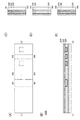
図1は、μ―PCD測定を行うための装置の一例を示す模式図である。図1に示す装置は、ワイドギャップ半導体の薄膜の評価に好適である。特に、トランジスタの半導体に用いられる、1nm以上1μm以下、2nm以上500nm以下、3nm以上200nm以下または5nm以上100nm以下の膜厚のワイドギャップ半導体の評価に好適である。 FIG. 1 is a schematic view showing an example of an apparatus for performing μ-PCD measurement. The apparatus shown in FIG. 1 is suitable for evaluating a thin film of a wide-gap semiconductor. In particular, it is suitable for evaluation of wide-gap semiconductors having a film thickness of 1 nm or more and 1 μm or less, 2 nm or more and 500 nm or less, 3 nm or more and 200 nm or less, or 5 nm or more and 100 nm or less, which are used for transistor semiconductors.
図1に示す装置は、パルスレーザ発振器1301と、マイクロ波発振器1302と、方向性結合器1303と、導波管1305と、ミキサー1306と、信号処理装置1307と、試料ステージ1311と、を有する。なお、図1において、導波管1305は、コーナー部が曲率を有する形状を示しているが、これに限定されるものではない。試料ステージ1311上には、試料1320を配置できる。試料1320は、例えば、基板1320bと、基板1320b上の酸化物半導体1320aと、を有する。
The apparatus shown in FIG. 1 includes a
試料ステージ1311の上面には、導電体が配置されている。導電体としては、アルミニウム、チタン、クロム、マンガン、鉄、コバルト、ニッケル、銅、亜鉛、ガリウム、イットリウム、ジルコニウム、モリブデン、ルテニウム、銀、インジウム、スズ、タンタル若しくはタングステンを一種以上、又は該金属元素の一種以上及びホウ素、窒素、酸素、フッ素、シリコン若しくはリンの一種以上含む導電体を、単層で、または積層で用いればよい。例えば、ステンレス鋼などの合金や化合物であってもよく、アルミニウムを含む導電体、銅及びチタンを含む導電体、銅及びマンガンを含む導電体、インジウム、スズ及び酸素を含む導電体、チタン及び窒素を含む導電体などを用いてもよい。
A conductor is arranged on the upper surface of the
なお、試料1320と試料ステージ1311との間にスペーサ1310を配置しても構わない。スペーサ1310は、マグネシウム、アルミニウム、シリコン、ガリウム、ゲルマニウム、イットリウム、ジルコニウム、ランタン、ネオジム、ハフニウム又はタンタルの一種以上及びアルゴン、ホウ素、炭素、窒素、酸素、フッ素、リン又は塩素の一種以上を含む絶縁体を、単層で、または積層で用いればよい。例えば、酸化アルミニウム、酸化マグネシウム、酸化シリコン、酸化窒化シリコン、窒化酸化シリコン、窒化シリコン、酸化ガリウム、酸化ゲルマニウム、酸化イットリウム、酸化ジルコニウム、酸化ランタン、酸化ネオジム、酸化ハフニウムまたは酸化タンタルを用いればよい。なお、酸化窒化シリコン膜とは、その組成として、窒素よりも酸素の含有量が多い膜を指し、窒化酸化シリコン膜とは、その組成として、酸素よりも窒素の含有量が多い膜を指す。
The
スペーサ1310は、例えば、酸化物半導体1320aの上面と、試料ステージ1311の上面と、の距離が基板1320b及びスペーサ1310におけるマイクロ波の波長の1/4程度となるように厚さを選択すればよい。なお、スペーサ1310を配置することにより、試料1320を上下逆さまに配置した場合でも評価が可能となる場合がある。試料1320を上下逆さまに配置することで、例えば、基板1320bと酸化物半導体1320aとの界面の影響を多く含んだ情報が得られる場合がある。
The thickness of the
以下に、酸化物半導体1320aのμ―PCD測定による評価方法を示す。
The evaluation method of the
まず、マイクロ波発振器1302より、マイクロ波を放射する。放射されたマイクロ波を特に進行波(入射波ともいう。)と呼ぶ。方向性結合器1303を介して進行波が、導波管1305と位相器1315とに分かれる。導波管1305を通った進行波は、試料1320に入射する。このとき、試料1320の酸化物半導体1320aで反射したマイクロ波(特に反射波と呼ぶ。)が、再び導波管1305を通る。反射波は、ミキサー1306にて、位相器1315を介して分かれた進行波と混合される。混合された信号は、信号処理装置1307において検出される。
First, microwaves are radiated from the
このとき、信号処理装置1307で検出される信号の強度は、酸化物半導体1320aにおけるマイクロ波の反射強度によって変化する。例えば、酸化物半導体1320aのキャリア密度が高いほど、酸化物半導体1320aの導電率が高くなる。導電率が高くなると、マイクロ波の反射強度は高くなり、それに伴って信号処理装置1307で検出される信号の強度も強くなる。
At this time, the signal intensity detected by the
また、酸化物半導体1320aは、励起光を吸収することで正孔及び電子を生成する。即ち、励起光を酸化物半導体1320aに照射することで、酸化物半導体1320aのキャリア密度が高くなり、それに伴いマイクロ波の反射強度が高くなる。なお、励起光は、ミラー1313及びレンズ1314を介して酸化物半導体1320aに照射させればよい。
Further, the
ある程度の時間、酸化物半導体1320aに励起光を当て続けると、マイクロ波の反射強度は、励起光によるキャリアの生成と、再結合などによるキャリアの消失と、のバランスによって一定値をとる。この値が、マイクロ波の反射強度の最も高い値となることから、マイクロ波の反射強度のピーク値と呼ぶことができる。
When the
なお、励起光としては、例えば、パルスレーザ発振器1301から放射されたレーザ光を用いることができる。レーザ光は、酸化物半導体1320aのバンドギャップよりも十分に高いエネルギーの波長を用いると好ましい。また、光学系のコストの上昇を抑えるためには、レーザ光の波長は200nm以上が好ましい。ただし、波長が200nm未満のレーザ光を用いても構わない。なお、光の進入長は、光の強度が1/eに減衰する深さであり、数式1で表すことができる。
As the excitation light, for example, a laser beam emitted from the

ここで、dは光の進入長、λは光の波長、kは減衰係数を示す。 Here, d is the penetration length of light, λ is the wavelength of light, and k is the attenuation coefficient.
例えば、酸化物半導体1320aのバンドギャップよりも十分に高いエネルギーの波長の励起光を用いない場合、検出感度を高めるために励起光の出力をある程度高くしなくてはならない。そのため、酸化物半導体1320aを変質させてしまう場合がある。酸化物半導体1320aのバンドギャップよりも十分に高いエネルギーの波長の励起光を用いることで、励起光の出力を小さくした場合でも酸化物半導体1320aのキャリア密度を十分に高くできる。したがって、上述したような、酸化物半導体1320aの変質を抑制できる。
For example, when excitation light having a wavelength having a wavelength sufficiently higher than the band gap of the
また、酸化物半導体1320aへの進入長の浅い励起光を用いることで、基板1320bなど下地の情報が測定結果に反映されることを抑制できる。また、干渉効果により、酸化物半導体1320aの厚さに応じて測定結果にムラが生じることを抑制できる。
Further, by using the excitation light having a shallow penetration length into the
基板1320bとして、μ―PCD測定での励起光のエネルギーよりもバンドギャップが小さい基板を用いる場合、励起光照射によって基板にキャリアが多数発生する。このような試料のμ―PCD測定を行うと、基板1320b由来の信号が大きくなり、酸化物半導体1320a由来の信号を打ち消す場合がある。そのため、励起光のエネルギーよりもバンドギャップが大きい基板、例えば、ガラスや石英を用いることが望ましい。
When a substrate having a bandgap smaller than the energy of the excitation light in the μ-PCD measurement is used as the
酸化物半導体1320aの上または下に、μ―PCD測定での励起光のエネルギーよりもバンドギャップが大きい膜を有する場合においても、酸化物半導体1320a由来の信号を検出できる。例えばシリコン酸化膜は、励起光よりバンドギャップが大きく、キャリアが発生しづらいことから、μ―PCD測定においてシリコン酸化膜由来の信号は小さくなり、酸化物半導体1320a由来の信号を検出できる。なお、酸化物半導体1320aの上または下に設ける、μ―PCD測定での励起光のエネルギーよりもバンドギャップが大きい膜は、積層構造としてもよい。
Even when a film having a bandgap larger than the energy of the excitation light in the μ-PCD measurement is provided above or below the
酸化物半導体1320aへの励起光の照射を止めると、キャリアの生成が止まり、酸化物半導体1320aのキャリア密度は減衰していく。酸化物半導体において、励起光の照射により生成したキャリアは単純に指数関数的に減衰するのではなく、減衰の途中から減衰が緩やかになる場合がある。つまり、キャリアの減衰は、速やかに減衰する成分と緩やかに減衰する成分の二つから構成される。速やかに減衰する成分はおおよそ指数関数的であり、緩やかに減衰する成分は非指数関数型の傾向となる場合がある。キャリア密度の減衰は、速やかな減衰成分に対する指数関数型モデルと、緩やかな減衰成分に対する拡張指数関数型モデルを組み合わせた数式2で表すことができる。
When the irradiation of the
ここで、tは励起光の照射を停止してからの時間、n(t)は時間tにおけるキャリア密度、n0は励起光照射下でのキャリア密度、τ1は速やかに減衰する成分の時定数、τ2は緩やかに減衰する成分の時定数、βは拡張指数係数を示す。 Here, t is the time after the irradiation of the excitation light is stopped, n (t) is the carrier density at the time t, n 0 is the carrier density under the irradiation of the excitation light, and τ1 is the time constant of the component that rapidly attenuates. , Τ2 is the time constant of the slowly decaying component, and β is the extended exponential coefficient.
本明細書では、速やかに減衰する成分の時定数をライフタイムτ1、緩やかに減衰する成分の時定数をライフタイムτ2と呼ぶ。 In the present specification, the time constant of the rapidly decaying component is referred to as lifetime τ1, and the time constant of the slowly decaying component is referred to as lifetime τ2.
酸化物半導体1320aに照射されたマイクロ波は、酸化物半導体1320aのキャリア密度で決まる導電率に基づいたマイクロ波の反射強度で反射される。つまり、酸化物半導体1320aのキャリア密度とマイクロ波の反射強度が対応することから、マイクロ波の反射強度の減衰を、数式3で表すことができる。なお、μ―PCD測定によるライフタイムτ1及びライフタイムτ2の算出方法は、S. Yasuno, et al.: Journal of Applied Physics 2012 vol.112, 053715の記載を参照できる。
The microwave irradiated on the
ここで、tは励起光の照射を停止してからの時間、R(t)は時間tにおけるマイクロ波の反射強度、R0は励起光照射下でのマイクロ波の反射強度、τ1は速やかに減衰する成分のライフタイム、τ2は緩やかに減衰する成分のライフタイム、βは拡張指数関数を示す。 Here, t is the time after the irradiation of the excitation light is stopped, R (t) is the reflection intensity of the microwave at time t, R 0 is the reflection intensity of the microwave under the irradiation of the excitation light, and τ1 is promptly. The lifetime of the decaying component, τ2 is the lifetime of the slowly decaying component, and β is the extended exponential function.
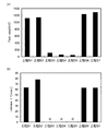
μ―PCD測定で得られる減衰曲線の例を図3(A)に示す。図3(A)は、横軸に励起光の照射を停止してからの時間[nsec]をとり、左の縦軸にマイクロ波の反射強度[mV]をとる。プロットは実測値を示し、実線は数式3を用いたフィッティングから得られた速やかに減衰する成分、破線はフィッティングから得られた緩やかに減衰する成分を示す。このように、得られたマイクロ波の反射強度の減衰曲線から、キャリアのライフタイムτ1及びτ2を算出できる。
An example of the attenuation curve obtained by μ-PCD measurement is shown in FIG. 3 (A). In FIG. 3A, the horizontal axis represents the time [nsec] after the irradiation of the excitation light is stopped, and the left vertical axis represents the reflection intensity [mV] of the microwave. The plot shows the measured values, the solid line shows the rapidly decaying component obtained from the
マイクロ波の反射強度が非常に低い例を図3(B)に示す。図3(B)は、横軸に励起光の照射を停止してからの時間[nsec]をとり、左の縦軸にマイクロ波の反射強度[mV]をとる。このように、マイクロ波の反射強度が低い試料においては、減衰曲線のノイズの影響が大きくなり、ライフタイムτ1及びτ2を算出できない場合がある。 An example in which the reflection intensity of microwaves is very low is shown in FIG. 3 (B). In FIG. 3B, the horizontal axis represents the time [nsec] after the irradiation of the excitation light is stopped, and the left vertical axis represents the reflection intensity [mV] of the microwave. As described above, in a sample having a low microwave reflection intensity, the influence of noise on the attenuation curve becomes large, and the lifetimes τ1 and τ2 may not be calculated.
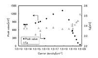
酸化物半導体の伝導帯が縮退していない範囲においては、酸化物半導体のキャリア密度が高くなるほど、μ―PCD測定で得られる反射強度のピーク値が高くなり、また、ライフタイムが長くなる傾向となる。キャリア密度とピーク値、ライフタイムの相関関係を事前に取得しておくことで、任意の酸化物半導体のμ―PCD測定を行うことにより、該酸化物半導体のキャリア密度を推測できる。 In the range where the conduction band of the oxide semiconductor is not degenerated, the higher the carrier density of the oxide semiconductor, the higher the peak value of the reflection intensity obtained by μ-PCD measurement, and the longer the lifetime tends to be. Become. By acquiring the correlation between the carrier density, the peak value, and the lifetime in advance, the carrier density of the oxide semiconductor can be estimated by performing the μ-PCD measurement of any oxide semiconductor.
酸化物半導体をトランジスタに用いる場合、良好なトランジスタの電気特性を得るには、酸化物半導体のキャリア密度の制御が重要となる。μ―PCD測定を行うことにより、酸化物半導体のキャリア密度を推測できることから、効率良く、トランジスタの電気特性の向上が可能となる。具体的には、しきい値電圧のマイナスシフトの抑制、オン電流の向上、または電界効果移動度の向上が可能となる。 When an oxide semiconductor is used for a transistor, it is important to control the carrier density of the oxide semiconductor in order to obtain good electrical characteristics of the transistor. Since the carrier density of the oxide semiconductor can be estimated by performing the μ-PCD measurement, it is possible to efficiently improve the electrical characteristics of the transistor. Specifically, it is possible to suppress the negative shift of the threshold voltage, improve the on-current, or improve the field effect mobility.
さらにキャリア密度が高くなり、伝導帯が縮退する範囲になると、キャリア密度が高くなるほど、μ―PCD測定で得られるピーク値は低くなる。また、酸化物半導体の伝導帯が縮退する範囲においては、キャリア密度が高くなるほど、μ―PCD測定で得られるライフタイムが短くなる。さらにキャリア密度が高くなると、ピーク値が低くなることから、図3(B)に示したように、減衰曲線のノイズの影響が大きくなり、ライフタイムを算出できなくなる。ピーク値と合わせて、ライフタイムも用いることにより、酸化物半導体のキャリア密度をより精度良く推測できる。 Further, when the carrier density becomes higher and the conduction band degenerates, the higher the carrier density, the lower the peak value obtained by the μ-PCD measurement. Further, in the range where the conduction band of the oxide semiconductor is degenerated, the higher the carrier density, the shorter the lifetime obtained by the μ-PCD measurement. As the carrier density increases, the peak value decreases, and as shown in FIG. 3B, the influence of noise on the attenuation curve increases, making it impossible to calculate the lifetime. By using the lifetime together with the peak value, the carrier density of the oxide semiconductor can be estimated more accurately.
縮退領域において、キャリア密度が高くなるほどピーク値が低くなる原因として、次の3つが考えられる。一つ目は、キャリア―キャリア散乱による移動度の低下である。二つ目は、キャリア―キャリア散乱による、励起光照射下でのキャリア密度の減少である。三つ目は、バースタイン・モスシフト(Burstein―Moss shift)効果による、励起光照射下でのキャリア密度の減少である。 In the degenerate region, there are three possible causes for the peak value to decrease as the carrier density increases. The first is a decrease in mobility due to carrier-carrier scattering. The second is the decrease in carrier density under excitation light irradiation due to carrier-carrier scattering. The third is a decrease in carrier density under excitation light irradiation due to the Burstein-Mossshift effect.
まず、一つ目及び二つ目の理由について説明する。励起光照射により過剰キャリアが生成し、酸化物半導体の導電率が増加する。励起光照射による導電率の変化量を、数式4で表すことができる。
First, the first and second reasons will be described. Excess carriers are generated by irradiation with excitation light, and the conductivity of the oxide semiconductor increases. The amount of change in conductivity due to excitation light irradiation can be expressed by
![]()
![]()
ここで、Δσは励起光照射による導電率の変化量、qは電気素量、μnは電子の移動度、ndarkは励起光照射前のキャリア密度、nphotoは励起光照射下でのキャリア密度を示す。 Here, Δσ is the amount of change in conductivity due to excitation light irradiation, q is the elementary charge, μ n is the electron mobility, n dark is the carrier density before excitation light irradiation, and n photo is the carrier under excitation light irradiation. Indicates density.
キャリア密度が高くなると、キャリア―キャリア散乱により移動度μnが低下することから、励起光照射による導電率の変化量が小さくなることが分かる。また、キャリア密度が高くなると、キャリア―キャリア散乱によりライフタイムが短くなり、励起光照射下でのキャリア密度nphotoが減少することから、励起光照射による導電率の変化量が小さくなることが分かる。よって、μ―PCD測定のピーク値が小さくなると考えられる。 As the carrier density increases, the mobility μ n decreases due to carrier-carrier scattering, so it can be seen that the amount of change in conductivity due to excitation light irradiation decreases. Further, when the carrier density is high, the lifetime is shortened due to carrier-carrier scattering, and the carrier density nphoto under excitation light irradiation is reduced, so that the amount of change in conductivity due to excitation light irradiation is small. .. Therefore, it is considered that the peak value of the μ-PCD measurement becomes small.
次に、三つ目の理由について説明する。キャリア密度が高くなり、伝導帯が縮退すると、光学バンドギャップが広がることが知られており、これはバースタイン・モスシフト(Burstein―Moss shift)効果と呼ばれる。光学バンドギャップが広がることにより、励起光照射で励起するキャリア密度が減少し、μ―PCD測定のピーク値が小さくなると考えられる。 Next, the third reason will be explained. It is known that the optical bandgap widens as the carrier density increases and the conduction band degenerates, which is called the Bernstein-Mossshift effect. It is considered that the widening of the optical band gap reduces the carrier density excited by the excitation light irradiation and reduces the peak value of the μ-PCD measurement.
酸化物半導体のキャリア密度測定方法の一つとして、ホール(Hall)効果測定が挙げられる。しかし、ホール(Hall)効果測定は、測定可能なサンプルサイズが小さい為、基板サイズが大きいと、基板を分断する必要がある。また、サンプルに針を接触させて測定する。ホール効果測定は破壊、接触測定になることから、例えば酸化物半導体を用いたトランジスタ作製工程において、ホール効果測定を工程管理に用いるのは好ましくない。 One of the methods for measuring the carrier density of an oxide semiconductor is the Hall effect measurement. However, in the Hall effect measurement, since the measurable sample size is small, if the substrate size is large, it is necessary to divide the substrate. In addition, the needle is brought into contact with the sample for measurement. Since the Hall effect measurement is fracture and contact measurement, it is not preferable to use the Hall effect measurement for process control in, for example, a transistor manufacturing process using an oxide semiconductor.
これに対して、μ―PCD測定は酸化物半導体を形成した後であれば、トランジスタ作製の工程途中に非接触、非破壊、短時間で酸化物半導体のキャリア密度を評価できる。 On the other hand, in the μ-PCD measurement, the carrier density of the oxide semiconductor can be evaluated in a non-contact, non-destructive, and short time during the transistor manufacturing process after the oxide semiconductor is formed.
また、トランジスタを作製する場合、チャネル、ソース、ドレイン、ゲートなどを形成するまで電気特性の測定を行うことができない。しかし、μ―PCD測定は工程途中に非接触、非破壊、短時間で酸化物半導体のキャリア密度を評価し、当該キャリア密度からトランジスタの電気特性を推測することができる。このように、工程途中に適宜μ―PCD測定を行うことにより、工程不良を容易に発見でき、μ−PCD測定結果を効率良く工程管理へフィードバックすることができる。 Further, when a transistor is manufactured, the electrical characteristics cannot be measured until a channel, a source, a drain, a gate, or the like is formed. However, in the μ-PCD measurement, the carrier density of the oxide semiconductor can be evaluated in a non-contact, non-destructive, and short time during the process, and the electrical characteristics of the transistor can be estimated from the carrier density. In this way, by appropriately performing μ-PCD measurement during the process, process defects can be easily found, and the μ-PCD measurement result can be efficiently fed back to process management.
よって、トランジスタ作製工程途中にμ―PCD測定を行うことにより、時間遅延なく異常工程を確認でき、即座に異常に対応できる。また、異常のあった試料をトランジスタ製造工程から外すことにより、後の工程を流す無駄を排除できる。その為、効率良く、トランジスタを歩留まり高く作製できる。または、トランジスタを生産性高く作製できる。または、効率良く、該トランジスタを有する半導体装置を生産性高く作製できる。 Therefore, by performing the μ-PCD measurement in the middle of the transistor manufacturing process, the abnormal process can be confirmed without a time delay, and the abnormal can be dealt with immediately. Further, by removing the abnormal sample from the transistor manufacturing process, it is possible to eliminate the waste of flowing the subsequent process. Therefore, the transistor can be efficiently manufactured with a high yield. Alternatively, the transistor can be manufactured with high productivity. Alternatively, a semiconductor device having the transistor can be efficiently manufactured with high productivity.
また、試料ステージ1311をX方向及びY方向に動かすことで、酸化物半導体1320aの面内において、複数個所の評価を行うことができる。μ―PCD測定は非接触、非破壊、短時間で試料面内の複数個所の測定が可能である。したがって、トランジスタ作製工程途中で試料面内の複数個所でμ―PCD測定を行うことにより、工程途中で酸化物半導体のキャリア密度の面内分布を評価し、当該キャリア密度からトランジスタの電気特性の面内分布を推測することができる。したがって、試料面内分布に異常が発生した場合でも、速やか工程管理へフィードバックすることができる。
Further, by moving the
なお、酸化物半導体の膜厚やバンドギャップにより、酸化物半導体のμ―PCD測定での励起光の吸収率は異なる。励起光の吸収率が異なると、酸化物半導体に発生するキャリア密度が異なる為、酸化物半導体の膜厚やバンドギャップにより、マイクロ波の反射強度のピーク値が異なる。トランジスタ作製に用いる酸化物半導体の膜厚やバンドギャップに合わせたサンプルを作製し、事前にホール(Hall)効果測定などによるキャリア密度と、μ―PCD測定によるピーク値及びライフタイムとの相関を取得しておくことで、より精度良く、キャリア密度を推測することができる。 The absorption rate of excitation light in the μ-PCD measurement of the oxide semiconductor differs depending on the film thickness and band gap of the oxide semiconductor. If the absorption rate of the excitation light is different, the carrier density generated in the oxide semiconductor is different, so that the peak value of the microwave reflection intensity is different depending on the film thickness and band gap of the oxide semiconductor. Prepare a sample that matches the film thickness and band gap of the oxide semiconductor used for transistor fabrication, and obtain the correlation between the carrier density by Hall effect measurement and the peak value and lifetime by μ-PCD measurement in advance. By doing so, the carrier density can be estimated more accurately.
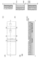
また、図2のように、導波管1305a及び導波管1305bの二つの導波管と、マジックT1304と、有する装置を用いても構わない。なお、導波管1305aと導波管1305bとが、対称性を有すると好ましい。または、導波管1305aと導波管1305bとのマイクロ波の経路長が同じであればよい。なお、図2において、導波管1305a及び導波管1305bは、コーナー部が曲率を有する形状を示しているが、これに限定されるものではない。
Further, as shown in FIG. 2, a device having two waveguides, a
図2の場合も、まず、マイクロ波発振器1302より、マイクロ波を放射する。方向性結合器1303を介して進行波が、マジックT1304と位相器1315とに分かれる。マジックT1304において、進行波は、導波管1305a及び導波管1305bに分かれる。導波管1305aを通った進行波は、励起光とともに試料1320に入射する。また、導波管1305bを通った進行波は、そのまま試料1320に入射する。このとき、試料1320の酸化物半導体1320aで反射したマイクロ波が、再び導波管1305a及び導波管1305bを通り、マジックT1304に戻る。導波管1305aと導波管1305bと、を通った反射波は、マジックT1304において再び合流する、そして、マジックT1304はそれらの差信号を出力する。そして、ミキサー1306にて、位相器1315を介して分かれた進行波と混合される。混合された信号は、信号処理装置1307において検出される。
Also in the case of FIG. 2, first, microwaves are radiated from the
このとき、導波管1305bを通った反射波は、マイクロ波発振器1302に起因したノイズ、及び機械的振動による外乱などを、導波管1305aを通った反射波と同じだけ含む。したがって、その差信号をとることで、ノイズなどの影響を低減させられる。そのため、図2に示す装置は、励起光によるマイクロ波の反射強度の変化を、さらに感度よく検出できる。
At this time, the reflected wave passing through the
(実施の形態2)
本実施の形態においては、本発明の一態様に用いることのできる、酸化物半導体の組成、及び酸化物半導体の構造等について、図4及び図5を参照して説明する。
(Embodiment 2)
In the present embodiment, the composition of the oxide semiconductor, the structure of the oxide semiconductor, and the like that can be used in one aspect of the present invention will be described with reference to FIGS. 4 and 5.
[酸化物半導体]
以下に、本発明に係る酸化物半導体について説明する。
[Oxide semiconductor]
The oxide semiconductor according to the present invention will be described below.
酸化物半導体は、少なくともインジウムまたは亜鉛を含むことが好ましい。特にインジウム及び亜鉛を含むことが好ましい。また、それらに加えて、アルミニウム、ガリウム、イットリウムまたはスズなどが含まれていることが好ましい。また、ホウ素、シリコン、チタン、鉄、ニッケル、ゲルマニウム、ジルコニウム、モリブデン、ランタン、セリウム、ネオジム、ハフニウム、タンタル、タングステン、またはマグネシウムなどから選ばれた一種、または複数種が含まれていてもよい。 The oxide semiconductor preferably contains at least indium or zinc. In particular, it preferably contains indium and zinc. In addition to them, aluminum, gallium, yttrium, tin and the like are preferably contained. It may also contain one or more selected from boron, silicon, titanium, iron, nickel, germanium, zirconium, molybdenum, lanthanum, cerium, neodymium, hafnium, tantalum, tungsten, magnesium and the like.
ここでは、酸化物半導体が、インジウム、元素M及び亜鉛を有するInMZnOである場合を考える。なお、元素Mは、アルミニウム、ガリウム、イットリウムまたはスズなどとする。そのほかの元素Mに適用可能な元素としては、ホウ素、シリコン、チタン、鉄、ニッケル、ゲルマニウム、ジルコニウム、モリブデン、ランタン、セリウム、ネオジム、ハフニウム、タンタル、タングステン、マグネシウムなどがある。ただし、元素Mとして、前述の元素を複数組み合わせても構わない場合がある。 Here, consider the case where the oxide semiconductor is InMZnO having indium, element M, and zinc. The element M is aluminum, gallium, yttrium, tin, or the like. Examples of elements applicable to the other element M include boron, silicon, titanium, iron, nickel, germanium, zirconium, molybdenum, lanthanum, cerium, neodymium, hafnium, tantalum, tungsten, and magnesium. However, as the element M, a plurality of the above-mentioned elements may be combined in some cases.
<構造>
酸化物半導体は、単結晶酸化物半導体と、それ以外の非単結晶酸化物半導体と、に分けられる。非単結晶酸化物半導体としては、例えば、CAAC−OS(c−axis aligned crystalline oxide semiconductor)、多結晶酸化物半導体、nc−OS(nanocrystalline oxide semiconductor)、擬似非晶質酸化物半導体(a−like OS:amorphous−like oxide semiconductor)及び非晶質酸化物半導体などがある。
<Structure>
Oxide semiconductors are divided into single crystal oxide semiconductors and other non-single crystal oxide semiconductors. Examples of the non-single crystal oxide semiconductor include CAAC-OS (c-axis aligned semiconductor semiconductor), polycrystalline oxide semiconductor, nc-OS (nanocrystalline oxide semiconductor), and pseudo-amorphous oxide semiconductor (a-lique). OS: atomous-like oxide semiconductor) and amorphous oxide semiconductors.
CAAC−OSは、c軸配向性を有し、かつa−b面方向において複数のナノ結晶が連結し、歪みを有した結晶構造となっている。なお、歪みとは、複数のナノ結晶が連結する領域において、格子配列の揃った領域と、別の格子配列の揃った領域と、の間で格子配列の向きが変化している箇所を指す。 CAAC-OS has a c-axis orientation and has a distorted crystal structure in which a plurality of nanocrystals are connected in the ab plane direction. The strain refers to a region where the orientation of the lattice arrangement changes between a region in which the lattice arrangement is aligned and a region in which another lattice arrangement is aligned in the region where a plurality of nanocrystals are connected.
ナノ結晶は、六角形を基本とするが、正六角形状とは限らず、非正六角形状である場合がある。また、歪みにおいて、五角形、及び七角形などの格子配列を有する場合がある。なお、CAAC−OSにおいて、歪み近傍においても、明確な結晶粒界(グレインバウンダリーともいう)を確認することはできない。即ち、格子配列の歪みによって、結晶粒界の形成が抑制されていることがわかる。これは、CAAC−OSが、a−b面方向において原子配列が稠密でないことや、金属元素が置換することで原子間の結合距離が変化することなどによって、歪みを許容することができるためと考えられる。 Although nanocrystals are basically hexagonal, they are not limited to regular hexagons and may have non-regular hexagons. Further, in the strain, it may have a lattice arrangement such as a pentagon and a heptagon. In CAAC-OS, a clear grain boundary (also referred to as grain boundary) cannot be confirmed even in the vicinity of strain. That is, it can be seen that the formation of grain boundaries is suppressed by the distortion of the lattice arrangement. This is because CAAC-OS can tolerate distortion due to the fact that the atomic arrangement is not dense in the ab plane direction and the bond distance between atoms changes due to the substitution of metal elements. Conceivable.
また、CAAC−OSは、インジウム、及び酸素を有する層(以下、In層)と、元素M、亜鉛、及び酸素を有する層(以下、(M,Zn)層)とが積層した、層状の結晶構造(層状構造ともいう)を有する傾向がある。なお、インジウムと元素Mは、互いに置換可能であり、(M,Zn)層の元素Mがインジウムと置換した場合、(In,M,Zn)層と表すこともできる。また、In層のインジウムが元素Mと置換した場合、(In,M)層と表すこともできる。 Further, CAAC-OS is a layered crystal in which a layer having indium and oxygen (hereinafter, In layer) and a layer having elements M, zinc, and oxygen (hereinafter, (M, Zn) layer) are laminated. It tends to have a structure (also called a layered structure). Indium and the element M can be replaced with each other, and when the element M of the (M, Zn) layer is replaced with indium, it can be expressed as the (In, M, Zn) layer. Further, when the indium of the In layer is replaced with the element M, it can be expressed as the (In, M) layer.
nc−OSは、微小な領域(例えば、1nm以上10nm以下の領域、特に1nm以上3nm以下の領域)において原子配列に周期性を有する。また、nc−OSは、異なるナノ結晶間で結晶方位に規則性が見られない。そのため、膜全体で配向性が見られない。したがって、nc−OSは、分析方法によっては、a−like OSや非晶質酸化物半導体と区別が付かない場合がある。 The nc-OS has periodicity in the atomic arrangement in a minute region (for example, a region of 1 nm or more and 10 nm or less, particularly a region of 1 nm or more and 3 nm or less). In addition, nc-OS does not show regularity in crystal orientation between different nanocrystals. Therefore, no orientation is observed in the entire film. Therefore, the nc-OS may be indistinguishable from the a-like OS and the amorphous oxide semiconductor depending on the analysis method.
a−like OSは、nc−OSと非晶質酸化物半導体との間の構造を有する酸化物半導体である。a−like OSは、鬆または低密度領域を有する。即ち、a−like OSは、nc−OS及びCAAC−OSと比べて、結晶性が低い。 The a-like OS is an oxide semiconductor having a structure between nc-OS and an amorphous oxide semiconductor. The a-like OS has a void or low density region. That is, a-like OS has lower crystallinity than nc-OS and CAAC-OS.
酸化物半導体は、多様な構造をとり、それぞれが異なる特性を有する。本発明の一態様の酸化物半導体は、非晶質酸化物半導体、多結晶酸化物半導体、a−like OS、nc−OS、CAAC−OSのうち、二種以上を有していてもよい。 Oxide semiconductors have various structures, and each has different characteristics. The oxide semiconductor of one aspect of the present invention may have two or more of amorphous oxide semiconductor, polycrystalline oxide semiconductor, a-like OS, nc-OS, and CAAC-OS.
<原子数比>
次に、図4(A)、図4(B)、及び図4(C)を用いて、本発明に係る酸化物半導体が有するインジウム、元素M及び亜鉛の原子数比の好ましい範囲について説明する。なお、図4(A)、図4(B)、及び図4(C)には、酸素の原子数比については記載しない。また、酸化物半導体が有するインジウム、元素M、及び亜鉛の原子数比のそれぞれの項を[In]、[M]、及び[Zn]とする。
<Atomic number ratio>
Next, with reference to FIGS. 4 (A), 4 (B), and 4 (C), a preferable range of atomic number ratios of indium, element M, and zinc contained in the oxide semiconductor according to the present invention will be described. .. Note that FIG. 4 (A), FIG. 4 (B), and FIG. 4 (C) do not describe the atomic number ratio of oxygen. Further, the respective terms of the atomic number ratios of indium, element M, and zinc contained in the oxide semiconductor are [In], [M], and [Zn].
図4(A)、図4(B)、及び図4(C)において、破線は、[In]:[M]:[Zn]=(1+α):(1−α):1の原子数比(−1≦α≦1)となるライン、[In]:[M]:[Zn]=(1+α):(1−α):2の原子数比となるライン、[In]:[M]:[Zn]=(1+α):(1−α):3の原子数比となるライン、[In]:[M]:[Zn]=(1+α):(1−α):4の原子数比となるライン、及び[In]:[M]:[Zn]=(1+α):(1−α):5の原子数比となるラインを表す。 In FIGS. 4 (A), 4 (B), and 4 (C), the broken line indicates the atomic number ratio of [In]: [M]: [Zn] = (1 + α) :( 1-α): 1. Line where (-1 ≤ α ≤ 1), [In]: [M]: [Zn] = (1 + α): (1-α): Line where the atomic number ratio is 2, [In]: [M] : [Zn] = (1 + α): (1-α): A line having an atomic number ratio of 3, [In]: [M]: [Zn] = (1 + α): (1-α): 4 atomic numbers It represents a line having a ratio and a line having an atomic number ratio of [In]: [M]: [Zn] = (1 + α) :( 1-α): 5.
また、一点鎖線は、[In]:[M]:[Zn]=5:1:βの原子数比(β≧0)となるライン、[In]:[M]:[Zn]=2:1:βの原子数比となるライン、[In]:[M]:[Zn]=1:1:βの原子数比となるライン、[In]:[M]:[Zn]=1:2:βの原子数比となるライン、[In]:[M]:[Zn]=1:3:βの原子数比となるライン、及び[In]:[M]:[Zn]=1:4:βの原子数比となるラインを表す。 The one-point chain line is a line having an atomic number ratio of [In]: [M]: [Zn] = 5: 1: β (β ≧ 0), [In]: [M]: [Zn] = 2: Line with an atomic number ratio of 1: β, [In]: [M]: [Zn] = 1: 1: Line with an atomic number ratio of β, [In]: [M]: [Zn] = 1: 2: Atomic number ratio of β, [In]: [M]: [Zn] = 1: 3: β atomic number ratio, and [In]: [M]: [Zn] = 1 : Represents a line having an atomic number ratio of 4: β.
また、図4(A)、図4(B)、及び図4(C)に示す、[In]:[M]:[Zn]=0:2:1の原子数比、及びその近傍値の酸化物半導体は、スピネル型の結晶構造をとりやすい。 Further, the atomic number ratio of [In]: [M]: [Zn] = 0: 2: 1 and its vicinity values shown in FIGS. 4 (A), 4 (B), and 4 (C). Oxide semiconductors tend to have a spinel-type crystal structure.
また、酸化物半導体中に複数の相が共存する場合がある(二相共存、三相共存など)。例えば、原子数比が[In]:[M]:[Zn]=0:2:1の近傍値である場合、スピネル型の結晶構造と層状の結晶構造との二相が共存しやすい。また、原子数比が[In]:[M]:[Zn]=1:0:0の近傍値である場合、ビックスバイト型の結晶構造と層状の結晶構造との二相が共存しやすい。酸化物半導体中に複数の相が共存する場合、異なる結晶構造の間において、結晶粒界が形成される場合がある。 In addition, a plurality of phases may coexist in the oxide semiconductor (two-phase coexistence, three-phase coexistence, etc.). For example, when the atomic number ratio is in the vicinity of [In]: [M]: [Zn] = 0: 2: 1, two phases of a spinel-type crystal structure and a layered crystal structure tend to coexist. Further, when the atomic number ratio is in the vicinity of [In]: [M]: [Zn] = 1: 0: 0, two phases of a big bite-type crystal structure and a layered crystal structure tend to coexist. When a plurality of phases coexist in an oxide semiconductor, grain boundaries may be formed between different crystal structures.
図4(A)に示す領域Aは、酸化物半導体が有する、インジウム、元素M、及び亜鉛の原子数比の好ましい範囲の一例について示している。 The region A shown in FIG. 4A shows an example of a preferable range of atomic number ratios of indium, element M, and zinc contained in the oxide semiconductor.
酸化物半導体は、インジウムの含有率を高くすることで、酸化物半導体のキャリア移動度(電子移動度)を高くすることができる。従って、インジウムの含有率が高い酸化物半導体はインジウムの含有率が低い酸化物半導体と比較してキャリア移動度が高くなる。 By increasing the indium content of the oxide semiconductor, the carrier mobility (electron mobility) of the oxide semiconductor can be increased. Therefore, an oxide semiconductor having a high indium content has a higher carrier mobility than an oxide semiconductor having a low indium content.
一方、酸化物半導体中のインジウム及び亜鉛の含有率が低くなると、キャリア移動度が低くなる。従って、原子数比が[In]:[M]:[Zn]=0:1:0、及びその近傍値である場合(例えば図4(C)に示す領域C)は、絶縁性が高くなる。 On the other hand, when the content of indium and zinc in the oxide semiconductor is low, the carrier mobility is low. Therefore, when the atomic number ratio is [In]: [M]: [Zn] = 0: 1: 0 and its neighboring values (for example, region C shown in FIG. 4C), the insulating property is high. ..
従って、本発明の一態様の酸化物半導体は、キャリア移動度が高く、かつ、結晶粒界が少ない層状構造となりやすい、図4(A)の領域Aで示される原子数比を有することが好ましい。 Therefore, it is preferable that the oxide semiconductor of one aspect of the present invention has the atomic number ratio shown in the region A of FIG. 4A, which tends to have a layered structure having high carrier mobility and few grain boundaries. ..
特に、図4(B)に示す領域Bでは、領域Aの中でも、CAAC−OSとなりやすく、キャリア移動度も高い優れた酸化物半導体が得られる。 In particular, in the region B shown in FIG. 4B, an excellent oxide semiconductor that easily becomes CAAC-OS and has high carrier mobility can be obtained even in the region A.
CAAC−OSは結晶性の高い酸化物半導体である。一方、CAAC−OSは、明確な結晶粒界を確認することはできないため、結晶粒界に起因する電子移動度の低下が起こりにくいといえる。また、酸化物半導体の結晶性は不純物の混入や欠陥の生成などによって低下する場合があるため、CAAC−OSは不純物や欠陥(酸素欠損など)の少ない酸化物半導体ともいえる。従って、CAAC−OSを有する酸化物半導体は、物理的性質が安定する。そのため、CAAC−OSを有する酸化物半導体は熱に強く、信頼性が高い。 CAAC-OS is a highly crystalline oxide semiconductor. On the other hand, in CAAC-OS, since a clear crystal grain boundary cannot be confirmed, it can be said that a decrease in electron mobility due to the crystal grain boundary is unlikely to occur. Further, since the crystallinity of the oxide semiconductor may be lowered due to the mixing of impurities or the generation of defects, CAAC-OS can be said to be an oxide semiconductor having few impurities and defects (oxygen deficiency, etc.). Therefore, the oxide semiconductor having CAAC-OS has stable physical properties. Therefore, the oxide semiconductor having CAAC-OS is resistant to heat and has high reliability.
なお、領域Bは、[In]:[M]:[Zn]=4:2:3から4.1、及びその近傍値を含む。近傍値には、例えば、[In]:[M]:[Zn]=5:3:4が含まれる。また、領域Bは、[In]:[M]:[Zn]=5:1:6、及びその近傍値、及び[In]:[M]:[Zn]=5:1:7、及びその近傍値を含む。 The region B includes [In]: [M]: [Zn] = 4: 2: 3 to 4.1, and values in the vicinity thereof. The neighborhood value includes, for example, [In]: [M]: [Zn] = 5: 3: 4. Further, the region B includes [In]: [M]: [Zn] = 5: 1: 6 and its neighboring values, and [In]: [M]: [Zn] = 5: 1: 7 and its vicinity. Includes neighborhood values.
なお、酸化物半導体が有する性質は、原子数比によって一義的に定まらない。同じ原子数比であっても、形成条件により、酸化物半導体の性質が異なる場合がある。例えば、酸化物半導体をスパッタリング装置にて成膜する場合、ターゲットの原子数比からずれた原子数比の膜が形成される。また、成膜時の基板温度によっては、ターゲットの[Zn]よりも、膜の[Zn]が小さくなる場合がある。従って、図示する領域は、酸化物半導体が特定の特性を有する傾向がある原子数比を示す領域であり、領域A乃至領域Cの境界は厳密ではない。 The properties of oxide semiconductors are not uniquely determined by the atomic number ratio. Even if the atomic number ratio is the same, the properties of the oxide semiconductor may differ depending on the formation conditions. For example, when an oxide semiconductor is formed by a sputtering apparatus, a film having an atomic number ratio deviating from the target atomic number ratio is formed. Further, depending on the substrate temperature at the time of film formation, the [Zn] of the film may be smaller than the [Zn] of the target. Therefore, the region shown is a region showing an atomic number ratio in which the oxide semiconductor tends to have a specific characteristic, and the boundary between the region A and the region C is not strict.
[酸化物半導体を有するトランジスタ]
続いて、上記酸化物半導体をトランジスタに用いる場合について説明する。
[Transistor with oxide semiconductor]
Subsequently, a case where the oxide semiconductor is used for a transistor will be described.
なお、上記酸化物半導体をトランジスタに用いることで、結晶粒界におけるキャリア散乱等を減少させることができるため、高い電界効果移動度のトランジスタを実現することができる。また、信頼性の高いトランジスタを実現することができる。 By using the oxide semiconductor for the transistor, carrier scattering and the like at the grain boundaries can be reduced, so that a transistor with high field effect mobility can be realized. Moreover, a highly reliable transistor can be realized.
また、トランジスタには、キャリア密度の低い酸化物半導体を用いることが好ましい。酸化物半導体膜のキャリア密度を低くする場合においては、酸化物半導体膜中の不純物濃度を低くし、欠陥準位密度を低くすればよい。本明細書等において、不純物濃度が低く、欠陥準位密度の低いことを高純度真性または実質的に高純度真性と言う。 Further, it is preferable to use an oxide semiconductor having a low carrier density for the transistor. When the carrier density of the oxide semiconductor film is lowered, the impurity concentration in the oxide semiconductor film may be lowered to lower the defect level density. In the present specification and the like, a low impurity concentration and a low defect level density is referred to as high-purity intrinsic or substantially high-purity intrinsic.
また、高純度真性または実質的に高純度真性である酸化物半導体膜は、欠陥準位密度が低いため、トラップ準位密度も低くなる場合がある。 Further, since the oxide semiconductor film having high purity intrinsicity or substantially high purity intrinsicity has a low defect level density, the trap level density may also be low.
また、酸化物半導体のトラップ準位に捕獲された電荷は、消失するまでに要する時間が長く、あたかも固定電荷のように振る舞うことがある。そのため、トラップ準位密度の高い酸化物半導体にチャネル領域が形成されるトランジスタは、電気特性が不安定となる場合がある。 In addition, the charge captured at the trap level of the oxide semiconductor takes a long time to disappear, and may behave as if it were a fixed charge. Therefore, a transistor in which a channel region is formed in an oxide semiconductor having a high trap level density may have unstable electrical characteristics.
従って、トランジスタの電気特性を安定にするためには、酸化物半導体中の不純物濃度を低減することが有効である。また、酸化物半導体中の不純物濃度を低減するためには、近接する膜中の不純物濃度も低減することが好ましい。不純物としては、水素、窒素、アルカリ金属、アルカリ土類金属、鉄、ニッケル、シリコン等がある。 Therefore, in order to stabilize the electrical characteristics of the transistor, it is effective to reduce the impurity concentration in the oxide semiconductor. Further, in order to reduce the impurity concentration in the oxide semiconductor, it is preferable to reduce the impurity concentration in the adjacent film. Impurities include hydrogen, nitrogen, alkali metals, alkaline earth metals, iron, nickel, silicon and the like.
<不純物>
ここで、酸化物半導体中における各不純物の影響について説明する。
<Impurities>
Here, the influence of each impurity in the oxide semiconductor will be described.
酸化物半導体において、第14族元素の一つであるシリコンや炭素が含まれると、酸化物半導体において欠陥準位が形成される。このため、酸化物半導体におけるシリコンや炭素の濃度と、酸化物半導体との界面近傍のシリコンや炭素の濃度(二次イオン質量分析法(SIMS:Secondary Ion Mass Spectrometry)により得られる濃度)を、2×10¹⁸atoms/cm3以下、好ましくは2×1017atoms/cm3以下とする。
When silicon or carbon, which is one of the
また、酸化物半導体にアルカリ金属またはアルカリ土類金属が含まれると、欠陥準位を形成し、キャリアを生成する場合がある。従って、アルカリ金属またはアルカリ土類金属が含まれている酸化物半導体を用いたトランジスタはノーマリーオン特性となりやすい。このため、酸化物半導体中のアルカリ金属またはアルカリ土類金属の濃度を低減することが好ましい。具体的には、SIMSにより得られる酸化物半導体中のアルカリ金属またはアルカリ土類金属の濃度を、1×10¹⁸atoms/cm3以下、好ましくは2×1016atoms/cm3以下にする。 Further, when the oxide semiconductor contains an alkali metal or an alkaline earth metal, defect levels may be formed and carriers may be generated. Therefore, a transistor using an oxide semiconductor containing an alkali metal or an alkaline earth metal tends to have a normally-on characteristic. Therefore, it is preferable to reduce the concentration of alkali metal or alkaline earth metal in the oxide semiconductor. Specifically, the concentration of the alkali metal or alkaline earth metal in the oxide semiconductor obtained by SIMS is set to 1 × 10 18 atoms / cm 3 or less, preferably 2 × 10 16 atoms / cm 3 or less.
また、酸化物半導体において、窒素が含まれると、キャリアである電子が生じ、キャリア密度が増加し、n型化しやすい。この結果、窒素が含まれている酸化物半導体を半導体に用いたトランジスタはノーマリーオン特性となりやすい。従って、該酸化物半導体において、窒素はできる限り低減されていることが好ましい、例えば、酸化物半導体中の窒素濃度は、SIMSにおいて、5×10¹⁹atoms/cm3未満、好ましくは5×1018atoms/cm3以下、より好ましくは1×1018atoms/cm3以下、さらに好ましくは5×1017atoms/cm3以下とする。 Further, in an oxide semiconductor, when nitrogen is contained, electrons as carriers are generated, the carrier density is increased, and the n-type is easily formed. As a result, a transistor using an oxide semiconductor containing nitrogen as a semiconductor tends to have a normally-on characteristic. Therefore, in the oxide semiconductor, nitrogen is preferably reduced as much as possible, for example, the nitrogen concentration in the oxide semiconductor is less than 5 × 10 19 atoms / cm 3 in SIMS, preferably 5 × 10 18 Atoms / cm 3 or less, more preferably 1 × 10 18 atoms / cm 3 or less, still more preferably 5 × 10 17 atoms / cm 3 or less.
また、酸化物半導体に含まれる水素は、金属原子と結合する酸素と反応して水になるため、酸素欠損を形成する場合がある。該酸素欠損に水素が入ることで、キャリアである電子が生成される場合がある。また、水素の一部が金属原子と結合する酸素と結合して、キャリアである電子を生成することがある。従って、水素が含まれている酸化物半導体を用いたトランジスタはノーマリーオン特性となりやすい。このため、酸化物半導体中の水素はできる限り低減されていることが好ましい。具体的には、酸化物半導体において、SIMSにより得られる水素濃度を、1×10²⁰atoms/cm3未満、好ましくは1×1019atoms/cm3未満、より好ましくは5×1018atoms/cm3未満、さらに好ましくは1×1018atoms/cm3未満とする。 Further, hydrogen contained in an oxide semiconductor reacts with oxygen bonded to a metal atom to become water, which may form an oxygen deficiency. When hydrogen enters the oxygen deficiency, electrons that are carriers may be generated. In addition, a part of hydrogen may be combined with oxygen that is bonded to a metal atom to generate an electron as a carrier. Therefore, a transistor using an oxide semiconductor containing hydrogen tends to have a normally-on characteristic. Therefore, it is preferable that hydrogen in the oxide semiconductor is reduced as much as possible. Specifically, in an oxide semiconductor, the hydrogen concentration obtained by SIMS is less than 1 × 10 20 atoms / cm 3 , preferably less than 1 × 10 19 atoms / cm 3 , and more preferably 5 × 10 18 atoms / cm. Less than 3 , more preferably less than 1 × 10 18 atoms / cm 3 .
不純物が十分に低減された酸化物半導体をトランジスタのチャネル領域に用いることで、安定した電気特性を付与することができる。 By using an oxide semiconductor in which impurities are sufficiently reduced in the channel region of the transistor, stable electrical characteristics can be imparted.
<バンド図>
続いて、該酸化物半導体を2層構造、または3層構造とした場合について述べる。酸化物半導体S1、酸化物半導体S2、及び酸化物半導体S3の積層構造、及び積層構造に接する絶縁体のバンド図と、酸化物半導体S2及び酸化物半導体S3の積層構造、及び積層構造に接する絶縁体のバンド図と、酸化物半導体S1及び酸化物半導体S2の積層構造、及び積層構造に接する絶縁体のバンド図と、について、図5を用いて説明する。
<Band diagram>
Subsequently, a case where the oxide semiconductor has a two-layer structure or a three-layer structure will be described. The laminated structure of the oxide semiconductor S1, the oxide semiconductor S2, and the oxide semiconductor S3, and the band diagram of the insulator in contact with the laminated structure, the laminated structure of the oxide semiconductor S2 and the oxide semiconductor S3, and the insulation in contact with the laminated structure. A band diagram of the body, a laminated structure of the oxide semiconductor S1 and the oxide semiconductor S2, and a band diagram of an insulator in contact with the laminated structure will be described with reference to FIG.
図5(A)は、絶縁体I1、酸化物半導体S1、酸化物半導体S2、酸化物半導体S3、及び絶縁体I2を有する積層構造の膜厚方向のバンド図の一例である。また、図5(B)は、絶縁体I1、酸化物半導体S2、酸化物半導体S3、及び絶縁体I2を有する積層構造の膜厚方向のバンド図の一例である。また、図5(C)は、絶縁体I1、酸化物半導体S1、酸化物半導体S2、及び絶縁体I2を有する積層構造の膜厚方向のバンド図の一例である。なお、バンド図は、理解を容易にするため絶縁体I1、酸化物半導体S1、酸化物半導体S2、酸化物半導体S3、及び絶縁体I2の伝導帯下端のエネルギー準位(Ec)を示す。 FIG. 5A is an example of a band diagram in the film thickness direction of a laminated structure having an insulator I1, an oxide semiconductor S1, an oxide semiconductor S2, an oxide semiconductor S3, and an insulator I2. Further, FIG. 5B is an example of a band diagram in the film thickness direction of a laminated structure having an insulator I1, an oxide semiconductor S2, an oxide semiconductor S3, and an insulator I2. Further, FIG. 5C is an example of a band diagram in the film thickness direction of a laminated structure having an insulator I1, an oxide semiconductor S1, an oxide semiconductor S2, and an insulator I2. The band diagram shows the energy level (Ec) at the lower end of the conduction band of the insulator I1, the oxide semiconductor S1, the oxide semiconductor S2, the oxide semiconductor S3, and the insulator I2 for easy understanding.
酸化物半導体S1、酸化物半導体S3は、酸化物半導体S2よりも伝導帯下端のエネルギー準位が真空準位に近く、代表的には、酸化物半導体S2の伝導帯下端のエネルギー準位と、酸化物半導体S1、酸化物半導体S3の伝導帯下端のエネルギー準位との差が、0.15eV以上、または0.5eV以上、かつ2eV以下、または1eV以下であることが好ましい。すなわち、酸化物半導体S1、酸化物半導体S3の電子親和力と、酸化物半導体S2の電子親和力との差が、0.15eV以上、または0.5eV以上、かつ2eV以下、または1eV以下であることが好ましい。 The oxide semiconductor S1 and the oxide semiconductor S3 have an energy level at the lower end of the conduction band closer to the vacuum level than the oxide semiconductor S2, and typically, the energy level at the lower end of the conduction band of the oxide semiconductor S2 and the energy level. The difference between the energy level at the lower end of the conduction band of the oxide semiconductor S1 and the oxide semiconductor S3 is preferably 0.15 eV or more, 0.5 eV or more, and 2 eV or less, or 1 eV or less. That is, the difference between the electron affinity of the oxide semiconductor S1 and the oxide semiconductor S3 and the electron affinity of the oxide semiconductor S2 is 0.15 eV or more, 0.5 eV or more, and 2 eV or less, or 1 eV or less. preferable.
図5(A)、図5(B)、及び図5(C)に示すように、酸化物半導体S1、酸化物半導体S2、酸化物半導体S3において、伝導帯下端のエネルギー準位はなだらかに変化する。換言すると、連続的に変化または連続接合するともいうことができる。このようなバンド図を有するためには、酸化物半導体S1と酸化物半導体S2との界面、または酸化物半導体S2と酸化物半導体S3との界面において形成される混合層の欠陥準位密度を低くするとよい。 As shown in FIGS. 5 (A), 5 (B), and 5 (C), the energy level at the lower end of the conduction band changes gently in the oxide semiconductor S1, the oxide semiconductor S2, and the oxide semiconductor S3. do. In other words, it can also be said to be continuously changing or continuously joining. In order to have such a band diagram, the defect level density of the mixed layer formed at the interface between the oxide semiconductor S1 and the oxide semiconductor S2 or the interface between the oxide semiconductor S2 and the oxide semiconductor S3 is lowered. It is good to do.
具体的には、酸化物半導体S1と酸化物半導体S2、酸化物半導体S2と酸化物半導体S3が、酸素以外に共通の元素を有する(主成分とする)ことで、欠陥準位密度が低い混合層を形成することができる。例えば、酸化物半導体S2がIn−Ga−Zn酸化物半導体の場合、酸化物半導体S1、酸化物半導体S3として、In−Ga−Zn酸化物半導体、Ga−Zn酸化物半導体、酸化ガリウムなどを用いるとよい。 Specifically, the oxide semiconductor S1 and the oxide semiconductor S2, and the oxide semiconductor S2 and the oxide semiconductor S3 have a common element (main component) other than oxygen, so that the defect level density is low. Layers can be formed. For example, when the oxide semiconductor S2 is an In-Ga-Zn oxide semiconductor, In-Ga-Zn oxide semiconductor, Ga-Zn oxide semiconductor, gallium oxide or the like is used as the oxide semiconductor S1 and the oxide semiconductor S3. It is good.
このとき、キャリアの主たる経路は酸化物半導体S2となる。酸化物半導体S1と酸化物半導体S2との界面、及び酸化物半導体S2と酸化物半導体S3との界面における欠陥準位密度を低くすることができるため、界面散乱によるキャリア伝導への影響が小さく、高いオン電流が得られる。 At this time, the main path of the carrier is the oxide semiconductor S2. Since the defect level density at the interface between the oxide semiconductor S1 and the oxide semiconductor S2 and the interface between the oxide semiconductor S2 and the oxide semiconductor S3 can be lowered, the influence of interfacial scattering on carrier conduction is small. High on-current can be obtained.
トラップ準位に電子が捕獲されることで、捕獲された電子は固定電荷のように振る舞うため、トランジスタのしきい値電圧はプラス方向にシフトしてしまう。酸化物半導体S1、酸化物半導体S3を設けることにより、トラップ準位を酸化物半導体S2より遠ざけることができる。当該構成とすることで、トランジスタのしきい値電圧がプラス方向にシフトすることを防止することができる。 When electrons are trapped at the trap level, the trapped electrons behave like a fixed charge, and the threshold voltage of the transistor shifts in the positive direction. By providing the oxide semiconductor S1 and the oxide semiconductor S3, the trap level can be kept away from the oxide semiconductor S2. With this configuration, it is possible to prevent the threshold voltage of the transistor from shifting in the positive direction.
酸化物半導体S1、及び酸化物半導体S3は、酸化物半導体S2と比較して、導電率が十分に低い材料を用いる。このとき、酸化物半導体S2、酸化物半導体S2と酸化物半導体S1との界面、及び酸化物半導体S2と酸化物半導体S3との界面が、主にチャネル領域として機能する。例えば、酸化物半導体S1、酸化物半導体S3には、図4(C)において、絶縁性が高くなる領域Cで示す原子数比の酸化物半導体を用いればよい。なお、図4(C)に示す領域Cは、[In]:[M]:[Zn]=0:1:0、及びその近傍値、[In]:[M]:[Zn]=1:3:2及びその近傍値、及び[In]:[M]:[Zn]=1:3:4、及びその近傍値である原子数比を示している。 The oxide semiconductor S1 and the oxide semiconductor S3 use a material having a sufficiently low conductivity as compared with the oxide semiconductor S2. At this time, the oxide semiconductor S2, the interface between the oxide semiconductor S2 and the oxide semiconductor S1, and the interface between the oxide semiconductor S2 and the oxide semiconductor S3 mainly function as a channel region. For example, for the oxide semiconductor S1 and the oxide semiconductor S3, the oxide semiconductor having the atomic number ratio shown in the region C where the insulating property is high may be used in FIG. 4C. The region C shown in FIG. 4C is [In]: [M]: [Zn] = 0: 1: 0 and its neighboring values, [In]: [M]: [Zn] = 1: It shows the atomic number ratio of 3: 2 and its neighboring values, [In]: [M]: [Zn] = 1: 3: 4, and its neighboring values.
特に、酸化物半導体S2に領域Aで示される原子数比の酸化物半導体を用いる場合、酸化物半導体S1及び酸化物半導体S3には、[M]/[In]が1以上、好ましくは2以上である酸化物半導体を用いることが好ましい。また、酸化物半導体S3として、十分に高い絶縁性を得ることができる[M]/([Zn]+[In])が1以上である酸化物半導体を用いることが好適である。 In particular, when an oxide semiconductor having an atomic number ratio shown in region A is used for the oxide semiconductor S2, the oxide semiconductor S1 and the oxide semiconductor S3 have [M] / [In] of 1 or more, preferably 2 or more. It is preferable to use an oxide semiconductor. Further, as the oxide semiconductor S3, it is preferable to use an oxide semiconductor having [M] / ([Zn] + [In]) of 1 or more, which can obtain sufficiently high insulating properties.
<CAC−OSの構成>
また、本発明の一態様に用いることのできる、CAC(Cloud Aligned Complementary)−OSの構成について説明する。
<CAC-OS configuration>
In addition, a configuration of CAC (Cloud Aligned Company) -OS that can be used in one aspect of the present invention will be described.
CAC−OSとは、例えば、酸化物半導体を構成する元素が、0.5nm以上10nm以下、好ましくは、1nm以上2nm以下、またはその近傍のサイズで偏在した材料の一構成である。なお、以下では、酸化物半導体において、一つあるいはそれ以上の金属元素が偏在し、該金属元素を有する領域が、0.5nm以上10nm以下、好ましくは、1nm以上2nm以下、またはその近傍のサイズで混合した状態をモザイク状、またはパッチ状ともいう。 The CAC-OS is, for example, a composition of a material in which the elements constituting the oxide semiconductor are unevenly distributed in a size of 0.5 nm or more and 10 nm or less, preferably 1 nm or more and 2 nm or less, or a size close thereto. In the following, in the oxide semiconductor, one or more metal elements are unevenly distributed, and the region having the metal elements is 0.5 nm or more and 10 nm or less, preferably 1 nm or more and 2 nm or less, or a size in the vicinity thereof. The state of being mixed with is also called a mosaic shape or a patch shape.
なお、酸化物半導体は、少なくともインジウムを含むことが好ましい。特にインジウム及び亜鉛を含むことが好ましい。また、それらに加えて、アルミニウム、ガリウム、イットリウム、銅、バナジウム、ベリリウム、ホウ素、シリコン、チタン、鉄、ニッケル、ゲルマニウム、ジルコニウム、モリブデン、ランタン、セリウム、ネオジム、ハフニウム、タンタル、タングステン、またはマグネシウムなどから選ばれた一種、または複数種が含まれていてもよい。 The oxide semiconductor preferably contains at least indium. In particular, it preferably contains indium and zinc. Also, in addition to them, aluminum, gallium, yttrium, copper, vanadium, beryllium, boron, silicon, titanium, iron, nickel, germanium, zirconium, molybdenum, lanthanum, cerium, neodymium, hafnium, tantalum, tungsten, or magnesium, etc. One or more selected from the above may be included.
例えば、In−Ga−Zn酸化物におけるCAC−OS(CAC−OSの中でもIn−Ga−Zn酸化物を、特にCAC−IGZOと呼称してもよい。)とは、インジウム酸化物(以下、InOX1(X1は0よりも大きい実数)とする。)、またはインジウム亜鉛酸化物(以下、InX2ZnY2OZ2(X2、Y2、及びZ2は0よりも大きい実数)とする。)と、ガリウム酸化物(以下、GaOX3(X3は0よりも大きい実数)とする。)、またはガリウム亜鉛酸化物(以下、GaX4ZnY4OZ4(X4、Y4、及びZ4は0よりも大きい実数)とする。)などと、に材料が分離することでモザイク状となり、モザイク状のInOX1、またはInX2ZnY2OZ2が、膜中に均一に分布した構成(以下、クラウド状ともいう。)である。 For example, CAC-OS in In-Ga-Zn oxide (In-Ga-Zn oxide may be particularly referred to as CAC-IGZO in CAC-OS) is indium oxide (hereinafter, InO). X1 (X1 is a real number larger than 0), or indium zinc oxide (hereinafter, In X2 Zn Y2 O Z2 (X2, Y2, and Z2 are real numbers larger than 0)) and gallium. With oxide (hereinafter, GaO X3 (X3 is a real number larger than 0)) or gallium zinc oxide (hereinafter, Ga X4 Zn Y4 O Z4 (X4, Y4, and Z4 are real numbers larger than 0)) The material is separated into a mosaic-like structure, and the mosaic-like InO X1 or In X2 Zn Y2 O Z2 is uniformly distributed in the film (hereinafter, also referred to as cloud-like). be.
つまり、CAC−OSは、GaOX3が主成分である領域と、InX2ZnY2OZ2、またはInOX1が主成分である領域とが、混合している構成を有する複合酸化物半導体である。なお、本明細書において、例えば、第1の領域の元素Mに対するInの原子数比が、第2の領域の元素Mに対するInの原子数比よりも大きいことを、第1の領域は、第2の領域と比較して、Inの濃度が高いとする。
That is, CAC-OS is a composite oxide semiconductor having a structure in which a region containing GaO X3 as a main component and a region containing In X2 Zn Y2 O Z2 or InO X1 as a main component are mixed. In the present specification, for example, the atomic number ratio of In to the element M in the first region is larger than the atomic number ratio of In to the element M in the second region. It is assumed that the concentration of In is higher than that of
なお、IGZOは通称であり、In、Ga、Zn、及びOによる1つの化合物をいう場合がある。代表例として、InGaO3(ZnO)m1(m1は自然数)、またはIn(1+x0)Ga(1−x0)O3(ZnO)m0(−1≦x0≦1、m0は任意数)で表される結晶性の化合物が挙げられる。 In addition, IGZO is a common name, and may refer to one compound consisting of In, Ga, Zn, and O. As a typical example, it is represented by InGaO 3 (ZnO) m1 (m1 is a natural number) or In (1 + x0) Ga (1-x0) O 3 (ZnO) m0 (-1 ≦ x0 ≦ 1, m0 is an arbitrary number). Crystalline compounds can be mentioned.
上記結晶性の化合物は、単結晶構造、多結晶構造、または前述のCAAC構造を有する。なお、CAAC構造とは、複数のIGZOのナノ結晶がc軸配向を有し、かつa−b面においては配向せずに連結した結晶構造である。 The crystalline compound has a single crystal structure, a polycrystalline structure, or the CAAC structure described above. The CAAC structure is a crystal structure in which a plurality of IGZO nanocrystals have a c-axis orientation and are connected without being oriented on the ab plane.
一方、CAC−OSは、酸化物半導体の材料構成に関する。CAC−OSとは、In、Ga、Zn、及びOを含む材料構成において、一部にGaを主成分とするナノ粒子状に観察される領域と、一部にInを主成分とするナノ粒子状に観察される領域とが、それぞれモザイク状にランダムに分散している構成をいう。従って、CAC−OSにおいて、結晶構造は副次的な要素である。 On the other hand, CAC-OS relates to the material composition of oxide semiconductors. CAC-OS is a region that is partially observed as nanoparticles containing Ga as a main component and nanoparticles containing In as a main component in a material composition containing In, Ga, Zn, and O. The regions observed in a shape refer to a configuration in which the regions are randomly dispersed in a mosaic shape. Therefore, in CAC-OS, the crystal structure is a secondary element.
なお、CAC−OSは、組成の異なる二種類以上の膜の積層構造は含まないものとする。例えば、Inを主成分とする膜と、Gaを主成分とする膜との2層からなる構造は、含まない。 The CAC-OS does not include a laminated structure of two or more types of films having different compositions. For example, it does not include a structure consisting of two layers, a film containing In as a main component and a film containing Ga as a main component.
なお、GaOX3が主成分である領域と、InX2ZnY2OZ2、またはInOX1が主成分である領域とは、明確な境界が観察できない場合がある。 In some cases, a clear boundary cannot be observed between the region containing GaO X3 as the main component and the region containing In X2 Zn Y2 O Z2 or InO X1 as the main component.
なお、ガリウムの代わりに、アルミニウム、イットリウム、銅、バナジウム、ベリリウム、ホウ素、シリコン、チタン、鉄、ニッケル、ゲルマニウム、ジルコニウム、モリブデン、ランタン、セリウム、ネオジム、ハフニウム、タンタル、タングステン、またはマグネシウムなどから選ばれた一種、または複数種が含まれている場合、CAC−OSは、一部に該金属元素を主成分とするナノ粒子状に観察される領域と、一部にInを主成分とするナノ粒子状に観察される領域とが、それぞれモザイク状にランダムに分散している構成をいう。 Instead of gallium, select from aluminum, ittrium, copper, vanadium, beryllium, boron, silicon, titanium, iron, nickel, germanium, zirconium, molybdenum, lanthanum, cerium, neodymium, hafnium, tantalum, tungsten, or magnesium. When one or more of these are contained, CAC-OS has a region observed in the form of nanoparticles containing the metal element as a main component and a nano having In as a main component. The regions observed in the form of particles refer to a configuration in which the regions are randomly dispersed in a mosaic pattern.
CAC−OSは、例えば基板を加熱しない条件で、スパッタリング法により形成することができる。また、CAC−OSをスパッタリング法で形成する場合、成膜ガスとして、不活性ガス(代表的にはアルゴン)、酸素ガス、及び窒素ガスの中から選ばれたいずれか一つまたは複数を用いればよい。また、成膜時の成膜ガスの総流量に対する酸素ガスの流量比は低いほど好ましく、例えば酸素ガスの流量比を0%以上30%未満、好ましくは0%以上10%以下とすることが好ましい。 The CAC-OS can be formed by a sputtering method, for example, under the condition that the substrate is not heated. When the CAC-OS is formed by the sputtering method, one or more selected from an inert gas (typically argon), an oxygen gas, and a nitrogen gas may be used as the film forming gas. good. Further, the lower the flow rate ratio of the oxygen gas to the total flow rate of the film-forming gas at the time of film formation is preferable. For example, the flow rate ratio of the oxygen gas is preferably 0% or more and less than 30%, preferably 0% or more and 10% or less. ..
CAC−OSは、X線回折(XRD:X−ray diffraction)測定法のひとつであるOut−of−plane法によるθ/2θスキャンを用いて測定したときに、明確なピークが観察されないという特徴を有する。すなわち、X線回折から、測定領域のa−b面方向、及びc軸方向の配向は見られないことが分かる。 CAC-OS is characterized by the fact that no clear peak is observed when measured using the θ / 2θ scan by the Out-of-plane method, which is one of the X-ray diffraction (XRD) measurement methods. Have. That is, from the X-ray diffraction, it can be seen that the orientation of the measurement region in the ab plane direction and the c-axis direction is not observed.
またCAC−OSは、プローブ径が1nmの電子線(ナノビーム電子線ともいう。)を照射することで得られる電子線回折パターンにおいて、リング状に輝度の高い領域と、該リング領域に複数の輝点が観測される。従って、電子線回折パターンから、CAC−OSの結晶構造が、平面方向、及び断面方向において、配向性を有さないnc(nano−crystal)構造を有することがわかる。 Further, CAC-OS has a ring-shaped high-luminance region and a plurality of bright regions in the ring region in an electron diffraction pattern obtained by irradiating an electron beam (also referred to as a nanobeam electron beam) having a probe diameter of 1 nm. A point is observed. Therefore, from the electron diffraction pattern, it can be seen that the crystal structure of CAC-OS has an nc (nano-crystal) structure having no orientation in the planar direction and the cross-sectional direction.
また例えば、In−Ga−Zn酸化物におけるCAC−OSでは、エネルギー分散型X線分光法(EDX:Energy Dispersive X−ray spectroscopy)を用いて取得したEDXマッピングにより、GaOX3が主成分である領域と、InX2ZnY2OZ2、またはInOX1が主成分である領域とが、偏在し、混合している構造を有することが確認できる。 Further, for example, in CAC-OS in In-Ga-Zn oxide, a region in which GaO X3 is a main component is obtained by EDX mapping acquired by using energy dispersive X-ray spectroscopy (EDX). And, it can be confirmed that the region in which In X2 Zn Y2 O Z2 or InO X1 is the main component is unevenly distributed and has a mixed structure.
CAC−OSは、金属元素が均一に分布したIGZO化合物とは異なる構造であり、IGZO化合物と異なる性質を有する。つまり、CAC−OSは、GaOX3などが主成分である領域と、InX2ZnY2OZ2、またはInOX1が主成分である領域と、に互いに相分離し、各元素を主成分とする領域がモザイク状である構造を有する。 CAC-OS has a structure different from that of the IGZO compound in which metal elements are uniformly distributed, and has properties different from those of the IGZO compound. That is, the CAC-OS is a region in which GaO X3 or the like is the main component and a region in which In X2 Zn Y2 O Z2 or InO X1 is the main component are phase-separated from each other and each element is the main component. Has a mosaic-like structure.
ここで、InX2ZnY2OZ2、またはInOX1が主成分である領域は、GaOX3などが主成分である領域と比較して、導電性が高い領域である。つまり、InX2ZnY2OZ2、またはInOX1が主成分である領域を、キャリアが流れることにより、酸化物半導体としての導電性が発現する。従って、InX2ZnY2OZ2、またはInOX1が主成分である領域が、酸化物半導体中にクラウド状に分布することで、高い電界効果移動度(μ)が実現できる。 Here, the region in which In X2 Zn Y2 O Z2 or InO X1 is the main component is a region having higher conductivity than the region in which GaO X3 or the like is the main component. That is, when the carrier flows through the region where In X2 Zn Y2 O Z2 or InO X1 is the main component, the conductivity as an oxide semiconductor is exhibited. Therefore, a high field effect mobility (μ) can be realized by distributing the region containing In X2 Zn Y2 O Z2 or InO X1 as the main component in the oxide semiconductor in a cloud shape.
一方、GaOX3などが主成分である領域は、InX2ZnY2OZ2、またはInOX1が主成分である領域と比較して、絶縁性が高い領域である。つまり、GaOX3などが主成分である領域が、酸化物半導体中に分布することで、リーク電流を抑制し、良好なスイッチング動作を実現できる。 On the other hand, the region in which GaO X3 or the like is the main component is a region having higher insulating property than the region in which In X2 Zn Y2 O Z2 or InO X1 is the main component. That is, since the region containing GaO X3 or the like as the main component is distributed in the oxide semiconductor, the leakage current can be suppressed and a good switching operation can be realized.
従って、CAC−OSを半導体素子に用いた場合、GaOX3などに起因する絶縁性と、InX2ZnY2OZ2、またはInOX1に起因する導電性とが、相補的に作用することにより、高いオン電流(Ion)、及び高い電界効果移動度(μ)を実現することができる。 Therefore, when CAC-OS is used for a semiconductor element, the insulation property caused by GaO X3 and the like and the conductivity caused by In X2 Zn Y2 O Z2 or InO X1 act complementarily to be high. On-current (I on ) and high field-effect mobility (μ) can be achieved.
また、CAC−OSを用いた半導体素子は、信頼性が高い。従って、CAC−OSは、ディスプレイをはじめとするさまざまな半導体装置に最適である。 Further, the semiconductor element using CAC-OS has high reliability. Therefore, CAC-OS is most suitable for various semiconductor devices such as displays.
本明細書等において、金属酸化物(metal oxide)とは、広い表現での金属の酸化物である。金属酸化物は、酸化物絶縁体、酸化物導電体(透明酸化物導電体を含む)、酸化物半導体(Oxide Semiconductorまたは単にOSともいう)などに分類される。例えば、トランジスタに金属酸化物を用いた場合、当該金属酸化物を酸化物半導体と呼称する場合がある。つまり、金属酸化物が増幅作用、整流作用、及びスイッチング作用の少なくとも1つを有する場合、当該金属酸化物を、金属酸化物半導体(metal oxide semiconductor)、略してOSと呼ぶことができる。また、OS FETと記載する場合においては、金属酸化物または酸化物半導体を有するトランジスタと換言することができる。 In the present specification and the like, a metal oxide is a metal oxide in a broad expression. Metal oxides are classified into oxide insulators, oxide conductors (including transparent oxide conductors), oxide semiconductors (also referred to as Oxide Semiconductor or simply OS) and the like. For example, when a metal oxide is used for a transistor, the metal oxide may be referred to as an oxide semiconductor. That is, when the metal oxide has at least one of an amplification action, a rectifying action, and a switching action, the metal oxide can be referred to as a metal oxide semiconductor, or OS for short. Further, when the term "OS FET" is used, it can be rephrased as a transistor having a metal oxide or an oxide semiconductor.
また、本明細書等において、窒素を有する金属酸化物も金属酸化物(metal oxide)と総称する場合がある。また、窒素を有する金属酸化物を、金属酸窒化物(metal oxynitride)と呼称してもよい。 Further, in the present specification and the like, a metal oxide having nitrogen may also be collectively referred to as a metal oxide. Further, a metal oxide having nitrogen may be referred to as a metal oxynitride.
また、本明細書等において、CAAC(c−axis aligned crystal)、及びCAC(cloud aligned complementary)と記載する場合がある。なお、CAACは結晶構造の一例を表し、CACは機能、または材料の構成の一例を表す。 Further, in the present specification and the like, it may be described as CAAC (c-axis aligned complementarity) and CAC (closed coordinate complementarity). CAAC represents an example of a crystal structure, and CAC represents an example of a function or a composition of a material.
また、本明細書等において、CAC−OSまたはCAC−metal oxideとは、材料の一部では導電性の機能と、材料の一部では絶縁性の機能とを有し、材料の全体では半導体としての機能を有する。なお、CAC−OSまたはCAC−metal oxideを、トランジスタの半導体層に用いる場合、導電性の機能は、キャリアとなる電子(またはホール)を流す機能であり、絶縁性の機能は、キャリアとなる電子を流さない機能である。導電性の機能と、絶縁性の機能とを、それぞれ相補的に作用させることで、スイッチングさせる機能(On/Offさせる機能)をCAC−OSまたはCAC−metal oxideに付与することができる。CAC−OSまたはCAC−metal oxideにおいて、それぞれの機能を分離させることで、双方の機能を最大限に高めることができる。 Further, in the present specification and the like, the CAC-OS or CAC-metal oxide has a conductive function in a part of the material and an insulating function in a part of the material, and the material as a whole has a semiconductor function. Has the function of. When CAC-OS or CAC-metal oxide is used for the semiconductor layer of the transistor, the conductive function is the function of flowing electrons (or holes) that serve as carriers, and the insulating function is the function of flowing electrons (or holes) that serve as carriers. It is a function that does not shed. By making the conductive function and the insulating function act in a complementary manner, a switching function (on / off function) can be imparted to the CAC-OS or CAC-metal oxide. In CAC-OS or CAC-metal oxide, by separating each function, both functions can be maximized.
また、本明細書等において、CAC−OSまたはCAC−metal oxideは、導電性領域、及び絶縁性領域を有する。導電性領域は、上述の導電性の機能を有し、絶縁性領域は、上述の絶縁性の機能を有する。また、材料中において、導電性領域と、絶縁性領域とは、ナノ粒子レベルで分離している場合がある。また、導電性領域と、絶縁性領域とは、それぞれ材料中に偏在する場合がある。また、導電性領域は、周辺がぼけてクラウド状に連結して観察される場合がある。 Further, in the present specification and the like, CAC-OS or CAC-metal oxide has a conductive region and an insulating region. The conductive region has the above-mentioned conductive function, and the insulating region has the above-mentioned insulating function. Further, in the material, the conductive region and the insulating region may be separated at the nanoparticle level. Further, the conductive region and the insulating region may be unevenly distributed in the material. In addition, the conductive region may be observed with the periphery blurred and connected in a cloud shape.
また、CAC−OSまたはCAC−metal oxideにおいて、導電性領域と、絶縁性領域とは、それぞれ0.5nm以上10nm以下、好ましくは0.5nm以上3nm以下のサイズで材料中に分散している場合がある。 Further, in CAC-OS or CAC-metal oxide, when the conductive region and the insulating region are dispersed in the material in a size of 0.5 nm or more and 10 nm or less, preferably 0.5 nm or more and 3 nm or less, respectively. There is.
また、CAC−OSまたはCAC−metal oxideは、異なるバンドギャップを有する成分により構成される。例えば、CAC−OSまたはCAC−metal oxideは、絶縁性領域に起因するワイドギャップを有する成分と、導電性領域に起因するナローギャップを有する成分と、により構成される。当該構成の場合、キャリアを流す際に、ナローギャップを有する成分において、主にキャリアが流れる。また、ナローギャップを有する成分が、ワイドギャップを有する成分に相補的に作用し、ナローギャップを有する成分に連動してワイドギャップを有する成分にもキャリアが流れる。このため、上記CAC−OSまたはCAC−metal oxideをトランジスタのチャネル領域に用いる場合、トランジスタのオン状態において高い電流駆動力、つまり大きなオン電流、及び高い電界効果移動度を得ることができる。 Further, CAC-OS or CAC-metal oxide is composed of components having different band gaps. For example, CAC-OS or CAC-metal oxide is composed of a component having a wide gap due to an insulating region and a component having a narrow gap due to a conductive region. In the case of this configuration, when the carriers flow, the carriers mainly flow in the components having a narrow gap. Further, the component having a narrow gap acts complementarily to the component having a wide gap, and the carrier flows to the component having a wide gap in conjunction with the component having a narrow gap. Therefore, when the CAC-OS or CAC-metal oxide is used in the channel region of the transistor, a high current driving force, that is, a large on-current and a high field effect mobility can be obtained in the on-state of the transistor.
すなわち、CAC−OSまたはCAC−metal oxideは、マトリックス複合材(matrix composite)、または金属マトリックス複合材(metal matrix composite)と呼称することもできる。 That is, CAC-OS or CAC-metal oxide can also be referred to as a matrix composite or a metal matrix composite.
トランジスタのオン電流の向上、またはトランジスタの電界効果移動度の向上を目的とする場合においては、酸化物半導体膜のキャリア密度を高くする方が好ましい。酸化物半導体膜のキャリア密度を高くする場合においては、酸化物半導体膜の不純物濃度をわずかに高める、または酸化物半導体膜の欠陥準位密度をわずかに高めればよい。あるいは、酸化物半導体膜のバンドギャップをより小さくするとよい。例えば、トランジスタのId−Vg特性のオン/オフ比が取れる範囲において、不純物濃度がわずかに高い、または欠陥準位密度がわずかに高い酸化物半導体膜は、実質的に真性とみなせる。また、電子親和力が大きく、それにともなってバンドギャップが小さくなり、その結果、熱励起された電子(キャリア)の密度が増加した酸化物半導体膜は、実質的に真性とみなせる。なお、より電子親和力が大きな酸化物半導体膜を用いた場合には、トランジスタのしきい値電圧がより低くなる。 When the purpose is to improve the on-current of the transistor or the mobility of the electric field effect of the transistor, it is preferable to increase the carrier density of the oxide semiconductor film. When increasing the carrier density of the oxide semiconductor film, the impurity concentration of the oxide semiconductor film may be slightly increased, or the defect level density of the oxide semiconductor film may be slightly increased. Alternatively, the band gap of the oxide semiconductor film may be made smaller. For example, an oxide semiconductor film having a slightly high impurity concentration or a slightly high defect level density can be regarded as substantially true in the range where the on / off ratio of the Id-Vg characteristic of the transistor can be obtained. In addition, an oxide semiconductor film having a large electron affinity and a bandgap that is associated with it, and as a result of which the density of thermally excited electrons (carriers) is increased, can be regarded as substantially genuine. When an oxide semiconductor film having a higher electron affinity is used, the threshold voltage of the transistor becomes lower.
上述のキャリア密度が高められた酸化物半導体膜は、わずかにn型化している。 The oxide semiconductor film having an increased carrier density is slightly n-type.
実質的に真性の酸化物半導体膜のキャリア密度は、1×105cm−3以上1×1018cm−3未満が好ましく、1×107cm−3以上1×1017cm−3以下がより好ましく、1×109cm−3以上5×1016cm−3以下がさらに好ましく、1×1010cm−3以上1×1016cm−3以下がさらに好ましく、1×1011cm−3以上1×1015cm−3以下がさらに好ましい。 The carrier density of the substantially intrinsic oxide semiconductor film is preferably 1 × 10 5 cm -3 or more and less than 1 × 10 18 cm -3 , preferably 1 × 10 7 cm -3 or more and 1 × 10 17 cm -3 or less. more preferably, 1 × 10 9 cm -3 or more 5 × 10 16 cm -3 and more preferably less, more preferably 1 × 10 10 cm -3 or higher than 1 × 10 16 cm -3, 1 × 10 11 cm -3 More preferably 1 × 10 15 cm -3 or less.
実施の形態1に示す方法でμ―PCD測定を行うことにより、酸化物半導体のキャリア密度を評価できる。バンドギャップが3.17eV以上3.58eV以下、かつ膜厚が27.6nm以上32.5nm以下の酸化物半導体において、ピーク値が1042mV以下かつライフタイムτ1が50nsec以上である酸化物半導体は、キャリア密度が1×1016cm−3未満で少ないと推測でき、好ましい。よって、該酸化物半導体を用いたトランジスタはしきい値電圧のマイナスシフトの抑制、オン電流の向上、または電界効果移動度の向上が可能となる。 The carrier density of the oxide semiconductor can be evaluated by performing the μ-PCD measurement by the method shown in the first embodiment. Among oxide semiconductors having a bandgap of 3.17 eV or more and 3.58 eV or less and a film thickness of 27.6 nm or more and 32.5 nm or less, oxide semiconductors having a peak value of 1042 mV or less and a lifetime of τ1 of 50 nsec or more are carriers. It can be estimated that the density is less than 1 × 10 16 cm -3, which is preferable. Therefore, the transistor using the oxide semiconductor can suppress the negative shift of the threshold voltage, improve the on-current, or improve the field effect mobility.
なお、本実施の形態は、上述のバンドギャップ及び膜厚の範囲内の酸化物半導体に限られない。上述のバンドギャップ及び膜厚の範囲外の酸化物半導体においても、該酸化物半導体のキャリア密度を評価でき、また該酸化物半導体をトランジスタに使用できる。 The present embodiment is not limited to the oxide semiconductor within the band gap and film thickness range described above. The carrier density of the oxide semiconductor can be evaluated even in the oxide semiconductor outside the range of the band gap and the film thickness described above, and the oxide semiconductor can be used for the transistor.
本実施の形態は、少なくともその一部を本明細書中に記載する他の実施の形態と適宜組み合わせて実施できる。 This embodiment can be carried out in combination with at least a part thereof as appropriate with other embodiments described in the present specification.
(実施の形態3)
本実施の形態では、先の実施の形態にした、酸化物半導体を有するトランジスタを用いる半導体装置の一形態について、図6乃至図26を用いて説明する。
(Embodiment 3)
In the present embodiment, one embodiment of the semiconductor device using the transistor having an oxide semiconductor, which is the same as the previous embodiment, will be described with reference to FIGS. 6 to 26.
<半導体装置1000の構成例>
図6(A)乃至図6(E)は、半導体装置1000を示す上面図及び断面図である。半導体装置1000はトランジスタ200及びトランジスタ400を有する。基板310の上に形成されたトランジスタ200及びトランジスタ400は、異なる構成を有する。例えば、トランジスタ400は、トランジスタ200と比較して、バックゲート電圧及びトップゲート電圧が0Vのときのドレイン電流(以下、Icutと呼ぶ。)が小さい構成とすればよい。トランジスタ400をスイッチング素子として、トランジスタ200のバックゲートの電位を制御できる構成とする。これにより、トランジスタ200のバックゲートと接続するノードを所望の電位にした後、トランジスタ400をオフ状態にすることで、トランジスタ200のバックゲートと接続するノードの電荷が消失することを抑制できる。
<Configuration example of
6 (A) to 6 (E) are a top view and a cross-sectional view showing the
ここで、図6(A)は半導体装置1000の上面図である。図6(B)は、図6(A)中の一点鎖線L1−L2に対応しており、トランジスタ200及びトランジスタ400のチャネル長方向の断面図である。また、図6(C)は、図6(A)中の一点鎖線W1−W2に対応しており、トランジスタ200のチャネル幅方向の断面図である。また、図6(D)は、図6(A)中の一点鎖線W3−W4に対応するトランジスタ200の断面図である。また、図6(E)は、図6(A)中の一点鎖線W5−W6に対応しており、トランジスタ400のチャネル幅方向の断面図である。
Here, FIG. 6A is a top view of the
以下、トランジスタ200とトランジスタ400の構成についてそれぞれ図4(A)乃至図4(E)を用いて説明する。なお、トランジスタ200とトランジスタ400の構成材料の詳細については<構成材料について>で詳細に説明する。
Hereinafter, the configurations of the
〔トランジスタ200〕
図6(A)乃至図6(D)に示すように、トランジスタ200は、基板310の上に配置された絶縁体212と、絶縁体212の上に配置された絶縁体214と、絶縁体214の上に配置された導電体205(導電体205a、及び導電体205b)と、導電体205の上に配置された絶縁体220、絶縁体222、及び絶縁体224と、絶縁体224の上に配置された酸化物半導体230(酸化物半導体230a、酸化物半導体230b、及び酸化物半導体230c)と、酸化物半導体230bの上に配置された導電体240a、及び導電体240b(以下、導電体240aと導電体240bをまとめて導電体240という場合がある。)と、導電体240の上に配置された層245a、及び層245b(以下、層245aと層245bをまとめて層245という場合がある。)と、酸化物半導体230cの上に配置された絶縁体250と、絶縁体250の上に配置された導電体260(導電体260a、導電体260b、及び導電体260c)と、導電体260cの上に配置された層270と、層270の上に配置された絶縁体272と、絶縁体272の上に配置された絶縁体274と、を有する。
[Transistor 200]
As shown in FIGS. 6A to 6D, the
絶縁体212及び絶縁体214は、下層から水または水素などの不純物がトランジスタ200などに混入するのを防ぐバリア絶縁膜として機能できる。絶縁体212及び絶縁体214は、水または水素などの不純物が透過しにくい絶縁性材料を用いることが好ましく、例えば、酸化アルミニウムなどを用いることが好ましい。これにより、基板310から水素、水などの不純物が絶縁体212及び絶縁体214より上層に拡散するのを抑制できる。なお、絶縁体212及び絶縁体214は、水素原子、水素分子、水分子、窒素原子、窒素分子、酸化窒素分子(N2O、NO、NO2など)、銅原子などの不純物の少なくとも一が透過しにくいことが好ましい。また、以下において、不純物が透過しにくい絶縁性材料について記載する場合も同様である。
The
また、例えば、絶縁体212は原子層堆積(ALD:Atomic Layer Deposition)法を用いて成膜することが好ましい。これにより、絶縁体212を良好な被覆性で成膜し、クラックやピンホールなどが形成されることを抑制できる。また、例えば、絶縁体214はスパッタリング法を用いて成膜することが好ましい。これにより、絶縁体212より速い成膜速度で成膜でき、絶縁体212より生産性よく膜厚を大きくできる。このような絶縁体212と絶縁体214の積層にすることで、水素、水などの不純物に対するバリア性を向上させることができる。なお、絶縁体212は、絶縁体214の下に設ける構成としてもよい。また、絶縁体214が不純物に対して十分なバリア性を持つ場合、絶縁体212を設けない構成としてもよい。
Further, for example, it is preferable that the
また、絶縁体212及び絶縁体214は、酸素(例えば、酸素原子または酸素分子など)が透過しにくい絶縁性材料を用いることが好ましい。これにより、絶縁体224などに含まれる酸素が下方拡散するのを抑制できる。これにより、酸化物半導体230bに効果的に酸素を供給できる。
Further, it is preferable to use an insulating material for the
ここで、絶縁体214及び絶縁体216は開口が形成されており、これらの開口の内壁はつながって一つの開口を形成している。
Here, the
絶縁体214及び絶縁体216の開口の内壁に接して導電体205aが形成され、さらに内側に導電体205bが形成されている。ここで、導電体205a及び導電体205bの上面の高さと、絶縁体216の上面の高さは同程度にできる。導電体205は、ゲート電極の一方として機能できる。
The
ここで、導電体205aは、水または水素などの不純物が透過しにくい導電性材料を用いることが好ましい。また、例えば、タンタル、窒化タンタル、ルテニウムまたは酸化ルテニウムなどを用いることが好ましく、単層または積層とすればよい。これにより、基板310から水素、水などの不純物が導電体205を通じて上層に拡散するのを抑制できる。なお、導電体205aは、水素原子、水素分子、水分子、酸素原子、酸素分子、窒素原子、窒素分子、酸化窒素分子(N2O、NO、NO2など)、銅原子などの不純物または、酸素(例えば、酸素原子、酸素分子など)の少なくとも一が透過しにくいことが好ましい。また、以下において、不純物が透過しにくい導電性材料について記載する場合も同様である。
Here, it is preferable to use a conductive material for the
また、導電体205bに、銅など酸化シリコン中を拡散しやすい金属を用いる場合、絶縁体220として、窒化シリコン、窒化酸化シリコンなどの銅が透過しにくい絶縁性材料を用いることにより、銅などの不純物が絶縁体220より上に拡散することを防ぐことができる。このとき、導電体205aも銅が透過しにくい絶縁性材料を用いて、銅などの不純物が導電体205a、導電体205bの外に銅などの不純物が拡散しないようにすることが好ましい。
When a metal such as copper that easily diffuses in silicon oxide is used for the
また、絶縁体222は、水または水素などの不純物、及び酸素が透過しにくい絶縁性材料を用いることが好ましく、例えば、酸化アルミニウムまたは酸化ハフニウムなどを用いることが好ましい。これにより、基板310から水素、水などの不純物が絶縁体212及び絶縁体214より上層に拡散するのを抑制できる。さらに、絶縁体224などに含まれる酸素が下方拡散するのを抑制できる。
Further, as the
絶縁体224は、加熱により酸素が放出される絶縁体を用いて形成することが好ましい。具体的には、昇温脱離ガス分析法(TDS:Thermal Desorption Spectroscopy)にて、酸素原子に換算した酸素の脱離量が1.0×10¹⁸atoms・cm−3以上、好ましくは3.0×10²⁰atoms・cm−3以上である絶縁体を用いることが好ましい。なお、加熱により放出される酸素を「過剰酸素」ともいう。このような絶縁体224を酸化物半導体230に接して設けることにより、酸化物半導体230bに効果的に酸素を供給できる。
The
また、絶縁体224中の水、水素または窒素酸化物などの不純物濃度が低減されていることが好ましい。例えば、絶縁体224の水素の脱離量は、TDSにおいて、50℃から500℃の範囲において、水素分子に換算した脱離量が、絶縁体224の面積当たりに換算して、2×10¹⁵molecules・cm−2以下、好ましくは1×10¹⁵molecules・cm−2以下、より好ましくは5×10¹⁴molecules・cm−2以下であればよい。
Further, it is preferable that the concentration of impurities such as water, hydrogen or nitrogen oxides in the
絶縁体220、絶縁体222、及び絶縁体224は、ゲート絶縁膜として機能できる。
The
酸化物半導体230aは、例えば、酸素雰囲気下で成膜した酸化物を用いることが好ましい。これにより、酸化物半導体230aの形状の安定を図ることができる。なお、酸化物半導体230a乃至酸化物半導体230cの構成の詳細については後述する。
As the
トランジスタ200に安定した電気特性及び、良好な信頼性を付与するには、酸化物半導体230bが、酸化物中の不純物及び酸素欠損が低減され、高純度真性または実質的に高純度真性であることが好ましい。高純度真性または実質的に高純度真性である酸化物は、欠陥準位密度が低いため、トラップ準位密度も低くなる場合がある。
In order to impart stable electrical characteristics and good reliability to the
また、酸化物のトラップ準位に捕獲された電荷は、消失するまでに要する時間が長く、あたかも固定電荷のように振る舞うことがある。そのため、トラップ準位密度の高い酸化物にチャネル領域が形成されるトランジスタは、電気特性が不安定となり、信頼性が低下する場合がある。 In addition, the charge captured at the trap level of the oxide takes a long time to disappear, and may behave as if it were a fixed charge. Therefore, a transistor in which a channel region is formed in an oxide having a high trap level density may have unstable electrical characteristics and a decrease in reliability.
従って、トランジスタの電気特性を安定させ、信頼性を向上させるためには、酸化物中の酸素欠損及び不純物濃度を低減することが有効である。また、酸化物中の不純物濃度を低減するためには、近接する膜中の不純物濃度も低減することが好ましい。 Therefore, in order to stabilize the electrical characteristics of the transistor and improve the reliability, it is effective to reduce the oxygen deficiency and the impurity concentration in the oxide. Further, in order to reduce the impurity concentration in the oxide, it is preferable to reduce the impurity concentration in the adjacent film.
また、酸化物半導体230bは、酸化物半導体230a及び酸化物半導体230cよりも電子親和力の大きい酸化物を用いる。例えば、酸化物半導体230bとして、酸化物半導体230a及び酸化物半導体230cよりも電子親和力が0.07eV以上1.3eV以下、好ましくは0.1eV以上0.7eV以下、さらに好ましくは0.1eV以上0.4eV以下大きい酸化物を用いる。なお、電子親和力は、真空準位と伝導帯下端のエネルギーとの差である。
Further, as the
また、酸化物半導体230bは、第1の領域、第2の領域、及び第3の領域を有する。第3の領域は、上面図において第1の領域と第2の領域に挟まれる。トランジスタ200は、酸化物半導体230bの第1の領域上に接して導電体240aを有する。また、トランジスタ200は、酸化物半導体230bの第2の領域上に接して導電体240bを有する。導電体240aは、ソース電極またはドレイン電極の一方として機能し、導電体240bは、ソース電極またはドレイン電極の他方として機能できる。よって、酸化物半導体230bの第1の領域または第2の領域の一方は、ソース領域として機能でき、他方はドレイン領域として機能できる。また、酸化物半導体230bの第3の領域はチャネル形成領域として機能できる。
Further, the
なお、酸化物半導体230bに含まれる酸素欠損の量は、例えば、一定電流測定法(CPM:Constant Photocurrent Method)などを用いて評価すればよい。CPMを用いることで、試料中の酸素欠損に起因する深い欠陥準位について評価を行うことができる。また、酸化物半導体230bに含まれる酸素欠損に捕獲された水素の量は、例えば、電子スピン共鳴(ESR:Electron Spin Resonance)分析などを用いて評価すればよい。ESRを用いることで、試料中の酸素欠損に捕獲された水素に起因する伝導電子について評価を行うことができる。
The amount of oxygen deficiency contained in the
ここで、導電体240a、導電体240bの酸化物半導体230cと接する側の側面が90°未満のテーパー角を有することが好ましい。導電体240a、導電体240bの酸化物半導体230cと接する側の側面と底面のなす角が45°以上75°以下であることが好ましい。このように導電体240a、導電体240bを形成することにより、酸化物半導体230cを導電体240が形成する段差部にも被覆性良く成膜できる。これにより、酸化物半導体230cが段切れなどを起こして、酸化物半導体230bと絶縁体250などが接するのを防ぐことができる。
Here, it is preferable that the side surfaces of the
また、導電体240a上に層245aが形成され、導電体240b上に層245bが形成される。ここで、層245a及び層245bは、酸素が透過しにくい材料を用いることが好ましく、例えば酸化アルミニウムなどを用いることができる。これにより、導電体240a及び導電体240bの酸化によって周囲の過剰酸素が消費されることを防ぐことができる。
Further, the
酸化物半導体230cは、層245a、層245b、導電体240a、導電体240b、酸化物半導体230b、及び酸化物半導体230a上に形成される。ここで、酸化物半導体230cは、酸化物半導体230bの上面と、酸化物半導体230bのチャネル幅方向の側面と、酸化物半導体230aのチャネル幅方向の側面と、絶縁体224の上面と接する。酸化物半導体230cは、酸化物半導体230bに酸素を供給する機能を有する場合がある。また、酸化物半導体230cの上に絶縁体250を形成することにより、絶縁体250から水または水素などの不純物が酸化物半導体230bに直接浸入することを防ぐことができる。また、例えば、酸素雰囲気下で成膜した酸化物を用いることが好ましい。これにより、酸化物半導体230cの形状の安定を図ることができる。
The
絶縁体250はゲート絶縁膜として機能できる。絶縁体250は、絶縁体224と同様に、加熱により酸素が放出される絶縁体を用いて形成することが好ましい。このような絶縁体250を酸化物半導体230に接して設けることにより、酸化物半導体230bに効果的に酸素を供給できる。また、絶縁体224と同様に、絶縁体250中の水または水素などの不純物濃度が低減されていることが好ましい。
The
絶縁体250上に導電体260aを有し、導電体260a上に導電体260bを有し、導電体260b上に導電体260cを有する。絶縁体250及び導電体260は、第3の領域と重なる領域を有する。また、絶縁体250、導電体260a、導電体260b及び導電体260cの端部は概略一致する。
It has a
なお、導電体205または導電体260の一方はゲート電極として機能でき、他方はバックゲート電極として機能できる。ゲート電極とバックゲート電極で半導体のチャネル形成領域を挟むように配置される。バックゲート電極の電位は、ゲート電極と同電位としてもよいし、接地電位や、任意の電位としてもよい。また、バックゲート電極の電位をゲート電極と連動させず独立して変化させることで、トランジスタのしきい値電圧を変化させることができる。
One of the
導電体260aは、酸化物で導電性を有するものが好ましい。例えば、酸化物半導体230として用いることができるIn−Ga−Zn系酸化物のうち、導電性が高い、金属の原子数比が[In]:[Ga]:[Zn]=4:2:3から4.1、及びその近傍値のものを用いることが好ましい。
The
導電体260bは、導電体260aに窒素などの不純物を添加して導電体260aの導電性を向上できる導電体が好ましい。例えば導電体260bは、窒化チタンなどを用いることが好ましい。
The conductor 260b is preferably a conductor capable of improving the conductivity of the
また、導電体260上に層270が形成されている。ここで、層270は、酸素が透過しにくい材料を用いることが好ましく、例えば酸化アルミニウムなどを用いることができる。これにより、導電体260の酸化によって周囲の過剰酸素が消費されることを防ぐことができる。このように、層270はゲートを保護するゲートキャップとしての機能を有する。層270及び酸化物半導体230cは、導電体260の端部を越えて延伸し、当該延伸部分で重畳する領域を有し、層270の端部と酸化物半導体230cの端部は概略一致している。
Further, a
絶縁体272は、酸化物半導体230、導電体240、層245、絶縁体250、導電体260、及び層270を覆って設けられている。さらに絶縁体272は、酸化物半導体230bの側面、及び絶縁体224の上面と接して設けられている。さらに、絶縁体272の上に絶縁体274が設けられている。絶縁体272及び絶縁体274は、上層から水または水素などの不純物がトランジスタ200などに混入するのを防ぐバリア絶縁膜として機能できる。
The
ここで、絶縁体272は、スパッタリング法を用いて成膜された酸化物絶縁体を用いることが好ましく、例えば酸化アルミニウムを用いることが好ましい。このような絶縁体272を用いることにより、絶縁体224及び酸化物半導体230bの絶縁体272と接する面に酸素を添加して、酸素過剰な状態にできる。
Here, as the
また、絶縁体272及び絶縁体274は、加熱処理を行うことにより、酸化物半導体230及び絶縁体224中の水素をゲッタリングして、外方拡散させる機能を持つことが好ましく、例えば、酸化アルミニウムを用いることが好ましい。これにより、絶縁体224及び酸化物半導体230b中の水または水素などの不純物を低減させることができる。
Further, the
また、絶縁体272及び絶縁体274は、水または水素などの不純物が透過しにくい絶縁性材料を用いることが好ましく、例えば、酸化アルミニウムなどを用いることが好ましい。このような絶縁体272を用いることにより、絶縁体274より上層から水素、水などの不純物が絶縁体272より下層に拡散するのを抑制できる。
Further, as the
さらに、絶縁体274はALD法を用いて成膜された酸化物絶縁体を用いることが好ましく、例えば酸化アルミニウムを用いることが好ましい。ALD法を用いて成膜された絶縁体274は、良好な被覆性を有し、クラックやピンホールなどの形成が抑制された膜となる。絶縁体272及び絶縁体274は凹凸を有する形状の上に設けられるが、ALD法で成膜された絶縁体274を用いることにより、段切れ、クラック、ピンホールなどが形成されることなく、トランジスタ200を絶縁体274で覆うことができる。これにより、絶縁体272に段切れなどが発生しても、絶縁体274で覆うことができるので、絶縁体272と絶縁体274の積層膜の、水素、水などの不純物に対するバリア性をより顕著に向上させることができる。
Further, as the
また、絶縁体272をスパッタリング法で成膜し、絶縁体274をALD法で成膜した場合、導電体260cの上面が被形成面となる部分の膜厚(以下、第1の膜厚とよぶ。)と、酸化物半導体230a、酸化物半導体230b、及び導電体240の側面が被形成面となる部分の膜厚(以下、第2の膜厚とよぶ。)と、で絶縁体272及び絶縁体274で膜厚の比が異なる場合がある。絶縁体272では、第1の膜厚と、第2の膜厚とを同程度の大きさとすることができる。これに対して、絶縁体274では、第1の膜厚が第2の膜厚より大きくなる場合が多く、例えば、第1の膜厚が第2の膜厚の2倍程度になる場合がある。
Further, when the
また、絶縁体272及び絶縁体274は、酸素が透過しにくい絶縁性材料を用いることが好ましい。これにより、絶縁体224、絶縁体250などに含まれる酸素が上方拡散するのを抑制できる。
Further, as the
このように、トランジスタ200は、絶縁体274、絶縁体272、絶縁体214、及び絶縁体212に挟まれる構造とすることによって、酸素を外方拡散させず、絶縁体224、酸化物半導体230、及び絶縁体250中に多くの酸素を含有させることができる。さらに、絶縁体274の上方及び絶縁体212の下方から水素、または水などの不純物が混入するのを防ぎ、絶縁体224、酸化物半導体230、及び絶縁体250中の不純物濃度を低減させることができる。
As described above, the
このようにして、トランジスタ200の半導体層として機能する酸化物半導体230b中の酸素欠損を低減し、水素または水などの不純物を低減することで、トランジスタ200の電気特性を安定させ、信頼性を向上させることができる。
In this way, by reducing oxygen deficiency in the
絶縁体274の上には、絶縁体280が設けられている。絶縁体280は、絶縁体224などと同様に、膜中の水または水素などの不純物濃度が低減されていることが好ましい。
An
さらに、絶縁体280の上に絶縁体282が設けられ、絶縁体282の上に絶縁体284が設けられている。絶縁体282及び絶縁体284は、上層から水または水素などの不純物がトランジスタ200などに混入するのを防ぐバリア絶縁膜として機能できる。絶縁体282及び絶縁体284は、絶縁体272及び絶縁体274と同様に、水、水素などの不純物、及び酸素が透過しにくい絶縁性材料、例えば酸化アルミニウムを用いることが好ましい。
Further, an
絶縁体282及び絶縁体284は、絶縁体272及び絶縁体274と同様に、加熱処理を行うことにより、絶縁体280中の水素をゲッタリングする性質をもつことが好ましく、例えば、酸化アルミニウムを用いることが好ましい。このような絶縁体282及び絶縁体284を設けることで、絶縁体280の膜中の水または水素などの不純物濃度を低減できる。
Like the
また、絶縁体284は、絶縁体274と同様に、ALD法を用いて成膜された酸化物絶縁体を用いることが好ましく、例えば酸化アルミニウムを用いることが好ましい。このような絶縁体274を用いることにより、絶縁体284より上層から水素、水などの不純物が絶縁体282より下層に拡散するのを抑制できる。
Further, as the
ここで、絶縁体216、絶縁体220、絶縁体222、絶縁体224、絶縁体272、絶縁体274及び絶縁体280には、絶縁体214に達する開口480が形成されている。絶縁体282は、開口480の内側にも成膜されており、絶縁体214の上面と接している。なお、図6(A)では、W1−W2方向に伸長された開口480の一部だけが示されているが、開口480はトランジスタ200及びトランジスタ400を囲むように形成され、少なくとも酸化物半導体230より外側を囲むように開口480が形成される。また、開口480は閉じており、開口480より内側の領域と開口480より外側の領域を分断していることが好ましい。開口480において、絶縁体214の上面と絶縁体282の下面が接しており、開口480で囲まれる領域は、絶縁体214と絶縁体282で囲まれる領域ということができる。
Here, the
このような構造とすることにより、トランジスタ200を基板の上下方向だけでなく、側面方向からも絶縁体282及び絶縁体284で囲んで封止できる。これにより、絶縁体284の外側から水、または水素などの不純物がトランジスタ200及びトランジスタ400に拡散するのを防ぐことができる。さらに、絶縁体282をALD法で成膜することにより、開口480においても段切れなどを起こさずに、成膜できる。これにより、絶縁体282に段切れなどが発生しても、絶縁体284で覆うことができるので、絶縁体282と絶縁体284の積層膜の、不純物に対するバリア性を向上させることができる。
With such a structure, the
また、開口480は、半導体装置1000を切り出すダイシングラインまたはスクライブラインの内側に位置するように設けることが好ましい。これにより、半導体装置1000を切り出した時も、絶縁体280、絶縁体224、絶縁体216などの側面が絶縁体282及び絶縁体284で封止されたままなので、これらの絶縁体から、水素または水などの不純物が浸入してトランジスタ200及びトランジスタ400に拡散するのを防ぐことができる。なお、ダイシングラインまたはスクライブラインの内側に開口480で囲まれる領域を複数設け、複数の半導体装置を個別に、絶縁体282及び絶縁体284で封止する構造としてもよい。
Further, it is preferable that the
〔トランジスタ400〕
図6(A)、図6(B)及び図6(E)に示すように、トランジスタ400は、基板310の上に配置された絶縁体212と、絶縁体212の上に配置された絶縁体214と、絶縁体214の上に配置された導電体403(導電体403a、及び導電体403b)、導電体405(導電体405a、及び導電体405b)、導電体407(導電体407a、及び導電体407b)と、導電体403、導電体405、及び導電体407の上に配置された絶縁体220、絶縁体222、及び絶縁体224と、絶縁体224、導電体405b、及び導電体407bの上に配置された酸化物半導体430と、酸化物半導体430の上に配置された絶縁体450と、絶縁体450の上に配置された導電体460(導電体460a、導電体460b、及び導電体460c)と、導電体460cの上に配置された層470と、層470の上に配置された絶縁体272と、絶縁体272の上に配置された絶縁体274と、を有する。以下、トランジスタ200で説明した構成については省略する。
[Transistor 400]
As shown in FIGS. 6 (A), 6 (B) and 6 (E), the
絶縁体216の開口に導電体403、導電体405、及び導電体407が設けられる。導電体403、導電体405、及び導電体407は導電体205と同様の構成にすることが好ましい。絶縁体216の開口の内側に接して導電体403aが形成され、さらに内側に導電体403bが形成されている。導電体405及び導電体407も、導電体403と同様の構成である。導電体405または導電体407の一方は、ソース電極またはドレイン電極の一方として機能でき、他方は、ソース電極またはドレイン電極の他方として機能できる。
A
酸化物半導体430は、酸化物半導体230cと同様の構成とすることが好ましい。また、酸化物半導体430は、第1の領域、第2の領域、及び第3の領域を有する。第3の領域は、上面図において第1の領域と第2の領域に挟まれる。トランジスタ400は、酸化物半導体430の第1の領域の下に導電体405bを有し、酸化物半導体430の第2の領域上に導電体407bを有する。よって、酸化物半導体430cの第1の領域または第2の領域の一方は、ソース領域として機能でき、他方はドレイン領域として機能できる。また、酸化物半導体430cの第3の領域はチャネル形成領域として機能できる。
The
なお、トランジスタ200では、酸化物半導体230bにチャネルが形成されるが、トランジスタ400では酸化物半導体430にチャネルが形成される。酸化物半導体230bと酸化物半導体430は、電気的性質の異なる半導体材料を用いることが好ましい。酸化物半導体230bと酸化物半導体430に電気的性質の異なる半導体材料を用いることで、トランジスタ200とトランジスタ400の電気特性を異ならせることができる。
In the
また、例えば、酸化物半導体430に、酸化物半導体230bよりも電子親和力が小さい半導体を用いることで、トランジスタ400のしきい値電圧をトランジスタ200よりも大きくできる。具体的には、酸化物半導体430及び酸化物半導体230bがIn−M−Zn酸化物(Inと元素MとZnを含む酸化物)であるとき、酸化物半導体430をIn:M:Zn=x1:y1:z1[原子数比]、酸化物半導体230bをIn:M:Zn=x2:y2:z2[原子数比]とすると、y1/x1がy2/x2よりも大きくなる酸化物半導体430、及び酸化物半導体230bを用いればよい。酸化物半導体230bは、例えば、ターゲットの原子数比が、In:M:Zn=1:1:1、In:M:Zn=1:1:1.2、In:M:Zn=2:1:1.5、In:M:Zn=2:1:2.3、In:M:Zn=2:1:3、In:M:Zn=3:1:2、In:M:Zn=4:2:4.1、In:M:Zn=4:2:3、In:M:Zn=5:1:7等を用いて成膜したものが好ましい。また、酸化物半導体430は、例えば、ターゲットの原子数比が、In:M:Zn=1:2:4、In:M:Zn=1:3:2、In:M:Zn=1:3:4、In:M:Zn=1:3:6、In:M:Zn=1:3:8、In:M:Zn=1:4:3、In:M:Zn=1:4:4、In:M:Zn=1:4:5、In:M:Zn=1:4:6、In:M:Zn=1:6:3、In:M:Zn=1:6:4、In:M:Zn=1:6:5、In:M:Zn=1:6:6、In:M:Zn=1:6:7、In:M:Zn=1:6:8、In:M:Zn=1:6:9、In:M:Zn=1:10:1等を用いて成膜したものが好ましい。ただし、これに限られることなく、上記の式を満たす範囲で酸化物半導体430及び酸化物半導体230bの原子数比を適宜設定すればよい。このようなIn−M−Zn酸化物を用いることで、トランジスタ400のVthをトランジスタ200よりも大きくできる。
Further, for example, by using a semiconductor having an electron affinity smaller than that of the
また、トランジスタ400では酸化物半導体230のチャネルが形成される領域が絶縁体224と絶縁体450に直接接しているため、界面散乱やトラップ準位の影響を受けやすい。これにより、トランジスタ400の電界効果移動度及びキャリア密度を小さくできる。また、トランジスタ400のしきい値電圧をトランジスタ200よりも大きくできる。
Further, in the
酸化物半導体430は、過剰酸素を多く含むことが好ましく、例えば、酸素雰囲気下で成膜した酸化物を用いることが好ましい。このような酸化物半導体430を半導体層として用いることにより、トランジスタ400のしきい値電圧を0Vより大きくし、オフ電流を低減し、Icutを非常に小さくできる。
The
絶縁体450は、絶縁体250と同様の構成とすることが好ましく、ゲート絶縁膜として機能できる。このような絶縁体450を酸化物半導体430に接して設けることにより、酸化物半導体430に効果的に酸素を供給できる。また、絶縁体224と同様に、絶縁体450中の水または水素などの不純物濃度が低減されていることが好ましい。
The
導電体460は、導電体260と同様の構成とすることが好ましい。絶縁体450上に導電体460aを有し、導電体460a上に導電体460bを有し、導電体460b上に導電体460cを有する。絶縁体450及び導電体460は、第3の領域と重なる領域を有する。また、絶縁体450、導電体460a、導電体460b及び導電体460cの端部は概略一致する。なお、導電体403または導電体460の一方はゲート電極として機能でき、他方はバックゲート電極として機能できる。
The
層470は、層270と同様の構成とすることが好ましい。導電体460上に層470が形成されている。これにより、導電体460の酸化によって周囲の過剰酸素が消費されることを防ぐことができる。層470及び酸化物半導体430cは、導電体460の端部を越えて延伸し、当該延伸部分で重畳する領域を有し、層470の端部と酸化物半導体430の端部は概略一致している。
The
トランジスタ400も、トランジスタ200と同様に、絶縁体274、絶縁体272、絶縁体214、及び絶縁体212に挟まれる構造とすることによって、酸素を外方拡散させず、絶縁体224、酸化物半導体430、及び絶縁体450中に多くの酸素を含有させることができる。さらに、絶縁体274の上方及び絶縁体212の下方から水素、または水などの不純物が混入するのを防ぎ、絶縁体224、酸化物半導体230、及び絶縁体250中の不純物濃度を低減させることができる。
Similar to the
このようにして、トランジスタ400の半導体層として機能する酸化物半導体430中の酸素欠損を低減し、水素または水などの不純物を低減することで、トランジスタ400のしきい値電圧を0Vより大きくし、オフ電流を低減し、Icutを非常に小さくできる。さらに、トランジスタ400の電気特性を安定させ、信頼性を向上させることができる。
In this way, the threshold voltage of the
このようなトランジスタ400をスイッチング素子としてトランジスタ200のバックゲートの電位を保持できる構成とすることにより、トランジスタ200のオフ状態を長く維持できる。
By using such a
<構成材料について> <About constituent materials>
〔基板〕
半導体装置を作製するのに用いる基板に大きな制限はないが、少なくとも後の加熱処理に耐えうる程度の耐熱性を有していることが必要となる。例えば、基板としてシリコンや炭化シリコンなどを材料とした単結晶半導体基板、多結晶半導体基板、シリコンゲルマニウムなどを材料とした化合物半導体基板等を用いることができる。また、SOI基板や、半導体基板上に歪トランジスタやFIN型トランジスタなどの半導体素子が設けられたものなどを用いることもできる。または、高電子移動度トランジスタ(HEMT:High Electron Mobility Transistor)に適用可能なヒ化ガリウム、ヒ化アルミニウムガリウム、ヒ化インジウムガリウム、窒化ガリウム、リン化インジウム、シリコンゲルマニウムなどを用いてもよい。すなわち、基板は、単なる支持基板に限らず、他のトランジスタなどのデバイスが形成された基板であってもよい。この場合、トランジスタ200、またはトランジスタ400のゲート、ソース、またはドレインの少なくとも一つは、上記他のデバイスと電気的に接続されていてもよい。
〔substrate〕
There is no major limitation on the substrate used for manufacturing the semiconductor device, but it is necessary to have at least heat resistance enough to withstand the subsequent heat treatment. For example, a single crystal semiconductor substrate made of silicon, silicon carbide, or the like, a polycrystalline semiconductor substrate, a compound semiconductor substrate made of silicon germanium, or the like can be used as the substrate. Further, an SOI substrate or a semiconductor substrate on which a semiconductor element such as a strain transistor or a FIN type transistor is provided can also be used. Alternatively, gallium arsenide, aluminum gallium arsenide, indium gallium arsenide, gallium nitride, indium phosphide, silicon germanium and the like, which are applicable to high electron mobility transistors (HEMTs), may be used. That is, the substrate is not limited to a simple support substrate, and may be a substrate on which a device such as another transistor is formed. In this case, at least one of the
また、基板として、バリウムホウケイ酸ガラスやアルミノホウケイ酸ガラスなどのガラス基板、セラミック基板、石英基板、サファイア基板などを用いることもできる。なお、基板として、可撓性基板(フレキシブル基板)を用いてもよい。可撓性基板を用いる場合、可撓性基板上に、トランジスタや容量素子などを直接作製してもよいし、他の作製基板上にトランジスタや容量素子などを作製し、その後可撓性基板に剥離、転置してもよい。なお、作製基板から可撓性基板に剥離、転置するために、作製基板とトランジスタや容量素子などとの間に剥離層を設けるとよい。 Further, as the substrate, a glass substrate such as barium borosilicate glass or aluminoborosilicate glass, a ceramic substrate, a quartz substrate, a sapphire substrate, or the like can also be used. A flexible substrate (flexible substrate) may be used as the substrate. When a flexible substrate is used, a transistor, a capacitive element, or the like may be directly manufactured on the flexible substrate, or a transistor, a capacitive element, or the like may be manufactured on another manufactured substrate, and then the flexible substrate is formed. It may be peeled off or transposed. In addition, in order to peel and transfer from the manufactured substrate to the flexible substrate, it is preferable to provide a peeling layer between the manufactured substrate and a transistor, a capacitive element, or the like.
可撓性基板としては、例えば、金属、合金、樹脂もしくはガラス、またはそれらの繊維などを用いることができる。基板に用いる可撓性基板は、線膨張率が低いほど環境による変形が抑制されて好ましい。基板に用いる可撓性基板は、例えば、線膨張率が1×10⁻³/K以下、5×10−5/K以下、または1×10−5/K以下である材質を用いればよい。樹脂としては、例えば、ポリエステル、ポリオレフィン、ポリアミド(ナイロン、アラミドなど)、ポリイミド、ポリカーボネート、アクリルなどがある。特に、アラミドは、線膨張率が低いため、可撓性基板として好適である。 As the flexible substrate, for example, metal, alloy, resin or glass, fibers thereof, or the like can be used. As for the flexible substrate used for the substrate, the lower the coefficient of linear expansion, the more the deformation due to the environment is suppressed, which is preferable. As the flexible substrate used for the substrate, for example, a material having a linear expansion coefficient of 1 × 10 -3 / K or less, 5 × 10 -5 / K or less, or 1 × 10 -5 / K or less may be used. Examples of the resin include polyester, polyolefin, polyamide (nylon, aramid, etc.), polyimide, polycarbonate, acrylic and the like. In particular, aramid is suitable as a flexible substrate because of its low coefficient of linear expansion.
〔絶縁体〕
絶縁体216、絶縁体220、絶縁体224、絶縁体250、絶縁体450、及び絶縁体280は、例えば、ホウ素、炭素、窒素、酸素、フッ素、マグネシウム、アルミニウム、シリコン、リン、アルゴン、ガリウム、ゲルマニウム、イットリウム、ジルコニウム、ランタン、ネオジム、ハフニウムまたはタンタルを含む絶縁材料を、単層で、または積層で用いればよい。例えば、酸化シリコン、酸化窒化シリコン、窒化酸化シリコン、窒化シリコン、窒化アルミニウム、酸化アルミニウム、窒化酸化アルミニウム、酸化窒化アルミニウム、酸化マグネシウム、酸化ガリウム、酸化ゲルマニウム、酸化イットリウム、酸化ジルコニウム、酸化ランタン、酸化ネオジム、酸化ハフニウム、酸化タンタル、アルミニウムシリケートなどから選ばれた材料を、単層でまたは積層して用いる。また、酸化物材料、窒化物材料、酸化窒化物材料、窒化酸化物材料のうち、複数の材料を混合した材料を用いてもよい。
〔Insulator〕
なお、本明細書中において、窒化酸化物とは、酸素よりも窒素の含有量が多い化合物をいう。また、酸化窒化物とは、窒素よりも酸素の含有量が多い化合物をいう。なお、各元素の含有量は、例えば、ラザフォード後方散乱法(RBS:Rutherford Backscattering Spectrometry)等を用いて測定できる。 In the present specification, the nitride oxide refers to a compound having a higher nitrogen content than oxygen. The oxidative nitride refers to a compound having a higher oxygen content than nitrogen. The content of each element can be measured by using, for example, Rutherford backscattering method (RBS) or the like.
絶縁体212、絶縁体214、絶縁体222、絶縁体272、絶縁体274、絶縁体282、及び絶縁体284は、絶縁体224、絶縁体250、絶縁体450、及び絶縁体280より、水または水素などの不純物が透過しにくい絶縁性材料を用いて形成することが好ましい。例えば、不純物が透過しにくい絶縁性材料として、酸化アルミニウム、窒化アルミニウム、酸化窒化アルミニウム、窒化酸化アルミニウム、酸化ガリウム、酸化ゲルマニウム、酸化イットリウム、酸化ジルコニウム、酸化ランタン、酸化ネオジム、酸化ハフニウム、酸化タンタル、窒化シリコンなどを挙げることができる。これらを単層で、または積層で用いればよい。
絶縁体212、絶縁体214、及び絶縁体222に不純物が透過しにくい絶縁性材料を用いることで、基板側からトランジスタへの不純物の拡散を抑制し、トランジスタの信頼性を高めることができる。絶縁体272、絶縁体274、絶縁体282、及び絶縁体284に不純物が透過しにくい絶縁性材料を用いることで、絶縁体280よりも上層からトランジスタへの不純物の拡散を抑制し、トランジスタの信頼性を高めることができる。
By using an insulating material in which impurities do not easily permeate into the
なお、絶縁体212、絶縁体214、絶縁体272、絶縁体282、及び絶縁体284として、これらの材料で形成される絶縁層を複数積層して用いてもよい。また、絶縁体212、絶縁体214のどちらか一方を省略してもよい。また、絶縁体282、絶縁体284のどちらか一方を省略してもよい。
As the
ここで、不純物が透過しにくい絶縁性材料とは、水素または水に代表される不純物の拡散を抑制する機能を有し、耐酸化性が高く、酸素の拡散を抑制する機能を有する。 Here, the insulating material from which impurities are difficult to permeate has a function of suppressing the diffusion of impurities typified by hydrogen or water, has high oxidation resistance, and has a function of suppressing the diffusion of oxygen.
例えば、酸化シリコンに対し、酸化アルミニウムは、350℃または400℃の雰囲気下において、一時間当たりの酸素または水素の拡散距離が非常に小さい。従って、酸化アルミニウムは不純物が透過しにくい材料であるといえる。 For example, with respect to silicon oxide, aluminum oxide has a very small diffusion distance of oxygen or hydrogen per hour in an atmosphere of 350 ° C. or 400 ° C. Therefore, it can be said that aluminum oxide is a material in which impurities are difficult to permeate.
また、不純物が透過しにくい絶縁性材料の一例として、例えば、CVD法で形成した窒化シリコンを用いることができる。ここで、トランジスタ200等の酸化物半導体を有する半導体素子に、水素が拡散することで、該半導体素子の特性が低下する場合がある。従って、トランジスタ200は、水素の拡散を抑制する膜で封止されていることが好ましい。水素の拡散を抑制する膜とは、具体的には、水素の脱離量が少ない膜とする。
Further, as an example of an insulating material in which impurities are difficult to permeate, for example, silicon nitride formed by the CVD method can be used. Here, hydrogen may diffuse into a semiconductor element having an oxide semiconductor such as a
水素の脱離量は、例えば、TDSなどを用いて分析できる。例えば、絶縁体212の水素の脱離量は、TDSにおいて、50℃から500℃の範囲において、水素分子に換算した脱離量が、絶縁体212の面積当たりに換算して、2×10¹⁵molecules・cm−2以下、好ましくは1×10¹⁵molecules・cm−2以下、より好ましくは5×10¹⁴molecules・cm−2以下であればよい。
The amount of hydrogen desorbed can be analyzed using, for example, TDS. For example, the amount of hydrogen desorbed from the insulator 212 is 2 × 10 15 in the range of 50 ° C. to 500 ° C. in TDS, where the amount of desorption converted into hydrogen molecules is converted into the area of the
また、特に、絶縁体216、絶縁体224、及び絶縁体280は、誘電率が低いことが好ましい。例えば、絶縁体216、絶縁体224、及び絶縁体280の比誘電率は、3未満、好ましくは2.4未満、さらに好ましくは1.8未満であることが好ましい。誘電率が低い材料を層間膜とすることで、配線間に生じる寄生容量を低減できる。不純物が透過しにくい絶縁性材料を用いて形成することが好ましい。
In particular, the
また、酸化物半導体230として酸化物半導体を用いる場合は、酸化物半導体230中の水素濃度の増加を防ぐために、絶縁体中の水素濃度を低減することが好ましい。具体的には、絶縁体中の水素濃度を、(二次イオン質量分析法(SIMS:Secondary Ion Mass Spectrometry)において2×10²⁰atoms・cm−3以下、好ましくは5×10¹⁹atoms・cm−3以下、より好ましくは1×10¹⁹atoms・cm−3以下、さらに好ましくは5×10¹⁸atoms・cm−3以下とする。特に、絶縁体216、絶縁体224、絶縁体250、絶縁体450、及び絶縁体280の水素濃度を低減することが好ましい。少なくとも、酸化物半導体230、または酸化物半導体430と接する絶縁体224、絶縁体250、及び絶縁体450の水素濃度を低減することが好ましい。
When an oxide semiconductor is used as the
また、酸化物半導体230中の窒素濃度の増加を防ぐために、絶縁体中の窒素濃度を低減することが好ましい。具体的には、絶縁体中の窒素濃度を、SIMSにおいて5×10¹⁹atoms・cm−3以下、好ましくは5×10¹⁸atoms・cm−3以下、より好ましくは1×10¹⁸atoms・cm−3以下、さらに好ましくは5×10¹⁷atoms・cm−3以下とする。
Further, in order to prevent an increase in the nitrogen concentration in the
また、絶縁体224の少なくとも酸化物半導体230と接する領域と、絶縁体250の少なくとも酸化物半導体230と接する領域は、欠陥が少ないことが好ましく、代表的には、電子スピン共鳴法(ESR:Electron Spin Resonance)で観察されるシグナルが少ない方が好ましい。例えば、上述のシグナルとしては、g値が2.001に観察されるE’センターが挙げられる。なお、E’センターは、シリコンのダングリングボンドに起因する。絶縁体224及び絶縁体250として酸化シリコン層または酸化窒化シリコン層を用いる場合は、E’センター起因のスピン密度が、3×10¹⁷spins・cm−3以下、好ましくは5×10¹⁶spins・cm−3以下である酸化シリコン層、または酸化窒化シリコン層を用いればよい。
Further, it is preferable that the region of the
また、上述のシグナル以外に二酸化窒素(NO2)に起因するシグナルが観察される場合がある。当該シグナルは、Nの核スピンにより3つのシグナルに分裂しており、それぞれのg値が2.037以上2.039以下(第1のシグナルとする)、g値が2.001以上2.003以下(第2のシグナルとする)、及びg値が1.964以上1.966以下(第3のシグナルとする)に観察される。 In addition to the above signals, a signal caused by nitrogen dioxide (NO 2 ) may be observed. The signal is divided into three signals by the nuclear spin of N, each of which has a g value of 2.037 or more and 2.039 or less (referred to as the first signal) and a g value of 2.001 or more and 2.003. The following (referred to as the second signal) and the g value of 1.964 or more and 1.966 or less (referred to as the third signal) are observed.
例えば、絶縁体224及び絶縁体250として、二酸化窒素(NO2)起因のスピン密度が、1×10¹⁷spins・cm−3以上1×10¹⁸spins・cm−3未満である絶縁層を用いると好適である。
For example, as the
なお、二酸化窒素(NO2)を含む窒素酸化物(NOx)は、絶縁層中に準位を形成する。当該準位は、酸化物半導体のエネルギーギャップ内に位置する。そのため、窒素酸化物(NOx)が、絶縁層と酸化物半導体の界面に拡散すると、当該準位が絶縁層側において電子をトラップする場合がある。この結果、トラップされた電子が、絶縁層と酸化物半導体の界面近傍に留まるため、トランジスタのしきい値電圧をプラス方向にシフトさせてしまう。したがって、絶縁体224及び絶縁体250として窒素酸化物の含有量が少ない膜を用いると、トランジスタのしきい値電圧のシフトを低減できる。
The nitrogen oxide (NO x ) containing nitrogen dioxide (NO 2 ) forms a level in the insulating layer. The level is located within the energy gap of the oxide semiconductor. Therefore, when nitrogen oxides (NO x ) diffuse to the interface between the insulating layer and the oxide semiconductor, the level may trap electrons on the insulating layer side. As a result, the trapped electrons stay near the interface between the insulating layer and the oxide semiconductor, so that the threshold voltage of the transistor is shifted in the positive direction. Therefore, if a film having a low nitrogen oxide content is used as the
窒素酸化物(NOx)の放出量が少ない絶縁層としては、例えば、酸化窒化シリコン層を用いることができる。当該酸化窒化シリコン層は、TDSにおいて、窒素酸化物(NOx)の放出量よりアンモニアの放出量が多い膜であり、代表的にはアンモニアの放出量が1×10¹⁸molecules・cm−3以上5×10¹⁹molecules・cm−3以下である。なお、上記のアンモニアの放出量は、TDSにおける加熱処理の温度が50℃以上650℃以下、または50℃以上550℃以下の範囲での総量である。 As the insulating layer in which the amount of nitrogen oxide (NO x ) released is small, for example, a silicon oxide nitride layer can be used. The silicon oxide nitride layer is a film in which the amount of ammonia released is larger than the amount of nitrogen oxide (NO x ) released in TDS, and the amount of ammonia released is typically 1 × 10 18 molecules · cm -3 or more. 5 × 10 19 moles · cm -3 or less. The amount of ammonia released is the total amount in the range where the temperature of the heat treatment in TDS is 50 ° C. or higher and 650 ° C. or lower, or 50 ° C. or higher and 550 ° C. or lower.
窒素酸化物(NOx)は、加熱処理においてアンモニア及び酸素と反応するため、アンモニアの放出量が多い絶縁層を用いることで窒素酸化物(NOx)が低減される。 Since nitrogen oxides (NO x ) react with ammonia and oxygen in the heat treatment, nitrogen oxides (NO x ) can be reduced by using an insulating layer that releases a large amount of ammonia.
また、絶縁体216、絶縁体224、絶縁体250、及び絶縁体450の少なくとも1つは、加熱により酸素が放出される絶縁体を用いて形成することが好ましい。具体的には、TDSにて、酸素原子に換算した酸素の脱離量が1.0×10¹⁸atoms・cm−3以上、好ましくは3.0×10²⁰atoms・cm−3以上である絶縁体を用いることが好ましい。
Further, at least one of the
また、過剰酸素を含む絶縁層は、絶縁層に酸素を添加する処理を行って形成することもできる。酸素を添加する処理は、酸素雰囲気下による加熱処理や、イオン注入法、イオンドーピング法、プラズマイマージョンイオン注入法、またはプラズマ処理などを用いて行うことができる。また、酸素を含むプラズマ処理は、例えばマイクロ波を用いた高密度プラズマを発生させる電源を有する装置を用いることが好ましい。または、基板側にRF(Radio Frequency)を印加する電源を有してもよい。高密度プラズマを用いることより高密度の酸素ラジカルを生成することができ、基板側にRFを印加することで高密度プラズマによって生成された酸素ラジカルを効率よく対象となる膜内に導くことができる。または、この装置を用いて不活性ガスを含むプラズマ処理を行った後に脱離した酸素を補うために酸素を含むプラズマ処理を行ってもよい。なお、酸素を添加するためのガスとしては、16O2もしくは18O2などの酸素ガス、亜酸化窒素ガスまたはオゾンガスなどを用いることができる。なお、本明細書では酸素を添加する処理を「酸素ドープ処理」ともいう。 Further, the insulating layer containing excess oxygen can also be formed by performing a treatment of adding oxygen to the insulating layer. The treatment of adding oxygen can be performed by using a heat treatment under an oxygen atmosphere, an ion implantation method, an ion doping method, a plasma imaging ion implantation method, a plasma treatment, or the like. Further, for the plasma treatment containing oxygen, for example, it is preferable to use an apparatus having a power source for generating high-density plasma using microwaves. Alternatively, a power source for applying RF (Radio Frequency) may be provided on the substrate side. High-density oxygen radicals can be generated by using high-density plasma, and oxygen radicals generated by high-density plasma can be efficiently guided into the target membrane by applying RF to the substrate side. .. Alternatively, the plasma treatment containing an inert gas may be performed using this device, and then the plasma treatment containing oxygen may be performed to supplement the desorbed oxygen. As the gas for adding oxygen, oxygen gas such as 16 O 2 or 18 O 2 , nitrous oxide gas, ozone gas, or the like can be used. In addition, in this specification, the process of adding oxygen is also referred to as "oxygen doping process".
また、酸素ドープ処理によって、半導体の結晶性を高めることや、水素や水などの不純物を除去することなどができる場合がある。つまり、「酸素ドープ処理」は、「不純物除去処理」ともいえる。特に、酸素ドープ処理として、減圧状態で酸素を含むプラズマ処理を行うことで、対象となる絶縁体、または酸化物中の水素、及び水に関する結合が切断されることにより、水素、及び水が脱離しやすい状態に変化する。従って、加熱しながらのプラズマ処理、または、プラズマ処理後に加熱処理を行うことが好ましい。また、加熱処理後に、プラズマ処理を行い、さらに加熱処理を行うことで、対象となる膜中の不純物濃度を低減できる。 Further, the oxygen doping treatment may be able to enhance the crystallinity of the semiconductor and remove impurities such as hydrogen and water. That is, the "oxygen doping treatment" can be said to be an "impurity removal treatment". In particular, as the oxygen doping treatment, by performing plasma treatment containing oxygen under reduced pressure, hydrogen and water are removed by breaking the bonds related to hydrogen and water in the target insulator or oxide. It changes to a state where it can be easily separated. Therefore, it is preferable to perform the plasma treatment while heating or the heat treatment after the plasma treatment. Further, by performing the plasma treatment after the heat treatment and further performing the heat treatment, the impurity concentration in the target film can be reduced.
絶縁体の形成方法は、特に限定されず、その材料に応じて、スパッタ法、SOG法、スピンコート、ディップ、スプレー塗布、液滴吐出法(インクジェット法など)、印刷法(スクリーン印刷、オフセット印刷など)などを用いればよい。 The method for forming the insulator is not particularly limited, and depending on the material, a sputtering method, an SOG method, a spin coating, a dip, a spray coating, a droplet ejection method (inkjet method, etc.), a printing method (screen printing, offset printing, etc.) Etc.) may be used.
また、層245a、層245b、層270、及び層470として上記の絶縁層を用いてもよい。層245a、層245b、層270、及び層470に絶縁層を用いる場合は、酸素が放出されにくい、及び/または吸収されにくい絶縁層を用いることが好ましい。
Further, the above-mentioned insulating layer may be used as the
酸化物半導体230及び酸化物半導体430として、実施の形態2で示した酸化物半導体を使用できる。なお、本実施の形態ではトランジスタ200の酸化物半導体230を上述の3層構造としているが、本発明の一態様はこれに限定されない。例えば、酸化物半導体230を、酸化物半導体230aまたは酸化物半導体230cの一方がない2層構造としても構わない。もしくは、酸化物半導体230a、酸化物半導体230b、または酸化物半導体230cのいずれか一を用いた単層構造としても構わない。または、酸化物半導体230aの上もしくは下、または酸化物半導体230cの上もしくは下に、前述した半導体のいずれか一を有する4層構造としても構わない。または、酸化物半導体230aの上、酸化物半導体230aの下、酸化物半導体230cの上、酸化物半導体230cの下のいずれか二箇所以上に、酸化物半導体230a、酸化物半導体230b及び酸化物半導体230cとして例示した半導体のいずれか一を有するn層構造(nは5以上の整数)としても構わない。
As the
また、本明細書等において、チャネルが形成される半導体に酸化物半導体を用いたトランジスタを「OSトランジスタ」ともいう。また、本明細書等において、チャネルが形成される半導体に結晶性を有するシリコンを用いたトランジスタを「結晶性Siトランジスタ」ともいう。 Further, in the present specification and the like, a transistor using an oxide semiconductor as a semiconductor in which a channel is formed is also referred to as an “OS transistor”. Further, in the present specification and the like, a transistor using silicon having crystallinity in the semiconductor on which the channel is formed is also referred to as a “crystalline Si transistor”.
結晶性Siトランジスタは、OSトランジスタよりも比較的高い移動度を得やすい。一方で、結晶性Siトランジスタは、OSトランジスタのように極めて少ないオフ電流の実現が困難である。よって、半導体に用いる半導体材料は、目的や用途に応じて適宜使い分けることが肝要である。例えば、目的や用途に応じて、OSトランジスタと結晶性Siトランジスタなどを組み合わせて用いてもよい。 Crystalline Si transistors are more likely to obtain relatively higher mobility than OS transistors. On the other hand, it is difficult for a crystalline Si transistor to realize an extremely small off-current like an OS transistor. Therefore, it is important to properly use the semiconductor material used for the semiconductor according to the purpose and application. For example, an OS transistor and a crystalline Si transistor may be used in combination depending on the purpose and application.
なお、インジウムガリウム酸化物は、小さい電子親和力と、高い酸素ブロック性を有する。そのため、酸化物半導体230cがインジウムガリウム酸化物を含むと好ましい。ガリウム原子割合[Ga/(In+Ga)]は、例えば、70%以上、好ましくは80%以上、さらに好ましくは90%以上とする。
Indium gallium oxide has a small electron affinity and a high oxygen blocking property. Therefore, it is preferable that the
ただし、酸化物半導体230a、及び酸化物半導体230cが、酸化ガリウムであっても構わない。例えば、酸化物半導体230cとして、酸化ガリウムを用いると導電体205と酸化物半導体230との間に生じるリーク電流を低減できる。即ち、トランジスタ200のオフ電流を小さくできる。
However, the
このとき、ゲート電圧を印加すると、酸化物半導体230a、酸化物半導体230b、酸化物半導体230cのうち、電子親和力の大きい酸化物半導体230bにチャネルが形成される。
At this time, when a gate voltage is applied, a channel is formed in the
酸化物半導体を用いたトランジスタに安定した電気特性と良好な信頼性を付与するためには、酸化物半導体中の不純物及び酸素欠損を低減して高純度真性化し、少なくとも酸化物半導体230bを真性または実質的に真性と見なせる酸化物半導体とすることが好ましい。また、少なくとも酸化物半導体230b中のチャネル形成領域が真性または実質的に真性と見なせる半導体とすることが好ましい。
In order to impart stable electrical characteristics and good reliability to a transistor using an oxide semiconductor, impurities and oxygen deficiencies in the oxide semiconductor are reduced to achieve high purity authenticity, and at least the
また、層245a、層245b、層270、及び層470を酸化物半導体230、または酸化物半導体430と同様の材料及び方法で形成してもよい。層245a、層245b、層270、及び層470に酸化物半導体を用いる場合は、酸素が放出されにくい、または吸収されにくい酸化物半導体を用いることが好ましい。
Further, the
〔導電体〕
導電体205、導電体403、導電体405、導電体407、導電体240、導電体260及び導電体460を形成するための導電性材料としては、アルミニウム、クロム、銅、銀、金、白金、タンタル、ニッケル、チタン、モリブデン、タングステン、ハフニウム、バナジウム、ニオブ、マンガン、マグネシウム、ジルコニウム、ベリリウム、インジウムなどから選ばれた金属元素を1種以上含む材料を用いることができる。また、リン等の不純物元素を含有させた多結晶シリコンに代表される、電気伝導度が高い半導体、ニッケルシリサイドなどのシリサイドを用いてもよい。
〔conductor〕
Examples of the conductive material for forming the
また、前述した金属元素及び酸素を含む導電性材料を用いてもよい。また、前述した金属元素及び窒素を含む導電性材料を用いてもよい。例えば、窒化チタン、窒化タンタルなどの窒素を含む導電性材料を用いてもよい。また、インジウム錫酸化物(ITO:Indium Tin Oxide)、タングステンを含むインジウム酸化物、タングステンを含むインジウム亜鉛酸化物、チタンを含むインジウム酸化物、チタンを含むインジウム錫酸化物、インジウム亜鉛酸化物、シリコンを添加したインジウム錫酸化物を用いてもよい。また、窒素を含むインジウムガリウム亜鉛酸化物を用いてもよい。 Further, the above-mentioned conductive material containing a metal element and oxygen may be used. Further, the above-mentioned conductive material containing a metal element and nitrogen may be used. For example, a conductive material containing nitrogen such as titanium nitride and tantalum nitride may be used. In addition, indium tin oxide (ITO: Indium Tin Oxide), indium oxide containing tungsten, indium zinc oxide containing tungsten, indium oxide containing titanium, indium tin oxide containing titanium, indium zinc oxide, silicon. Indium tin oxide to which is added may be used. Further, indium gallium zinc oxide containing nitrogen may be used.
また、上記の材料で形成される導電層を複数積層して用いてもよい。例えば、前述した金属元素を含む材料と、酸素を含む導電性材料と、を組み合わせた積層構造としてもよい。また、前述した金属元素を含む材料と、窒素を含む導電性材料と、を組み合わせた積層構造としてもよい。また、前述した金属元素を含む材料と、酸素を含む導電性材料と、窒素を含む導電性材料と、を組み合わせた積層構造としてもよい。 Further, a plurality of conductive layers formed of the above materials may be laminated and used. For example, a laminated structure may be formed in which the above-mentioned material containing a metal element and a conductive material containing oxygen are combined. Further, a laminated structure may be formed in which the above-mentioned material containing a metal element and a conductive material containing nitrogen are combined. Further, a laminated structure may be formed in which the above-mentioned material containing a metal element, a conductive material containing oxygen, and a conductive material containing nitrogen are combined.
なお、導電体205b、導電体403b、導電体405b、及び導電体407bとしては、例えば、タングステン、ポリシリコン等の導電性材料を用いればよい。また、絶縁体212及び絶縁体214と接する、導電体205a、導電体403a、導電体405a、及び導電体407aとして、チタン層、窒化チタン層、窒化タンタル層などのバリア層(拡散防止層)を積層または単層で用いることができる。
As the
絶縁体212及び絶縁体214に不純物が透過しにくい絶縁性材料を用い、絶縁体212及び絶縁体214と接する、導電体205a、導電体403a、導電体405a、及び導電体407aに不純物が透過しにくい導電性材料を用いることで、トランジスタ200及びトランジスタ400への不純物の拡散をさらに抑制できる。よって、トランジスタ200及びトランジスタ400の信頼性をさらに高めることができる。
An insulating material that does not allow impurities to permeate through the
また、層245a、層245b、層270、及び層470として上記の導電性材料を用いてもよい。層245a、層245b、層270、及び層470に導電性材料を用いる場合は、酸素が放出されにくい、及び/または吸収されにくい導電性材料を用いることが好ましい。
Further, the above conductive materials may be used as the
<半導体装置1000の作製方法例>
半導体装置1000の作製方法例について図7乃至図26を用いて説明する。ここで、図7乃至図26は、図6と対応している。図7(A)乃至図26(A)は半導体装置1000の上面図である。図7(B)乃至図26(B)は、図7(A)乃至図26(A)中の一点鎖線L1−L2に対応しており、トランジスタ200及びトランジスタ400のチャネル長方向の断面図である。また、図7(C)乃至図26(C)は、図7(A)乃至図26(A)中の一点鎖線W1−W2に対応しており、トランジスタ200のチャネル幅方向の断面図である。また、図7(D)乃至図26(D)は、図7(A)乃至図26(A)中の一点鎖線W3−W4に対応するトランジスタ200の断面図である。また、図7(E)乃至図26(E)は、図7(A)乃至図26(A)中の一点鎖線W5−W6に対応しており、トランジスタ400のチャネル幅方向の断面図である。
<Example of Manufacturing Method of
An example of a method for manufacturing the
なお、以下において、絶縁体を形成するための絶縁性材料、導電体を形成するための導電性材料、または半導体を形成するための半導体材料は、スパッタリング法、スピンコート法、CVD(Chemical Vapor Deposition)法(熱CVD法、MOCVD(Metal Organic Chemical Vapor Deposition)法、PECVD(Plasma Enhanced CVD)法、高密度プラズマCVD(High density plasma CVD)法、LPCVD法(low pressure CVD)、APCVD法(atmospheric pressure CVD)等を含む)、ALD法、または、MBE(Molecular Beam Epitaxy)法、または、PLD(Pulsed Laser Deposition)法を適宜用いて形成できる。 In the following, the insulating material for forming an insulator, the conductive material for forming a conductor, or the semiconductor material for forming a semiconductor shall be a sputtering method, a spin coating method, or a CVD (Chemical Vapor Deposition). ) Method (thermal CVD method, MOCVD (Metal Organic Chemical Vapor Deposition) method, PECVD (Plasma Enhanced CVD) method, high density plasma CVD (High density plasma CVD) method, LPCVD method (low pressure) method It can be formed by appropriately using), ALD method, MBE (Molecular Beam Deposition) method, or PLD (Pulsed Plasma Deposition) method.
プラズマCVD法は、比較的低温で高品質の膜が得られる。MOCVD法、ALD法、または熱CVD法などの、成膜時にプラズマを用いない成膜方法を用いると、被形成面にダメージが生じにくく、また、欠陥の少ない膜が得られる。 The plasma CVD method can obtain a high quality film at a relatively low temperature. When a film forming method that does not use plasma during film formation, such as a MOCVD method, an ALD method, or a thermal CVD method, is used, the surface to be formed is less likely to be damaged, and a film with few defects can be obtained.
なお、ALD法により成膜する場合は、材料ガスとして塩素を含まないガスを用いることが好ましい。 When forming a film by the ALD method, it is preferable to use a chlorine-free gas as the material gas.
まず、基板310の上に絶縁体212、絶縁体214、及び絶縁体216を順に成膜する。
First, the
実施の形態1で示したように、μ―PCD測定で用いる励起光のエネルギーより、バンドギャップが小さい基板を用いる場合、基板に多数のキャリアが発生する。これにより、μ―PCD測定で得られる情報に基板由来の情報が多く含まれることになり、酸化物半導体を評価しづらくなる場合がある。バンドギャップの小さい基板で半導体装置を作製する場合は、別途ガラス基板や石英基板などのバンドギャップが大きい基板を用意し、モニタ基板としてガラス基板や石英基板などで半導体装置を作製し、トランジスタ作製工程途中で適宜μ―PCD測定を行うことで、酸化物半導体のキャリア密度の評価が可能となる。 As shown in the first embodiment, when a substrate having a bandgap smaller than the energy of the excitation light used in the μ-PCD measurement is used, a large number of carriers are generated on the substrate. As a result, the information obtained by the μ-PCD measurement includes a large amount of information derived from the substrate, which may make it difficult to evaluate the oxide semiconductor. When manufacturing a semiconductor device with a substrate with a small bandgap, separately prepare a substrate with a large bandgap such as a glass substrate or a quartz substrate, fabricate the semiconductor device with a glass substrate or a quartz substrate as a monitor substrate, and perform a transistor manufacturing process. By appropriately performing μ-PCD measurement on the way, it is possible to evaluate the carrier density of the oxide semiconductor.
本実施の形態では、絶縁体212として、ALD法により酸化アルミニウムを形成する。ALD法を用いて絶縁層を形成することで、緻密な、クラックやピンホールなどの欠陥が低減された、または均一な厚さを備える絶縁層を形成できる。
In the present embodiment, aluminum oxide is formed as the
本実施の形態では、絶縁体214として、スパッタリング法により酸化アルミニウムを形成する。また、前述した通り、絶縁体224は過剰酸素を含む絶縁体であることが好ましい。また、絶縁体216の形成後に酸素ドープ処理を行ってもよい。
In the present embodiment, aluminum oxide is formed as the
次に、絶縁体216上にレジストマスクを形成して絶縁体216に、導電体205、導電体405、導電体403、及び導電体407に対応する開口を形成する。レジストマスクの形成は、フォトリソグラフィ法、印刷法、インクジェット法等を適宜用いて行うことができる。レジストマスクを印刷法やインクジェット法などで形成すると、フォトマスクを使用しないため製造コストを低減できる。
Next, a resist mask is formed on the
フォトリソグラフィ法によるレジストマスクの形成は、感光性レジストにフォトマスクを介して光を照射し、現像液を用いて感光した部分(または感光していない部分)のレジストを除去して行なうことができる。感光性レジストに照射する光は、KrFエキシマレーザ光、ArFエキシマレーザ光、EUV(Extreme Ultraviolet)光などがある。また、基板と投影レンズとの間に液体(例えば水)を満たして露光する液浸技術を用いてもよい。また、前述した光に代えて、電子ビームやイオンビームを用いてもよい。なお、電子ビームやイオンビームを用いる場合には、フォトマスクは不要となる。なお、レジストマスクの除去は、アッシングなどのドライエッチング法または専用の剥離液などを用いたウェットエッチング法で行うことができる。ドライエッチング法とウェットエッチング法の両方を用いてもよい。 The resist mask can be formed by the photolithography method by irradiating the photosensitive resist with light through the photomask and removing the resist in the exposed portion (or the non-exposed portion) with a developing solution. .. The light irradiated to the photosensitive resist includes KrF excimer laser light, ArF excimer laser light, EUV (Extreme Ultraviolet) light and the like. Further, an immersion technique may be used in which a liquid (for example, water) is filled between the substrate and the projection lens for exposure. Further, instead of the above-mentioned light, an electron beam or an ion beam may be used. When an electron beam or an ion beam is used, a photomask is not required. The resist mask can be removed by a dry etching method such as ashing or a wet etching method using a special release liquid or the like. Both the dry etching method and the wet etching method may be used.
なお、開口の形成時に、絶縁体214の一部も除去される場合がある。絶縁体214、及び絶縁体216のエッチングは、ドライエッチング法や、ウェットエッチング法などを用いて行なうことができる。ドライエッチング法とウェットエッチング法の両方を用いてもよい。開口を形成後、レジストマスクを除去する。
A part of the
次に、絶縁体214及び絶縁体216上に、導電体205a、導電体403a、導電体405a、及び導電体407aとなる導電膜、及び導電体205b、導電体403b、導電体405b、及び導電体407bとなる導電膜を成膜する。本実施の形態では、導電体205a、導電体403a、導電体405a、及び導電体407aとなる導電膜としてスパッタリング法により窒化タンタルと窒化チタンの積層膜を形成する。また、導電体205b、導電体403b、導電体405b、及び導電体407bとなる導電膜としてスパッタリング法によりタングステンを形成する。
Next, on the
次に、化学的機械研磨(CMP:Chemical Mechanical Polishing)処理(「CMP処理」ともいう。)を行なって、導電体205a、導電体205b、導電体403a、導電体403b、導電体405a、導電体405b、導電体407a、及び導電体407bを形成する(図8(A)乃至図8(E)参照)。CMP処理によって、導電膜の一部が除去される。この時、絶縁体216の表面の一部も除去される場合がある。CMP処理を行うことで試料表面の凹凸が低減し、この後形成される絶縁層や導電層の被覆性を高めることができる。
Next, a chemical mechanical polishing (CMP) treatment (also referred to as “CMP treatment”) is performed to carry out the
なお、導電体205、導電体405、導電体403、及び導電体407と、はデュアルダマシン法を用いることで、同時に作製できる。このようにして、導電体205、導電体403、導電体405、及び導電体407を形成する。
The
絶縁体216、導電体205、導電体403、導電体405、及び導電体407上に、絶縁体220、絶縁体222、及び絶縁体224を順に成膜する(図9(A)乃至図9(E)参照)。本実施の形態では、絶縁体220としてALD法により、酸化ハフニウムを成膜し、絶縁体224としてCVD法により、酸化シリコンを成膜する。
ここで、絶縁体224は、膜中の水または水素などの不純物濃度が低減されていることが好ましい。このため、窒素や希ガスなどを含む不活性ガス雰囲気下で加熱処理を行って、水または水素などの不純物を外方拡散させることが好ましい。加熱処理の詳細については、後述する。また、絶縁体224は過剰酸素を含む絶縁層であることが好ましい。このため、絶縁体224の形成後に酸素ドープ処理を行ってもよい。
Here, it is preferable that the
次に、酸化物半導体230A、酸化物半導体230B、導電膜240A、膜245A、及び導電膜247Aを順に成膜する(図10(A)乃至図10(E)参照)。
Next, the
酸化物半導体230及び酸化物半導体430を形成する酸化物半導体230A及び酸化物半導体230Bは、スパッタリング法で形成することが好ましい。スパッタリング法で形成すると酸化物半導体230及び酸化物半導体430の密度を高められるため、好適である。スパッタリングガスには、希ガス(代表的にはアルゴン)、酸素、または、希ガス及び酸素の混合ガスを用いればよい。また、基板を加熱しながら成膜を行ってもよい。
The
また、スパッタリングガスの高純度化も必要である。例えば、スパッタリングガスとして用いる酸素ガスや希ガスは、露点が−60℃以下、好ましくは−100℃以下にまで高純度化したガスを用いる。高純度化されたスパッタリングガスを用いて成膜することで、酸化物半導体230及び酸化物半導体430に水分等が取り込まれることを可能な限り防ぐことができる。
It is also necessary to purify the sputtering gas. For example, as the oxygen gas or noble gas used as the sputtering gas, a gas having a dew point of -60 ° C. or lower, preferably -100 ° C. or lower, is used. By forming a film using a highly purified sputtering gas, it is possible to prevent water and the like from being taken into the
また、スパッタリング法で酸化物半導体230A及び酸化物半導体230Bを成膜する場合、スパッタリング装置が有する成膜室内の水分を可能な限り除去することが好ましい。例えば、クライオポンプのような吸着式の真空排気ポンプを用いて、成膜室内を高真空(5×10⁻⁷Paから1×10⁻⁴Pa程度まで)に排気することが好ましい。特に、スパッタリング装置の待機時における、成膜室内のH2Oに相当するガス分子(m/z=18に相当するガス分子)の分圧を1×10−4Pa以下、好ましく5×10−5Pa以下とすることが好ましい。
Further, when the
本実施の形態では、酸化物半導体230Aをスパッタリング法で形成する。また、スパッタリングガスとして酸素、または、酸素と希ガスの混合ガスを用いる。スパッタリングガスに含まれる酸素の割合を高めることで、成膜される酸化膜中の過剰酸素を増やすことができる。
In the present embodiment, the
また、酸化物半導体230Bの形成時に、スパッタリングガスに含まれる酸素の一部が絶縁体224、絶縁体222、及び216に供給される場合がある。スパッタリングガスに含まれる酸素が多いほど、絶縁体224、絶縁体222、及び216に供給される酸素も増加する。従って、絶縁体224、絶縁体222、絶縁体216に過剰酸素を有する領域を形成できる。また、絶縁体224、絶縁体222、及び216に供給された酸素の一部は、絶縁体224、絶縁体222、及び216中に残存する水素と反応して水となり、後の加熱処理によって絶縁体224、絶縁体222、及び216から放出される。このようにして、絶縁体224、絶縁体222、及び216中の水素濃度を低減できる。
Further, when the
従って、スパッタリングガスに含まれる酸素の割合は、70%以上が好ましく、80%以上がさらに好ましく、100%がより好ましい。酸化物半導体230Aに過剰酸素を含む酸化物を用いることで、後の加熱処理によって酸化物半導体230bに酸素を供給できる。
Therefore, the proportion of oxygen contained in the sputtering gas is preferably 70% or more, more preferably 80% or more, and even more preferably 100%. By using an oxide containing excess oxygen in the
続いて、酸化物半導体230Bをスパッタリング法で形成する。この時、スパッタリングガスに含まれる酸素の割合を1%以上30%以下、好ましくは5%以上20%以下として成膜すると、酸素欠乏型の酸化物半導体が形成される。酸素欠乏型の酸化物半導体を用いたトランジスタは、比較的高い電界効果移動度が得られる。
Subsequently, the
次に実施の形態1に示す方法でμ―PCD測定を行い、得られたピーク値及びライフタイムτ1から、酸化物半導体230A及び酸化物半導体230Bのキャリア密度を評価する。これにより、酸化物半導体230A及び酸化物半導体230Bの成膜工程に異常がないか、効率良く、確認できる。異常がある場合は、即座に製造工程にフィードバックし、成膜工程の確認を行うことができる。トランジスタ作製工程途中にμ―PCD測定を行うことにより、時間遅延なく異常工程を発見でき、即座に異常に対応できる。また、異常のあった試料をトランジスタ製造工程から外すことにより、後の工程を流す無駄を排除できる。
Next, μ-PCD measurement is performed by the method shown in the first embodiment, and the carrier densities of the
トランジスタ作製工程途中のμ―PCD測定について一例を示したが、μ―PCD測定を行う工程はこれに限られない。他の工程で、適宜μ―PCD測定を行っても良い。 An example of μ-PCD measurement during the transistor manufacturing process has been shown, but the process of performing μ-PCD measurement is not limited to this. In other steps, μ-PCD measurement may be performed as appropriate.
なお、酸化物半導体230Bに酸素欠乏型の酸化物半導体を用いる場合は、酸化物半導体230Aに過剰酸素を含む酸化膜を用いることが好ましい。また、酸化物半導体230Bの形成後に酸素ドープ処理を行ってもよい。
When an oxygen-deficient oxide semiconductor is used for the
なお、酸化物半導体230A及び酸化物半導体230Bの成膜後に、加熱処理を行うことが好ましい。加熱処理条件の詳細については、後述する。本実施の形態では、酸素ガス雰囲気中で400℃1時間の加熱処理行う。これにより、酸化物半導体230A、及び酸化物半導体230B中に酸素が導入される。より好ましくは、酸素ガス雰囲気の加熱処理の前に、窒素ガス雰囲気中で400℃、1時間の加熱処理を行なう。始めに窒素ガス雰囲気中で加熱処理を行うことにより、酸化物半導体230A、及び酸化物半導体230Bに含まれる水分または水素などの不純物が放出されて、酸化物半導体230A、及び酸化物半導体230B中の不純物濃度を低減できる。
It is preferable that the heat treatment is performed after the
次に実施の形態1に示す方法でμ―PCD測定を行い、得られたピーク値及びライフタイムτ1から、酸化物半導体230A及び酸化物半導体230Bのキャリア密度を評価する。これにより、酸化物半導体230A及び酸化物半導体230Bに異常がないか、効率良く、確認できる。
Next, μ-PCD measurement is performed by the method shown in the first embodiment, and the carrier densities of the
トランジスタ作製工程途中のμ―PCD測定について一例を示したが、μ―PCD測定を行う工程はこれに限られない。他の工程で、適宜μ―PCD測定を行っても良い。 An example of μ-PCD measurement during the transistor manufacturing process has been shown, but the process of performing μ-PCD measurement is not limited to this. In other steps, μ-PCD measurement may be performed as appropriate.
次に、導電膜240Aを成膜する。本実施の形態では、導電膜240Aとして、窒化タンタルをスパッタリング法で形成する。窒化タンタルは、耐酸化性が高いため、後工程において加熱処理を行う場合に好ましい。
Next, the
次に、膜245Aを成膜する。本実施の形態では、膜245Aとして、ALD法により酸化アルミニウムを形成する。ALD法を用いて形成することで、緻密な、クラックやピンホールなどの欠陥が低減された、または均一な厚さを備える膜を形成できる。
Next, a
導電膜247Aは、後の工程で導電体240a及び導電体240bを形成するためのハードマスクとなる。本実施の形態では、導電膜247Aとして窒化タンタルを用いる。
The
次に、フォトリソグラフィ法を用いて、膜245A及び導電膜247Aを加工して、膜245B及び導電膜247Bを形成する(図11(A)乃至図11(E)参照)。膜245B及び導電膜247Bは開口を有する。
Next, the
なお、開口を形成する際に、膜245B及び導電膜247Bの開口側の側面は、酸化物半導体230bの上面に対して、角度を有することが好ましい。なお、角度は、30度以上90度以下、好ましくは45度以上80度以下とする。また、本レジストマスクによる開口の形成は、最小加工寸法を用いて行うことが好ましい。つまり、膜245Bは、幅が最小加工寸法の開口部を有する。
When forming the opening, it is preferable that the side surfaces of the
次に、膜245B及び導電膜247B上に、フォトリソグラフィ法により、レジストマスク290を形成する(図12(A)乃至図12(E)参照)。
Next, a resist
次に、レジストマスク290をマスクとして用いて、導電膜240A、膜245B、及び導電膜247Bの一部を選択的に除去し、島状に加工する(図13(A)乃至図13(E)参照)。このようにして、導電膜240Aから島状の導電膜240Bが、膜245Bから、層245a、及び層245bが、導電膜247Bから導電体247a、及び導電体247bが、形成される。なお、膜245Bの開口を最小加工寸法とした場合、層245a、及び層245bの間の距離は、最小加工寸法となる。
Next, using the resist
なお、導電膜240A、膜245A、及び導電膜247Aの除去は、ドライエッチング法や、ウェットエッチング法などを用いて行なうことができる。ドライエッチング法とウェットエッチング法の両方を用いてもよい。
The
続いて、導電膜240Bをマスクとして酸化物半導体230A、及び酸化物半導体230Bの一部を選択的に除去する(図14(A)乃至図14(E)参照)。このとき、同時に絶縁体224の一部も除去される場合がある。その後レジストマスクを除去することにより、島状の酸化物半導体230a、及び島状の酸化物半導体230bを形成できる。
Subsequently, the
なお、酸化物半導体230A及び酸化物半導体230Bの除去は、ドライエッチング法や、ウェットエッチング法などを用いて行なうことができる。ドライエッチング法とウェットエッチング法の両方を用いてもよい。
The
続いて、層245a、層245b、導電体247a及び導電体247bをマスクとして、ドライエッチング法を用いることで、及び導電膜240Bの一部を選択的に除去する。該エッチング工程により、導電膜240Bを導電体240aと導電体240bに分離する(図15(A)乃至図15(E)参照)。
Subsequently, a part of the
ドライエッチングに使用するガスは、例えば、C4F6ガス、C2F6ガス、C4F8ガス、CF4ガス、SF6ガスまたはCHF3ガスなどを単独または2以上のガスを混合して用いることができる。または、上記ガスに酸素ガス、ヘリウムガス、アルゴンガスまたは水素ガスなどを適宜添加できる。特に、プラズマによって有機物を生成できるガスを用いることが好ましい。例えば、C4F6ガス、C4F8ガス、またはCHF3ガスのいずれか一に、ヘリウムガス、アルゴンガスまたは水素ガスなどを適宜添加したものを使用することが好ましい。 The gas used for dry etching is, for example, C 4 F 6 gas, C 2 F 6 gas, C 4 F 8 gas, CF 4 gas, SF 6 gas or CHF 3 gas, or a mixture of two or more gases. Can be used. Alternatively, oxygen gas, helium gas, argon gas, hydrogen gas, or the like can be appropriately added to the gas. In particular, it is preferable to use a gas capable of producing an organic substance by plasma. For example, it is preferable to use one of C 4 F 6 gas, C 4 F 8 gas, or CHF 3 gas to which helium gas, argon gas, hydrogen gas, or the like is appropriately added.
ここで、導電体247a及び導電体247bはハードマスクとして機能し、エッチングの進行に伴って導電体247a及び導電体247bも除去される。
Here, the
有機物を生成できるガスを用いて、層245a、層245b、導電体247a及び導電体247bの側面に有機物を付着させながら、導電膜240Bをエッチングすることで、導電体240a及び導電体240bの酸化物半導体230cと接する側の側面にテーパー形状を形成できる。
Oxides of the
導電体240a及び導電体240bは、トランジスタ200のソース電極及びドレイン電極としての機能を有するので、導電体240a及び導電体240bのお互いに向かい合う間隔の長さは、本トランジスタのチャネル長と呼ぶことができる。つまり、膜245Bの開口を最小加工寸法とした場合、層245a、及び層245bの間の距離は、最小加工寸法であるため、最小加工寸法より小さなゲート線幅及びチャネル長を形成できる。
Since the
なお、膜245Bの開口の側面が有する角度は、導電膜240Bのエッチング速度と、層245a、及び層245bの側面に堆積する有機物の堆積速度の比に応じて制御できる。例えば、該エッチング速度と有機物の堆積速度の比が1であれば角度は45度とすればよい。
The angle of the side surface of the opening of the
エッチング速度と有機物の堆積速度の比は、エッチングに使用するガスに応じて、適宜エッチング条件を設定すればよい。例えば、エッチングガスとして、C4F8ガスとアルゴンガスの混合ガスを使用して、エッチング装置の高周波電力とエッチング圧力を制御することでエッチング速度と有機物の堆積速度の比を制御できる。 The ratio of the etching rate to the deposition rate of organic substances may be appropriately set according to the gas used for etching. For example, as the etching gas, C 4 using a mixed gas of F 8 gas and argon gas can control the ratio of the deposition rate of etch rate and an organic material by controlling the high frequency power and an etching pressure of an etching apparatus.
また、ドライエッチング法により導電体240a及び導電体240bを形成した場合は、露出した酸化物半導体230bにエッチングガスの残留成分などの不純物元素が付着する場合がある。例えば、エッチングガスとして塩素系ガスを用いると、塩素などが付着する場合がある。また、エッチングガスとして炭化水素系ガスを用いると、炭素や水素などが付着する場合がある。このため、酸化物半導体230bの露出した表面に付着した不純物元素を低減することが好ましい。当該不純物の低減は、例えば、フッ化水素酸などを用いた洗浄処理、オゾンなどを用いた洗浄処理、または紫外線などを用いた洗浄処理で行なえばよい。なお、複数の洗浄処理を組み合わせてもよい。
Further, when the
また、酸化性ガスを用いたプラズマ処理を行ってもよい。例えば、亜酸化窒素ガスを用いたプラズマ処理を行う。当該プラズマ処理を行うことで、酸化物半導体230b中のフッ素濃度を低減できる。また、試料表面の有機物を除去する効果も得られる。
Further, plasma treatment using an oxidizing gas may be performed. For example, plasma treatment using nitrous oxide gas is performed. By performing the plasma treatment, the fluorine concentration in the
また、露出した酸化物半導体230bに対して、酸素ドープ処理を行ってもよい。また、後述する加熱処理を行ってもよい。
Further, the exposed
また、例えば、層245a、及び層245bをマスクとして加工を行うことで、導電膜240Bと、絶縁体224との選択比が比較的高いエッチングガスを用いることができる。従って、絶縁体224の合計膜厚が薄い構造においても、下方にある配線層まで、オーバーエッチングされることを防止できる。また、絶縁体224の合計膜厚が薄くすることで導電体205からの電圧が効率的にかかる為、消費電力が低いトランジスタを提供できる。
Further, for example, by processing with the
次に、酸化物半導体230a、及び酸化物半導体230bに含まれる水分または水素などの不純物をさらに低減して、酸化物半導体230a、及び酸化物半導体230bを高純度化するために、加熱処理を行うことが好ましい。
Next, heat treatment is performed in order to further reduce impurities such as water or hydrogen contained in the
また、加熱処理の前に、酸化性ガスを用いたプラズマ処理を行ってもよい。例えば、亜酸化窒素ガスを用いたプラズマ処理を行う。当該プラズマ処理を行うことで、露出した絶縁層中のフッ素濃度を低減できる。また、試料表面の有機物を除去する効果も得られる。 Further, plasma treatment using an oxidizing gas may be performed before the heat treatment. For example, plasma treatment using nitrous oxide gas is performed. By performing the plasma treatment, the fluorine concentration in the exposed insulating layer can be reduced. In addition, the effect of removing organic substances on the sample surface can also be obtained.
加熱処理は、例えば、窒素や希ガスなどを含む不活性ガス雰囲気下、酸化性ガス雰囲気下、又は超乾燥エア(CRDS(キャビティリングダウンレーザー分光法)方式の露点計を用いて測定した場合の水分量が20ppm(露点換算で−55℃)以下、好ましくは1ppm以下、好ましくは10ppb以下の空気)雰囲気下で行なう。なお、「酸化性ガス雰囲気」とは、酸素、オゾンまたは窒化酸素などの酸化性ガスを10ppm以上含有する雰囲気をいう。また、「不活性ガス雰囲気」とは、前述の酸化性ガスが10ppm未満であり、その他、窒素または希ガスで充填された雰囲気をいう。加熱処理中の圧力に特段の制約はないが、加熱処理は減圧下で行なうことが好ましい。 The heat treatment is performed, for example, in an inert gas atmosphere containing nitrogen or a rare gas, in an oxidizing gas atmosphere, or when measured using an ultra-dry air (CRDS (cavity ring-down laser spectroscopy)) dew point meter. The operation is carried out in an atmosphere having a water content of 20 ppm (-55 ° C. in terms of dew point) or less, preferably 1 ppm or less, preferably 10 ppb or less. The "oxidizing gas atmosphere" refers to an atmosphere containing 10 ppm or more of an oxidizing gas such as oxygen, ozone, or oxygen nitride. Further, the “inert gas atmosphere” refers to an atmosphere in which the above-mentioned oxidizing gas is less than 10 ppm and is filled with nitrogen or a rare gas. Although there are no particular restrictions on the pressure during the heat treatment, it is preferable that the heat treatment is performed under reduced pressure.
また、加熱処理を行うことにより、不純物の放出と同時に絶縁体224に含まれる酸素を酸化物半導体230a、及び酸化物半導体230b中に拡散させ、該酸化物に含まれる酸素欠損を低減できる。なお、不活性ガス雰囲気で加熱処理した後に、脱離した酸素を補うために酸化性ガスを10ppm以上、1%以上または10%以上含む雰囲気で加熱処理を行ってもよい。なお、加熱処理は酸化物半導体230a、及び酸化物半導体230bの形成後であればいつ行ってもよい。
Further, by performing the heat treatment, oxygen contained in the
加熱処理は、250℃以上650℃以下、好ましくは300℃以上500℃以下で行えばよい。処理時間は24時間以内とする。24時間を超える加熱処理は生産性の低下を招くため好ましくない。また、導電体としてCuなどの加熱により拡散しやすい金属を用いている場合、加熱処理温度を410℃以下、好ましくは400℃以下とすればよい。 The heat treatment may be carried out at 250 ° C. or higher and 650 ° C. or lower, preferably 300 ° C. or higher and 500 ° C. or lower. The processing time shall be within 24 hours. Heat treatment for more than 24 hours is not preferable because it causes a decrease in productivity. When a metal such as Cu that easily diffuses by heating is used as the conductor, the heat treatment temperature may be 410 ° C. or lower, preferably 400 ° C. or lower.
本実施の形態では、窒素ガス雰囲気中で400℃、1時間の加熱処理を行った後、窒素ガスを酸素ガスに換えて、さらに400℃、1時間の加熱処理を行なう。始めに窒素ガス雰囲気中で加熱処理を行うことにより、酸化物半導体230a、及び酸化物半導体230bに含まれる水分または水素などの不純物が放出されて、酸化物半導体230a、及び酸化物半導体230b中の不純物濃度が低減される。続いて酸素ガス雰囲気中で加熱処理を行うことにより、酸化物半導体230a、及び酸化物半導体230b中に酸素が導入される。
In the present embodiment, after heat treatment at 400 ° C. for 1 hour in a nitrogen gas atmosphere, the nitrogen gas is replaced with oxygen gas, and heat treatment at 400 ° C. for 1 hour is further performed. First, by performing the heat treatment in a nitrogen gas atmosphere, impurities such as water or hydrogen contained in the
また、加熱処理時、導電膜240Bの上面の一部は、層245a、及び層245bに覆われているため、上面からの酸化を防ぐことができる。
Further, during the heat treatment, a part of the upper surface of the
次に、フォトリソグラフィ法を用いて、絶縁体220、絶縁体222、及び絶縁体224に開口を形成する。なお、開口は導電体405b、及び導電体407b上に設ける(図16(A)乃至図16(E)参照。)。
Next, the photolithography method is used to form openings in the
次に、後に酸化物半導体230c、及び酸化物半導体430となる酸化物半導体230Cを形成する。本実施の形態では、酸化物半導体230Cは、酸化物半導体230Aと同様に、過剰酸素を多く含む酸化物を用いる。酸化物半導体230Cに過剰酸素を含む半導体を用いることで、後の加熱処理によって酸化物半導体230bに酸素を供給できる。
Next, the
また、酸化物半導体230aと同様に、酸化物半導体230cの形成時に、スパッタリングガスに含まれる酸素の一部が絶縁体224、絶縁体222、及び絶縁体216に供給され、過剰酸素領域を形成する場合がある。また、絶縁体224、絶縁体222、及び絶縁体216中に供給された酸素の一部は、絶縁体224、絶縁体222、及び絶縁体216中に残存する水素と反応して水となり、後の加熱処理によって絶縁体224、絶縁体222、及び絶縁体216から放出される。よって、絶縁体224、絶縁体222、及び絶縁体216中の水素濃度を低減できる。
Further, similarly to the
なお、酸化物半導体230Cを形成後に、酸素ドープ処理、または加熱処理の一方、あるいは両方を行ってもよい。加熱処理を行うことで、酸化物半導体230a及び酸化物半導体230cに含まれる酸素を酸化物半導体230bに供給できる。酸化物半導体230bに酸素を供給することで、酸化物半導体230b中の酸素欠損を低減できる。よって、酸化物半導体230bに酸素欠乏型の酸化物半導体を用いる場合は、酸化物半導体230cに過剰酸素を含む半導体を用いることが好ましい。
After forming the
酸化物半導体230cの一部は、酸化物半導体230bのチャネル形成領域と接する。また、酸化物半導体230bのチャネルが形成される領域の上面及び側面は、酸化物半導体230cによって覆われる。このようにして、酸化物半導体230bを、酸化物半導体230aと酸化物半導体230cで取り囲むことができる。酸化物半導体230bを、酸化物半導体230aと酸化物半導体230cで取り囲むことで、後の工程において生じる不純物の酸化物半導体230bへの拡散を抑制できる。
A part of the
次に、酸化物半導体230C上に絶縁膜250Aを形成する(図17(A)乃至図17(E)参照)。本実施の形態では、絶縁膜250AとしてCVD法により酸化窒化シリコンを形成する。なお、絶縁膜250Aは過剰酸素を含む絶縁層であることが好ましい。また、絶縁膜250Aに酸素ドープ処理を行ってもよい。また、絶縁膜250A形成後に、加熱処理を行ってもよい。
Next, an insulating
次に、導電膜260A、導電膜260B、導電膜260Cの順に成膜する(図18(A)乃至図18(E)参照。)。本実施の形態では、導電膜260Aとしてスパッタリング法で成膜した金属酸化物を用い、導電膜260Bとして窒化チタンを用い、導電膜260Cとしてタングステンを用いる。導電膜260Aはスパッタリング法を用いて成膜することにより、絶縁体250に酸素を添加して、酸素過剰な状態にできる。よって、絶縁体250から酸化物半導体230bに効果的に酸素を供給できる。
Next, the
次に、フォトリソグラフィ法を用いて、絶縁膜250A、導電膜260A、導電膜260B、及び導電膜260Cの一部を選択的に除去して、絶縁体250、絶縁体450、導電体260a、導電体260b、導電体260c、導電体460a、導電体460b、及び導電体460cを形成する(図19(A)乃至図19(E)参照)。
Next, using a photolithography method, a part of the insulating
なお、μ―PCD測定で用いる励起光のエネルギーより、導電体205、導電体403、導電体405、導電体407、導電体240、導電体260及び導電体460のバンドギャップが小さい場合、導電体205、導電体403、導電体405、導電体407、導電体240、導電体260及び導電体460に多数のキャリアが発生する。これにより、μ―PCD測定で得られる情報に導電体205、導電体403、導電体405、導電体407、導電体240、導電体260及び導電体460由来の情報が多く含まれることになり、酸化物半導体を評価しづらくなる場合がある。別途ガラス基板や石英基板などのバンドギャップが大きい基板を用意し、モニタ基板としてガラス基板や石英基板などで導電体205、導電体403、導電体405、導電体407、導電体240、導電体260及び導電体460を設けずに半導体装置を作製し、μ―PCD測定を行うことで、酸化物半導体のキャリア密度の評価が可能となる。
If the band gaps of the
次に、後の工程で層270及び層470に加工される膜270Aを成膜する(図20(A)乃至図20(E)参照)。膜270Aは、ゲートキャップとして機能し、本実施の形態ではALD法で成膜した酸化アルミニウムを用いる。
Next, a
上述の通り、トランジスタ200及びトランジスタ400に安定な電気特性と良好な信頼性を付与するにあたって、絶縁体212、絶縁体214、絶縁体272、絶縁体274、絶縁体282、及び絶縁体284によって、内部の酸素を外方拡散させずに酸化物半導体230及び酸化物半導体430に供給し、外部の水素又は水などの不純物をトランジスタ200及びトランジスタ400に混入させないことが重要である。
As described above, in imparting stable electrical characteristics and good reliability to the
次に、フォトリソグラフィ法を用いて、膜270Aの一部を選択的に除去して、層270及び層470を形成する。このように、導電体260上に層270を形成することにより、導電体260の酸化によって周囲の過剰酸素が消費されることを防ぐことができる。
Next, a photolithography method is used to selectively remove part of the
層270及び層470のエッチングは、ドライエッチング法や、ウェットエッチング法などを用いて行なうことができる。本実施の形態では、ドライエッチング法を用いて層270及び層470を形成する。このとき、酸化物半導体230Cの一部を除去できる場合があるが、酸化物半導体230a及び酸化物半導体230bの側面などに酸化物半導体230Cの残渣が形成されやすい。
The etching of the
次に、層270及び層470をマスクとして、酸化物半導体230Cをエッチングする(図21(A)乃至図21(E)参照)。当該工程のエッチング処理は、ウェットエッチングなどで行えばよく、本実施の形態では、リン酸を用いてウェットエッチングを行う。これにより、島状の酸化物半導体230c及び島状の酸化物半導体430が形成される。酸化物半導体230Cの一部が残渣として残っていた場合でも、これを除去し、酸化物半導体230a、酸化物半導体230bの側面を露出させることができる。
Next, the
次に、加熱処理を行うことが好ましい。加熱処理は上記の記載を参酌できる。本実施の形態では、窒素ガス雰囲気中で400℃、1時間の加熱処理を行った後、窒素ガスを酸素ガスに換えて、さらに400℃、1時間の加熱処理を行なう。始めに窒素ガス雰囲気中で加熱処理を行うことにより、酸化物半導体230に含まれる水分または水素などの不純物が放出されて、酸化物半導体230中の不純物濃度が低減される。続いて酸素ガス雰囲気中で加熱処理を行うことにより、酸化物半導体230中に酸素が導入される。
Next, it is preferable to perform heat treatment. The above description can be taken into consideration for the heat treatment. In the present embodiment, after heat treatment at 400 ° C. for 1 hour in a nitrogen gas atmosphere, the nitrogen gas is replaced with oxygen gas, and heat treatment at 400 ° C. for 1 hour is further performed. First, by performing the heat treatment in a nitrogen gas atmosphere, impurities such as water and hydrogen contained in the
次に、複数のチャンバーを有する成膜装置に基板を搬入し、当該成膜装置のチャンバーで加熱処理を行う。当該加熱処理は、加熱雰囲気などは上記の加熱処理の条件を参酌できる。例えば、酸素雰囲気中で行うことが好ましく、チャンバーの圧力を1.0×10⁻⁸Pa以上1000Pa以下、好ましくは1.0×10⁻⁸Pa以上100Pa以下、より好ましくは1.0×10⁻⁸Pa以上10Pa以下、さらに好ましくは1.0×10⁻⁸Pa以上1Pa以下にする。加熱温度は、100℃以上500℃以下、好ましくは、200℃以上450℃以下とすればよい。また、導電体としてCuなどの加熱により拡散しやすい金属を用いている場合は、好ましくは410℃以下、より好ましくは400℃以下とすればよい。ただし、加熱温度は後述する絶縁体272の成膜時の基板温度よりも高くすることが好ましい。
Next, the substrate is carried into a film forming apparatus having a plurality of chambers, and heat treatment is performed in the chambers of the film forming apparatus. In the heat treatment, the above conditions of the heat treatment can be taken into consideration in the heating atmosphere and the like. For example, it is preferably performed in an oxygen atmosphere, and the chamber pressure is 1.0 × 10⁻⁸ Pa or more and 1000 Pa or less, preferably 1.0 × 10⁻⁸ Pa or more and 100 Pa or less, more preferably 1.0 × 10 −. It should be 8 Pa or more and 10 Pa or less, more preferably 1.0 × 10 -8 Pa or more and 1 Pa or less. The heating temperature may be 100 ° C. or higher and 500 ° C. or lower, preferably 200 ° C. or higher and 450 ° C. or lower. When a metal such as Cu that easily diffuses by heating is used as the conductor, the temperature may be preferably 410 ° C. or lower, more preferably 400 ° C. or lower. However, it is preferable that the heating temperature is higher than the substrate temperature at the time of film formation of the
本実施の形態では、酸素ガス雰囲気中で基板温度を400℃として、5分程度の加熱処理を行う。これにより、絶縁体272の成膜前に吸着水などの水分を除去できる。特に、酸素ガス雰囲気で加熱処理を行うことにより、酸化物半導体230に酸素欠損を形成することなく、加熱処理を行うことができる。
In the present embodiment, the substrate temperature is set to 400 ° C. in an oxygen gas atmosphere, and the heat treatment is performed for about 5 minutes. This makes it possible to remove water such as adsorbed water before forming the
次に、上記成膜装置の加熱処理を行ったチャンバーとは異なるチャンバーで、スパッタリング法を用いて絶縁体272を成膜する(図22(A)乃至図22(E)参照)。絶縁体272の成膜は、上記加熱処理から外気に曝すことなく、連続して行われる。本実施の形態では、絶縁体272の膜厚を、5nm以上100nm以下、好ましくは5nm以上20nm以下、より好ましくは5nm以上10nm以下程度に成膜する。
Next, the
絶縁体272は、酸素を含む雰囲気でスパッタリング法を用いて成膜することが好ましい。本実施の形態では、絶縁体272として、酸素を含む雰囲気でスパッタリング法を用いて酸化アルミニウム膜を成膜する。これにより、絶縁体272と接する表面(酸化物半導体230aの側面、酸化物半導体230bの側面、絶縁体224の上面など)の近傍に酸素を添加して、酸素過剰な状態にできる。ここで、酸素は、例えば、酸素ラジカルとして添加されるが、酸素が添加されるときの状態はこれに限定されない。酸素は、酸素原子、又は酸素イオンなどの状態で添加されてもよい。後の工程の熱処理によって、酸素を拡散させて酸化物半導体230bに効果的に酸素を供給できる。
The
なお、絶縁体272を成膜する際に、基板加熱を行うことが好ましい。基板加熱は、100℃よりも高く、200℃以下であることが好ましい。より、好ましくは120℃以上150℃以下で行えばよい。基板温度を、100℃よりも高くすることで、酸化物半導体230中の水を除去できる。また、形成した膜上に、表面吸着水が付着することを防止できる。また、基板加熱はできるだけ低い温度で行うことが好ましい。低温で成膜することにより、後の加熱処理において、低温で成膜した膜に接する膜中の不純物をゲッタリングする機能が向上する。例えば、絶縁体272を130℃前後で成膜することにより、絶縁体224、酸化物半導体230a、及び酸化物半導体230bなどに含まれる水素を、絶縁体272にゲッタリングできる。
It is preferable to heat the substrate when forming the
上記加熱処理で水などの不純物を除去しても、成膜前に外気に曝してしまうと、再び水素または水などの不純物が酸化物半導体230などに混入するおそれがある。しかし、本実施の形態に示すように、上記加熱処理から大気に暴露することなく、同一成膜装置で連続して成膜を行うことによって、水などの不純物を混入させずに、絶縁体272でトランジスタ200及びトランジスタ400を覆うことができる。また、上記加熱処理で水などの不純物が脱離することで形成されたサイトに酸素を添加することで、より多くの酸素を含有できる。また、マルチチャンバー方式の成膜装置で加熱処理と成膜処理を異なるチャンバーで行うことにより、加熱処理で脱離した水などの不純物の影響を受けずに絶縁体272の成膜を行うことができる。
Even if impurities such as water are removed by the above heat treatment, if they are exposed to the outside air before film formation, impurities such as hydrogen or water may be mixed in the
また、絶縁体272は、水または水素などの不純物が透過しにくい絶縁性材料を用いることが好ましく、本実施の形態では、酸化アルミニウムを用いる。また、スパッタリング法を用いて絶縁体272を成膜することで、絶縁体274より速い成膜速度で成膜でき、絶縁体272と絶縁体274の積層膜の膜厚を生産性よく大きくできる。このようにして、水素、水などの不純物に対するバリア性を、生産性よく、向上させることができる。
Further, as the
次に、絶縁体272の上に、ALD法を用いて絶縁体274を成膜する(図23(A)乃至図23(E)参照)。本実施の形態では、絶縁体274の膜厚を5nm以上20nm以下、好ましくは5nm以上10nm以下、より好ましくは5nm以上7nm以下程度に成膜する。
Next, the
絶縁体274は、水または水素などの不純物が透過しにくい絶縁性材料を用いることが好ましく、例えば、酸化アルミニウムなどを用いることが好ましい。さらに、絶縁体274はALD法を用いて成膜することで、クラックやピンホールなどが形成されることを抑制し、被覆性良く成膜できる。絶縁体272及び絶縁体274は凹凸を有する形状の上に成膜されるが、絶縁体274をALD法で成膜することにより、段切れ、クラック、ピンホールなどが形成されることなく、トランジスタ200及びトランジスタ400を絶縁体274で覆うことができる。これにより、水素、水などの不純物に対するバリア性をより顕著に向上させることができる。
For the
このように、トランジスタ200及びトランジスタ400を、絶縁体274、絶縁体272、絶縁体214、及び絶縁体212に挟まれる構造とすることによって、酸素を外方拡散させず、絶縁体224、酸化物半導体230、及び絶縁体250中に多くの酸素を含有させることができる。さらに、絶縁体274の上方及び絶縁体212の下方から水素、または水などの不純物が混入するのを防ぎ、絶縁体224、酸化物半導体230、及び絶縁体250中の不純物濃度を低減させることができる。
In this way, by forming the
次に、加熱処理を行うことが好ましい。加熱処理は上記の記載を参酌できる。本実施の形態では、窒素ガス雰囲気中で400℃、1時間の加熱処理を行う。 Next, it is preferable to perform heat treatment. The above description can be taken into consideration for the heat treatment. In this embodiment, heat treatment is performed at 400 ° C. for 1 hour in a nitrogen gas atmosphere.
当該加熱処理により、トランジスタ200において、絶縁体224、絶縁体250などに含まれる酸素を拡散させることができる。これにより、酸化物半導体230a、酸化物半導体230b及び酸化物半導体230cの酸素欠損を低減できる。また、トランジスタ400においても、絶縁体224、絶縁体450などに含まれる酸素を拡散させ、酸化物半導体430、特に酸化物半導体430のチャネル形成領域に供給できる。ここで、絶縁体212、絶縁体214、絶縁体222、絶縁体272によって、酸素がトランジスタ200及びトランジスタ400の上方及び下方に拡散することを防ぐことができ、酸化物半導体230b及び酸化物半導体430に効果的に酸素を供給できる。
By the heat treatment, oxygen contained in the
このようにして、トランジスタ200の半導体層として機能する酸化物半導体230b中の酸素欠損を低減し、水素または水などの不純物を低減することで、トランジスタ200の電気特性を安定させ、信頼性を向上させることができる。
In this way, by reducing oxygen deficiency in the
次に実施の形態1に示す方法でμ―PCD測定を行い、得られたピーク値及びライフタイムτ1から、酸化物半導体230A及び酸化物半導体230Bのキャリア密度を評価する。酸化物半導体230A及び酸化物半導体230Bの酸素欠損が十分に補充され、キャリア密度が低くなっていると、トランジスタ200の電気特性が良好と判断できる。一方、酸化物半導体230A及び酸化物半導体230Bの酸素欠損の補充が不十分で、キャリア密度が高い場合は、トランジスタ200の電気特性が不良となると判断できる。以上に示したように、μ―PCD測定により、トランジスタ作製工程途中に、酸化物半導体230A及び酸化物半導体230Bのキャリア密度を評価できる。
Next, μ-PCD measurement is performed by the method shown in the first embodiment, and the carrier densities of the
トランジスタ作製工程途中のμ―PCD測定について一例を示したが、μ―PCD測定を行う工程はこれに限られない。他の工程で、適宜μ―PCD測定を行っても良い。 An example of μ-PCD measurement during the transistor manufacturing process has been shown, but the process of performing μ-PCD measurement is not limited to this. In other steps, μ-PCD measurement may be performed as appropriate.
なお、上記加熱処理は、絶縁体272を成膜した後で行ってもよい。また、基板加熱しながら絶縁体272を成膜した場合、上記加熱処理を省略できる場合もある。
The heat treatment may be performed after the
次に、絶縁体274の上に絶縁体280を成膜する。本実施の形態では、絶縁体280として、プラズマCVD法を用いて成膜された酸化シリコンを用いる。
Next, the
次に、絶縁体280にCMP処理を行い、膜表面の凹凸を低減する(図24(A)乃至図24(E)参照)。
Next, the
次に、絶縁体216、絶縁体220、絶縁体222、絶縁体224、絶縁体272、絶縁体274及び絶縁体280に、絶縁体214に達する開口480を形成する(図25(A)乃至図25(E)参照)。当該工程は図28に示すフローチャートのステップS13に対応する。なお、図26(A)では、W1−W2方向に伸長された開口480の一部だけが示されているが、開口480はトランジスタ200及びトランジスタ400を囲むように形成される。
Next, an
ここで、開口480は、半導体装置1000を切り出すダイシングラインまたはスクライブラインの内側に形成することが好ましい。これにより、半導体装置1000を切り出した時も、絶縁体280、絶縁体224、絶縁体216などの側面が、後の工程で形成される絶縁体282及び絶縁体284で封止されたままなので、これらの絶縁体から、水素または水などの不純物が浸入してトランジスタ200及びトランジスタ400に拡散するのを防ぐことができる。なお、ダイシングラインまたはスクライブラインの内側に開口480で囲まれる領域を複数設け、複数の半導体装置を個別に、絶縁体282及び絶縁体284で封止する構造としてもよい。
Here, the
次に、複数のチャンバーを有する成膜装置に基板を搬入し、当該成膜装置のチャンバーで加熱処理を行う。これにより、絶縁体282の成膜前に基板に吸着した水分などの不純物を除去できる。
Next, the substrate is carried into a film forming apparatus having a plurality of chambers, and heat treatment is performed in the chambers of the film forming apparatus. Thereby, impurities such as moisture adsorbed on the substrate before the film formation of the
次に、上記成膜装置の加熱処理を行ったチャンバーとは異なるチャンバーで、スパッタリング法を用いて絶縁体282を成膜する。絶縁体282の成膜は、上記加熱処理から外気に曝すことなく、連続して行われる。
Next, the
絶縁体282は、開口480において、絶縁体214の上面と接するように形成される。よって、トランジスタ200及びトランジスタ400を、基板の上下だけでなく、側面方向からも絶縁体282で囲んで封止できる。これにより、絶縁体282の外側から水、または水素などの不純物がトランジスタ200及びトランジスタ400に拡散するのを防ぐことができる。
The
本実施の形態に示すように、上記加熱処理から外気に曝すことなく、同一成膜装置で連続して成膜を行うことによって、水などの不純物を混入させずに、絶縁体282でトランジスタ200及びトランジスタ400を覆うことができる。また、上記加熱処理で水などの不純物が脱離することで形成されたサイトに酸素を添加することで、より多くの酸素を含有させることができる。また、マルチチャンバー方式の成膜装置で加熱処理と成膜処理を異なるチャンバーで行うことにより、加熱処理で脱離した水などの不純物の影響を受けずに絶縁体282の成膜を行うことができる。
As shown in the present embodiment, the
次に、絶縁体282の上に、ALD法を用いて絶縁体284を成膜する(図26(A)乃至図26(E)参照)。
Next, an
絶縁体284は、水または水素などの不純物が透過しにくい絶縁性材料を用いることが好ましく、例えば、酸化アルミニウムなどを用いることが好ましい。さらに、絶縁体284はALD法を用いて成膜することで、クラックやピンホールなどが形成されることを抑制し、被覆性良く成膜できる。絶縁体282をALD法で成膜することにより、開口480においても段切れなどを起こさずに、成膜できるので、より、不純物に対するバリア性を向上させることができる。
For the
次に、加熱処理を行うことが好ましい。加熱処理を行うことによって、絶縁体280などに含まれる水素を絶縁体282及び絶縁体284にゲッタリングし、絶縁体284の上方から水として外方拡散させることができる。このようにして、絶縁体280に含まれる水素などの不純物を低減させることができる。なお、上記加熱処理は、絶縁体284を成膜した後で行ってもよい。また、基板加熱しながら絶縁体284を成膜した場合、上記加熱処理を省略することもできる。
Next, it is preferable to perform heat treatment. By performing the heat treatment, hydrogen contained in the
以上の工程により、トランジスタ200、トランジスタ400、及び半導体装置1000が形成される。上記の作製方法によって、構造が異なるトランジスタ200とトランジスタ400を、同一基板上にほぼ同じ工程で設けることができる。上記の作製方法によれば、例えば、トランジスタ200を作製した後にトランジスタ400を作製する必要がないため、半導体装置の生産性を高めることができる。
Through the above steps, the
トランジスタ200は酸化物半導体230aと酸化物半導体230cに接する酸化物半導体230bにチャネルが形成される。トランジスタ400は絶縁体224と絶縁体450に接する酸化物半導体230cにチャネルが形成される。このため、トランジスタ400はトランジスタ200よりも界面散乱の影響を受けやすい。また、本実施の形態に示す酸化物半導体230cの電子親和力は、酸化物半導体230bの電子親和力よりも小さい。よって、トランジスタ400のVthはトランジスタ200のVthよりも大きくすることができ、トランジスタ400のIcutを小さくできる。
In the
以上に示したように、μ―PCD測定により、トランジスタ作製工程途中に、酸化物半導体230A及び酸化物半導体230Bのキャリア密度を評価できる。したがって、トランジスタを生産性高く作製できる。または、該トランジスタを有する半導体装置を生産性高く作製できる。
As shown above, the carrier densities of the
また、実施の形態1に示したように、μ―PCD測定は短時間で基板面内の多点測定が可能である。トランジスタ作製工程途中に、基板面内を多点測定することにより、基板面内の酸化物半導体のキャリア密度を評価できる。つまり、トランジスタ作製工程途中に、基板面内のトランジスタ電気特性を推測することが可能となる。したがって、トランジスタを生産性高く作製できる。または、該トランジスタを有する半導体装置を生産性高く作製できる。 Further, as shown in the first embodiment, the μ-PCD measurement can perform multi-point measurement in the substrate surface in a short time. The carrier density of the oxide semiconductor in the substrate surface can be evaluated by measuring multiple points in the substrate surface during the transistor manufacturing process. That is, it is possible to estimate the transistor electrical characteristics in the substrate surface during the transistor manufacturing process. Therefore, the transistor can be manufactured with high productivity. Alternatively, a semiconductor device having the transistor can be manufactured with high productivity.
(実施の形態4)
本実施の形態では、半導体装置の一形態を、図27及び図28を用いて説明する。
(Embodiment 4)
In this embodiment, one embodiment of the semiconductor device will be described with reference to FIGS. 27 and 28.
[記憶装置]
本発明の一態様である半導体装置を使用した、記憶装置の一例を図27及び図28に示す。
[Storage device]
27 and 28 show an example of a storage device using the semiconductor device which is one aspect of the present invention.
図27及び図28に示す記憶装置は、トランジスタ400、トランジスタ300、トランジスタ200、及び容量素子100を有している。ここで、トランジスタ200とトランジスタ400は実施の形態3に記載したものと同様のトランジスタである。
The storage device shown in FIGS. 27 and 28 includes a
トランジスタ200は、酸化物半導体を有する半導体層にチャネルが形成されるトランジスタである。トランジスタ200は、オフ電流が小さいため、これを記憶装置に用いることにより長期にわたり記憶内容を保持することが可能である。つまり、リフレッシュ動作を必要としない、あるいは、リフレッシュ動作の頻度が極めて少ないため、記憶装置の消費電力を十分に低減できる。
The
さらにトランジスタ200のバックゲートに負の電位を印加することで、トランジスタ200のオフ電流をより小さくできる。この場合、トランジスタ200のバックゲート電圧を維持できる構成とすることにより、電源の供給なしで長期間の記憶保持が可能となる。
Further, by applying a negative potential to the back gate of the
トランジスタ200のバックゲート電圧を、トランジスタ400によって制御する。例えば、トランジスタ400のトップゲート及びバックゲートをソースとダイオード接続し、トランジスタ400のソースとトランジスタ200のバックゲートを接続する構成とする。この構成でトランジスタ200のバックゲートの負電位を保持するとき、トランジスタ400のトップゲートーソース間の電圧及び、バックゲートーソース間の電圧は、0Vになる。先の実施の形態に示すように、トランジスタ400のIcutは非常に小さい。よって、この構成とすることにより、トランジスタ200及びトランジスタ400に電源供給をしなくてもトランジスタ200のバックゲートの負電位を長時間維持できる。これにより、トランジスタ200及びトランジスタ400を有する記憶装置は、長期にわたり記憶内容を保持することが可能である。
The back gate voltage of the
図27及び図28において、配線3001はトランジスタ300のソースと電気的に接続され、配線3002はトランジスタ300のドレインと電気的に接続されている。また、配線3003はトランジスタ200のソース及びドレインの一方と電気的に接続され、配線3004はトランジスタ200のゲートと電気的に接続され、配線3006はトランジスタ200のバックゲートと電気的に接続されている。そして、トランジスタ300のゲート、及びトランジスタ200のソース及びドレインの他方は、容量素子100の電極の一方と電気的に接続され、配線3005は容量素子100の電極の他方と電気的に接続されている。配線3007はトランジスタ400のソースと電気的に接続され、配線3008はトランジスタ400のゲートと電気的に接続され、配線3009はトランジスタ400のバックゲートと電気的に接続され、配線3010はトランジスタ400のドレインと電気的に接続されている。ここで、配線3006、配線3007、配線3008、及び配線3009が電気的に接続されている。
In FIGS. 27 and 28, the
<記憶装置の構成1>
図27及び図28に示す記憶装置は、トランジスタ300のゲートの電位が保持可能という特性を有することで、以下に示すように、情報の書き込み、保持、読み出しが可能である。
<
The storage device shown in FIGS. 27 and 28 has a characteristic that the potential of the gate of the
情報の書き込み及び保持について説明する。まず、配線3004の電位を、トランジスタ200が導通状態となる電位にして、トランジスタ200を導通状態とする。これにより、配線3003の電位が、トランジスタ300のゲート、及び容量素子100の電極の一方と電気的に接続するノードFGに与えられる。即ち、トランジスタ300のゲートには、所定の電荷が与えられる(書き込み)。ここでは、異なる二つの電位レベルを与える電荷(以下Lowレベル電荷、Highレベル電荷という。)のどちらかが与えられるものとする。その後、配線3004の電位を、トランジスタ200が非導通状態となる電位にして、トランジスタ200を非導通状態とすることにより、ノードFGに電荷が保持される(保持)。
The writing and holding of information will be described. First, the potential of the
トランジスタ200のオフ電流が小さい場合、ノードFGの電荷は長期間にわたって保持される。
When the off-current of the
次に情報の読み出しについて説明する。配線3001に所定の電位(定電位)を与えた状態で、配線3005に適切な電位(読み出し電位)を与えると、配線3002は、ノードFGに保持された電荷量に応じた電位をとる。これは、トランジスタ300をnチャネル型とすると、トランジスタ300のゲートにHighレベル電荷が与えられている場合の見かけ上のしきい値電圧Vth_Hは、トランジスタ300のゲートにLowレベル電荷が与えられている場合の見かけ上のしきい値電圧Vth_Lより低くなるためである。ここで、見かけ上のしきい値電圧とは、トランジスタ300を「導通状態」とするために必要な配線3005の電位をいうものとする。したがって、配線3005の電位をVth_HとVth_Lの間の電位V0とすることにより、ノードFGに与えられた電荷を判別できる。例えば、書き込みにおいて、ノードFGにHighレベル電荷が与えられていた場合には、配線3005の電位がV0(>Vth_H)となれば、トランジスタ300は「導通状態」となる。一方、ノードFGにLowレベル電荷が与えられていた場合には、配線3005の電位がV0(<Vth_L)となっても、トランジスタ300は「非導通状態」のままである。このため、配線3002の電位を判別することで、ノードFGに保持されている情報を読み出すことができる。
Next, reading information will be described. When a predetermined potential (constant potential) is applied to the
また、図27及び図28に示す記憶装置をマトリクス状に配置することで、メモリセルアレイを構成することができる。 Further, the memory cell array can be configured by arranging the storage devices shown in FIGS. 27 and 28 in a matrix.
なお、メモリセルをアレイ状に配置する場合、読み出し時には、所望のメモリセルの情報を読み出さなくてはならない。例えば、トランジスタ300をpチャネル型とした場合、メモリセルはNOR型の構成となる。従って、情報を読み出さないメモリセルにおいては、ノードFGに与えられた電荷によらずトランジスタ300が「非導通状態」となるような電位、つまり、Vth_Hより低い電位を配線3005に与えることで所望のメモリセルの情報のみを読み出すことができる。または、トランジスタ300をnチャネル型とした場合、メモリセルはNAND型の構成となる。従って、情報を読み出さないメモリセルにおいては、ノードFGに与えられた電荷によらずトランジスタ300が「導通状態」となるような電位、つまり、Vth_Lより高い電位を配線3005に与えることで所望のメモリセルの情報のみを読み出すことができる。
When the memory cells are arranged in an array, the information of the desired memory cells must be read at the time of reading. For example, when the
<記憶装置の構成2>
図27及び図28に示す記憶装置は、トランジスタ300を有さない構成としてもよい。トランジスタ300を有さない場合も、先に述べた記憶装置と同様の動作により情報の書き込み及び保持動作が可能である。
<
The storage device shown in FIGS. 27 and 28 may have a configuration that does not include the
例えば、トランジスタ300を有さない場合における、情報の読み出しについて説明する。トランジスタ200が導通状態になると、浮遊状態である配線3003と容量素子100とが導通し、配線3003と容量素子100の間で電荷が再分配される。その結果、配線3003の電位が変化する。配線3003の電位の変化量は、容量素子100の電極の一方の電位(または容量素子100に蓄積された電荷)によって、異なる値をとる。
For example, reading information when the
例えば、容量素子100の電極の一方の電位をV、容量素子100の容量をC、配線3003が有する容量成分をCB、電荷が再分配される前の配線3003の電位をVB0とすると、電荷が再分配された後の配線3003の電位は、(CB×VB0+CV)/(CB+C)となる。したがって、メモリセルの状態として、容量素子100の電極の一方の電位がV1とV0(V1>V0)の2つの状態をとるとすると、電位V1を保持している場合の配線3003の電位(=(CB×VB0+CV1)/(CB+C))は、電位V0を保持している場合の配線3003の電位(=(CB×VB0+CV0)/(CB+C))よりも高くなることがわかる。
For example, if the potential of one of the electrodes of the
そして、配線3003の電位を所定の電位と比較することで、情報を読み出すことができる。
Then, the information can be read out by comparing the potential of the
本構成とする場合、例えば、メモリセルを駆動させるための駆動回路にシリコンが適用されたトランジスタを用い、トランジスタ200として、酸化物半導体が適用されたトランジスタを駆動回路上に積層して配置する構成とすればよい。
In the case of this configuration, for example, a transistor to which silicon is applied is used for a drive circuit for driving a memory cell, and a transistor to which an oxide semiconductor is applied is laminated and arranged on the drive circuit as the
以上に示した記憶装置は、酸化物半導体を用いたオフ電流の小さいトランジスタを適用することで、長期にわたって記憶内容を保持することが可能となる。つまり、リフレッシュ動作が不要となるか、またはリフレッシュ動作の頻度を極めて低くすることが可能となるため、消費電力の低い記憶装置を実現できる。また、電力の供給がない場合(ただし、電位は固定されていることが好ましい)であっても、長期にわたって記憶内容を保持することが可能である。 The storage device shown above can retain the stored contents for a long period of time by applying a transistor using an oxide semiconductor and having a small off-current. That is, since the refresh operation becomes unnecessary or the frequency of the refresh operation can be extremely reduced, a storage device with low power consumption can be realized. Further, even when there is no power supply (however, the potential is preferably fixed), it is possible to retain the stored contents for a long period of time.
また、該記憶装置は、情報の書き込みに高い電圧が不要であるため、素子の劣化が起こりにくい。例えば、従来の不揮発性メモリのように、フローティングゲートへの電子の注入や、フローティングゲートからの電子の引き抜きを行わないため、絶縁体の劣化といった問題が生じない。即ち、本発明の一態様に係る記憶装置は、従来の不揮発性メモリとは異なり書き換え可能回数に制限はなく、信頼性が飛躍的に向上した記憶装置である。さらに、トランジスタの導通状態、非導通状態によって、情報の書き込みが行われるため、高速な動作が可能となる。 Further, since the storage device does not require a high voltage for writing information, deterioration of the element is unlikely to occur. For example, unlike a conventional non-volatile memory, electrons are not injected into the floating gate or extracted from the floating gate, so that problems such as deterioration of the insulator do not occur. That is, unlike the conventional non-volatile memory, the storage device according to one aspect of the present invention is a storage device in which the number of rewritable times is not limited and the reliability is dramatically improved. Further, since information is written depending on the conductive state and non-conducting state of the transistor, high-speed operation is possible.
<記憶装置の構造1>
本発明の一態様の記憶装置の一例を、図27に示す。記憶装置は、トランジスタ400、トランジスタ300、トランジスタ200、容量素子100を有する。トランジスタ200はトランジスタ300の上方に設けられ、容量素子100はトランジスタ300、及びトランジスタ200の上方に設けられている。
<Structure of
An example of the storage device of one aspect of the present invention is shown in FIG. The storage device includes a
トランジスタ300は、基板311上に設けられ、導電体316、絶縁体314、基板311の一部からなる半導体領域312、及びソース領域またはドレイン領域として機能する低抵抗領域318a、及び低抵抗領域318bを有する。
The
基板311として、シリコンなどを材料とした単結晶半導体基板、多結晶半導体基板、シリコンゲルマニウムなどを材料とした化合物半導体基板等を用いることができる。
As the
なお、実施の形態1で示したように、μ―PCD測定で用いる励起光のエネルギーより、バンドギャップが小さい基板を用いる場合、基板に多数のキャリアが発生する。これにより、μ―PCD測定で得られる情報に基板由来の情報が多く含まれることになり、酸化物半導体を評価しづらくなる場合がある。例えば、シリコン単結晶半導体基板で半導体装置を作製する場合は、別途ガラス基板や石英基板などのバンドギャップが大きい基板を用意し、モニタ基板としてガラス基板や石英基板などで半導体装置を作製し、トランジスタ作製工程途中で適宜μ―PCD測定を行うことで、酸化物半導体のキャリア密度の評価が可能となる。 As shown in the first embodiment, when a substrate having a bandgap smaller than the energy of the excitation light used in the μ-PCD measurement is used, a large number of carriers are generated on the substrate. As a result, the information obtained by the μ-PCD measurement includes a large amount of information derived from the substrate, which may make it difficult to evaluate the oxide semiconductor. For example, when manufacturing a semiconductor device from a silicon single crystal semiconductor substrate, a substrate having a large bandgap such as a glass substrate or a quartz substrate is separately prepared, and the semiconductor device is manufactured from a glass substrate or a quartz substrate as a monitor substrate, and a transistor is used. By appropriately performing μ-PCD measurement during the manufacturing process, it is possible to evaluate the carrier density of the oxide semiconductor.
また、μ―PCD測定で用いる励起光のエネルギーより、バンドギャップが小さい導電体を使用する場合、導電体に多数のキャリアが発生する。これにより、μ―PCD測定で得られる情報に導電体由来の情報が多く含まれることになり、酸化物半導体を評価しづらくなる場合がある。別途ガラス基板や石英基板などのバンドギャップが大きい基板を用意し、モニタ基板としてガラス基板や石英基板などで導電体を設けずに半導体装置を作製し、μ―PCD測定を行うことで、酸化物半導体のキャリア密度の評価が可能となる。 Further, when a conductor having a bandgap smaller than the energy of the excitation light used in the μ-PCD measurement is used, a large number of carriers are generated in the conductor. As a result, the information obtained by the μ-PCD measurement includes a large amount of information derived from the conductor, which may make it difficult to evaluate the oxide semiconductor. By separately preparing a substrate with a large bandgap such as a glass substrate or quartz substrate, manufacturing a semiconductor device as a monitor substrate without providing a conductor with a glass substrate or quartz substrate, and performing μ-PCD measurement, oxides are formed. It is possible to evaluate the carrier density of semiconductors.
トランジスタ300は、pチャネル型、あるいはnチャネル型のいずれでもよい。
The
半導体領域312のチャネルが形成される領域、その近傍の領域、ソース領域、またはドレイン領域となる低抵抗領域318a、及び低抵抗領域318bなどにおいて、シリコン系半導体などの半導体を含むことが好ましく、単結晶シリコンを含むことが好ましい。または、Ge(ゲルマニウム)、SiGe(シリコンゲルマニウム)、GaAs(ガリウムヒ素)、GaAlAs(ガリウムアルミニウムヒ素)などを有する材料で形成してもよい。結晶格子に応力を与え、格子間隔を変化させることで有効質量を制御したシリコンを用いた構成としてもよい。またはGaAsとGaAlAs等を用いることで、トランジスタ300をHEMT(High Electron Mobility Transistor)としてもよい。
It is preferable to include a semiconductor such as a silicon-based semiconductor in a region in which a channel of the
低抵抗領域318a、及び低抵抗領域318bは、半導体領域312に適用される半導体材料に加え、ヒ素、リンなどのn型の導電性を付与する元素、またはホウ素などのp型の導電性を付与する元素を含む。
In the
ゲート電極として機能する導電体316は、ヒ素、リンなどのn型の導電性を付与する元素、もしくはホウ素などのp型の導電性を付与する元素を含むシリコンなどの半導体材料、金属材料、合金材料、または金属酸化物材料などの導電性材料を用いることができる。
The
なお、導電体の材料により、仕事関数を定めることで、しきい値電圧を調整できる。具体的には、導電体に窒化チタンや窒化タンタルなどの材料を用いることが好ましい。さらに導電性と埋め込み性を両立するために導電体にタングステンやアルミニウムなどの金属材料を積層として用いることが好ましく、特にタングステンを用いることが耐熱性の点で好ましい。 The threshold voltage can be adjusted by determining the work function depending on the material of the conductor. Specifically, it is preferable to use a material such as titanium nitride or tantalum nitride for the conductor. Further, in order to achieve both conductivity and embedding property, it is preferable to use a metal material such as tungsten or aluminum as a laminate for the conductor, and it is particularly preferable to use tungsten in terms of heat resistance.
なお、図27に示すトランジスタ300は一例であり、その構造に限定されず、回路構成や駆動方法に応じて適切なトランジスタを用いればよい。また、<記憶装置の構成2>に示す構成とする場合、トランジスタ300を設けなくともよい。
The
トランジスタ300を覆って、絶縁体320、絶縁体322、絶縁体324、及び絶縁体326が順に積層して設けられている。
An
絶縁体320、絶縁体322、絶縁体324、及び絶縁体326として、例えば、酸化シリコン、酸化窒化シリコン、窒化酸化シリコン、窒化シリコン、酸化アルミニウム、酸化窒化アルミニウム、窒化酸化アルミニウム、窒化アルミニウムなどを用いればよい。
As the
絶縁体322は、その下方に設けられるトランジスタ300などによって生じる段差を平坦化する平坦化膜として機能を有していてもよい。例えば、絶縁体322の上面は、平坦性を高めるためにCMP法等を用いた平坦化処理により平坦化されていてもよい。
The
また、絶縁体324には、基板311、またはトランジスタ300などから、トランジスタ200及びトランジスタ400が設けられる領域に、水素や不純物が拡散しないようなバリア性を有する膜を用いることが好ましい。ここで、バリア性とは、水素、及び水に代表される不純物の拡散を抑制する機能とする。例えば、350℃または400℃の雰囲気下において、バリア性を有する膜中の一時間当たりの水素の拡散距離が50nm以下であればよい。好ましくは、350℃または400℃の雰囲気下において、バリア性を有する膜中における一時間当たりの水素の拡散距離が30nm以下、さらに好ましくは20nm以下であるとよい。
Further, for the
水素に対するバリア性を有する膜の一例として、例えば、CVD法で形成した窒化シリコンを用いることができる。ここで、トランジスタ200等の酸化物半導体を有する半導体素子に、水素が拡散することで、該半導体素子の特性が低下する場合がある。従って、トランジスタ200及びトランジスタ400と、トランジスタ300との間に、水素の拡散を抑制する膜を用いることが好ましい。水素の拡散を抑制する膜とは、具体的には、水素の脱離量が少ない膜とする。
As an example of a film having a barrier property against hydrogen, for example, silicon nitride formed by the CVD method can be used. Here, hydrogen may diffuse into a semiconductor element having an oxide semiconductor such as a
水素の脱離量は、例えば、TDSなどを用いて分析できる。例えば、絶縁体324の水素の脱離量は、TDS分析において、50℃から500℃の範囲において、水素分子に換算した脱離量が、絶縁体324の面積当たりに換算して、2×10¹⁵molecules・cm−2以下、好ましくは1×10¹⁵molecules・cm−2以下、より好ましくは5×10¹⁴molecules・cm−2以下であればよい。
The amount of hydrogen desorbed can be analyzed using, for example, TDS. For example, the amount of hydrogen desorbed from the
なお、絶縁体326は、絶縁体324よりも誘電率が低いことが好ましい。例えば、絶縁体326の比誘電率は4未満が好ましく、3未満がより好ましい。また例えば、絶縁体324の比誘電率は、絶縁体326の比誘電率の0.7倍以下が好ましく、0.6倍以下がより好ましい。誘電率が低い材料を層間膜とすることで、配線間に生じる寄生容量を低減できる。
The
また、絶縁体320、絶縁体322、絶縁体324、及び絶縁体326には容量素子100、またはトランジスタ200と電気的に接続する導電体328、及び導電体330等が埋め込まれている。なお、導電体328、及び導電体330はプラグ、または配線として機能を有する。また、後述するが、プラグまたは配線として機能を有する導電体は、複数の構造をまとめて同一の符号を付与する場合がある。また、本明細書等において、配線と、配線と電気的に接続するプラグとが一体物であってもよい。すなわち、導電体の一部が配線として機能する場合、及び導電体の一部がプラグとして機能する場合もある。
Further, the
各プラグ、及び配線(導電体328、及び導電体330等)の材料としては、金属材料、合金材料、金属窒化物材料、または金属酸化物材料などの導電性材料を、単層または積層して用いることができる。耐熱性と導電性を両立するタングステンやモリブデンなどの高融点材料を用いることが好ましく、タングステンを用いることが好ましい。または、アルミニウムや銅などの低抵抗導電性材料で形成することが好ましい。低抵抗導電性材料を用いることで配線抵抗を低くできる。
As the material of each plug and wiring (
絶縁体326、及び導電体330上に、配線層を設けてもよい。例えば、図27において、絶縁体350、絶縁体352、及び絶縁体354が順に積層して設けられている。また、絶縁体350、絶縁体352、及び絶縁体354には、導電体356が形成されている。導電体356は、プラグ、または配線として機能を有する。なお導電体356は、導電体328、及び導電体330と同様の材料を用いて設けることができる。
A wiring layer may be provided on the
なお、例えば、絶縁体350は、絶縁体324と同様に、水素に対するバリア性を有する絶縁体を用いることが好ましい。また、導電体356は、水素に対するバリア性を有する導電体を含むことが好ましい。特に、水素に対するバリア性を有する絶縁体350が有する開口部に、水素に対するバリア性を有する導電体が形成される。当該構成により、トランジスタ300とトランジスタ200及びトランジスタ400とは、バリア層により分離することができ、トランジスタ300からトランジスタ200及びトランジスタ400への水素の拡散を抑制できる。
For example, as the
なお、水素に対するバリア性を有する導電体としては、例えば、窒化タンタル等を用いるとよい。また、窒化タンタルと導電性が高いタングステンを積層することで、配線としての導電性を保持したまま、トランジスタ300からの水素の拡散を抑制できる。この場合、水素に対するバリア性を有する窒化タンタル層が、水素に対するバリア性を有する絶縁体350と接する構造であることが好ましい。
As the conductor having a barrier property against hydrogen, for example, tantalum nitride or the like may be used. Further, by laminating tantalum nitride and tungsten having high conductivity, it is possible to suppress the diffusion of hydrogen from the
絶縁体354上には、絶縁体358、絶縁体210、絶縁体212、絶縁体214、及び絶縁体216が、順に積層して設けられている。絶縁体358、絶縁体210、絶縁体212、絶縁体214、及び絶縁体216のいずれかは、酸素や水素に対してバリア性のある物質を用いることが好ましい。
On the
例えば、絶縁体358、絶縁体212、及び絶縁体214には、例えば、基板311、またはトランジスタ300を設ける領域などから、トランジスタ200及びトランジスタ400を設ける領域に、水素や不純物が拡散しないようなバリア性を有する膜を用いることが好ましい。従って、絶縁体324と同様の材料を用いることができる。
For example, the
また、水素に対するバリア性を有する膜の一例として、CVD法で形成した窒化シリコンを用いることができる。ここで、トランジスタ200等の酸化物半導体を有する半導体素子に、水素が拡散することで、該半導体素子の特性が低下する場合がある。従って、トランジスタ200及びトランジスタ400と、トランジスタ300との間に、水素の拡散を抑制する膜を用いることが好ましい。水素の拡散を抑制する膜とは、具体的には、水素の脱離量が少ない膜とする。
Further, as an example of a film having a barrier property against hydrogen, silicon nitride formed by the CVD method can be used. Here, hydrogen may diffuse into a semiconductor element having an oxide semiconductor such as a
また、水素に対するバリア性を有する膜として、例えば、絶縁体212、及び絶縁体214には、酸化アルミニウム、酸化ハフニウム、酸化タンタルなどの金属酸化物を用いることが好ましい。
Further, as the film having a barrier property against hydrogen, for example, it is preferable to use metal oxides such as aluminum oxide, hafnium oxide, and tantalum oxide for the
特に、酸化アルミニウムは、酸素、及びトランジスタの電気特性の変動要因となる水素、水分などの不純物、の両方に対して膜を透過させない遮断効果が高い。したがって、酸化アルミニウムは、トランジスタの作製工程中及び作製後において、水素、水分などの不純物のトランジスタ200及びトランジスタ400への混入を防止できる。また、トランジスタ200を構成する酸化物からの酸素の放出を抑制できる。そのため、トランジスタ200及びトランジスタ400に対する保護膜として用いることに適している。
In particular, aluminum oxide has a high blocking effect that does not allow the membrane to permeate both oxygen and impurities such as hydrogen and water that cause fluctuations in the electrical characteristics of the transistor. Therefore, aluminum oxide can prevent impurities such as hydrogen and moisture from being mixed into the
また、例えば、絶縁体210、及び絶縁体216には、絶縁体320と同様の材料を用いることができる。また、当該絶縁膜に、比較的誘電率が低い材料を層間膜とすることで、配線間に生じる寄生容量を低減できる。例えば、絶縁体216として、酸化シリコン膜や酸化窒化シリコン膜などを用いることができる。
Further, for example, the same material as that of the
また、絶縁体358、絶縁体210、絶縁体212、絶縁体214、及び絶縁体216には、導電体218、及びトランジスタ200及びトランジスタ400を構成する導電体(導電体205、導電体405、導電体403、及び導電体407)等が埋め込まれている。なお、導電体218は、容量素子100、またはトランジスタ300と電気的に接続するプラグ、または配線としての機能を有する。導電体218は、導電体328、及び導電体330と同様の材料を用いて設けることができる。
Further, the
特に、絶縁体358、絶縁体212、及び絶縁体214と接する領域の導電体218は、酸素、水素、及び水に対するバリア性を有する導電体であることが好ましい。当該構成により、トランジスタ300とトランジスタ200とは、酸素、水素、及び水に対するバリア性を有する層で、完全により分離することができ、トランジスタ300からトランジスタ200及びトランジスタ400への水素の拡散を抑制できる。
In particular, the
絶縁体216の上方には、トランジスタ200及びトランジスタ400が設けられている。なお、トランジスタ200及びトランジスタ400は、実施の形態1で説明したトランジスタ200及びトランジスタ400を用いることが好ましい。
A
トランジスタ200及びトランジスタ400の上方には、絶縁体110を設ける。絶縁体110は、絶縁体320と同様の材料を用いることができる。また、当該絶縁膜に、比較的誘電率が低い材料を層間膜とすることで、配線間に生じる寄生容量を低減できる。例えば、絶縁体110として、酸化シリコン膜や酸化窒化シリコン膜などを用いることができる。
An
また、絶縁体220、絶縁体222、絶縁体224、絶縁体272、絶縁体274、及び絶縁体110には、導電体285等が埋め込まれている。
Further, a
導電体285は、容量素子100、トランジスタ200、またはトランジスタ300と電気的に接続するプラグ、または配線として機能を有する。導電体285は、導電体328、及び導電体330と同様の材料を用いて設けることができる。
The
例えば、導電体285を積層構造として設ける場合、酸化しにくい(耐酸化性が高い)導電体を含むことが好ましい。特に、過剰酸素領域を有する絶縁体224と接する領域に、耐酸化性が高い導電体を設けることが好ましい。当該構成により、絶縁体224から過剰な酸素を、導電体285が吸収することを抑制できる。また、導電体285は、水素に対するバリア性を有する導電体を含むことが好ましい。特に、過剰酸素領域を有する絶縁体224と接する領域に、水素などの不純物に対するバリア性を有する導電体を設けることで、導電体285中の不純物、及び導電体285の一部の拡散や、外部からの不純物の拡散経路となることを抑制できる。
For example, when the
また、絶縁体110、及び導電体285上に、導電体287、及び容量素子100などを設ける。なお、容量素子100は、導電体112と、絶縁体130、絶縁体132、絶縁体134、及び導電体116とを有する。導電体112、及び導電体116は、容量素子100の電極として機能を有し、絶縁体130、絶縁体132、及び絶縁体134は容量素子100の誘電体として機能を有する。
Further, the
導電体287は、容量素子100、トランジスタ200、またはトランジスタ300と電気的に接続するプラグ、または配線として機能を有する。また、導電体112は、容量素子100の電極の一方として機能を有する。なお、導電体287、及び導電体112は、同時に形成できる。
The
導電体287、及び導電体112には、モリブデン、チタン、タンタル、タングステン、アルミニウム、銅、クロム、ネオジム、スカンジウムから選ばれた元素を含む金属膜、または上述した元素を成分とする金属窒化物膜(窒化タンタル、窒化チタン膜、窒化モリブデン膜、窒化タングステン膜)等を用いることができる。又は、インジウム錫酸化物、酸化タングステンを含むインジウム酸化物、酸化タングステンを含むインジウム亜鉛酸化物、酸化チタンを含むインジウム酸化物、酸化チタンを含むインジウム錫酸化物、インジウム亜鉛酸化物、酸化ケイ素を添加したインジウム錫酸化物などの導電性材料を適用することもできる。
The
絶縁体130、絶縁体132及び絶縁体134は、例えば、酸化シリコン、酸化窒化シリコン、窒化酸化シリコン、窒化シリコン、酸化アルミニウム、酸化窒化アルミニウム、窒化酸化アルミニウム、窒化アルミニウム、酸化ハフニウム、酸化窒化ハフニウム、窒化酸化ハフニウム、窒化ハフニウムなどを用いればよく、積層または単層で設けることができる。
The
例えば、絶縁体132に、酸化アルミニウムなどの高誘電率(high−k)材料を用いた場合、容量素子100は、単位面積当たりの容量を大きくできる。また、絶縁体130、及び絶縁体134には、酸化窒化シリコンなどの絶縁耐力が大きい材料を用いるとよい。絶縁耐力が大きい絶縁体により、高誘電体を挟むことで、容量素子100の静電破壊を抑制し、かつ容量の大きな容量素子とすることができる。
For example, when a high dielectric constant (high-k) material such as aluminum oxide is used for the
また、導電体116は、絶縁体130、絶縁体132及び絶縁体134を介して、導電体112の側面、及び上面を覆うように設ける。当該構成により、導電体112の側面は、絶縁体を介して、導電体116に包まれる。当該構成とすることで、導電体112の側面でも容量が形成されるため、容量素子の投影面積当たりの容量を増加させることができる。従って、記憶装置の小面積化、高集積化、及び微細化が可能となる。
Further, the
なお、導電体116は、金属材料、合金材料、または金属酸化物材料などの導電性材料を用いることができる。耐熱性と導電性を両立するタングステンやモリブデンなどの高融点材料を用いることが好ましく、特にタングステンを用いることが好ましい。また、導電体などの他の構造と同時に形成する場合は、低抵抗金属材料であるCu(銅)やAl(アルミニウム)等を用いればよい。
As the
導電体116、及び絶縁体134上には、絶縁体150が設けられている。絶縁体150は、絶縁体320と同様の材料を用いて設けることができる。また、絶縁体150は、その下方の凹凸形状を被覆する平坦化膜として機能してもよい。
An
以上が構成例についての説明である。本構成を用いることで、酸化物半導体を有するトランジスタを用いた記憶装置において、電気特性の変動を抑制すると共に、信頼性を向上させることができる。または、オン電流が大きい酸化物半導体を有するトランジスタを提供できる。または、オフ電流が小さい酸化物半導体を有するトランジスタを提供できる。または、消費電力が低減された記憶装置を提供できる。 The above is the description of the configuration example. By using this configuration, in a storage device using a transistor having an oxide semiconductor, fluctuations in electrical characteristics can be suppressed and reliability can be improved. Alternatively, a transistor having an oxide semiconductor having a large on-current can be provided. Alternatively, a transistor having an oxide semiconductor having a small off-current can be provided. Alternatively, it is possible to provide a storage device with reduced power consumption.
<変形例1>
記憶装置の変形例の一例を、図28に示す。図28は、図27と、トランジスタ300の構成、及び絶縁体272、及び絶縁体274の形状などが異なる。
<Modification example 1>
An example of a modification of the storage device is shown in FIG. FIG. 28 is different from FIG. 27 in the configuration of the
図28に示すトランジスタ300はチャネルが形成される半導体領域312(基板311の一部)が凸形状を有する。また、半導体領域312の側面及び上面を、絶縁体314を介して、導電体316が覆うように設けられている。なお、導電体316は仕事関数を調整する材料を用いてもよい。このようなトランジスタ300は半導体基板の凸部を利用していることからFIN型トランジスタとも呼ばれる。なお、凸部の上部に接して、凸部を形成するためのマスクとして機能する絶縁体を有していてもよい。また、ここでは半導体基板の一部を加工して凸部を形成する場合を示したが、SOI基板を加工して凸形状を有する半導体膜を形成してもよい。
In the
当該構成のトランジスタ300と、トランジスタ200を組み合わせて用いることで、小面積化、高集積化、微細化が可能となる。
By using the
また、図28に示すように、絶縁体220、及び絶縁体222は、必ずしも設けなくともよい。当該構成とすることで、生産性を高くできる。
Further, as shown in FIG. 28, the
また、図28に示すように、絶縁体216及び絶縁体224に形成された開口において、絶縁体272の下面と絶縁体214の上面が接する構成とする構成としてもよい。
Further, as shown in FIG. 28, the lower surface of the
以上が変形例についての説明である。本構成を用いることで、酸化物半導体を有するトランジスタを用いた記憶装置において、電気特性の変動を抑制すると共に、信頼性を向上させることができる。または、オン電流が大きい酸化物半導体を有するトランジスタを提供できる。または、オフ電流が小さい酸化物半導体を有するトランジスタを提供できる。または、消費電力が低減された記憶装置を提供できる。 The above is the description of the modified example. By using this configuration, in a storage device using a transistor having an oxide semiconductor, fluctuations in electrical characteristics can be suppressed and reliability can be improved. Alternatively, a transistor having an oxide semiconductor having a large on-current can be provided. Alternatively, a transistor having an oxide semiconductor having a small off-current can be provided. Alternatively, it is possible to provide a storage device with reduced power consumption.
本実施の形態は、少なくともその一部を本明細書中に記載する他の実施の形態と適宜組み合わせて実施できる。 This embodiment can be carried out in combination with at least a part thereof as appropriate with other embodiments described in the present specification.
(実施の形態5)
本実施の形態では、先の実施の形態に示す酸化物半導体を半導体層として用いた半導体装置の一形態について、図29乃至図30を用いて説明する。
(Embodiment 5)
In the present embodiment, one embodiment of the semiconductor device using the oxide semiconductor shown in the previous embodiment as the semiconductor layer will be described with reference to FIGS. 29 to 30.
<半導体ウエハ、チップ>
図29(A)は、ダイシング処理が行なわれる前の基板711の上面図を示している。基板711としては、例えば、半導体基板(「半導体ウエハ」ともいう。)を用いることができる。基板711上には、複数の回路領域712が設けられている。回路領域712には、本発明の一態様に係る半導体装置などを設けることができる。
<Semiconductor wafers and chips>
FIG. 29A shows a top view of the
複数の回路領域712は、それぞれが分離領域713に囲まれている。分離領域713と重なる位置に分離線(「ダイシングライン」ともいう。)714が設定される。分離線714に沿って基板711を切断することで、回路領域712を含むチップ715を基板711から切り出すことができる。図29(B)にチップ715の拡大図を示す。
Each of the plurality of
また、分離領域713に導電層、半導体層などを設けてもよい。分離領域713に導電層、半導体層などを設けることで、ダイシング工程時に生じうるESDを緩和し、ダイシング工程に起因する歩留まりの低下を防ぐことができる。また、一般にダイシング工程は、基板の冷却、削りくずの除去、帯電防止などを目的として、炭酸ガスなどを溶解させて比抵抗を下げた純水を切削部に供給しながら行なう。分離領域713に導電層、半導体層などを設けることで、当該純水の使用量を削減することができる。よって、半導体装置の生産コストを低減することができる。また、半導体装置の生産性を高めることができる。
Further, a conductive layer, a semiconductor layer, or the like may be provided in the
<電子部品>
チップ715を用いた電子部品の一例について、図30(A)及び図30(B)を用いて説明する。なお、電子部品は、半導体パッケージ、またはIC用パッケージともいう。電子部品は、端子取り出し方向、端子の形状などに応じて、複数の規格、名称などが存在する。
<Electronic components>
An example of an electronic component using the
電子部品は、組み立て工程(後工程)において、上記実施の形態に示した半導体装置と該半導体装置以外の部品が組み合わされて完成する。 In the assembly process (post-process), the electronic component is completed by combining the semiconductor device shown in the above embodiment and a component other than the semiconductor device.
図30(A)に示すフローチャートを用いて、後工程について説明する。前工程において基板711に本発明の一態様に係る半導体装置などを形成した後、基板711の裏面(半導体装置などが形成されていない面)を研削する「裏面研削工程」を行なう(ステップS721)。研削により基板711を薄くすることで、電子部品の小型化を図ることができる。
The post-process will be described with reference to the flowchart shown in FIG. 30 (A). After forming the semiconductor device or the like according to one aspect of the present invention on the
次に、基板711を複数のチップ715に分離する「ダイシング工程」を行う(ステップS722)。そして、分離したチップ715を個々のリードフレーム上に接合する「ダイボンディング工程」を行う(ステップS723)。ダイボンディング工程におけるチップ715とリードフレームとの接合は、樹脂による接合、またはテープによる接合など、適宜製品に応じて適した方法を選択する。なお、リードフレームに代えてインターポーザ基板上にチップ715を接合してもよい。
Next, a "dicing step" for separating the
次いで、リードフレームのリードとチップ715上の電極とを、金属の細線(ワイヤー)で電気的に接続する「ワイヤーボンディング工程」を行う(ステップS724)。金属の細線には、銀線、金線などを用いることができる。また、ワイヤーボンディングは、例えば、ボールボンディング、またはウェッジボンディングを用いることができる。
Next, a "wire bonding step" is performed in which the leads of the lead frame and the electrodes on the
ワイヤーボンディングされたチップ715は、エポキシ樹脂などで封止される「封止工程(モールド工程)」が施される(ステップS725)。封止工程を行うことで電子部品の内部が樹脂で充填され、チップ715とリードを接続するワイヤーを機械的な外力から保護することができ、また水分、埃などによる特性の劣化(信頼性の低下)を低減することができる。
The wire-bonded
次いで、リードフレームのリードをめっき処理する「リードめっき工程」を行なう(ステップS726)。めっき処理によりリードの錆を防止し、後にプリント基板に実装する際のはんだ付けをより確実に行うことができる。次いで、リードを切断及び成形加工する「成形工程」を行なう(ステップS727)。 Next, a "lead plating step" for plating the leads of the lead frame is performed (step S726). The plating process prevents rust on the leads, and soldering can be performed more reliably when mounting on a printed circuit board later. Next, a "molding step" of cutting and molding the lead is performed (step S727).
次いで、パッケージの表面に印字処理(マーキング)を施す「マーキング工程」を行なう(ステップS728)。そして外観形状の良否、動作不良の有無などを調べる「検査工程」(ステップS729)を経て、電子部品が完成する。 Next, a "marking step" is performed in which a printing process (marking) is performed on the surface of the package (step S728). Then, the electronic component is completed through an "inspection step" (step S729) for checking the quality of the appearance shape, the presence or absence of malfunction, and the like.
また、完成した電子部品の斜視模式図を図30(B)に示す。図30(B)では、電子部品の一例として、QFP(Quad Flat Package)の斜視模式図を示している。図30(B)に示す電子部品750は、リード755及びチップ715を有する。電子部品750は、チップ715を複数有していてもよい。
Further, a schematic perspective view of the completed electronic component is shown in FIG. 30 (B). FIG. 30B shows a schematic perspective view of a QFP (Quad Flat Package) as an example of an electronic component. The
図30(B)に示す電子部品750は、例えばプリント基板752に実装される。このような電子部品750が複数組み合わされて、それぞれがプリント基板752上で電気的に接続されることで電子部品が実装された基板(実装基板754)が完成する。完成した実装基板754は、電子機器などに用いられる。
The
(実施の形態6)
<電子機器>
本発明の一態様に係る半導体装置は、様々な電子機器に用いることができる。図31に、本発明の一態様に係る半導体装置を用いた電子機器の具体例を示す。
(Embodiment 6)
<Electronic equipment>
The semiconductor device according to one aspect of the present invention can be used in various electronic devices. FIG. 31 shows a specific example of an electronic device using the semiconductor device according to one aspect of the present invention.
図31(A)に示す携帯型ゲーム機2900は、筐体2901、筐体2902、表示部2903、表示部2904、マイクロホン2905、スピーカ2906、操作スイッチ2907等を有する。また、携帯型ゲーム機2900は、筐体2901の内側にアンテナ、バッテリなどを備える。なお、図31(A)に示した携帯型ゲーム機は、2つの表示部2903と表示部2904とを有しているが、表示部の数は、これに限定されない。表示部2903は、入力装置としてタッチスクリーンが設けられており、スタイラス2908等により操作可能となっている。
The
図31(B)に示す情報端末2910は、筐体2911に、表示部2912、マイク2917、スピーカ部2914、カメラ2913、外部接続部2916、及び操作スイッチ2915等を有する。表示部2912には、可撓性基板が用いられた表示パネル及びタッチスクリーンを備える。また、情報端末2910は、筐体2911の内側にアンテナ、バッテリなどを備える。情報端末2910は、例えば、スマートフォン、携帯電話、タブレット型情報端末、タブレット型パーソナルコンピュータ、電子書籍端末等として用いることができる。
The
図31(C)に示すノート型パーソナルコンピュータ2920は、筐体2921、表示部2922、キーボード2923、及びポインティングデバイス2924等を有する。また、ノート型パーソナルコンピュータ2920は、筐体2921の内側にアンテナ、バッテリなどを備える。
The notebook
図31(D)に示すビデオカメラ2940は、筐体2941、筐体2942、表示部2943、操作スイッチ2944、レンズ2945、及び接続部2946等を有する。操作スイッチ2944及びレンズ2945は筐体2941に設けられており、表示部2943は筐体2942に設けられている。また、ビデオカメラ2940は、筐体2941の内側にアンテナ、バッテリなどを備える。そして、筐体2941と筐体2942は、接続部2946により接続されており、筐体2941と筐体2942の間の角度は、接続部2946により変えることが可能な構造となっている。筐体2941に対する筐体2942の角度によって、表示部2943に表示される画像の向きの変更や、画像の表示/非表示の切り換えを行うことができる。
The
図31(E)にバングル型の情報端末の一例を示す。情報端末2950は、筐体2951、及び表示部2952等を有する。また、情報端末2950、筐体2951の内側にアンテナ、バッテリなどを備える。表示部2952は、曲面を有する筐体2951に支持されている。表示部2952には、可撓性基板を用いた表示パネルを備えているため、フレキシブルかつ軽くて使い勝手の良い情報端末2950を提供することができる。
FIG. 31 (E) shows an example of a bangle type information terminal. The
図31(F)に腕時計型の情報端末の一例を示す。情報端末2960は、筐体2961、表示部2962、バンド2963、バックル2964、操作スイッチ2965、入出力端子2966などを備える。また、情報端末2960、筐体2961の内側にアンテナ、バッテリなどを備える。情報端末2960は、移動電話、電子メール、文章閲覧及び作成、音楽再生、インターネット通信、コンピュータゲームなどの種々のアプリケーションを実行することができる。
FIG. 31 (F) shows an example of a wristwatch-type information terminal. The
表示部2962の表示面は湾曲しており、湾曲した表示面に沿って表示を行うことができる。また、表示部2962はタッチセンサを備え、指やスタイラスなどで画面に触れることで操作することができる。例えば、表示部2962に表示されたアイコン2967に触れることで、アプリケーションを起動することができる。操作スイッチ2965は、時刻設定のほか、電源のオン、オフ動作、無線通信のオン、オフ動作、マナーモードの実行及び解除、省電力モードの実行及び解除など、様々な機能を持たせることができる。例えば、情報端末2960に組み込まれたオペレーティングシステムにより、操作スイッチ2965の機能を設定することもできる。
The display surface of the
また、情報端末2960は、通信規格された近距離無線通信を実行することが可能である。例えば無線通信可能なヘッドセットと相互通信することによって、ハンズフリーで通話することもできる。また、情報端末2960は入出力端子2966を備え、他の情報端末とコネクターを介して直接データのやりとりを行うことができる。また入出力端子2966を介して充電を行うこともできる。なお、充電動作は入出力端子2966を介さずに無線給電により行ってもよい。
In addition, the
図31(G)は、自動車の一例を示す外観図である。自動車2980は、車体2981、車輪2982、ダッシュボード2983、及びライト2984等を有する。また、自動車2980は、アンテナ、バッテリなどを備える。
FIG. 31 (G) is an external view showing an example of an automobile. The
例えば、本発明の一態様の半導体装置を用いた記憶装置は、上述した電子機器の制御情報や、制御プログラムなどを長期間保持することができる。本発明の一態様に係る半導体装置を用いることで、信頼性の高い電子機器を実現することができる。 For example, a storage device using the semiconductor device according to one aspect of the present invention can hold the above-mentioned control information of an electronic device, a control program, and the like for a long period of time. By using the semiconductor device according to one aspect of the present invention, a highly reliable electronic device can be realized.
本実施の形態は、他の実施の形態や実施例などに記載した構成と適宜組み合わせて実施することが可能である。 This embodiment can be implemented in appropriate combination with the configurations described in other embodiments and examples.
本実施例では、基板上に酸化物半導体を有する試料に対し、μ―PCD測定、及びホール(Hall)効果測定による評価を行った例を示す。 In this example, an example in which a sample having an oxide semiconductor on a substrate is evaluated by μ-PCD measurement and Hall effect measurement is shown.
まず、基板として、厚さが0.7mmの石英基板を準備した。 First, as a substrate, a quartz substrate having a thickness of 0.7 mm was prepared.
次に、酸化物半導体を35nm成膜した。酸化物半導体は、原子数比がIn:Ga:Zn=1:1:1であるIn−Ga−Zn酸化物ターゲットを用いてスパッタリング法により成膜した。成膜ガスとしては、酸素の体積が33%となるようにアルゴン及び酸素を混合したガスを用いた。成膜時の圧力は、キャノンアネルバ製ミニチュアゲージMG−2によって0.7Paとなるように調整した。成膜電力は、DC電源を用いて0.5kWとした。基板温度は300℃とした。 Next, an oxide semiconductor was formed into a film at 35 nm. The oxide semiconductor was formed by a sputtering method using an In—Ga—Zn oxide target having an atomic number ratio of In: Ga: Zn = 1: 1: 1. As the film-forming gas, a gas in which argon and oxygen were mixed so that the volume of oxygen was 33% was used. The pressure at the time of film formation was adjusted to 0.7 Pa by a miniature gauge MG-2 manufactured by Canon Anerva. The film forming power was 0.5 kW using a DC power supply. The substrate temperature was 300 ° C.
次に、窒素雰囲気において450℃で1時間の加熱処理を行った。次に、酸素雰囲気において450℃で1時間の加熱処理を行った。 Next, heat treatment was performed at 450 ° C. for 1 hour in a nitrogen atmosphere. Next, heat treatment was performed at 450 ° C. for 1 hour in an oxygen atmosphere.
次に、水素雰囲気において1時間の加熱処理を行い、試料A1乃至試料A17を作製した。なお、水素雰囲気による加熱処理は、試料A1が加熱処理無し、試料A2が100℃、試料A3が125℃、試料A4が150℃、試料A5が160℃、試料A6が170℃、試料A7が180℃、試料A8が190℃、試料A9が200℃、試料A10が225℃、試料A11が250℃、試料A12が275℃、試料A13が300℃、試料A14が325℃、試料A15が350℃、試料A16が375℃、試料A17が400℃とした。 Next, the heat treatment was carried out for 1 hour in a hydrogen atmosphere to prepare Samples A1 to A17. In the heat treatment in a hydrogen atmosphere, sample A1 was not heat-treated, sample A2 was 100 ° C., sample A3 was 125 ° C., sample A4 was 150 ° C., sample A5 was 160 ° C., sample A6 was 170 ° C., and sample A7 was 180 ° C. ° C., sample A8 at 190 ° C., sample A9 at 200 ° C., sample A10 at 225 ° C., sample A11 at 250 ° C., sample A12 at 275 ° C., sample A13 at 300 ° C., sample A14 at 325 ° C., sample A15 at 350 ° C. The temperature of sample A16 was 375 ° C, and that of sample A17 was 400 ° C.
次に、試料A1乃至試料A17のμ―PCD測定を行った。励起光としては、ネオジムを添加したフッ化イットリウムリチウムをレーザ媒質に用いたレーザの3倍高調波(YLF−3HG、波長349nm)を用いた。なお、μ―PCD測定による評価は、株式会社コベルコ科研製低温ポリシリコン・SiC評価装置LTA−1800SPを用いた。 Next, μ-PCD measurement of Sample A1 to Sample A17 was performed. As the excitation light, a triple harmonic (YLF-3HG, wavelength 349 nm) of a laser using yttrium fluoride lithium to which neodymium was added as a laser medium was used. For the evaluation by μ-PCD measurement, a low-temperature polysilicon / SiC evaluation device LTA-1800SP manufactured by Kobelco Kaken Co., Ltd. was used.
次に、試料A1乃至試料A17のホール効果測定を行い、キャリア密度、シート抵抗を算出した。ここで、ホール効果測定とは、電流の流れているものに垂直に磁場をかけることによって、電流と磁場の双方に垂直な方向に起電力が現れるホール効果を利用して、キャリア密度、移動度及び抵抗率などの電気特性を測定する方法である。本実施例では、Van der Pauw法を用いたホール効果測定を行った。なお、ホール効果測定には、株式会社東陽テクニカ製ResiTest8400シリーズを用いた。 Next, the Hall effect of Samples A1 to A17 was measured, and the carrier density and sheet resistance were calculated. Here, the Hall effect measurement is the Hall effect in which an electromotive force appears in the direction perpendicular to both the current and the magnetic field by applying a magnetic field vertically to the current flowing object, and the carrier density and mobility are used. And a method of measuring electrical characteristics such as resistance. In this example, the Hall effect was measured using the Van der Pauw method. The Hall effect was measured using the ResiTest 8400 series manufactured by Toyo Corporation.
試料A1乃至試料A17におけるμ―PCD測定結果と、ホール効果測定と、バンドギャップ測定結果を表1に示す。なお、試料A13乃至試料A17は、μ―PCD測定で得られたマイクロ波のピーク値が非常に低くなった。これらは減衰曲線のノイズの影響が大きくなり、ライフタイムτ1を算出出来ないため、ライフタイムτ1は表記していない。 Table 1 shows the μ-PCD measurement results, Hall effect measurement, and bandgap measurement results of Samples A1 to A17. In Samples A13 to A17, the peak value of the microwave obtained by the μ-PCD measurement was very low. The lifetime τ1 is not shown because the influence of noise on the attenuation curve is large and the lifetime τ1 cannot be calculated.
次に、試料A1乃至試料A17のバンドギャップ(Eg)及び膜厚を、分光エリプソメータを用いて測定した。バンドギャップ(Eg)とは伝導帯下端Ecと価電子帯上端Evとのエネルギー差を示す。なお、分光エリプソメータとして、株式会社堀場製作所製全自動超薄膜計測システム UT−300を用いた。 Next, the band gap (Eg) and the film thickness of Samples A1 to A17 were measured using a spectroscopic ellipsometer. The band gap (Eg) indicates the energy difference between the lower end Ec of the conduction band and the upper end Ev of the valence band. As a spectroscopic ellipsometer, a fully automatic ultra-thin film measurement system UT-300 manufactured by HORIBA, Ltd. was used.
試料A1乃至試料A17におけるバンドギャップ(Eg)及び膜厚測定結果を表2に示す。 Table 2 shows the band gap (Eg) and film thickness measurement results of Samples A1 to A17.
キャリア密度と、μ―PCD測定によるピーク値、シート抵抗との関係を図32(A)に示す。図32(A)は、横軸にキャリア密度[cm−3]をとり、左の縦軸にピーク値[mV]、右の縦軸にシート抵抗[Ω/□]をとる。キャリア密度の増加に伴い、μ―PCD測定によるピーク値は増加するが、キャリア密度が1.0×1018cm−3付近より高くなると、ピーク値は減少する傾向となった。一方、シート抵抗はキャリア密度が増加するほど低下する傾向となった。 The relationship between the carrier density, the peak value measured by μ-PCD, and the sheet resistance is shown in FIG. 32 (A). In FIG. 32 (A), the horizontal axis represents the carrier density [cm -3 ], the left vertical axis represents the peak value [mV], and the right vertical axis represents the sheet resistance [Ω / □]. As the carrier density increased, the peak value measured by μ-PCD increased, but when the carrier density became higher than around 1.0 × 10 18 cm -3 , the peak value tended to decrease. On the other hand, the sheet resistance tends to decrease as the carrier density increases.
キャリア密度に対応するフェルミレベルの変化を、数式5で表すことができる。
The change in Fermi level corresponding to the carrier density can be expressed by
ここで、nはキャリア密度、Ncは伝導帯の有効状態密度、Ecは伝導帯下端のエネルギー、Efはフェルミレベル、kはボルツマン定数、Tは温度を示す。 Here, n is the carrier density, Nc is the effective state density of the conduction band, Ec is the energy at the lower end of the conduction band, Ef is the Fermi level, k is the Boltzmann constant, and T is the temperature.
キャリア密度とフェルミレベルの関係を図32(B)に示す。図32(B)は、横軸にキャリア密度[cm−3]をとり、左の縦軸にピーク値[mV]、右の縦軸にフェルミレベル[eV]をとる。ホール効果測定で得られるキャリア密度と、そのキャリア密度から算出されるフェルミレベルと対応することが分かった。また、μ―PCD測定によるピーク値が減少し始めるキャリア密度(1.0×1018cm−3付近)は、本実施例で使用した酸化物半導体のバンドギャップ(約3.37eV)に近く、この酸化物半導体の伝導帯の縮退が始まるキャリア密度とほぼ一致することが分かった。また、伝導帯が縮退しない状態では、キャリア密度が増加するほど、ピーク値が増加することが分かった。このように、μ―PCD測定によるピーク値と、ホール効果測定によるキャリア密度に関係があることから、μ―PCD測定によりキャリア密度を推定できることが分かった。 The relationship between the carrier density and the Fermi level is shown in FIG. 32 (B). In FIG. 32 (B), the horizontal axis represents the carrier density [cm -3 ], the left vertical axis represents the peak value [mV], and the right vertical axis represents the fermi level [eV]. It was found that the carrier density obtained by Hall effect measurement corresponds to the Fermi level calculated from the carrier density. The carrier density (around 1.0 × 10 18 cm -3 ) at which the peak value measured by μ-PCD measurement begins to decrease is close to the band gap (about 3.37 eV) of the oxide semiconductor used in this example. It was found that the carrier density at which the conduction band of this oxide semiconductor begins to shrink is almost the same. It was also found that the peak value increases as the carrier density increases when the conduction band does not degenerate. As described above, since there is a relationship between the peak value measured by μ-PCD measurement and the carrier density measured by Hall effect measurement, it was found that the carrier density can be estimated by μ-PCD measurement.
伝導帯が縮退していないキャリア密度である1×1018cm−3以下の試料A1乃至試料A9のデータを用い、キャリア密度とピーク値の相関関係を算出した。キャリア密度とピーク値の相関を図33(A)に示す。図33(A)は、横軸にキャリア密度[cm−3]をとり、縦軸にピーク値[mV]をとる。キャリア密度とピーク値の近似式を、数式6で表せることが分かった。図33(A)中の実線は、数式6に示す近似線を表している。近似線の決定係数R2(相関係数Rの二乗)は0.9378となり、キャリア密度の対数と、ピーク値は強い線形関係にあることが分かった。また、数式6に示す式を用いることにより、任意のキャリア密度に対応する、ピーク値を算出できることが分かった。
The correlation between the carrier density and the peak value was calculated using the data of Samples A1 to A9 having a carrier density of 1 × 10 18 cm -3 or less in which the conduction band was not degenerated. The correlation between the carrier density and the peak value is shown in FIG. 33 (A). In FIG. 33 (A), the horizontal axis represents the carrier density [cm -3 ] and the vertical axis represents the peak value [mV]. It was found that the approximate expression of the carrier density and the peak value can be expressed by the
[数6]
Y=124.34×log(X)−947.65
[Number 6]
Y = 124.34 × log (X) -9476.65
ここで、Xはキャリア密度[cm−3]、Yはピーク値[mV]を示す。 Here, X indicates the carrier density [cm -3 ], and Y indicates the peak value [mV].
実施の形態2で述べたように、トランジスタのしきい値電圧のマイナスシフトの抑制、オン電流の向上、または電界効果移動度の向上を目的とする場合においては、酸化物半導体のキャリア密度は、1×105cm−3以上1×1018cm−3未満が好ましく、1×107cm−3以上1×1017cm−3以下がより好ましく、1×109cm−3以上5×1016cm−3以下がさらに好ましく、1×1010cm−3以上1×1016cm−3以下がさらに好ましく、1×1011cm−3以上1×1015cm−3以下がさらに好ましい。これらのキャリア密度に対応するピーク値を数式6から算出すると、ピーク値は1290mV以下が好ましく、1166mV以下がさらに好ましく、1129mV以下がさらに好ましく、1042mV以下がさらに好ましく、917mV以下がさらに好ましいことが分かった。なお、図33(A)に示すように、キャリア密度1×1013cm−3以下は実測データが無い為、ピーク値は算出していない。
As described in the second embodiment, when the purpose is to suppress the negative shift of the threshold voltage of the transistor, improve the on-current, or improve the mobility of the electric field effect, the carrier density of the oxide semiconductor is determined. 1 × 10 5 cm -3 or more and less than 1 × 10 18 cm -3 is preferable, 1 × 10 7 cm -3 or more and 1 × 10 17 cm -3 or less is more preferable, and 1 × 10 9 cm -3 or more and 5 × 10 16 cm -3 or less is more preferable, 1 × 10 10 cm -3 or more and 1 × 10 16 cm -3 or less is further preferable, and 1 × 10 11 cm -3 or more and 1 × 10 15 cm -3 or less is further preferable. When the peak value corresponding to these carrier densities is calculated from
また、μ―PCD測定によるピーク値及びライフタイムτ1と、ホール効果測定によるキャリア密度との関係を図33(B)に示す。図33(B)は、横軸にキャリア密度[cm−3]をとり、左の縦軸にピーク値[mV]、右の縦軸にライフタイムτ1[nsec]をとる。キャリア密度の増加に伴い、μ―PCD測定によるピーク値とライフタイムτ1は共に増加する傾向となっている。さらにキャリア密度が増加するとライフタイムは大幅に短くなり、50nsec未満、もしくは算出不能になっている。ライフタイムτ1が50nsec以上であれば、キャリア密度が1×1018cm−3未満で好ましいと言える。ピーク値のみでなく、ライフタイムτ1を用いることにより、キャリア密度の高低を判断しやくなることが分かった。 Further, the relationship between the peak value and lifetime τ1 measured by μ-PCD measurement and the carrier density measured by Hall effect measurement is shown in FIG. 33 (B). In FIG. 33B, the horizontal axis represents the carrier density [cm -3 ], the left vertical axis represents the peak value [mV], and the right vertical axis represents the lifetime τ1 [nsec]. As the carrier density increases, both the peak value measured by μ-PCD and the lifetime τ1 tend to increase. As the carrier density increases, the lifetime becomes significantly shorter, less than 50 nsec, or uncalculable. When the lifetime τ1 is 50 nsec or more, it can be said that the carrier density is preferably less than 1 × 10 18 cm -3. It was found that by using not only the peak value but also the lifetime τ1, it becomes easier to judge whether the carrier density is high or low.
酸化物半導体を用いてトランジスタを作製する場合、図33(B)に示すようなキャリア密度と、ピーク値、ライフタイムτ1のデータを事前に取得しておく。これにより、トランジスタ作製工程の途中にμ―PCD測定を行うことで、酸化物半導体のキャリア密度を推測できる。さらに、キャリア密度からトランジスタ電気特性の良否を判定できる。工程途中でトランジスタ電気特性の良否を判定できることから、良好な電気特性のトランジスタを効率よく作製できる。特性不良になると推測される基板をロットアウトにすることで、不良基板の工程を進めることによる以後の無駄な処理を回避できる。 When a transistor is manufactured using an oxide semiconductor, data on the carrier density, peak value, and lifetime τ1 as shown in FIG. 33 (B) are acquired in advance. As a result, the carrier density of the oxide semiconductor can be estimated by performing μ-PCD measurement during the transistor manufacturing process. Further, the quality of the transistor electrical characteristics can be determined from the carrier density. Since the quality of the transistor electrical characteristics can be determined during the process, a transistor with good electrical characteristics can be efficiently manufactured. By lot-out the substrate that is presumed to have defective characteristics, it is possible to avoid unnecessary processing afterwards by advancing the process of the defective substrate.
ホール効果測定によるキャリア密度と、μ―PCD測定によるピーク値と、バンドギャップの関係を図34に示す。図34は、横軸にキャリア密度[cm−3]をとり、左の縦軸にピーク値[mV]、右の縦軸にバンドギャップ[eV]をとる。伝導帯が縮退していないキャリア密度である1×1018cm−3以下では、バンドギャップに大きな変化は見られず、伝導帯が縮退しているキャリア密度である1×1018cm−3より高くなると、バンドギャップが大きくなる傾向を確認できた。実施の形態1で述べたように、バースタイン・モスシフト(Burstein―Moss shift)効果により、光学バンドギャップが広がることで、励起光照射によるキャリアの生成が減少することが、μ―PCD測定のピーク値が小さくなる原因の一つと考えられる。 FIG. 34 shows the relationship between the carrier density measured by the Hall effect measurement, the peak value measured by μ-PCD measurement, and the band gap. In FIG. 34, the horizontal axis represents the carrier density [cm -3 ], the left vertical axis represents the peak value [mV], and the right vertical axis represents the band gap [eV]. Below the carrier density of 1 × 10 18 cm -3 , where the conduction band is not degenerate, there is no significant change in the bandgap, which is higher than the carrier density of 1 × 10 18 cm -3, where the conduction band is degenerate. It was confirmed that the band gap tends to increase as the value increases. As described in the first embodiment, the Burstein-Mossshift effect widens the optical bandgap, which reduces the generation of carriers due to excitation light irradiation, which is the peak of the μ-PCD measurement. It is considered to be one of the causes for the value to decrease.
ここで、伝導帯が縮退していないキャリア密度である1×1018cm−3以下の試料A1乃至試料A9において、バンドギャップに大きな変化は見られないことから、これらのバンドギャップの値の違いはばらつきであると言える。同様に膜厚の値の違いもばらつきであると言える。バンドギャップ及び膜厚のばらつきが正規分布に従うと仮定する。一般的にデータ(母集団)が正規分布(ガウシアン分布)に従うとすると、平均値を中心に±1σの内に全体の68.3%、±2σの内に95.4%、±3σの内に99.7%、±6σの内に99.999999%が入ることが知られており、平均値±6σの範囲にはほとんどのデータが含まれると言える。標準偏差σは平均値からの分散(ばらつき)を示している。試料A1乃至試料A9において、バンドギャップの算術平均値は3.37eV、標準偏差σは0.03eVであった。同様に試料A1乃至試料A9において、膜厚の算術平均値は30.1nm、標準偏差σは0.4nmであった。伝導帯が縮退していないキャリア密度である1×1018cm−3以下の試料A1乃至試料A9は、平均値±6σの範囲であるバンドギャップが3.17eV以上3.58eV以下、かつ膜厚が27.7nm以上32.5nm以下である酸化物半導体であるとみなせる。 Here, in Samples A1 to A9 having a carrier density of 1 × 10 18 cm -3 or less in which the conduction band is not degenerated, no significant change is observed in the bandgap. Can be said to be variable. Similarly, it can be said that the difference in the film thickness value also varies. It is assumed that the bandgap and film thickness variations follow a normal distribution. Generally, assuming that the data (population) follows a normal distribution (Gaussian distribution), 68.3% of the total within ± 1σ, 95.4% within ± 2σ, and ± 3σ of ± 3σ centered on the average value. It is known that 99.7% and 99.999999% are included in ± 6σ, and it can be said that most of the data is included in the range of the average value ± 6σ. The standard deviation σ indicates the variance (variation) from the mean value. In Samples A1 to A9, the arithmetic mean value of the bandgap was 3.37 eV, and the standard deviation σ was 0.03 eV. Similarly, in Samples A1 to A9, the arithmetic mean value of the film thickness was 30.1 nm, and the standard deviation σ was 0.4 nm. Samples A1 to A9 having a carrier density of 1 × 10 18 cm -3 or less in which the conduction band is not degenerated have a band gap of 3.17 eV or more and 3.58 eV or less and a film thickness in the range of an average value of ± 6σ. Can be regarded as an oxide semiconductor having a value of 27.7 nm or more and 32.5 nm or less.
前述したように、図33(A)に示すキャリア密度とピーク値の関係、及び図33(B)に示すキャリア密度とライフタイムτ1の関係から、ピーク値が1042mV以下かつライフタイムτ1が50nsec以上であれば、キャリア密度が1×1016cm−3未満であると推測できる。したがって、バンドギャップが3.17eV以上3.58eV以下、かつ膜厚が27.7nm以上32.5nm以下である酸化物半導体において、ピーク値が1042mV以下かつライフタイムτ1が50nsec以上であれば、キャリア密度が1×1016cm−3未満で少ないと推測でき、好ましいと言える。 As described above, from the relationship between the carrier density and the peak value shown in FIG. 33 (A) and the relationship between the carrier density and the lifetime τ1 shown in FIG. 33 (B), the peak value is 1042 mV or less and the lifetime τ1 is 50 nsec or more. If so, it can be estimated that the carrier density is less than 1 × 10 16 cm -3. Therefore, in an oxide semiconductor having a bandgap of 3.17 eV or more and 3.58 eV or less and a film thickness of 27.7 nm or more and 32.5 nm or less, if the peak value is 1042 mV or less and the lifetime τ1 is 50 nsec or more, the carrier It can be estimated that the density is less than 1 × 10 16 cm -3, which is preferable.
本実施例では、基板上の酸化物半導体と絶縁体とを有する試料に対し、μ―PCD測定による評価を行った例を示す。 In this example, an example in which a sample having an oxide semiconductor and an insulator on a substrate is evaluated by μ-PCD measurement is shown.
まず、基板として、厚さが0.7mmの石英基板を準備した。 First, as a substrate, a quartz substrate having a thickness of 0.7 mm was prepared.
次に、酸化窒化シリコンを10nm成膜した。酸化窒化シリコンは、PECVD法を用いて成膜した。成膜ガスとしては、モノシランが1に対して亜酸化窒素が800となる体積比で混合したガスを用いた。成膜時の圧力は、40Paとなるよう調整した。成膜電力は、60MHzの高周波電源を用いて150Wとした。電極間のギャップは28mmとした。基板温度は400℃とした。 Next, silicon oxide nitride was formed into a film at 10 nm. The silicon oxide nitride was formed into a film by using the PECVD method. As the film-forming gas, a gas mixed in a volume ratio of 1 for monosilane and 800 for nitrous oxide was used. The pressure at the time of film formation was adjusted to 40 Pa. The film forming power was set to 150 W using a high frequency power supply of 60 MHz. The gap between the electrodes was 28 mm. The substrate temperature was 400 ° C.
次に、酸化ハフニウムを20nm成膜した。酸化ハフニウムは、ALD法を用いて成膜した。プリカーサとしてテトラキスジメチルアミドハフニウム(TDMAH)と、オゾンと、を用いた。基板温度は200℃とした。 Next, a 20 nm film of hafnium oxide was formed. Hafnium oxide was deposited using the ALD method. Tetrakis dimethylamide hafnium (TDHAH) and ozone were used as precursors. The substrate temperature was 200 ° C.
次に、酸化窒化シリコンを30nm成膜した。酸化窒化シリコンは、PECVD法を用いて成膜した。成膜ガスとしては、モノシランが1に対して亜酸化窒素が800となる体積比で混合したガスを用いた。成膜時の圧力は、40Paとなるよう調整した。成膜電力は、60MHzの高周波電源を用いて150Wとした。電極間のギャップは28mmとした。基板温度は400℃とした。 Next, silicon oxide nitride was formed into a film at 30 nm. The silicon oxide nitride was formed into a film by using the PECVD method. As the film-forming gas, a gas mixed in a volume ratio of 1 for monosilane and 800 for nitrous oxide was used. The pressure at the time of film formation was adjusted to 40 Pa. The film forming power was set to 150 W using a high frequency power supply of 60 MHz. The gap between the electrodes was 28 mm. The substrate temperature was 400 ° C.
次に、酸素雰囲気において410℃で1時間の加熱処理を行った。 Next, heat treatment was performed at 410 ° C. for 1 hour in an oxygen atmosphere.
次に、第1の酸化物半導体として、In−Ga−Zn酸化物を5nm成膜した。In−Ga−Zn酸化物は、原子数比がIn:Ga:Zn=1:3:4であるIn−Ga−Zn酸化物ターゲットを用いてスパッタリング法により成膜した。成膜ガスとしては、酸素の体積が11%となるようにアルゴン及び酸素を混合したガスを用いた。成膜時の圧力は、キャノンアネルバ製ミニチュアゲージMG−2によって0.7Paとなるように調整した。成膜電力は、DC電源を用いて0.5kWとした。基板温度は200℃とした。 Next, an In-Ga-Zn oxide was formed into a 5 nm film as the first oxide semiconductor. The In-Ga-Zn oxide was formed by a sputtering method using an In-Ga-Zn oxide target having an atomic number ratio of In: Ga: Zn = 1: 3: 4. As the film-forming gas, a gas in which argon and oxygen were mixed so that the volume of oxygen was 11% was used. The pressure at the time of film formation was adjusted to 0.7 Pa by a miniature gauge MG-2 manufactured by Canon Anerva. The film forming power was 0.5 kW using a DC power supply. The substrate temperature was 200 ° C.
次に、第2の酸化物半導体として、In−Ga−Zn酸化物を35nm成膜した。In−Ga−Zn酸化物は、原子数比がIn:Ga:Zn=1:1:1であるIn−Ga−Zn酸化物ターゲットを用いてスパッタリング法により成膜した。成膜ガスとしては、酸素の体積が33%となるようにアルゴン及び酸素を混合したガスを用いた。成膜時の圧力は、キャノンアネルバ製ミニチュアゲージMG−2によって0.7Paとなるように調整した。成膜電力は、DC電源を用いて0.5kWとした。基板温度は300℃とした。なお、第1の酸化物半導体の成膜後、第1の酸化物半導体を大気にさらすことなく連続して第2の酸化物半導体を成膜した。本実施例では、搬送室に複数の成膜室が接続したマルチチャンバー型のスパッタリング装置を用い、成膜後の第1の酸化物半導体を大気にさらすことなく、第2の酸化物半導体の成膜室へ基板を搬送した。 Next, an In-Ga-Zn oxide was formed into a 35 nm film as the second oxide semiconductor. The In-Ga-Zn oxide was formed by a sputtering method using an In-Ga-Zn oxide target having an atomic number ratio of In: Ga: Zn = 1: 1: 1. As the film-forming gas, a gas in which argon and oxygen were mixed so that the volume of oxygen was 33% was used. The pressure at the time of film formation was adjusted to 0.7 Pa by a miniature gauge MG-2 manufactured by Canon Anerva. The film forming power was 0.5 kW using a DC power supply. The substrate temperature was 300 ° C. After the film formation of the first oxide semiconductor, the second oxide semiconductor was continuously formed without exposing the first oxide semiconductor to the atmosphere. In this embodiment, a multi-chamber type sputtering apparatus in which a plurality of film forming chambers are connected to a transport chamber is used to form a second oxide semiconductor without exposing the first oxide semiconductor after film formation to the atmosphere. The substrate was transported to the membrane chamber.
次に、工程B1として、窒素雰囲気において400℃で1時間の加熱処理を行った。次に、酸素雰囲気において400℃で1時間の加熱処理を行った。 Next, as step B1, heat treatment was performed at 400 ° C. for 1 hour in a nitrogen atmosphere. Next, heat treatment was performed at 400 ° C. for 1 hour in an oxygen atmosphere.
次に、μ―PCD測定を行った。試料におけるピーク値の面内分布を図35(A)に示す。励起光としては、ネオジムを添加したフッ化イットリウムリチウムをレーザ媒質に用いたレーザの3倍高調波(YLF−3HG、波長349nm)を用いた。なお、μ―PCD測定による評価は、株式会社コベルコ科研製低温ポリシリコン・SiC評価装置LTA−1800SPを用いた。試料の位置を移動させつつ測定を繰り返すこと(マッピング測定)により、試料面内のピーク値、ライフタイムの情報を得ることができる。今回は、5inch×5inchサイズの基板の100mm×100mm内を1mmピッチでマッピング測定した(面内10,000ポイント)。 Next, μ-PCD measurement was performed. The in-plane distribution of peak values in the sample is shown in FIG. 35 (A). As the excitation light, a triple harmonic (YLF-3HG, wavelength 349 nm) of a laser using yttrium fluoride lithium to which neodymium was added as a laser medium was used. For the evaluation by μ-PCD measurement, a low-temperature polysilicon / SiC evaluation device LTA-1800SP manufactured by Kobelco Kaken Co., Ltd. was used. By repeating the measurement while moving the position of the sample (mapping measurement), it is possible to obtain information on the peak value and the lifetime in the sample plane. This time, mapping measurement was performed within 100 mm × 100 mm of a 5 inch × 5 inch size substrate at a pitch of 1 mm (10,000 points in the plane).
また、試料のマッピング測定におけるピーク値の中央値を図39(A)の工程B1に示す。試料のマッピング測定におけるライフタイムτ1の中央値を図39(B)の工程B1に示す。μ―PCD測定で用いた励起光(λ=349nm)が約3.55eVであるのと比較して、酸化窒化シリコンのバンドギャップが約8.7eV、酸化ハフニウムが約5.1eVと大きい為、酸化窒化シリコン、酸化ハフニウムにはキャリアが生成しづらく、μ―PCD測定のピーク値への影響は小さいと言うことができる。第2の酸化物半導体のバンドギャップは約3.37eVであり、μ―PCD測定で用いた励起光で十分に励起できることから、工程B1で得られるμ―PCD測定の情報の多くは、第2の酸化物半導体由来であると言う事ができる。第1の酸化物半導体は膜厚が5nmと薄いことから、キャリアが発生しても非常に少ない為、μ−PCD測定のピーク値への寄与は小さいと考えられる。酸化物半導体が薄膜になるほどピーク値が小さくなるのは、後述の実施例3の図40を参照できる。なお、第1の酸化物半導体のバンドギャップは約3.4eVであった。 The median peak value in the sample mapping measurement is shown in step B1 of FIG. 39 (A). The median lifetime τ1 in the sample mapping measurement is shown in step B1 of FIG. 39 (B). Compared with the excitation light (λ = 349 nm) used in the μ-PCD measurement, which is about 3.55 eV, the band gap of silicon oxide is about 8.7 eV and hafnium oxide is about 5.1 eV. It can be said that carriers are hard to be generated in silicon oxide and hafnium oxide, and the influence on the peak value of μ-PCD measurement is small. Since the band gap of the second oxide semiconductor is about 3.37 eV and can be sufficiently excited by the excitation light used in the μ-PCD measurement, most of the information in the μ-PCD measurement obtained in step B1 is the second. It can be said that it is derived from the oxide semiconductor of. Since the first oxide semiconductor has a thin film thickness of 5 nm, even if carriers are generated, it is considered that the contribution to the peak value of the μ-PCD measurement is small. It can be referred to FIG. 40 of Example 3 described later that the peak value becomes smaller as the oxide semiconductor becomes thinner. The band gap of the first oxide semiconductor was about 3.4 eV.
次に、工程B2として、第3の酸化物半導体を5nm成膜した。第3の酸化物半導体は、原子数比がIn:Ga:Zn=1:3:2であるIn−Ga−Zn酸化物ターゲットを用いてスパッタリング法により成膜した。成膜ガスとしては、酸素の体積が33%となるようにアルゴン及び酸素を混合したガスを用いた。成膜時の圧力は、キャノンアネルバ製ミニチュアゲージMG−2によって0.7Paとなるように調整した。成膜電力は、DC電源を用いて0.5kWとした。基板温度は200℃とした。 Next, as step B2, a third oxide semiconductor was formed into a 5 nm film. The third oxide semiconductor was formed by a sputtering method using an In—Ga—Zn oxide target having an atomic number ratio of In: Ga: Zn = 1: 3: 2. As the film-forming gas, a gas in which argon and oxygen were mixed so that the volume of oxygen was 33% was used. The pressure at the time of film formation was adjusted to 0.7 Pa by a miniature gauge MG-2 manufactured by Canon Anerva. The film forming power was 0.5 kW using a DC power supply. The substrate temperature was 200 ° C.
次に、μ―PCD測定を行った。試料におけるピーク値の面内分布を図35(B)に示す。μ―PCD測定は工程B1と同様の方法で行った。 Next, μ-PCD measurement was performed. The in-plane distribution of peak values in the sample is shown in FIG. 35 (B). The μ-PCD measurement was carried out in the same manner as in step B1.
また、試料のマッピング測定におけるピーク値の中央値を図39(A)の工程B2に示す。試料のマッピング測定におけるライフタイムτ1の中央値を図39(B)の工程B2に示す。工程B1と工程B2で大きな変化は見られない。第3の酸化物半導体は膜厚が5nmと薄いことから、キャリアが発生しても非常に少ない為、μ−PCD測定のピーク値への寄与は小さいと考えられる。したがって、工程B1と工程B2で大きな変化は見られなかったと考えられる酸化物半導体が薄膜になるほどピーク値が小さくなるのは、後述の実施例3の図40を参照できる。なお、第3の酸化物半導体のバンドギャップは約3.5eVであった。 The median peak value in the sample mapping measurement is shown in step B2 of FIG. 39 (A). The median lifetime τ1 in the sample mapping measurement is shown in step B2 of FIG. 39 (B). No significant change is observed between process B1 and process B2. Since the third oxide semiconductor has a thin film thickness of 5 nm, even if carriers are generated, it is considered that the contribution to the peak value of the μ-PCD measurement is small. Therefore, it can be referred to FIG. 40 of Example 3 described later that the peak value becomes smaller as the oxide semiconductor, which is considered to have not been significantly changed in the steps B1 and B2, becomes thinner. The band gap of the third oxide semiconductor was about 3.5 eV.
次に、工程B3として、酸化窒化シリコンを10nm成膜した。酸化窒化シリコンは、PECVD法を用いて成膜した。成膜ガスとしては、モノシランが1に対して亜酸化窒素が800となる体積比で混合したガスを用いた。成膜時の圧力は、40Paとなるよう調整した。成膜電力は、60MHzの高周波電源を用いて150Wとした。電極間のギャップは28mmとした。基板温度は400℃とした。 Next, as step B3, silicon oxide nitride was formed into a film at 10 nm. The silicon oxide nitride was formed into a film by using the PECVD method. As the film-forming gas, a gas mixed in a volume ratio of 1 for monosilane and 800 for nitrous oxide was used. The pressure at the time of film formation was adjusted to 40 Pa. The film forming power was set to 150 W using a high frequency power supply of 60 MHz. The gap between the electrodes was 28 mm. The substrate temperature was 400 ° C.
次に、μ―PCD測定を行った。試料におけるピーク値の面内分布を図36(A)に示す。μ―PCD測定は工程B1と同様の方法で行った。 Next, μ-PCD measurement was performed. The in-plane distribution of peak values in the sample is shown in FIG. 36 (A). The μ-PCD measurement was carried out in the same manner as in step B1.
また、試料のマッピング測定におけるピーク値の中央値を図39(A)の工程B3に示す。試料のマッピング測定におけるライフタイムτ1の中央値を図39(B)の工程B3に示す。工程B2と比較して、工程B3はピーク値が非常に低くなった。ピーク値が非常に低いと、減衰曲線のノイズの影響が大きくなることから、ライフタイムτ1を算出できなかった。図39(B)中の※印は、ライフタイムτ1を算出できなかったことを示す。工程B3のPECVD法による酸化窒化シリコン成膜で酸化膜半導体に多数のキャリアが発生し、ピーク値が大幅に低下することが分かった。 The median peak value in the sample mapping measurement is shown in step B3 of FIG. 39 (A). The median lifetime τ1 in the sample mapping measurement is shown in step B3 of FIG. 39 (B). The peak value of step B3 was very low as compared with step B2. If the peak value is very low, the influence of noise on the attenuation curve becomes large, so the lifetime τ1 could not be calculated. The * mark in FIG. 39 (B) indicates that the lifetime τ1 could not be calculated. It was found that a large number of carriers were generated in the oxide film semiconductor in the silicon oxide film formation by the PECVD method in step B3, and the peak value was significantly reduced.
次に、工程B4として、酸化窒化シリコンを140nm成膜した。酸化窒化シリコンは、PECVD法を用いて成膜した。成膜ガスとしては、モノシランが1に対して亜酸化窒素が200となる体積比で混合したガスを用いた。成膜時の圧力は、133.3Paとなるよう調整した。成膜電力は、13.56MHzのRF電源を用いて45Wとした。電極間のギャップは20mmとした。基板温度は325℃とした。 Next, as step B4, silicon oxide nitride was formed into a 140 nm film. The silicon oxide nitride was formed into a film by using the PECVD method. As the film-forming gas, a gas mixed in a volume ratio of 1 for monosilane and 200 for nitrous oxide was used. The pressure at the time of film formation was adjusted to 133.3 Pa. The film forming power was set to 45 W using an RF power supply of 13.56 MHz. The gap between the electrodes was 20 mm. The substrate temperature was 325 ° C.
次に、μ―PCD測定を行った。試料におけるピーク値の面内分布を図36(B)に示す。μ―PCD測定は工程B1と同様の方法で行った。 Next, μ-PCD measurement was performed. The in-plane distribution of peak values in the sample is shown in FIG. 36 (B). The μ-PCD measurement was carried out in the same manner as in step B1.
また、試料のマッピング測定におけるピーク値の中央値を図39(A)の工程B4に示す。試料のマッピング測定におけるライフタイムτ1の中央値を図39(B)の工程B4に示す。工程B3と工程B4のピーク値に大きな変化は見られず、ピーク値が非常に低いことから、工程B4においても酸化物半導体に多数のキャリアが存在することが分かった。 The median peak value in the sample mapping measurement is shown in step B4 of FIG. 39 (A). The median lifetime τ1 in the sample mapping measurement is shown in step B4 of FIG. 39 (B). No significant change was observed in the peak values of steps B3 and B4, and the peak values were very low. Therefore, it was found that a large number of carriers exist in the oxide semiconductor in step B4 as well.
次に、工程B5として、酸化アルミニウムを40nm成膜した。酸化アルミニウムは、原子数比がAl:O=2:3であるターゲットを用いてスパッタリング法により成膜した。成膜ガスとしては、酸素の体積が50%となるようにアルゴン及び酸素を混合したガスを用いた。成膜時の圧力は、B−Aゲージによって0.4Paとなるように調整した。成膜電力は、RF電源を用いて2.5kWとした。基板温度は250℃とした。 Next, as step B5, aluminum oxide was formed into a 40 nm film. Aluminum oxide was formed by a sputtering method using a target having an atomic number ratio of Al: O = 2: 3. As the film-forming gas, a gas in which argon and oxygen were mixed so that the volume of oxygen was 50% was used. The pressure at the time of film formation was adjusted to 0.4 Pa by the BA gauge. The film forming power was 2.5 kW using an RF power supply. The substrate temperature was 250 ° C.
次に、μ―PCD測定を行った。試料におけるピーク値の面内分布を図37(A)に示すμ―PCD測定は工程B1と同様の方法で行った。 Next, μ-PCD measurement was performed. The μ-PCD measurement showing the in-plane distribution of the peak value in the sample as shown in FIG. 37 (A) was performed by the same method as in step B1.
また、試料のマッピング測定におけるピーク値の中央値を図39(A)の工程B5に示す。試料のマッピング測定におけるライフタイムτ1の中央値を図39(B)の工程B5に示す。工程B4と工程B5のピーク値に大きな変化は見られず、ピーク値が非常に低いことから、工程B5においても酸化物半導体に多数のキャリアが存在することが分かった。 The median peak value in the sample mapping measurement is shown in step B5 of FIG. 39 (A). The median lifetime τ1 in the sample mapping measurement is shown in step B5 of FIG. 39 (B). No significant change was observed in the peak values of steps B4 and B5, and the peak values were very low. Therefore, it was found that a large number of carriers exist in the oxide semiconductor in step B5 as well.
次に、工程B6として、酸素雰囲気において350℃で1時間の加熱処理を行った。 Next, as step B6, heat treatment was performed at 350 ° C. for 1 hour in an oxygen atmosphere.
次に、μ―PCD測定を行った。試料におけるピーク値の面内分布を図37(B)に示す。μ―PCD測定は工程B1と同様の方法で行った。 Next, μ-PCD measurement was performed. The in-plane distribution of peak values in the sample is shown in FIG. 37 (B). The μ-PCD measurement was carried out in the same manner as in step B1.
また、試料のマッピング測定におけるピーク値の中央値を図39(A)の工程B6に示す。試料のマッピング測定におけるライフタイムτ1の中央値を図39(B)の工程B6に示す。工程B5と比較して、工程B6はピーク値が大きくなり、酸化物半導体のキャリアが減少していることを確認できた。工程B5で用いた酸化アルミニウムは過剰酸素を含み、加熱により酸素放出が可能である。工程B6の加熱処理により酸化アルミニウムの過剰酸素が酸化物に拡散し、酸化物半導体のキャリアを減少させたと考えられる。なお、酸化窒化シリコンのバンドギャップが約8.7eV、酸化アルミニウムが約8eVであり、励起光(λ=349nm)よりエネルギーが大きい為、酸化窒化シリコン、酸化アルミニウムにはキャリアが生成しづらく、μ―PCD測定のピーク値への影響は小さいと言うことができる。 The median peak value in the sample mapping measurement is shown in step B6 of FIG. 39 (A). The median lifetime τ1 in the sample mapping measurement is shown in step B6 of FIG. 39 (B). It was confirmed that the peak value of step B6 was larger than that of step B5 and the carriers of the oxide semiconductor were reduced. The aluminum oxide used in step B5 contains excess oxygen and can release oxygen by heating. It is considered that the heat treatment in step B6 diffused the excess oxygen of aluminum oxide into the oxide and reduced the carriers of the oxide semiconductor. Since the band gap of silicon oxide is about 8.7 eV and that of aluminum oxide is about 8 eV, and the energy is larger than the excitation light (λ = 349 nm), it is difficult for carriers to be generated in silicon oxide and aluminum oxide. -It can be said that the effect of PCD measurement on the peak value is small.
次に、工程B7として、酸化窒化シリコンを100nm成膜した。酸化窒化シリコンは、PECVD法を用いて成膜した。成膜ガスとしては、モノシランが1に対して亜酸化窒素が200となる体積比で混合したガスを用いた。成膜時の圧力は、133.3Paとなるよう調整した。成膜電力は、13.56MHzのRF電源を用いて45Wとした。電極間のギャップは20mmとした。基板温度は325℃とした。 Next, as step B7, silicon oxide nitride was formed into a film at 100 nm. The silicon oxide nitride was formed into a film by using the PECVD method. As the film-forming gas, a gas mixed in a volume ratio of 1 for monosilane and 200 for nitrous oxide was used. The pressure at the time of film formation was adjusted to 133.3 Pa. The film forming power was set to 45 W using an RF power supply of 13.56 MHz. The gap between the electrodes was 20 mm. The substrate temperature was 325 ° C.
次に、μ―PCD測定を行った。試料におけるピーク値の面内分布を図38に示す。μ―PCD測定は工程B1と同様の方法で行った。 Next, μ-PCD measurement was performed. The in-plane distribution of peak values in the sample is shown in FIG. 38. The μ-PCD measurement was carried out in the same manner as in step B1.
また、試料のマッピング測定におけるピーク値の中央値を図39(A)の工程B7に示す。試料のマッピング測定におけるライフタイムτ1の中央値を図39(B)の工程B7に示す。工程B6と比較して、工程B7はピーク値、ライフタイムτ1ともに大きな変化は見られない。工程B7で酸化物半導体のキャリア密度に大きな変化が無いことが分かった。 The median peak value in the sample mapping measurement is shown in step B7 of FIG. 39 (A). The median lifetime τ1 in the sample mapping measurement is shown in step B7 of FIG. 39 (B). Compared with step B6, in step B7, neither the peak value nor the lifetime τ1 is significantly changed. It was found that there was no significant change in the carrier density of the oxide semiconductor in step B7.
図35乃至図39に示すように、酸化物半導体のキャリア密度に対する各々の工程の影響をμ―PCD測定で確認することができ、工程途中に酸化物半導体のキャリア密度を推測できることが分かった。また、μ―PCD測定により、工程途中で酸化物半導体のキャリア密度の基板面内分布を確認できることが分かった。これにより、良好な電気特性のトランジスタを効率よく作製できるが分かった。 As shown in FIGS. 35 to 39, it was found that the influence of each step on the carrier density of the oxide semiconductor could be confirmed by μ-PCD measurement, and the carrier density of the oxide semiconductor could be estimated during the step. Further, it was found that the in-plane distribution of the carrier density of the oxide semiconductor can be confirmed in the middle of the process by the μ-PCD measurement. As a result, it was found that a transistor with good electrical characteristics can be efficiently manufactured.
本実施例では、基板上に酸化物半導体を有する試料に対し、μ―PCD測定、及び光吸収率の評価を行った例を示す。 In this example, an example in which μ-PCD measurement and light absorption rate are evaluated for a sample having an oxide semiconductor on a substrate is shown.
まず、基板として、厚さが0.7mmの石英基板を準備した。 First, as a substrate, a quartz substrate having a thickness of 0.7 mm was prepared.
次に、酸化物半導体として、In−Ga−Zn酸化物を成膜した。In−Ga−Zn酸化物は、原子数比がIn:Ga:Zn=1:1:1であるIn−Ga−Zn酸化物ターゲットを用いてスパッタリング法により成膜した。成膜ガスとしては、酸素の体積が33%となるようにアルゴン及び酸素を混合したガスを用いた。成膜時の圧力は、キャノンアネルバ製ミニチュアゲージMG−2によって0.7Paとなるように調整した。成膜電力は、DC電源を用いて0.5kWとした。基板温度は300℃とした。なお、試料C1乃至試料C15はそれぞれ成膜時間を変え、酸化物半導体の膜厚が異なるようにした。 Next, an In-Ga-Zn oxide was formed as an oxide semiconductor. The In-Ga-Zn oxide was formed by a sputtering method using an In-Ga-Zn oxide target having an atomic number ratio of In: Ga: Zn = 1: 1: 1. As the film-forming gas, a gas in which argon and oxygen were mixed so that the volume of oxygen was 33% was used. The pressure at the time of film formation was adjusted to 0.7 Pa by a miniature gauge MG-2 manufactured by Canon Anerva. The film forming power was 0.5 kW using a DC power supply. The substrate temperature was 300 ° C. The film thickness of the oxide semiconductors of the samples C1 to C15 was changed by changing the film formation time.
次に、試料C1乃至試料C15のIn−Ga−Zn酸化物の膜厚を分光エリプソメータで測定した。なお、分光エリプソメータとして、株式会社堀場製作所製全自動超薄膜計測システム UT−300を用いた。 Next, the film thickness of the In-Ga-Zn oxide of Samples C1 to C15 was measured with a spectroscopic ellipsometer. As a spectroscopic ellipsometer, a fully automatic ultra-thin film measurement system UT-300 manufactured by HORIBA, Ltd. was used.
次に、試料C1乃至試料C15のIn−Ga−Zn酸化物の光吸収率を分光光度計で測定した。なお、光吸収率測定として、株式会社日立ハイテクノロジーズ製分光光度計 U−4100形分光光度計を用いた。 Next, the light absorption rate of the In-Ga-Zn oxide of Samples C1 to C15 was measured with a spectrophotometer. As the light absorption rate measurement, a spectrophotometer U-4100 type spectrophotometer manufactured by Hitachi High-Technologies Corporation was used.
次に、試料C1乃至試料C15のμ―PCD測定による測定を行った。励起光としては、ネオジムを添加したフッ化イットリウムリチウムをレーザ媒質に用いたレーザの3倍高調波(YLF−3HG、波長349nm)を用いた。なお、μ―PCD測定による評価は、株式会社コベルコ科研製低温ポリシリコン・SiC評価装置LTA−1800SPを用いた。 Next, the samples C1 to C15 were measured by μ-PCD measurement. As the excitation light, a triple harmonic (YLF-3HG, wavelength 349 nm) of a laser using yttrium fluoride lithium to which neodymium was added as a laser medium was used. For the evaluation by μ-PCD measurement, a low-temperature polysilicon / SiC evaluation device LTA-1800SP manufactured by Kobelco Kaken Co., Ltd. was used.
試料C1乃至試料C15における膜厚測定、光吸収率測定、μ―PCD測定の結果を表3に示す。 Table 3 shows the results of film thickness measurement, light absorption rate measurement, and μ-PCD measurement in Samples C1 to C15.
酸化物半導体の膜厚と、μ―PCD測定によるピーク値、分光光度計による光吸収率の関係を図40に示す。図40は、横軸に膜厚[nm]をとり、左の縦軸にピーク値[mV]、右の縦軸に光吸収率[%]をとる。膜厚が厚くなると、μ―PCD測定によるピーク値が増加している。また、膜厚が厚くなるとλ=349nmでの光吸収率が増加し、ピーク値の傾向と良く一致している。膜厚が厚くなるほど励起光(λ=349nm)の吸収率が増加し、生成するキャリア密度が増加することで、ピーク値が増加することが分かった。 FIG. 40 shows the relationship between the film thickness of the oxide semiconductor, the peak value measured by μ-PCD, and the light absorption rate measured by a spectrophotometer. In FIG. 40, the horizontal axis represents the film thickness [nm], the left vertical axis represents the peak value [mV], and the right vertical axis represents the light absorption rate [%]. As the film thickness increases, the peak value measured by μ-PCD increases. Further, as the film thickness becomes thicker, the light absorption rate at λ = 349 nm increases, which is in good agreement with the tendency of the peak value. It was found that as the film thickness increased, the absorption rate of the excitation light (λ = 349 nm) increased, and the generated carrier density increased, so that the peak value increased.
なお、トランジスタ作製に用いる酸化物半導体の膜厚に合わせたサンプルを作製し、事前にホール(Hall)効果測定などによるキャリア密度と、μ―PCD測定によるピーク値及びライフタイムとの相関を取得しておく。そして、実際のトランジスタ作製工程途中でμ―PCD測定を行うことにより、より精度良く、酸化物半導体のキャリア密度を評価でき、また、トランジスタの電気特性の良否判定が可能となる。 In addition, a sample was prepared according to the film thickness of the oxide semiconductor used for transistor fabrication, and the correlation between the carrier density by Hall effect measurement and the peak value and lifetime by μ-PCD measurement was obtained in advance. Keep it. Then, by performing the μ-PCD measurement in the middle of the actual transistor manufacturing process, the carrier density of the oxide semiconductor can be evaluated more accurately, and the quality of the electrical characteristics of the transistor can be judged.
本実施例では、基板上に酸化物半導体を有する試料に対し、μ―PCD測定、及びバンドギャップの評価を行った例を示す。 In this example, an example in which μ-PCD measurement and band gap evaluation are performed on a sample having an oxide semiconductor on a substrate is shown.
まず、基板として、厚さが0.7mmの石英基板を準備した。 First, as a substrate, a quartz substrate having a thickness of 0.7 mm was prepared.
次に、試料D1は、酸化物半導体として、In−Ga−Zn酸化物を100nm成膜した。In−Ga−Zn酸化物は、原子数比がIn:Ga:Zn=1:1:1であるIn−Ga−Zn酸化物ターゲットを用いてスパッタリング法により成膜した。成膜ガスとしては、酸素の体積が33%となるようにアルゴン及び酸素を混合したガスを用いた。成膜時の圧力は、キャノンアネルバ製ミニチュアゲージMG−2によって0.7Paとなるように調整した。成膜電力は、DC電源を用いて0.5kWとした。基板温度は200℃とした。 Next, in the sample D1, 100 nm of In-Ga-Zn oxide was formed as an oxide semiconductor. The In-Ga-Zn oxide was formed by a sputtering method using an In-Ga-Zn oxide target having an atomic number ratio of In: Ga: Zn = 1: 1: 1. As the film-forming gas, a gas in which argon and oxygen were mixed so that the volume of oxygen was 33% was used. The pressure at the time of film formation was adjusted to 0.7 Pa by a miniature gauge MG-2 manufactured by Canon Anerva. The film forming power was 0.5 kW using a DC power supply. The substrate temperature was 200 ° C.
次に、試料D2は、酸化物半導体として、In−Ga−Zn酸化物を100nm成膜した。In−Ga−Zn酸化物は、原子数比がIn:Ga:Zn=4:2:4.1であるIn−Ga−Zn酸化物ターゲットを用いてスパッタリング法により成膜した。成膜ガスとしては、酸素の体積が33%となるようにアルゴン及び酸素を混合したガスを用いた。成膜時の圧力は、キャノンアネルバ製ミニチュアゲージMG−2によって0.7Paとなるように調整した。成膜電力は、DC電源を用いて0.5kWとした。基板温度は200℃とした。 Next, in sample D2, In-Ga-Zn oxide was formed into a 100 nm film as an oxide semiconductor. The In-Ga-Zn oxide was formed by a sputtering method using an In-Ga-Zn oxide target having an atomic number ratio of In: Ga: Zn = 4: 2: 4.1. As the film-forming gas, a gas in which argon and oxygen were mixed so that the volume of oxygen was 33% was used. The pressure at the time of film formation was adjusted to 0.7 Pa by a miniature gauge MG-2 manufactured by Canon Anerva. The film forming power was 0.5 kW using a DC power supply. The substrate temperature was 200 ° C.
次に、試料D3は、酸化物半導体として、In−Ga−Zn酸化物を100nm成膜した。In−Ga−Zn酸化物は、原子数比がIn:Ga:Zn=3:1:2であるIn−Ga−Zn酸化物ターゲットを用いてスパッタリング法により成膜した。成膜ガスとしては、酸素の体積が33%となるようにアルゴン及び酸素を混合したガスを用いた。成膜時の圧力は、キャノンアネルバ製ミニチュアゲージMG−2によって0.7Paとなるように調整した。成膜電力は、DC電源を用いて0.5kWとした。基板温度は200℃とした。 Next, in sample D3, In-Ga-Zn oxide was formed into a 100 nm film as an oxide semiconductor. The In-Ga-Zn oxide was formed by a sputtering method using an In-Ga-Zn oxide target having an atomic number ratio of In: Ga: Zn = 3: 1: 2. As the film-forming gas, a gas in which argon and oxygen were mixed so that the volume of oxygen was 33% was used. The pressure at the time of film formation was adjusted to 0.7 Pa by a miniature gauge MG-2 manufactured by Canon Anerva. The film forming power was 0.5 kW using a DC power supply. The substrate temperature was 200 ° C.
次に、試料D4は、酸化物半導体として、In−Ga−Zn酸化物を100nm成膜した。In−Ga−Zn酸化物は、原子数比がIn:Ga:Zn=5:1:6であるIn−Ga−Zn酸化物ターゲットを用いてスパッタリング法により成膜した。成膜ガスとしては、酸素の体積が33%となるようにアルゴン及び酸素を混合したガスを用いた。成膜時の圧力は、0.4Paとなるように調整した。成膜電力は、DC電源を用いて0.2kWとした。基板温度は300℃とした。 Next, in the sample D4, In-Ga-Zn oxide was formed into a 100 nm film as an oxide semiconductor. The In-Ga-Zn oxide was formed by a sputtering method using an In-Ga-Zn oxide target having an atomic number ratio of In: Ga: Zn = 5: 1: 6. As the film-forming gas, a gas in which argon and oxygen were mixed so that the volume of oxygen was 33% was used. The pressure at the time of film formation was adjusted to 0.4 Pa. The film forming power was set to 0.2 kW using a DC power supply. The substrate temperature was 300 ° C.
次に、試料D5は、酸化物半導体として、In−Ga−Zn酸化物を100nm成膜した。In−Ga−Zn酸化物は、原子数比がIn:Ga:Zn=5:1:7であるIn−Ga−Zn酸化物ターゲットを用いてスパッタリング法により成膜した。成膜ガスとしては、酸素の体積が33%となるようにアルゴン及び酸素を混合したガスを用いた。成膜時の圧力は、0.4Paとなるように調整した。成膜電力は、DC電源を用いて0.2kWとした。基板温度は300℃とした。 Next, in sample D5, In-Ga-Zn oxide was formed into a 100 nm film as an oxide semiconductor. The In-Ga-Zn oxide was formed by a sputtering method using an In-Ga-Zn oxide target having an atomic number ratio of In: Ga: Zn = 5: 1: 7. As the film-forming gas, a gas in which argon and oxygen were mixed so that the volume of oxygen was 33% was used. The pressure at the time of film formation was adjusted to 0.4 Pa. The film forming power was set to 0.2 kW using a DC power supply. The substrate temperature was 300 ° C.
次に、試料D6は、酸化物半導体として、In−Ga−Zn酸化物を100nm成膜した。In−Ga−Zn酸化物は、原子数比がIn:Ga:Zn=5:1:8であるIn−Ga−Zn酸化物ターゲットを用いてスパッタリング法により成膜した。成膜ガスとしては、酸素の体積が33%となるようにアルゴン及び酸素を混合したガスを用いた。成膜時の圧力は、0.4Paとなるように調整した。成膜電力は、DC電源を用いて0.2kWとした。基板温度は300℃とした。 Next, in sample D6, In-Ga-Zn oxide was formed into a 100 nm film as an oxide semiconductor. The In-Ga-Zn oxide was formed by a sputtering method using an In-Ga-Zn oxide target having an atomic number ratio of In: Ga: Zn = 5: 1: 8. As the film-forming gas, a gas in which argon and oxygen were mixed so that the volume of oxygen was 33% was used. The pressure at the time of film formation was adjusted to 0.4 Pa. The film forming power was set to 0.2 kW using a DC power supply. The substrate temperature was 300 ° C.
次に、試料D1乃至試料D6において、窒素雰囲気において450℃で1時間の加熱処理を行った。次に、酸素雰囲気において450℃で1時間の加熱処理を行った。 Next, the samples D1 to D6 were heat-treated at 450 ° C. for 1 hour in a nitrogen atmosphere. Next, heat treatment was performed at 450 ° C. for 1 hour in an oxygen atmosphere.
次に、試料D1乃至試料D6の伝導帯下端Ecと価電子帯上端Evとのエネルギー差、即ちバンドギャップ(Eg)を測定した。なお、分光エリプソメータとして、株式会社堀場製作所製全自動超薄膜計測システム UT−300を用いた。 Next, the energy difference between the lower end Ec of the conduction band and the upper end Ev of the valence band of Samples D1 to D6, that is, the band gap (Eg) was measured. As a spectroscopic ellipsometer, a fully automatic ultra-thin film measurement system UT-300 manufactured by HORIBA, Ltd. was used.
次に、試料D1乃至試料D6のμ―PCD測定を行った。励起光としては、ネオジムを添加したフッ化イットリウムリチウムをレーザ媒質に用いたレーザの3倍高調波(YLF−3HG、波長349nm)を用いた。なお、μ―PCD測定による評価は、株式会社コベルコ科研製低温ポリシリコン・SiC評価装置LTA−1800SPを用いた。 Next, μ-PCD measurement of Samples D1 to D6 was performed. As the excitation light, a triple harmonic (YLF-3HG, wavelength 349 nm) of a laser using yttrium fluoride lithium to which neodymium was added as a laser medium was used. For the evaluation by μ-PCD measurement, a low-temperature polysilicon / SiC evaluation device LTA-1800SP manufactured by Kobelco Kaken Co., Ltd. was used.
試料D1乃至試料D6におけるバンドギャップ測定、μ―PCD測定の結果を表4に示す。 Table 4 shows the results of bandgap measurement and μ-PCD measurement in Samples D1 to D6.
酸化物半導体のバンドギャップと、μ―PCD測定によるピーク値の関係を図41に示す。図41は、横軸にバンドギャップ[eV]をとり、縦軸にピーク値[mV]をとる。バンドギャップが小さくなると、μ―PCD測定によるピーク値が増加している。バンドギャップが小さくなるほど励起光(λ=349nm)によって生成するキャリア密度が増加することで、ピーク値が増加することが分かった。 FIG. 41 shows the relationship between the band gap of the oxide semiconductor and the peak value measured by μ-PCD. In FIG. 41, the horizontal axis represents the band gap [eV] and the vertical axis represents the peak value [mV]. As the bandgap becomes smaller, the peak value measured by μ-PCD increases. It was found that the smaller the bandgap, the higher the carrier density generated by the excitation light (λ = 349 nm), and the higher the peak value.
なお、トランジスタ作製に用いる酸化物半導体の組成及び膜厚に合わせたサンプルを作製し、事前にホール(Hall)効果測定などによるキャリア密度と、μ―PCD測定によるピーク値及びライフタイムとの相関を取得しておく。そして、実際のトランジスタ作製工程途中でμ―PCD測定を行うことにより、より精度良く、酸化物半導体のキャリア密度を評価でき、また、トランジスタの電気特性の良否判定が可能となる。 In addition, prepare a sample according to the composition and film thickness of the oxide semiconductor used for transistor fabrication, and determine the correlation between the carrier density by Hall effect measurement and the peak value and lifetime by μ-PCD measurement in advance. Get it. Then, by performing the μ-PCD measurement in the middle of the actual transistor manufacturing process, the carrier density of the oxide semiconductor can be evaluated more accurately, and the quality of the electrical characteristics of the transistor can be judged.
100 容量素子
110 絶縁体
112 導電体
116 導電体
130 絶縁体
132 絶縁体
134 絶縁体
150 絶縁体
200 トランジスタ
205 導電体
205a 導電体
205b 導電体
210 絶縁体
212 絶縁体
214 絶縁体
216 絶縁体
218 導電体
220 絶縁体
222 絶縁体
224 絶縁体
230 酸化物半導体
230a 酸化物半導体
230A 酸化物半導体
230b 酸化物半導体
230B 酸化物半導体
230c 酸化物半導体
230C 酸化物半導体
240 導電体
240a 導電体
240A 導電膜
240b 導電体
240B 導電膜
245 層
245a 層
245A 膜
245b 層
245B 膜
247a 導電体
247A 導電膜
247b 導電体
247B 導電膜
250 絶縁体
250A 絶縁膜
260 導電体
260a 導電体
260A 導電膜
260b 導電体
260B 導電膜
260c 導電体
260C 導電膜
270 層
270A 膜
272 絶縁体
274 絶縁体
280 絶縁体
282 絶縁体
284 絶縁体
285 導電体
287 導電体
290 レジストマスク
300 トランジスタ
310 基板
311 基板
312 半導体領域
314 絶縁体
316 導電体
318a 低抵抗領域
318b 低抵抗領域
320 絶縁体
322 絶縁体
324 絶縁体
326 絶縁体
328 導電体
330 導電体
350 絶縁体
352 絶縁体
354 絶縁体
356 導電体
358 絶縁体
400 トランジスタ
403 導電体
403a 導電体
403b 導電体
405 導電体
405a 導電体
405b 導電体
407 導電体
407a 導電体
407b 導電体
430 酸化物半導体
430c 酸化物半導体
450 絶縁体
460 導電体
460a 導電体
460b 導電体
460c 導電体
470 層
480 開口
711 基板
712 回路領域
713 分離領域
714 分離線
715 チップ
750 電子部品
752 プリント基板
754 実装基板
755 リード
1000 半導体装置
1301 パルスレーザ発振器
1302 マイクロ波発振器
1303 方向性結合器
1304 マジックT
1305 導波管
1305a 導波管
1305b 導波管
1306 ミキサー
1307 信号処理装置
1310 スペーサ
1311 試料ステージ
1313 ミラー
1314 レンズ
1315 位相器
1320 試料
1320a 酸化物半導体
1320b 基板
2900 携帯型ゲーム機
2901 筐体
2902 筐体
2903 表示部
2904 表示部
2905 マイクロホン
2906 スピーカ
2907 操作スイッチ
2908 スタイラス
2910 情報端末
2911 筐体
2912 表示部
2913 カメラ
2914 スピーカ部
2915 操作スイッチ
2916 外部接続部
2917 マイク
2920 ノート型パーソナルコンピュータ
2921 筐体
2922 表示部
2923 キーボード
2924 ポインティングデバイス
2940 ビデオカメラ
2941 筐体
2942 筐体
2943 表示部
2944 操作スイッチ
2945 レンズ
2946 接続部
2950 情報端末
2951 筐体
2952 表示部
2960 情報端末
2961 筐体
2962 表示部
2963 バンド
2964 バックル
2965 操作スイッチ
2966 入出力端子
2967 アイコン
2980 自動車
2981 車体
2982 車輪
2983 ダッシュボード
2984 ライト
3001 配線
3002 配線
3003 配線
3004 配線
3005 配線
3006 配線
3007 配線
3008 配線
3009 配線
3010 配線
S721 ステップ
S722 ステップ
S723 ステップ
S724 ステップ
S725 ステップ
S726 ステップ
S727 ステップ
S728 ステップ
S729 ステップ
100 Capacitive element 110 Insulator 112 Insulator 116 Insulator 130 Insulator 132 Insulator 134 Insulator 150 Insulator 200 Insulator 205 Insulator 205a Insulator 205b Insulator 210 Insulator 212 Insulator 214 Insulator 216 Insulator 218 Insulator 220 Insulator 222 Insulator 224 Insulator 230 Oxide Semiconductor 230a Oxide Semiconductor 230A Oxide Semiconductor 230b Oxide Semiconductor 230B Oxide Semiconductor 230c Oxide Semiconductor 230C Oxide Semiconductor 240 Conductor 240a Conductor 240A Conductive 240b Conductor 240B Conductive 245 Layer 245a Layer 245A Film 245b Layer 245B Film 247a Conductor 247A Conductive 247b Conductor 247B Conductive 250 Insulator 250A Insulator Film 260 Conductor 260a Conductor 260A Conductive 260b Conductor 260B Conductive 260c Conductive 260C Conductive Film 270 Layer 270A Film 272 Insulator 274 Insulator 280 Insulator 282 Insulator 284 Insulator 285 Conductor 287 Conductor 290 Resist Mask 300 Transistor 310 Substrate 311 Substrate 312 Semiconductor Region 314 Insulator 316 Conductor 318a Low Resistance Region 318b Low Resistance region 320 Insulator 322 Insulator 324 Insulator 326 Insulator 328 Insulator 330 Insulator 350 Insulator 352 Insulator 354 Insulator 356 Insulator 358 Insulator 400 Transistor 403 Insulator 403a Conductor 403b Conductor 405 Conductor 405a Conductor 405b Conductor 407 Conductor 407a Conductor 407b Conductor 430 Oxide semiconductor 430c Oxide semiconductor 450 Insulator 460 Conductor 460a Conductor 460b Conductor 460c Conductor 470 Layer 480 Opening 711 Board 712 Circuit area 713 Separation area 714 Separation line 715 Chip 750 Electronic component 752 Print board 754 Mounting board 755 Lead 1000 Semiconductor device 1301 Pulse laser oscillator 1302 Microwave oscillator 1303 Directional coupler 1304 Magic T
1305 Waveguide 1305a Waveguide 1305b Waveguide 1306
Claims (6)
マイクロ波及び励起光を前記酸化物半導体に照射するマイクロ波光導電減衰法を用いて、前記酸化物半導体によって反射されたマイクロ波の強度を測定、及び前記酸化物半導体のライフタイムの算出を行い、
前記反射されたマイクロ波の強度のピーク値及び前記ライフタイムから前記酸化物半導体のキャリア密度を評価し、
前記キャリア密度の増加に伴い、前記反射されたマイクロ波の強度のピーク値は増加し、
前記キャリア密度が1.0×1018cm−3付近より高くなると、前記反射されたマイクロ波の強度のピーク値は減少する、酸化物半導体の評価方法。 It has a substrate and an oxide semiconductor formed on the substrate.
Using the microwave photoconductive attenuation method of irradiating the oxide semiconductor with microwaves and excitation light, the intensity of the microwave reflected by the oxide semiconductor is measured , and the lifetime of the oxide semiconductor is calculated.
The carrier density of the oxide semiconductor is evaluated from the peak value of the intensity of the reflected microwave and the lifetime.
As the carrier density increases, the peak value of the intensity of the reflected microwave increases,
A method for evaluating an oxide semiconductor, wherein when the carrier density becomes higher than around 1.0 × 10 18 cm -3 , the peak value of the intensity of the reflected microwave decreases.
前記キャリア密度は、マイクロ波光導電減衰法の反射強度のピーク値及びホール効果測定で得られた酸化物半導体のキャリア密度の相関より評価される、酸化物半導体の評価方法。 In claim 1,
A method for evaluating an oxide semiconductor, wherein the carrier density is evaluated from the correlation between the peak value of the reflection intensity of the microwave photoconductive attenuation method and the carrier density of the oxide semiconductor obtained by measuring the Hall effect.
前記励起光のエネルギーが、前記酸化物半導体のバンドギャップより大きく、前記基板のバンドギャップより小さい酸化物半導体の評価方法。 In claim 1 or 2,
A method for evaluating an oxide semiconductor in which the energy of the excitation light is larger than the band gap of the oxide semiconductor and smaller than the band gap of the substrate.
前記酸化物半導体の上に形成された第1の絶縁体と、を有し、
前記マイクロ波光導電減衰法の励起光のエネルギーが、前記第1の絶縁体のバンドギャップより小さい酸化物半導体の評価方法。 In claims 1 to 3,
It has a first insulator formed on the oxide semiconductor, and has
A method for evaluating an oxide semiconductor in which the energy of the excitation light of the microwave photoconductive attenuation method is smaller than the band gap of the first insulator.
前記基板と前記酸化物半導体の間に形成された第2の絶縁体と、を有し、
前記マイクロ波光導電減衰法の励起光のエネルギーが、前記第2の絶縁体のバンドギャップより小さい酸化物半導体の評価方法。 In claim 3 or 4,
It has a second insulator formed between the substrate and the oxide semiconductor, and has.
A method for evaluating an oxide semiconductor in which the energy of the excitation light of the microwave photoconductive attenuation method is smaller than the band gap of the second insulator.
前記第1の絶縁体または前記第2の絶縁体が積層構造である酸化物半導体の評価方法。 In claim 4 or 5,
A method for evaluating an oxide semiconductor in which the first insulator or the second insulator has a laminated structure.
Priority Applications (1)
| Application Number | Priority Date | Filing Date | Title |
|---|---|---|---|
| JP2016143073A JP6957134B2 (en) | 2016-07-21 | 2016-07-21 | Evaluation method of oxide semiconductor |
Applications Claiming Priority (1)
| Application Number | Priority Date | Filing Date | Title |
|---|---|---|---|
| JP2016143073A JP6957134B2 (en) | 2016-07-21 | 2016-07-21 | Evaluation method of oxide semiconductor |
Publications (3)
| Publication Number | Publication Date |
|---|---|
| JP2018014408A JP2018014408A (en) | 2018-01-25 |
| JP2018014408A5 JP2018014408A5 (en) | 2019-08-22 |
| JP6957134B2 true JP6957134B2 (en) | 2021-11-02 |
Family
ID=61020987
Family Applications (1)
| Application Number | Title | Priority Date | Filing Date |
|---|---|---|---|
| JP2016143073A Active JP6957134B2 (en) | 2016-07-21 | 2016-07-21 | Evaluation method of oxide semiconductor |
Country Status (1)
| Country | Link |
|---|---|
| JP (1) | JP6957134B2 (en) |
Families Citing this family (2)
| Publication number | Priority date | Publication date | Assignee | Title |
|---|---|---|---|---|
| JP6922826B2 (en) * | 2018-04-25 | 2021-08-18 | 信越半導体株式会社 | Selection method for silicon single crystal substrate |
| CN117313625B (en) * | 2023-11-29 | 2024-02-09 | 北京智芯微电子科技有限公司 | MOS device life prediction method and device and electronic equipment |
Family Cites Families (5)
| Publication number | Priority date | Publication date | Assignee | Title |
|---|---|---|---|---|
| US5580828A (en) * | 1992-12-16 | 1996-12-03 | Semiconductor Physics Laboratory Rt | Method for chemical surface passivation for in-situ bulk lifetime measurement of silicon semiconductor material |
| JP5814558B2 (en) * | 2010-06-30 | 2015-11-17 | 株式会社神戸製鋼所 | Evaluation method of oxide semiconductor thin film and quality control method of oxide semiconductor thin film |
| JP6152348B2 (en) * | 2013-01-11 | 2017-06-21 | 株式会社神戸製鋼所 | Evaluation method of oxide semiconductor thin film and quality control method of oxide semiconductor thin film |
| JP5798669B2 (en) * | 2013-12-03 | 2015-10-21 | 株式会社神戸製鋼所 | Evaluation method of oxide semiconductor thin film, quality control method of oxide semiconductor thin film, and evaluation apparatus used for the evaluation method |
| JP6311901B2 (en) * | 2014-06-26 | 2018-04-18 | 株式会社Joled | Thin film transistor and organic EL display device |
-
2016
- 2016-07-21 JP JP2016143073A patent/JP6957134B2/en active Active
Also Published As
| Publication number | Publication date |
|---|---|
| JP2018014408A (en) | 2018-01-25 |
Similar Documents
| Publication | Publication Date | Title |
|---|---|---|
| JP6401483B2 (en) | Method for manufacturing semiconductor device | |
| JP6707115B2 (en) | Method for manufacturing semiconductor device | |
| JP7439215B2 (en) | semiconductor equipment | |
| JP7045865B2 (en) | Semiconductor device | |
| JP7441282B2 (en) | semiconductor equipment | |
| JP6951103B2 (en) | Semiconductor devices and methods for manufacturing semiconductor devices | |
| JP6608648B2 (en) | Semiconductor device and manufacturing method thereof | |
| JP6942489B2 (en) | Semiconductor devices, electronics, and semiconductor wafers | |
| TWI741096B (en) | Semiconductor device and method for manufacturing the same | |
| JP2022000894A (en) | Manufacture method of display device | |
| TW201834244A (en) | Semiconductor device and method of manufacturing the same | |
| JP7163064B2 (en) | semiconductor equipment | |
| JP2018074151A (en) | Semiconductor device | |
| KR20180048327A (en) | Semiconductor device and manufacturing method thereof | |
| JP2022133434A (en) | Semiconductor device | |
| JP6957134B2 (en) | Evaluation method of oxide semiconductor | |
| JP2018107447A (en) | Semiconductor device, and method of manufacturing the same | |
| JP2018067708A (en) | Semiconductor device and method of manufacturing the same | |
| JP2022063363A (en) | Semiconductor device and information terminal | |
| US10236357B2 (en) | Semiconductor device and manufacturing method of the same | |
| JP6871722B2 (en) | Semiconductor device | |
| JP7086934B2 (en) | Semiconductor equipment | |
| JP2018073995A (en) | Semiconductor device and semiconductor device manufacturing method | |
| WO2021053450A1 (en) | Semiconductor device | |
| WO2021070007A1 (en) | Semiconductor device |
Legal Events
| Date | Code | Title | Description |
|---|---|---|---|
| A521 | Written amendment |
Free format text: JAPANESE INTERMEDIATE CODE: A523 Effective date: 20190710 |
|
| A621 | Written request for application examination |
Free format text: JAPANESE INTERMEDIATE CODE: A621 Effective date: 20190710 |
|
| A977 | Report on retrieval |
Free format text: JAPANESE INTERMEDIATE CODE: A971007 Effective date: 20200526 |
|
| A131 | Notification of reasons for refusal |
Free format text: JAPANESE INTERMEDIATE CODE: A131 Effective date: 20200623 |
|
| A521 | Written amendment |
Free format text: JAPANESE INTERMEDIATE CODE: A523 Effective date: 20200805 |
|
| A131 | Notification of reasons for refusal |
Free format text: JAPANESE INTERMEDIATE CODE: A131 Effective date: 20210216 |
|
| A521 | Written amendment |
Free format text: JAPANESE INTERMEDIATE CODE: A523 Effective date: 20210329 |
|
| TRDD | Decision of grant or rejection written | ||
| A01 | Written decision to grant a patent or to grant a registration (utility model) |
Free format text: JAPANESE INTERMEDIATE CODE: A01 Effective date: 20210914 |
|
| A61 | First payment of annual fees (during grant procedure) |
Free format text: JAPANESE INTERMEDIATE CODE: A61 Effective date: 20211006 |
|
| R150 | Certificate of patent or registration of utility model |
Ref document number: 6957134 Country of ref document: JP Free format text: JAPANESE INTERMEDIATE CODE: R150 |