JP6944949B2 - Radio frequency extraction system for charge-neutralized ion beams - Google Patents
Radio frequency extraction system for charge-neutralized ion beams Download PDFInfo
- Publication number
- JP6944949B2 JP6944949B2 JP2018553427A JP2018553427A JP6944949B2 JP 6944949 B2 JP6944949 B2 JP 6944949B2 JP 2018553427 A JP2018553427 A JP 2018553427A JP 2018553427 A JP2018553427 A JP 2018553427A JP 6944949 B2 JP6944949 B2 JP 6944949B2
- Authority
- JP
- Japan
- Prior art keywords
- plate
- drawer
- aperture
- plasma
- plasma chamber
- Prior art date
- Legal status (The legal status is an assumption and is not a legal conclusion. Google has not performed a legal analysis and makes no representation as to the accuracy of the status listed.)
- Active
Links
Images


Classifications
-
- H—ELECTRICITY
- H01—ELECTRIC ELEMENTS
- H01J—ELECTRIC DISCHARGE TUBES OR DISCHARGE LAMPS
- H01J37/00—Discharge tubes with provision for introducing objects or material to be exposed to the discharge, e.g. for the purpose of examination or processing thereof
- H01J37/32—Gas-filled discharge tubes
- H01J37/32009—Arrangements for generation of plasma specially adapted for examination or treatment of objects, e.g. plasma sources
- H01J37/32082—Radio frequency generated discharge
- H01J37/32174—Circuits specially adapted for controlling the RF discharge
-
- H—ELECTRICITY
- H01—ELECTRIC ELEMENTS
- H01J—ELECTRIC DISCHARGE TUBES OR DISCHARGE LAMPS
- H01J37/00—Discharge tubes with provision for introducing objects or material to be exposed to the discharge, e.g. for the purpose of examination or processing thereof
- H01J37/32—Gas-filled discharge tubes
- H01J37/32431—Constructional details of the reactor
- H01J37/3244—Gas supply means
-
- H—ELECTRICITY
- H01—ELECTRIC ELEMENTS
- H01J—ELECTRIC DISCHARGE TUBES OR DISCHARGE LAMPS
- H01J37/00—Discharge tubes with provision for introducing objects or material to be exposed to the discharge, e.g. for the purpose of examination or processing thereof
- H01J37/30—Electron-beam or ion-beam tubes for localised treatment of objects
- H01J37/317—Electron-beam or ion-beam tubes for localised treatment of objects for changing properties of the objects or for applying thin layers thereon, e.g. for ion implantation
- H01J37/3171—Electron-beam or ion-beam tubes for localised treatment of objects for changing properties of the objects or for applying thin layers thereon, e.g. for ion implantation for ion implantation
-
- H—ELECTRICITY
- H01—ELECTRIC ELEMENTS
- H01J—ELECTRIC DISCHARGE TUBES OR DISCHARGE LAMPS
- H01J37/00—Discharge tubes with provision for introducing objects or material to be exposed to the discharge, e.g. for the purpose of examination or processing thereof
- H01J37/32—Gas-filled discharge tubes
- H01J37/32009—Arrangements for generation of plasma specially adapted for examination or treatment of objects, e.g. plasma sources
- H01J37/32082—Radio frequency generated discharge
- H01J37/321—Radio frequency generated discharge the radio frequency energy being inductively coupled to the plasma
-
- H—ELECTRICITY
- H01—ELECTRIC ELEMENTS
- H01J—ELECTRIC DISCHARGE TUBES OR DISCHARGE LAMPS
- H01J37/00—Discharge tubes with provision for introducing objects or material to be exposed to the discharge, e.g. for the purpose of examination or processing thereof
- H01J37/32—Gas-filled discharge tubes
- H01J37/32009—Arrangements for generation of plasma specially adapted for examination or treatment of objects, e.g. plasma sources
- H01J37/32412—Plasma immersion ion implantation
-
- H—ELECTRICITY
- H01—ELECTRIC ELEMENTS
- H01J—ELECTRIC DISCHARGE TUBES OR DISCHARGE LAMPS
- H01J37/00—Discharge tubes with provision for introducing objects or material to be exposed to the discharge, e.g. for the purpose of examination or processing thereof
- H01J37/32—Gas-filled discharge tubes
- H01J37/32009—Arrangements for generation of plasma specially adapted for examination or treatment of objects, e.g. plasma sources
- H01J37/32422—Arrangement for selecting ions or species in the plasma
Description
本発明の実施形態は、処理装置に関し、特に、電荷が中和されたイオンビームを供給することに関する。 An embodiment of the present invention relates to a processing apparatus, and more particularly to supplying a charge-neutralized ion beam.
イオンを用いて基板を処理するために使用する従来の装置は、ビームラインイオン注入機及びプラズマ浸漬イオン注入ツールを含む。双方は、ある範囲のエネルギーにわたり、イオンを注入するのに適切である。ビームラインイオン注入機において、イオンは、源から引出され、質量分析され、次いで、基板の表面へ送られる。プラズマ浸漬イオン注入装置において、プラズマが発生され、プラズマに隣接する同一のチャンバ内に、基板は配置される。基板はプラズマに対して負の電位で設定され、基板の正面でプラズマシースを横切るイオンは、基板の表面に垂直に対して、ゼロの入射角で、基板に衝突する。 Conventional equipment used to process substrates with ions includes a beamline ion implanter and a plasma immersion ion implanter. Both are suitable for injecting ions over a range of energies. In a beamline ion implanter, ions are drawn from the source, mass spectrometrically analyzed, and then delivered to the surface of the substrate. In a plasma immersion ion implanter, plasma is generated and the substrate is placed in the same chamber adjacent to the plasma. The substrate is set at a negative potential with respect to the plasma, and ions crossing the plasma sheath in front of the substrate collide with the substrate at an incident angle of zero relative to the surface of the substrate.
最近、コンパクトなシステムのリボンビームなどのイオンビームの生成を可能にする新しいタイプの処理装置が開発されている。本装置において、イオンはプラズマチャンバから引出されるが、基板がイオン源から遠隔に配置されるビームラインイオン注入機とは異なって、基板はプラズマチャンバに近接して配置される。プラズマに近接して置かれる引き出しプレートの中に配置される特定の構造のアパーチャを通って、イオンが引出される。プラズマチャンバに、基板に対して正に直流電位でバイアスをかけることにより、イオンを、正のイオンでできているリボンビームとして、引出すことができる。基板を接地することができる間に、正のイオンの照射及び第2の電子放出から、基板の上に正の電荷を増大させることができる。したがって、既知のシステムにおいて、パルスの「オフ」期間中に、基板を中和することを可能にするために、パルス状の直流電圧を印加することができる。酸化物層を含む配置を有する半導体構造などのいくつかの基板に対して、基板の表面に蓄積された正の電荷は、高パルス周波数及び/又は低デューティサイクル動作であることを考慮に入れても、十分に中和されない可能性がある。その結果、エッチング又は他の基板処理のために、イオンを基板へ向けるときに、非均一なエッチパターンが基板の表面にわたって生じ得て、半導体構造の損傷が起こり得て、不十分な処理量をもたらす。 Recently, new types of processing equipment have been developed that enable the generation of ion beams such as ribbon beams in compact systems. In this device, ions are drawn from the plasma chamber, but unlike the beamline ion implanter, where the substrate is located remote from the ion source, the substrate is located close to the plasma chamber. Ions are drawn out through a specific structural aperture placed in a drawer plate placed in close proximity to the plasma. By biasing the plasma chamber with a positive DC potential with respect to the substrate, the ions can be extracted as a ribbon beam made of positive ions. A positive charge can be increased on the substrate from the irradiation of positive ions and the emission of a second electron while the substrate can be grounded. Thus, in known systems, a pulsed DC voltage can be applied to allow the substrate to be neutralized during the "off" period of the pulse. For some substrates, such as semiconductor structures with an oxide layer-containing arrangement, the positive charge accumulated on the surface of the substrate takes into account that it is a high pulse frequency and / or low duty cycle operation. However, it may not be sufficiently neutralized. As a result, when directing ions to the substrate for etching or other substrate processing, non-uniform etching patterns can occur over the surface of the substrate, which can result in damage to the semiconductor structure, resulting in an inadequate amount of processing. Bring.
これらや他の考慮に対して、本実施態様が提供される。 The present embodiment is provided for these and other considerations.
一実施態様において、処理装置は、プラズマを収容し、電気絶縁体を備える主要本体部分を有する、プラズマチャンバと、該プラズマチャンバの引き出し側面に沿って配置され、導電性であり、引き出しアパーチャを有する、引き出しプレートと、前記プラズマチャンバの外側に配置され、前記引き出しアパーチャに隣接し、接地電位にある、基板ステージと、前記引き出しプレートに電気的に連結され、前記プラズマチャンバの中に前記プラズマが存在するときに、前記引き出しプレートにおいて、接地電位に対して正の直流自己バイアス電圧を定める、RF発生器と、を含む。 In one embodiment, the processing apparatus has a plasma chamber that houses the plasma and has a main body portion with an electrical insulator, and is arranged along the extraction side of the plasma chamber, is conductive, and has a extraction aperture. , The plasma chamber is located outside the plasma chamber and is electrically connected to the substrate stage, which is adjacent to the extraction aperture and at ground potential, and the extraction plate, and the plasma is present in the plasma chamber. Includes an RF generator that determines a positive DC self-bias voltage with respect to the ground potential in the lead-out plate.
さらなる実施態様において、基板を処理する方法は、電気絶縁体を備える主要本体部分を有するプラズマチャンバを提供するステップと、前記プラズマチャンバの中にプラズマを発生するステップと、前記プラズマチャンバの引き出し側面に沿って引き出しプレートを提供するステップであって、該引き出しプレートは、導電性であり、引き出しアパーチャを有する、ステップと、基板を保持する基板ステージを、前記プラズマチャンバの外側で、前記引き出しアパーチャに隣接して、配置するステップであって、前記基板ステージは接地電位にある、ステップと、RF電圧を前記引き出しプレートにおいて生成するステップと、を含んでもよく、前記プラズマチャンバの中に前記プラズマが存在するときに、接地電位に対して、前記引き出しプレートにおいて、正の直流自己バイアス電圧を定め、該正の直流自己バイアス電圧に比例するイオンエネルギーを有するイオンビームを、前記基板へ向ける。 In a further embodiment, the method of processing the substrate includes a step of providing a plasma chamber having a main body portion with an electrical insulator, a step of generating plasma in the plasma chamber, and a pull-out side surface of the plasma chamber. A step of providing a drawer plate along, wherein the drawer plate is conductive and has a drawer aperture, a step and a substrate stage holding a substrate, adjacent to the drawer aperture, outside the plasma chamber. The substrate stage may include a step in which the substrate stage is at ground potential and a step in which an RF voltage is generated in the extraction plate, and the plasma is present in the plasma chamber. Occasionally, a positive DC self-bias voltage is set in the lead-out plate with respect to the ground potential, and an ion beam having an ion energy proportional to the positive DC self-bias voltage is directed toward the substrate.
追加の実施態様において、処理装置は、電気絶縁体を備える主要本体部分を有する、プラズマチャンバと、該プラズマチャンバに電気的に連結され、前記プラズマチャンバの中にプラズマを発生する第1のRF発生器と、前記プラズマチャンバの引き出し側面に沿って配置され、導電性であり、引き出しアパーチャを有する、引き出しプレートと、前記プラズマチャンバの外側に配置され、前記引き出しアパーチャに隣接し、接地電位にある、基板ステージと、前記引き出しプレートと前記基板ステージとの間に配置され、導電材料を備え、接地電位に連結され、さらに、接地プレートアパーチャを備える、接地プレートと、
前記引き出しプレートに電気的に連結され、前記プラズマチャンバの中に前記プラズマが存在するときに、前記引き出しプレートにおいて、接地電位に対して正の直流自己バイアス電圧を定める、第2のRF発生器と、を含んでもよい。
In an additional embodiment, the processing apparatus has a plasma chamber having a main body portion with an electrical insulator and a first RF generator that is electrically connected to the plasma chamber and generates plasma in the plasma chamber. A vessel and a lead plate located along the draw side of the plasma chamber, conductive and having a draw aperture, and outside the plasma chamber, adjacent to the draw aperture and at ground potential. A grounding plate located between the substrate stage and the drawer plate and the substrate stage, comprising a conductive material, connected to a ground potential, and further comprising a ground plate aperture.
With a second RF generator that is electrically connected to the extraction plate and that, when the plasma is present in the plasma chamber, determines a positive DC self-bias voltage with respect to the ground potential in the extraction plate. , May be included.
本明細書で説明する実施形態は、コンパクトな装置で基板を処理するために、電荷が中和されたイオンビームを供給するための装置及び方法を提供する。特に、様々な実施形態は、電荷粒子の引き出しのためのアパーチャを有する引き出し光学電極にバイアスをかける無線周波数(RF)電圧を用いることができる。本実施形態の様々な技術及び装置は、表面の領域で非対称を有するRFによりバイアスをかけられた導体面がプラズマと接触させられるときに生じる、直流自己バイアスの生成の現象を、利用することができる。自己バイアスの生成のために、RFサイクル内の短いバースト中に、電子が断続的に引き出される間に、正のイオンは連続的に引き出すことができる。以下に詳細に説明するように、RFの周期は、既知のパルス状の直流システムにおいて用いられる周期(50kHzの最大に達成できるパルス状周波数に対する20マイクロ秒)より、もっと短い(13.56MHzに対する70ナノ秒)ため、本実施形態により用意された装置は、処理される基板において、正の電荷のビルドアップをほとんど生成しなくすることができる。 The embodiments described herein provide an apparatus and method for supplying a charge-neutralized ion beam for processing a substrate in a compact apparatus. In particular, various embodiments can use radio frequency (RF) voltages that bias an extraction optical electrode having an aperture for extraction of charged particles. The various techniques and devices of this embodiment can take advantage of the phenomenon of DC self-bias generation that occurs when an RF-biased conductor surface with asymmetry in the surface region is brought into contact with the plasma. can. Due to the generation of self-bias, during a short burst within the RF cycle, positive ions can be continuously withdrawn while the electrons are withdrawn intermittently. As described in detail below, the RF period is much shorter (70 for 13.56 MHz) than the period used in known pulsed DC systems (20 microseconds for a maximum achievable pulsed frequency of 50 kHz). Because of the nanoseconds), the apparatus provided by this embodiment can generate very little positive charge build-up on the substrate to be processed.
RF電圧の抽出を用いる特定の実施形態において、処理装置は、既知のコンパクトなイオンビーム装置と比較して、簡略化することができる。例えば、基板が接地電位に維持される間に、イオン源として機能するプラズマチャンバは、電気的に浮動し得る、又は、接地電位にあり得るため、本明細書に開示したイオンビームの引き出し構造を用いて、絶縁変圧器を除去することができる。さらに、イオンビームエネルギー、ビーム電流、及び、他のイオンビーム特性における同調性を含む、パルス状の直流抽出システムの機能を保持しながら、高価なパルス状の直流電源を、既知のRF発生器及びマッチングネットワーク、又は、単一のRF発生器及びデュアル出力マッチングネットワークに置き換えることができる。 In certain embodiments that use RF voltage extraction, the processing equipment can be simplified compared to known compact ion beam equipment. For example, a plasma chamber that functions as an ion source while the substrate is maintained at ground potential can electrically float or be at ground potential, thus the ion beam extraction structure disclosed herein. It can be used to remove an insulated transformer. In addition, an expensive pulsed DC power source, known RF generators and It can be replaced with a matching network or a single RF generator and dual output matching network.
図1A〜図1Dは、本発明の様々な実施形態による処理装置の変形を示す。図1Aを参照するに、プラズマチャンバ102に基づくイオン源101を含む装置100が示される。イオン源101は、RFプラズマ源、誘導結合プラズマ(ICP)源、容量結合プラズマ(CCP)源、ヘリコン源、電子サイクロトロン共鳴(ECR)源、傍熱型陰極(IHC)源、グロー放電源、又は、当業者に既知の他のプラズマ源とすることができる。図1Aに示すこの特定の実施形態において、イオン源101は、ICP RF発生器106、及びICP RFマッチングネットワーク108を含むICP源である。RF発生器からガスの原子及び/又は分子へのRF電力の送信は、アンテナ110及び誘電体窓により行われ、誘電体窓はプラズマチャンバ102の主要本体部分104を形成する。ガス多岐管(図示せず)は、適切な、ガスライン、質量流量調整器及びガス注入口により、プラズマチャンバ102に接続することができる。イオン源101又は装置100の他のコンポーネントも、また、回転ポンプ又は膜ポンプにより支えられたターボ分子ポンプなどの、真空システム(図示せず)に接続することができる。
1A-1D show modifications of the processing apparatus according to various embodiments of the present invention. With reference to FIG. 1A, an
図1Aの実施形態において、プラズマチャンバ102は、電気絶縁体で作られている主要本体部分104を含む。主要本体部分104は、例えば、図示のプラズマチャンバ102の壁を含むことができる。プラズマチャンバ102は、さらに、引き出しプレート114を含み、引き出しプレートは導電性である。引き出しプレート114は引き出しアパーチャ116を含む。装置100は、さらに、バイアスマッチングネットワーク120により、引き出しプレート114に連結されたバイアスRF発生器118を含む。マッチングネットワークは、RF出力ラインに直列の同調コンデンサを含み、同調コンデンサは、RF発生器により見られるインピーダンスを調整することの他に、RFプラズマシステムを通って流れる電流の直流成分を阻止する役割を有する。以下に詳細に説明するように、プラズマチャンバ102の中にプラズマ112が存在するときに、動作において、バイアスRF発生器は、引き出しプレート114において、正の直流自己バイアス電圧を定める。
In the embodiment of FIG. 1A, the
装置100は、さらに、引き出しプレート114と基板ステージ126との間に配置される接地プレート128を含み、基板ステージは、別個のチャンバ(明示せず)におけるなどのプラズマチャンバ102の外側に配置される。接地プレートは、さらに、接地プレートアパーチャ130を含み、引き出しアパーチャ116及び接地プレートアパーチャ130は、図1Aにおいて示唆されるように、プラズマ112と基板ステージ126との間の視線を提供するように配置される。
The
手短に、バイアスRF発生器118により生成される正の直流自己バイアス電圧は、(正のイオンから成る)イオンビーム122を生成し、イオンビーム122を基板ステージ126により保持される基板124へ向ける効果を有する。同時に、以下に詳細に説明するように、引き出しプレート114において生成されるRF電圧は、プラズマ112から引出され、基板124へ向けられもする電子の短いバーストを創生することができる。電子の基板124へのこの供給は、電荷の中和化を提供するために役立つことができ、それ故に、過度の正の電荷は基板124の上で発生しない。明示されないが、基板ステージはY軸に沿って可動にすることができ、それ故に、基板124がスキャンされるときに、中和化する電子だけでなく、イオンビーム122にもさらすことができる。
Briefly, the positive DC self-bias voltage generated by the
図2A及び図2Bを参照するに、本実施形態に関連する動作の原理を例示する例示的電圧波形が示される。様々な実施形態において、RF信号を非対称の電極構成に印加するときに、直流自己バイアス発生の現象を利用する。本発明の様々な実施形態により、引き出しプレート114及び接地プレート128の配置は、非対称の電極構成を提供し、RFによりバイアスされた導電非対称表面領域をプラズマ112に接触させる。例えば、図2Bに対して、以下に詳細に説明するように、引き出しプレート114は、プラズマに対し、接地プレート128より大きい表面を提供することができる。RF電力が引き出しプレート114に印加されるときに、電力を供給された電極(引き出しプレート114)の表面領域APWRと接地電極の表面領域(プラズマ112により「見られる」接地プレートの領域)AGNDとの間の大きい差のため、正の直流自己バイアスが、電力を供給された電極において、発現する。この現象は図2A及び図2Bに例示され、図2A及び図2Bは、それぞれ、プラズマが存在しない場合及びプラズマが存在する場合の、引き出しプレート114上のRF電圧(Vrf)波形を示し、Vplはプラズマ電位の波形である。プラズマがなく直流バイアスが存在しない間に、静電電位極性は、0Vに対して対称に交代する正の部分及び負の部分を有する波形を示し、プラズマが存在するとき、正の直流バイアス(Vbias)が引き出しプレート114の電力を供給された電極の上に発現し、引き出しプレート114は、1サイクル中に、相対的に、より長い時間、正の電位にある。その結果として、プラズマ電位(図2Aの破線の正弦関数の線)は、それ自体を調整し、引き出しプレート114上のRF電圧が最小値に達する瞬間に、ゼロの値に達する。図示の例において、RF電圧信号の頂点間振幅は600Vであり、RF周波数は13.5MHzである。本例において、プラズマが存在するとき、図2Bに示すように、250Vの正の直流自己バイアスの結果となる。さらに、適切な動作を確実にするために、プラズマシースが形成されることを可能にするように、高過ぎることなく、しかし、非常に広いイオン分布又は表面帯電効果に導くように、低過ぎることなく、RF周波数が適切に選択される。
With reference to FIGS. 2A and 2B, exemplary voltage waveforms exemplifying the principles of operation related to this embodiment are shown. In various embodiments, the phenomenon of DC self-bias generation is utilized when applying an RF signal to an asymmetric electrode configuration. According to various embodiments of the present invention, the arrangement of the
正の直流自己バイアスの発現を以下に説明することができる。RF信号を引き出し電極に印加するときに、電荷中性条件の結果として、バイアスマッチングネットワーク120の同調コンデンサの存在により、正味直流電流はない。結果として、電圧は、電力を供給された電極(引き出しプレート114)の前のシースの上で、降下し、接地電極(接地プレート128)は、どちらの電極の上でも、1サイクル中に、正味電荷が蓄積されないように、自己調整する。プラズマが存在するとき、プラズマは、引き出しプレート114の引き出しアパーチャ116を通してだけ、接地電極、接地プレート128を見ることができる。これにより、電力を供給された電極の接地電極に対する大きい表面積の比率(APWR/AGND)を効果的に定めることができる。例えば、引き出しプレート114は、各辺に数センチメートルの寸法を有することができ、数十の又は数百の平方センチメートルの表面積を提供する。プラズマに対する接地電極として、効果的に機能する接地プレート128の表面積は、引き出しアパーチャ116を通してプラズマ112にさらされる接地プレート128の面積だけとすることができる。以下に詳細に説明するように、この面積は、引き出しアパーチャ116の面積より少し小さくすることができる。様々な実施形態において、引き出しアパーチャ116は、図示のデカルト座標系のX軸に沿って数十センチメートルの寸法を有することができ、一方、Y軸に沿って数ミリメートルの寸法を有し、例えば、10cm2の全面積を生じる。したがって、接地プレート128の面積が数百cm2であるとき、APWR/AGNDの比率は10/1より大きくすることができる。したがって、RF電圧のほとんどは、接地プレート128の前のシースの上で、降下し、これ故に、直流自己バイアスに等しい平均エネルギーを有する、正のイオンを連続的に引き出すことができ、一方、プラズマシースが崩壊する、すなわち、引き出しプレート114のRF電圧が負であるとき、電子は、時区間中のバーストにおいて、引き出すことができる。イオンの引き出しを可能にするために、引き出しアパーチャの高さは、プラズマシースの厚さのオーダーで適切にすることができ、

ここで、Teは電子温度を表し、λDは電子デバイ長を表す。
The manifestation of positive DC self-bias can be explained below. When the RF signal is applied to the extraction electrode, there is no net direct current due to the presence of the tuning capacitor in the
Here, T e represents the electron temperature and λ D represents the electron Debye length.
図2Bで詳細に説明したように、約74nsの所定のRFの周期の間、Δteとして示す短い間隔又はバースト中、Vrfが負のときに、電子をプラズマ112から引出すことができる。本例において、Δteの継続時間は約10〜12nsにすることができるが、一方、プラズマに供給されるRF電力、ガス圧、RF周波数、APWR/AGND、及び、他のパラメータを含む実験条件を変えることにより、この継続時間を調整することができる。特に、アルゴンイオン又は他の処理イオンなどのイオンは、RF信号に反応しないで、連続した正の直流バイアスとして、Vbiasを「見る」だけであるため、イオンは、その間隔Δteの間中、引き出し続けることができる。言い換えれば、本実施形態により用いる周波数において、RF電磁界極性の交番に従うには、イオンは非常に重過ぎるため、直流自己バイアス電圧に等しい平均エネルギーを有するイオンビーム122として、イオンは引き出される。さらに、RF信号の周波数のため、電子のバースト間の間隔は、本例において、正の電荷の大容量が、基板124上に蓄積し、損傷を引き起こすには、不十分な時間である、〜70nsにすぎない。
As described in detail in FIG. 2B, electrons can be drawn from the
特に、図2Cに示すように、RF電圧を引き出しプレート114に印加することにより、生成されるイオンエネルギー分布関数(iedf)は、単一エネルギーではない。図2Cに示すように、イオンエネルギーはエネルギーの広がりを示し、エネルギーの広がりは、RFの周期とイオンがプラズマシースを通る通過時間との比率に比例する。したがって、より高いRF周波数は、より狭いiedfを生じる。通常用いられる2MHzから60MHzのRF周波数に対する、特定のRF構成に依存して、iedfの幅は数十eVまでにすることができる。この範囲のイオンエネルギーは、フイルム又はコーティングを形成するための基板のエッチング又はイオンの堆積などの処理アプリケーションに、受け入れ可能にすることができる。本実施形態は、本文脈に限定されない。
In particular, as shown in FIG. 2C, the ion energy distribution function (iedf) produced by applying an RF voltage to the
さらに、イオンビーム132のイオンビームエネルギーは、直流自己バイアス電圧Vbiasを変えることにより、調整することができる。通常、Vbiasは、図2Dに示すように、Vrefのほぼ線形の関数である。特に、2つの電圧間の関係は、Vbias=[(1−a)/(1+a)]Vrefとして表すことができ、aは、電力を供給された電極の接地電極に対する表面積の比率を含む非対称の因子である。因子「a」は0と1との間の値をとることができるため、その結果、aがゼロであるとき、Vbiasの値はVrefに等しく、a=1のとき、Vbias=0である。RF電圧、したがって、引き出しプレート115上に印加されたRF電力を調整することにより、平均エネルギーを変えることができる。アンテナ110へ供給される電力量を変更することにより、ビーム電流を、順次、調整することができる。
Further, the ion beam energy of the
適切な動作を確保するために、Z軸に沿って1cm以内などの、引き出しプレート115のターゲット距離以内に、接地プレート128を配置することができる。この距離は、図示のように、方向132に沿って調整可能にすることができる。接地プレートがターゲット距離以内に配置されるとき、これにより、接地プレートが、上記のように、非対称の電極構成の第2の電極として、機能することを可能にする。さらに図1Aに示すように、装置100は、引き出しプレート115の平面と基板ステージ126の平面との間のZ軸に沿う距離を調整する機能を提供する。基板124は第2の電極として機能しないため、所望であれば、Z軸に沿って1cm以上の距離におけるなどの、プラズマチャン場102からもっと遠くに、基板124を配置することができる。
To ensure proper operation, the
図3Aは、本発明の実施形態による引き出しシステム300の形状の詳細を示す。引き出しシステム300は、引き出しプレート314及び接地プレート328を含むことができ、動作は、引き出しプレート114及び接地プレート128に対して説明した動作に類似である。図3Aは、特定のセットの条件のイオンビーム302に対するイオンビーム引き出しのシミュレーション結果も示す。図3Aのモデリング結果は、イオンビームの形状及び600Vの直流自己バイアスの条件下の等電位線330も例示する。この形状において、引き出しプレート314は、Y軸に沿って4mmの高さを有する引き出しアパーチャ316を有し、一方、接地プレート328は、Y軸に沿って2mmの高さを有する接地プレートアパーチャ331を有する。
FIG. 3A shows details of the shape of the
図3Bは、図3Aの引き出し形状と一致する、基板面での位置の関数としてのイオンビームの放射率331のシミュレーションを示す。図示のように、イオンビーム302は、基板(ウェーハ)124において、Y軸に沿って〜12mm広がる〜4度/mmの少し発散するビームである。
FIG. 3B shows a simulation of the
図3Cは、図3Aの引き出し形状と一致する、イオンビーム302のイオン角度分布のシミュレーションを示す。図示のように、平均角度=0度である、引き出したイオンビームのイオン角度分布340は、〜4度のイオン角度分布又は角拡散を有する。
FIG. 3C shows a simulation of the ion angle distribution of the
図3Dは、図3Aの引き出し形状と一致する、イオンビーム302のイオンビーム電流プロファイルのシミュレーションを示す。図示のように、ビーム電流プロファイル350は、ビーム電流の〜90%がY軸に沿う〜4mmの範囲で降下することを例示する。
FIG. 3D shows a simulation of the ion beam current profile of the
特に、正確なビーム電流プロファイル及びイオンビーム302により衝突される基板124の領域は、基板124の位置を変えることにより、変えることができる。通常、図1A及び図3Aで例示される実施形態において、接地プレートを用いることにより、基板124を引き出しプレートに対して遠くに配置する機能が、追加の優位性を提供する。特に、イオンビームにより基板124からエッチングされ、プラズマチャンバの中へ進む材料の量を、基板を引き出しプレートのより近くに配置することができる既知のシステムに対して、大幅に低減することができる。例えば、エッチングされる材料の量は、Z方向に沿う基板と引き出しプレートとの間の距離の逆二乗として計ることができるため、距離が2倍になる場合、プラズマチャンバの中へ戻るエッチングされた材料の量は、4倍に低減する。
In particular, the accurate beam current profile and the region of the
様々な実施形態において、Z軸に沿う引き出しプレートと接地プレートとの間の分離は、局所のpd積(圧力×分離ギャップ長)に対するパッシェンブレークダウン条件により課される制限により、できるだけ小さくすることができる。圧力条件が数mTorrくらいの範囲に維持される場合、引き出しプレートと接地プレートとの間の1〜2mmくらい小さい分離は、例えば、2〜3kVを超えない電圧に対して、用いることができる。引き出しプレートと接地プレートとの分離の上限の範囲に関して、類似の範囲の圧力及び電圧に対して、分離は、わずか9〜10mmにすることができ、なぜならば、そのような場合、より大きい分離が維持されるときに、その分離はプラズマシースの厚さを超え得るため、プラズマは接地電極を「感知する」ことができないからである。特に、これらの制限はプラズマ密度及びRF電圧の関数であり、より高い電圧及び/又は低いプラズマ密度は、結果として生じる、より大きいプラズマシースの厚さのため、より大きい分離に有利に作用する。例として、2〜3kVの引き出し電圧及び5×109〜1011の範囲のプラズマ密度に対して、引き出しプレートと接地プレートとの間の最大の10mmまでの分離は、なお、図2B又は図2Dに対して上記に示すように、直流自己バイアス電圧を生じる非対称の電極構成として、接地プレート及び引き出しプレートに機能させることができる。経験則として、引き出しプレートと接地プレートとの間のZ軸に沿う分離は、Y方向に沿う引き出しアパーチャの高さに等しくすることができる。接地プレートの外側の基板の配置に関しては、基板と引き出しプレートとの間の分離を増大することは、静電電位分布に影響を与えない。したがって、基板から引き出しアパーチャを通ってプラズマチャンバの中への材料のバックスパッタリングを低減するように、基板を引き出しプレートから更に離れて配置することができる。基板と引き出しプレートとの分離の上限に関しては、イオンビームの基板上への足跡は、所定のビームの発散に対して、分離と共に増大する。したがって、所定の例における基板の表面の一部へのビーム広がりを制限するために、基板と引き出しプレートとの間のより小さい分離が有用であり得る。図3Aの例において、基板124を引き出しプレート314からz=25mmに配置することができ、基板124は、なお、かなり小さいビームの足跡(十分に中性になったビームに対してY軸に沿って〜30mm)を有することができる。
In various embodiments, the separation between the drawer plate and the ground plate along the Z axis may be as small as possible due to the restrictions imposed by the Paschen breakdown condition for the local pd product (pressure x separation gap length). can. If the pressure conditions are maintained in the range of a few mTorr, a separation as small as 1-2 mm between the drawer plate and the ground plate can be used, for example, for voltages not exceeding 2-3 kV. With respect to the upper range of separation between the drawer plate and the ground plate, for pressures and voltages in similar ranges, the separation can be only 9-10 mm, because in such cases a larger separation This is because when maintained, the separation can exceed the thickness of the plasma sheath so that the plasma cannot "sense" the ground electrode. In particular, these limitations are a function of plasma density and RF voltage, with higher voltages and / or lower plasma densities favoring larger separations due to the resulting larger plasma sheath thickness. As an example, for a withdrawal voltage of 2-3 kV and a plasma density in the range of 5 × 10 9 to 10 11 , the maximum separation of up to 10 mm between the withdrawal plate and the ground plate is still shown in FIG. 2B or FIG. 2D. On the other hand, as shown above, the ground plate and the drawer plate can function as an asymmetric electrode configuration that generates a DC self-bias voltage. As a rule of thumb, the separation along the Z axis between the drawer plate and the ground plate can be equal to the height of the drawer aperture along the Y direction. With respect to the placement of the substrate on the outside of the ground plate, increasing the separation between the substrate and the drawer plate does not affect the electrostatic potential distribution. Therefore, the substrate can be placed further away from the extraction plate so as to reduce back sputtering of the material from the substrate through the extraction aperture into the plasma chamber. With respect to the upper limit of separation between the substrate and the drawer plate, the footprint of the ion beam on the substrate increases with the separation with respect to the divergence of the predetermined beam. Therefore, a smaller separation between the substrate and the drawer plate may be useful to limit the beam spread to a portion of the surface of the substrate in a given example. In the example of FIG. 3A, the
図1Bは、本発明の更なる実施形態による別の装置150を示す。装置150は、以下に言及することを除き、装置100に類似して機能することができる。本変形において、2つの分離RF発生器を有する代わりに、RF発生器及びマッチングネットワークの数を低減するRF発生器152として示す、たった1つのRF発生器を提供する。さらに、デュアル出力マッチングネットワーク154が提供され、デュアル出力マッチングネットワーク154は、RF発生器152、引き出しプレート114、及び、プラズマチャンバ102に隣接するRFアンテナ(アンテナ110)に連結される。このように、RF発生器152は、上記のように、プラズマチャンバ102の中でプラズマ112を発生し、引き出しプレート114において、直流自己バイアスを発生する機能をする。
FIG. 1B shows another
さて、図1Cを見るに、本発明の他の実施形態による追加の装置、装置160が示される。装置160は、装置160が接地プレート128を除外することができることを除き、通常、装置100に対して上記したように、同一のコンポーネントを含むことができる。代わりに、本実施形態において、基板124は、非対称の電極構成において、接地電極として作動することができる。本構成において、引き出しアパーチャ116は、プラズマ112により見られる接地プレート128の領域を画定するように役立つため、接地電極の領域は引き出しアパーチャ116の領域に等しくすることができる。さらに、基板124はプラズマ112のための接地電極として作動することであるため、基板ステージ126は、図1Aの構成におけるよりも、引き出しプレート114により近くに配置することができる。
Now, looking at FIG. 1C, an additional device, device 160, according to another embodiment of the present invention is shown. The device 160 can typically include the same components as described above for the
さて、図1Dを見るに、本発明の更なる実施形態による追加の装置、装置180が示される。装置180は、装置180が接地プレート128を除外することができることを除き、通常、装置150に対して上記したように、同一のコンポーネントを含むことができ、それ故に、基板124は、図1Cに対して説明したように、接地電極として作動する。
Now, looking at FIG. 1D, an additional device,
図4Aは、本発明の実施形態による引き出しシステム400の形状の詳細を示す。引き出しシステム400は、引き出しプレート414を含むことができ、動作は、引き出しプレート114に対して説明した動作と類似である。図4Aは、特定のセットの条件でのイオンビーム402に対するイオンビームの引き出しのシミュレーションの結果も示す。図4Aのモデリングの結果は、イオンビームの形状、及び、2kVの直流自己バイアスの条件下の等電位線330も例示する。この形状に対して、引き出しプレート414は、Y軸に沿って4mmの高さを有する引き出しアパーチャ416を有し、一方、基板124は、Z軸に沿って、引き出しプレート414に対して、Z=7mmの位置に配置される。本シミュレーションにおいて、基板124は、引き出し光学系の一部を形成し、基板124は、上記のように、非対称の電極構成の接地電極として作動する。
FIG. 4A shows details of the shape of the
図4Bは、図4Aの引き出し形状と一致する、基板平面における位置の関数としてのイオンビームの放射率431のシミュレーションを示す。図示のように、イオンビーム402は、基板(ウェーハ)124においてY軸に沿って〜2mm広がる〜−2度/mmの少し発散するビームである。
FIG. 4B shows a simulation of the
図4Cは、図4Aの引き出し形状と一致する、イオンビーム402のイオン角度分布のシミュレーションを示す。図示のように、平均角度=0度である、引き出したイオンビームのイオン角度分布440は、〜2度のイオン角度分布又は角拡散を有する。
FIG. 4C shows a simulation of the ion angle distribution of the
図4Dは、図4Aの引き出し形状と一致する、イオンビーム402のイオンビーム電流プロファイルのシミュレーションを示す。図示のように、ビーム電流プロファイル450は、ビーム電流の〜95%がY軸に沿って〜6mmの範囲で降下することを例示する。
FIG. 4D shows a simulation of the ion beam current profile of the
図5Aは、本発明の別の実施形態による装置500の斜視図を提供する。装置500は、上記のように、RF発生器及びマッチングネットワークなどの他のコンポーネントを含むことができる。装置500は、誘電体壁502を含むプラズマチャンバ501を含み、誘電体壁502は、アルミナ、石英、窒化アルミニウム、又は、他の材料から作ることができる。アンテナ504は、プラズマチャンバ501内の誘導結合xプラズマを駆動するために、プラズマチャンバ501の周りに配置される。装置500は、プラズマチャンバ501の側面に沿って配置される引き出しプレート506を含む。図1A〜1Dに対して一般的に説明したように、引き出しプレート506は、電導材料から作ることができ、RF発生器に連結することができる。本実施形態において、引き出しプレート506は、プラズマチャンバ501の引き出し側面505の全体部分を占めることができる。さらに図5Aに示すように、引き出しプレート506は、第1の長軸を有する第1の細長いアパーチャを構成する引き出しアパーチャ510を含むことができ、第1の長軸はX軸に沿っている。装置500は、さらに、接地プレートアパーチャ512を有する、接地プレート508を含むことができ、接地プレートアパーチャ512は、第1の長軸に平行に並ぶ第2の長軸を有する第2の細長いアパーチャを構成する。このように、イオンは、プラズマチャンバ501からリボンビームとして引き出すことができ、リボンビームとして、接地プレート508を通って伝搬し続けることができる。
FIG. 5A provides a perspective view of the
図5Bは、本発明の追加の実施形態による別の装置520の斜視図を提供する。装置520は、注記がなければ、装置500に類似のコンポーネントを有することができる。装置520は、引き出し側面を除いて、プラズマチャンバ501に類似のプラズマチャンバ521を含むことができる。本例において、プラズマチャンバ521の引き出し側面525は、引き出しプレート524の周りに配置されるプレートなどの非導電部分522を備え、引き出しプレート524は、導電性であり、前述の実施形態において、一般的に述べたように動作する。本実施形態は、プラズマチャンバ521を提供し、プラズマチャンバ壁のより大きい割合は、非導電性であり、チャンバ壁に対し低減したプラズマ損失、及び、所定の入力電力に対し、より高いプラズマ密度をもたらす。
FIG. 5B provides a perspective view of another
さて、図6A及び図6Bを見るに、本発明の様々な実施形態による引き出しプレート606及び接地プレート608に対する引き出し形状の詳細が示される。図に示す透視図は、プラズマチャンバの内側から基板へ向けている。引き出しプレート606は、図示のように、X軸に沿って細長い引き出しアパーチャ612を含む。いくつかの実施形態において、引き出しアパーチャ612は、X軸に沿って類似の寸法の基板124の全体をカバーするのに十分な、X軸に沿う30cm、40cm、又はもっと大きく広がることができる。したがって、基板124をY軸に沿ってスキャンするとき、基板124の全体を、引き出しアパーチャ612を通って放出される種にさらすことができる。図6Bに特に示すように、引き出しアパーチャ612は、第1の長軸(X軸)に垂直な短軸(Y軸)に沿って第1の高さH1を有することができる。様々な実施形態において、プラズマチャンバに対して印加されるRF電力に依存して、プラズマシースの厚さは、数百マイクロメートルから数ミリメートルまで及ぶことができる。したがって、第1の高さH1は、例えば、5ミリメートルより低く配置することができる。さらに、接地プレートアパーチャ614は、細長いアパーチャでもあり、第1の高さより低い短軸に沿う第2の高さH2を備える。例えば、H1は4mmにすることができ、一方、H2は1.5mmである。実施形態は、本文脈に限定されない。さらに図6Bに示されるように、接地プレートアパーチャ614は、X−Y平面に投影されるように、必要ではないが、引き出しアパーチャ612の中心に置くことができる。この配置により、プラズマから基板124への視線を可能にし、イオンビームが、Z軸に平行な方向に、プラズマから基板124へ伝搬することを可能にする。
Now, looking at FIGS. 6A and 6B, details of the drawer shape with respect to the
特に、図6Bに示す形状において、非対称の電極構成の相対的面積を、以下のように、決定することができる。引き出しプレート606は第1の面積A1を有することができ、一方、引き出しアパーチャ612は第2の面積A2を備える。上述のとおり、第2の面積A2は、第1の面積A1の10%より小さいなどの、第1の面積A1より、非常に小さくすることができる。さらに、接地プレートアパーチャは、第2の面積A2より小さい第3の面積A3を有することができる。様々な実施形態により、接地電極の実効面積はA2−A3である。この計算は、プラズマが接地プレート608の露出}領域609を見るだけであるために生じ、この露出領域609は、接地プレート608の平面上に投影される引き出しアパーチャ612の面積から、接地プレートアパーチャ614により画定される開口の面積を引いたものである。特定の実施形態により、引き出し電極、引き出しアパーチャ及び接地電極アパーチャの相対的サイズは、A1/(A2−A3)が10以上であるように設定することができる。
In particular, in the shape shown in FIG. 6B, the relative area of the asymmetric electrode configuration can be determined as follows. The
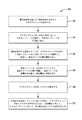
図7は例示的プロセスフロー700を示す。ブロック702において、プラズマチャンバが提供され、プラズマチャンバは、電気絶縁体を備える主要本体部分を含む。主要本体部分は、いくつかの例において、プラズマチャンバ壁の表面領域の大多数をカバーすることができる。ブロック704において、引き出しプレートが、プラズマチャンバの引き出し側面に沿って、提供される。引き出しプレートは、導電性にすることができ、異なる実施形態において、引き出し側面の全部又は一部にわたって延びることができる。ブロック706において、基板を保持する基板ステージを、プラズマチャンバの外側で、引き出しプレートの引き出しアパーチャに隣接して、配置し、基板ステージは接地電位にある。基板ステージは接地電位にまた維持される基板を保持することができる。ブロック708において、接地プレートは、引き出しアパーチャと基板ステージとの間に配置され、接地プレートは、導電材料を備え、接地電位に連結される。接地プレートは、引き出しアパーチャと共に、プラズマチャンバと基板との間の視線を提供する接地プレートアパーチャを含むことができる。接地プレートは、非対称の電極構成における接地電極として作動するように、引き出しプレートのターゲット距離内に配置することができる。ブロック710において、プラズマチャンバの中にプラズマを発生する。ブロック712において、RF電圧を引き出しプレートにおいて生成し、プラズマチャンバの中にプラズマが存在するときに、接地電位に対して、引き出しプレートにおいて、正の直流自己バイアス電圧を定める。
FIG. 7 shows an
本実施形態は、絶縁変圧器の必要なく、プラズマチャンバを高電圧に引き上げる必要もなく、コンパクトな処理装置において、イオンビームを基板へ送る機能を含む多数の優位性を提供する。さらに、様々な実施形態は、高価なパルス状の直流電源を業界標準のRFシステムに取り換えさせる。他の優位性は、従来のパルス状の直流処理装置に比べて、コンパクトなイオンビーム処理装置において、基板に十分な中性化を提供する機能を含む。 This embodiment provides a number of advantages, including the ability to send an ion beam to a substrate in a compact processing apparatus, without the need for an insulated transformer and without the need to raise the plasma chamber to a high voltage. In addition, various embodiments replace expensive pulsed DC power supplies with industry standard RF systems. Other advantages include the ability to provide sufficient neutralization of the substrate in a compact ion beam processing device as compared to conventional pulsed DC processing devices.
本発明は、本明細書に記載された特定の実施形態によって範囲を限定されるものではない。実際に、本明細書に記載された実施形態に加えて、本発明の他の様々な実施形態および変更は、前述の記載および添付図面から当業者には明らかであろう。したがって、このような他の実施形態および変更は、本発明の範囲内に含まれるものと意図している。さらに、本発明は、特定の環境における特定の目的のための特定の実装の文脈にて本明細書中で説明したけれども、当業者は、その有用性はそれらに限定されるものでなく、本発明は任意の数の環境における任意の数の目的のために有益に実装し得ることを認識するであろう。従って、以下に記載する特許請求の範囲は本明細書に記載された本発明の全範囲及び精神に鑑みて解釈しなければならない。 The present invention is not limited in scope by the particular embodiments described herein. Indeed, in addition to the embodiments described herein, various other embodiments and modifications of the invention will be apparent to those skilled in the art from the aforementioned description and accompanying drawings. Therefore, such other embodiments and modifications are intended to be included within the scope of the present invention. Moreover, although the present invention has been described herein in the context of a particular implementation for a particular purpose in a particular environment, those skilled in the art are not limited to those of use in the present invention. It will be appreciated that the invention can be beneficially implemented for any number of purposes in any number of environments. Therefore, the claims described below must be construed in light of the full scope and spirit of the invention described herein.
Claims (14)
該プラズマチャンバの引き出し側面に沿って配置され、導電性であり、引き出しアパーチャを有する、引き出しプレートと、
前記プラズマチャンバの外側に配置され、前記引き出しアパーチャに隣接し、接地電位にある、基板ステージと、
前記引き出しプレートに電気的に連結され、前記プラズマチャンバの中に前記プラズマが存在するときに、前記引き出しプレートにおいて、接地電位に対して正の直流自己バイアス電圧を定める、RF発生器と、を備え、
前記RF発生器は、前記引き出しプレートにおいて、2MHzから60MHzの周波数を有するRF電圧信号を発生する回路を備え、該RF電圧信号は、正の部分及び負の部分を有する波形を備え、電子は、前記負の部分の間に、前記引き出しアパーチャを通って引き出され、前記基板ステージへ向けられる、処理装置。 A plasma chamber, which houses the plasma and has a main body part with electrical insulation,
With a drawer plate located along the drawer side of the plasma chamber, which is conductive and has a drawer aperture,
A substrate stage located outside the plasma chamber, adjacent to the drawer aperture and at ground potential.
An RF generator that is electrically connected to the extraction plate and that, when the plasma is present in the plasma chamber, determines a positive DC self-bias voltage with respect to the ground potential in the extraction plate. ,
The RF generator comprises a circuit that generates an RF voltage signal having a frequency of 2 MHz to 60 MHz in the lead-out plate, the RF voltage signal has a waveform having a positive part and a negative part, and the electron is an electron. during the negative part, drawn through the extraction aperture, Ru directed to the substrate stage, processing apparatus.
前記処理装置は、さらに、
前記プラズマチャンバに隣接して配置される、RFアンテナと、
該RFアンテナに、直接、連結される、誘導結合xプラズマ(ICP)マッチングネットワークと、
該ICPマッチングネットワークに連結される、ICP RF発生器と、
前記バイアスRF発生器と前記引き出しプレートとの間に電気的に連結される、バイアスマッチングネットワークと、を備える、請求項1記載の処理装置。 The RF generator comprises a bias RF generator.
The processing device further
An RF antenna placed adjacent to the plasma chamber and
An inductively coupled x plasma (ICP) matching network that is directly connected to the RF antenna.
An ICP RF generator connected to the ICP matching network,
The processing apparatus according to claim 1, further comprising a bias matching network that is electrically connected between the bias RF generator and the drawer plate.
前記RF発生器、前記引き出しプレート、及び、前記プラズマチャンバに隣接するRFアンテナに連結される、デュアル出力マッチングネットワークを備え、
前記RF発生器は、前記プラズマチャンバの中で前記プラズマを発生し、前記引き出しプレートにおいて、RF電圧を発生する、請求項1記載の処理装置。 The processing device further
It comprises a dual output matching network connected to the RF generator, the drawer plate, and an RF antenna adjacent to the plasma chamber.
The processing apparatus according to claim 1, wherein the RF generator generates the plasma in the plasma chamber and generates an RF voltage in the drawing plate.
前記引き出しプレートと前記基板ステージとの間に配置され、導電材料を備え、接地電位に連結され、さらに、接地プレートアパーチャを備える、接地プレートを備え、
前記引き出しアパーチャ及び前記接地プレートアパーチャは、前記プラズマと前記基板ステージとの間の視線を提供する、請求項1記載の処理装置。 The processing device further
A grounding plate located between the drawer plate and the substrate stage, comprising a conductive material, connected to a grounding potential, and further comprising a grounding plate aperture.
The processing apparatus according to claim 1, wherein the drawer aperture and the ground plate aperture provide a line of sight between the plasma and the substrate stage.
前記処理装置は、さらに、
前記プラズマチャンバに隣接して配置される、RFアンテナと、
該RFアンテナに、直接、連結される、誘導結合xプラズマ(ICP)マッチングネットワークと、
該ICPマッチングネットワークに連結される、ICP RF発生器と、
前記バイアスRF発生器と前記引き出しプレートとの間に電気的に連結される、バイアスマッチングネットワークと、を備える、請求項4記載の処理装置。 The RF generator comprises a bias RF generator.
The processing device further
An RF antenna placed adjacent to the plasma chamber and
An inductively coupled x plasma (ICP) matching network that is directly connected to the RF antenna.
An ICP RF generator connected to the ICP matching network,
The processing apparatus according to claim 4, further comprising a bias matching network that is electrically connected between the bias RF generator and the drawer plate.
前記RF発生器、前記引き出しプレート、及び、前記プラズマチャンバに隣接するRFアンテナに連結される、デュアル出力マッチングネットワークを備え、
前記RF発生器は、前記プラズマチャンバの中で前記プラズマを発生し、前記引き出しプレートにおいて、RF電圧を発生する、請求項4記載の処理装置。 The processing device further
It comprises a dual output matching network connected to the RF generator, the drawer plate, and an RF antenna adjacent to the plasma chamber.
The processing apparatus according to claim 4, wherein the RF generator generates the plasma in the plasma chamber and generates an RF voltage in the drawing plate.
前記プラズマチャンバの中にプラズマを発生するステップと、
前記プラズマチャンバの引き出し側面に沿って引き出しプレートを提供するステップであって、該引き出しプレートは、導電性であり、引き出しアパーチャを有する、ステップと、
基板を保持する基板ステージを、前記プラズマチャンバの外側で、前記引き出しアパーチャに隣接して、配置するステップであって、前記基板ステージは接地電位にある、ステップと、
RF発生器により、RF電圧を前記引き出しプレートにおいて生成するステップと、を有し、
前記プラズマチャンバの中に前記プラズマが存在するときに、接地電位に対して、前記引き出しプレートにおいて、前記RF発生器により、正の直流自己バイアス電圧を定め、該正の直流自己バイアス電圧に比例するイオンエネルギーを有するイオンビームを、前記基板へ向け、
前記RF発生器は、前記引き出しプレートにおいて、2MHzから60MHzの周波数を有するRF電圧信号を発生する回路を備え、該RF電圧信号は、正の部分及び負の部分を有する波形を備え、電子は、前記負の部分の間に、前記引き出しアパーチャを通って引き出され、前記基板ステージへ向けられる、基板を処理する方法。 Steps to provide a plasma chamber with a main body portion with electrical insulation,
The step of generating plasma in the plasma chamber and
A step of providing a drawer plate along the drawer side of the plasma chamber, wherein the drawer plate is conductive and has a drawer aperture.
A step of arranging a substrate stage holding a substrate outside the plasma chamber, adjacent to the drawer aperture, wherein the substrate stage is at ground potential.
With a step of generating an RF voltage in the drawer plate by an RF generator,
When the plasma is present in the plasma chamber, a positive DC self-bias voltage is determined by the RF generator in the lead-out plate with respect to the ground potential and is proportional to the positive DC self-bias voltage. An ion beam having ion energy is directed toward the substrate,
The RF generator comprises a circuit that generates an RF voltage signal having a frequency of 2 MHz to 60 MHz in the lead-out plate, the RF voltage signal has a waveform having a positive part and a negative part, and the electron is an electron. during the negative part, drawn through the extraction aperture, Ru directed to the substrate stage, a method of processing a substrate.
前記接地プレートは、導電材料を備え、接地電位に連結され、前記接地プレートは、さらに、接地プレートアパーチャを備え、前記引き出しアパーチャ及び前記接地プレートアパーチャは、前記プラズマと前記基板ステージとの間の視線を提供する、請求項10記載の基板を処理する方法。 It further has a step of arranging the grounding plate between the drawer aperture and the substrate stage.
The ground plate comprises a conductive material and is connected to a ground potential, the ground plate further comprises a ground plate aperture, and the drawer aperture and the ground plate aperture are lines of sight between the plasma and the substrate stage. provides a method of processing a substrate according to claim 1 0, wherein.
前記第1の長軸に平行に並ぶ第2の長軸を有する第2の細長いアパーチャとして前記接地プレートアパーチャを提供するステップと、をさらに有し、
前記引き出しアパーチャは、前記第1の長軸に垂直な短軸に沿って第1の高さを備え、前記接地プレートアパーチャは、前記第1の高さより低い前記短軸に沿う第2の高さを備える、請求項11記載の基板を処理する方法。 A step of providing the drawer aperture as a first elongated aperture with a first major axis, and
It further comprises a step of providing the ground plate aperture as a second elongated aperture having a second major axis aligned parallel to the first major axis.
The drawer aperture has a first height along a minor axis perpendicular to the first major axis, and the ground plate aperture has a second height along the minor axis that is lower than the first height. the method comprises, for processing a substrate according to claim 1 1, wherein the.
該プラズマチャンバに電気的に連結され、前記プラズマチャンバの中にプラズマを発生する、第1のRF発生器と、
前記プラズマチャンバの引き出し側面に沿って配置され、導電性であり、引き出しアパーチャを有する、引き出しプレートと、
前記プラズマチャンバの外側に配置され、前記引き出しアパーチャに隣接し、接地電位にある、基板ステージと、
前記引き出しプレートと前記基板ステージとの間に配置され、導電材料を備え、接地電位に連結され、さらに、接地プレートアパーチャを備える、接地プレートと、
前記引き出しプレートに電気的に連結され、前記プラズマチャンバの中に前記プラズマが存在するときに、前記引き出しプレートにおいて、接地電位に対して正の直流自己バイアス電圧を定める、第2のRF発生器と、を備え、
前記第2のRF発生器は、前記引き出しプレートにおいて、2MHzから60MHzの周波数を有するRF電圧信号を発生する回路を備え、該RF電圧信号は、正の部分及び負の部分を有する波形を備え、電子は、前記負の部分の間に、前記引き出しアパーチャを通って引き出され、前記基板ステージへ向けられる処理装置。
With a plasma chamber, which has a main body part with electrical insulation,
A first RF generator that is electrically connected to the plasma chamber and generates plasma in the plasma chamber.
With a drawer plate located along the drawer side of the plasma chamber, which is conductive and has a drawer aperture.
A substrate stage located outside the plasma chamber, adjacent to the drawer aperture and at ground potential.
A grounding plate located between the drawer plate and the substrate stage, comprising a conductive material, connected to a grounding potential, and further comprising a grounding plate aperture.
With a second RF generator that is electrically connected to the extraction plate and that, when the plasma is present in the plasma chamber, determines a positive DC self-bias voltage with respect to the ground potential in the extraction plate. , With
The second RF generator comprises a circuit in the lead-out plate that generates an RF voltage signal having a frequency of 2 MHz to 60 MHz, the RF voltage signal having a waveform having a positive portion and a negative portion. electrons, during the negative portion is drawn through said pull-out aperture, it said that directed to the substrate stage processing apparatus.
Applications Claiming Priority (3)
| Application Number | Priority Date | Filing Date | Title |
|---|---|---|---|
| US15/133,261 US10224181B2 (en) | 2016-04-20 | 2016-04-20 | Radio frequency extraction system for charge neutralized ion beam |
| US15/133,261 | 2016-04-20 | ||
| PCT/US2017/028372 WO2017184736A1 (en) | 2016-04-20 | 2017-04-19 | Radio frequency extraction system for charge neutralized ion beam |
Publications (3)
| Publication Number | Publication Date |
|---|---|
| JP2019519064A JP2019519064A (en) | 2019-07-04 |
| JP2019519064A5 JP2019519064A5 (en) | 2020-05-28 |
| JP6944949B2 true JP6944949B2 (en) | 2021-10-06 |
Family
ID=60089727
Family Applications (1)
| Application Number | Title | Priority Date | Filing Date |
|---|---|---|---|
| JP2018553427A Active JP6944949B2 (en) | 2016-04-20 | 2017-04-19 | Radio frequency extraction system for charge-neutralized ion beams |
Country Status (6)
| Country | Link |
|---|---|
| US (1) | US10224181B2 (en) |
| JP (1) | JP6944949B2 (en) |
| KR (1) | KR102268345B1 (en) |
| CN (1) | CN109417012B (en) |
| TW (1) | TWI734755B (en) |
| WO (1) | WO2017184736A1 (en) |
Families Citing this family (5)
| Publication number | Priority date | Publication date | Assignee | Title |
|---|---|---|---|---|
| WO2019182191A1 (en) | 2018-03-21 | 2019-09-26 | 경북대학교 산학협력단 | Pharmaceutical composition for prevention or treatment of neurodegenerative disease and comprising cox2-acetylating agent as active ingredient |
| US11056319B2 (en) * | 2019-07-29 | 2021-07-06 | Applied Materials, Inc. | Apparatus and system having extraction assembly for wide angle ion beam |
| WO2021054778A1 (en) | 2019-09-20 | 2021-03-25 | 경북대학교 산학협력단 | Antibody for detecting acetylation of cox2 protein, and uses thereof |
| CN113539773A (en) * | 2020-04-16 | 2021-10-22 | 新动力等离子体株式会社 | High frequency generator with dual output and driving method thereof |
| US11495430B2 (en) | 2020-07-15 | 2022-11-08 | Applied Materials, Inc. | Tunable extraction assembly for wide angle ion beam |
Family Cites Families (14)
| Publication number | Priority date | Publication date | Assignee | Title |
|---|---|---|---|---|
| US6478924B1 (en) * | 2000-03-07 | 2002-11-12 | Applied Materials, Inc. | Plasma chamber support having dual electrodes |
| JP2007242368A (en) * | 2006-03-07 | 2007-09-20 | Shincron:Kk | Neutralizer, and film forming device equipped with this |
| US7498592B2 (en) | 2006-06-28 | 2009-03-03 | Wisconsin Alumni Research Foundation | Non-ambipolar radio-frequency plasma electron source and systems and methods for generating electron beams |
| US20080132046A1 (en) * | 2006-12-04 | 2008-06-05 | Varian Semiconductor Equipment Associates, Inc. | Plasma Doping With Electronically Controllable Implant Angle |
| US20090084987A1 (en) * | 2007-09-28 | 2009-04-02 | Varian Semiconductor Equipment Associates, Inc. | Charge neutralization in a plasma processing apparatus |
| JP2011514441A (en) * | 2008-01-30 | 2011-05-06 | アプライド マテリアルズ インコーポレイテッド | System and method for preionization of a surface wave initiated plasma discharge source |
| US20120104274A1 (en) * | 2009-07-16 | 2012-05-03 | Canon Anelva Corporation | Ion beam generating apparatus, substrate processing apparatus and method of manufacturing electronic device |
| US20130098871A1 (en) | 2011-10-19 | 2013-04-25 | Fei Company | Internal Split Faraday Shield for an Inductively Coupled Plasma Source |
| JP5495138B2 (en) * | 2011-10-31 | 2014-05-21 | 日新イオン機器株式会社 | Ion source |
| US8907300B2 (en) * | 2013-03-14 | 2014-12-09 | Varian Semiconductor Equipment Associates, Inc. | System and method for plasma control using boundary electrode |
| US9711316B2 (en) | 2013-10-10 | 2017-07-18 | Varian Semiconductor Equipment Associates, Inc. | Method of cleaning an extraction electrode assembly using pulsed biasing |
| US9269542B2 (en) * | 2013-11-01 | 2016-02-23 | Varian Semiconductor Equipment Associates, Inc. | Plasma cathode charged particle lithography system |
| FR3020235B1 (en) | 2014-04-17 | 2016-05-27 | Ecole Polytech | DEVICE FOR FORMING A NEAR-NEUTRAL BEAM OF PARTICLES OF OPPOSED LOADS. |
| US9230773B1 (en) | 2014-10-16 | 2016-01-05 | Varian Semiconductor Equipment Associates, Inc. | Ion beam uniformity control |
-
2016
- 2016-04-20 US US15/133,261 patent/US10224181B2/en active Active
-
2017
- 2017-03-21 TW TW106109286A patent/TWI734755B/en active
- 2017-04-19 JP JP2018553427A patent/JP6944949B2/en active Active
- 2017-04-19 KR KR1020187033334A patent/KR102268345B1/en active IP Right Grant
- 2017-04-19 WO PCT/US2017/028372 patent/WO2017184736A1/en active Application Filing
- 2017-04-19 CN CN201780024188.5A patent/CN109417012B/en active Active
Also Published As
| Publication number | Publication date |
|---|---|
| WO2017184736A1 (en) | 2017-10-26 |
| KR102268345B1 (en) | 2021-06-24 |
| CN109417012B (en) | 2021-07-09 |
| US10224181B2 (en) | 2019-03-05 |
| TW201802860A (en) | 2018-01-16 |
| KR20180127656A (en) | 2018-11-29 |
| JP2019519064A (en) | 2019-07-04 |
| US20170309453A1 (en) | 2017-10-26 |
| CN109417012A (en) | 2019-03-01 |
| TWI734755B (en) | 2021-08-01 |
Similar Documents
| Publication | Publication Date | Title |
|---|---|---|
| JP6944949B2 (en) | Radio frequency extraction system for charge-neutralized ion beams | |
| JP3912993B2 (en) | Neutral particle beam processing equipment | |
| KR20210038938A (en) | Method and apparatus for plasma processing | |
| US11462389B2 (en) | Pulsed-voltage hardware assembly for use in a plasma processing system | |
| JP2008294440A (en) | Plasma ion implantation system | |
| TW201306085A (en) | Projected plasma source | |
| JP7330361B2 (en) | Devices and systems with extraction assemblies for wide-angle ion beams | |
| US20210287907A1 (en) | Methods and apparatus for processing a substrate | |
| CN116018665A (en) | Time domain multiplexing of voltage pulses | |
| JP6114262B2 (en) | Ion implanter in plasma immersion mode for low pressure process | |
| KR20190046194A (en) | Plasma processing apparatus and method of fabricating semiconductor device using the same | |
| KR20190104093A (en) | An antenna structure for a high density linear ICP source | |
| US11495430B2 (en) | Tunable extraction assembly for wide angle ion beam | |
| KR20230026484A (en) | How to Improve Etch Selectivity Using Pulsed Plasma | |
| KR100633167B1 (en) | Apparatus for treating substrate and method of treating substrate | |
| KR20210027221A (en) | Plasma processing apparatus and processing method | |
| TW201401326A (en) | A machine for implanting ions in plasma immersion mode for a low-pressure method |
Legal Events
| Date | Code | Title | Description |
|---|---|---|---|
| A521 | Request for written amendment filed |
Free format text: JAPANESE INTERMEDIATE CODE: A523 Effective date: 20200416 |
|
| A621 | Written request for application examination |
Free format text: JAPANESE INTERMEDIATE CODE: A621 Effective date: 20200416 |
|
| A131 | Notification of reasons for refusal |
Free format text: JAPANESE INTERMEDIATE CODE: A131 Effective date: 20210216 |
|
| A521 | Request for written amendment filed |
Free format text: JAPANESE INTERMEDIATE CODE: A523 Effective date: 20210511 |
|
| TRDD | Decision of grant or rejection written | ||
| A01 | Written decision to grant a patent or to grant a registration (utility model) |
Free format text: JAPANESE INTERMEDIATE CODE: A01 Effective date: 20210824 |
|
| A61 | First payment of annual fees (during grant procedure) |
Free format text: JAPANESE INTERMEDIATE CODE: A61 Effective date: 20210913 |
|
| R150 | Certificate of patent or registration of utility model |
Ref document number: 6944949 Country of ref document: JP Free format text: JAPANESE INTERMEDIATE CODE: R150 |