JP6932552B2 - Mask blank, transfer mask manufacturing method and semiconductor device manufacturing method - Google Patents
Mask blank, transfer mask manufacturing method and semiconductor device manufacturing method Download PDFInfo
- Publication number
- JP6932552B2 JP6932552B2 JP2017107767A JP2017107767A JP6932552B2 JP 6932552 B2 JP6932552 B2 JP 6932552B2 JP 2017107767 A JP2017107767 A JP 2017107767A JP 2017107767 A JP2017107767 A JP 2017107767A JP 6932552 B2 JP6932552 B2 JP 6932552B2
- Authority
- JP
- Japan
- Prior art keywords
- light
- shielding film
- mask
- film
- translucent substrate
- Prior art date
- Legal status (The legal status is an assumption and is not a legal conclusion. Google has not performed a legal analysis and makes no representation as to the accuracy of the status listed.)
- Active
Links
Images


Classifications
-
- G—PHYSICS
- G03—PHOTOGRAPHY; CINEMATOGRAPHY; ANALOGOUS TECHNIQUES USING WAVES OTHER THAN OPTICAL WAVES; ELECTROGRAPHY; HOLOGRAPHY
- G03F—PHOTOMECHANICAL PRODUCTION OF TEXTURED OR PATTERNED SURFACES, e.g. FOR PRINTING, FOR PROCESSING OF SEMICONDUCTOR DEVICES; MATERIALS THEREFOR; ORIGINALS THEREFOR; APPARATUS SPECIALLY ADAPTED THEREFOR
- G03F1/00—Originals for photomechanical production of textured or patterned surfaces, e.g., masks, photo-masks, reticles; Mask blanks or pellicles therefor; Containers specially adapted therefor; Preparation thereof
- G03F1/54—Absorbers, e.g. of opaque materials
-
- G—PHYSICS
- G03—PHOTOGRAPHY; CINEMATOGRAPHY; ANALOGOUS TECHNIQUES USING WAVES OTHER THAN OPTICAL WAVES; ELECTROGRAPHY; HOLOGRAPHY
- G03F—PHOTOMECHANICAL PRODUCTION OF TEXTURED OR PATTERNED SURFACES, e.g. FOR PRINTING, FOR PROCESSING OF SEMICONDUCTOR DEVICES; MATERIALS THEREFOR; ORIGINALS THEREFOR; APPARATUS SPECIALLY ADAPTED THEREFOR
- G03F1/00—Originals for photomechanical production of textured or patterned surfaces, e.g., masks, photo-masks, reticles; Mask blanks or pellicles therefor; Containers specially adapted therefor; Preparation thereof
- G03F1/50—Mask blanks not covered by G03F1/20 - G03F1/34; Preparation thereof
-
- G—PHYSICS
- G03—PHOTOGRAPHY; CINEMATOGRAPHY; ANALOGOUS TECHNIQUES USING WAVES OTHER THAN OPTICAL WAVES; ELECTROGRAPHY; HOLOGRAPHY
- G03F—PHOTOMECHANICAL PRODUCTION OF TEXTURED OR PATTERNED SURFACES, e.g. FOR PRINTING, FOR PROCESSING OF SEMICONDUCTOR DEVICES; MATERIALS THEREFOR; ORIGINALS THEREFOR; APPARATUS SPECIALLY ADAPTED THEREFOR
- G03F7/00—Photomechanical, e.g. photolithographic, production of textured or patterned surfaces, e.g. printing surfaces; Materials therefor, e.g. comprising photoresists; Apparatus specially adapted therefor
- G03F7/20—Exposure; Apparatus therefor
- G03F7/2002—Exposure; Apparatus therefor with visible light or UV light, through an original having an opaque pattern on a transparent support, e.g. film printing, projection printing; by reflection of visible or UV light from an original such as a printed image
- G03F7/2004—Exposure; Apparatus therefor with visible light or UV light, through an original having an opaque pattern on a transparent support, e.g. film printing, projection printing; by reflection of visible or UV light from an original such as a printed image characterised by the use of a particular light source, e.g. fluorescent lamps or deep UV light
- G03F7/2006—Exposure; Apparatus therefor with visible light or UV light, through an original having an opaque pattern on a transparent support, e.g. film printing, projection printing; by reflection of visible or UV light from an original such as a printed image characterised by the use of a particular light source, e.g. fluorescent lamps or deep UV light using coherent light; using polarised light
-
- H—ELECTRICITY
- H01—ELECTRIC ELEMENTS
- H01L—SEMICONDUCTOR DEVICES NOT COVERED BY CLASS H10
- H01L21/00—Processes or apparatus adapted for the manufacture or treatment of semiconductor or solid state devices or of parts thereof
- H01L21/02—Manufacture or treatment of semiconductor devices or of parts thereof
- H01L21/027—Making masks on semiconductor bodies for further photolithographic processing not provided for in group H01L21/18 or H01L21/34
- H01L21/0271—Making masks on semiconductor bodies for further photolithographic processing not provided for in group H01L21/18 or H01L21/34 comprising organic layers
- H01L21/0273—Making masks on semiconductor bodies for further photolithographic processing not provided for in group H01L21/18 or H01L21/34 comprising organic layers characterised by the treatment of photoresist layers
- H01L21/0274—Photolithographic processes
Description
本発明は、マスクブランク、そのマスクブランクを用いて製造された転写用マスクの製造方法に関するものである。また、本発明は、上記の転写用マスクを用いた半導体デバイスの製造方法に関するものである。 The present invention relates to a mask blank and a method for manufacturing a transfer mask manufactured by using the mask blank. The present invention also relates to a method for manufacturing a semiconductor device using the above-mentioned transfer mask.
半導体デバイスの製造工程では、フォトリソグラフィー法を用いて微細パターンの形成が行われている。また、この微細パターンの形成には通常何枚もの転写用マスクが使用される。半導体デバイスのパターンを微細化するに当たっては、転写用マスクに形成されるマスクパターンの微細化に加え、フォトリソグラフィーで使用される露光光源の波長の短波長化が必要となる。近年、半導体装置を製造する際の露光光源にArFエキシマレーザー(波長193nm)が適用されることが増えてきている。 In the manufacturing process of a semiconductor device, a fine pattern is formed by using a photolithography method. In addition, a number of transfer masks are usually used to form this fine pattern. In order to miniaturize the pattern of a semiconductor device, it is necessary to shorten the wavelength of the exposure light source used in photolithography in addition to miniaturizing the mask pattern formed on the transfer mask. In recent years, an ArF excimer laser (wavelength 193 nm) has been increasingly applied as an exposure light source when manufacturing a semiconductor device.
転写用マスクには、様々な種類があるが、その中でもバイナリマスクとハーフトーン型位相シフトマスクが広く用いられている。従来のバイナリマスクは、透光性基板上にクロム系材料からなる遮光膜パターンを備えたものが一般的であったが、近年、遷移金属シリサイド系材料で遮光膜が形成されたバイナリマスクが用いられ始めている。しかし、特許文献1に開示されている通り、遷移金属シリサイド系材料の遮光膜は、ArFエキシマレーザーの露光光(ArF露光光)に対する耐性(いわゆるArF耐光性)が低いということが近年判明している。特許文献1では、遷移金属シリサイドに炭素または水素を含有させた材料を遮光膜に適用することによってArF耐光性を高めることが行われている。
There are various types of transfer masks, and among them, a binary mask and a halftone type phase shift mask are widely used. Conventional binary masks generally have a light-shielding film pattern made of a chrome-based material on a translucent substrate, but in recent years, binary masks in which a light-shielding film is formed of a transition metal silicide-based material have been used. Is beginning to be. However, as disclosed in
一方、特許文献2では、SiNxの位相シフト膜を備える位相シフトマスクが開示されている。特許文献3では、SiNxの位相シフト膜は高いArF耐光性を有することが確認されたことが記されている。他方、特許文献4には、遮光膜の黒欠陥部分に対して、二フッ化キセノン(XeF2)ガスを供給しつつ、その部分に電子線を照射することで黒欠陥部分をエッチングして除去する欠陥修正技術(以下、このような電子線等の荷電粒子を照射して行う欠陥修正を単にEB欠陥修正という。)が開示されている。
On the other hand,
特許文献2や特許文献3に開示されているような遷移金属を含有しないケイ素と窒素を含有する材料(以下、SiN系材料という。)からなる位相シフト膜は、ArF耐光性が高いことが既に知られている。本発明者らは、バイナリマスクの遮光膜にこのSiN系材料を適用することを試みたところ、遮光膜のArF耐光性を高めることができた。しかし、SiN系材料の遮光膜のパターンに見つかった黒欠陥部分に対してEB欠陥修正を行ったところ、2つの大きな問題が生じることが判明した。
A phase shift film made of a material containing silicon and nitrogen (hereinafter referred to as SiN-based material) that does not contain a transition metal as disclosed in
1つの大きな問題は、EB欠陥修正を行って遮光膜の黒欠陥部分を除去したときに、黒欠陥が存在していた領域の透光性基板の表面が大きく荒れてしまう(表面粗さが大幅に悪化する)ことであった。EB欠陥修正後のバイナリマスクにおける表面が荒れた領域は、ArF露光光を透過させる透光部になる領域である。透光部の基板の表面粗さが大幅に悪化するとArF露光光の透過率の低下や乱反射などが生じやすく、そのようなバイナリマスクは露光装置のマスクステージに設置して露光転写に使用するときに転写精度の大幅な低下を招く。 One major problem is that when the black defect portion of the light-shielding film is removed by correcting the EB defect, the surface of the translucent substrate in the region where the black defect existed becomes greatly roughened (the surface roughness is large). It was to get worse). The rough surface region of the binary mask after the EB defect correction is a region that becomes a translucent portion that transmits ArF exposure light. When the surface roughness of the substrate of the translucent part is significantly deteriorated, the transmittance of ArF exposure light is likely to decrease and diffuse reflection is likely to occur. When such a binary mask is installed on the mask stage of an exposure apparatus and used for exposure transfer. This causes a significant decrease in transfer accuracy.
もう1つの大きな問題は、EB欠陥修正を行って遮光膜の黒欠陥部分を除去するときに、黒欠陥部分の周囲に存在する遮光膜パターンが側壁からエッチングされてしまうことであった(この現象を自発性エッチングという。)。自発性エッチングが発生した場合、遮光膜パターンがEB欠陥修正前の幅よりも大幅に細くなってしまうことが生じる。EB欠陥修正前の段階で幅が細い遮光膜パターンの場合、パターンの脱落や消失が発生する恐れもある。このような自発性エッチングが生じやすい遮光膜のパターンを備えるバイナリマスクは、露光装置のマスクステージに設置して露光転写に使用するときに、転写精度の大幅な低下を招く。 Another major problem was that when the black defect portion of the light-shielding film was removed by performing EB defect correction, the light-shielding film pattern existing around the black defect portion was etched from the side wall (this phenomenon). Is called spontaneous etching.) When spontaneous etching occurs, the light-shielding film pattern may become significantly thinner than the width before EB defect correction. In the case of a light-shielding film pattern having a narrow width before the EB defect is corrected, the pattern may fall off or disappear. A binary mask provided with a light-shielding film pattern in which spontaneous etching is likely to occur causes a significant decrease in transfer accuracy when it is installed on a mask stage of an exposure apparatus and used for exposure transfer.
そこで、本発明は、従来の課題を解決するためになされたものであり、SiN系材料で形成された遮光膜の黒欠陥部分に対してEB欠陥修正を行った場合に、透光性基板の表面荒れの発生を抑制でき、かつ遮光膜のパターンに自発性エッチングが発生することを抑制できるマスクブランクを提供することを目的とする。また、本発明は、このマスクブランクを用いた転写用マスクの製造方法を提供することを目的とする。さらに、本発明は、この転写用マスクを用いた半導体デバイスの製造方法を提供することを目的とする。 Therefore, the present invention has been made to solve the conventional problems, and when EB defects are corrected for the black defect portion of the light-shielding film formed of SiN-based material, the translucent substrate is used. It is an object of the present invention to provide a mask blank capable of suppressing the occurrence of surface roughness and suppressing the occurrence of spontaneous etching in the pattern of the light-shielding film. Another object of the present invention is to provide a method for producing a transfer mask using this mask blank. Furthermore, an object of the present invention is to provide a method for manufacturing a semiconductor device using this transfer mask.
前記の課題を達成するため、本発明は以下の構成を有する。 In order to achieve the above object, the present invention has the following configuration.
(構成1)
透光性基板上に、転写パターンを形成するための遮光膜を備えたマスクブランクであって、
前記遮光膜は、ケイ素と窒素とからなる材料、または半金属元素および非金属元素から選ばれる1以上の元素とケイ素と窒素とからなる材料で形成され、
前記遮光膜の前記透光性基板との界面の近傍領域と前記遮光膜の前記透光性基板とは反対側の表層領域を除いた内部領域におけるSi3N4結合の存在数を、Si3N4結合、SiaNb結合(ただし、b/[a+b]<4/7)およびSi−Si結合の合計存在数で除した比率が0.04以下であり、
前記遮光膜の前記内部領域におけるSiaNb結合の存在数を、Si3N4結合、SiaNb結合およびSi−Si結合の合計存在数で除した比率が0.1以上である
ことを特徴とするマスクブランク。
(Structure 1)
A mask blank provided with a light-shielding film for forming a transfer pattern on a translucent substrate.
The light-shielding film is formed of a material composed of silicon and nitrogen, or a material composed of one or more elements selected from metalloid elements and non-metal elements, and silicon and nitrogen.
The number of Si 3 N 4 bonds present in the internal region excluding the region near the interface of the light-shielding film with the translucent substrate and the surface layer region on the side opposite to the translucent substrate of the light-shielding film is determined by Si 3. The ratio divided by the total number of N 4 bonds, Si a N b bonds (however, b / [a + b] <4/7) and Si-Si bonds is 0.04 or less.
The ratio of the number of Si a N b bonds present in the internal region of the light-shielding film divided by the total number of Si 3 N 4 bonds, Si a N b bonds and Si-Si bonds is 0.1 or more. A mask blank characterized by.
(構成2)
前記遮光膜の前記表層領域を除いた領域は、酸素含有量が10原子%以下であることを特徴とする構成1記載のマスクブランク。
(Structure 2)
The mask blank according to
(構成3)
前記表層領域は、前記遮光膜における前記透光性基板とは反対側の表面から前記透光性基板側に向かって5nmの深さまでの範囲にわたる領域であることを特徴とする構成1または2に記載のマスクブランク。
(Structure 3)
The
(構成4)
前記近傍領域は、前記透光性基板との界面から前記表層領域側に向かって5nmの深さまでの範囲にわたる領域であることを特徴とする構成1から3のいずれかに記載のマスクブランク。
(Structure 4)
The mask blank according to any one of
(構成5)
前記遮光膜は、ケイ素、窒素および非金属元素からなる材料で形成されていることを特徴とする構成1から4のいずれかに記載のマスクブランク。
(Structure 5)
The mask blank according to any one of
(構成6)
前記表層領域は、前記遮光膜の表層領域を除いた領域よりも酸素含有量が多いことを特徴とする構成1から5のいずれかに記載のマスクブランク。
(Structure 6)
The mask blank according to any one of
(構成7)
前記遮光膜は、ArFエキシマレーザーの露光光に対する光学濃度が2.5以上であることを特徴とする構成1から6のいずれかに記載のマスクブランク。
(Structure 7)
The mask blank according to any one of
(構成8)
前記遮光膜は、前記透光性基板の主表面に接して設けられていることを特徴とする構成1から7のいずれかに記載のマスクブランク。
(Structure 8)
The mask blank according to any one of
(構成9)
構成1から8のいずれかに記載のマスクブランクを用いた転写用マスクの製造方法であって、ドライエッチングにより前記遮光膜に転写パターンを形成する工程を備えることを特徴とする転写用マスクの製造方法。
(Structure 9)
A method for manufacturing a transfer mask using the mask blank according to any one of
(構成10)
構成9記載の転写用マスクの製造方法により製造された転写用マスクを用い、半導体基板上のレジスト膜に転写パターンを露光転写する工程を備えることを特徴とする半導体デバイスの製造方法。
(Structure 10)
A method for manufacturing a semiconductor device, which comprises a step of exposing and transferring a transfer pattern to a resist film on a semiconductor substrate using the transfer mask manufactured by the method for manufacturing a transfer mask according to the configuration 9.
本発明のマスクブランクは、SiN系材料で形成された遮光膜パターンの黒欠陥部分に対してEB欠陥修正を行った場合に、透光性基板の表面荒れの発生を抑制でき、かつ遮光膜パターンに自発性エッチングが発生することを抑制できる。 The mask blank of the present invention can suppress the occurrence of surface roughness of the translucent substrate when the black defect portion of the light-shielding film pattern made of SiN-based material is corrected for EB defects, and the light-shielding film pattern. It is possible to suppress the occurrence of spontaneous etching.
本発明の転写用マスクの製造方法は、その転写用マスクの製造途上で遮光膜パターンの黒欠陥部分に対してEB欠陥修正を行った場合においても、透光性基板の表面荒れの発生が抑制でき、かつ黒欠陥部分の近傍の遮光膜パターンに自発性エッチングが発生することを抑制できる。 The method for manufacturing a transfer mask of the present invention suppresses the occurrence of surface roughness of a translucent substrate even when EB defects are corrected for a black defect portion of a light-shielding film pattern during the manufacture of the transfer mask. It is possible to suppress the occurrence of spontaneous etching in the light-shielding film pattern in the vicinity of the black defect portion.
このため、本発明の転写用マスクの製造方法で製造された転写用マスクは転写精度の高い転写用マスクとなる。 Therefore, the transfer mask produced by the method for producing the transfer mask of the present invention is a transfer mask with high transfer accuracy.
先ず、本発明の完成に至った経緯を述べる。 First, the background to the completion of the present invention will be described.
本発明者らは、SiN系材料で形成された遮光膜の黒欠陥部分に対してEB欠陥修正を行った場合に、透光性基板の表面荒れの発生が抑制され、かつ遮光膜のパターンに自発性エッチングが発生することが抑制された遮光膜の構成について鋭意研究を行った。まず、SiN系材料で形成された位相シフト膜のパターンに対してEB欠陥修正を行ったところ、修正レートが大幅に遅いという問題はあったが、自発性エッチングに係る実質的な問題は生じなかった。 When the black defect portion of the light-shielding film made of SiN-based material is corrected for EB defects, the present inventors suppress the occurrence of surface roughness of the translucent substrate and form the pattern of the light-shielding film. We conducted intensive research on the composition of the light-shielding film in which spontaneous etching was suppressed. First, when EB defect correction was performed on the pattern of the phase shift film formed of SiN-based material, there was a problem that the correction rate was significantly slow, but there was no substantial problem related to spontaneous etching. rice field.
EB欠陥修正で用いられるXeF2ガスは、ケイ素系材料に対して等方性エッチングを行うときの非励起状態のエッチングガスとして知られている。そのエッチングは、ケイ素系材料への非励起状態のXeF2ガスの表面吸着、XeとFに分離、ケイ素の高次フッ化物の生成、揮発というプロセスで行われる。ケイ素系材料の薄膜パターンに対するEB欠陥修正では、薄膜パターンの黒欠陥部分に対してXeF2ガス等の非励起状態のフッ素系ガスを供給し、黒欠陥部分の表面にそのフッ素系ガスを吸着させてから、黒欠陥部分に対して電子線を照射する。これにより、黒欠陥部分のケイ素は励起してフッ素との結合が促進され、電子線を照射しない場合よりも大幅に速くケイ素の高次フッ化物となって揮発する。黒欠陥部分の周囲の薄膜パターンにフッ素系ガスが吸着しないようにすることは困難であるため、EB欠陥修正時に黒欠陥部分の周囲の薄膜パターンもエッチングはされる。窒素と結合しているケイ素をエッチングする場合、XeF2ガスのフッ素がケイ素と結合してケイ素の高次フッ化物を生成するには、ケイ素と窒素の結合を断ち切る必要がある。電子線が照射された黒欠陥部分は、ケイ素が励起されるため、窒素との結合を断ち切ってフッ素と結合して揮発しやすくなる。一方、他の元素と未結合のケイ素は、フッ素と結合しやすい状態といえる。このため、他の元素と未結合のケイ素は、電子線の照射を受けず励起していない状態のものや、黒欠陥部分の周辺の遮光膜パターンであって電子線の照射の影響をわずかに受けた程度のものでも、フッ素と結合して揮発しやすい傾向がある。これが自発性エッチングの発生メカニズムと推測される。 The XeF 2 gas used for EB defect correction is known as a non-excited etching gas when isotropic etching is performed on a silicon-based material. The etching is performed by a process of surface adsorption of unexcited XeF 2 gas to a silicon-based material, separation into Xe and F, formation of higher-order fluoride of silicon, and volatilization. In EB defect correction for a thin film pattern of a silicon-based material, a non-excited fluorine-based gas such as XeF 2 gas is supplied to the black defect portion of the thin film pattern, and the fluorine-based gas is adsorbed on the surface of the black defect portion. Then, the black defect portion is irradiated with an electron beam. As a result, the silicon in the black defect portion is excited to promote the bond with fluorine, and becomes a higher-order fluoride of silicon and volatilizes much faster than in the case where the electron beam is not irradiated. Since it is difficult to prevent the fluorine-based gas from being adsorbed on the thin film pattern around the black defect portion, the thin film pattern around the black defect portion is also etched when the EB defect is corrected. When etching silicon that is bonded to nitrogen, it is necessary to break the bond between silicon and nitrogen in order for the fluorine in the XeF 2 gas to combine with silicon to form a higher-order fluoride of silicon. Since silicon is excited in the black defect portion irradiated with the electron beam, it breaks the bond with nitrogen and binds with fluorine to easily volatilize. On the other hand, silicon unbonded to other elements can be said to be in a state of being easily bonded to fluorine. For this reason, silicon that is unbonded to other elements is in a state where it is not excited without being irradiated by an electron beam, or it is a light-shielding film pattern around a black defect portion and is slightly affected by electron beam irradiation. Even if it is received, it tends to combine with fluorine and easily volatilize. This is presumed to be the mechanism of spontaneous etching.
ケイ素膜は、ArF露光光に対する屈折率nが大幅に小さく、消衰係数kが大きいため、位相シフト膜の材料には適さない。位相シフト膜の材料には、SiN系材料のうち、窒素を多く含有させて屈折率nを大きくし、消衰係数kを小さくしたSiN系材料が適している。このようなSiN系材料で形成された位相シフト膜は、膜中のケイ素が窒素と結合している比率が高く、他の元素と未結合のケイ素の比率は大幅に低いといえる。このため、このようなSiN系材料で形成された位相シフト膜は、EB欠陥修正時に自発性エッチングの問題が実質的に生じなかったと考えられる。一方、バイナリマスクの遮光膜は、ArF露光光に対する高い遮光性能、すなわち所定以上の光学濃度(OD:Optical Density)を有しつつ、厚さが薄いことが求められる。このため、遮光膜の材料は消衰係数kが大きい材料が求められる。これらの事情から、遮光膜に用いられるSiN系材料は、位相シフト膜に用いられるSiN系材料に比べて窒素含有量が大幅に少ない。そして、SiN系材料の遮光膜は、膜中のケイ素が窒素と結合している比率が低く、他の元素と未結合のケイ素の比率は高いといえる。このため、SiN系材料の遮光膜は、EB欠陥修正時に自発性エッチングの問題が生じやすくなっていると考えられる。 The silicon film is not suitable as a material for a phase shift film because it has a significantly small refractive index n with respect to ArF exposure light and a large extinction coefficient k. Among the SiN-based materials, the SiN-based material which contains a large amount of nitrogen to increase the refractive index n and decrease the extinction coefficient k is suitable as the material of the phase shift film. In a phase shift film formed of such a SiN-based material, it can be said that the ratio of silicon bonded to nitrogen in the film is high, and the ratio of silicon unbonded to other elements is significantly low. Therefore, it is considered that the phase shift film formed of such a SiN-based material does not substantially cause the problem of spontaneous etching when the EB defect is corrected. On the other hand, the light-shielding film of the binary mask is required to have high light-shielding performance against ArF exposure light, that is, to have an optical density (OD: Optical Density) equal to or higher than a predetermined value, and to have a thin thickness. Therefore, the material of the light-shielding film is required to have a large extinction coefficient k. For these reasons, the SiN-based material used for the light-shielding film has a significantly lower nitrogen content than the SiN-based material used for the phase shift film. It can be said that the light-shielding film of the SiN-based material has a low ratio of silicon bonded to nitrogen in the film and a high ratio of silicon unbonded to other elements. Therefore, it is considered that the light-shielding film made of SiN-based material tends to cause a problem of spontaneous etching when correcting EB defects.
次に、本発明者らは、遮光膜を形成するSiN系材料の窒素含有量を増やすことを検討した。位相シフト膜のSiN系材料のように窒素含有量を大幅に増やすと、消衰係数kが大幅に小さくなり、遮光膜の厚さが大幅に厚くなる必要が生じ、EB欠陥修正時の修正レートが低下する。これらのことを考慮し、窒素含有量をある程度増やしたSiN系材料の遮光膜を透光性基板上に形成し、EB欠陥修正を試みた。その結果、その遮光膜は、黒欠陥部分の修正レートが十分に大きく、かつ自発性エッチングの発生を抑制することができていたが、修正後の透光性基板の表面に顕著な荒れが発生していた。遮光膜の黒欠陥部分の修正レートが十分に大きいということは、透光性基板との間でのエッチング選択性が十分に高くなっており、透光性基板の表面を顕著に荒らすようなことは生じないはずであった。 Next, the present inventors examined increasing the nitrogen content of the SiN-based material forming the light-shielding film. When the nitrogen content is significantly increased as in the SiN-based material of the phase shift film, the extinction coefficient k becomes significantly smaller, and the thickness of the light-shielding film needs to be significantly increased. Decreases. In consideration of these facts, a light-shielding film of a SiN-based material having a certain amount of nitrogen content was formed on the translucent substrate, and an attempt was made to correct EB defects. As a result, the light-shielding film had a sufficiently high correction rate for black defects and was able to suppress the occurrence of spontaneous etching, but the surface of the light-transmitting substrate after correction was significantly roughened. Was. The fact that the correction rate of the black defect portion of the light-shielding film is sufficiently high means that the etching selectivity with and from the translucent substrate is sufficiently high, and the surface of the translucent substrate is significantly roughened. Should not have occurred.
本発明者らは、さらに鋭意研究を行った結果、遮光膜を形成するSiN系材料中のSi3N4結合の存在比率が大きくなると、EB欠陥修正時における透光性基板の表面の荒れが顕著となることを突き止めた。SiN系材料の内部には、ケイ素以外の元素と未結合の状態であるSi−Si結合と、化学量論的に安定な結合状態であるSi3N4結合と、比較的不安定な結合状態であるSiaNb結合(ただし、b/[a+b]<4/7。以下同様。)が主に存在すると考えられる。Si3N4結合はケイ素と窒素の結合エネルギーが特に高いため、Si−Si結合やSiaNb結合に比べ、電子線を照射してケイ素を励起させたときに、ケイ素が窒素との結合を断ち切ってフッ素と結合した高次のフッ化物を生成しにくい。また、遮光膜を形成するSiN系材料は位相シフト膜を形成するSiN系材料に比べて窒素含有量が少ないため、材料中のSi3N4結合の存在比率は低い傾向にある。 As a result of further diligent research, the present inventors have found that when the abundance ratio of Si 3 N 4 bonds in the SiN-based material forming the light-shielding film increases, the surface roughness of the translucent substrate at the time of EB defect correction becomes rough. I found that it became prominent. Inside the SiN-based material, there are a Si-Si bond that is unbonded to elements other than silicon, a Si 3 N 4 bond that is a chemically stable bond state, and a relatively unstable bond state. It is considered that the Si a N b bond (however, b / [a + b] <4/7; the same applies hereinafter) is mainly present. Since Si 3 N 4 bond particularly high binding energy of silicon and nitrogen, as compared to the Si-Si bonds and Si a N b bond, when excited silicon by irradiating an electron beam, binding of silicon and nitrogen It is difficult to generate higher-order fluoride that is bound to silicon by cutting off. Further, since the SiN-based material forming the light-shielding film has a lower nitrogen content than the SiN-based material forming the phase shift film, the abundance ratio of Si 3 N 4 bonds in the material tends to be low.
これらのことから、本発明者らは以下の仮説を立てた。すなわち、遮光膜のような膜中のSi3N4結合の存在比率が低い場合、遮光膜(黒欠陥部分)を平面視したときのSi3N4結合の分布はまばら(不均一)になっていると考えられる。このような遮光膜の黒欠陥部分に対し、上方から電子線を照射してEB欠陥修正を行うと、Si−Si結合とSiaNb結合のケイ素は早期にフッ素と結合して揮発していくのに対し、Si3N4結合のケイ素は窒素との結合を断ち切るのに多くのエネルギーを必要とするため、フッ素と結合して揮発するまでに時間が掛かる。これによって、黒欠陥部分の膜厚方向の除去量に平面視において大きな差が生じる。このような平面視での除去量の差が膜厚方向の各所で生じた状態でEB欠陥修正を継続すると、電子線が照射される黒欠陥部分において、EB欠陥修正が透光性基板まで早期に到達して透光性基板の表面が露出している領域と、EB欠陥修正が透光性基板まで到達せずに黒欠陥部分がまだ透光性基板の表面上に残っている領域が生じてしまう。そして、この黒欠陥部分が残っている領域にだけ電子線を照射することは技術的に困難であるため、黒欠陥部分が残っている領域を除去するEB欠陥修正を継続している間、透光性基板の表面が露出している領域も電子線の照射を受け続ける。EB欠陥修正に対して透光性基板は全くエッチングされないわけではないので、EB欠陥修正が完了するまでに透光性基板の表面が荒らされてしまう。
一方、SiN系材料の位相シフト膜は窒素含有量が多いため、膜中のSi3N4結合の存在比率が比較的高い。このため、EB欠陥修正時の修正レートは大幅に遅くなるものの、位相シフト膜(黒欠陥部分)の平面視したときのSi3N4結合の分布は比較的均一でまばらになりにくいため、透光性基板の表面荒れの問題は生じにくいと考えられる。
From these facts, the present inventors made the following hypothesis. That is, when the abundance ratio of Si 3 N 4 bonds in a film such as a light-shielding film is low, the distribution of Si 3 N 4 bonds when the light-shielding film (black defect portion) is viewed in a plan view becomes sparse (non-uniform). It is thought that it is. To black defect portion of the light shielding film is subjected to EB defect correction by irradiating an electron beam from above, Si-Si bonds and Si a N b binding of silicon and volatilize combined with fluorine early On the other hand, since silicon of Si 3 N 4 bond requires a lot of energy to break the bond with nitrogen, it takes time to bond with fluorine and volatilize. As a result, there is a large difference in the amount of black defect removed in the film thickness direction in a plan view. If EB defect correction is continued in a state where such a difference in the amount of removal in a plan view occurs in various places in the film thickness direction, the EB defect correction is accelerated to the translucent substrate in the black defect portion irradiated with the electron beam. There is a region where the surface of the translucent substrate is exposed after reaching, and a region where the EB defect correction does not reach the translucent substrate and the black defect portion still remains on the surface of the translucent substrate. It ends up. Since it is technically difficult to irradiate the electron beam only to the region where the black defect portion remains, the transparent EB defect repair for removing the region where the black defect portion remains is continued. The area where the surface of the optical substrate is exposed also continues to be irradiated with the electron beam. Since the translucent substrate is not completely etched for the EB defect correction, the surface of the translucent substrate is roughened by the time the EB defect correction is completed.
On the other hand, since the phase shift film of the SiN-based material has a high nitrogen content, the abundance ratio of Si 3 N 4 bonds in the film is relatively high. Therefore, although the correction rate at the time of EB defect correction is significantly slowed down, the distribution of Si 3 N 4 bonds when the phase shift film (black defect portion) is viewed in a plan view is relatively uniform and is unlikely to be sparse. It is considered that the problem of surface roughness of the optical substrate is unlikely to occur.
この仮説を基に鋭意研究を行った結果、遮光膜を形成するSiN系材料におけるSi3N4結合の存在数を、Si3N4結合、SiaNb結合およびSi−Si結合の合計存在数で除した比率が一定値以下であれば、その遮光膜の黒欠陥部分に対してEB欠陥修正を行ったときに、黒欠陥部分が存在していた領域の透光性基板の表面荒れが、転写用マスクとして用いられるときの露光転写時に実質的な影響がない程度に低減させることができることを突き止めた。SiN系材料の遮光膜は、大気中に露出する側の表層領域(透光性基板とは反対側の表層領域)の酸化が避けられない。しかし、この表層の酸化は平面視でほぼ均等に進むものであり、酸素と結合したケイ素は、窒素と結合したケイ素に比べ、結合を断ち切ってフッ素と結合させるのに多くのエネルギーが必要になる。これらのことから、この酸化した表層領域の平面視したときのSi3N4結合の不均一性が、EB欠陥修正時の平面視での除去量の不均一に与える影響は小さい。さらに、透光性基板との界面の近傍領域については、この近傍領域と表層領域とを除いた内部領域と同様に構成されることが推定されるものの、ラザフォード後方散乱分析(RBS:Rutherford Back−Scattering Spectrometry)やX線光電子分光分析(XPS:X−ray Photoelectron Spectroscopy)のような組成分析を行っても、透光性基板の組成の影響を不可避的に受けてしまうため、組成や結合の存在数についての数値の特定が困難である。また、仮にこの近傍領域でSi3N4結合の分布が不均一であったとしても、遮光膜の全体膜厚に対する比率が小さいため、その影響は小さい。よって、遮光膜の透光性基板との界面の近傍領域と透光性基板とは反対側の表層領域を除いた内部領域におけるSi3N4結合の存在数を、Si3N4結合、SiaNb結合(ただし、b/[a+b]<4/7)およびSi−Si結合の合計存在数で除した比率が0.04以下であれば、EB欠陥修正に係る透光性基板の表面荒れを大幅に抑制することができるといえる。 As a result of diligent research based on this hypothesis, the number of Si 3 N 4 bonds present in the SiN-based material forming the light-shielding film is the total presence of Si 3 N 4 bonds, Si a N b bonds, and Si-Si bonds. If the ratio divided by the number is less than a certain value, the surface roughness of the translucent substrate in the region where the black defect portion was present becomes rough when the EB defect correction is performed on the black defect portion of the light-shielding film. It was found that the amount can be reduced to the extent that there is no substantial effect during exposure transfer when used as a transfer mask. In the light-shielding film of SiN-based material, oxidation of the surface layer region on the side exposed to the atmosphere (the surface layer region on the side opposite to the translucent substrate) is unavoidable. However, the oxidation of this surface layer proceeds almost evenly in a plan view, and silicon bonded to oxygen requires more energy to break the bond and bond with fluorine than silicon bonded to nitrogen. .. From these facts, the non-uniformity of the Si 3 N 4 bond in the plan view of the oxidized surface layer region has a small effect on the non-uniformity of the removal amount in the plan view at the time of EB defect correction. Further, although it is presumed that the region near the interface with the translucent substrate is configured in the same manner as the internal region excluding this neighborhood region and the surface layer region, Rutherford backscatter analysis (RBS: Spectroback Back-) Even if composition analysis such as Scattering Spectrometry) or X-ray Photoelectron Spectroscopy (XPS) is performed, the composition of the translucent substrate is inevitably affected, so that the composition and the presence of bonds are present. It is difficult to specify the numerical value for the number. Even if the distribution of Si 3 N 4 bonds is non-uniform in this vicinity region, the effect is small because the ratio to the total film thickness of the light-shielding film is small. Therefore, the number of Si 3 N 4 bonds present in the internal region excluding the region near the interface of the light-shielding film with the translucent substrate and the surface layer region on the opposite side of the translucent substrate is determined by the number of Si 3 N 4 bonds and Si. If the ratio divided by the total number of a N b bonds (however, b / [a + b] <4/7) and Si—Si bonds is 0.04 or less, the surface of the translucent substrate for EB defect correction It can be said that the roughness can be significantly suppressed.
さらに、遮光膜の内部領域におけるSiaNb結合の存在数を、Si3N4結合、SiaNb結合およびSi−Si結合の合計存在数で除した比率が0.1以上であれば、遮光膜の内部領域中に窒素と結合したケイ素が一定比率以上存在することになり、その遮光膜の黒欠陥部分に対してEB欠陥修正を行ったときに、黒欠陥部分の周囲の遮光膜のパターン側壁に自発性エッチングが生じることを大幅に抑制することができることも突き止めた。
本発明は、以上の鋭意検討の結果、完成されたものである。
Further, if the ratio obtained by dividing the number of Si a N b bonds in the inner region of the light-shielding film by the total number of Si 3 N 4 bonds, Si a N b bonds and Si-Si bonds is 0.1 or more. , Silicon bonded to nitrogen is present in the inner region of the light-shielding film in a certain ratio or more, and when EB defect correction is performed on the black defect part of the light-shielding film, the light-shielding film around the black defect part is formed. It was also found that the occurrence of spontaneous etching on the side wall of the pattern can be significantly suppressed.
The present invention has been completed as a result of the above diligent studies.
次に、本発明の実施の形態について説明する。
図5は、本発明の実施形態に係るマスクブランク100の構成を示す断面図である。
図5に示すマスクブランク100は、透光性基板1上に、遮光膜2およびハードマスク膜3がこの順に積層された構造を有する。
Next, an embodiment of the present invention will be described.
FIG. 5 is a cross-sectional view showing the configuration of the mask blank 100 according to the embodiment of the present invention.
The mask blank 100 shown in FIG. 5 has a structure in which a light-shielding
[[透光性基板]]
透光性基板1は、ケイ素と酸素を含有する材料からなり、合成石英ガラス、石英ガラス、アルミノシリケートガラス、ソーダライムガラス、低熱膨張ガラス(SiO2−TiO2ガラス等)などのガラス材料で形成することができる。これらの中でも、合成石英ガラスは、ArF露光光に対する透過率が高く、マスクブランクの透光性基板を形成する材料として特に好ましい。
[[Translucent substrate]]
The
[[遮光膜]]
遮光膜2は、窒化ケイ素系材料で形成された単層膜である。本発明における窒化ケイ素系材料は、ケイ素と窒素とからなる材料、または半金属元素および非金属元素から選ばれる1以上の元素とケイ素と窒素とからなる材料である。また、単層膜とすることにより、製造工程数が少なくなって生産効率が高くなるとともに欠陥を含む製造時の品質管理が容易になる。また、遮光膜2は、窒化ケイ素系材料で形成されるため、ArF耐光性が高い。
[[Shading film]]
The light-shielding
遮光膜2は、ケイ素に加え、いずれの半金属元素を含有してもよい。この半金属元素の中でも、ホウ素、ゲルマニウム、アンチモン及びテルルから選ばれる1以上の元素を含有させると、スパッタリングターゲットとして用いるケイ素の導電性を高めることが期待できるため、好ましい。
The light-shielding
また、遮光膜2は、窒素に加え、いずれの非金属元素を含有してもよい。本発明における非金属元素は、狭義の非金属元素(窒素、炭素、酸素、リン、硫黄、セレン、水素)、ハロゲン(フッ素、塩素、臭素、ヨウ素等)および貴ガスを含むものをいう。この非金属元素の中でも、炭素、フッ素及び水素から選ばれる1以上の元素を含有させると好ましい。遮光膜2は、後述の表層領域23を除き、酸素の含有量を10原子%以下に抑えることが好ましく、5原子%以下とすることがより好ましく、積極的に酸素を含有させることをしない(X線光電子分光分析等による組成分析を行ったときに検出下限値以下。)ことがさらに好ましい。遮光膜2の酸素含有量が多いと、EB欠陥修正をおこなったときの修正レートが大幅に遅くなる。
Further, the light-shielding
貴ガスは、反応性スパッタリングで遮光膜2を成膜する際に成膜室内に存在することによって成膜速度を大きくし、生産性を向上させることができる元素である。この貴ガスがプラズマ化し、ターゲットに衝突することでターゲットからターゲット構成元素が飛び出し、途中、反応性ガスを取りこみつつ、透光性基板1上に遮光膜2が形成される。このターゲット構成元素がターゲットから飛び出し、透光性基板1に付着するまでの間に成膜室中の貴ガスがわずかに取り込まれる。この反応性スパッタリングで必要とされる貴ガスとして好ましいものとしては、アルゴン、クリプトン、キセノンが挙げられる。また、遮光膜2の応力を緩和するために、原子量の小さいヘリウム、ネオンを遮光膜2に積極的に取りこませてもよい。
The noble gas is an element that can increase the film forming speed and improve the productivity by being present in the film forming chamber when the light-shielding
遮光膜2は、ケイ素と窒素とからなる材料で形成されることが好ましい。貴ガスは、上記のように、反応性スパッタリングで遮光膜2を成膜する際にわずかに取り込まれる。しかしながら、貴ガスは、遮光膜2に対してラザフォード後方散乱分析(RBS:Rutherford Back−Scattering Spectrometry)やX線光電子分光分析(XPS:X−ray Photoelectron Spectroscopy)のような組成分析を行っても検出することが容易ではない元素である。このため、上記のケイ素と窒素とからなる材料には、貴ガスを含有する材料も包含しているとみなすことができる。
The light-shielding
遮光膜2の内部は、透光性基板1側から基板近傍領域(近傍領域)21、内部領域22および表層領域23の順に3つの領域に分けられる。基板近傍領域21は、遮光膜2と透光性基板1との界面から透光性基板1とは反対側の表面側(すなわち、表層領域23側)に向かって5nmの深さ(より好ましくは4nmの深さであり、さらに好ましくは3nmの深さ)までの範囲にわたる領域である。この基板近傍領域21に対してX線光電子分光分析を行った場合、その下に存在する透光性基板1の影響を受けやすく、取得された基板近傍領域21のSi2pナロースペクトルにおける光電子強度の最大ピークの精度が低い。
The inside of the light-shielding
表層領域23は、透光性基板1とは反対側の表面から透光性基板1側に向かって5nmの深さ(より好ましくは4nmの深さであり、さらに好ましくは3nmの深さ)までの範囲にわたる領域である。表層領域23は、遮光膜2の表面から取り込まれた酸素を含んだ領域であるため、膜の厚さ方向で酸素含有量が組成傾斜した構造(透光性基板1から遠ざかっていくに従って膜中の酸素含有量が増加していく組成傾斜を有する構造。)を有している。すなわち、表層領域23は、内部領域22に比べて酸素含有量が多い。このため、この酸化した表層領域23のEB欠陥修正時の平面視での除去量の不均一は生じにくい。
The
内部領域22は、基板近傍領域21と表層領域23を除いた遮光膜2の領域である。この内部領域22では、Si3N4結合、SiaNb結合(ただし、b/[a+b]<4/7)およびSi−Si結合の合計存在数でSi3N4結合の存在数を除した比率が0.04以下であり、Si3N4結合、SiaNb結合およびSi−Si結合の合計存在数でSiaNb結合の存在数を除した比率が0.1以上である。これらの点について、図1〜図3を用いて後述する。ここで、内部領域22では、ケイ素および窒素の合計含有量が97原子%以上であることが好ましく、98原子%以上である材料で形成されることがより好ましい。一方、内部領域22は、その内部領域22を構成する各元素の含有量の膜厚方向での差が、いずれも10%未満であることが好ましい。内部領域22をEB欠陥修正で除去するときの修正レートのバラつきを小さくするためである。
The
透光性基板との界面の基板近傍領域21は、ラザフォード後方散乱分析(RBS:Rutherford Back−Scattering Spectrometry)やX線光電子分光分析(XPS:X−ray Photoelectron Spectroscopy)のような組成分析を行っても、透光性基板の組成の影響を不可避的に受けてしまうため、組成や結合の存在数についての数値の特定が困難である。しかしながら、上述した内部領域22と同様に構成されることが推定される。
The
遮光膜2は、エッチングでパターンを形成したときのパターンエッジラフネスが良好になるなどの理由からアモルファス構造であることが最も好ましい。遮光膜2をアモルファス構造にすることが難しい組成である場合は、アモルファス構造と微結晶構造が混在した状態であることが好ましい。
The light-shielding
遮光膜2の厚さは、80nm以下であり、70nm以下であると好ましく、60nm以下であるとより好ましい。厚さが80nm以下であると微細な遮光膜のパターンを形成しやすくなり、また、この遮光膜を有するマスクブランクから転写用マスクを製造するときの負荷も軽減される。また、遮光膜2の厚さは、40nm以上であると好ましく、45nm以上であるとより好ましい。厚さが40nm未満であると、ArF露光光に対する十分な遮光性能が得られにくくなる。一方、内部領域22の厚さは、遮光膜2の全体の厚さに対する比率が0.7以上であることが好ましく、0.75以上であるとより好ましい。
The thickness of the light-shielding
ArF露光光に対する遮光膜2の光学濃度は、2.5以上であることが好ましく、3.0以上であるとより好ましい。光学濃度が2.5以上であると十分な遮光性能が得られる。このため、このマスクブランクを用いて製造された転写用マスクを用いて露光を行ったとき、その投影光学像(転写像)の十分なコントラストが得られやすくなる。また、ArF露光光に対する遮光膜2の光学濃度は、4.0以下であると好ましく、3.5以下であるとより好ましい。光学濃度が4.0を超えると、遮光膜2の膜厚が厚くなり、微細な遮光膜のパターンを形成しにくくなる。
The optical density of the light-shielding
なお、遮光膜2は、透光性基板1とは反対側の表層の酸化が進行している。このため、この遮光膜2の表層は、それ以外の遮光膜2の領域とは組成が異なっており、光学特性も異なっている。
また、遮光膜2の上部には、反射防止膜が積層されていてもよい。反射防止膜は、表面から取り込まれた酸素を含み、遮光膜2よりも酸素を多く含有するため、EB欠陥修正時の平面視での除去量の不均一は生じにくい。
The surface layer of the light-shielding
Further, an antireflection film may be laminated on the upper part of the
上記のX線光電子分光分析において、遮光膜2に対して照射するX線としては、AlKα線およびMgKα線のいずれも適用可能であるが、AlKα線を用いることが好ましい。なお、本明細書ではAlKα線のX線を用いたX線光電子分光分析を行う場合について述べている。
In the above-mentioned X-ray photoelectron spectroscopy, both AlKα rays and MgKα rays can be applied as the X-rays to be irradiated to the light-shielding
遮光膜2に対してX線光電子分光分析を行ってSi2pナロースペクトルを取得する方法は、一般的には以下の手順で行われる。すなわち、最初に、幅広い結合エネルギーのバンド幅で光電子強度(X線を照射した測定対象物からの単位時間当たりの光電子の放出数)を取得するワイドスキャンを行ってワイドスペクトルを取得し、その遮光膜2の構成元素に由来するピークを特定する。その後、ワイドスキャンよりも高分解能であるが取得できる結合エネルギーのバンド幅が狭いナロースキャンを注目するピーク(この場合はSi2p)の周囲のバンド幅で行うことでナロースペクトルを取得する。一方、本発明でX線光電子分光分析を用いる測定対象物である遮光膜2は構成元素があらかじめ分かっている。また、本発明で必要となるナロースペクトルはSi2pナロースペクトルやN1sナロースペクトルに限られる。このため、本発明の場合、ワイドスペクトルの取得の工程を省略して、Si2pナロースペクトルを取得してもよい。
The method of obtaining a Si2p narrow spectrum by performing X-ray photoelectron spectroscopy on the light-shielding
遮光膜2に対してX線光電子分光分析を行って取得されるSi2pナロースペクトルにおける光電子強度の最大ピークは、結合エネルギーが97[eV]以上103[eV]以下の範囲での最大ピークであることが好ましい。この結合エネルギーの範囲外のピークは、Si−N結合から放出された光電子ではない恐れがあるためである。
The maximum peak of the photoelectron intensity in the Si2p narrow spectrum obtained by performing X-ray photoelectron spectroscopy on the light-shielding
遮光膜2は、スパッタリングによって形成されるが、DCスパッタリング、RFスパッタリングおよびイオンビームスパッタリングなどのいずれのスパッタリングも適用可能である。導電性が低いターゲット(ケイ素ターゲット、半金属元素を含有しないあるいは含有量の少ないケイ素化合物ターゲットなど)を用いる場合においては、RFスパッタリングやイオンビームスパッタリングを適用することが好ましいが、成膜レートを考慮すると、RFスパッタリングを適用することがより好ましい。マスクブランク100を製造する方法は、ケイ素ターゲットまたはケイ素に半金属元素および非金属元素から選ばれる1以上の元素を含有する材料からなるターゲットを用い、窒素系ガスと貴ガスを含むスパッタリングガス中での反応性スパッタリングによって、透光性基板1上に遮光膜2を形成する工程を少なくとも有することが好ましい。
Although the light-shielding
遮光膜2の光学濃度は、その遮光膜2の組成だけで決まるものではない。その遮光膜2の膜密度および結晶状態なども、光学濃度を左右する要素である。このため、反応性スパッタリングで遮光膜2を成膜するときの諸条件を調整して、ArF露光光に対する光学濃度が規定の値に収まるように成膜する。遮光膜2の光学濃度を規定の範囲にするには、反応性スパッタリングで成膜する際に、貴ガスと反応性ガスの混合ガスの比率を調整することだけに限られない。反応性スパッタリングで成膜する際における成膜室内の圧力、ターゲットに印加する電力、ターゲットと透光性基板との間の距離等の位置関係など多岐にわたる。また、これらの成膜条件は成膜装置に固有のものであり、形成される遮光膜2が所望の光学濃度になるように適宜調整されるものである。
The optical density of the light-shielding
遮光膜2を形成する際にスパッタリングガスとして用いる窒素系ガスは、窒素を含有するガスであればいずれのガスも適用可能である。上記の通り、遮光膜2は、その表層を除いて酸素含有量を低く抑えることが好ましいため、酸素を含有しない窒素系ガスを適用することが好ましく、窒素ガス(N2ガス)を適用することがより好ましい。また、遮光膜2を形成する際にスパッタリングガスとして用いる貴ガスの種類に制限はないが、アルゴン、クリプトン、キセノンを用いることが好ましい。また、遮光膜2の応力を緩和するために、原子量の小さいヘリウム、ネオンを遮光膜2に積極的に取りこませることができる。
As the nitrogen-based gas used as the sputtering gas when forming the light-shielding
[[ハードマスク膜]]
遮光膜2を備えるマスクブランク100において、遮光膜2の上に遮光膜2をエッチングするときに用いられるエッチングガスに対してエッチング選択性を有する材料で形成されたハードマスク膜3をさらに積層させた構成としてもよい。遮光膜2は、所定の光学濃度を確保する必要があるため、その厚さを低減するには限界がある。ハードマスク膜3は、その直下の遮光膜2にパターンを形成するドライエッチングが終わるまでの間、エッチングマスクとして機能することができるだけの膜の厚さがあれば十分であり、基本的に光学特性の制限を受けない。このため、ハードマスク膜3の厚さは遮光膜2の厚さに比べて大幅に薄くすることができる。そして、有機系材料のレジスト膜は、このハードマスク膜3にパターンを形成するドライエッチングが終わるまでの間、エッチングマスクとして機能するだけの膜の厚さがあれば十分であるので、従来よりも大幅にレジスト膜の厚さを薄くすることができる。このため、レジストパターン倒れなどの問題を抑制することができる。
[[Hardmask film]]
In the mask blank 100 provided with the light-shielding
ハードマスク膜3は、クロム(Cr)を含有する材料で形成されていることが好ましい。クロムを含有する材料は、SF6などのフッ素系ガスを用いたドライエッチングに対して特に高いドライエッチング耐性を有している。クロムを含有する材料からなる薄膜は、塩素系ガスと酸素ガスの混合ガスによるドライエッチングでパターニングされるのが一般的である。しかし、このドライエッチングは異方性があまり高くないため、クロムを含有する材料からなる薄膜をパターニングするときのドライエッチング時、パターンの側壁方向へのエッチング(サイドエッチング)が進行しやすい。
クロムを含有する材料を遮光膜に用いた場合は、遮光膜2の膜厚が相対的に厚いので、遮光膜2のドライエッチングの際にサイドエッチングの問題が生じるが、ハードマスク膜3としてクロムを含有する材料を用いた場合は、ハードマスク膜3の膜厚が相対的に薄いので、サイドエッチングに起因する問題は生じにくい。
The
When a material containing chromium is used for the light-shielding film, the light-shielding
クロムを含有する材料としては、クロム金属のほか、クロムに酸素、窒素、炭素、ホウ素およびフッ素から選ばれる1以上の元素を含有する材料、たとえばCrN、CrC、CrON、CrCO、CrCONなどが挙げられる。クロム金属にこれらの元素が添加されるとその膜はアモルファス構造の膜になりやすく、その膜の表面ラフネスおよび遮光膜2をドライエッチングしたときのラインエッジラフネスが抑えられるので好ましい。
Examples of the material containing chromium include, in addition to chromium metal, a material containing one or more elements selected from oxygen, nitrogen, carbon, boron and fluorine in chromium, for example, CrN, CrC, CrON, CrCO, CrCON and the like. .. When these elements are added to the chromium metal, the film tends to have an amorphous structure, and the surface roughness of the film and the line edge roughness when the light-shielding
また、ハードマスク膜3のドライエッチングの観点からも、ハードマスク膜3を形成する材料としては、クロムに酸素、窒素、炭素、ホウ素およびフッ素から選ばれる1以上の元素を含有する材料を用いることが好ましい。
クロム系材料は、塩素系ガスと酸素ガスとの混合ガスでエッチングされるが、クロム金属はこのエッチングガスに対するエッチングレートがあまり高くない。クロムに酸素、窒素、炭素、ホウ素およびフッ素から選ばれる1以上の元素を含有させることによって、塩素系ガスと酸素ガスとの混合ガスのエッチングガスに対するエッチングレートを高めることが可能になる。
Further, from the viewpoint of dry etching of the
Chromium-based materials are etched with a mixed gas of chlorine-based gas and oxygen gas, but chromium metal does not have a very high etching rate for this etching gas. By including one or more elements selected from oxygen, nitrogen, carbon, boron and fluorine in chromium, it is possible to increase the etching rate of the mixed gas of chlorine-based gas and oxygen gas with respect to the etching gas.
なお、CrCOからなるハードマスク膜3は、塩素系ガスと酸素ガスの混合ガスによるドライエッチングに対し、サイドエッチングが大きくなりやすい窒素を含有せず、サイドエッチングを抑制する炭素を含有し、さらにエッチングレートが向上する酸素を含有しているため、特に好ましい。また、ハードマスク膜3を形成するクロムを含有する材料に、インジウム、モリブデンおよびスズのうち1以上の元素を含有させてもよい。インジウム、モリブデンおよびスズのうち1以上の元素を含有させることで、塩素系ガスと酸素ガスとの混合ガスに対するエッチングレートをより高くすることができる。
The
マスクブランク100において、ハードマスク膜3の表面に接して、有機系材料のレジスト膜が100nm以下の膜厚で形成されていることが好ましい。DRAM hp32nm世代に対応する微細パターンの場合、ハードマスク膜3に形成すべき転写パターンに、線幅が40nmのSRAF(Sub−Resolution Assist Feature)が設けられることがある。しかし、この場合でも、レジストパターンの断面アスペクト比が1:2.5と低くすることができるので、レジスト膜の現像時、リンス時等にレジストパターンが倒壊することや脱離することを抑制することができる。なお、レジスト膜は、膜厚が80nm以下であるとより好ましい。
In the mask blank 100, it is preferable that the resist film of the organic material is formed with a film thickness of 100 nm or less in contact with the surface of the
マスクブランク100においてハードマスク膜3を設けず遮光膜2に接してレジスト膜を直接形成することも可能である。この場合は、構造が簡単で、転写用マスクを製造するときもハードマスク膜3のドライエッチングが不要になるため、製造工程数を削減することが可能になる。なお、この場合、遮光膜2に対してHMDS(hexamethyldisilazane)等の表面処理を行ってからレジスト膜を形成することが好ましい。
It is also possible to directly form a resist film in contact with the light-shielding
また、本発明のマスクブランクは、下記に記載するように、バイナリマスク用途に適するマスクブランクであるが、バイナリマスク用に限るものではなく、レベンソン型位相シフトマスク用のマスクブランク、あるいはCPL(Chromeless Phase Lithography)マスク用のマスクブランクとしても使用できる。 Further, as described below, the mask blank of the present invention is a mask blank suitable for binary mask applications, but is not limited to binary masks, and is a mask blank for Levenson type phase shift masks or CPL (Chromeless). It can also be used as a mask blank for a Phase Lithography) mask.
[転写用マスク]
図6に、本発明の実施形態であるマスクブランク100から転写用マスク(バイナリマスク)200を製造する工程の断面模式図を示す。
[Transfer mask]
FIG. 6 shows a schematic cross-sectional view of a process of manufacturing a transfer mask (binary mask) 200 from the mask blank 100 according to the embodiment of the present invention.
図6に示す転写用マスク200の製造方法は、上記のマスクブランク100を用いるものであって、ドライエッチングによりハードマスク膜3に転写パターンを形成する工程と、転写パターンを有するハードマスク膜3(ハードマスクパターン3a)をマスクとするドライエッチングにより遮光膜2に転写パターンを形成する工程と、ハードマスクパターン3aを除去する工程とを備えることを特徴とするものである。
The method for manufacturing the
以下、図6に示す製造工程にしたがって、転写用マスク200の製造方法の一例を説明する。なお、この例では、遮光膜2にはケイ素と窒素を含有する材料を適用し、ハードマスク膜3にはクロムを含有する材料を適用している。
Hereinafter, an example of a method for manufacturing the
まず、マスクブランク100(図6(a)参照)を準備し、ハードマスク膜3に接して、レジスト膜をスピン塗布法によって形成する。次に、レジスト膜に対して、遮光膜2に形成すべき転写パターンを露光描画し、さらに現像処理等の所定の処理を行い、レジストパターン4aを形成する(図6(b)参照)。なお、このとき、電子線描画したレジストパターン4aには、遮光膜2に黒欠陥が形成されるように、本来形成されるべき遮光膜パターンの他にプログラム欠陥を加えておいた。
First, a mask blank 100 (see FIG. 6A) is prepared and brought into contact with the
続いて、レジストパターン4aをマスクとし、塩素と酸素との混合ガスなどの塩素系ガスを用いたドライエッチングを行い、ハードマスク膜3にパターン(ハードマスクパターン3a)を形成する(図6(c)参照)。塩素系ガスとしては、Clが含まれていれば特に制限はなく、たとえば、Cl2、SiCl2、CHCl3、CH2Cl2、BCl3等を挙げることができる。塩素と酸素との混合ガスを用いる場合は、たとえば、そのガス流量比をCl2:O2=4:1にするとよい。
次に、アッシングやレジスト剥離液を用いてレジストパターン4aを除去する(図6(d)参照)。
Subsequently, using the resist
Next, the resist
続いて、ハードマスクパターン3aをマスクとし、フッ素系ガスを用いたドライエッチングを行い、遮光膜2にパターン(遮光膜パターン2a)を形成する(図6(e)参照)。フッ素系ガスとしては、Fを含むものであれば用いることができるが、SF6が好適である。SF6以外に、たとえば、CHF3、CF4、C2F6、C4F8等を挙げることができるが、Cを含むフッ素系ガスは、ガラス材料の透光性基板1に対するエッチングレートが比較的高い。SF6は透光性基板1へのダメージが小さいので好ましい。なお、SF6にHeなどを加えるとさらによい。
Subsequently, using the
その後、クロムエッチング液を用いてハードマスクパターン3aを除去し、洗浄等の所定の処理を経て、転写用マスク200を得る(図6(f)参照)。なお、このハードマスクパターン3aの除去工程は、塩素と酸素との混合ガスを用いたドライエッチングで行ってもよい。ここで、クロムエッチング液としては、硝酸第二セリウムアンモニウムと過塩素酸を含む混合物を挙げることができる。
Then, the
図6に示す製造方法によって製造された転写用マスク200は、透光性基板1上に、転写パターンを有する遮光膜2(遮光膜パターン2a)を備えたバイナリマスクである。製造した実施例1の転写用マスク200に対してマスク検査装置によってマスクパターンの検査を行ったところ、プログラム欠陥を配置していた箇所の遮光膜パターン2aに黒欠陥の存在が確認された。このため、EB欠陥修正によりその黒欠陥部分を除去した。
The
このように転写用マスク200を製造することにより、その転写用マスク200の製造途上で遮光膜パターン2aの黒欠陥部分に対してEB欠陥修正を行った場合においても、黒欠陥部分の近傍の透光性基板1の表面荒れの発生が抑制でき、かつ遮光膜パターン2aに自発性エッチングが発生することを抑制できる。
By manufacturing the
なお、ここでは転写用マスク200がバイナリマスクの場合を説明したが、本発明の転写用マスクはバイナリマスクに限らず、レベンソン型位相シフトマスクおよびCPLマスクに対しても適用することができる。すなわち、レベンソン型位相シフトマスクの場合は、その遮光膜に本発明の遮光膜を用いることができる。また、CPLマスクの場合は、主に外周の遮光帯を含む領域に本発明の遮光膜を用いることができる。
Although the case where the
さらに、本発明の半導体デバイスの製造方法は、前記の転写用マスク200または前記のマスクブランク100を用いて製造された転写用マスク200を用い、半導体基板上のレジスト膜に転写パターンを露光転写することを特徴としている。
Further, in the method for manufacturing a semiconductor device of the present invention, a transfer pattern is exposed and transferred to a resist film on a semiconductor substrate by using the
本発明の転写用マスク200やマスクブランク100は、上記の通りの効果を有するため、ArFエキシマレーザーを露光光とする露光装置のマスクステージに転写用マスク200をセットし、半導体デバイス上のレジスト膜に転写パターンを露光転写する際、半導体デバイス上のレジスト膜に、高いCD精度で転写パターンを転写することができる。このため、このレジスト膜のパターンをマスクとして、その下層膜をドライエッチングして回路パターンを形成した場合、精度不足に起因する配線短絡や断線のない高精度の回路パターンを形成することができる。
Since the
以下、実施例により、本発明の実施の形態をさらに具体的に説明する。
(実施例1)
[マスクブランクの製造]
主表面の寸法が約152mm×約152mmで、厚さが約6.25mmの合成石英ガラスからなる透光性基板1を準備した。この透光性基板1は、端面及び主表面が所定の表面粗さに研磨され、その後、所定の洗浄処理および乾燥処理を施されたものであった。
Hereinafter, embodiments of the present invention will be described in more detail with reference to Examples.
(Example 1)
[Manufacturing of mask blank]
A
次に、枚葉式RFスパッタ装置内に透光性基板1を設置し、ケイ素(Si)ターゲットを用い、アルゴン(Ar)、窒素(N2)およびヘリウム(He)の混合ガス(流量比 Ar:N2:He=30:3:100)をスパッタリングガスとし、RF電源による反応性スパッタリング(RFスパッタリング)により、透光性基板1上に、ケイ素および窒素からなる遮光膜2を50.0nmの厚さで形成した。また、スパッタリング時のRF電源の電力は1500Wとした。
Next, the
次に、膜の応力調整を目的に、この遮光膜2が形成された透光性基板1に対し、大気中において加熱温度500℃、処理時間1時間の条件で加熱処理を行った。
Next, for the purpose of adjusting the stress of the film, the
分光光度計(アジレントテクノロジー社製 Cary4000)を用いて、波長193nmにおける加熱処理後の遮光膜2の光学濃度(OD)を測定したところ、その値は3.02であった。この結果から、実施例1のマスクブランクは、必要とされる高い遮光性能を有している。
When the optical density (OD) of the light-shielding
別の透光性基板の主表面上に、上記の実施例1の遮光膜2と同じ成膜条件で別の遮光膜を形成し、さらに同じ条件で加熱処理を行った。次に、その加熱処理後の別の透光性基板の遮光膜に対して、X線光電子分光分析を行った。このX線光電子分光分析では、遮光膜の表面に対してX線(AlKα線:1486eV)を照射してその遮光膜から放出される光電子の強度を測定し、Arガススパッタリングで遮光膜の表面を約0.65nmの深さだけ掘り込み、掘り込んだ領域の遮光膜に対してX線を照射してその領域から放出される光電子の強度を測定するというステップを繰り返すことで、遮光膜の各深さにおけるSi2pナロースペクトルをそれぞれ取得した。ここで、取得されたSi2pナロースペクトルは、透光性基板1が絶縁体であるため、導電体上で分析する場合のスペクトルに対してエネルギーが低めに変位している。この変位を修正するため、導電体であるカーボンのピークに合わせた修正を行っている(以降の実施例2〜5、比較例1〜2も同様。)。
Another light-shielding film was formed on the main surface of another translucent substrate under the same film-forming conditions as the light-shielding
この取得したSi2pナロースペクトルには、Si−Si結合、SiaNb結合およびSi3N4結合のピークがそれぞれ含まれている。そして、Si−Si結合、SiaNb結合およびSi3N4結合のそれぞれのピーク位置と、半値全幅FWHM(full width at half maximum)を固定して、ピーク分離を行った。具体的には、Si−Si結合のピーク位置を99.35eV、SiaNb結合のピーク位置を100.6eV、Si3N4結合のピーク位置を101.81eVとし、それぞれの半値全幅FWHMを1.71として、ピーク分離を行った(以降の実施例2〜5、比較例1〜2も同様。)。そして、ピーク分離されたSi−Si結合、SiaNb結合およびSi3N4結合のそれぞれのスペクトルについて、分析装置が備えている公知の手法のアルゴリズムにより算出されたバックグラウンドを差し引いた面積をそれぞれ算出し、算出されたそれぞれの面積に基づき、Si−Si結合、SiaNb結合およびSi3N4結合の存在数の比率を算出した。 The acquired Si2p narrow spectrum, Si-Si bonds, Si a N b binding and Si 3 N 4 binding peaks are included respectively. Then, Si-Si bond was performed with each of the peak position of Si a N b binding and Si 3 N 4 bond to secure the full width at half maximum FWHM (full width at half maximum) , the peak separation. Specifically, 99.35EV the peak position of Si-Si bonds, the Si a N b binding 100.6eV peak positions, Si 3 the peak position of the N 4 combined with 101.81EV, each full width at half maximum FWHM Peak separation was performed as 1.71 (the same applies to Examples 2 to 5 and Comparative Examples 1 and 2 below). Then, Si-Si bonds are peaks separated, the Si a N b binding and Si 3 N 4 each spectrum of binding, the area obtained by subtracting the background which is calculated by algorithms known technique analyzing device comprises was calculated, based on the respective areas calculated, Si-Si bonds, were calculated Si a N b binding and Si 3 N 4 present the ratio of the number of bonds.
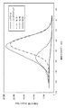
図1は、実施例1に係るマスクブランクの遮光膜に対してX線光電子分光分析を行った結果のうち、内部領域の範囲内にある所定深さにおけるSi2pナロースペクトルを示す図である。同図に示すように、Si2pナロースペクトルに対し、Si−Si結合、SiaNb結合およびSi3N4結合のそれぞれにピーク分離を行い、バックグラウンドを差し引いた面積をそれぞれ算出し、Si−Si結合、SiaNb結合およびSi3N4結合の存在数の比率を算出した。その結果、Si−Si結合の存在数の比率が0.746、SiaNb結合の存在数の比率が0.254、Si3N4結合の存在数の比率が0.000であった。すなわち、Si3N4結合の存在数を、Si3N4結合、SiaNb結合およびSi−Si結合の合計存在数で除した比率が0.04以下という条件と、SiaNb結合の存在数を、Si3N4結合、SiaNb結合およびSi−Si結合の合計存在数で除した比率が0.1以上という条件のいずれをも満たすものであった(前者の条件は0.000で満たし、後者の条件は0.254で満たす)。 FIG. 1 is a diagram showing a Si2p narrow spectrum at a predetermined depth within the range of the internal region among the results of X-ray photoelectron spectroscopy analysis on the light-shielding film of the mask blank according to Example 1. As shown in the figure, with respect Si2p narrow spectrum, Si-Si bonds performs peak separation to each of Si a N b binding and Si 3 N 4 binding to calculate the area obtained by subtracting the background, respectively, Si- The ratio of the abundance of Si bond, Si a N b bond and Si 3 N 4 bond was calculated. As a result, the ratio of the number of existing Si—Si bonds was 0.746, the ratio of the number of existing Si a N b bonds was 0.254, and the ratio of the number of existing Si 3 N 4 bonds was 0.000. That is, the existence number the Si 3 N 4 bond, Si 3 N 4 bond, and provided that the ratio obtained by dividing the Si a N b bond and Si-Si total number of existing bonds 0.04, Si a N b binding The ratio of the existence number of Si 3 N 4 bond, Si a N b bond, and Si-Si bond divided by the total number of abundance is 0.1 or more (the former condition is It is satisfied with 0.000, and the latter condition is satisfied with 0.254).
また、取得した遮光膜の各深さのSi2pナロースペクトルのうち、遮光膜の内部領域に該当する図1に図示した以外の深さの各Si2pナロースペクトルに対して、同様の手順でSi−Si結合、SiaNb結合およびSi3N4結合の存在数の比率を算出した。その結果、いずれの内部領域の深さのSi−Si結合、SiaNb結合およびSi3N4結合の存在数の比率においても、図1に図示した深さのSi−Si結合、SiaNb結合およびSi3N4結合の存在数の比率と同様の傾向を有していた。また、いずれも、上述した存在数の比率に関する2つの条件を満たすものであった。 Further, among the acquired Si2p narrow spectra at each depth of the light-shielding film, Si-Si is applied to each Si2p narrow spectrum at a depth other than that shown in FIG. 1 corresponding to the internal region of the light-shielding film by the same procedure. The ratio of the abundance of bonds, Si a N b bonds and Si 3 N 4 bonds was calculated. As a result, the ratio of the abundance of Si-Si bond, Si a N b bond and Si 3 N 4 bond at the depth of any of the internal regions also shows the Si-Si bond and Si a at the depth shown in FIG. It had a tendency similar to the ratio of the number of N b bonds and Si 3 N 4 bonds present. In addition, all of them satisfy the above-mentioned two conditions regarding the ratio of the number of existence.
また、これらのX線光電子分光分析の結果から、この遮光膜の内部領域の平均の組成は、Si:N:O=75.5:23.2:1.3(原子%比)であることがわかった。なお、このX線光電子分光分析では、X線にAlKα線(1486.6eV)を用い、光電子の検出領域は、200μmφ、取り出し角度が45degの条件で行った(以降の実施例2〜5、比較例1〜2も同様。)。 Further, from the results of these X-ray photoelectron spectroscopy, the average composition of the internal region of this light-shielding film is Si: N: O = 75.5: 23.2: 1. It was found to be 3 (atomic% ratio). In this X-ray photoelectron spectroscopic analysis, AlKα rays (1486.6 eV) were used as X-rays, the photoelectron detection region was 200 μmφ, and the extraction angle was 45 deg (following Examples 2 to 5, comparison). The same applies to Examples 1 and 2).
次に、枚葉式DCスパッタ装置内に加熱処理後の遮光膜2が形成された透光性基板1を設置し、クロム(Cr)ターゲットを用い、アルゴン(Ar)と窒素(N2)との混合ガス雰囲気で反応性スパッタリング(DCスパッタリング)を行い、膜厚5nmのCrN膜からなるハードマスク膜3を成膜した。XPSで測定したこの膜の膜組成比は、Crが75原子%、Nが25原子%であった。そして、遮光膜2で行った加熱処理より低い温度(280℃)で熱処理を行い、ハードマスク膜3の応力調整を行った。
Next, a
以上の手順により、透光性基板1上に、遮光膜2およびハードマスク膜3が積層した構造を備えるマスクブランク100を製造した。
Through the above procedure, a mask blank 100 having a structure in which a light-shielding
[転写用マスクの製造]
次に、この実施例1のマスクブランク100を用い、以下の手順で実施例1の転写用マスク(バイナリマスク)200を製造した。
まず、実施例1のマスクブランク100(図6(a)参照)を準備し、ハードマスク膜3の表面に接して、電子線描画用化学増幅型レジストからなるレジスト膜を膜厚80nmで形成した。次に、このレジスト膜に対して、遮光膜2に形成すべき転写パターンを電子線描画し、所定の現像処理および洗浄処理を行い、レジストパターン4aを形成した(図6(b)参照)。なお、このとき、電子線描画したレジストパターン4aには、遮光膜2に黒欠陥が形成されるように、本来形成されるべき遮光膜パターンのほかにプログラム欠陥を加えておいた。
[Manufacturing of transfer mask]
Next, using the
First, the
次に、レジストパターン4aをマスクとし、塩素と酸素との混合ガス(ガス流量比 Cl2:O2=4:1)を用いたドライエッチングを行い、ハードマスク膜3にパターン(ハードマスクパターン3a)を形成した(図6(c)参照)。
Next, using the resist
次に、レジストパターン4aを除去した(図6(d)参照)。続いて、ハードマスクパターン3aをマスクとし、フッ素系ガス(SF6とHeの混合ガス)を用いたドライエッチングを行い、遮光膜2にパターン(遮光膜パターン2a)を形成した(図6(e)参照)。
Next, the resist
その後、硝酸第二セリウムアンモニウムと過塩素酸を含むクロムエッチング液を用いてハードマスクパターン3aを除去し、洗浄等の所定の処理を経て、転写用マスク200を得た(図6(f)参照)。
Then, the
製造した実施例1の転写用マスク200に対してマスク検査装置によってマスクパターンの検査を行ったところ、プログラム欠陥を配置していた箇所の遮光膜パターン2aに黒欠陥の存在が確認された。その黒欠陥部分に対してEB欠陥修正を行ったところ、透光性基板1に対する遮光膜パターン2aの修正レート比(透光性基板1の修正レートに対する遮光膜パターン2aの修正レート)が十分に高く、透光性基板1の表面へのエッチングを最小限にとどめることができた。
When the mask pattern of the manufactured
次に、このEB欠陥修正後の実施例1の転写用マスク200に対し、AIMS193(Carl Zeiss社製)を用いて、波長193nmの露光光で半導体デバイス上のレジスト膜に露光転写したときにおける転写像のシミュレーションを行った。このシミュレーションの露光転写像を検証したところ、設計仕様を十分に満たしていた。また、EB欠陥修正を行った部分の転写像は、それ以外の領域の転写像に比べてそん色のないものであった。この結果から、実施例1の転写用マスク200に対し、遮光膜パターン2aの黒欠陥部分に対してEB欠陥修正を行った場合に、透光性基板1の表面荒れの発生を抑制でき、かつ遮光膜パターン2aに自発性エッチングが発生することを抑制できるといえる。また、EB欠陥修正を行った後の実施例1の転写用マスク200を露光装置のマスクステージにセットし、半導体デバイス上のレジスト膜に露光転写した場合でも、最終的に半導体デバイス上に形成される回路パターンは高精度で形成できるといえる。このため、実施例1の転写用マスクの製造方法で製造された転写用マスク200は転写精度の高い転写用マスクとなるといえる。
Next, transfer when the
(実施例2)
[マスクブランクの製造]
実施例2のマスクブランクは、遮光膜を下記のようにした以外は、実施例1のマスクブランク100と同様の手順で製造された。
(Example 2)
[Manufacturing of mask blank]
The mask blank of Example 2 was manufactured in the same procedure as the
実施例2の遮光膜の形成方法は以下の通りである。
枚葉式RFスパッタ装置内に透光性基板1を設置し、ケイ素(Si)ターゲットを用い、アルゴン(Ar)、窒素(N2)およびヘリウム(He)の混合ガス(流量比 Ar:N2:He=30:2.3:100)をスパッタリングガスとし、RF電源による反応性スパッタリング(RFスパッタリング)により、透光性基板1上に、ケイ素および窒素からなる遮光膜2を41.5nmの厚さで形成した。また、スパッタリング時のRF電源の電力は1500Wとした。
The method of forming the light-shielding film of Example 2 is as follows.
A
実施例1と同様に、この遮光膜2が形成された透光性基板1に対し加熱処理を行い、加熱処理後の遮光膜2の光学濃度(OD)を測定したところ、その値は2.58であった。この結果から、実施例2のマスクブランクは、必要とされる遮光性能を有している。
Similar to Example 1, the
実施例1と同様に、別の透光性基板の主表面上に、上記の実施例2の遮光膜2と同じ成膜条件で別の遮光膜を形成し、さらに同じ条件で加熱処理を行った。次に、実施例1と同様の手順で、実施例2に係る加熱処理後の別の透光性基板の遮光膜に対して、X線光電子分光分析を行った。さらに、取得した遮光膜の各深さのSi2pナロースペクトルのうち、遮光膜の内部領域に該当する所定深さにおけるSi2pナロースペクトルを基に、実施例1と同様の手順によって、Si−Si結合、SiaNb結合およびSi3N4結合の存在数の比率を算出した。その結果、Si−Si結合の存在数の比率が0.898、SiaNb結合の存在数の比率が0.102、Si3N4結合の存在数の比率が0.000であった。すなわち、Si3N4結合の存在数を、Si3N4結合、SiaNb結合およびSi−Si結合の合計存在数で除した比率が0.04以下という条件と、SiaNb結合の存在数を、Si3N4結合、SiaNb結合およびSi−Si結合の合計存在数で除した比率が0.1以上という条件のいずれをも満たすものであった(前者の条件は0.000で満たし、後者の条件は0.102で満たす)。
Similar to Example 1, another light-shielding film is formed on the main surface of another translucent substrate under the same film-forming conditions as the light-shielding
また、実施例1と同様に、実施例2において取得した遮光膜の各深さのSi2pナロースペクトルのうち、遮光膜の内部領域に該当する上記の所定深さ以外の深さの各Si2pナロースペクトルに対して、同様の手順でSi−Si結合、SiaNb結合およびSi3N4結合の存在数の比率を算出した。いずれの内部領域の深さのSi−Si結合、SiaNb結合およびSi3N4結合の存在数の比率においても、上記の所定深さのSi−Si結合、SiaNb結合およびSi3N4結合の存在数の比率と同様の傾向を有していた。また、いずれも、上述した存在数の比率に関する2つの条件を満たすものであった。
その後、実施例1と同様の手順で、透光性基板1上に、遮光膜2およびハードマスク膜3が積層した構造を備えるマスクブランク100を製造した。
Further, similarly to Example 1, among the Si2p narrow spectra of each depth of the light-shielding film acquired in Example 2, each Si2p narrow spectrum of a depth other than the above-mentioned predetermined depth corresponding to the internal region of the light-shielding film is obtained. respect, the same procedure with Si-Si bond was calculated Si a N b binding and Si 3 N 4 present the ratio of the number of bonds. The ratio of the abundance of Si-Si bond, Si a N b bond and Si 3 N 4 bond at the depth of any internal region also determines the above-mentioned Si-Si bond, Si a N b bond and Si at a predetermined depth. It had a tendency similar to the ratio of the number of 3 N 4 bonds present. In addition, all of them satisfy the above-mentioned two conditions regarding the ratio of the number of existence.
Then, in the same procedure as in Example 1, a mask blank 100 having a structure in which a light-shielding
[転写用マスクの製造]
次に、この実施例2のマスクブランクを用い、実施例1と同様の手順で、実施例2の転写用マスク(バイナリマスク)を製造した。
製造した実施例1の転写用マスク200に対してマスク検査装置によってマスクパターンの検査を行ったところ、プログラム欠陥を配置していた箇所の遮光膜パターン2aに黒欠陥の存在が確認された。その黒欠陥部分に対してEB欠陥修正を行ったところ、透光性基板1に対する遮光膜パターン2aの修正レート比が十分に高く、透光性基板1の表面へのエッチングを最小限にとどめることができた。
[Manufacturing of transfer mask]
Next, using the mask blank of Example 2, a transfer mask (binary mask) of Example 2 was manufactured by the same procedure as in Example 1.
When the mask pattern of the manufactured
このEB欠陥修正後の実施例2の転写用マスク200に対し、AIMS193(Carl Zeiss社製)を用いて、波長193nmの露光光で半導体デバイス上のレジスト膜に露光転写したときにおける転写像のシミュレーションを行った。このシミュレーションの露光転写像を検証したところ、設計仕様を十分に満たしていた。また、EB欠陥修正を行った部分の転写像は、それ以外の領域の転写像に比べてそん色のないものであった。この結果から、実施例2の転写用マスク200に対し、遮光膜パターン2aの黒欠陥部分に対してEB欠陥修正を行った場合に、透光性基板1の表面荒れの発生を抑制でき、かつ遮光膜パターン2aに自発性エッチングが発生することを抑制できるといえる。また、EB欠陥修正を行った後の実施例2の転写用マスク200を露光装置のマスクステージにセットし、半導体デバイス上のレジスト膜に露光転写した場合でも、最終的に半導体デバイス上に形成される回路パターンは高精度で形成できるといえる。このため、実施例2の転写用マスクの製造方法で製造された転写用マスク200は転写精度の高い転写用マスクとなるといえる。
Simulation of a transfer image when the
(実施例3)
[マスクブランクの製造]
実施例3のマスクブランクは、遮光膜を下記のようにした以外は、実施例1のマスクブランク100と同様の手順で製造された。
(Example 3)
[Manufacturing of mask blank]
The mask blank of Example 3 was produced in the same procedure as the
実施例3の遮光膜の形成方法は以下の通りである。
枚葉式RFスパッタ装置内に透光性基板1を設置し、ケイ素(Si)ターゲットを用い、アルゴン(Ar)、窒素(N2)およびヘリウム(He)の混合ガス(流量比 Ar:N2:He=30:5.8:100)をスパッタリングガスとし、RF電源による反応性スパッタリング(RFスパッタリング)により、透光性基板1上に、ケイ素および窒素からなる遮光膜2を52.4nmの厚さで形成した。また、スパッタリング時のRF電源の電力は1500Wとした。
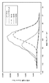
The method of forming the light-shielding film of Example 3 is as follows.
A
実施例1と同様に、この遮光膜2が形成された透光性基板1に対し加熱処理を行い、加熱処理後の遮光膜2の光学濃度(OD)を測定したところ、その値は3.05であった。この結果から、実施例3のマスクブランクは、必要とされる高い遮光性能を有している。
Similar to Example 1, the
実施例1と同様に、別の透光性基板の主表面上に、上記の実施例3の遮光膜2と同じ成膜条件で別の遮光膜を形成し、さらに同じ条件で加熱処理を行った。次に、実施例1と同様の手順で、実施例3に係る加熱処理後の別の透光性基板の遮光膜に対して、X線光電子分光分析を行った。さらに、取得した遮光膜の各深さのSi2pナロースペクトルのうち、遮光膜の内部領域に該当する所定深さにおけるSi2pナロースペクトル(図2参照)を基に、実施例1と同様の手順によって、Si−Si結合、SiaNb結合およびSi3N4結合の存在数の比率を算出した。その結果、Si−Si結合の存在数の比率が0.605、SiaNb結合の存在数の比率が0.373、Si3N4結合の存在数の比率が0.022であった。すなわち、Si3N4結合の存在数を、Si3N4結合、SiaNb結合およびSi−Si結合の合計存在数で除した比率が0.04以下という条件と、SiaNb結合の存在数を、Si3N4結合、SiaNb結合およびSi−Si結合の合計存在数で除した比率が0.1以上という条件のいずれをも満たすものであった(前者の条件は0.022で満たし、後者の条件は0.373で満たす)。
Similar to Example 1, another light-shielding film is formed on the main surface of another translucent substrate under the same film-forming conditions as the light-shielding
また、実施例1と同様に、実施例3において取得した遮光膜の各深さのSi2pナロースペクトルのうち、遮光膜の内部領域に該当する上記の所定深さ以外の深さの各Si2pナロースペクトルに対して、同様の手順でSi−Si結合、SiaNb結合およびSi3N4結合の存在数の比率を算出した。いずれの内部領域の深さのSi−Si結合、SiaNb結合およびSi3N4結合の存在数の比率においても、上記の所定深さのSi−Si結合、SiaNb結合およびSi3N4結合の存在数の比率と同様の傾向を有していた。また、いずれも、上述した存在数の比率に関する2つの条件を満たすものであった。
その後、実施例1と同様の手順で、透光性基板1上に、遮光膜2およびハードマスク膜3が積層した構造を備えるマスクブランク100を製造した。
Further, similarly to Example 1, among the Si2p narrow spectra of each depth of the light-shielding film acquired in Example 3, each Si2p narrow spectrum of a depth other than the above-mentioned predetermined depth corresponding to the internal region of the light-shielding film is obtained. respect, the same procedure with Si-Si bond was calculated Si a N b binding and Si 3 N 4 present the ratio of the number of bonds. The ratio of the abundance of Si-Si bond, Si a N b bond and Si 3 N 4 bond at the depth of any internal region also determines the above-mentioned Si-Si bond, Si a N b bond and Si at a predetermined depth. It had a tendency similar to the ratio of the number of 3 N 4 bonds present. In addition, all of them satisfy the above-mentioned two conditions regarding the ratio of the number of existence.
Then, in the same procedure as in Example 1, a mask blank 100 having a structure in which a light-shielding
[転写用マスクの製造]
次に、この実施例3のマスクブランクを用い、実施例1と同様の手順で、実施例3の転写用マスク(バイナリマスク)を製造した。
製造した実施例3の転写用マスク200に対してマスク検査装置によってマスクパターンの検査を行ったところ、プログラム欠陥を配置していた箇所の遮光膜パターン2aに黒欠陥の存在が確認された。その黒欠陥部分に対してEB欠陥修正を行ったところ、透光性基板1に対する遮光膜パターン2aの修正レート比が十分に高く、透光性基板1の表面へのエッチングを最小限にとどめることができた。
[Manufacturing of transfer mask]
Next, using the mask blank of Example 3, a transfer mask (binary mask) of Example 3 was manufactured by the same procedure as in Example 1.
When the mask pattern of the manufactured
このEB欠陥修正後の実施例3の転写用マスク200に対し、AIMS193(Carl Zeiss社製)を用いて、波長193nmの露光光で半導体デバイス上のレジスト膜に露光転写したときにおける転写像のシミュレーションを行った。このシミュレーションの露光転写像を検証したところ、設計仕様を十分に満たしていた。また、EB欠陥修正を行った部分の転写像は、それ以外の領域の転写像に比べてそん色のないものであった。この結果から、実施例3の転写用マスク200に対し、遮光膜パターン2aの黒欠陥部分に対してEB欠陥修正を行った場合に、透光性基板1の表面荒れの発生を抑制でき、かつ遮光膜パターン2aに自発性エッチングが発生することを抑制できるといえる。また、EB欠陥修正を行った後の実施例3の転写用マスク200を露光装置のマスクステージにセットし、半導体デバイス上のレジスト膜に露光転写した場合でも、最終的に半導体デバイス上に形成される回路パターンは高精度で形成できるといえる。このため、実施例3の転写用マスクの製造方法で製造された転写用マスク200は転写精度の高い転写用マスクとなるといえる。
Simulation of a transfer image when the
(実施例4)
[マスクブランクの製造]
実施例4のマスクブランクは、遮光膜を下記のようにした以外は、実施例1のマスクブランク100と同様の手順で製造された。
(Example 4)
[Manufacturing of mask blank]
The mask blank of Example 4 was produced in the same procedure as the
実施例4の遮光膜の形成方法は以下の通りである。
枚葉式RFスパッタ装置内に透光性基板1を設置し、ケイ素(Si)ターゲットを用い、アルゴン(Ar)、窒素(N2)およびヘリウム(He)の混合ガス(流量比 Ar:N2:He=30:6.6:100)をスパッタリングガスとし、RF電源による反応性スパッタリング(RFスパッタリング)により、透光性基板1上に、ケイ素および窒素からなる遮光膜2を45.1nmの厚さで形成した。また、スパッタリング時のRF電源の電力は1500Wとした。
The method of forming the light-shielding film of Example 4 is as follows.
A
実施例1と同様に、この遮光膜2が形成された透光性基板1に対し加熱処理を行い、加熱処理後の遮光膜2の光学濃度(OD)を測定したところ、その値は2.54であった。この結果から、実施例4のマスクブランクは、必要とされる遮光性能を有している。
Similar to Example 1, the
実施例1と同様に、別の透光性基板の主表面上に、上記の実施例4の遮光膜2と同じ成膜条件で別の遮光膜を形成し、さらに同じ条件で加熱処理を行った。次に、実施例1と同様の手順で、実施例4に係る加熱処理後の別の透光性基板の遮光膜に対して、X線光電子分光分析を行った。さらに、取得した遮光膜の各深さのSi2pナロースペクトルのうち、遮光膜の内部領域に該当する所定深さにおけるSi2pナロースペクトルを基に、実施例1と同様の手順によって、Si−Si結合、SiaNb結合およびSi3N4結合の存在数の比率を算出した。その結果、Si−Si結合の存在数の比率が0.584、SiaNb結合の存在数の比率が0.376、Si3N4結合の存在数の比率が0.040であった。すなわち、Si3N4結合の存在数を、Si3N4結合、SiaNb結合およびSi−Si結合の合計存在数で除した比率が0.04以下という条件と、SiaNb結合の存在数を、Si3N4結合、SiaNb結合およびSi−Si結合の合計存在数で除した比率が0.1以上という条件のいずれをも満たすものであった(前者の条件は0.040で満たし、後者の条件は0.376で満たす)。
Similar to Example 1, another light-shielding film is formed on the main surface of another translucent substrate under the same film-forming conditions as the light-shielding
また、実施例1と同様に、実施例4において取得した遮光膜の各深さのSi2pナロースペクトルのうち、遮光膜の内部領域に該当する上記の所定深さ以外の深さの各Si2pナロースペクトルに対して、同様の手順でSi−Si結合、SiaNb結合およびSi3N4結合の存在数の比率を算出した。いずれの内部領域の深さのSi−Si結合、SiaNb結合およびSi3N4結合の存在数の比率においても、上記の所定深さのSi−Si結合、SiaNb結合およびSi3N4結合の存在数の比率と同様の傾向を有していた。また、いずれも、上述した存在数の比率に関する2つの条件を満たすものであった。
その後、実施例1と同様の手順で、透光性基板1上に、遮光膜2およびハードマスク膜3が積層した構造を備えるマスクブランク100を製造した。
Further, similarly to Example 1, among the Si2p narrow spectra of each depth of the light-shielding film acquired in Example 4, each Si2p narrow spectrum of a depth other than the above-mentioned predetermined depth corresponding to the internal region of the light-shielding film is obtained. respect, the same procedure with Si-Si bond was calculated Si a N b binding and Si 3 N 4 present the ratio of the number of bonds. The ratio of the abundance of Si-Si bond, Si a N b bond and Si 3 N 4 bond at the depth of any internal region also determines the above-mentioned Si-Si bond, Si a N b bond and Si at a predetermined depth. It had a tendency similar to the ratio of the number of 3 N 4 bonds present. In addition, all of them satisfy the above-mentioned two conditions regarding the ratio of the number of existence.
Then, in the same procedure as in Example 1, a mask blank 100 having a structure in which a light-shielding
[転写用マスクの製造]
次に、この実施例4のマスクブランクを用い、実施例1と同様の手順で、実施例4の転写用マスク(バイナリマスク)を製造した。
製造した実施例1の転写用マスク200に対してマスク検査装置によってマスクパターンの検査を行ったところ、プログラム欠陥を配置していた箇所の遮光膜パターン2aに黒欠陥の存在が確認された。その黒欠陥部分に対してEB欠陥修正を行ったところ、透光性基板1に対する遮光膜パターン2aの修正レート比が十分に高く、透光性基板1の表面へのエッチングを最小限にとどめることができた。
[Manufacturing of transfer mask]
Next, using the mask blank of Example 4, a transfer mask (binary mask) of Example 4 was manufactured by the same procedure as in Example 1.
When the mask pattern of the manufactured
このEB欠陥修正後の実施例4の転写用マスク200に対し、AIMS193(Carl Zeiss社製)を用いて、波長193nmの露光光で半導体デバイス上のレジスト膜に露光転写したときにおける転写像のシミュレーションを行った。このシミュレーションの露光転写像を検証したところ、設計仕様を十分に満たしていた。また、EB欠陥修正を行った部分の転写像は、それ以外の領域の転写像に比べてそん色のないものであった。この結果から、実施例4の転写用マスク200に対し、遮光膜パターン2aの黒欠陥部分に対してEB欠陥修正を行った場合に、透光性基板1の表面荒れの発生を抑制でき、かつ遮光膜パターン2aに自発性エッチングが発生することを抑制できるといえる。また、EB欠陥修正を行った後の実施例4の転写用マスク200を露光装置のマスクステージにセットし、半導体デバイス上のレジスト膜に露光転写した場合でも、最終的に半導体デバイス上に形成される回路パターンは高精度で形成できるといえる。このため、実施例4の転写用マスクの製造方法で製造された転写用マスク200は転写精度の高い転写用マスクとなるといえる。
Simulation of a transfer image when the
(実施例5)
[マスクブランクの製造]
実施例5のマスクブランクは、遮光膜を下記のようにした以外は、実施例1のマスクブランク100と同様の手順で製造された。
(Example 5)
[Manufacturing of mask blank]
The mask blank of Example 5 was produced in the same procedure as the
実施例5の遮光膜の形成方法は以下の通りである。
枚葉式RFスパッタ装置内に透光性基板1を設置し、ケイ素(Si)ターゲットを用い、アルゴン(Ar)、窒素(N2)およびヘリウム(He)の混合ガス(流量比 Ar:N2:He=30:7.0:100)をスパッタリングガスとし、RF電源による反応性スパッタリング(RFスパッタリング)により、透光性基板1上に、ケイ素および窒素からなる遮光膜2を52.1nmの厚さで形成した。また、スパッタリング時のRF電源の電力は1500Wとした。ここで、実施例5における枚葉式RFスパッタ装置は、実施例1〜4で用いたものと同じ設計仕様ではあるが、実施例1〜4とは別の枚葉式RFスパッタ装置である。
The method of forming the light-shielding film of Example 5 is as follows.
A
実施例1と同様に、この遮光膜2が形成された透光性基板1に対し加熱処理を行い、加熱処理後の遮光膜2の光学濃度(OD)を測定したところ、その値は3.04であった。この結果から、実施例5のマスクブランクは、必要とされる高い遮光性能を有している。
Similar to Example 1, the
実施例1と同様に、別の透光性基板の主表面上に、上記の実施例5の遮光膜2と同じ成膜条件で別の遮光膜を形成し、さらに同じ条件で加熱処理を行った。次に、実施例1と同様の手順で、実施例5に係る加熱処理後の別の透光性基板の遮光膜に対して、X線光電子分光分析を行った。さらに、取得した遮光膜の各深さのSi2pナロースペクトルのうち、遮光膜の内部領域に該当する所定深さにおけるSi2pナロースペクトル(図3参照)を基に、実施例1と同様の手順によって、Si−Si結合、SiaNb結合およびSi3N4結合の存在数の比率を算出した。その結果、Si−Si結合の存在数の比率が0.700、SiaNb結合の存在数の比率が0.284、Si3N4結合の存在数の比率が0.016であった。すなわち、Si3N4結合の存在数を、Si3N4結合、SiaNb結合およびSi−Si結合の合計存在数で除した比率が0.04以下という条件と、SiaNb結合の存在数を、Si3N4結合、SiaNb結合およびSi−Si結合の合計存在数で除した比率が0.1以上という条件のいずれをも満たすものであった(前者の条件は0.016で満たし、後者の条件は0.284で満たす)。
Similar to Example 1, another light-shielding film is formed on the main surface of another translucent substrate under the same film-forming conditions as the light-shielding
また、実施例1と同様に、実施例5において取得した遮光膜の各深さのSi2pナロースペクトルのうち、遮光膜の内部領域に該当する上記の所定深さ以外の深さの各Si2pナロースペクトルに対して、同様の手順でSi−Si結合、SiaNb結合およびSi3N4結合の存在数の比率を算出した。いずれの内部領域の深さのSi−Si結合、SiaNb結合およびSi3N4結合の存在数の比率においても、上記の所定深さのSi−Si結合、SiaNb結合およびSi3N4結合の存在数の比率と同様の傾向を有していた。また、いずれも、上述した存在数の比率に関する2つの条件を満たすものであった。
その後、実施例1と同様の手順で、透光性基板1上に、遮光膜2およびハードマスク膜3が積層した構造を備えるマスクブランク100を製造した。
Further, similarly to Example 1, among the Si2p narrow spectra of each depth of the light-shielding film acquired in Example 5, each Si2p narrow spectrum of a depth other than the above-mentioned predetermined depth corresponding to the internal region of the light-shielding film is obtained. respect, the same procedure with Si-Si bond was calculated Si a N b binding and Si 3 N 4 present the ratio of the number of bonds. The ratio of the abundance of Si-Si bond, Si a N b bond and Si 3 N 4 bond at the depth of any internal region also determines the above-mentioned Si-Si bond, Si a N b bond and Si at a predetermined depth. It had a tendency similar to the ratio of the number of 3 N 4 bonds present. In addition, all of them satisfy the above-mentioned two conditions regarding the ratio of the number of existence.
Then, in the same procedure as in Example 1, a mask blank 100 having a structure in which a light-shielding
[転写用マスクの製造]
次に、この実施例5のマスクブランクを用い、実施例1と同様の手順で、実施例5の転写用マスク(バイナリマスク)を製造した。
製造した実施例5の転写用マスク200に対してマスク検査装置によってマスクパターンの検査を行ったところ、プログラム欠陥を配置していた箇所の遮光膜パターン2aに黒欠陥の存在が確認された。その黒欠陥部分に対してEB欠陥修正を行ったところ、透光性基板1に対する遮光膜パターン2aの修正レート比が十分に高く、透光性基板1の表面へのエッチングを最小限にとどめることができた。
[Manufacturing of transfer mask]
Next, using the mask blank of Example 5, a transfer mask (binary mask) of Example 5 was manufactured by the same procedure as in Example 1.
When the mask pattern of the manufactured
このEB欠陥修正後の実施例5の転写用マスク200に対し、AIMS193(Carl Zeiss社製)を用いて、波長193nmの露光光で半導体デバイス上のレジスト膜に露光転写したときにおける転写像のシミュレーションを行った。このシミュレーションの露光転写像を検証したところ、設計仕様を十分に満たしていた。また、EB欠陥修正を行った部分の転写像は、それ以外の領域の転写像に比べてそん色のないものであった。この結果から、実施例5の転写用マスク200に対し、遮光膜パターン2aの黒欠陥部分に対してEB欠陥修正を行った場合に、透光性基板1の表面荒れの発生を抑制でき、かつ遮光膜パターン2aに自発性エッチングが発生することを抑制できるといえる。また、EB欠陥修正を行った後の実施例5の転写用マスク200を露光装置のマスクステージにセットし、半導体デバイス上のレジスト膜に露光転写した場合でも、最終的に半導体デバイス上に形成される回路パターンは高精度で形成できるといえる。このため、実施例5の転写用マスクの製造方法で製造された転写用マスク200は転写精度の高い転写用マスクとなるといえる。
Simulation of a transfer image when the
(比較例1)
[マスクブランクの製造]
比較例1のマスクブランクは、遮光膜を下記のようにした以外は、実施例1のマスクブランク100と同様の手順で製造された。
(Comparative Example 1)
[Manufacturing of mask blank]
The mask blank of Comparative Example 1 was produced in the same procedure as the
比較例1の遮光膜の形成方法は以下の通りである。
枚葉式RFスパッタ装置内に透光性基板を設置し、ケイ素(Si)ターゲットを用い、アルゴン(Ar)、窒素(N2)およびヘリウム(He)の混合ガス(流量比 Ar:N2:He=30:7.0:100)をスパッタリングガスとし、RF電源による反応性スパッタリング(RFスパッタリング)により、透光性基板上に、ケイ素および窒素からなる遮光膜を52.8nmの厚さで形成した。また、スパッタリング時のRF電源の電力は1500Wとした。このように、実施例5と同じガス流量、スパッタリングの出力で比較例1の遮光膜を形成した。比較例1における枚葉式RFスパッタ装置は、実施例1〜4で用いたものと同じ枚葉式RFスパッタ装置である。
The method of forming the light-shielding film of Comparative Example 1 is as follows.
A translucent substrate is installed in a single-wafer RF sputtering device, a silicon (Si) target is used, and a mixed gas of argon (Ar), nitrogen (N 2 ) and helium (He) (flow ratio Ar: N 2 : He = 30: 7.0: 100) is used as the sputtering gas, and a light-shielding film made of silicon and nitrogen is formed on a translucent substrate with a thickness of 52.8 nm by reactive sputtering (RF sputtering) using an RF power source. bottom. The power of the RF power supply during sputtering was set to 1500 W. In this way, the light-shielding film of Comparative Example 1 was formed with the same gas flow rate and sputtering output as in Example 5. The single-wafer RF sputtering apparatus in Comparative Example 1 is the same single-wafer RF sputtering apparatus used in Examples 1 to 4.
実施例1と同様に、この遮光膜が形成された透光性基板に対し加熱処理を行い、加熱処理後の遮光膜の光学濃度(OD)を測定したところ、その値は2.98であった。この結果から、比較例1のマスクブランクは、必要とされる遮光性能を有している。 Similar to Example 1, the translucent substrate on which the light-shielding film was formed was heat-treated, and the optical density (OD) of the light-shielding film after the heat treatment was measured. As a result, the value was 2.98. rice field. From this result, the mask blank of Comparative Example 1 has the required light-shielding performance.
実施例1と同様に、別の透光性基板の主表面上に、上記の比較例1の遮光膜と同じ成膜条件で別の遮光膜を形成し、さらに同じ条件で加熱処理を行った。次に、実施例1と同様の手順で、比較例1に係る加熱処理後の別の透光性基板の遮光膜に対して、X線光電子分光分析を行った。さらに、取得した遮光膜の各深さのSi2pナロースペクトルのうち、遮光膜の内部領域に該当する所定深さにおけるSi2pナロースペクトル(図4参照)を基に、実施例1と同様の手順によって、Si−Si結合、SiaNb結合およびSi3N4結合の存在数の比率を算出した。その結果、Si−Si結合の存在数の比率が0.574、SiaNb結合の存在数の比率が0.382、Si3N4結合の存在数の比率が0.044であった。すなわち、SiaNb結合の存在数を、Si3N4結合、SiaNb結合およびSi−Si結合の合計存在数で除した比率が0.1以上という条件は満たすものの、Si3N4結合の存在数を、Si3N4結合、SiaNb結合およびSi−Si結合の合計存在数で除した比率が0.04以下という条件を満たすものではなかった(前者の条件は0.382で満たすものの、後者の条件は0.044で満たさなかった)。 Similar to Example 1, another light-shielding film was formed on the main surface of another translucent substrate under the same film forming conditions as the light-shielding film of Comparative Example 1 above, and further heat-treated under the same conditions. .. Next, X-ray photoelectron spectroscopy was performed on the light-shielding film of another translucent substrate after the heat treatment according to Comparative Example 1 in the same procedure as in Example 1. Further, among the acquired Si2p narrow spectra at each depth of the light-shielding film, based on the Si2p narrow spectrum (see FIG. 4) at a predetermined depth corresponding to the internal region of the light-shielding film, the same procedure as in Example 1 is performed. Si-Si bonds, were calculated Si a N b binding and Si 3 N 4 present the ratio of the number of bonds. As a result, the ratio of the number of existing Si—Si bonds was 0.574, the ratio of the number of existing Si a N b bonds was 0.382, and the ratio of the number of existing Si 3 N 4 bonds was 0.044. That is, the number of existing Si a N b bond, Si 3 N 4 binding, although Si a N b bond and the ratio obtained by dividing the total number of existing Si-Si bonds satisfy the condition of 0.1 or more, Si 3 N It did not satisfy the condition that the ratio of the number of 4 bonds divided by the total number of Si 3 N 4 bonds, Si a N b bonds and Si-Si bonds was 0.04 or less (the former condition was 0). The latter condition was not satisfied with 0.044, although it was satisfied with .382).
また、実施例1と同様に、この比較例1において取得した遮光膜の各深さのSi2pナロースペクトルのうち、遮光膜の内部領域に該当する上記の所定深さ以外の深さの各Si2pナロースペクトルに対して、同様の手順でSi−Si結合、SiaNb結合およびSi3N4結合の存在数の比率を算出した。いずれの内部領域の深さのSi−Si結合、SiaNb結合およびSi3N4結合の存在数の比率においても、上記の所定深さのSi−Si結合、SiaNb結合およびSi3N4結合の存在数の比率と同様の傾向を有していた。また、いずれも、Si3N4結合の存在数を、Si3N4結合、SiaNb結合およびSi−Si結合の合計存在数で除した比率が0.04以下という条件を満たしてはいなかった。 Further, similarly to Example 1, in the Si2p narrow spectrum of each depth of the light-shielding film acquired in Comparative Example 1, each Si2p narrow spectrum having a depth other than the above-mentioned predetermined depth corresponding to the internal region of the light-shielding film is obtained. relative spectrum, the same procedure with Si-Si bond was calculated Si a N b binding and Si 3 N 4 present the ratio of the number of bonds. The ratio of the abundance of Si-Si bond, Si a N b bond and Si 3 N 4 bond at the depth of any internal region also determines the above-mentioned Si-Si bond, Si a N b bond and Si at a predetermined depth. It had a tendency similar to the ratio of the number of 3 N 4 bonds present. Further, Yes Both the existence number the Si 3 N 4 bond, Si 3 N 4 bond, meets the Si a N b bond and Si-Si ratio divided by the total number of existing bonds condition that 0.04 There wasn't.
これらのX線光電子分光分析の結果から、この遮光膜の内部領域の平均の組成は、Si:N:O=68.2:28.8:3.0(原子%比)であることがわかった。
その後、実施例1と同様の手順で、透光性基板上に、遮光膜およびハードマスク膜が積層した構造を備えるマスクブランクを製造した。
From the results of these X-ray photoelectron spectroscopy, it was found that the average composition of the internal region of this light-shielding film was Si: N: O = 68.2: 28.8: 3.0 (atomic% ratio). rice field.
Then, in the same procedure as in Example 1, a mask blank having a structure in which a light-shielding film and a hard mask film were laminated on a translucent substrate was manufactured.
[転写用マスクの製造]
次に、この比較例1のマスクブランクを用い、実施例1と同様の手順で、比較例1の転写用マスク(バイナリマスク)を製造した。
製造した比較例1の転写用マスクに対してマスク検査装置によってマスクパターンの検査を行ったところ、プログラム欠陥を配置していた箇所の遮光膜パターンに黒欠陥の存在が確認された。その黒欠陥部分に対してEB欠陥修正を行ったところ、透光性基板に対する遮光膜パターンの修正レート比が低く、透光性基板の表面へのエッチング(表面荒れ)が進んでいた。
[Manufacturing of transfer mask]
Next, using the mask blank of Comparative Example 1, a transfer mask (binary mask) of Comparative Example 1 was manufactured by the same procedure as in Example 1.
When the mask pattern of the manufactured transfer mask of Comparative Example 1 was inspected by a mask inspection device, the presence of black defects was confirmed in the light-shielding film pattern at the location where the program defects were arranged. When the EB defect was corrected for the black defect portion, the correction rate ratio of the light-shielding film pattern to the translucent substrate was low, and etching (surface roughness) on the surface of the translucent substrate was advanced.
このEB欠陥修正後の比較例1の転写用マスクに対し、AIMS193(Carl Zeiss社製)を用いて、波長193nmの露光光で半導体デバイス上のレジスト膜に露光転写したときにおける転写像のシミュレーションを行った。このシミュレーションの露光転写像を検証したところ、EB欠陥修正を行った部分以外でも、遮光膜にパターンを形成するときのドライエッチングでのエッチングレートの遅さに起因すると見られる遮光膜パターンのCDの低下が発生していた。さらに、EB欠陥修正を行った部分の転写像は、透光性基板の表面荒れの影響等に起因して転写不良が発生するレベルのものであった。この結果から、EB欠陥修正を行った後の比較例1の転写用マスクを露光装置のマスクステージにセットし、半導体デバイス上のレジスト膜に露光転写した場合、最終的に半導体デバイス上に形成される回路パターンには、回路パターンの断線や短絡が発生することが予想される。 Using AIMS193 (manufactured by Carl Zeiss) for the transfer mask of Comparative Example 1 after the EB defect correction, a simulation of a transfer image when exposure transfer was performed on a resist film on a semiconductor device with exposure light having a wavelength of 193 nm was performed. went. When the exposure transfer image of this simulation was verified, it was found that the CD of the light-shielding film pattern, which seems to be caused by the slow etching rate in dry etching when forming the pattern on the light-shielding film, other than the part where the EB defect was corrected. There was a drop. Further, the transfer image of the portion where the EB defect was corrected was at a level at which transfer defects occur due to the influence of surface roughness of the translucent substrate. From this result, when the transfer mask of Comparative Example 1 after the EB defect correction was set on the mask stage of the exposure apparatus and the exposure transfer was performed on the resist film on the semiconductor device, it was finally formed on the semiconductor device. It is expected that the circuit pattern will be broken or short-circuited.
(比較例2)
[マスクブランクの製造]
比較例2のマスクブランクは、遮光膜を下記のようにした以外は、実施例1のマスクブランク100と同様の手順で製造された。
(Comparative Example 2)
[Manufacturing of mask blank]
The mask blank of Comparative Example 2 was produced in the same procedure as the
比較例2の遮光膜の形成方法は以下の通りである。
枚葉式RFスパッタ装置内に透光性基板を設置し、ケイ素(Si)ターゲットを用い、アルゴン(Ar)、窒素(N2)およびヘリウム(He)の混合ガス(流量比 Ar:N2:He=30:2.0:100)をスパッタリングガスとし、RF電源による反応性スパッタリング(RFスパッタリング)により、透光性基板上に、ケイ素および窒素からなる遮光膜を48.0nmの厚さで形成した。また、スパッタリング時のRF電源の電力は1500Wとした。このように、比較例2における枚葉式RFスパッタ装置は、実施例1〜4、比較例1で用いたものと同じ枚葉式RFスパッタ装置である。
The method of forming the light-shielding film of Comparative Example 2 is as follows.
A translucent substrate is installed in a single-wafer RF sputtering device, a silicon (Si) target is used, and a mixed gas of argon (Ar), nitrogen (N 2 ) and helium (He) (flow ratio Ar: N 2 : He = 30: 2.0: 100) was used as the sputtering gas, and a light-shielding film made of silicon and nitrogen was formed with a thickness of 48.0 nm on the translucent substrate by reactive sputtering (RF sputtering) using an RF power source. bottom. The power of the RF power supply during sputtering was set to 1500 W. As described above, the single-wafer RF sputtering apparatus in Comparative Example 2 is the same single-wafer RF sputtering apparatus used in Examples 1 to 4 and Comparative Example 1.
実施例1と同様に、この遮光膜が形成された透光性基板に対し加熱処理を行い、加熱処理後の遮光膜の光学濃度(OD)を測定したところ、その値は3.04であった。この結果から、比較例2のマスクブランクは、必要とされる高い遮光性能を有している。 Similar to Example 1, the translucent substrate on which the light-shielding film was formed was heat-treated, and the optical density (OD) of the light-shielding film after the heat treatment was measured. As a result, the value was 3.04. rice field. From this result, the mask blank of Comparative Example 2 has the required high light-shielding performance.
実施例1と同様に、別の透光性基板の主表面上に、上記の比較例2の遮光膜と同じ成膜条件で別の遮光膜を形成し、さらに同じ条件で加熱処理を行った。次に、実施例1と同様の手順で、比較例2に係る加熱処理後の別の透光性基板の遮光膜に対して、X線光電子分光分析を行った。さらに、取得した遮光膜の各深さのSi2pナロースペクトルのうち、遮光膜の内部領域に該当する所定深さにおけるSi2pナロースペクトルを基に、実施例1と同様の手順によって、Si−Si結合、SiaNb結合およびSi3N4結合の存在数の比率を算出した。その結果、Si−Si結合の存在数の比率が0.978、SiaNb結合の存在数の比率が0.022、Si3N4結合の存在数の比率が0.000であった。すなわち、Si3N4結合の存在数を、Si3N4結合、SiaNb結合およびSi−Si結合の合計存在数で除した比率が0.04以下という条件は満たすものの、SiaNb結合の存在数を、Si3N4結合、SiaNb結合およびSi−Si結合の合計存在数で除した比率が0.1以上という条件を満たすものではなかった(前者の条件は0.000で満たすものの、後者の条件は0.022で満たさなかった)。 Similar to Example 1, another light-shielding film was formed on the main surface of another translucent substrate under the same film forming conditions as the light-shielding film of Comparative Example 2 above, and further heat-treated under the same conditions. .. Next, X-ray photoelectron spectroscopy was performed on the light-shielding film of another translucent substrate after the heat treatment according to Comparative Example 2 in the same procedure as in Example 1. Further, among the acquired Si2p narrow spectra at each depth of the light-shielding film, based on the Si2p narrow spectrum at a predetermined depth corresponding to the internal region of the light-shielding film, Si—Si bonding is performed by the same procedure as in Example 1. The ratio of the abundance of Si a N b bond and Si 3 N 4 bond was calculated. As a result, the ratio of the number of existing Si—Si bonds was 0.978, the ratio of the number of existing Si a N b bonds was 0.022, and the ratio of the number of existing Si 3 N 4 bonds was 0.000. That is, the existence number the Si 3 N 4 bond, Si 3 N 4 binding, although Si a N b bond and the ratio obtained by dividing the total number of existing Si-Si bonds satisfy the condition that 0.04, Si a N It did not satisfy the condition that the ratio of the number of b- bonds divided by the total number of Si 3 N 4 bonds, Si a N b bonds and Si-Si bonds was 0.1 or more (the former condition was 0). The latter condition was not satisfied with 0.022, although it was satisfied with .000).
また、実施例1と同様に、この比較例2において取得した遮光膜の各深さのSi2pナロースペクトルのうち、遮光膜の内部領域に該当する上記の所定深さ以外の深さの各Si2pナロースペクトルに対して、同様の手順でSi−Si結合、SiaNb結合およびSi3N4結合の存在数の比率を算出した。いずれの内部領域の深さのSi−Si結合、SiaNb結合およびSi3N4結合の存在数の比率においても、上記の所定深さのSi−Si結合、SiaNb結合およびSi3N4結合の存在数の比率と同様の傾向を有していた。また、いずれの箇所においても、SiaNb結合の存在数を、Si3N4結合、SiaNb結合およびSi−Si結合の合計存在数で除した比率が0.1以上という条件を満たすものではなかった。
その後、実施例1と同様の手順で、透光性基板上に、遮光膜およびハードマスク膜が積層した構造を備えるマスクブランクを製造した。
Further, similarly to Example 1, in the Si2p narrow spectrum of each depth of the light-shielding film acquired in Comparative Example 2, each Si2p narrow spectrum having a depth other than the above-mentioned predetermined depth corresponding to the internal region of the light-shielding film. relative spectrum, the same procedure with Si-Si bond was calculated Si a N b binding and Si 3 N 4 present the ratio of the number of bonds. The ratio of the abundance of Si-Si bond, Si a N b bond and Si 3 N 4 bond at the depth of any internal region also determines the above-mentioned Si-Si bond, Si a N b bond and Si at a predetermined depth. It had a tendency similar to the ratio of the number of 3 N 4 bonds present. In any location, the number of existing Si a N b bond, Si 3 N 4 bond, the ratio obtained by dividing the Si a N b bond and Si-Si total number of existing bonds the condition that 0.1 or more It didn't meet.
Then, in the same procedure as in Example 1, a mask blank having a structure in which a light-shielding film and a hard mask film were laminated on a translucent substrate was manufactured.
[転写用マスクの製造]
次に、この比較例2のマスクブランクを用い、実施例1と同様の手順で、比較例2の転写用マスク(バイナリマスク)を製造した。
製造した比較例2の転写用マスクに対してマスク検査装置によってマスクパターンの検査を行ったところ、プログラム欠陥を配置していた箇所の遮光膜パターンに黒欠陥の存在が確認された。その黒欠陥部分に対してEB欠陥修正を行ったところ、修正レートが速すぎてアンダーカットが発生していた。さらに、黒欠陥部分の周囲の遮光膜パターンの側壁がEB欠陥修正時に供給される非励起状態のXeF2ガスが接触することによってエッチングされる現象、すなわち自発性エッチングが進んでいた。
[Manufacturing of transfer mask]
Next, using the mask blank of Comparative Example 2, in the same manner as in Example 1 to produce a transfer mask of Comparative Example 2 (binary mask).
When the mask pattern of the manufactured transfer mask of Comparative Example 2 was inspected by a mask inspection device, the presence of black defects was confirmed in the light-shielding film pattern at the location where the program defects were arranged. When the EB defect was corrected for the black defect portion, the correction rate was too fast and an undercut occurred. Further, a phenomenon in which the side wall of the light-shielding film pattern around the black defect portion is etched by contact with the non-excited XeF 2 gas supplied at the time of EB defect correction, that is, spontaneous etching has progressed.
このEB欠陥修正後の比較例2の転写用マスクに対し、AIMS193(Carl Zeiss社製)を用いて、波長193nmの露光光で半導体デバイス上のレジスト膜に露光転写したときにおける転写像のシミュレーションを行った。このシミュレーションの露光転写像を検証したところ、EB欠陥修正を行った部分での透光性基板1の表面荒れは発生していなかった。しかし、EB欠陥修正を行った部分の周囲の転写像は、自発性エッチングの影響等に起因して転写不良が発生するレベルのものであった。この結果から、EB欠陥修正を行った後の比較例2の位相シフトマスクを露光装置のマスクステージにセットし、半導体デバイス上のレジスト膜に露光転写した場合、最終的に半導体デバイス上に形成される回路パターンには、回路パターンの断線や短絡が発生することが予想される。
For the transfer mask of Comparative Example 2 after the EB defect correction, AIMS193 (manufactured by Carl Zeiss) was used to simulate a transfer image when exposure transfer was performed on a resist film on a semiconductor device with exposure light having a wavelength of 193 nm. went. When the exposure transfer image of this simulation was verified, the surface roughness of the
1 透光性基板
2 遮光膜
2a 遮光膜パターン
21 基板近傍領域
22 内部領域
23 表層領域
3 ハードマスク膜
3a ハードマスクパターン
4a レジストパターン
100 マスクブランク
200 転写用マスク(バイナリマスク)
1
Claims (9)
前記遮光膜は、ケイ素と窒素とからなる材料、または半金属元素および非金属元素から選ばれる1以上の元素とケイ素と窒素とからなる材料で形成され、
前記遮光膜の前記透光性基板との界面の近傍領域と前記遮光膜の前記透光性基板とは反対側の表層領域を除いた内部領域におけるSi3N4結合の存在数を、Si3N4結合、SiaNb結合(ただし、b/[a+b]<4/7)およびSi−Si結合の合計存在数で除した比率が0.04以下であり、
前記遮光膜の前記内部領域におけるSiaNb結合の存在数を、Si3N4結合、SiaNb結合およびSi−Si結合の合計存在数で除した比率が0.1以上であり、
前記遮光膜の前記内部領域は、ケイ素および窒素の合計含有量が98原子%以上であり、
前記表層領域は、前記遮光膜における前記透光性基板とは反対側の表面から前記透光性基板側に向かって5nmの深さまでの範囲にわたる領域であり、
前記近傍領域は、前記透光性基板との界面から前記表層領域側に向かって5nmの深さまでの範囲にわたる領域である
ことを特徴とするマスクブランク。 A mask blank provided with a light-shielding film for forming a transfer pattern on a translucent substrate.
The light-shielding film is formed of a material composed of silicon and nitrogen, or a material composed of one or more elements selected from metalloid elements and non-metal elements, and silicon and nitrogen.
The number of Si 3 N 4 bonds present in the internal region excluding the region near the interface of the light-shielding film with the translucent substrate and the surface layer region on the side opposite to the translucent substrate of the light-shielding film is determined by Si 3. The ratio divided by the total number of N 4 bonds, Si a N b bonds (however, b / [a + b] <4/7) and Si-Si bonds is 0.04 or less.
The number of existing Si a N b bond in the interior region of the light shielding film, Si 3 N 4 bond, Si a N b bond and the ratio obtained by dividing the total number of existing Si-Si bonds Ri der 0.1 or higher ,
The internal region of the light-shielding film has a total content of silicon and nitrogen of 98 atomic% or more.
The surface layer region is a region extending from the surface of the light-shielding film opposite to the translucent substrate to a depth of 5 nm toward the translucent substrate side.
The mask blank is a region extending from an interface with the translucent substrate to a depth of 5 nm toward the surface layer region side.
Priority Applications (6)
| Application Number | Priority Date | Filing Date | Title |
|---|---|---|---|
| JP2017107767A JP6932552B2 (en) | 2017-05-31 | 2017-05-31 | Mask blank, transfer mask manufacturing method and semiconductor device manufacturing method |
| KR1020197030979A KR102565111B1 (en) | 2017-05-31 | 2018-05-15 | Mask blank, transfer mask manufacturing method, and semiconductor device manufacturing method |
| US16/615,542 US20200166833A1 (en) | 2017-05-31 | 2018-05-15 | Mask blank, method of manufacturing transfer mask, and method for manufacturing semiconductor device |
| PCT/JP2018/018707 WO2018221201A1 (en) | 2017-05-31 | 2018-05-15 | Mask blank, method for manufacturing transfer mask, and method for manufacturing semiconductor device |
| CN201880031374.6A CN110651225B (en) | 2017-05-31 | 2018-05-15 | Mask base, method for manufacturing transfer mask, and method for manufacturing semiconductor device |
| TW107117658A TWI768050B (en) | 2017-05-31 | 2018-05-24 | Mask blank, method for manufacturing transfer mask, and method for manufacturing semiconductor device |
Applications Claiming Priority (1)
| Application Number | Priority Date | Filing Date | Title |
|---|---|---|---|
| JP2017107767A JP6932552B2 (en) | 2017-05-31 | 2017-05-31 | Mask blank, transfer mask manufacturing method and semiconductor device manufacturing method |
Publications (3)
| Publication Number | Publication Date |
|---|---|
| JP2018205400A JP2018205400A (en) | 2018-12-27 |
| JP2018205400A5 JP2018205400A5 (en) | 2020-06-11 |
| JP6932552B2 true JP6932552B2 (en) | 2021-09-08 |
Family
ID=64455904
Family Applications (1)
| Application Number | Title | Priority Date | Filing Date |
|---|---|---|---|
| JP2017107767A Active JP6932552B2 (en) | 2017-05-31 | 2017-05-31 | Mask blank, transfer mask manufacturing method and semiconductor device manufacturing method |
Country Status (6)
| Country | Link |
|---|---|
| US (1) | US20200166833A1 (en) |
| JP (1) | JP6932552B2 (en) |
| KR (1) | KR102565111B1 (en) |
| CN (1) | CN110651225B (en) |
| TW (1) | TWI768050B (en) |
| WO (1) | WO2018221201A1 (en) |
Families Citing this family (2)
| Publication number | Priority date | Publication date | Assignee | Title |
|---|---|---|---|---|
| JP7329031B2 (en) * | 2020-12-31 | 2023-08-17 | エスケー エンパルス カンパニー リミテッド | Blank mask and photomask using it |
| CN117916660A (en) * | 2021-09-08 | 2024-04-19 | 豪雅株式会社 | Mask blank, phase shift mask, and method for manufacturing semiconductor device |
Family Cites Families (19)
| Publication number | Priority date | Publication date | Assignee | Title |
|---|---|---|---|---|
| JP3115185B2 (en) * | 1993-05-25 | 2000-12-04 | 株式会社東芝 | Exposure mask and pattern forming method |
| JP2878143B2 (en) * | 1994-02-22 | 1999-04-05 | インターナショナル・ビジネス・マシーンズ・コーポレイション | Thin film material for producing attenuated phase shift mask and method for producing the same |
| JP3286103B2 (en) | 1995-02-15 | 2002-05-27 | 株式会社東芝 | Method and apparatus for manufacturing exposure mask |
| JP3247306B2 (en) * | 1995-11-17 | 2002-01-15 | 株式会社トプコン | Photomask pattern defect inspection method and apparatus |
| JP2002214793A (en) * | 2001-01-22 | 2002-07-31 | Mitsubishi Electric Corp | Antireflection film and method for producing semiconductor device |
| WO2003012551A1 (en) | 2001-07-27 | 2003-02-13 | Fei Company | Electron beam processing |
| JP2004109592A (en) * | 2002-09-19 | 2004-04-08 | Renesas Technology Corp | Photomask and its manufacturing method |
| JP4494173B2 (en) * | 2004-11-26 | 2010-06-30 | パナソニック株式会社 | Method for manufacturing solid-state imaging device |
| JP2009122566A (en) * | 2007-11-19 | 2009-06-04 | Dainippon Printing Co Ltd | Low reflection type photomask blank and photomask |
| JP5208011B2 (en) | 2009-02-13 | 2013-06-12 | セイコーインスツル株式会社 | Memory circuit device |
| WO2010092899A1 (en) | 2009-02-13 | 2010-08-19 | Hoya株式会社 | Photomask blank and fabrication method therefor, and photomask and fabrication method therefor |
| JPWO2010119811A1 (en) * | 2009-04-16 | 2012-10-22 | Hoya株式会社 | Mask blank, transfer mask, and film density evaluation method |
| JP6005530B2 (en) | 2013-01-15 | 2016-10-12 | Hoya株式会社 | Mask blank, phase shift mask and manufacturing method thereof |
| WO2015072478A1 (en) * | 2013-11-18 | 2015-05-21 | 株式会社ニコン | Spatial light modulation element module, photoimaging device, exposure device, spatial light modulation element module manufacturing method, and device manufacturing method |
| US9933698B2 (en) * | 2014-03-18 | 2018-04-03 | Hoya Corporation | Mask blank, phase-shift mask and method for manufacturing semiconductor device |
| JP6394496B2 (en) * | 2014-07-15 | 2018-09-26 | 信越化学工業株式会社 | Binary photomask blank, method for producing the same, and method for producing the binary photomask |
| CN106200256B (en) * | 2014-08-25 | 2020-07-10 | 株式会社 S&S Tech | Phase reversal blank mask and photomask |
| JP6743679B2 (en) * | 2016-03-02 | 2020-08-19 | 信越化学工業株式会社 | Photomask blank and photomask manufacturing method |
| SG11201901299SA (en) * | 2016-08-26 | 2019-03-28 | Hoya Corp | Mask blank, transfer mask, and method of manufacturing semiconductor device |
-
2017
- 2017-05-31 JP JP2017107767A patent/JP6932552B2/en active Active
-
2018
- 2018-05-15 US US16/615,542 patent/US20200166833A1/en not_active Abandoned
- 2018-05-15 KR KR1020197030979A patent/KR102565111B1/en active IP Right Grant
- 2018-05-15 CN CN201880031374.6A patent/CN110651225B/en active Active
- 2018-05-15 WO PCT/JP2018/018707 patent/WO2018221201A1/en active Application Filing
- 2018-05-24 TW TW107117658A patent/TWI768050B/en active
Also Published As
| Publication number | Publication date |
|---|---|
| KR102565111B1 (en) | 2023-08-09 |
| CN110651225A (en) | 2020-01-03 |
| WO2018221201A1 (en) | 2018-12-06 |
| CN110651225B (en) | 2023-10-03 |
| TW201903516A (en) | 2019-01-16 |
| TWI768050B (en) | 2022-06-21 |
| JP2018205400A (en) | 2018-12-27 |
| KR20200014272A (en) | 2020-02-10 |
| US20200166833A1 (en) | 2020-05-28 |
Similar Documents
| Publication | Publication Date | Title |
|---|---|---|
| KR102261621B1 (en) | Mask blank, phase-shift mask, method for manufacturing phase-shift mask and method for manufacturing semiconductor device | |
| TWI752119B (en) | Mask blank, transfer mask, method for manufacturing transfer mask, and method for manufacturing semiconductor device | |
| JP6932552B2 (en) | Mask blank, transfer mask manufacturing method and semiconductor device manufacturing method | |
| KR102609398B1 (en) | Mask blank, transfer mask and method for producing semiconductor device | |
| TWI791688B (en) | Mask blank, phase shift mask, and method for manufacturing semiconductor device | |
| JP6738941B2 (en) | Mask blank, phase shift mask, and semiconductor device manufacturing method | |
| JP6866246B2 (en) | Mask blank, transfer mask manufacturing method and semiconductor device manufacturing method | |
| JP6929656B2 (en) | Mask blank, transfer mask, transfer mask manufacturing method and semiconductor device manufacturing method | |
| JP6833773B2 (en) | Manufacturing method for mask blanks, transfer masks and semiconductor devices | |
| WO2023037731A1 (en) | Mask blank, phase shift mask, and method for producing semiconductor device | |
| KR20240055741A (en) | Method for manufacturing mask blanks, phase shift masks, and semiconductor devices | |
| TW202405553A (en) | Mask blank, phase shift mask and method of manufacturing a semiconductor device |
Legal Events
| Date | Code | Title | Description |
|---|---|---|---|
| A521 | Request for written amendment filed |
Free format text: JAPANESE INTERMEDIATE CODE: A523 Effective date: 20200409 |
|
| A621 | Written request for application examination |
Free format text: JAPANESE INTERMEDIATE CODE: A621 Effective date: 20200409 |
|
| A131 | Notification of reasons for refusal |
Free format text: JAPANESE INTERMEDIATE CODE: A131 Effective date: 20210126 |
|
| A521 | Request for written amendment filed |
Free format text: JAPANESE INTERMEDIATE CODE: A523 Effective date: 20210423 |
|
| TRDD | Decision of grant or rejection written | ||
| A01 | Written decision to grant a patent or to grant a registration (utility model) |
Free format text: JAPANESE INTERMEDIATE CODE: A01 Effective date: 20210810 |
|
| A61 | First payment of annual fees (during grant procedure) |
Free format text: JAPANESE INTERMEDIATE CODE: A61 Effective date: 20210818 |
|
| R150 | Certificate of patent or registration of utility model |
Ref document number: 6932552 Country of ref document: JP Free format text: JAPANESE INTERMEDIATE CODE: R150 |