JP6926185B2 - Circuits and methods that provide calibration for temperature relaxation in computing devices - Google Patents
Circuits and methods that provide calibration for temperature relaxation in computing devices Download PDFInfo
- Publication number
- JP6926185B2 JP6926185B2 JP2019500296A JP2019500296A JP6926185B2 JP 6926185 B2 JP6926185 B2 JP 6926185B2 JP 2019500296 A JP2019500296 A JP 2019500296A JP 2019500296 A JP2019500296 A JP 2019500296A JP 6926185 B2 JP6926185 B2 JP 6926185B2
- Authority
- JP
- Japan
- Prior art keywords
- temperature
- computing device
- reduction step
- voltage
- value
- Prior art date
- Legal status (The legal status is an assumption and is not a legal conclusion. Google has not performed a legal analysis and makes no representation as to the accuracy of the status listed.)
- Active
Links
- 238000000034 method Methods 0.000 title claims description 52
- 230000009467 reduction Effects 0.000 claims description 46
- 230000008859 change Effects 0.000 claims description 28
- 238000012545 processing Methods 0.000 claims description 12
- 230000004044 response Effects 0.000 claims description 5
- 230000003247 decreasing effect Effects 0.000 claims description 4
- 230000000593 degrading effect Effects 0.000 claims description 2
- 230000009471 action Effects 0.000 description 57
- 238000012360 testing method Methods 0.000 description 23
- 230000000116 mitigating effect Effects 0.000 description 18
- 238000007726 management method Methods 0.000 description 13
- 230000008569 process Effects 0.000 description 9
- 238000004519 manufacturing process Methods 0.000 description 6
- 238000005259 measurement Methods 0.000 description 5
- 230000006399 behavior Effects 0.000 description 4
- 230000000704 physical effect Effects 0.000 description 4
- 230000008901 benefit Effects 0.000 description 3
- 239000004033 plastic Substances 0.000 description 3
- 238000010586 diagram Methods 0.000 description 2
- 239000011521 glass Substances 0.000 description 2
- 239000004973 liquid crystal related substance Substances 0.000 description 2
- 239000000463 material Substances 0.000 description 2
- 238000012986 modification Methods 0.000 description 2
- 230000004048 modification Effects 0.000 description 2
- 238000012544 monitoring process Methods 0.000 description 2
- 239000004065 semiconductor Substances 0.000 description 2
- 239000000758 substrate Substances 0.000 description 2
- 241000282412 Homo Species 0.000 description 1
- 238000004458 analytical method Methods 0.000 description 1
- 238000004891 communication Methods 0.000 description 1
- 238000013500 data storage Methods 0.000 description 1
- 230000007812 deficiency Effects 0.000 description 1
- 230000000694 effects Effects 0.000 description 1
- 230000006870 function Effects 0.000 description 1
- 230000017525 heat dissipation Effects 0.000 description 1
- 239000002184 metal Substances 0.000 description 1
- 230000000630 rising effect Effects 0.000 description 1
- 229910052594 sapphire Inorganic materials 0.000 description 1
- 239000010980 sapphire Substances 0.000 description 1
- 238000006467 substitution reaction Methods 0.000 description 1
- 238000012546 transfer Methods 0.000 description 1
Images


Classifications
-
- G—PHYSICS
- G06—COMPUTING; CALCULATING OR COUNTING
- G06F—ELECTRIC DIGITAL DATA PROCESSING
- G06F1/00—Details not covered by groups G06F3/00 - G06F13/00 and G06F21/00
- G06F1/16—Constructional details or arrangements
- G06F1/20—Cooling means
- G06F1/203—Cooling means for portable computers, e.g. for laptops
-
- G—PHYSICS
- G01—MEASURING; TESTING
- G01K—MEASURING TEMPERATURE; MEASURING QUANTITY OF HEAT; THERMALLY-SENSITIVE ELEMENTS NOT OTHERWISE PROVIDED FOR
- G01K3/00—Thermometers giving results other than momentary value of temperature
- G01K3/08—Thermometers giving results other than momentary value of temperature giving differences of values; giving differentiated values
- G01K3/10—Thermometers giving results other than momentary value of temperature giving differences of values; giving differentiated values in respect of time, e.g. reacting only to a quick change of temperature
-
- G—PHYSICS
- G01—MEASURING; TESTING
- G01R—MEASURING ELECTRIC VARIABLES; MEASURING MAGNETIC VARIABLES
- G01R31/00—Arrangements for testing electric properties; Arrangements for locating electric faults; Arrangements for electrical testing characterised by what is being tested not provided for elsewhere
-
- G—PHYSICS
- G06—COMPUTING; CALCULATING OR COUNTING
- G06F—ELECTRIC DIGITAL DATA PROCESSING
- G06F1/00—Details not covered by groups G06F3/00 - G06F13/00 and G06F21/00
- G06F1/16—Constructional details or arrangements
- G06F1/20—Cooling means
- G06F1/206—Cooling means comprising thermal management
-
- G—PHYSICS
- G06—COMPUTING; CALCULATING OR COUNTING
- G06F—ELECTRIC DIGITAL DATA PROCESSING
- G06F1/00—Details not covered by groups G06F3/00 - G06F13/00 and G06F21/00
- G06F1/26—Power supply means, e.g. regulation thereof
- G06F1/32—Means for saving power
- G06F1/3203—Power management, i.e. event-based initiation of a power-saving mode
- G06F1/3234—Power saving characterised by the action undertaken
- G06F1/3287—Power saving characterised by the action undertaken by switching off individual functional units in the computer system
-
- G—PHYSICS
- G06—COMPUTING; CALCULATING OR COUNTING
- G06F—ELECTRIC DIGITAL DATA PROCESSING
- G06F1/00—Details not covered by groups G06F3/00 - G06F13/00 and G06F21/00
- G06F1/26—Power supply means, e.g. regulation thereof
- G06F1/32—Means for saving power
- G06F1/3203—Power management, i.e. event-based initiation of a power-saving mode
- G06F1/3234—Power saving characterised by the action undertaken
- G06F1/3296—Power saving characterised by the action undertaken by lowering the supply or operating voltage
-
- Y—GENERAL TAGGING OF NEW TECHNOLOGICAL DEVELOPMENTS; GENERAL TAGGING OF CROSS-SECTIONAL TECHNOLOGIES SPANNING OVER SEVERAL SECTIONS OF THE IPC; TECHNICAL SUBJECTS COVERED BY FORMER USPC CROSS-REFERENCE ART COLLECTIONS [XRACs] AND DIGESTS
- Y02—TECHNOLOGIES OR APPLICATIONS FOR MITIGATION OR ADAPTATION AGAINST CLIMATE CHANGE
- Y02D—CLIMATE CHANGE MITIGATION TECHNOLOGIES IN INFORMATION AND COMMUNICATION TECHNOLOGIES [ICT], I.E. INFORMATION AND COMMUNICATION TECHNOLOGIES AIMING AT THE REDUCTION OF THEIR OWN ENERGY USE
- Y02D10/00—Energy efficient computing, e.g. low power processors, power management or thermal management
Landscapes
- Engineering & Computer Science (AREA)
- Theoretical Computer Science (AREA)
- General Engineering & Computer Science (AREA)
- Physics & Mathematics (AREA)
- General Physics & Mathematics (AREA)
- Human Computer Interaction (AREA)
- Computer Hardware Design (AREA)
- Computing Systems (AREA)
- Power Sources (AREA)
- Measuring Temperature Or Quantity Of Heat (AREA)
- Indication And Recording Devices For Special Purposes And Tariff Metering Devices (AREA)
Description
[0001]本願は、2016年7月8日に出願された米国非仮特許出願第15/205,678号の優先権および利益を主張し、それは、全ての適用可能な目的のために、および以下にその全体が完全に記載されているかのように、その全体が参照により本明細書に組み込まれている。 [0001] The present application claims the priority and interests of US Non-Provisional Patent Application No. 15 / 205,678 filed on July 8, 2016, for all applicable purposes and. The whole is incorporated herein by reference in its entirety, as if in its entirety is described in its entirety below.
[0002]本願は、一般に、コンピューティングデバイスの熱管理に関し、より具体的には、コンピューティングデバイスにおける温度緩和アルゴリズムを較正することに関する。 [0002] The present application generally relates to thermal management of computing devices, and more specifically to calibrating temperature relaxation algorithms in computing devices.
[0003]従来のコンピューティングデバイス(例えば、スマートフォン、タブレットコンピュータ、等)は、システムオンチップ(SOC)を含み得、それは、プロセッサおよび他の演算回路を有する。具体的には、スマートフォン中のSOCは、パッケージ内にプロセッサチップを含み得、ここで、パッケージは、電話の内部でプリント回路基板(PCB)上に取り付けられる。電話は、外部ハウジングと、液晶ディスプレイ(LCD)のようなディスプレイとを含む。人間のユーザは、電話を使用するとき、外部ハウジングとディスプレイに物理的に触れる。 [0003] Conventional computing devices (eg, smartphones, tablet computers, etc.) may include a system on chip (SOC), which includes a processor and other arithmetic circuits. Specifically, the SOC in a smartphone may include a processor chip in the package, where the package is mounted on a printed circuit board (PCB) inside the telephone. The telephone includes an external housing and a display such as a liquid crystal display (LCD). Human users physically touch the outer housing and display when using the phone.
[0004]SOCが動作するにつれて、それは発熱する。一例では、スマートフォン内のSOCは、80℃〜100℃の温度に達し得る。さらに、従来のスマートフォンは、熱を放散(dissipate)するためのファンを含まない。使用中、人間のユーザがスマートフォンでビデオを見ているときなどに、SOCは発熱し、熱は電話の内部の部分を通じて電話の外表面へと広がる。 [0004] As the SOC operates, it heats up. In one example, the SOC in a smartphone can reach temperatures between 80 ° C and 100 ° C. In addition, traditional smartphones do not include a fan to dissipate heat. During use, such as when a human user is watching a video on a smartphone, the SOC heats up and the heat spreads through the inner part of the phone to the outer surface of the phone.
[0005]電話の外表面は、時に「スキン」(skin)と呼ばれる。外表面は、物理的に電話の外側にある外部ハウジングの部分のみならず、LCDディスプレイのような、その他任意の外部に露出した部分も含む。安全性および人間工学の理由により、電話のスキンが約40℃〜45℃よりも高い温度に達するべきでないことが、一般に受け入れられている。上述されたように、SOCの温度は電話のスキンにおいて直接的に感じられないが、スマートフォン内のSOCは、80℃〜100℃の温度に達し得る。代わりに、電話内の放熱(heat dissipation)は、しばしば、電話のスキン温度がSOC温度よりも低い温度にあることを意味する。さらに、SOC温度の変化が比較的迅速であり得る(例えば、秒単位)一方で、デバイスのスキン温度の変化は、比較的遅くなり得る(例えば、数十秒または分単位)。 [0005] The outer surface of a telephone is sometimes referred to as a "skin." The outer surface includes not only the part of the outer housing that is physically outside the phone, but also any other part that is exposed to the outside, such as an LCD display. For safety and ergonomic reasons, it is generally accepted that phone skins should not reach temperatures higher than about 40 ° C-45 ° C. As mentioned above, the temperature of the SOC is not directly felt on the phone skin, but the SOC in the smartphone can reach temperatures of 80 ° C to 100 ° C. Instead, heat dissipation in the phone often means that the skin temperature of the phone is below the SOC temperature. Moreover, changes in SOC temperature can be relatively rapid (eg, in seconds), while changes in device skin temperature can be relatively slow (eg, in tens of seconds or minutes).
[0006]従来のスマートフォンは、SOC上の温度センサがしきい値レベルに達したとき、SOCの動作周波数(frequency of operation)を低減させることによって、SOC温度とスキン温度の両方を制御するためのアルゴリズムを含む。加えて、スマートフォンモデルの、および個々のスマートフォン自体の物理的特性が、スマートフォンの熱的性能に影響を及ぼす。例えば、薄いフォームファクタを有するスマートフォンは、一般に、厚いフォームファクタを有するスマートフォンが経験するであろうよりも迅速に、高いスキン温度を経験することが予期される。追加の例では、そのプロセッサとそのスキンとの間にエアギャップまたはヒートスプレッダを有するスマートフォンモデルは、一般に、エアギャップまたはヒートスプレッダを有していないスマートフォンが経験するであろうよりもゆっくりと、高いスキン温度を経験することが予期されるであろう。また、製造上の不備および欠陥が、スマートフォンのプロセッサとそのスキンとの間の熱抵抗および熱経路に影響を及ぼすことによって、所与のスマートフォンの熱的性能に影響を及ぼし得る。 [0006] Conventional smartphones control both the SOC temperature and the skin temperature by reducing the frequency of operation of the SOC when the temperature sensor on the SOC reaches the threshold level. Includes algorithm. In addition, the physical properties of the smartphone model and of the individual smartphone itself affect the thermal performance of the smartphone. For example, smartphones with a thin form factor are generally expected to experience higher skin temperatures faster than smartphones with a thick form factor would. In an additional example, a smartphone model with an air gap or heat spreader between its processor and its skin will generally have a slower, higher skin temperature than a smartphone without an air gap or heat spreader would experience. Will be expected to experience. Also, manufacturing deficiencies and imperfections can affect the thermal performance of a given smartphone by affecting the thermal resistance and thermal path between the smartphone's processor and its skin.
[0007]一実施形態によると、方法が、コンピューティングデバイス内の複数の温度センサから温度情報を生成することと、温度情報の観測された変化速度(rate of change)に基づいて、電圧低減ステップを生成するために、温度情報を処理することとを含む。 [0007] According to one embodiment, the method generates temperature information from multiple temperature sensors in a computing device and a voltage reduction step based on the observed rate of change of the temperature information. Includes processing temperature information to generate.
[0008]別の実施形態によると、システムが、コンピュータ可読命令を実行するように構成されたコンピュータプロセッサと、コンピュータプロセッサは、コンピューティングデバイス中に取り付けられており、コンピューティングデバイス内に配置された温度感知デバイスと、温度感知デバイスは、コンピュータプロセッサと通信状態にある、を含み、コンピュータプロセッサは、以下の動作を実行するように構成される:温度感知デバイスから温度情報を受け取ること、温度情報からジャンクション温度ランプレート値(junction temperature ramp rate value)を計算すること、およびジャンクション温度のランプレート値に基づいて、電圧低減ステップを設定すること。 [0008] According to another embodiment, a computer processor in which the system is configured to execute computer-readable instructions and the computer processor are mounted and located within the computing device. The temperature sensing device and the temperature sensing device are in communication with the computer processor, the computer processor is configured to perform the following actions: receiving temperature information from the temperature sensing device, from the temperature information. To calculate the junction temperature ramp rate value and to set the voltage reduction step based on the junction temperature ramp rate value.
[0009]別の実施形態によると、コンピューティングデバイスが、コンピューティングデバイスの外部ハウジング内の複数の位置において温度を感知するための手段と、温度を感知する手段からの温度データからジャンクション温度ランプレートを計算するための手段と、ジャンクション温度ランプレートに基づいて、電圧低減ステップサイズ値を選択するために、ルックアップ表を解析する(parsing)ための手段と、電圧低減ステップサイズ値分だけ(by)動作電圧を低減させるための手段とを含む。 [0009] According to another embodiment, the means by which the computing device senses temperature at multiple locations within the outer housing of the computing device and the junction temperature ramplate from the temperature data from the means that sense the temperature. Means for calculating, and means for parsing the lookup table to select a voltage reduction step size value based on the junction temperature ramp plate, and only for the voltage reduction step size value (by) ) Including means for reducing the operating voltage.
[0010]別の実施形態によると、方法が、第1の時間期間の間、コンピューティングデバイスのハウジングの内部にある複数の温度センサから温度データを収集することと、温度データからコンピューティングデバイスの温度ランプレートを測定することと、データ構造から値を選択するためのキーとして、温度ランプレートを使用することと、ここにおいて、値は、電圧ステップサイズを含み、電圧ステップサイズ分だけコンピューティングデバイスの動作電圧を低減させることとを含む。 [0010] According to another embodiment, the method is to collect temperature data from multiple temperature sensors inside the housing of the computing device during the first time period and from the temperature data to the computing device. Measuring the temperature rampator and using the temperature rampator as a key for selecting values from the data structure, where the values include the voltage step size and are computing devices by the voltage step size. Including reducing the operating voltage of.
[0018]ここで提供される様々な実施形態は、コンピューティングデバイスの温度緩和を較正するためのシステムおよび方法を含む。例えば、ここで説明される様々な実施形態は、製造されたコンピューティングデバイスの物理的特性を捕捉(capture)し、コンピューティングデバイスの温度緩和プロセスを較正するために、それらの物理的特性を使用する。 [0018] Various embodiments provided herein include systems and methods for calibrating the temperature relaxation of computing devices. For example, the various embodiments described herein capture the physical properties of a manufactured computing device and use those physical properties to calibrate the temperature mitigation process of the computing device. do.
[0019]一実施形態では、コンピュータプロセッサが、いくつかの集積回路チップ(例えば、いくつかの処理コア、電力管理集積回路(PMIC)、および同様のものを有するSOC)を含む。チップは、スマートフォンのような、コンピューティングデバイス内に配置される。コンピューティングデバイスはまた、特に、バッテリ、チップをホストしている(hosting)プリント回路基板、タッチスクリーンディスプレイ、および外側ハウジングを含む。電源、例えば、PMICは、バッテリからの電圧および電流を、他のチップによって使用され得る電圧および電流に変換する。チップが動作するにつれて、それらは、熱を生じる。 [0019] In one embodiment, the computer processor comprises several integrated circuit chips (eg, a SOC having several processing cores, a power management integrated circuit (PMIC), and the like). The chip is placed inside a computing device, such as a smartphone. Computing devices also include, among other things, batteries, chip-hosting printed circuit boards, touch screen displays, and outer housings. A power supply, such as a PMIC, converts the voltage and current from the battery into a voltage and current that can be used by other chips. As the chips operate, they generate heat.
[0020]チップからの熱は、コンピューティングデバイスを形成している物理的材料の熱伝導特性に従って、コンピューティングデバイス全体にわたって広がる。しかしながら、一般に、コンピューティングデバイスのスキンは、少なくとも通常の動作状態下では、チップほどは熱くならないことが予期される。システムは、チップ内およびプリント回路基板上の温度センサをモニタし、チップ温度および/またはスキン温度を緩和するために、チップのうちの1つまたは複数の動作周波数および/または動作電圧を低減させる1つまたは複数のプロセスを含む。 [0020] The heat from the chip spreads throughout the computing device according to the heat transfer properties of the physical materials that make up the computing device. However, in general, computing device skins are not expected to be as hot as chips, at least under normal operating conditions. The system monitors temperature sensors in the chip and on the printed circuit board to reduce the operating frequency and / or operating voltage of one or more of the chips in order to mitigate the chip temperature and / or skin temperature. Includes one or more processes.
[0021]コンピューティングデバイスの物理的特性は、どのように温度緩和アルゴリズムが効果的に使用され得るかに影響を及ぼす。例えば、いくつかのコンピューティングデバイスは、スキン温度が比較的迅速に上昇することを可能にする物理的熱伝導特性を有し得る。別の例では、コンピューティングデバイスは、チップにおいてか、またはプリント回路基板上で検出される温度が比較的迅速に上昇することを可能にする物理的熱伝導特性を有し得る。温度の変化速度は、比較的高いランプレートを有する製造されたコンピューティングデバイスが、チップまたは基板上で検出された、またはスキンについて計算された、温度の高い変化速度(high rate of change of a temperature)を有するように、これらの例では、ランプレートと呼ばれる。 [0021] The physical properties of a computing device affect how temperature mitigation algorithms can be used effectively. For example, some computing devices may have physical thermal properties that allow the skin temperature to rise relatively quickly. In another example, the computing device may have physical thermal properties that allow the temperature detected on the chip or on the printed circuit board to rise relatively quickly. The rate of change of temperature is the high rate of change of a temperature, which is calculated for a manufactured computing device with a relatively high ramp rate, detected on a chip or substrate, or for a skin. ) In these examples, it is called a ramp rate.
[0022]1つの例となる実施形態では、コンピューティングデバイスが製造された後、チップのうちの1つまたは複数が、チップおよび基板の全体にわたって温度読取り値をモニタしながら、コンピューティングベンチマークテストを実行する。コンピューティングデバイスそれ自体が、ベンチマークテスト中にその性能をトラッキング(tracks)し、実行される命令の数、デフォルトの熱緩和設定下での緩和までの時間(a time to mitigation)、温度ランプレート、および同様のものを含む。温度ランプレートおよび緩和までの時間は、コンピューティングデバイスの熱特性のインジケーションを提供する。コンピューティングデバイスは、スマートフォンの温度緩和アルゴリズムのためのパラメータ値を生成するために、温度情報と、コンピューティングベンチマークテストの他の結果とを処理する。例えば、プロセッサは、ベンチマークテストからのデータに基づいて、ジャンクション温度セットポイント、スキン温度セットポイント、周波数および温度調整インクリメント、温度センサポーリングレート、および同様のものを設定し得る。 [0022] In one exemplary embodiment, after the computing device is manufactured, one or more of the chips perform a computing benchmark test while monitoring temperature readings across the chip and the substrate. Run. The computing device itself tracks its performance during benchmarking tests, the number of instructions executed, the time to mitigation under the default thermal mitigation settings, the temperature ramp plate, And similar. The temperature ramp plate and time to relaxation provide an indication of the thermal properties of the computing device. The computing device processes the temperature information and other results of the computing benchmark test to generate parameter values for the smartphone's temperature mitigation algorithm. For example, the processor may set junction temperature setpoints, skin temperature setpoints, frequency and temperature adjustment increments, temperature sensor polling rates, and the like, based on data from benchmark tests.
[0023]このような較正は、年に1回などの定期的に、またはその他のときに、製造後、ただし出荷前といった、任意の適切なときに実行され得る。様々な実施形態が、従来のシステムおよび技法に対して利点を提供し得る。例えば、ここで説明される様々な実施形態は、その温度緩和アルゴリズムを設定するために、特定のデバイスの物理的特性(physics)を使用することによって、デバイス固有の温度緩和アルゴリズムを提供し得る。これは、同じチップを使用する全ての電話に対して、または同じ型番のもとで作られた全ての個々の電話に対して、同じ温度緩和アルゴリズムを使用し得る従来のシステムとは対照的である。したがって、ここで説明される様々な実施形態は、製造ばらつき、使用中の損傷、および同様のことから生じ得るデバイスの個々の特性に温度緩和をより良く適合させ得る。 [0023] Such calibration may be performed on a regular basis, such as once a year, or at any other time, such as post-manufacturing, but pre-shipment, at any appropriate time. Various embodiments may provide advantages over conventional systems and techniques. For example, the various embodiments described herein may provide device-specific temperature mitigation algorithms by using the physics of a particular device to set the temperature mitigation algorithm. This is in contrast to traditional systems where the same temperature mitigation algorithm can be used for all phones that use the same chip, or for all individual phones made under the same model number. be. Therefore, the various embodiments described herein may better adapt the temperature relaxation to the individual characteristics of the device that may result from manufacturing variability, damage during use, and the like.
[0024]様々な実施形態は、コンピューティングデバイスにおけるハードウェアおよび/またはソフトウェアによって実行され得る。例えば、いくつかの実施形態は、コンピューティングデバイスが動作するにつれて、このデバイスにおける、SOCの一部であり得る、プロセッサによって実行されるハードウェアおよび/またはソフトウェアアルゴリズムを含む。熱アルゴリズムパラメータ値を調整することは、コンピュータ可読媒体にデータを記憶することを含む。例えば、様々な実施形態は、ジャンクション温度セットポイント、スキン温度セットポイント、電圧および周波数低減ステップ値(voltage and frequency reduction step values)、および温度センサポーリングレートを記憶するために、コンピューティングデバイスにおける集積回路チップにおいて確保される不揮発性または揮発性メモリを含み得る。以下の図3は、例となるプロセスの概観を提供する。 [0024] Various embodiments may be performed by hardware and / or software in a computing device. For example, some embodiments include hardware and / or software algorithms executed by a processor that can be part of the SOC in a computing device as it operates. Adjusting the thermal algorithm parameter values involves storing the data on a computer-readable medium. For example, various embodiments are integrated circuits in computing devices to store junction temperature setpoints, skin temperature setpoints, voltage and frequency reduction step values, and temperature sensor polling rates. It may include non-volatile or volatile memory reserved in the chip. Figure 3 below provides an overview of an exemplary process.
[0025]図1は、様々な実施形態がインプリメントされ得る、例となるコンピューティングデバイス100を例示する簡略化された図である。図1の例では、コンピューティングデバイス100は、スマートフォンとして示される。しかしながら、他の実施形態が、タブレットコンピュータ、ラップトップコンピュータ、または他の適切なデバイスを含み得るので、実施形態の範囲は、スマートフォンに限定されない。実際、実施形態の範囲は、モバイルか否かにかかわらず、任意の特定のコンピューティングデバイスを含む。タブレットコンピュータおよびスマートフォンのような、バッテリ駆動型のデバイスを含む実施形態は、ここで開示される概念から利益を享受し得る。具体的には、ここで説明される概念は、コンピューティングデバイス100の内部で生じ、そしてまた、コンピューティングデバイス100の外部に放散される熱を管理するための技法を提供し、それによって、人間のユーザに快適さと安全性を提供し、かつバッテリ電力を節約する。
[0025] FIG. 1 is a simplified diagram illustrating an
[0026]図1に示されるように、コンピューティングデバイス100は、外表面またはスキン120を含み、これは、人間のユーザの手または他の体の部分と接触することが予期され得る。外表面120は、例えば、金属表面およびプラスチック表面ならびにディスプレイユニット110を形成している表面を含む。一例では、ディスプレイユニット110は、静電容量式(capacitive)液晶ディスプレイ(LCD)タッチスクリーンを含み、これは、ガラス、プラスチック、サファイア、またはプラスチックでコーティングされたガラス、等で作られ得る。したがって、外表面120は、ディスプレイユニット110および外部ハウジングの他の部分などの、様々な外面を含む。コンピューティングデバイス100の背面カバーは、デバイスの外表面の別の部分、具体的には、外部ハウジングの別の部分を含み、これは、ディスプレイユニット110の面に並行な面に配置され得る。
[0026] As shown in FIG. 1, the
[0027]図2は、一実施形態による、コンピューティングデバイス100のいくつかの外部および内部コンポーネントの例となる配置を例示する。この例では、コンピューティングデバイスのコンピュータプロセッサは、パッケージ220内のシステムオンチップ(SOC)においてインプリメントされ、パッケージ220は、プリント回路基板210に取り付けられ、かつコンピューティングデバイス100の物理的ハウジング内に配置されている。ヒートスプレッダおよび電磁障害(EMI:electromagnetic interference)層230が、SOCパッケージ220の上部に配置され、背面カバー240は、層230の上を覆って配置される。プロセッサを含むパッケージ220は、ディスプレイ表面の面と、背面カバー240の面とに並行な面に取り付けられ得る。
[0027] FIG. 2 illustrates an exemplary arrangement of some external and internal components of the
[0028]図2には示されていないが、コンピューティングデバイス100は、バッテリ、他のプリント回路基板、他の集積回路チップおよびチップパッケージ、ならびに同様のものなどの、他のコンポーネントを含み得ることが理解される。バッテリ、プリント回路基板、および集積回路チップは、それらが、外表面120によって示されるような、コンピューティングデバイス100の物理的ハウジング内に封入されるように、コンピューティングデバイス100内に配置される。
Although not shown in FIG. 2, the
[0029]コンピュータプロセッサおよび他のチップが動作するにつれて、それらは熱を生じ、それはコンピューティングデバイス100の物理的構造の全体にわたって放散する。コンピューティングデバイス100の特定の熱特性に依存して、SOCパッケージ220内のプロセッサの動作からの熱は、コンピューティングデバイス100の外表面120上で不快なまたはほぼ不快な温度に達し得、熱暴走イベント(runaway heat events)が、パッケージ220またはパッケージ220内の半導体デバイスの保全性を脅かし得る。したがって、コンピューティングデバイス100は、全体にわたって位置する温度センサを含む。例となる温度センサが、TJ1、TJ2、およびTJ3とラベル付けされて示されている。温度センサTJ1およびTJ2は、パッケージ220のSOC内でインプリメントされ、一方、TJ3とラベル付けされた温度センサは、プリント回路基板210の表面上でインプリメントされる。
[0029] As computer processors and other chips operate, they generate heat that dissipates throughout the physical structure of the
[0030]様々な実施形態は、適宜、任意の数の温度センサを含み得る。例えば、SOCは、中央処理ユニット(CPU)、グラフィックス処理ユニット(GPU)、カメラコア、モデムコア、および同様のものなどの、複数のコアを含み得る。このよう実施形態では、各コアは、少なくとも1つ(および場合によっては、より多く)の温度センサを含み得る。このような配置は、異なるコアが、所与のアプリケーションに依存して、異なる時間において、および異なる強度において実行されるので、有利であり得る。 [0030] Various embodiments may optionally include any number of temperature sensors. For example, the SOC may include a plurality of cores, such as a central processing unit (CPU), a graphics processing unit (GPU), a camera core, a modem core, and the like. In such an embodiment, each core may include at least one (and, in some cases, more) temperature sensors. Such an arrangement can be advantageous as different cores are performed at different times and at different intensities depending on a given application.
[0031]TJは、ジャンクション温度を表し、任意の所与の時間において、ジャンクション温度は、センサのうちの任意のものによる最も高い温度読取り値を指す。例えば、温度センサTJ2が3つの温度センサのうちで最も高い温度を読み取った場合には、その温度読取りの値が、ジャンクション温度である。コンピューティングデバイス100が動作するにつれて、ジャンクション温度は変化し得、ジャンクション温度を読み取る特定のセンサが変わり得る。さらに、コンピューティングデバイス100が背面カバー240またはディスプレイ110上に温度センサを含まない一方で、SOCパッケージ220内のプロセッサは、センサTJ1〜TJ3からの温度読取り値に基づいて、スキン温度(Tskin)を計算するためのアルゴリズムを含み得る。
[0031] TJ represents the junction temperature, and at any given time, the junction temperature refers to the highest temperature reading by any of the sensors. For example, if the temperature sensor T J2 has read the highest temperature among the three temperature sensors, the value of the temperature reading, a junction temperature. As the
[0032]SOCパッケージ220内のコンピュータプロセッサは、ジャンクション温度を含む、様々なセンサにおける温度をモニタするための1つまたは複数のアルゴリズムによって、コンピューティングデバイス100内で生じた熱を制御し、適切なアクションを取るための機能を提供する。例えば、1つまたは複数のアルゴリズムは、温度センサにおける温度をトラッキングし、ジャンクション温度が1つまたは複数のセットポイントを超えるとき、パッケージ220におけるプロセッサの動作の電圧および/または周波数を低減させ得る。同様に、同じまたは同様のアルゴリズムが、Tskinの値をトラッキングし得、Tskinが1つまたは複数のセットポイントを超えるとき、パッケージ220におけるプロセッサの動作の電圧および/または周波数を低減させ得る。
The computer processor in the SOC package 220 controls the heat generated in the
[0033]図3は、一実施形態に従って適合される、温度緩和アルゴリズムを較正するためのプロセス300の例示である。プロセスは、アクション310において、「テストA、B、Cを実行する」から始まる。いくつかの実施形態は、単一のコンピューティングベンチマークテストまたは1つより多くのベンチマークテストを実行することを含み得、適切とされる任意の数のベンチマークテストが、様々な実施形態において実行され得る。例となるテストが、Dhrystone100万命令毎秒(DMIPS:Dhrystone Million Instructions Per Second)を含み、これはスマートフォンまたは他の処理デバイスに対して様々なテストパターンを実行し、結果を記録することを含む。
[0033] FIG. 3 is an example of a process 300 for calibrating a temperature relaxation algorithm adapted according to one embodiment. The process begins with "execute tests A, B, C" in
[0034]1つまたは複数のベンチマークテストがコンピューティングデバイス上で実行されるにつれて、コンピューティングデバイスは、温度緩和アルゴリズムにおけるデフォルト設定に従って、動作周波数および/または動作電圧を低下させ得る。いくつかの実施形態において使用され得る、例となる温度緩和アルゴリズムが、動的クロックおよび電圧スケーリング(DCVS:Dynamic Clock and Voltage Scaling)を含み、ここにおいて、温度緩和アルゴリズムは、ポーリングレートに従って温度センサをチェックし、その後、TJセットポイントおよびTskinセットポイントに従って、動作周波数および動作電圧を低下させる。TJおよび/またはTskinが低減するにつれて、アルゴリズムは、動作周波数および/または動作電圧を増大させ得る。さらに、動作周波数および/または動作電圧は、以下でより詳細に説明されるように、セットステップまたはインクリメントに従って上昇または低下される。様々な実施形態は、任意の温度緩和アルゴリズムを使用することを含み得、ここでは例としてDCVSが述べられている。 [0034] As one or more benchmark tests are performed on the computing device, the computing device may reduce the operating frequency and / or operating voltage according to the default settings in the temperature mitigation algorithm. An exemplary temperature relaxation algorithm that can be used in some embodiments includes Dynamic Clock and Voltage Scaling (DCVS), where the temperature relaxation algorithm uses the temperature sensor according to the polling rate. Check, then, according to T J setpoint and Tskin setpoint, decreasing the operating frequency and operating voltage. As TJ and / or Tskin decrease, the algorithm may increase the operating frequency and / or operating voltage. In addition, the operating frequency and / or operating voltage is increased or decreased with set steps or increments, as described in more detail below. Various embodiments may include using any temperature relaxation algorithm, where DCVS is described as an example.
[0035]コンピューティングデバイスがベンチマークテストを実行するにつれて、温度緩和アルゴリズムは、動作周波数を低下させることによって、1秒当たりより少ない数の命令が実行されることを引き起こし得る。したがって、より望ましくない熱伝導特性を有するコンピューティングデバイスは、より望ましい熱伝導特性を有しかつ同じ温度緩和アルゴリズムを実行している別のコンピューティングデバイスよりも、より多くの熱緩和アクティビティを経験し、それによって、1秒当たりより少ない数の命令を実行し得る。コンピューティングデバイスがベンチマークテストを実行するにつれて、それは、実行された命令の数、緩和が起こる前までの時間(a time before mitigation happens)、TJランプレート、Tskinランプレート、およびその他任意の有用な値を記録する。 [0035] As a computing device performs benchmark tests, temperature relaxation algorithms can cause fewer instructions to be executed per second by lowering the operating frequency. Therefore, a computing device with less desirable thermal properties will experience more thermal relaxation activity than another computing device with more desirable thermal properties and running the same temperature relaxation algorithm. , Thereby executing less than a few instructions per second. As the computing device to perform a benchmark test, which is the number of instructions executed, and before the relaxation occurs time (a time before mitigation happens), T J ramp, Tskin ramp, and any other useful Record the value.
[0036]テストの実行(アクション310)中またはテストの実行(アクション310)に後続して、アクション320〜350のうちの1つまたは複数が実行され得る。アクション320、「性能を測定する」は、100万命令毎秒のような、コンピューティング性能を示すテスト結果を記録することおよび/または処理することを含む。アクション330、「緩和までの時間を測定する」は、緩和アルゴリズムが、動作周波数を低減させること、電圧を低減させること、または同様のことによって処理を遅くする前まで、コンピューティングデバイスが実行することを許可された時間の量を示すテスト結果を記録することおよび/または処理することを含む。加えて、方法300は、アクション340、「TJランプレートを測定する」をさらに含み、これは、デバイスの内部温度センサにおける温度の変化速度を示すテスト結果を記録することおよび/または処理することを含む。より大きいランプレートは、典型的に、より低いランプレートを有するコンピューティングデバイスでよりも、性能が時間においてより早く緩和されること示す。アクション350、「Tskinランプレートを測定する」は、温度センサアルゴリズムに基づくスキン温度推定アルゴリズムを使用し、スキン温度のランプレートを計算することを含む。アクション320〜350において測定された値は、温度緩和アルゴリズムおよび後続のアクションを較正するために使用され得る。
[0036] One or more of actions 320-350 may be performed during or following the execution of the test (action 310).
[0037]方法300は、アクション320〜350において測定された値に従って、温度緩和アルゴリズムのパラメータを更新するためのアクション360、370、380、および390をさらに含む。例えば、アクション360は、DCVSアルゴリズムによって使用される電圧および周波数ステップを更新することを含む。この例では、DCVSアルゴリズムは、電圧を低減または増大するために特定のステップサイズを使用し、そのステップサイズは、TJランプレートおよび/またはTskinランプレートを含む、いくつかのファクタ(factors)に基づいて選択される。
[0037] Method 300 further includes
[0038]この例を続けると、ベンチマークテストが実行されるにつれて、コンピュータプロセッサは、TJランプレートをトラッキングする。ランプレートが測定されて、保存されるとともに、その後、コンピュータプロセッサは、ルックアップ表365から電圧ステップサイズを選択し、DCVSアルゴリズムの中でそのステップサイズを使用する。 [0038] Continuing with this example, the computer processor tracks the TJ rampette as the benchmark test is performed. As the ramplate is measured and stored, the computer processor then selects the voltage step size from the look-up table 365 and uses that step size in the DCVS algorithm.
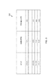
[0039]一実施形態による、例となるルックアップ表が図4に例示される。図4では、ルックアップ表365は、ミリボルト単位のステップサイズの選択を提供する、左側の列を含む。右側の列は、1秒当たりの摂氏度単位のランプレート測定値を提供する。これら列の各々は、測定されたランプレートに特定のサイズの電圧ステップを割り当てる。例えば、エントリ410は、測定された1秒当たり25℃のランプレートに、15mVのステップサイズを割り当てる。同様に、エントリ440は、1秒当たり55℃の測定されたランプレートに、65mVのステップサイズを割り当てる。他のエントリ420、430は、それぞれ、上限(top end)のエントリ440と下限(bottom end)のエントリ410の間の中間である。無論、図4に例示される表365は、一例である。他の実施形態は、特定のアプリケーションに適切なより多くのまたはより少ないエントリ、異なるステップサイズ、および異なるランプレートを含み得ることが理解される。
An example lookup table according to one embodiment is illustrated in FIG. In FIG. 4, the look-up table 365 includes a left column that provides a selection of step sizes in millivolts. The right column provides rampette measurements in degrees Celsius per second. Each of these columns assigns a voltage step of a particular size to the measured rampette. For example,
[0040]図5は、一実施形態による、例となるランプレートを例示する。ランプレートは、ベンチマークテストの持続時間のような、定義された時間期間にわたる温度変化を含む。曲線510は、より望ましくない熱伝導特性を有するよりローエンドのコンピューティングデバイスに関連付けられ得る、例となるランプレートを例示する。曲線510の例では、コンピューティングデバイスの伝導特性は、ジャンクション温度または計算されたTskinが比較的迅速に上昇することを可能にする。対照的に、曲線520は、より望ましい熱伝導特性を有するよりハイエンドのコンピューティングデバイスに関連付けられ得る、例となるランプレートを例示する。曲線520において、ジャンクション温度および/またはスキン温度の上昇は、それほど迅速ではない。この例では、より高いジャンクション温度ランプレートまたはTskinランプレートが、許容レベルに温度を制御するために、より大きい電圧ステップに関連付けられるであろう。したがって、曲線510は、曲線520(15mV)よりも大きい電圧ステップ(35mV)に関連付けられる。これは、より高い温度ランプレートが、より大きい電圧ステップに関連付けられた、図4の例となるルックアップ表365と一致する。
[0040] FIG. 5 illustrates an exemplary lamp plate according to one embodiment. Lamplate includes temperature changes over a defined time period, such as the duration of a benchmark test.
[0041]図3の例に戻ると、アクション360において、コンピュータプロセッサは、アクション340からTJランプレート測定値を受け取り、その後、TJランプレート測定値をルックアップ表365中のエントリと比較する。アクション360は、切り上げまたは切り捨て、最も近いマッチを見つけること、または別の選択基準を使用することによるものを含む、TJランプレートの測定された値と、表365中の利用可能なエントリとの間の近似マッチングを行うことを含む。したがって、アクション360は、観測されたTJランプレートを、表中のTJランプレート値にマッチングするために、データ構造(このケースでは、表365)を解析することと、表中のTJランプレート値に対応する電圧ステップ値を選択することと、その後、DCVSアルゴリズムに電圧ステップ値を適用することとを含む。無論、他の実施形態は、ジャンクション温度を使用することに加えて、またはその代替として、観測されたTskinランプレートを表中のエントリとマッチングし、対応する電圧ステップサイズを適用し得る。換言すれば、他の実施形態においてTskinに基づいて電圧低減ステップサイズを設定することは、ジャンクション温度を使用するアクション360と同様に機能する。
[0041] Returning to the example of FIG. 3, at
[0042]図6は、一実施形態による、通常動作中のDCVSビヘイビア(DCVS behavior)の例示である。具体的には、アクション360は、較正中にルックアップ表365から適切な電圧ステップサイズを選択および適用することを含み得、その後、通常動作中に、DCVSアルゴリズムは、それが適用された電圧ステップサイズを使用するに伴って、図6に例示されるものと同様のビヘイビアを示す。
[0042] FIG. 6 is an example of a DCVS behavior during normal operation according to one embodiment. Specifically,
[0043]図6は、3つの列を有する表600を示し、ここにおいて、右側の列は、50mVの電圧ステップを例示する。具体的には、ステップ1とステップ2の間の差が50mVであり、また、ステップ2とステップ3の間にも50mV電圧差分(voltage delta)が存在する。ステップ3とステップnの間のステップは、図6のビヘイビアが任意の数のステップを含み得ることを示すために、具体的には例示されていない。ステップnは、650mVに関連付けられているが、ビヘイビアの上限および下限は、様々な実施形態において、任意の適切な電圧レベルに設定され得ることが理解される。
[0043] FIG. 6 shows Table 600 with three columns, where the right column illustrates a voltage step of 50 mV. Specifically, the difference between step 1 and
[0044]真ん中の列は、それぞれの電圧レベルおよびステップに関連付けられた周波数値を示す。一般に、より低い電圧での動作は、データビットが適正に捕捉されることを確実にするために、より低いクロック周波数での動作に関連付けられていることが予期される。したがって、図6の実施形態は、より低い動作周波数をより低い動作電圧と関連付ける。様々な実施形態は、適宜、電圧およびクロック周波数を上昇および低下させ得る。 The middle column shows the frequency values associated with each voltage level and step. In general, operation at lower voltages is expected to be associated with operation at lower clock frequencies to ensure that the data bits are properly captured. Therefore, the embodiment of FIG. 6 associates a lower operating frequency with a lower operating voltage. Various embodiments may increase and decrease the voltage and clock frequency as appropriate.
[0045]例えば、図6の行の各々は、温度緩和アルゴリズムによって取られるアクションに対応し得る。したがって、一例では、最初の温度セットポイント(TJまたはTskin)が、上昇する温度読取り値によって超えられたとき、温度緩和アルゴリズムは、ステップ1に進み、モニタすることを継続し得る。温度が、特定の時間期間よりも長い間、同じ状態のままであるか、または増大し続けた場合には、温度緩和アルゴリズムは、ステップ2に移動してモニタすることを継続し、温度が安定化したか、または低減し始めた後に、電圧をさらに低減させ続けるか、あるいは電圧を増大し始めるかのいずれかである(either continuing to further decrease the voltage or to begin increasing the voltage after temperature stabilizes or begins to decrease)。 [0045] For example, each of the rows in FIG. 6 may correspond to an action taken by a temperature relaxation algorithm. Thus, in one example, when the first temperature setpoint ( TJ or Tskin) is exceeded by the rising temperature reading, the temperature relaxation algorithm may proceed to step 1 and continue to monitor. If the temperature remains the same or continues to increase for longer than a certain time period, the temperature relaxation algorithm continues to move to step 2 to monitor and the temperature stabilizes. Either continuing to further decrease the voltage or to begin increasing the voltage after temperature stabilizes or begins. to decrease).
[0046]アクション360はまた、性能評価尺度(performance measure)または緩和までの時間に基づいて、電圧ステップサイズを選択することも含み得、ここにおいて、緩和までのより短い時間は、より大きい電圧ステップに関連付けられ得、ここにおいて、より高い測定された性能は、より大きい電圧ステップに関連付けられ得る。
[0046]
[0047]アクション370は、TJランプレート(アクション340)および緩和までの時間(アクション330)に少なくとも部分的に基づいて、温度セットポイントおよびシャットダウンポイントを更新することを含む。セットポイントは、DCVSのような、緩和アルゴリズムが呼び出され得る、様々な温度センサでの温度読取り値を含む。一般に、より短い緩和までの時間およびより大きいランプレートは、より低い温度セットポイントをもたらすことになる。アクション370は、コンピュータプロセッサが、アクション330、340からの値を受け取り、それらの値をルックアップ表375にマッチングするという点では、アクション360と同様であり得る。その後、アクション370は、温度セットポイントとして、ルックアップ表からのエントリを適用する。
[0047]
[0048]アクション370は、シャットダウンポイントを更新することをさらに含み得る。この例では、シャットダウンポイントは、集積回路チップが熱暴走イベントを回避するために完全にオフにされ得る、温度読取り値を含む。一般に、より短い緩和までの時間およびより大きいランプレートは、より低いシャットダウンポイントをもたらすことになる。アクション370は、コンピュータプロセッサが、アクション330、340からの値を受け取り、それらの値をルックアップ表375内でマッチングして、適切なシャットダウンポイントを識別し、温度緩和アルゴリズムにそれらのシャットダウンポイントを適用することを含む。
[0048]
[0049]アクション390は、アクション350からの測定されたTskinランプレートに応答して、スキン温度セットポイントを更新することを含む。アクション390は、コンピュータプロセッサが、アクション350からの値を受け取ることと、それらの値をルックアップ表395中のエントリにマッチングすることを含む。その後、アクション390は、緩和アルゴリズムにおけるスキン温度セットポイントとして、ルックアップ表395から選択されたエントリを適用する。スキン温度セットポイントは、Tskin推定値に対応する温度値を含み得る。コンピュータデバイスが、通常動作中に動作するにつれて、それはまた、Tskinを計算し得、Tskinがセットポイントを超えるとき、温度緩和は、上記で説明されたように、動作電圧および/または動作周波数を低減させることによって実行され得る。
[0049]
[0050]アクション380は、TJランプレート測定値を受け取ることと、適切なポーリングレート値を識別するために、それらの測定値をルックアップ表385中の値にマッチングすることとを含む。この例では、ポーリングレートは、温度センサから温度データを獲得するための頻度(frequency)を含む。一般に、より大きいジャンクション温度ランプレートは、温度センサについてのより高いポーリングレートに対応すべきであると仮定される。アクション380は、適切なポーリングレートを識別するために、測定されたTJランプレート情報を使用することと、温度緩和アルゴリズムにそれらのポーリングレートを適用することとを含む。
[0050]
[0051]実施形態は、特定のスマートフォンまたは他のコンピューティングデバイスの製造プロセス中に方法300を実行することを含み得る。これは、特定のデバイスの熱ポリシ(thermal policies)が、そのデバイスに対して個別に設定されることを可能にする。その後、方法300は、熱ポリシを調整するために、年に1回またはその他のときなどに、適宜、再実行され得る。対照的に、様々な従来のプロセスは、その特定のモデルの各デバイスが同じ熱ポリシを含むように、デバイスモデルに対して熱ポリシを設定することを含む。 [0051] Embodiments may include performing method 300 during the manufacturing process of a particular smartphone or other computing device. This allows the thermal policies of a particular device to be set individually for that device. The method 300 can then be re-executed as appropriate, such as once a year or at other times, to adjust the thermal policy. In contrast, various conventional processes involve setting a thermal policy for a device model so that each device of that particular model contains the same thermal policy.
[0052]温度緩和アルゴリズムを較正するために方法300を使用するいくつかの実施形態の利点は、それらの実施形態が、所与の製造されたコンピューティングデバイスに特有の設定を適用し得るということである。例えば、所与の製造されたコンピューティングデバイスは、チップパッケージとヒートスプレッダとの間のエアギャップのような、製造ばらつきを有し得、これは、コンピューティングデバイスの熱伝導特性に影響を及ぼす。方法300は、ベンチマークテストを実行し、その後、較正を実行して、その製造されたコンピューティングデバイスについての適切な設定を識別する。同じ設備で製造された他のコンピューティングデバイスは、同じ型番を使用していてさえも、製造ばらつきによる異なる熱伝導特性を有し得、したがって、それらの個々のデバイスにとってより好ましい幾分か異なる温度緩和設定を含み得る。 [0052] The advantage of some embodiments using Method 300 to calibrate the temperature relaxation algorithm is that those embodiments may apply settings specific to a given manufactured computing device. Is. For example, a given manufactured computing device can have manufacturing variability, such as an air gap between a chip package and a heat spreader, which affects the thermal conductivity of the computing device. Method 300 performs a benchmark test and then performs calibration to identify the appropriate settings for the manufactured computing device. Other computing devices manufactured in the same equipment can have different thermal conductivity characteristics due to manufacturing variability, even using the same model number, and therefore somewhat different temperatures that are more preferred for those individual devices. May include mitigation settings.
[0053]熱緩和を提供する例となる方法700のフロー図が、図7に例示される。一例では、方法700は、熱管理ユニットによって実行され、これは、コンピューティングデバイスのプロセッサにおけるハードウェアおよび/またはソフトウェア機能を含み得る。いくつかの例では、熱管理ユニットは、コンピューティングデバイスにおける温度センサから温度データを受け取ることと、特定のアルゴリズムに従って、較正機能および温度緩和機能を実行することとを行うためのコンピュータ可読命令を実行する処理回路を含む。
[0053] A flow diagram of
[0054]図7の実施形態は、較正動作中に、アクション710〜740を実行することを含む。例えば、アクション710〜740は、コンピューティングベンチマークテストを実行することと、そのコンピューティングベンチマークテスト中に値を捕捉することとに応答して実行され得る。アクション750は、較正された温度緩和アルゴリズムを使用して、通常動作中に実行され得る。
[0054] The embodiment of FIG. 7 includes performing actions 710-740 during the calibration operation. For example, actions 710-740 may be performed in response to performing a computing benchmark test and capturing values during that computing benchmark test.
[0055]アクション710において、熱管理ユニットは、集積回路チップにおける温度センサおよびプリント回路基板上の温度センサから温度感知データを読み取る。例が、図2において上記に示され、ここで、温度センサは、TJ1〜TJ3として示されている。この例でのアクション710は、コンピューティングベンチマークテスト中に、デフォルトのレートで温度センサをポーリングすることを含み得る。アクション710はまた、図3のアクション320〜350に関して上記で説明されたように、性能を測定することと、デフォルトの温度緩和設定を使用して、緩和までの時間を測定することと、TJランプレートを測定することと、Tskinランプレートを測定することとを含み得る。
[0055] In
[0056]アクション720において、熱管理ユニットは、温度情報の観測された変化速度を、データ構造中の特定の温度情報変化速度値にマッチングするために、データ構造を解析する。例えば、上記の例では、温度情報の変化速度は、ランプレートを含む。さらに、上記の例では、熱管理ユニットは、近似的にマッチするランプレート値(approximately matching ramp rate value)に対応する表中のエントリを見つけるためのキーとして、TJランプレート(またはTskinランプレート)を使用して、ルックアップ表を調べる。換言すれば、ランプレートは、表中のエントリを選択するために、キーと値のペアにおけるキーとして使用され得る。上記例は、データ構造としてルックアップ表を使用するが、実施形態の範囲は、そのように限定されない。他の実施形態は、適宜、異なるデータ構造を使用し得る。
[0056] In
[0057]アクション730において、熱管理ユニットは、データ構造中の特定の温度情報変化速度値に対応する第1の電圧低減ステップ値を選択する。一例が図4に関して上記に提供され、ここにおいて、左側の列における電圧低減ステップ値の各々は、右側の列におけるそれぞれのランプレート値に対応する。アクション730、熱管理ユニットは、アクション720の解析することに応答して、電圧低減ステップ値を選択する。
[0057] In
[0058]アクション740において、熱管理ユニットは、温度緩和アルゴリズムに第1の電圧低減ステップ値を適用する。例えば、熱管理ユニットは、コンピューティングデバイスのチップにおける不揮発性メモリ中に第1の電圧低減ステップ値のインジケーションを記憶し得る。
[0058] In
[0059]アクション750において、熱緩和ユニットは、コンピューティングデバイスの通常動作中に、温度緩和アルゴリズムに従って、コンピューティングデバイスの性能を低減させる。一例では、温度緩和アルゴリズムは、較正からの設定を収集するために、コンピュータチップ内の不揮発性メモリアドレスを読み取ることによって、デバイスの電源投入時に自分自身を始動するソフトウェアアルゴリズムである。それらの設定のうちの1つが、第1の電圧低減ステップ値である。他の設定は、同様に不揮発性メモリアドレスに記憶された、例えば、TJセットポイントおよびシャットダウンポイント、Tskinセットポイント、温度センサポーリングレート、および同様のものを含み得る。
[0059] In
[0060]アクション750は、コンピューティングデバイスの少なくとも1つの集積回路チップによって消費されるエネルギを低減させることを含む。一例では、温度緩和アルゴリズムは、1つまたは複数の集積回路チップの動作電圧を低減させ、それによって、電力消費を低減させる。しかしながら、実施形態の範囲は、電圧低減の一部としてか、あるいは電圧低減とは独立してかにかかわらず、動作周波数を低減させるなど、任意の適切な温度緩和技法を含み得る。
[0060]
[0061]通常の使用中にデバイスが動作するにつれて、熱管理ユニットは、バックグラウンドにおいて温度緩和アルゴリズムを実行し、増大している温度読取り値または低減している温度読取り値のいずれかにおいて、ジャンクション温度セットポイントおよびスキン温度セットポイントが通過されると(passed)、適切なアクションを取る。したがって、人間のユーザが、デバイスをアイドル状態にしておく、電話をかける、テキストメッセージを送る、ビデオを見る、および同様のことを行うとき、熱管理ユニットは、デバイス動作温度がスキンの限界を超えないことを確実にするために、較正された温度緩和アルゴリズムを連続的に実行する。 [0061] As the device operates during normal use, the thermal management unit runs a temperature mitigation algorithm in the background and junctions in either an increasing or decreasing temperature reading. When the temperature setpoint and skin temperature setpoint are passed (passed), take appropriate action. Therefore, when a human user keeps the device idle, makes a phone call, sends a text message, watches a video, and does the same, the thermal management unit causes the device operating temperature to exceed the skin limit. A calibrated temperature relaxation algorithm is run continuously to ensure that it is not.
[0062]実施形態の範囲は、図7に示された特定の方法に限定されない。他の実施形態は、1つまたは複数のアクションを追加、省略、再配置、または修正し得る。例えば、方法700は、アクション710〜740が繰り返されるか否かにかかわらず、通常動作中にアクション750を繰り返し実行することを含み得る。
[0062] The scope of the embodiments is not limited to the particular method shown in FIG. Other embodiments may add, omit, rearrange, or modify one or more actions. For example,
[0063]現時点で当業者が認識するように、および目前の特定のアプリケーションに依存して、多くの修正、置換および変形が、その趣旨および範囲から逸脱することなく、本開示のデバイスの材料、装置、構成、および使用方法において、ならびにそれらに対してなされ得る。この点を踏まえると、本開示の範囲は、ここに例示および説明された特定の実施形態のそれに限定されるべきではなく、これは、それらが単にそれについてのいくつかの例にすぎないためであり、むしろ、以下に添付された特許請求の範囲およびそれらの機能的な同等物のそれに完全に相応すべきである。
以下に本願発明の当初の特許請求の範囲に記載された発明を付記する。
[C1]
コンピューティングデバイス内の複数の温度センサから温度情報を生成することと、 前記温度情報の観測された変化速度に基づいて、電圧低減ステップを生成するために、前記温度情報を処理することと
を備える方法。
[C2]
前記コンピューティングデバイスの通常動作中、および前記コンピューティングデバイスの通常動作中に受け取られた更なる温度情報に応答して、前記コンピューティングデバイスの性能を低下させること
をさらに備える、C1に記載の方法。
[C3]
前記コンピューティングデバイスの前記性能を低下させることは、前記コンピューティングデバイスの動作の電圧を低減させることに加えて、前記コンピューティングデバイスの動作の周波数を低減させることを備える、C2に記載の方法。
[C4]
前記コンピューティングデバイスの前記性能を低下させることは、前記温度緩和アルゴリズムにおける前記電圧低減ステップに従って、前記コンピューティングデバイスの動作電圧を低減させることを備える、C2に記載の方法。
[C5]
前記電圧低減ステップは、それぞれの周波数低減ステップに関連付けられている、C1に記載の方法。
[C6]
前記温度情報の前記観測された変化速度は、
前記コンピューティングデバイスのジャンクション温度に関連付けられた温度情報の変化速度
を備える、C1に記載の方法。
[C7]
前記コンピューティングデバイスの前記ジャンクション温度は、前記デバイスの複数の温度センサのうちの第1の温度センサの読取り値を備え、ここにおいて、前記読取り値は、前記複数の温度センサのうちの最も高い読取り値である、C6に記載の方法。
[C8]
データ構造中に電圧差分として複数の電圧低減ステップ値を記憶すること、各電圧低減ステップ値は、周波数低減ステップ値および温度情報変化速度値に関連付けられている、 をさらに備える、C1に記載の方法。
[C9]
前記データ構造は、ルックアップ表を備える、C8に記載の方法。
[C10]
前記温度情報を処理することは、
前記温度情報の前記観測された変化速度を、前記データ構造中の特定の温度情報変化速度値にマッチングするために、前記データ構造を解析することと、
前記データ構造中の前記特定の温度情報変化速度値に対応する第1の電圧低減ステップ値を選択することと、
前記第1の電圧低減ステップ値分だけ前記コンピューティングデバイスの動作電圧を低減させることと
を備える、C8に記載の方法。
[C11]
前記コンピューティングデバイスの通常動作中に前記第1の電圧低減ステップ値を使用すること
をさらに備える、C10に記載の方法。
[C12]
コンピュータ可読命令を実行するように構成されたコンピュータプロセッサと、前記コンピュータプロセッサは、コンピューティングデバイス中に取り付けられており、
前記コンピューティングデバイス内に配置された温度感知デバイスと、前記温度感知デバイスは、前記コンピュータプロセッサと通信するように構成され、前記コンピュータプロセッサは、以下の動作を実行するように構成される:
前記温度感知デバイスから温度情報を受け取ること、
前記温度情報からジャンクション温度ランプレート値を計算すること、および
前記ジャンクション温度ランプレート値に基づいて、電圧低減ステップを設定すること、
を備えるシステム。
[C13]
前記温度感知デバイスは、前記コンピューティングデバイスのプリント回路基板上に配置され、前記プリント回路基板は、前記コンピューティングデバイスのハウジング内に封入される、C12に記載のシステム。
[C14]
前記温度感知デバイスは、前記コンピューティングデバイスのハウジング内に封入された複数の温度感知デバイスのうちの1つである、C12に記載のシステム。
[C15]
前記デバイスのジャンクション温度が、前記複数の温度感知デバイスのうちの前記温度センサの読取り値を備え、前記読取り値は、前記複数の温度感知デバイスのうちの最も高い読取り値である、C14に記載のシステム。
[C16]
前記ジャンクション温度ランプレート値は、前記コンピューティングデバイスの較正動作中のジャンクション温度の変化速度を備える、C12に記載のシステム。
[C17]
前記コンピュータプロセッサは、通常動作中、前記電圧低減ステップに従って、前記コンピュータプロセッサの動作電圧を低減させるようにさらに構成される、C12に記載のシステム。
[C18]
コンピューティングデバイスの外部ハウジング内の複数の位置において温度を感知するための手段と、
前記温度を感知する手段からの温度データからジャンクション温度ランプレートを計算するための手段と、
前記ジャンクション温度ランプレートに基づいて、電圧低減ステップサイズ値を選択するために、ルックアップ表を解析するための手段と、
前記電圧低減ステップサイズ値分だけ動作電圧を低減させるための手段と
を備えるコンピューティングデバイス。
[C19]
前記ジャンクション温度ランプレートを計算するための前記手段は、
複数の温度センサを備え、ここにおいて、前記複数の温度センサの第1のサブセットが、前記コンピューティングデバイスの半導体チップ内に配置され、ここにおいて、前記複数の温度センサの第2のサブセットが、前記コンピューティングデバイスのプリント回路基板上に配置される、
C18に記載のコンピューティングデバイス。
[C20]
前記コンピューティングデバイスの不揮発性メモリ中に前記電圧低減ステップサイズ値を記憶するための手段
をさらに備える、C18に記載のコンピューティングデバイス。
[C21]
前記不揮発性メモリから、前記電圧低減ステップサイズ値を取り出すための手段
をさらに備える、C20に記載のコンピューティングデバイス。
[C22]
前記ジャンクション温度ランプレートを計算するための前記手段は、
前記温度を感知する手段の中で最も高い温度読取り値を決定するために、前記温度を感知する手段をポーリングするための手段と、
前記温度を感知する手段の中で前記最も高い温度読取り値から前記ジャンクション温度ランプレートを生成するための手段と
を備える、C18に記載のコンピューティングデバイス。
[C23]
第1の時間期間の間、コンピューティングデバイスのハウジングの内部にある複数の温度センサから温度データを収集することと、
前記温度データから前記コンピューティングデバイスの温度ランプレートを測定することと、
データ構造から値を選択するためのキーとして、前記温度ランプレートを使用することと、ここにおいて、前記値は、電圧ステップサイズを含み、
前記電圧ステップサイズ分だけ前記コンピューティングデバイスの動作電圧を低減させることと
を備える方法。
[C24]
温度データを収集することは、
温度データが収集されるにつれて、前記複数の温度センサの最高の温度読取り値として、ジャンクション温度を計算すること
をさらに備え、
ここにおいて、前記温度ランプレートを測定することは、前記ジャンクション温度のランプレートを測定することを備える、
C23に記載の方法。
[C25]
前記温度ランプレートを測定することは、
前記コンピューティングデバイスのスキン温度を計算することと、
前記コンピューティングデバイスの前記スキン温度のランプレートを計算することと を備える、C23に記載の方法。
[C26]
前記電圧ステップサイズは、電圧差分を備える、C23に記載の方法。
[C27]
前記電圧ステップサイズを適用することは、
前記測定された温度ランプレートを、前記データ構造中のランプレート値にマッチングするために、前記データ構造を解析することと、
前記データ構造中の前記ランプレート値に対応する前記電圧ステップサイズを選択することと、
前記コンピューティングデバイスにおけるデータ記憶デバイスにおいて、前記電圧ステップサイズを記憶することと
を備える、C23に記載の方法。
[0063] As will be recognized by those skilled in the art at this time, and depending on the particular application at hand, many modifications, substitutions and modifications, without departing from their intent and scope, the materials of the devices of the present disclosure. It can be done in the equipment, configuration, and usage, and for them. In this regard, the scope of the present disclosure should not be limited to that of the particular embodiments exemplified and described herein, as they are merely some examples of it. Yes, rather, it should be in full agreement with the claims and their functional equivalents attached below.
The inventions described in the original claims of the present invention are described below.
[C1]
Generating temperature information from multiple temperature sensors in a computing device and processing the temperature information to generate a voltage reduction step based on the observed rate of change of the temperature information.
How to prepare.
[C2]
Degrading the performance of the computing device in response to additional temperature information received during normal operation of the computing device and during normal operation of the computing device.
The method according to C1, further comprising.
[C3]
The method according to C2, wherein reducing the performance of the computing device comprises reducing the operating frequency of the computing device in addition to reducing the operating voltage of the computing device.
[C4]
The method according to C2, wherein reducing the performance of the computing device comprises reducing the operating voltage of the computing device according to the voltage reduction step in the temperature relaxation algorithm.
[C5]
The method of C1, wherein the voltage reduction steps are associated with each frequency reduction step.
[C6]
The observed rate of change of the temperature information is
The rate of change of temperature information associated with the junction temperature of the computing device
The method according to C1.
[C7]
The junction temperature of the computing device comprises a reading of a first temperature sensor of the plurality of temperature sensors of the device, wherein the reading is the highest reading of the plurality of temperature sensors. The method according to C6, which is a value.
[C8]
The method according to C1, further comprising storing a plurality of voltage reduction step values as voltage differences in the data structure, each voltage reduction step value being associated with a frequency reduction step value and a temperature information change rate value. ..
[C9]
The method of C8, wherein the data structure comprises a look-up table.
[C10]
Processing the temperature information
Analyzing the data structure to match the observed rate of change of the temperature information with a specific rate of change in temperature information in the data structure.
Selecting the first voltage reduction step value corresponding to the particular temperature information change rate value in the data structure, and
To reduce the operating voltage of the computing device by the value of the first voltage reduction step.
The method according to C8.
[C11]
Using the first voltage reduction step value during normal operation of the computing device.
The method according to C10, further comprising.
[C12]
A computer processor configured to execute computer-readable instructions and said computer processor are mounted in a computing device.
A temperature-sensing device located within the computing device and the temperature-sensing device are configured to communicate with the computer processor, which is configured to perform the following operations:
Receiving temperature information from the temperature sensing device,
Calculate the junction temperature ramp rate value from the temperature information, and
Setting the voltage reduction step based on the junction temperature ramp plate value,
System with.
[C13]
The system according to C12, wherein the temperature sensing device is arranged on a printed circuit board of the computing device, and the printed circuit board is enclosed in a housing of the computing device.
[C14]
The system according to C12, wherein the temperature sensing device is one of a plurality of temperature sensing devices encapsulated within the housing of the computing device.
[C15]
C14, wherein the junction temperature of the device comprises a reading of the temperature sensor among the plurality of temperature sensing devices, the reading being the highest reading of the plurality of temperature sensing devices. system.
[C16]
The system according to C12, wherein the junction temperature ramp rate value comprises the rate of change of the junction temperature during the calibration operation of the computing device.
[C17]
The system according to C12, wherein the computer processor is further configured to reduce the operating voltage of the computer processor according to the voltage reduction step during normal operation.
[C18]
A means for sensing temperature at multiple locations within the outer housing of a computing device,
A means for calculating the junction temperature ramp rate from the temperature data from the means for sensing the temperature, and
A means for analyzing a look-up table to select a voltage reduction step size value based on the junction temperature ramp plate, and
As a means for reducing the operating voltage by the voltage reduction step size value
Computing device with.
[C19]
The means for calculating the junction temperature rampette is
It comprises a plurality of temperature sensors, wherein a first subset of the plurality of temperature sensors is located within a semiconductor chip of the computing device, wherein a second subset of the plurality of temperature sensors is said. Placed on the printed circuit board of a computing device,
The computing device according to C18.
[C20]
Means for storing the voltage reduction step size value in the non-volatile memory of the computing device
The computing device according to C18.
[C21]
Means for extracting the voltage reduction step size value from the non-volatile memory
The computing device according to C20, further comprising.
[C22]
The means for calculating the junction temperature rampette is
A means for polling the means for sensing the temperature and a means for polling the means for sensing the temperature in order to determine the highest temperature reading of the means for sensing the temperature.
As a means for generating the junction temperature ramplate from the highest temperature reading among the means for sensing the temperature.
The computing device according to C18.
[C23]
Collecting temperature data from multiple temperature sensors inside the housing of the computing device during the first time period,
Measuring the temperature ramp rate of the computing device from the temperature data,
Using the temperature rampator as a key for selecting a value from a data structure, wherein the value includes a voltage step size.
To reduce the operating voltage of the computing device by the voltage step size.
How to prepare.
[C24]
Collecting temperature data is
As temperature data is collected, calculate the junction temperature as the best temperature reading of the multiple temperature sensors.
With more
Here, measuring the temperature lamp plate includes measuring the lamp plate at the junction temperature.
The method according to C23.
[C25]
Measuring the temperature lamp plate
Calculating the skin temperature of the computing device
23. The method of C23, comprising calculating the ramp rate of the skin temperature of the computing device.
[C26]
The method according to C23, wherein the voltage step size comprises a voltage difference.
[C27]
Applying the voltage step size
Analyzing the data structure to match the measured temperature lamp plate to the ramp plate value in the data structure.
Selecting the voltage step size corresponding to the ramp rate value in the data structure and
In the data storage device in the computing device, storing the voltage step size
The method according to C23.
Claims (14)
コンピューティングデバイス内の複数の温度センサから温度情報を生成することと、
前記温度情報の観測された変化速度に基づいて、電圧低減ステップを生成するために、前記温度情報を処理することと、
データ構造中に電圧差分として複数の電圧低減ステップ値を記憶すること、各電圧低減ステップ値は、周波数低減ステップ値および温度情報変化速度値に関連付けられている、ここにおいて、前記データ構造は、ルックアップ表を備える、
を備える、方法。 It is a method performed by a computer, and the above method is
Generating temperature information from multiple temperature sensors in a computing device,
Processing the temperature information to generate a voltage reduction step based on the observed rate of change of the temperature information .
Store multiple voltage reduction step values as voltage differences in the data structure, each voltage reduction step value is associated with a frequency reduction step value and a temperature information change rate value, where the data structure looks. With a close-up table,
Equipped with a, way.
をさらに備える、請求項1に記載の方法。 The first aspect of claim 1, further comprising degrading the performance of the computing device in response to further temperature information received during normal operation of the computing device and during normal operation of the computing device. the method of.
前記コンピューティングデバイスのジャンクション温度に関連付けられた温度情報の変化速度
を備える、請求項1に記載の方法。 The observed rate of change of the temperature information is
The method of claim 1, comprising the rate of change of temperature information associated with the junction temperature of the computing device.
前記温度情報の前記観測された変化速度を、前記データ構造中の特定の温度情報変化速度値にマッチングするために、前記データ構造を解析することと、
前記データ構造中の前記特定の温度情報変化速度値に対応する第1の電圧低減ステップ値を選択することと、
前記第1の電圧低減ステップ値分だけ前記コンピューティングデバイスの動作電圧を低減させることと
を備える、請求項1に記載の方法。 Processing the temperature information
Analyzing the data structure to match the observed rate of change of the temperature information with a specific rate of change in temperature information in the data structure.
Selecting the first voltage reduction step value corresponding to the particular temperature information change rate value in the data structure, and
And a reducing the operating voltage of the first voltage reduction step value amount corresponding the computing device, the method according to claim 1.
をさらに備える、請求項7に記載の方法。 The method of claim 7 , further comprising using the first voltage reduction step value during normal operation of the computing device.
前記コンピューティングデバイス内に配置された温度感知デバイスと、前記温度感知デバイスは、前記コンピュータプロセッサと通信するように構成され、前記コンピュータプロセッサは、以下の動作を実行するように構成される:
前記温度感知デバイスから温度情報を受け取ることと、
前記温度情報からジャンクション温度ランプレート値を計算することと、
前記ジャンクション温度ランプレート値に基づいて、電圧低減ステップを設定することと、
データ構造中に電圧差分として複数の電圧低減ステップ値を記憶すること、各電圧低減ステップ値は、周波数低減ステップ値および温度情報変化速度値に関連付けられている、ここにおいて、前記データ構造は、ルックアップ表を備える、
を備えるシステム。 A computer processor configured to execute computer-readable instructions and said computer processor are mounted in a computing device.
A temperature-sensing device located within the computing device and the temperature-sensing device are configured to communicate with the computer processor, which is configured to perform the following operations:
And receiving temperature information from the temperature sensing device,
Calculating a junction temperature ramp value from the temperature information,
On the basis of the junction temperature ramp value, and setting the voltage reduction step,
Store multiple voltage reduction step values as voltage differences in the data structure, each voltage reduction step value is associated with a frequency reduction step value and a temperature information change rate value, where the data structure looks. With a close-up table,
System with.
Applications Claiming Priority (3)
| Application Number | Priority Date | Filing Date | Title |
|---|---|---|---|
| US15/205,678 US10007310B2 (en) | 2016-07-08 | 2016-07-08 | Circuits and methods providing calibration for temperature mitigation in a computing device |
| US15/205,678 | 2016-07-08 | ||
| PCT/US2017/037502 WO2018009317A1 (en) | 2016-07-08 | 2017-06-14 | Circuits and methods providing calibration for temperature mitigation in a computing device |
Publications (3)
| Publication Number | Publication Date |
|---|---|
| JP2019527412A JP2019527412A (en) | 2019-09-26 |
| JP2019527412A5 JP2019527412A5 (en) | 2020-06-25 |
| JP6926185B2 true JP6926185B2 (en) | 2021-08-25 |
Family
ID=59216051
Family Applications (1)
| Application Number | Title | Priority Date | Filing Date |
|---|---|---|---|
| JP2019500296A Active JP6926185B2 (en) | 2016-07-08 | 2017-06-14 | Circuits and methods that provide calibration for temperature relaxation in computing devices |
Country Status (9)
| Country | Link |
|---|---|
| US (1) | US10007310B2 (en) |
| EP (1) | EP3482274B1 (en) |
| JP (1) | JP6926185B2 (en) |
| KR (1) | KR102513430B1 (en) |
| CN (2) | CN109416568B (en) |
| BR (1) | BR112019000012A8 (en) |
| ES (1) | ES2770108T3 (en) |
| HU (1) | HUE047310T2 (en) |
| WO (1) | WO2018009317A1 (en) |
Families Citing this family (6)
| Publication number | Priority date | Publication date | Assignee | Title |
|---|---|---|---|---|
| US11399720B2 (en) | 2016-04-05 | 2022-08-02 | Qulacomm Incorporated | Circuits and methods providing temperature mitigation for computing devices |
| US10402205B2 (en) * | 2017-03-02 | 2019-09-03 | Quanta Computer Inc. | System and method for dynamically optimizing hardware frequency for booting |
| KR102400977B1 (en) * | 2020-05-29 | 2022-05-25 | 성균관대학교산학협력단 | Method for processing page fault by a processor |
| CN111966409B (en) * | 2020-07-30 | 2021-04-02 | 深圳比特微电子科技有限公司 | Quick frequency searching method and device for mining machine and mining machine |
| CN112462820B (en) * | 2020-10-29 | 2022-03-22 | 广东禅信通科技有限公司 | Temperature control system and method for graphene heating material and storage medium |
| KR102679433B1 (en) * | 2020-11-25 | 2024-06-28 | (주)하이페리온테크 | Apparatus and method for processing sensor data based on adaptive polling |
Family Cites Families (20)
| Publication number | Priority date | Publication date | Assignee | Title |
|---|---|---|---|---|
| US5940785A (en) * | 1996-04-29 | 1999-08-17 | International Business Machines Corporation | Performance-temperature optimization by cooperatively varying the voltage and frequency of a circuit |
| US20020087904A1 (en) * | 2000-12-28 | 2002-07-04 | Zhong-Ning (George) Cai | Method and apparatus for thermal sensitivity based dynamic power control |
| US6977646B1 (en) * | 2001-11-30 | 2005-12-20 | 3M Innovative Properties Co. | Touch screen calibration system and method |
| KR20050085690A (en) * | 2002-12-17 | 2005-08-29 | 코닌클리즈케 필립스 일렉트로닉스 엔.브이. | Temperature compensated r-c oscillator |
| WO2004104778A2 (en) | 2003-05-19 | 2004-12-02 | Modular Computing & Communications Corporation | Apparatus and method for mobile personal computing and communications |
| US7461272B2 (en) | 2004-12-21 | 2008-12-02 | Intel Corporation | Device, system and method of thermal control |
| US7535020B2 (en) * | 2005-06-28 | 2009-05-19 | Kabushiki Kaisha Toshiba | Systems and methods for thermal sensing |
| US7900069B2 (en) * | 2007-03-29 | 2011-03-01 | Intel Corporation | Dynamic power reduction |
| US8315746B2 (en) * | 2008-05-30 | 2012-11-20 | Apple Inc. | Thermal management techniques in an electronic device |
| US8402290B2 (en) * | 2008-10-31 | 2013-03-19 | Intel Corporation | Power management for multiple processor cores |
| US8996330B2 (en) * | 2011-01-06 | 2015-03-31 | Qualcomm Incorporated | Method and system for managing thermal policies of a portable computing device |
| US8760217B2 (en) * | 2011-02-25 | 2014-06-24 | Qualcomm Incorporated | Semiconductor device having on-chip voltage regulator |
| KR101840852B1 (en) | 2011-10-10 | 2018-03-22 | 삼성전자주식회사 | Surface temperature management method of mobile device and memory thermal management method of multichip package |
| US9703336B2 (en) | 2013-02-21 | 2017-07-11 | Qualcomm Incorporated | System and method for thermal management in a multi-functional portable computing device |
| US9529397B2 (en) | 2013-03-01 | 2016-12-27 | Qualcomm Incorporated | Thermal management of an electronic device based on sensation model |
| US20150148981A1 (en) * | 2013-11-24 | 2015-05-28 | Qualcomm Incorporated | System and method for multi-correlative learning thermal management of a system on a chip in a portable computing device |
| US9632841B2 (en) | 2014-05-29 | 2017-04-25 | Mediatek Inc. | Electronic device capable of configuring application-dependent task based on operating behavior of application detected during execution of application and related method thereof |
| US20150346745A1 (en) | 2014-05-30 | 2015-12-03 | Qualcomm Incorporated | Thermally-adaptive voltage scaling for supply voltage supervisor power optimization |
| JP6275173B2 (en) * | 2016-03-03 | 2018-02-07 | ルネサスエレクトロニクス株式会社 | Semiconductor device |
| US10310572B2 (en) * | 2016-06-10 | 2019-06-04 | Microsoft Technology Licensing, Llc | Voltage based thermal control of processing device |
-
2016
- 2016-07-08 US US15/205,678 patent/US10007310B2/en active Active
-
2017
- 2017-06-14 WO PCT/US2017/037502 patent/WO2018009317A1/en unknown
- 2017-06-14 JP JP2019500296A patent/JP6926185B2/en active Active
- 2017-06-14 BR BR112019000012A patent/BR112019000012A8/en unknown
- 2017-06-14 HU HUE17733279A patent/HUE047310T2/en unknown
- 2017-06-14 KR KR1020187037655A patent/KR102513430B1/en active IP Right Grant
- 2017-06-14 EP EP17733279.8A patent/EP3482274B1/en active Active
- 2017-06-14 ES ES17733279T patent/ES2770108T3/en active Active
- 2017-06-14 CN CN201780041785.9A patent/CN109416568B/en active Active
- 2017-06-14 CN CN202211223675.3A patent/CN115543045A/en active Pending
Also Published As
| Publication number | Publication date |
|---|---|
| JP2019527412A (en) | 2019-09-26 |
| CN109416568A (en) | 2019-03-01 |
| BR112019000012A8 (en) | 2023-01-31 |
| WO2018009317A1 (en) | 2018-01-11 |
| ES2770108T3 (en) | 2020-06-30 |
| CN109416568B (en) | 2022-09-06 |
| KR20190025848A (en) | 2019-03-12 |
| CN115543045A (en) | 2022-12-30 |
| US20180011520A1 (en) | 2018-01-11 |
| EP3482274B1 (en) | 2019-11-27 |
| EP3482274A1 (en) | 2019-05-15 |
| KR102513430B1 (en) | 2023-03-22 |
| US10007310B2 (en) | 2018-06-26 |
| HUE047310T2 (en) | 2020-04-28 |
| BR112019000012A2 (en) | 2019-04-16 |
Similar Documents
| Publication | Publication Date | Title |
|---|---|---|
| JP6926185B2 (en) | Circuits and methods that provide calibration for temperature relaxation in computing devices | |
| US8087823B2 (en) | Method for monitoring thermal control | |
| TWI468925B (en) | Deterministic management of dynamic thermal response of processors | |
| JP6231578B2 (en) | System and method for estimating ambient temperature from a portable computing device | |
| JP6328568B2 (en) | System and method for thermal aware device booting | |
| JP5805881B2 (en) | System and method for determining a thermal management policy from leakage current measurements | |
| US8595525B2 (en) | On-chip thermal management techniques using inter-processor time dependent power density data for indentification of thermal aggressors | |
| US10528102B2 (en) | System and method for improved thermal management of a portable computing device with skin temperature sensors | |
| Zapater et al. | Leakage and temperature aware server control for improving energy efficiency in data centers | |
| TWI546709B (en) | Variable touch screen scanning rate based on user presence detection | |
| US9753516B2 (en) | Method, apparatus, and system for energy efficiency and energy conservation by mitigating performance variations between integrated circuit devices | |
| US10503222B2 (en) | Circuits and methods providing temperature mitigation for computing devices using estimated skin temperature | |
| US11399720B2 (en) | Circuits and methods providing temperature mitigation for computing devices | |
| CN110214298B (en) | System and method for context aware thermal management and workload scheduling in portable computing devices | |
| US20170075397A1 (en) | Circuits and methods providing temperature mitigation for computing devices | |
| AU2016326308A1 (en) | Circuits and methods providing temperature mitigation for computing devices using in-package sensor | |
| Li et al. | Real-time Ambient Temperature Estimation of Mobile Electronic Devices | |
| TWM549371U (en) | Computer system |
Legal Events
| Date | Code | Title | Description |
|---|---|---|---|
| A521 | Request for written amendment filed |
Free format text: JAPANESE INTERMEDIATE CODE: A523 Effective date: 20200518 |
|
| A621 | Written request for application examination |
Free format text: JAPANESE INTERMEDIATE CODE: A621 Effective date: 20200518 |
|
| A977 | Report on retrieval |
Free format text: JAPANESE INTERMEDIATE CODE: A971007 Effective date: 20210326 |
|
| A131 | Notification of reasons for refusal |
Free format text: JAPANESE INTERMEDIATE CODE: A131 Effective date: 20210330 |
|
| A521 | Request for written amendment filed |
Free format text: JAPANESE INTERMEDIATE CODE: A523 Effective date: 20210623 |
|
| TRDD | Decision of grant or rejection written | ||
| A01 | Written decision to grant a patent or to grant a registration (utility model) |
Free format text: JAPANESE INTERMEDIATE CODE: A01 Effective date: 20210706 |
|
| A61 | First payment of annual fees (during grant procedure) |
Free format text: JAPANESE INTERMEDIATE CODE: A61 Effective date: 20210804 |
|
| R150 | Certificate of patent or registration of utility model |
Ref document number: 6926185 Country of ref document: JP Free format text: JAPANESE INTERMEDIATE CODE: R150 |
|
| R250 | Receipt of annual fees |
Free format text: JAPANESE INTERMEDIATE CODE: R250 |