JP6921180B2 - Utilization of backside silicide to form dual side contact capacitors - Google Patents
Utilization of backside silicide to form dual side contact capacitors Download PDFInfo
- Publication number
- JP6921180B2 JP6921180B2 JP2019505480A JP2019505480A JP6921180B2 JP 6921180 B2 JP6921180 B2 JP 6921180B2 JP 2019505480 A JP2019505480 A JP 2019505480A JP 2019505480 A JP2019505480 A JP 2019505480A JP 6921180 B2 JP6921180 B2 JP 6921180B2
- Authority
- JP
- Japan
- Prior art keywords
- layer
- metal coating
- capacitor
- coupled
- circuit structure
- Prior art date
- Legal status (The legal status is an assumption and is not a legal conclusion. Google has not performed a legal analysis and makes no representation as to the accuracy of the status listed.)
- Active
Links
- 239000003990 capacitor Substances 0.000 title claims description 125
- 229910021332 silicide Inorganic materials 0.000 title claims description 14
- FVBUAEGBCNSCDD-UHFFFAOYSA-N silicide(4-) Chemical compound [Si-4] FVBUAEGBCNSCDD-UHFFFAOYSA-N 0.000 title claims description 14
- 230000009977 dual effect Effects 0.000 title description 22
- 239000010410 layer Substances 0.000 claims description 198
- 229910052751 metal Inorganic materials 0.000 claims description 108
- 239000002184 metal Substances 0.000 claims description 108
- 238000000576 coating method Methods 0.000 claims description 101
- 239000011248 coating agent Substances 0.000 claims description 99
- 238000000034 method Methods 0.000 claims description 68
- 230000008569 process Effects 0.000 claims description 45
- 239000004065 semiconductor Substances 0.000 claims description 40
- 239000000758 substrate Substances 0.000 claims description 39
- 239000000463 material Substances 0.000 claims description 16
- 239000012212 insulator Substances 0.000 claims description 13
- 238000000151 deposition Methods 0.000 claims description 12
- 229910052710 silicon Inorganic materials 0.000 claims description 11
- 239000010703 silicon Substances 0.000 claims description 11
- 238000001465 metallisation Methods 0.000 claims description 8
- 238000004519 manufacturing process Methods 0.000 claims description 7
- 239000011247 coating layer Substances 0.000 claims description 6
- 238000009792 diffusion process Methods 0.000 claims description 5
- 238000005304 joining Methods 0.000 claims 3
- 238000000059 patterning Methods 0.000 claims 2
- 238000013461 design Methods 0.000 description 29
- 238000003860 storage Methods 0.000 description 17
- 238000004891 communication Methods 0.000 description 14
- 238000012546 transfer Methods 0.000 description 14
- 238000010586 diagram Methods 0.000 description 13
- 238000004220 aggregation Methods 0.000 description 10
- 230000002776 aggregation Effects 0.000 description 10
- 230000015654 memory Effects 0.000 description 10
- XUIMIQQOPSSXEZ-UHFFFAOYSA-N Silicon Chemical compound [Si] XUIMIQQOPSSXEZ-UHFFFAOYSA-N 0.000 description 9
- 238000005516 engineering process Methods 0.000 description 7
- 230000006870 function Effects 0.000 description 7
- 230000001124 posttranscriptional effect Effects 0.000 description 6
- 230000000295 complement effect Effects 0.000 description 5
- WFKWXMTUELFFGS-UHFFFAOYSA-N tungsten Chemical compound [W] WFKWXMTUELFFGS-UHFFFAOYSA-N 0.000 description 5
- 229910052721 tungsten Inorganic materials 0.000 description 5
- 239000010937 tungsten Substances 0.000 description 5
- 230000005540 biological transmission Effects 0.000 description 4
- 230000008878 coupling Effects 0.000 description 4
- 238000010168 coupling process Methods 0.000 description 4
- 238000005859 coupling reaction Methods 0.000 description 4
- 239000011810 insulating material Substances 0.000 description 4
- 229910044991 metal oxide Inorganic materials 0.000 description 4
- 150000004706 metal oxides Chemical class 0.000 description 4
- 239000000203 mixture Substances 0.000 description 4
- 230000003071 parasitic effect Effects 0.000 description 4
- 238000012545 processing Methods 0.000 description 4
- 230000015572 biosynthetic process Effects 0.000 description 3
- 238000009825 accumulation Methods 0.000 description 2
- 238000000231 atomic layer deposition Methods 0.000 description 2
- 238000005229 chemical vapour deposition Methods 0.000 description 2
- 230000001143 conditioned effect Effects 0.000 description 2
- 239000003989 dielectric material Substances 0.000 description 2
- 238000001914 filtration Methods 0.000 description 2
- 239000011521 glass Substances 0.000 description 2
- 238000012986 modification Methods 0.000 description 2
- 230000004048 modification Effects 0.000 description 2
- 230000003287 optical effect Effects 0.000 description 2
- RYGMFSIKBFXOCR-UHFFFAOYSA-N Copper Chemical compound [Cu] RYGMFSIKBFXOCR-UHFFFAOYSA-N 0.000 description 1
- 101100154785 Mus musculus Tulp2 gene Proteins 0.000 description 1
- 229910052782 aluminium Inorganic materials 0.000 description 1
- XAGFODPZIPBFFR-UHFFFAOYSA-N aluminium Chemical compound [Al] XAGFODPZIPBFFR-UHFFFAOYSA-N 0.000 description 1
- 238000000137 annealing Methods 0.000 description 1
- 239000000919 ceramic Substances 0.000 description 1
- 238000004590 computer program Methods 0.000 description 1
- 239000004020 conductor Substances 0.000 description 1
- 229910052802 copper Inorganic materials 0.000 description 1
- 239000010949 copper Substances 0.000 description 1
- 238000000609 electron-beam lithography Methods 0.000 description 1
- 238000000407 epitaxy Methods 0.000 description 1
- 238000005530 etching Methods 0.000 description 1
- 238000003780 insertion Methods 0.000 description 1
- 230000037431 insertion Effects 0.000 description 1
- 238000009413 insulation Methods 0.000 description 1
- 230000010354 integration Effects 0.000 description 1
- 230000003993 interaction Effects 0.000 description 1
- 238000005468 ion implantation Methods 0.000 description 1
- 238000002955 isolation Methods 0.000 description 1
- 230000007787 long-term memory Effects 0.000 description 1
- 239000012528 membrane Substances 0.000 description 1
- 239000000615 nonconductor Substances 0.000 description 1
- 238000005457 optimization Methods 0.000 description 1
- 230000003647 oxidation Effects 0.000 description 1
- 238000007254 oxidation reaction Methods 0.000 description 1
- 238000002161 passivation Methods 0.000 description 1
- 238000000206 photolithography Methods 0.000 description 1
- 238000005498 polishing Methods 0.000 description 1
- 229910021420 polycrystalline silicon Inorganic materials 0.000 description 1
- 229920005591 polysilicon Polymers 0.000 description 1
- 238000000926 separation method Methods 0.000 description 1
- 230000006403 short-term memory Effects 0.000 description 1
- 238000004088 simulation Methods 0.000 description 1
- 239000000126 substance Substances 0.000 description 1
- 238000006467 substitution reaction Methods 0.000 description 1
- 238000012795 verification Methods 0.000 description 1
Images


Classifications
-
- H—ELECTRICITY
- H01—ELECTRIC ELEMENTS
- H01L—SEMICONDUCTOR DEVICES NOT COVERED BY CLASS H10
- H01L23/00—Details of semiconductor or other solid state devices
- H01L23/52—Arrangements for conducting electric current within the device in operation from one component to another, i.e. interconnections, e.g. wires, lead frames
- H01L23/522—Arrangements for conducting electric current within the device in operation from one component to another, i.e. interconnections, e.g. wires, lead frames including external interconnections consisting of a multilayer structure of conductive and insulating layers inseparably formed on the semiconductor body
- H01L23/528—Geometry or layout of the interconnection structure
- H01L23/5283—Cross-sectional geometry
-
- H—ELECTRICITY
- H01—ELECTRIC ELEMENTS
- H01L—SEMICONDUCTOR DEVICES NOT COVERED BY CLASS H10
- H01L29/00—Semiconductor devices adapted for rectifying, amplifying, oscillating or switching, or capacitors or resistors with at least one potential-jump barrier or surface barrier, e.g. PN junction depletion layer or carrier concentration layer; Details of semiconductor bodies or of electrodes thereof ; Multistep manufacturing processes therefor
- H01L29/66—Types of semiconductor device ; Multistep manufacturing processes therefor
- H01L29/66007—Multistep manufacturing processes
- H01L29/66075—Multistep manufacturing processes of devices having semiconductor bodies comprising group 14 or group 13/15 materials
- H01L29/66083—Multistep manufacturing processes of devices having semiconductor bodies comprising group 14 or group 13/15 materials the devices being controllable only by variation of the electric current supplied or the electric potential applied, to one or more of the electrodes carrying the current to be rectified, amplified, oscillated or switched, e.g. two-terminal devices
- H01L29/66181—Conductor-insulator-semiconductor capacitors, e.g. trench capacitors
-
- H—ELECTRICITY
- H01—ELECTRIC ELEMENTS
- H01L—SEMICONDUCTOR DEVICES NOT COVERED BY CLASS H10
- H01L23/00—Details of semiconductor or other solid state devices
- H01L23/52—Arrangements for conducting electric current within the device in operation from one component to another, i.e. interconnections, e.g. wires, lead frames
- H01L23/522—Arrangements for conducting electric current within the device in operation from one component to another, i.e. interconnections, e.g. wires, lead frames including external interconnections consisting of a multilayer structure of conductive and insulating layers inseparably formed on the semiconductor body
- H01L23/5222—Capacitive arrangements or effects of, or between wiring layers
- H01L23/5223—Capacitor integral with wiring layers
-
- H—ELECTRICITY
- H01—ELECTRIC ELEMENTS
- H01L—SEMICONDUCTOR DEVICES NOT COVERED BY CLASS H10
- H01L23/00—Details of semiconductor or other solid state devices
- H01L23/52—Arrangements for conducting electric current within the device in operation from one component to another, i.e. interconnections, e.g. wires, lead frames
- H01L23/522—Arrangements for conducting electric current within the device in operation from one component to another, i.e. interconnections, e.g. wires, lead frames including external interconnections consisting of a multilayer structure of conductive and insulating layers inseparably formed on the semiconductor body
- H01L23/532—Arrangements for conducting electric current within the device in operation from one component to another, i.e. interconnections, e.g. wires, lead frames including external interconnections consisting of a multilayer structure of conductive and insulating layers inseparably formed on the semiconductor body characterised by the materials
- H01L23/53204—Conductive materials
- H01L23/53209—Conductive materials based on metals, e.g. alloys, metal silicides
-
- H—ELECTRICITY
- H01—ELECTRIC ELEMENTS
- H01L—SEMICONDUCTOR DEVICES NOT COVERED BY CLASS H10
- H01L23/00—Details of semiconductor or other solid state devices
- H01L23/58—Structural electrical arrangements for semiconductor devices not otherwise provided for, e.g. in combination with batteries
- H01L23/64—Impedance arrangements
- H01L23/66—High-frequency adaptations
-
- H—ELECTRICITY
- H01—ELECTRIC ELEMENTS
- H01L—SEMICONDUCTOR DEVICES NOT COVERED BY CLASS H10
- H01L27/00—Devices consisting of a plurality of semiconductor or other solid-state components formed in or on a common substrate
- H01L27/02—Devices consisting of a plurality of semiconductor or other solid-state components formed in or on a common substrate including semiconductor components specially adapted for rectifying, oscillating, amplifying or switching and having at least one potential-jump barrier or surface barrier; including integrated passive circuit elements with at least one potential-jump barrier or surface barrier
- H01L27/12—Devices consisting of a plurality of semiconductor or other solid-state components formed in or on a common substrate including semiconductor components specially adapted for rectifying, oscillating, amplifying or switching and having at least one potential-jump barrier or surface barrier; including integrated passive circuit elements with at least one potential-jump barrier or surface barrier the substrate being other than a semiconductor body, e.g. an insulating body
- H01L27/1203—Devices consisting of a plurality of semiconductor or other solid-state components formed in or on a common substrate including semiconductor components specially adapted for rectifying, oscillating, amplifying or switching and having at least one potential-jump barrier or surface barrier; including integrated passive circuit elements with at least one potential-jump barrier or surface barrier the substrate being other than a semiconductor body, e.g. an insulating body the substrate comprising an insulating body on a semiconductor body, e.g. SOI
-
- H—ELECTRICITY
- H01—ELECTRIC ELEMENTS
- H01L—SEMICONDUCTOR DEVICES NOT COVERED BY CLASS H10
- H01L28/00—Passive two-terminal components without a potential-jump or surface barrier for integrated circuits; Details thereof; Multistep manufacturing processes therefor
- H01L28/40—Capacitors
-
- H—ELECTRICITY
- H01—ELECTRIC ELEMENTS
- H01L—SEMICONDUCTOR DEVICES NOT COVERED BY CLASS H10
- H01L29/00—Semiconductor devices adapted for rectifying, amplifying, oscillating or switching, or capacitors or resistors with at least one potential-jump barrier or surface barrier, e.g. PN junction depletion layer or carrier concentration layer; Details of semiconductor bodies or of electrodes thereof ; Multistep manufacturing processes therefor
- H01L29/02—Semiconductor bodies ; Multistep manufacturing processes therefor
- H01L29/06—Semiconductor bodies ; Multistep manufacturing processes therefor characterised by their shape; characterised by the shapes, relative sizes, or dispositions of the semiconductor regions ; characterised by the concentration or distribution of impurities within semiconductor regions
- H01L29/0603—Semiconductor bodies ; Multistep manufacturing processes therefor characterised by their shape; characterised by the shapes, relative sizes, or dispositions of the semiconductor regions ; characterised by the concentration or distribution of impurities within semiconductor regions characterised by particular constructional design considerations, e.g. for preventing surface leakage, for controlling electric field concentration or for internal isolations regions
- H01L29/0642—Isolation within the component, i.e. internal isolation
- H01L29/0649—Dielectric regions, e.g. SiO2 regions, air gaps
-
- H—ELECTRICITY
- H01—ELECTRIC ELEMENTS
- H01L—SEMICONDUCTOR DEVICES NOT COVERED BY CLASS H10
- H01L29/00—Semiconductor devices adapted for rectifying, amplifying, oscillating or switching, or capacitors or resistors with at least one potential-jump barrier or surface barrier, e.g. PN junction depletion layer or carrier concentration layer; Details of semiconductor bodies or of electrodes thereof ; Multistep manufacturing processes therefor
- H01L29/66—Types of semiconductor device ; Multistep manufacturing processes therefor
- H01L29/86—Types of semiconductor device ; Multistep manufacturing processes therefor controllable only by variation of the electric current supplied, or only the electric potential applied, to one or more of the electrodes carrying the current to be rectified, amplified, oscillated or switched
- H01L29/92—Capacitors with potential-jump barrier or surface barrier
- H01L29/94—Metal-insulator-semiconductors, e.g. MOS
-
- H—ELECTRICITY
- H04—ELECTRIC COMMUNICATION TECHNIQUE
- H04B—TRANSMISSION
- H04B1/00—Details of transmission systems, not covered by a single one of groups H04B3/00 - H04B13/00; Details of transmission systems not characterised by the medium used for transmission
- H04B1/06—Receivers
- H04B1/16—Circuits
-
- H—ELECTRICITY
- H01—ELECTRIC ELEMENTS
- H01L—SEMICONDUCTOR DEVICES NOT COVERED BY CLASS H10
- H01L2223/00—Details relating to semiconductor or other solid state devices covered by the group H01L23/00
- H01L2223/58—Structural electrical arrangements for semiconductor devices not otherwise provided for
- H01L2223/64—Impedance arrangements
- H01L2223/66—High-frequency adaptations
- H01L2223/6661—High-frequency adaptations for passive devices
- H01L2223/6677—High-frequency adaptations for passive devices for antenna, e.g. antenna included within housing of semiconductor device
Description
本開示は、一般に、集積回路(IC)に関する。より詳細には、本開示は、デュアル側面接触キャパシタを形成するための裏面シリサイド化のための方法および装置に関する。 The present disclosure generally relates to integrated circuits (ICs). More specifically, the present disclosure relates to methods and devices for backside silicide for forming dual side contact capacitors.
高性能ダイプレクサを含むモバイル無線周波(RF)チップ構成(たとえば、モバイルRFトランシーバ)は、コストおよび電力消費量の問題に起因してディープサブミクロンプロセスノードに移行している。そのようなモバイルRFトランシーバの設計は、このディープサブミクロンプロセスノードにおいて複雑になる。これらのモバイルRFトランシーバの設計は、キャリアアグリゲーションなどの通信拡張機能をサポートするための追加の回路機能によってさらに複雑さが増している。モバイルRFトランシーバに関する設計上のさらなる問題には、不適合、ノイズ、および性能面のその他の問題を含むアナログ/RF性能面の問題が含まれる。このようなモバイルRFトランシーバの設計には、たとえば共振を抑制するため、および/またはフィルタ処理、バイパス、および結合を実行するために追加の受動デバイスを使用することが含まれる。 Mobile radio frequency (RF) chip configurations with high performance diplexers (eg, mobile RF transceivers) are migrating to deep submicron process nodes due to cost and power consumption issues. The design of such a mobile RF transceiver is complicated at this deep submicron process node. The design of these mobile RF transceivers is further complicated by additional circuit features to support communication extensions such as carrier aggregation. Additional design issues with mobile RF transceivers include analog / RF performance issues, including nonconformities, noise, and other performance issues. Designs of such mobile RF transceivers include, for example, the use of additional passive devices to suppress resonance and / or to perform filtering, bypassing, and coupling.
受動オンガラスデバイスは、モバイル無線周波数(RF)チップ構成の製作において通常使用される表面実装技術または多層セラミックチップのような、他の技術より優れた種々の利点を有する高性能インダクタ構成要素およびキャパシタ構成要素を含む。モバイルRFトランシーバの設計については、コストおよび電力消費量の問題に起因するディープサブミクロンプロセスノードへの移行によって複雑さが増している。間隔の問題もまた、RFチップ構成の設計統合の間に性能のボトルネックを生じる場合がある大きいキャパシタなど、モバイルRFトランシーバ設計のディープサブミクロンプロセスノードに影響を及ぼす。たとえば、金属酸化物半導体(MOS)キャパシタは、増加したキャパシタンス密度を実現するためにRFアプリケーションにおいて使用される場合がある。残念ながら、進化した相補型MOS(CMOS)処理において使用されるMOSキャパシタは、指定されたキャパシタンス密度を達成するために大きい面積を占有する場合がある。 Passive on-glass devices are high performance inductor components and capacitors that have various advantages over other technologies, such as surface mount technology or multilayer ceramic chips commonly used in the manufacture of mobile radio frequency (RF) chip configurations. Includes components. The design of mobile RF transceivers is becoming more complex due to the move to deep submicron process nodes due to cost and power consumption issues. Spacing issues also affect deep submicron process nodes in mobile RF transceiver designs, such as large capacitors, which can create performance bottlenecks during design integration of RF chip configurations. For example, metal oxide semiconductor (MOS) capacitors may be used in RF applications to achieve increased capacitance densities. Unfortunately, the MOS capacitors used in advanced complementary MOS (CMOS) processing can occupy a large area to achieve the specified capacitance density.
集積回路構造は、第1のプレートとしての半導体層と第2のプレートとしてのゲート層とを有するキャパシタを含み得る。キャパシタ誘電体層は、第1のプレートと第2のプレートとを分離し得る。裏面金属被覆は、キャパシタの第1のプレートに結合されてもよく、前面金属被覆は、キャパシタの第2のプレートに結合されてもよい。前面金属被覆は、裏面金属被覆から遠位に配置され得る。 The integrated circuit structure may include a capacitor having a semiconductor layer as a first plate and a gate layer as a second plate. The capacitor dielectric layer can separate the first plate and the second plate. The back metal coating may be coupled to the first plate of the capacitor and the front metal coating may be coupled to the second plate of the capacitor. The front metal coating may be located distal to the back metal coating.
集積回路構造を構築する方法は、絶縁層によって支持され、犠牲基板上に配設されるデバイスを製作するステップを含み得る。方法は、デバイスのゲート層上に前面接触層を堆積するステップをさらに含み得る。前面誘電体層内の前面金属被覆はデバイス上に製作され、前面接触層に結合され得る。ハンドル基板は、デバイス上の前面誘電体層に接合され得る。方法は、犠牲基板を除去するステップをさらに含み得る。裏面接触層は、デバイスの半導体層上に堆積され得る。裏面金属被覆は、絶縁層を支持する裏面誘電体層内で製作され得る。裏面金属被覆は裏面接触層に結合されてもよく、前面金属被覆から遠位に配置されてもよい。 The method of constructing an integrated circuit structure may include the step of making a device supported by an insulating layer and disposed on a sacrificial substrate. The method may further include the step of depositing a front contact layer on the gate layer of the device. The front metal coating in the front dielectric layer can be made on the device and bonded to the front contact layer. The handle substrate can be joined to the front dielectric layer on the device. The method may further include removing the sacrificial substrate. The back contact layer can be deposited on the semiconductor layer of the device. The backside metal coating can be made within the backside dielectric layer that supports the insulating layer. The back metal coating may be attached to the back contact layer or may be located distal to the front metal coating.
集積回路構造は、電荷を蓄積するための手段を含み得る。電荷を蓄積するための手段は、絶縁層および裏面誘電体層によって支持され得る。裏面金属被覆は、裏面誘電体層内に配置されてもよく、電荷蓄積手段に結合されてもよい。前面金属被覆は、電荷蓄積手段上の前面誘電体層内に配置され得る。前面金属被覆は、電荷蓄積手段に結合され得る。前面金属被覆は、裏面金属被覆から遠位に配置され得る。 The integrated circuit structure may include means for accumulating charges. Means for accumulating charges can be supported by an insulating layer and a backside dielectric layer. The back surface metal coating may be disposed within the back surface dielectric layer or may be coupled to the charge accumulating means. The front metal coating can be placed within the front dielectric layer on the charge storage means. The front metal coating can be attached to the charge storage means. The front metal coating may be located distal to the back metal coating.
無線周波数(RF)フロントエンドモジュールは、第1のプレートとしての半導体層と第2のプレートとしてのゲート層とを含むキャパシタを有する集積無線周波数(RF)回路構造を含み得る。第1のプレートおよび第2のプレートは、キャパシタ誘電体層によって分離され得る。裏面金属被覆は、キャパシタの第1のプレートに結合されてもよく、前面金属被覆は、キャパシタの第2のプレートに結合されてもよい。前面金属被覆は、裏面金属被覆から遠位に配置され得る。スイッチトランジスタは、キャパシタに結合され得る。アンテナは、スイッチトランジスタの出力に結合され得る。 A radio frequency (RF) front-end module may include an integrated radio frequency (RF) circuit structure having a capacitor including a semiconductor layer as a first plate and a gate layer as a second plate. The first plate and the second plate can be separated by a capacitor dielectric layer. The back metal coating may be coupled to the first plate of the capacitor and the front metal coating may be coupled to the second plate of the capacitor. The front metal coating may be located distal to the back metal coating. The switch transistor can be coupled to a capacitor. The antenna can be coupled to the output of the switch transistor.
上記では、後続の発明を実施するための形態がより良く理解できるように、本開示の特徴および技術的利点について、かなり大まかに概説してきた。本開示の追加の特徴および利点について以下において説明する。本開示が、本開示と同じ目的を果たすための他の構造を変更または設計するための基礎として容易に利用できることを、当業者には諒解されたい。そのような同等な構成が、添付の特許請求の範囲に記載されるような本開示の教示から逸脱しないことも、当業者には理解されたい。本開示の構成と動作方法の両方に関して本開示の特徴になると考えられる新規の特徴が、さらなる目的および利点とともに、以下の説明を添付の図と併せて検討することからより十分に理解されるであろう。しかしながら、図の各々が、例示および説明のために提供されるにすぎず、本開示の範囲を定めるものではないことは明確に理解されたい。 The features and technical advantages of the present disclosure have been fairly broadly outlined above so that the embodiments for carrying out subsequent inventions can be better understood. The additional features and advantages of this disclosure are described below. Those skilled in the art should appreciate that this disclosure can be readily used as a basis for modifying or designing other structures to serve the same purposes as this disclosure. It will also be appreciated by those skilled in the art that such equivalent configurations do not deviate from the teachings of the present disclosure as described in the appended claims. The novel features that are believed to be the hallmarks of the present disclosure, both in terms of structure and manner of operation, will be better understood by considering the following description in conjunction with the accompanying figures, along with additional objectives and advantages. There will be. However, it should be clearly understood that each of the figures is provided for illustration and illustration purposes only and does not define the scope of this disclosure.
本開示をより完全に理解できるように、ここで、添付の図面と併せて以下の説明を参照する。 For a more complete understanding of the present disclosure, reference herein is made in conjunction with the accompanying drawings.
添付の図面に関して以下に記載される発明を実施するための形態は、様々な構成の説明として意図され、本明細書で説明される概念が実践され得る唯一の構成を表すことは意図されない。発明を実施するための形態は、様々な概念を完全に理解できるようにすることを目的とした具体的な詳細を含む。しかしながら、これらの概念がこれらの具体的な詳細なしに実践されてもよいことは、当業者には明らかであろう。場合によっては、そのような概念を曖昧にするのを回避するために、よく知られている構造および構成要素がブロック図の形態で示される。本明細書において説明されるときに、「および/または」という用語の使用は、「包含的論理和」を表すことが意図されており、「または」という用語の使用は、「排他的論理和」を表すことが意図されている。 The embodiments for carrying out the invention described below with respect to the accompanying drawings are intended as a description of the various configurations and are not intended to represent the only configuration in which the concepts described herein can be practiced. The embodiments for carrying out the invention include specific details aimed at providing a complete understanding of the various concepts. However, it will be apparent to those skilled in the art that these concepts may be practiced without these specific details. In some cases, well-known structures and components are presented in the form of block diagrams to avoid obscuring such concepts. As used herein, the use of the term "and / or" is intended to represent "inclusive OR" and the use of the term "or" is intended to represent "exclusive OR". Is intended to represent.
モバイル無線周波(RF)チップ構成(たとえば、モバイルRFトランシーバ)は、コストおよび電力消費量の問題に起因してディープサブミクロンプロセスノードに移行している。モバイルRFトランシーバの設計については、キャリアアグリゲーションなどの通信拡張機能をサポートするための追加の回路機能によってさらに複雑さが増している。モバイルRFトランシーバに関するさらなる設計課題には、不整合、ノイズ、および他の性能上の問題を含むアナログ/RF性能の問題が含まれる。このようなモバイルRFトランシーバの設計には、受動デバイスを使用して、たとえば、共振を抑制すること、および/またはフィルタ処理、バイパス、および結合を実行することが含まれる。 Mobile radio frequency (RF) chip configurations (eg, mobile RF transceivers) are migrating to deep submicron process nodes due to cost and power consumption issues. The design of mobile RF transceivers is further complicated by additional circuit features to support communication extensions such as carrier aggregation. Further design challenges for mobile RF transceivers include analog / RF performance issues, including inconsistencies, noise, and other performance issues. Designing such mobile RF transceivers involves using passive devices, for example, to suppress resonance and / or to perform filtering, bypassing, and coupling.
現代の半導体チップ製品を首尾よく製作するには、採用される材料とプロセスとの間の相互作用が必要である。具体的には、配線工程(BEOL)プロセスにおける半導体製作中の受動デバイスの形成は、プロセスフローにおいてますます困難になっている部分である。これは、小さなフィーチャサイズを維持するという観点において特に当てはまる。受動オンガラス(POG)技術でも、小さなフィーチャサイズを維持することに関する同じ問題があり、その技術では、モバイルRFトランシーバ設計をサポートするために、インダクタおよびキャパシタのような高性能構成要素が、同じく損失が非常に少ない場合がある絶縁性の高い基板上に構築される。 Successful production of modern semiconductor chip products requires interactions between the materials used and the processes. Specifically, the formation of passive devices during semiconductor fabrication in the back end of line (BEOL) process is an increasingly difficult part of the process flow. This is especially true in terms of maintaining a small feature size. Passive on-glass (POG) technology has the same problem of maintaining small feature sizes, which also loses high-performance components such as inductors and capacitors to support mobile RF transceiver designs. Is built on a highly insulating substrate, which may be very low.
これらのモバイルRFトランシーバの設計には、シリコンオンインシュレータ技術の使用が含まれる。シリコンオンインシュレータ(SOI)技術は、寄生デバイスキャパシタンスを低減して性能を改善するために、従来のシリコン基板を層状シリコンオンインシュレータ基板と置き換える。シリコン接合は電気的絶縁体、典型的には埋込み酸化物(BOX)層の上にあるので、SOIベースのデバイスは、従来のシリコン製デバイスとは異なる。しかしながら、低減された厚さのBOX層は、シリコン層およびBOX層を支持する基板上のデバイスに近接することによって生じる寄生キャパシタンスを十分に低減しない場合がある。加えて、SOIベースのデバイス内部のボディのシニングは、SOIベースのキャパシタにおける主要な制限因子となっているボディ抵抗をもたらす。 The design of these mobile RF transceivers involves the use of silicon-on-insulator technology. Silicon-on-insulator (SOI) technology replaces conventional silicon substrates with layered silicon-on-insulator substrates to reduce parasitic device capacitance and improve performance. SOI-based devices differ from traditional silicon devices because the silicon junction is on top of an electrical insulator, typically an embedded oxide (BOX) layer. However, the reduced thickness of the BOX layer may not sufficiently reduce the parasitic capacitance caused by the proximity of the silicon layer and the device on the substrate supporting the BOX layer. In addition, thinning of the body inside the SOI-based device results in body resistance, which is a major limiting factor in SOI-based capacitors.
キャパシタは、電荷を蓄積するために集積回路内で使用される受動素子である。キャパシタは、プレート間の絶縁材料と導電性があるプレートまたは構造を使用して作られることが多い。所与のキャパシタ用の蓄積の量、すなわち、キャパシタンスは、それらのプレートおよび絶縁体を作るために使用される材料、プレートのエリア、およびプレート間の間隔を条件とする。絶縁材料は誘電材料であることが多い。金属酸化物半導体(MOS)キャパシタは、平行プレートキャパシタの一例であり、絶縁体はゲート酸化物であり、プレートはデバイスのボディおよびゲートから作られる。 Capacitors are passive elements used in integrated circuits to store electric charge. Capacitors are often made using insulating material between plates and conductive plates or structures. The amount of accumulation for a given capacitor, ie the capacitance, is conditioned on the materials used to make those plates and insulators, the area of the plates, and the spacing between the plates. The insulating material is often a dielectric material. A metal oxide semiconductor (MOS) capacitor is an example of a parallel plate capacitor, the insulator is a gate oxide, and the plate is made from the body and gate of the device.
MOSキャパシタは、増加したキャパシタンス密度を実現するためにRFアプリケーションにおいて使用される場合がある。残念ながら、進化した相補型MOS(CMOS)処理において使用されるMOSキャパシタは、大きい面積を占有する場合がある。その上、SOIデバイス内のボディのシニングは、MOSキャパシタ性能における制限要因となっているかなりのボディ抵抗を生じる。その結果、1つの大きい面積のキャパシタの代わりに、多くの小さい面積のキャパシタが、所望のキャパシタンス密度を実現するために使用される。このために、チップ空間の非効率的な使用、増加したチップの複雑さ、およびより低いチップ性能がもたらされる。 MOS capacitors may be used in RF applications to achieve increased capacitance densities. Unfortunately, MOS capacitors used in advanced complementary MOS (CMOS) processing can occupy a large area. Moreover, thinning of the body within the SOI device results in significant body resistance that is a limiting factor in MOS capacitor performance. As a result, instead of one large area capacitor, many small area capacitors are used to achieve the desired capacitance density. This results in inefficient use of chip space, increased chip complexity, and lower chip performance.
本開示の様々な態様は、集積RF回路構造内にデュアル側面接触キャパシタを形成するための、裏面シリサイド化のための技法を提供する。集積RF回路構造の半導体製作のためのプロセスフローには、基板工程(FEOL)プロセス、中間工程(MOL)プロセス、および配線工程(BEOL)プロセスが含まれてもよい。基板工程プロセスは、トランジスタ、キャパシタ、ダイオードなどのデバイスを形成するプロセスステップのセットを含んでもよい。FEOLプロセスには、イオン注入、アニール、酸化、化学気相堆積(CVD)または原子層堆積(ALD)、エッチング、化学機械研磨(CMP)、エピタキシーが含まれる。中間工程プロセスには、トランジスタの接続がBEOL相互接続することを可能にするプロセスステップのセットが含まれてもよい。これらのステップには、シリサイド化および接点形成、ならびに応力導入が含まれる。配線工程プロセスは、個々のトランジスタを結んで回路を形成する相互接続を形成するプロセスステップのセットを含んでもよい。今回、銅およびアルミニウムが相互接続を実現しているが、技術のさらなる進展につれて、他の導電材料が使用されてもよい。 Various aspects of the present disclosure provide techniques for backside silicide for forming dual side contact capacitors within an integrated RF circuit structure. The process flow for manufacturing a semiconductor in an integrated RF circuit structure may include a front end of line (FEOL) process, an intermediate process (MOL) process, and a back end of line (BEOL) process. The front end of line process may include a set of process steps that form devices such as transistors, capacitors, and diodes. FEOL processes include ion implantation, annealing, oxidation, chemical vapor deposition (CVD) or atomic layer deposition (ALD), etching, chemical mechanical polishing (CMP), and epitaxy. The intermediate process may include a set of process steps that allow the transistor connections to be BEOL interconnected. These steps include silicide and contact formation, as well as stress introduction. Back end of line A process may include a set of process steps that connect individual transistors to form an interconnect that forms a circuit. Now that copper and aluminum are interconnected, other conductive materials may be used as the technology progresses further.
「層」という用語は、膜を含み、別段述べられていない限り、垂直厚または水平厚を示すものと解釈されるべきではないことが理解されよう。本明細書において説明するように、「基板」という用語は、ダイシングされたウエハの基板を指す場合があるか、または、ダイシングされていないウエハの基板を指す場合がある。同様に、チップおよびダイという用語は、入れ換えられると信じることが難しくない限り、互換的に使用することができる。 It will be understood that the term "layer" includes membranes and should not be construed as indicating vertical or horizontal thickness unless otherwise stated. As described herein, the term "board" may refer to a substrate on a diced wafer or a substrate on a non-diced wafer. Similarly, the terms chip and die can be used interchangeably unless it is difficult to believe that they are interchangeable.
本開示の態様は、デュアル側面接触キャパシタ(たとえば、MOSキャパシタ)を形成するための層転写後の金属被覆を説明する。転写後の金属被覆プロセスは、キャパシタの第1のプレートに結合された裏面金属被覆を形成し得る。加えて、裏面金属被覆から遠位の前面金属被覆は、キャパシタの第2のプレートに結合され得る。この配置では、デュアル側面接触キャパシタは、所望のキャパシタンス密度を達成するために従来のキャパシタ再分割を実行する必要なしに、単一のキャパシタを使用することによって所望のキャパシタンス密度を実現し得る。 Aspects of the present disclosure describe metal coating after layer transfer to form dual side contact capacitors (eg, MOS capacitors). The post-transcriptional metallization process can form a backside metallization bonded to the first plate of the capacitor. In addition, the anterior metal coating distal to the back metal coating can be coupled to the second plate of the capacitor. In this arrangement, the dual side contact capacitors can achieve the desired capacitance density by using a single capacitor without the need to perform conventional capacitor subdivision to achieve the desired capacitance density.
ワイヤレス通信産業を活発にする1つの目標は、増加した帯域幅を消費者に提供することである。現世代の通信においてキャリアアグリゲーションを使用することで、この目標を達成するための1つの可能な解決策が提供される。キャリアアグリゲーションは、特定の地理的エリア内で2つの周波数帯域(たとえば、700MHzおよび2GHz)に対する認可を有する無線通信事業者が、単一の通信ストリームに対して両周波数を同時に使用することによって帯域幅を最大化することを可能にする。増加した量のデータがエンドユーザに供給されるが、キャリアアグリゲーションの実施は、データ送信のために使用される周波数による高調波周波数において生じるノイズによって複雑になる。たとえば、700MHzの送信は2.1GHzにおいて高調波を生じる場合があり、この高調波は、2GHzの周波数においてブロードキャストされるデータと干渉する。 One goal that activates the wireless communications industry is to provide consumers with increased bandwidth. The use of carrier aggregation in current generation communications provides one possible solution to this goal. Carrier aggregation is the bandwidth of a wireless carrier that is licensed for two frequency bands (eg, 700MHz and 2GHz) within a particular geographic area by using both frequencies simultaneously for a single communication stream. Allows to be maximized. Although an increased amount of data is supplied to the end user, the implementation of carrier aggregation is complicated by the noise generated at the harmonic frequencies of the frequencies used for data transmission. For example, a 700 MHz transmission may produce harmonics at 2.1 GHz, which interferes with data being broadcast at a frequency of 2 GHz.
ワイヤレス通信に対して、受動デバイスが、キャリアアグリゲーションシステム内で信号を処理するために使用される。キャリアアグリゲーションシステムでは、信号はハイバンド周波数とローバンド周波数の両方によって伝達される。チップセットでは、受動デバイス(たとえば、ダイプレクサ)は通常、アンテナとチューナー(または無線周波数(RF)スイッチ)との間に挿入され、高い性能を確保する。通常、ダイプレクサ構成はインダクタとキャパシタとを含む。ダイプレクサは、クオリティ(Q)ファクタの高いインダクタおよびキャパシタを使用することによって、高性能を達成できる。各構成要素の形状および方向を調整することによって実現することができる各構成要素間の電磁結合の低減によって、高性能ダイプレクサを実現することもできる。 For wireless communication, passive devices are used to process signals within carrier aggregation systems. In carrier aggregation systems, signals are transmitted at both high and low band frequencies. In chipsets, passive devices (eg, diplexers) are typically inserted between the antenna and the tuner (or radio frequency (RF) switch) to ensure high performance. Usually, the diplexer configuration includes an inductor and a capacitor. Diplexers can achieve high performance by using inductors and capacitors with high quality (Q) factors. High performance diplexers can also be achieved by reducing the electromagnetic coupling between the components, which can be achieved by adjusting the shape and orientation of each component.
図1Aは、本開示の一態様による、ダイプレクサ200を使用する無線周波数(RF)フロントエンド(RFFE)モジュール100の概略図である。RFフロントエンドモジュール100は、電力増幅器102と、デュプレクサ/フィルタ104と、無線周波数(RF)スイッチモジュール106とを含む。電力増幅器102は、信号を送信のための特定の電力レベルに増幅する。デュプレクサ/フィルタ104は、周波数、挿入損失、拒絶、または他の同様のパラメータを含む様々な異なるパラメータに応じて入出力信号をフィルタ処理する。さらに、RFスイッチモジュール106は、RFフロントエンドモジュール100の残りの部分に渡す入力信号の特定の部分を選択してもよい。
FIG. 1A is a schematic view of a radio frequency (RF) front end (RFFE)
RFフロントエンドモジュール100はまた、チューナー回路112(たとえば、第1のチューナー回路112Aおよび第2のチューナー回路112B)と、ダイプレクサ200と、キャパシタ116と、インダクタ118と、接地端子115と、アンテナ114とを含む。チューナー回路112(たとえば、第1のチューナー回路112Aおよび第2のチューナー回路112B)は、チューナー、ポータブルデータ入力端末(PDET)、およびハウスキーピングアナログデジタル変換器(HKADC)などの構成要素を含む。チューナー回路112は、アンテナ114のインピーダンス同調(たとえば、電圧定在波比(VSWR)最適化)を実行してもよい。RFフロントエンドモジュール100は、ワイヤレストランシーバ(WTR)120に結合された受動コンバイナ108も含む。受動コンバイナ108は、第1のチューナー回路112Aおよび第2のチューナー回路112Bからの検出された電力を組み合わせる。ワイヤレストランシーバ120は、受動コンバイナ108からの情報を処理し、この情報をモデム130(たとえば、移動局モデム(MSM))に提供する。モデム130は、デジタル信号をアプリケーションプロセッサ(AP)140に与える。
The RF front-
図1Aに示すように、ダイプレクサ200は、チューナー回路112のチューナー構成要素とキャパシタ116、インダクタ118、およびアンテナ114との間に位置する。ダイプレクサ200は、アンテナ114とチューナー回路112との間に配置され、RFフロントエンドモジュール100から、ワイヤレストランシーバ120と、モデム130と、アプリケーションプロセッサ140とを含むチップセットへ高システム性能を提供することができる。ダイプレクサ200は、ハイバンド周波数とローバンド周波数の両方に対して周波数ドメイン多重化も実行する。ダイプレクサ200が入力信号に対してダイプレクサ200の周波数多重化機能を実行した後、ダイプレクサ200の出力が、キャパシタ116とインダクタ118とを含む任意のLC(インダクタ/キャパシタ)ネットワークに送られる。LCネットワークは、必要に応じて、アンテナ114の追加のインピーダンス整合構成要素を構成してもよい。その場合、特定の周波数を有する信号がアンテナ114によって送信または受信される。単一のキャパシタおよびインダクタが示されているが、複数の構成要素も企図される。
As shown in FIG. 1A, the
図1Bは、本開示の一態様による、キャリアアグリゲーションを実現するためのチップセット160用の、第1のダイプレクサ200−1を含むワイヤレスローカルエリアネットワーク(WLAN)(たとえば、WiFi)モジュール170および第2のダイプレクサ200−2を含むRFフロントエンドモジュール150の概略図である。WiFiモジュール170は、アンテナ192をワイヤレスローカルエリアネットワークモジュール(たとえば、WLANモジュール172)に通信可能に結合する第1のダイプレクサ200−1を含む。RFフロントエンドモジュール150は、アンテナ194をデュプレクサ180を介してワイヤレストランシーバ(WTR)120に通信可能に結合する第2のダイプレクサ200−2を含む。ワイヤレストランシーバ120およびWiFiモジュール170のWLANモジュール172は、電力管理集積回路(PMIC)156を介して電源152によって電力を供給されるモデム(MSM、たとえばベースバンドモデム)130に結合される。チップセット160は、信号完全性を実現するためにキャパシタ162および164ならびにインダクタ166も含む。PMIC156、モデム130、ワイヤレストランシーバ120、およびWLANモジュール172の各々は、キャパシタ(たとえば、158、132、122、および174)を含み、クロック154に従って動作する。チップセット160における様々なインダクタ構成要素およびキャパシタ構成要素の形状および配置によって、各構成要素間の電磁結合が低減し得る。
FIG. 1B shows a wireless local area network (WLAN) (eg, WiFi)
図2Aは、本開示の一態様によるダイプレクサ200の図である。ダイプレクサ200は、ハイバンド(HB)入力ポート212と、ローバンド(LB)入力ポート214と、アンテナ216とを含む。ダイプレクサ200のハイバンドパスはハイバンドアンテナスイッチ210−1を含む。ダイプレクサ200のローバンドパスはローバンドアンテナスイッチ210−2を含む。RFフロントエンドモジュールを含むワイヤレスデバイスは、アンテナスイッチ210およびダイプレクサ200を使用してワイヤレスデバイスのRF入力およびRF出力用の広範囲のバンドを使用可能にし得る。さらに、アンテナ216は多入力多出力(MIMO)アンテナであってもよい。多入力多出力アンテナは、キャリアアグリゲーションなどの機能をサポートするためにワイヤレスデバイスのRFフロントエンドに広く使用される。
FIG. 2A is a diagram of the
図2Bは、本開示の一態様によるRFフロントエンドモジュール250の図である。RFフロントエンドモジュール250は、図2Aに示されている広範囲の帯域を使用可能にするためにアンテナスイッチ(ASW)210とダイプレクサ200(またはトリプレクサ)とを含む。さらに、RFフロントエンドモジュール250は、基板202によって支持されるフィルタ230と、RFスイッチ220と、電力増幅器218とを含む。フィルタ230は、RFフロントエンドモジュール250における高次高調波を防止するためにダイプレクサ、トリプレクサ、ローパスフィルタ、バランフィルタ、および/またはノッチフィルタを形成するように基板202に沿って配置されたインダクタ(L)とキャパシタ(C)とを有する様々なLCフィルタを含んでもよい。ダイプレクサ200は、システムボード201(たとえば、プリント回路板(PCB)またはパッケージ基板)上の表面実装型デバイス(SMD)として実装されてもよい。代替的に、ダイプレクサ200は、基板202上に実装されてもよい。
FIG. 2B is a diagram of the RF front-
この配置では、RFフロントエンドモジュール250は、MOSキャパシタなどのキャパシタを含むシリコンオンインシュレータ(SOI)技術を使用して実装される。残念ながら、進化した相補型MOS(CMOS)処理におけるMOSキャパシタの使用では、指定されたキャパシタンス密度を実現するために大きい面積の消費がもたらされる。その上、SOIデバイス内のボディのシニングによって、ボディ抵抗はMOSキャパシタ性能における制限要因であり、ボディはMOSキャパシタプレートのうちの1つとして動作する。その結果、1つの大きい面積のキャパシタの代わりに、多くの小さい面積のキャパシタが、所望のキャパシタンス密度を実現するために使用される。このために、チップ空間の非効率的な使用、増加したチップの複雑さ、およびより低いチップ性能がもたらされる。その結果、本開示の態様は、図3A〜図3Eおよび図4に示すように、デュアル側面接触キャパシタ(たとえば、MOSキャパシタ)を形成するための層転写プロセスを含む。
In this arrangement, the RF front-
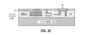
図3A〜図3Eは、本開示の態様による、層転写プロセスの間の集積無線周波数(RF)回路構造300の断面図を示す。図3Aに示すように、RFシリコンオンインシュレータ(SOI)デバイスは、犠牲基板301(たとえば、バルクウエハ)によって支持される埋込み酸化物(BOX)層320上にデバイス310を含む。RF SOIデバイスはまた、第1の誘電体層306内部でデバイス310に結合される相互接続350を含む。図3Bに示すように、ハンドル基板302が、RF SOIデバイスの第1の誘電体層306に接合される。加えて、犠牲基板301が除去される。層転写プロセスを使用して犠牲基板301を除去することで、誘電体の厚さが増加することによって、高性能で低寄生のRFデバイスが可能になる。すなわち、RF SOIデバイスの寄生キャパシタンスは、デバイス310とハンドル基板302との間の距離を決定する誘電体厚さに比例する。
3A-3E show cross-sectional views of the integrated radio frequency (RF)
図3Cに示すように、RF SOIデバイスは、ハンドル基板302が固定されて犠牲基板301が除去された時点で反転される。図3Dに示すように、層転写後の金属被覆プロセスは、たとえば、通常の相補型金属酸化物半導体(CMOS)プロセスを使用して実行される。図3Eに示すように、集積RF回路構造300は、パッシベーション層を堆積させることと、ボンドパッドを開くことと、再配線層(redistribution layer)を堆積させることと、集積RF回路構造300をシステムボード(たとえば、プリント回路板(PCB))に接合することを可能にするために導電バンプ/ピラーを形成することとによって達成される。
As shown in FIG. 3C, the RF SOI device is inverted when the handle substrate 302 is fixed and the
本開示の様々な態様は、集積無線周波数(RF)回路構造のデバイスの裏面へのアクセスをもたらすための層転写および転写後の金属被覆のための技法を提供する。対照的に、基板工程(FEOL)プロセスの間に形成されたデバイスへのアクセスは、従来では、デバイスのゲートおよびソース/ドレイン領域と配線工程(BEOL)相互接続層(たとえば、M1、M2など)との間に接点を設ける中間工程(MEOL)処理の間に設けられる。本開示の態様は、クオリティ(Q)ファクタの高いRFアプリケーションのためのデュアル側面接触キャパシタ(たとえば、MOSキャパシタ)を形成するための層転写後の金属被覆プロセスを伴う。 Various aspects of the disclosure provide techniques for layer transfer and post-transcriptional metal coating to provide access to the backside of the device in an integrated radio frequency (RF) circuit structure. In contrast, access to devices formed during the Front End of Line (FEOL) process has traditionally been the gate and source / drain regions of the device and the Back End of Line (BEOL) interconnect layer (eg, M1, M2, etc.). It is provided during an intermediate process (MEOL) process in which a contact is provided between and. Aspects of the present disclosure involve a post-layer metallization process for forming dual side contact capacitors (eg, MOS capacitors) for RF applications with high quality (Q) factors.
図4は、本開示の態様による、層転写プロセスを使用して製作されたデュアル側面接触キャパシタを含む集積RF回路構造400の断面図である。代表的に、集積RF回路構造400は、第1のプレートとしての半導体層412(たとえば、シリコンオンインシュレータ(SOI)層)と第2のプレートとしてのゲート層408(たとえば、ポリ層)とを有する受動デバイス410(たとえば、MOSキャパシタ)を含む。この配置では、第1のプレート(たとえば、半導体層412)および第2のプレート(たとえば、ゲート層408)は、受動デバイス410を形成するためにキャパシタ誘電体層426(たとえば、高K誘電体)によって分離される。半導体層412、ゲート層408、およびキャパシタ誘電体層426はすべて、絶縁層420上に形成され得る。SOI実装形態では、絶縁層420は埋込み酸化物(BOX)層であり、SOI層は、BOX層(たとえば、絶縁層420)によって支持されるシャロートレンチ分離(STI)領域422を含み得る。
FIG. 4 is a cross-sectional view of an integrated
本明細書で説明するように、MOL/BEOL層は、前面層と呼ばれる。対照的に、絶縁層420を支持する層は、本明細書では裏面層と呼ばれることがある。この用語に従って、集積RF回路構造400はまた、前面金属被覆層によって一緒に結合される、前面金属被覆プラグ418(たとえば、前面タングステンプラグ)を含む前面金属被覆406を含む。前面金属被覆406は、前面接触層430(たとえば、前面シリサイド層)を介してゲート層408に結合され得る。この配置では、前面金属被覆プラグ418は、前面接触層430に結合される。
As described herein, the MOL / BEOL layer is referred to as the front layer. In contrast, the layer that supports the insulating layer 420 is sometimes referred to herein as the backside layer. According to this term, the integrated
図4に示すように、裏面金属被覆414は、裏面接触層432(たとえば、裏面シリサイド層)を介して半導体層412に結合される。裏面シリサイドは、高い抵抗率に起因する問題を低減する。この配置では、裏面金属被覆414は、裏面金属被覆層(たとえば、タングステン)によって一緒に結合された裏面金属被覆プラグ424(たとえば、裏面タングステンプラグ)を含む。前面金属被覆406および裏面金属被覆414は、互いに遠位に正反対に配置され得る。前面接触層は前面シリサイド化を介してゲート層408上に、裏面接触層は裏面シリサイド化を介して半導体層412上に、それぞれ堆積され得る。この配置では、裏面金属被覆プラグ424は裏面接触層432に結合され、裏面金属被覆材料によって一緒に接合される。
As shown in FIG. 4, the back surface metal coating 414 is bonded to the semiconductor layer 412 via the back surface contact layer 432 (for example, the back surface silicide layer). Backside Silicide reduces problems due to high resistivity. In this arrangement, the backside metal coating 414 includes a backside metal coating plug 424 (eg, backside tungsten plug) bonded together by a backside metal coating layer (eg, tungsten). The
本開示の関連態様では、前面金属被覆406は、前面誘電体層404内に配置されてもよく、受動デバイス410のゲート層408に近接する。加えて、裏面金属被覆414は、裏面誘電体層416内に配置された層転写後の金属被覆層であり得る。この配置では、裏面誘電体層416は絶縁層420に隣接し、場合によっては絶縁層420を支持する。加えて、ハンドル基板402は、前面誘電体層404に結合され得る。随意のトラップリッチ層が、前面誘電体層404とハンドル基板402との間に設けられてもよい。ハンドル基板402は、シリコンなどの半導体材料から構成され得る。本開示の一態様では、ハンドル基板は、スイッチトランジスタなど、少なくとも1つの他の能動/受動デバイスを含む。
In a related aspect of the present disclosure, the
図4に示すように、本開示の態様は、受動デバイス410として示される、デュアル側面接触キャパシタ(たとえば、MOSキャパシタ)を形成するための層転写後の金属被覆を説明する。転写後の金属被覆プロセスは、デュアル側面接触キャパシタの第1のプレート(たとえば、半導体層412)に結合された裏面金属被覆を形成し得る。加えて、裏面金属被覆414から遠位の前面金属被覆406は、デュアル側面接触キャパシタの第2のプレート(たとえば、ゲート層408)に結合され得る。この配置では、デュアル側面接触キャパシタは、所望のキャパシタンス密度を達成するために従来のキャパシタ再分割を実行する必要なしに、単一のキャパシタを使用することによって所望のキャパシタンス密度を実現し得る。
As shown in FIG. 4, aspects of the present disclosure describe a post-transcriptional metal coating for forming dual side contact capacitors (eg, MOS capacitors), shown as passive device 410. The post-transcriptional metal coating process can form a back metal coating bonded to a first plate (eg, semiconductor layer 412) of the dual side contact capacitors. In addition, the
図5は、本開示の一態様による集積無線周波数(RF)回路構造を構築する方法500を示すプロセスフロー図である。ブロック502において、受動デバイス(たとえば、MOSキャパシタ)は、犠牲基板上に配設された絶縁層の第1の表面上に製作される。たとえば、図3Aに示すように、デバイス310は、埋込み酸化物(BOX)層上に製作される。図4に示す配置では、受動デバイス410(たとえば、MOSキャパシタ)は、絶縁層420の第1の表面上に配置される。本開示の一態様では、所定のサイズの拡散領域が、第1のMOSキャパシタプレートを設けるために半導体層412内部に形成される。半導体層412内部の拡散領域のサイズは、所望のキャパシタンス密度に従って決定される。次いで、キャパシタ誘電体層426が、半導体層412上に堆積される。次に、ゲート層408(たとえば、ポリシリコン層または金属ゲート層)が、MOSキャパシタ(たとえば、受動デバイス410)の形成を完了するためにキャパシタ誘電体層426上に堆積される。
FIG. 5 is a process flow diagram showing a
ブロック504において、前面シリサイド化プロセスが、デバイスのゲート層の表面上にシリサイドから構成される前面接触層を堆積させるために実行される。たとえば、図4に示すように、前面接触層430が、ゲート層408上に堆積される。ブロック506において、前面金属被覆が、デバイス上の前面誘電体層内に製作される。たとえば、図4に示すように、前面金属被覆406が前面誘電体層404内に製作され、受動デバイス410に結合される。前面金属被覆406は、前面接触層430を介して受動デバイス410に結合され得る。前面金属被覆406は、前面接触層430に結合された前面金属被覆プラグ418(たとえば、前面タングステンプラグ)を含んでもよく、パターニングされた前面誘電体層内に前面金属被覆材料を堆積させることによって一緒に接合される。前面金属被覆406を製作する間、前面誘電体層404がパターニングされ、前面接触層430の所定の部分を露出させるためにエッチングされる。露出されると、第1の前面金属被覆材料が、前面接触層430の露出された所定の部分の上に堆積される。次に、第2の前面金属被覆材料が、前面金属被覆プラグ418上に堆積される。
At
再び図5を参照すると、ブロック508において、ハンドル基板が、前面誘電体層に接合される。たとえば、図4に示すように、ハンドル基板402が、前面誘電体層404に接合される。ブロック510において、犠牲基板が除去される。図3Bに示すように、層転写プロセスは、犠牲基板301の除去を含む。ブロック512において、裏面シリサイド化が、デバイスの半導体層の第1の面上にシリサイドを含む裏面接触層を堆積させるために実行される。たとえば、図4に示すように、裏面接触層432が、半導体層412上に堆積される。
Referring again to FIG. 5, at
ブロック514において、裏面金属被覆が、絶縁層上に製作される。図4に示すように、受動デバイス410が絶縁層420の第1の表面上に製作され、裏面金属被覆414が、ハンドル基板402から遠位にある絶縁層420の対向する面上に製作される。加えて、裏面金属被覆414は、裏面接触層432を介して半導体層412に結合され得る。裏面金属被覆414を製作する間、絶縁層420がパターニングされ、裏面接触層432の所定の部分を露出させるためにエッチングされる。露出されると、第1の裏面金属被覆材料が、裏面金属被覆プラグ424(たとえば、裏面タングステンプラグ)を形成するために裏面接触層432の露出された所定の部分の上に堆積される。次に、第2の裏面金属被覆材料が、裏面金属被覆プラグ424上に堆積される。裏面金属被覆414は、前面金属被覆406に対して遠位にかつ正反対に配置され得る。
In
本開示のさらなる態様によれば、デュアル側面接触キャパシタを含む集積RF回路構造が説明される。集積RF回路構造は、電荷を蓄積するための手段を含む。集積RF回路構造はまた、絶縁層と裏面誘電体層とを含む。電荷蓄積手段は、図4に示す半導体層412およびゲート層408であり得る。別の態様では、前述の手段は、前述の手段によって列挙された機能を実行するように構成される任意のモジュールまたは任意の装置であってもよい。 According to a further aspect of the present disclosure, an integrated RF circuit structure including dual side contact capacitors will be described. The integrated RF circuit structure includes means for accumulating charges. The integrated RF circuit structure also includes an insulating layer and a backside dielectric layer. The charge storage means may be the semiconductor layer 412 and the gate layer 408 shown in FIG. In another aspect, the aforementioned means may be any module or any device configured to perform the functions listed by the aforementioned means.
キャパシタは、電荷を蓄積するために集積回路内で使用される受動素子である。キャパシタは、プレート間の絶縁材料と導電性があるプレートまたは構造を使用して作られることが多い。所与のキャパシタ用の蓄積の量、すなわち、キャパシタンスは、それらのプレートおよび絶縁体を作るために使用される材料、プレートのエリア、およびプレート間の間隔を条件とする。絶縁材料は誘電材料であることが多い。金属酸化物半導体(MOS)キャパシタは、平行プレートキャパシタの一例であり、絶縁体はゲート酸化物であり、プレートはデバイスのボディおよびゲートから作られる。 Capacitors are passive elements used in integrated circuits to store electric charge. Capacitors are often made using insulating material between plates and conductive plates or structures. The amount of accumulation for a given capacitor, ie the capacitance, is conditioned on the materials used to make those plates and insulators, the area of the plates, and the spacing between the plates. The insulating material is often a dielectric material. A metal oxide semiconductor (MOS) capacitor is an example of a parallel plate capacitor, the insulator is a gate oxide, and the plate is made from the body and gate of the device.
MOSキャパシタは、増加したキャパシタンス密度を実現するためにRFアプリケーションにおいて使用される場合がある。残念ながら、進化した相補型MOS(CMOS)処理において使用されるMOSキャパシタは、大きい面積を占有する場合がある。その上、SOIデバイス内のボディのシニングは、MOSキャパシタ性能における制限要因となっているかなりのボディ抵抗を生じる。その結果、1つの大きい面積のキャパシタの代わりに、多くの小さい面積のキャパシタが、所望のキャパシタンス密度を実現するために使用される。このために、チップ空間の非効率的な使用、増加したチップの複雑さ、およびより低いチップ性能がもたらされる。 MOS capacitors may be used in RF applications to achieve increased capacitance densities. Unfortunately, MOS capacitors used in advanced complementary MOS (CMOS) processing can occupy a large area. Moreover, thinning of the body within the SOI device results in significant body resistance that is a limiting factor in MOS capacitor performance. As a result, instead of one large area capacitor, many small area capacitors are used to achieve the desired capacitance density. This results in inefficient use of chip space, increased chip complexity, and lower chip performance.
本開示の態様は、デュアル側面接触キャパシタ(たとえば、MOSキャパシタ)を形成するための層転写後の金属被覆を使用して説明する。転写後の金属被覆プロセスは、キャパシタの第1のプレートに結合された裏面金属被覆を形成し得る。加えて、裏面金属被覆から遠位の前面金属被覆は、キャパシタの第2のプレートに結合され得る。この配置では、デュアル側面接触キャパシタは、所望のキャパシタンス密度を達成するために従来のキャパシタ再分割を実行する必要なしに、単一のキャパシタを使用することによって所望のキャパシタンス密度を実現し得る。 Aspects of the present disclosure will be described using a post-transcriptional metal coating to form dual side contact capacitors (eg, MOS capacitors). The post-transcriptional metallization process can form a backside metallization bonded to the first plate of the capacitor. In addition, the anterior metal coating distal to the back metal coating can be coupled to the second plate of the capacitor. In this arrangement, the dual side contact capacitors can achieve the desired capacitance density by using a single capacitor without the need to perform conventional capacitor subdivision to achieve the desired capacitance density.
この配置では、前面金属被覆はキャパシタの第2のプレートに結合され、キャパシタの第1のプレートに結合された裏面金属被覆から遠位に配置される。本開示の態様では、第1のプレートはシリコンオンインシュレータ(SOI)層から構成され、第2のプレートはゲート層から構成される。裏面金属被覆は、裏面接触層を介してキャパシタの第1のプレートに結合される。前面金属被覆は、前面接触層を介して第2のプレートに結合される。この配置では、キャパシタは、従来のキャパシタ再分割を実行する必要なしに、単一のキャパシタを使用することによって所望のキャパシタンス密度を実現し、それにより、追加のチップ空間、減少したチップの複雑さ、および向上したチップの効率および性能がもたらされる。 In this arrangement, the front metal coating is coupled to the second plate of the capacitor and is located distal to the back metal coating coupled to the first plate of the capacitor. In the aspects of the present disclosure, the first plate is composed of a silicon on insulator (SOI) layer and the second plate is composed of a gate layer. The back metal coating is coupled to the first plate of the capacitor via the back contact layer. The front metal coating is attached to the second plate via the front contact layer. In this arrangement, the capacitors achieve the desired capacitance density by using a single capacitor without the need to perform traditional capacitor subdivision, thereby adding additional chip space and reduced chip complexity. , And improved chip efficiency and performance.
図6は、本開示の一態様が有利に利用される場合がある、例示的なワイヤレス通信システム600を示すブロック図である。説明のために、図6は、3つのリモートユニット620、630、および650、ならびに2つの基地局640を示す。ワイヤレス通信システムがこれよりも多くのリモートユニットおよび基地局を有してもよいことが認識されよう。リモートユニット620、630および650は、開示されたデュアル側面接触キャパシタを含むICデバイス625A、625Cおよび625Bを含む。基地局、スイッチングデバイス、ネットワーク機器などの他のデバイスも、開示されたデュアル側面接触キャパシタを含んでもよいことが認識されよう。図6は、基地局640からリモートユニット620、630、および650への順方向リンク信号680、ならびに、リモートユニット620、630、および650から基地局640への逆方向リンク信号690を示す。
FIG. 6 is a block diagram showing an exemplary
図6では、リモートユニット620はモバイル電話として示され、リモートユニット630はポータブルコンピュータとして示され、リモートユニット650はワイヤレスローカルループシステム内の固定ロケーションリモートユニットとして示される。たとえば、リモートユニットは、モバイル電話、ハンドヘルドパーソナル通信システム(PCS)ユニット、携帯情報端末(PDA)などのポータブルデータユニット、GPS対応デバイス、ナビゲーションデバイス、セットトップボックス、音楽プレーヤ、ビデオプレーヤ、エンターテインメントユニット、メーター読取り機器などの固定ロケーションデータユニット、またはデータもしくはコンピュータ命令を記憶するかもしくは取り出す他の通信デバイス、あるいはそれらの組合せであってもよい。図6は本開示の態様によるリモートユニットを示すが、本開示はこれらの例示的に示されるユニットに限定されない。本開示の態様は、開示されたデュアル側面接触キャパシタを含む、多くのデバイスにおいて適切に採用され得る。
In FIG. 6, the remote unit 620 is shown as a mobile phone, the
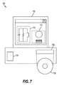
図7は、上で開示されたデュアル側面接触キャパシタなどの半導体構成要素の回路設計、レイアウト設計、および論理設計のために使用される、設計用ワークステーションを示すブロック図である。設計用ワークステーション700は、オペレーティングシステムソフトウェアと、サポートファイルと、CadenceまたはOrCADなどの設計ソフトウェアが入っているハードディスク701を含む。設計用ワークステーション700はまた、回路710、またはデュアル側面接触キャパシタなどの半導体構成要素712の設計を容易にするためにディスプレイ702を含む。回路設計710または半導体構成要素712を有形に記憶するために記憶媒体704が設けられる。回路設計710または半導体構成要素712は、GDSIIやGERBERなどのファイルフォーマットで記憶媒体704上に格納されてもよい。記憶媒体704は、CD−ROM、DVD、ハードディスク、フラッシュメモリ、または他の適切なデバイスであってもよい。さらに、設計用ワークステーション700は、記憶媒体704から入力を受け取るか、または記憶媒体704に出力を書き込むためのドライブ装置703を含む。
FIG. 7 is a block diagram showing a design workstation used for circuit design, layout design, and logic design of semiconductor components such as the dual side contact capacitors disclosed above. The
記憶媒体704上に記録されたデータは、論理回路構成、フォトリソグラフィマスクのためのパターンデータ、または電子ビームリソグラフィなどのシリアル書込みツールのためのマスクパターンデータを指定してもよい。データはさらに、論理シミュレーションに関連したタイミング図やネット回路などの論理検証データを含んでもよい。記憶媒体704上にデータを用意すると、半導体ウエハを設計するためのプロセスの数が減少することによって、回路設計710または半導体構成要素712の設計が容易になる。
The data recorded on the
ファームウェアおよび/またはソフトウェアの実装形態の場合、この方法は、本明細書で説明した機能を実行するモジュール(たとえば、プロシージャ、関数など)を用いて実装されてもよい。本明細書で説明する方法を実施する際に、命令を有形に具現する機械可読媒体が使用されてもよい。たとえば、ソフトウェアコードは、メモリに記憶され、プロセッサユニットによって実行されてもよい。メモリは、プロセッサユニット内に実装されてもよくあるいはプロセッサユニットの外部に実装されてもよい。本明細書において使用される「メモリ」という用語は、長期メモリ、短期メモリ、揮発性メモリ、不揮発性メモリ、または他のメモリのタイプを指し、特定のタイプのメモリもしくは特定の数のメモリ、またはメモリが格納される媒体のタイプに限定すべきではない。 For firmware and / or software implementations, this method may be implemented using modules (eg, procedures, functions, etc.) that perform the functions described herein. Machine-readable media that tangibly embody the instructions may be used in carrying out the methods described herein. For example, the software code may be stored in memory and executed by the processor unit. The memory may be mounted inside the processor unit or outside the processor unit. As used herein, the term "memory" refers to long-term memory, short-term memory, volatile memory, non-volatile memory, or other types of memory, either a particular type of memory or a particular number of memories, or It should not be limited to the type of medium in which the memory is stored.
各機能は、ファームウェアおよび/またはソフトウェアにおいて実装される場合、コンピュータ可読媒体上の1つまたは複数の命令またはコードとして記憶されてもよい。例には、データ構造を用いて符号化されたコンピュータ可読媒体、およびコンピュータプログラムを用いて符号化されたコンピュータ可読媒体が含まれる。コンピュータ可読媒体は、物理的なコンピュータ記憶媒体を含む。記憶媒体は、コンピュータによってアクセスできる入手可能な媒体であってもよい。限定ではなく例として、そのようなコンピュータ可読媒体は、RAM、ROM、EEPROM、CD−ROMもしくは他の光ディスクストレージ、磁気ディスクストレージもしくは他の磁気記憶デバイス、または、所望のプログラムコードを命令もしくはデータ構造の形で記憶するために使用することができるとともに、コンピュータによってアクセスすることができる他の媒体を含むことができ、本明細書において使用されるディスク(disk)およびディスク(disc)は、コンパクトディスク(disc)(CD)、レーザーディスク(登録商標)(disc)、光ディスク(disc)、デジタル多用途ディスク(disc)(DVD)、フロッピーディスク(disk)、およびブルーレイディスク(disc)を含み、ディスク(disk)は通常、データを磁気的に再生し、ディスク(disc)はデータをレーザーを用いて光学的に再生する。上記の組合せもコンピュータ可読媒体の範囲に含まれるべきである。 Each function, when implemented in firmware and / or software, may be stored as one or more instructions or codes on a computer-readable medium. Examples include computer-readable media encoded using data structures and computer-readable media encoded using computer programs. Computer-readable media include physical computer storage media. The storage medium may be an available medium accessible by a computer. By way of example, but not by limitation, such computer readable media instruct or structure RAM, ROM, EEPROM, CD-ROM or other optical disc storage, magnetic disk storage or other magnetic storage device, or desired program code. The discs and discs used herein are compact discs, which can be used to store in the form of, and can include other media accessible by a computer. (Disc) (CD), laser disc (registered trademark) (disc), optical disc (disc), digital versatile disc (disk) (DVD), floppy disc (disk), and Blu-ray disc (disc). The disc) usually reproduces the data magnetically, and the disc) optically reproduces the data using a laser. The above combinations should also be included in the scope of computer readable media.
コンピュータ可読媒体上のストレージに加えて、命令および/またはデータは、通信装置に含まれる伝送媒体上の信号として備えられてもよい。たとえば、通信装置は、命令およびデータを示す信号を有するトランシーバを含んでもよい。命令およびデータは、1つまたは複数のプロセッサに、請求項に概説される機能を実施させるように構成される。 In addition to storage on a computer-readable medium, instructions and / or data may be provided as signals on a transmission medium included in the communication device. For example, a communication device may include a transceiver that has signals indicating instructions and data. Instructions and data are configured to cause one or more processors to perform the functions outlined in the claims.
本開示およびその利点について詳細に説明したが、添付の特許請求の範囲によって定義される本開示の技術から逸脱することなく、明細書において様々な変更、置換、および改変を施すことができることを理解されたい。たとえば、「上」および「下」などの関係語が、基板または電子デバイスに関して使用される。当然、基板または電子デバイスが反転される場合、上は下に、下は上になる。加えて、横向きの場合、上および下は、基板または電子デバイスの側面を指すことがある。さらに、本出願の範囲は、本明細書で説明したプロセス、機械、製造、ならびに組成物、手段、方法、およびステップの特定の構成に限定されることを意図していない。本開示から当業者が容易に諒解するように、本明細書で説明する対応する構成と実質的に同じ機能を実行するかまたは実質的にそれと同じ結果を達成する、現存するかまたは今後開発されるプロセス、機械、製造、組成物、手段、方法、またはステップが、本開示に従って利用されてもよい。したがって、添付の特許請求の範囲は、そのようなプロセス、機械、製造、組成物、手段、方法、またはステップをそれらの範囲内に含むことを意図する。 Although the present disclosure and its advantages have been described in detail, it is understood that various modifications, substitutions, and modifications can be made in the specification without departing from the techniques of the present disclosure as defined by the appended claims. I want to be. For example, related terms such as "top" and "bottom" are used for substrates or electronic devices. Of course, when the substrate or electronic device is flipped, the top is down and the bottom is up. In addition, when in landscape orientation, the top and bottom may refer to the sides of the substrate or electronic device. Moreover, the scope of this application is not intended to be limited to the specific configurations of processes, machines, manufactures, and compositions, means, methods, and steps described herein. As will be readily appreciated by those skilled in the art from this disclosure, any existing or future developed that performs substantially the same function as the corresponding configuration described herein or achieves substantially the same result. Processes, machines, manufactures, compositions, means, methods, or steps may be utilized in accordance with the present disclosure. Therefore, the appended claims are intended to include such processes, machines, manufactures, compositions, means, methods, or steps within them.
100 無線周波数(RF)フロントエンド(RFFE)モジュール
102 電力増幅器
104 デュプレクサ/フィルタ
106 RFスイッチモジュール
108 受動コンバイナ
112 チューナー回路
112A 第1のチューナー回路
112B 第2のチューナー回路
114 アンテナ
115 接地端子
116 キャパシタ
118 インダクタ
120 ワイヤレストランシーバ(WTR)
122 キャパシタ
130 モデム
132 キャパシタ
140 アプリケーションプロセッサ
150 RFフロントエンドモジュール
152 電源
154 クロック
156 電力管理集積回路(PMIC)
158 キャパシタ
160 チップセット
162 キャパシタ
164 キャパシタ
166 インダクタ
170 WiFiモジュール
172 WLANモジュール
174 キャパシタ
180 デュプレクサ
192 アンテナ
194 アンテナ
200 ダイプレクサ
200−1 第1のダイプレクサ
200−2 第2のダイプレクサ
201 システムボード
202 基板
210 アンテナスイッチ(ASW)
210−1 ハイバンドアンテナスイッチ
210−2 ローバンドアンテナスイッチ
212 ハイバンド(HB)入力ポート
214 ローバンド(LB)入力ポート
216 アンテナ
218 電力増幅器
220 RFスイッチ
230 フィルタ
250 RFフロントエンドモジュール
300 RF回路構造
301 犠牲基板
302 ハンドル基板
306 第1の誘電体層
310 デバイス
320 埋込み酸化物(BOX)層
350 相互接続
400 RF回路構造
402 ハンドル基板
404 前面誘電体層
406 前面金属被覆
408 ゲート層
410 受動デバイス
412 半導体層
414 裏面金属被覆
416 裏面誘電体層
418 前面金属被覆プラグ
420 絶縁層
422 シャロートレンチ分離(STI)領域
424 裏面金属被覆プラグ
426 キャパシタ誘電体層
430 前面接触層
432 裏面接触層
600 ワイヤレス通信システム
620 リモートユニット
625A ICデバイス
625B ICデバイス
625C ICデバイス
630 リモートユニット
640 基地局
650 リモートユニット
680 順方向リンク信号
690 逆方向リンク信号
700 設計用ワークステーション
701 ハードディスク
702 ディスプレイ
703 ドライブ装置
704 記憶媒体
710 回路設計
712 半導体構成要素
100 Radio Frequency (RF) Front End (RFFE)
210-1 High-band antenna switch 210-2 Low-
Claims (14)
前記キャパシタの前記第1のプレートに結合された裏面金属被覆と、
前記キャパシタの前記第2のプレートに結合された前面金属被覆であって、前記裏面金属被覆から遠位にかつ正反対に配置される前面金属被覆と、
裏面シリサイド層であって、前記裏面シリサイド層を介して前記裏面金属被覆が前記キャパシタの前記第1のプレートに結合される裏面シリサイド層とを備える、集積回路構造。 A capacitor including a semiconductor layer as a first plate and a gate layer as a second plate separated by a capacitor dielectric layer,
With the back metal coating bonded to the first plate of the capacitor,
A front metal coating coupled to the second plate of the capacitor, wherein the front metal coating is located distal to and opposite to the back metal coating .
An integrated circuit structure comprising a back surface silicide layer, wherein the back surface metal coating is coupled to the first plate of the capacitor via the back surface silicide layer.
絶縁層によって支持され、犠牲基板上に配設される容量性デバイスを製作するステップであって、前記絶縁層上の半導体層内に拡散領域を形成し、前記拡散領域上にデバイス誘電体層を堆積させ、および前記拡散領域上にゲート層を堆積させて前記容量性デバイスを形成する、容量性デバイスを製作するステップと、
前記容量性デバイスの前記ゲート層上に前面接触層を堆積させるステップと、
前記容量性デバイス上であり、前記前面接触層に結合される前面誘電体層内の前面金属被覆を製作するステップと、
前記容量性デバイス上の前記前面誘電体層にハンドル基板を接合するステップと、
前記犠牲基板を除去するステップと、
前記容量性デバイスの前記半導体層上に裏面接触層を堆積させるステップと、
前記絶縁層を支持する裏面誘電体層内に裏面金属被覆を製作するステップであって、前記裏面金属被覆が前記裏面接触層に結合され、前記前面金属被覆から遠位にかつ正反対に配置される、裏面金属被覆を製作するステップとを含む方法。 It is a method of constructing an integrated circuit structure.
It is a step of manufacturing a capacitive device supported by an insulating layer and arranged on a sacrificial substrate, in which a diffusion region is formed in a semiconductor layer on the insulating layer, and a device dielectric layer is formed on the diffusion region. A step of making a capacitive device, which is deposited and a gate layer is deposited on the diffusion region to form the capacitive device .
Depositing a front contact layer on the gate layer of the capacitive device,
A step of making a front metal coating in the front dielectric layer on the capacitive device and coupled to the front contact layer.
The step of joining the handle substrate to the front dielectric layer on the capacitive device,
The step of removing the sacrificial substrate and
Depositing a back contact layer on the semiconductor layer of the capacitive device,
A step of producing a backside metal coating in a backside dielectric layer that supports the insulating layer, where the backside metal coating is coupled to the backside contact layer and placed distally and vice versa from the front surface metal coating. A method including, with the step of making a back metal coating.
前記裏面接触層の所定の部分を露出させるために前記容量性デバイスの前記半導体層に従って前記絶縁層をパターニングするステップと、
前記裏面金属被覆を形成するために、前記パターニングされた絶縁層内部でかつ前記裏面接触層の前記露出された所定の部分の上に裏面金属被覆材料を堆積させるステップと、
前記絶縁層および前記裏面金属被覆の上に前記裏面誘電体層を堆積させるステップとを含む、請求項6に記載の方法。 The step of making the back metal coating is
A step of patterning the insulating layer according to the semiconductor layer of the capacitive device to expose a predetermined portion of the back surface contact layer.
A step of depositing a back metal coating material inside the patterned insulating layer and on the exposed predetermined portion of the back contact layer to form the back metal coating.
The method of claim 6 , comprising depositing the backside dielectric layer on the insulating layer and the backside metal coating.
複数の裏面金属被覆プラグを形成するために、前記裏面接触層の前記露出された所定の部分の上に第1の裏面金属被覆材料を堆積させるステップと、
前記複数の裏面金属被覆プラグ上に第2の裏面金属被覆材料を堆積させるステップとを含む、請求項7に記載の方法。 The step of depositing the back metal coating material is
A step of depositing a first back metal coating material on the exposed predetermined portion of the back contact layer to form a plurality of back metal coating plugs.
The method of claim 7 , comprising depositing a second back metal coating material on the plurality of back metal coating plugs.
前記前面接触層の所定の部分を露出させるために前記容量性デバイスの前記ゲート層に従って前記前面誘電体層をパターニングするステップと、
複数の前面金属被覆プラグを形成するために、前記パターニングされた前面誘電体層内部でかつ前記前面接触層の前記露出された所定の部分の上に第1の前面金属被覆材料を堆積させるステップと、
前記前面金属被覆を形成するために前記複数の前面金属被覆プラグ上に第2の前面金属被覆材料を堆積させるステップとを含む、請求項6に記載の方法。 The step of making the front metal coating is
A step of patterning the front dielectric layer according to the gate layer of the capacitive device to expose a predetermined portion of the front contact layer.
A step of depositing a first front metal coating material inside the patterned front dielectric layer and on the exposed predetermined portion of the front contact layer to form a plurality of front metal coating plugs. ,
And depositing a second front metallization material on the plurality of front metallization plugs in order to form the front metallization process of claim 6.
前記前面誘電体層上にトラップリッチ層を堆積させるステップと、
前記ハンドル基板を前記トラップリッチ層に接合するステップとをさらに含む、請求項6に記載の方法。 The step of joining the handle substrate is
The step of depositing the trap rich layer on the front dielectric layer,
The method of claim 6 , further comprising joining the handle substrate to the trap rich layer.
前記キャパシタに結合されたスイッチトランジスタと、
前記スイッチトランジスタの出力に結合されたアンテナとを備える、無線周波数(RF)フロントエンドモジュール。 The integrated circuit structure according to claim 1, which is an integrated radio frequency (RF) circuit structure, and the integrated circuit structure.
The switch transistor coupled to the capacitor and
A radio frequency (RF) front-end module with an antenna coupled to the output of the switch transistor.
Applications Claiming Priority (3)
| Application Number | Priority Date | Filing Date | Title |
|---|---|---|---|
| US15/240,952 | 2016-08-18 | ||
| US15/240,952 US9847293B1 (en) | 2016-08-18 | 2016-08-18 | Utilization of backside silicidation to form dual side contacted capacitor |
| PCT/US2017/042213 WO2018034756A1 (en) | 2016-08-18 | 2017-07-14 | Utilization of backside silicidation to form dual side contacted capacitor |
Publications (3)
| Publication Number | Publication Date |
|---|---|
| JP2019525476A JP2019525476A (en) | 2019-09-05 |
| JP2019525476A5 JP2019525476A5 (en) | 2020-08-13 |
| JP6921180B2 true JP6921180B2 (en) | 2021-08-18 |
Family
ID=59416818
Family Applications (1)
| Application Number | Title | Priority Date | Filing Date |
|---|---|---|---|
| JP2019505480A Active JP6921180B2 (en) | 2016-08-18 | 2017-07-14 | Utilization of backside silicide to form dual side contact capacitors |
Country Status (7)
| Country | Link |
|---|---|
| US (2) | US9847293B1 (en) |
| EP (1) | EP3501045A1 (en) |
| JP (1) | JP6921180B2 (en) |
| KR (1) | KR20190039714A (en) |
| CN (1) | CN109690788A (en) |
| BR (1) | BR112019002750B1 (en) |
| WO (1) | WO2018034756A1 (en) |
Families Citing this family (1)
| Publication number | Priority date | Publication date | Assignee | Title |
|---|---|---|---|---|
| US9847293B1 (en) | 2016-08-18 | 2017-12-19 | Qualcomm Incorporated | Utilization of backside silicidation to form dual side contacted capacitor |
Family Cites Families (32)
| Publication number | Priority date | Publication date | Assignee | Title |
|---|---|---|---|---|
| US4882649A (en) * | 1988-03-29 | 1989-11-21 | Texas Instruments Incorporated | Nitride/oxide/nitride capacitor dielectric |
| JP3326267B2 (en) | 1994-03-01 | 2002-09-17 | 三菱電機株式会社 | Semiconductor device and manufacturing method thereof |
| US5541442A (en) * | 1994-08-31 | 1996-07-30 | International Business Machines Corporation | Integrated compact capacitor-resistor/inductor configuration |
| JPH08222701A (en) * | 1995-02-17 | 1996-08-30 | Asahi Chem Ind Co Ltd | Semiconductor device having capacitor and manufacture thereof |
| US6320237B1 (en) | 1999-11-08 | 2001-11-20 | International Business Machines Corporation | Decoupling capacitor structure |
| US6984591B1 (en) * | 2000-04-20 | 2006-01-10 | International Business Machines Corporation | Precursor source mixtures |
| DE10210044A1 (en) * | 2002-03-07 | 2003-09-18 | Philips Intellectual Property | Integrated monolithic SOI circuit with capacitor |
| SE527487C2 (en) | 2004-03-02 | 2006-03-21 | Infineon Technologies Ag | A method of producing a capacitor and a monolithic integrated circuit including such a capacitor |
| JP2005260163A (en) | 2004-03-15 | 2005-09-22 | Fujitsu Ltd | Capacitance element and its manufacturing method, semiconductor device and its manufacturing method |
| US20050280087A1 (en) * | 2004-06-16 | 2005-12-22 | Cree Microwave, Inc. | Laterally diffused MOS transistor having source capacitor and gate shield |
| US7064043B1 (en) | 2004-12-09 | 2006-06-20 | Texas Instruments Incorporated | Wafer bonded MOS decoupling capacitor |
| US20060170044A1 (en) | 2005-01-31 | 2006-08-03 | Taiwan Semiconductor Manufacturing Co., Ltd. | One-transistor random access memory technology integrated with silicon-on-insulator process |
| US7345334B2 (en) | 2005-04-27 | 2008-03-18 | International Business Machines Corporation | Integrated circuit (IC) with high-Q on-chip discrete capacitors |
| US7709313B2 (en) | 2005-07-19 | 2010-05-04 | International Business Machines Corporation | High performance capacitors in planar back gates CMOS |
| US8013342B2 (en) * | 2007-11-14 | 2011-09-06 | International Business Machines Corporation | Double-sided integrated circuit chips |
| US20090057742A1 (en) | 2007-08-30 | 2009-03-05 | Sungjae Lee | Cmos varactor |
| CN101952961B (en) * | 2008-02-25 | 2013-01-30 | 飞兆半导体公司 | Micromodules including integrated thin film inductors and methods of making the same |
| US8889548B2 (en) * | 2008-09-30 | 2014-11-18 | Infineon Technologies Ag | On-chip RF shields with backside redistribution lines |
| JP2011193191A (en) * | 2010-03-15 | 2011-09-29 | Renesas Electronics Corp | Semiconductor integrated circuit and high frequency module incorporating the same |
| JP5876249B2 (en) * | 2011-08-10 | 2016-03-02 | ルネサスエレクトロニクス株式会社 | Semiconductor device and manufacturing method of semiconductor device |
| US8916421B2 (en) * | 2011-08-31 | 2014-12-23 | Freescale Semiconductor, Inc. | Semiconductor device packaging having pre-encapsulation through via formation using lead frames with attached signal conduits |
| US20130158378A1 (en) * | 2011-09-22 | 2013-06-20 | The Ohio State University | Ionic barrier for floating gate in vivo biosensors |
| US8592241B2 (en) * | 2011-09-28 | 2013-11-26 | Freescale Semiconductor, Inc. | Method for packaging an electronic device assembly having a capped device interconnect |
| US8748258B2 (en) | 2011-12-12 | 2014-06-10 | International Business Machines Corporation | Method and structure for forming on-chip high quality capacitors with ETSOI transistors |
| US8685790B2 (en) * | 2012-02-15 | 2014-04-01 | Freescale Semiconductor, Inc. | Semiconductor device package having backside contact and method for manufacturing |
| JP6216235B2 (en) * | 2013-05-07 | 2017-10-18 | キヤノン株式会社 | Image forming apparatus, control method therefor, and program |
| US20160043108A1 (en) * | 2014-08-07 | 2016-02-11 | Silanna Semiconductor U.S.A., Inc. | Semiconductor Structure with Multiple Active Layers in an SOI Wafer |
| KR20160034200A (en) * | 2014-09-19 | 2016-03-29 | 가부시키가이샤 한도오따이 에네루기 켄큐쇼 | Method for manufacturing semiconductor device |
| US9257393B1 (en) | 2014-09-29 | 2016-02-09 | Freescale Semiconductor Inc. | Fan-out wafer level packages containing embedded ground plane interconnect structures and methods for the fabrication thereof |
| US9620463B2 (en) * | 2015-02-27 | 2017-04-11 | Qualcomm Incorporated | Radio-frequency (RF) shielding in fan-out wafer level package (FOWLP) |
| US9780210B1 (en) * | 2016-08-11 | 2017-10-03 | Qualcomm Incorporated | Backside semiconductor growth |
| US9847293B1 (en) | 2016-08-18 | 2017-12-19 | Qualcomm Incorporated | Utilization of backside silicidation to form dual side contacted capacitor |
-
2016
- 2016-08-18 US US15/240,952 patent/US9847293B1/en active Active
-
2017
- 2017-07-14 BR BR112019002750-5A patent/BR112019002750B1/en active IP Right Grant
- 2017-07-14 CN CN201780049975.5A patent/CN109690788A/en active Pending
- 2017-07-14 KR KR1020197004314A patent/KR20190039714A/en not_active Application Discontinuation
- 2017-07-14 WO PCT/US2017/042213 patent/WO2018034756A1/en active Search and Examination
- 2017-07-14 EP EP17745583.9A patent/EP3501045A1/en not_active Withdrawn
- 2017-07-14 JP JP2019505480A patent/JP6921180B2/en active Active
- 2017-11-08 US US15/807,169 patent/US10290579B2/en active Active
Also Published As
| Publication number | Publication date |
|---|---|
| US10290579B2 (en) | 2019-05-14 |
| WO2018034756A1 (en) | 2018-02-22 |
| BR112019002750B1 (en) | 2023-04-11 |
| KR20190039714A (en) | 2019-04-15 |
| CN109690788A (en) | 2019-04-26 |
| BR112019002750A2 (en) | 2019-05-14 |
| EP3501045A1 (en) | 2019-06-26 |
| JP2019525476A (en) | 2019-09-05 |
| US9847293B1 (en) | 2017-12-19 |
| US20180076137A1 (en) | 2018-03-15 |
Similar Documents
| Publication | Publication Date | Title |
|---|---|---|
| JP7158373B2 (en) | Backside semiconductor growth | |
| KR102054924B1 (en) | Logic Circuit Block Layouts with Dual-Side Processing | |
| CN109314097B (en) | Method and apparatus for reverse biasing a switching transistor | |
| JP5982585B2 (en) | Diplexer configuration using through-glass via technology | |
| US10256863B2 (en) | Monolithic integration of antenna switch and diplexer | |
| US9812580B1 (en) | Deep trench active device with backside body contact | |
| US10103135B2 (en) | Backside ground plane for integrated circuit | |
| US10840884B2 (en) | Bulk acoustic wave (BAW) and passive-on-glass (POG) filter co-integration | |
| JP6921180B2 (en) | Utilization of backside silicide to form dual side contact capacitors | |
| US10043752B2 (en) | Substrate contact using dual sided silicidation | |
| TW202349628A (en) | Capacitor embedded 3d resonator for broadband filter |
Legal Events
| Date | Code | Title | Description |
|---|---|---|---|
| A521 | Request for written amendment filed |
Free format text: JAPANESE INTERMEDIATE CODE: A523 Effective date: 20190219 |
|
| A521 | Request for written amendment filed |
Free format text: JAPANESE INTERMEDIATE CODE: A523 Effective date: 20200629 |
|
| A621 | Written request for application examination |
Free format text: JAPANESE INTERMEDIATE CODE: A621 Effective date: 20200629 |
|
| A977 | Report on retrieval |
Free format text: JAPANESE INTERMEDIATE CODE: A971007 Effective date: 20201215 |
|
| A131 | Notification of reasons for refusal |
Free format text: JAPANESE INTERMEDIATE CODE: A131 Effective date: 20210125 |
|
| A521 | Request for written amendment filed |
Free format text: JAPANESE INTERMEDIATE CODE: A523 Effective date: 20210426 |
|
| TRDD | Decision of grant or rejection written | ||
| A01 | Written decision to grant a patent or to grant a registration (utility model) |
Free format text: JAPANESE INTERMEDIATE CODE: A01 Effective date: 20210628 |
|
| A61 | First payment of annual fees (during grant procedure) |
Free format text: JAPANESE INTERMEDIATE CODE: A61 Effective date: 20210727 |
|
| R150 | Certificate of patent or registration of utility model |
Ref document number: 6921180 Country of ref document: JP Free format text: JAPANESE INTERMEDIATE CODE: R150 |