JP6911541B2 - Light emitting device and projector - Google Patents
Light emitting device and projector Download PDFInfo
- Publication number
- JP6911541B2 JP6911541B2 JP2017108388A JP2017108388A JP6911541B2 JP 6911541 B2 JP6911541 B2 JP 6911541B2 JP 2017108388 A JP2017108388 A JP 2017108388A JP 2017108388 A JP2017108388 A JP 2017108388A JP 6911541 B2 JP6911541 B2 JP 6911541B2
- Authority
- JP
- Japan
- Prior art keywords
- light
- light emitting
- columnar portion
- emitting device
- columnar
- Prior art date
- Legal status (The legal status is an assumption and is not a legal conclusion. Google has not performed a legal analysis and makes no representation as to the accuracy of the status listed.)
- Active
Links
Images


Classifications
-
- G—PHYSICS
- G03—PHOTOGRAPHY; CINEMATOGRAPHY; ANALOGOUS TECHNIQUES USING WAVES OTHER THAN OPTICAL WAVES; ELECTROGRAPHY; HOLOGRAPHY
- G03B—APPARATUS OR ARRANGEMENTS FOR TAKING PHOTOGRAPHS OR FOR PROJECTING OR VIEWING THEM; APPARATUS OR ARRANGEMENTS EMPLOYING ANALOGOUS TECHNIQUES USING WAVES OTHER THAN OPTICAL WAVES; ACCESSORIES THEREFOR
- G03B21/00—Projectors or projection-type viewers; Accessories therefor
- G03B21/14—Details
- G03B21/20—Lamp housings
- G03B21/2006—Lamp housings characterised by the light source
- G03B21/2013—Plural light sources
-
- F—MECHANICAL ENGINEERING; LIGHTING; HEATING; WEAPONS; BLASTING
- F21—LIGHTING
- F21S—NON-PORTABLE LIGHTING DEVICES; SYSTEMS THEREOF; VEHICLE LIGHTING DEVICES SPECIALLY ADAPTED FOR VEHICLE EXTERIORS
- F21S2/00—Systems of lighting devices, not provided for in main groups F21S4/00 - F21S10/00 or F21S19/00, e.g. of modular construction
-
- F—MECHANICAL ENGINEERING; LIGHTING; HEATING; WEAPONS; BLASTING
- F21—LIGHTING
- F21V—FUNCTIONAL FEATURES OR DETAILS OF LIGHTING DEVICES OR SYSTEMS THEREOF; STRUCTURAL COMBINATIONS OF LIGHTING DEVICES WITH OTHER ARTICLES, NOT OTHERWISE PROVIDED FOR
- F21V29/00—Protecting lighting devices from thermal damage; Cooling or heating arrangements specially adapted for lighting devices or systems
- F21V29/50—Cooling arrangements
- F21V29/502—Cooling arrangements characterised by the adaptation for cooling of specific components
-
- F—MECHANICAL ENGINEERING; LIGHTING; HEATING; WEAPONS; BLASTING
- F21—LIGHTING
- F21V—FUNCTIONAL FEATURES OR DETAILS OF LIGHTING DEVICES OR SYSTEMS THEREOF; STRUCTURAL COMBINATIONS OF LIGHTING DEVICES WITH OTHER ARTICLES, NOT OTHERWISE PROVIDED FOR
- F21V29/00—Protecting lighting devices from thermal damage; Cooling or heating arrangements specially adapted for lighting devices or systems
- F21V29/50—Cooling arrangements
- F21V29/60—Cooling arrangements characterised by the use of a forced flow of gas, e.g. air
-
- F—MECHANICAL ENGINEERING; LIGHTING; HEATING; WEAPONS; BLASTING
- F21—LIGHTING
- F21V—FUNCTIONAL FEATURES OR DETAILS OF LIGHTING DEVICES OR SYSTEMS THEREOF; STRUCTURAL COMBINATIONS OF LIGHTING DEVICES WITH OTHER ARTICLES, NOT OTHERWISE PROVIDED FOR
- F21V7/00—Reflectors for light sources
- F21V7/22—Reflectors for light sources characterised by materials, surface treatments or coatings, e.g. dichroic reflectors
- F21V7/28—Reflectors for light sources characterised by materials, surface treatments or coatings, e.g. dichroic reflectors characterised by coatings
- F21V7/30—Reflectors for light sources characterised by materials, surface treatments or coatings, e.g. dichroic reflectors characterised by coatings the coatings comprising photoluminescent substances
-
- F—MECHANICAL ENGINEERING; LIGHTING; HEATING; WEAPONS; BLASTING
- F21—LIGHTING
- F21V—FUNCTIONAL FEATURES OR DETAILS OF LIGHTING DEVICES OR SYSTEMS THEREOF; STRUCTURAL COMBINATIONS OF LIGHTING DEVICES WITH OTHER ARTICLES, NOT OTHERWISE PROVIDED FOR
- F21V9/00—Elements for modifying spectral properties, polarisation or intensity of the light emitted, e.g. filters
- F21V9/40—Elements for modifying spectral properties, polarisation or intensity of the light emitted, e.g. filters with provision for controlling spectral properties, e.g. colour, or intensity
-
- G—PHYSICS
- G02—OPTICS
- G02B—OPTICAL ELEMENTS, SYSTEMS OR APPARATUS
- G02B5/00—Optical elements other than lenses
- G02B5/20—Filters
-
- G—PHYSICS
- G03—PHOTOGRAPHY; CINEMATOGRAPHY; ANALOGOUS TECHNIQUES USING WAVES OTHER THAN OPTICAL WAVES; ELECTROGRAPHY; HOLOGRAPHY
- G03B—APPARATUS OR ARRANGEMENTS FOR TAKING PHOTOGRAPHS OR FOR PROJECTING OR VIEWING THEM; APPARATUS OR ARRANGEMENTS EMPLOYING ANALOGOUS TECHNIQUES USING WAVES OTHER THAN OPTICAL WAVES; ACCESSORIES THEREFOR
- G03B21/00—Projectors or projection-type viewers; Accessories therefor
- G03B21/14—Details
- G03B21/20—Lamp housings
- G03B21/2006—Lamp housings characterised by the light source
- G03B21/2033—LED or laser light sources
- G03B21/204—LED or laser light sources using secondary light emission, e.g. luminescence or fluorescence
-
- G—PHYSICS
- G03—PHOTOGRAPHY; CINEMATOGRAPHY; ANALOGOUS TECHNIQUES USING WAVES OTHER THAN OPTICAL WAVES; ELECTROGRAPHY; HOLOGRAPHY
- G03B—APPARATUS OR ARRANGEMENTS FOR TAKING PHOTOGRAPHS OR FOR PROJECTING OR VIEWING THEM; APPARATUS OR ARRANGEMENTS EMPLOYING ANALOGOUS TECHNIQUES USING WAVES OTHER THAN OPTICAL WAVES; ACCESSORIES THEREFOR
- G03B21/00—Projectors or projection-type viewers; Accessories therefor
- G03B21/14—Details
- G03B21/20—Lamp housings
- G03B21/2066—Reflectors in illumination beam
-
- G—PHYSICS
- G03—PHOTOGRAPHY; CINEMATOGRAPHY; ANALOGOUS TECHNIQUES USING WAVES OTHER THAN OPTICAL WAVES; ELECTROGRAPHY; HOLOGRAPHY
- G03B—APPARATUS OR ARRANGEMENTS FOR TAKING PHOTOGRAPHS OR FOR PROJECTING OR VIEWING THEM; APPARATUS OR ARRANGEMENTS EMPLOYING ANALOGOUS TECHNIQUES USING WAVES OTHER THAN OPTICAL WAVES; ACCESSORIES THEREFOR
- G03B21/00—Projectors or projection-type viewers; Accessories therefor
- G03B21/14—Details
- G03B21/20—Lamp housings
- G03B21/208—Homogenising, shaping of the illumination light
-
- H—ELECTRICITY
- H01—ELECTRIC ELEMENTS
- H01L—SEMICONDUCTOR DEVICES NOT COVERED BY CLASS H10
- H01L33/00—Semiconductor devices with at least one potential-jump barrier or surface barrier specially adapted for light emission; Processes or apparatus specially adapted for the manufacture or treatment thereof or of parts thereof; Details thereof
- H01L33/48—Semiconductor devices with at least one potential-jump barrier or surface barrier specially adapted for light emission; Processes or apparatus specially adapted for the manufacture or treatment thereof or of parts thereof; Details thereof characterised by the semiconductor body packages
- H01L33/50—Wavelength conversion elements
Description
本発明は、発光装置およびプロジェクターに関する。 The present invention relates to a light emitting device and a projector.
従来、プロジェクターにおいては、光源として超高圧水銀ランプなどの放電ランプが用いられるのが一般的であった。ところが、この種の放電ランプは、寿命が比較的短い、瞬時点灯が難しい、ランプから放射される紫外線が液晶ライトバルブを劣化させる、等の課題がある。そこで、放電ランプに代わる方式の光源を用いたプロジェクターが提案されている。 Conventionally, in a projector, a discharge lamp such as an ultra-high pressure mercury lamp has been generally used as a light source. However, this type of discharge lamp has problems such as a relatively short life, difficulty in instantaneous lighting, and ultraviolet rays emitted from the lamp deteriorating the liquid crystal light bulb. Therefore, a projector using a light source of a type instead of a discharge lamp has been proposed.
例えば特許文献1には、励起光を受けて所定の波長帯域光を発する蛍光体層が形成された発光板と、蛍光体層の上面の法線の方向から励起光を蛍光体層に照射する光源と、を備えたプロジェクターの光源装置(発光装置)が記載されている。 For example, in Patent Document 1, a light emitting plate on which a phosphor layer that receives excitation light and emits light in a predetermined wavelength band is formed, and excitation light is irradiated to the phosphor layer from the direction of the normal line on the upper surface of the phosphor layer. A light source and a light source device (light emitting device) of a projector including the light source are described.
上記のような発光装置では、蛍光体層に光が照射されることにより、蛍光体層の温度が上昇して発光光率が低下する場合がある。このような問題を解決するために、蛍光体層を複数に分割して表面積を大きくし、放熱性を向上させることが考えられる。 In a light emitting device as described above, when the phosphor layer is irradiated with light, the temperature of the phosphor layer may rise and the emission light rate may decrease. In order to solve such a problem, it is conceivable to divide the phosphor layer into a plurality of layers to increase the surface area and improve the heat dissipation.
しかしながら、複数の分割された蛍光体を含む発光装置では、励起光の一部は、蛍光体に入射せずに隣り合う蛍光体の隙間を通って基体に入射するため、発光光率が低下する場合がある。 However, in a light emitting device including a plurality of divided phosphors, a part of the excitation light is incident on the substrate through the gaps between adjacent phosphors without being incident on the phosphors, so that the emission light rate is lowered. In some cases.
本発明のいくつかの態様に係る目的の1つは、発光効率を向上させることができる発光装置を提供することにある。また、本発明のいくつかの態様に係る目的の1つは、高い輝度を有することができるプロジェクターを提供することにある。 One of the objects according to some aspects of the present invention is to provide a light emitting device capable of improving luminous efficiency. Further, one of the objects according to some aspects of the present invention is to provide a projector capable of having high brightness.
本発明に係る発光装置は、
基体と、
光源と、
前記基体に設けられ、前記光源から射出された光により、光を発する第1蛍光体を有する複数の柱状部と、
を含み、
前記光源は、前記柱状部に対し斜めに光を照射する。
The light emitting device according to the present invention
With the base
Light source and
A plurality of columnar portions provided on the substrate and having a first phosphor that emits light by light emitted from the light source.
Including
The light source irradiates the columnar portion with light obliquely.
このような発光装置では、光源から射出された光が柱状部に入射せずに基体に入射することを低減することができる。したがって、このような発光装置では、発光光率を向上させることができる。 In such a light emitting device, it is possible to reduce that the light emitted from the light source does not enter the columnar portion but enters the substrate. Therefore, in such a light emitting device, the light emitting light rate can be improved.
本発明に係る発光装置において、
前記光源から複数の前記柱状部に照射された光の光軸は、前記柱状部の柱方向と交差し
てもよい。
In the light emitting device according to the present invention
The optical axis of the light radiated from the light source to the plurality of pillars may intersect the column direction of the pillars.
このような発光装置では、光源から射出された光が柱状部に入射せずに基体に入射することを低減することができる。 In such a light emitting device, it is possible to reduce that the light emitted from the light source does not enter the columnar portion but enters the substrate.
本発明に係る発光装置において、
前記柱状部は、前記第1蛍光体を挟んで設けられた第1半導体層および第2半導体層を有し、
前記第1半導体層および前記第2半導体層は、前記第1蛍光体が発する光のエネルギーよりも大きいバンドギャップを有し、
前記第1蛍光体、前記第1半導体層、および前記第2半導体層は、前記柱方向に沿って並んでいてもよい。
In the light emitting device according to the present invention
The columnar portion has a first semiconductor layer and a second semiconductor layer provided so as to sandwich the first phosphor.
The first semiconductor layer and the second semiconductor layer have a band gap larger than the energy of light emitted by the first phosphor.
The first phosphor, the first semiconductor layer, and the second semiconductor layer may be arranged along the column direction.
このような発光装置では、第1蛍光体、第1半導体層、および第2半導体層によって量子井戸構造を形成することができ、電子を第1蛍光体に閉じ込めることができる。これにより、このような発光装置では、発光光率を向上させることができる。 In such a light emitting device, a quantum well structure can be formed by the first phosphor, the first semiconductor layer, and the second semiconductor layer, and electrons can be confined in the first phosphor. Thereby, in such a light emitting device, the light emitting light rate can be improved.
本発明に係る発光装置において、
前記柱状部は、
前記光源から照射された光により光を発する第2蛍光体と、
前記第2蛍光体が発する光のエネルギーよりも大きいバンドギャップを有する第3半導体層と、
を有し、
前記第2半導体層および前記第3半導体層は、前記第2蛍光体を挟んで設けられ、
前記第2半導体層は、前記第2蛍光体が発する光のエネルギーよりも大きいバンドギャップを有し、
前記第1蛍光体、前記第2蛍光体、前記第1半導体層、前記第2半導体層、および前記第3半導体層は、前記柱方向に沿って並んでいてもよい。
In the light emitting device according to the present invention
The columnar part is
A second phosphor that emits light by the light emitted from the light source, and
A third semiconductor layer having a bandgap larger than the energy of light emitted by the second phosphor,
Have,
The second semiconductor layer and the third semiconductor layer are provided so as to sandwich the second phosphor.
The second semiconductor layer has a bandgap larger than the energy of light emitted by the second phosphor.
The first phosphor, the second phosphor, the first semiconductor layer, the second semiconductor layer, and the third semiconductor layer may be arranged along the column direction.
このような発光装置では、光源から射出された光は、例えば、隣り合う柱状部において、一方の柱状部の第2蛍光体に入射して一方の柱状部を透過した後、他方の柱状部の第1蛍光体に入射することができる。したがって、このような発光装置では、発光光率を向上させることができる。 In such a light emitting device, for example, in an adjacent columnar portion, the light emitted from the light source is incident on the second phosphor of one columnar portion and transmitted through the one columnar portion, and then the other columnar portion. It can be incident on the first phosphor. Therefore, in such a light emitting device, the light emitting light rate can be improved.
本発明に係る発光装置において、
前記基体の第1面は、凹凸形状を有し、
複数の前記柱状部のうちの第1柱状部は、前記第1面の凹凸形状を構成している第1凸部に設けられ、
複数の前記柱状部のうちの第2柱状部は、前記第1面の凹凸形状を構成している第1凹部に設けられていてもよい。
In the light emitting device according to the present invention
The first surface of the substrate has an uneven shape and has an uneven shape.
The first columnar portion of the plurality of columnar portions is provided on the first convex portion forming the concave-convex shape of the first surface.
The second columnar portion of the plurality of columnar portions may be provided in the first concave portion forming the uneven shape of the first surface.
このような発光装置では、光源から射出された光は、第1柱状部の第1蛍光体に入射して第1柱状部を透過した後、第2柱状部の第1蛍光体に入射することができる。したがって、このような発光装置では、発光光率を向上させることができる。 In such a light emitting device, the light emitted from the light source enters the first phosphor of the first columnar portion, passes through the first columnar portion, and then enters the first phosphor of the second columnar portion. Can be done. Therefore, in such a light emitting device, the light emitting light rate can be improved.
本発明に係る発光装置において、
複数の前記柱状部のうちの第3柱状部は、前記第1面の凹凸形状を構成している第2凸部に設けられ、
複数の前記柱状部のうちの第4柱状部は、前記第1面の凹凸形状を構成している第2凹部に設けられ、
前記柱方向からみて、
前記第2柱状部は、前記第1柱状部の第1方向に設けられ、
前記第4柱状部は、前記第1柱状部の前記第1方向と交差する第2方向に設けられ、
前記第3柱状部は、前記第2柱状部の前記第2方向であって、前記第4柱状部の前記第1方向に設けられ、
前記第1柱状部の中心と前記第2柱状部の中心との間の距離、前記第1柱状部の中心と前記第4柱状部の中心との間の距離、前記第2柱状部の中心と前記第3柱状部の中心との間の距離、および前記第3柱状部の中心と前記第4柱状部の中心との間の距離は、互いに等しくてもよい。
In the light emitting device according to the present invention
The third columnar portion of the plurality of columnar portions is provided on the second convex portion forming the concave-convex shape of the first surface.
The fourth columnar portion of the plurality of columnar portions is provided in the second concave portion forming the uneven shape of the first surface.
Seen from the direction of the pillar
The second columnar portion is provided in the first direction of the first columnar portion.
The fourth columnar portion is provided in a second direction intersecting the first direction of the first columnar portion.
The third columnar portion is provided in the second direction of the second columnar portion, and is provided in the first direction of the fourth columnar portion.
The distance between the center of the first columnar portion and the center of the second columnar portion, the distance between the center of the first columnar portion and the center of the fourth columnar portion, and the center of the second columnar portion. The distance between the center of the third columnar portion and the distance between the center of the third columnar portion and the center of the fourth columnar portion may be equal to each other.
このような発光装置では、第1方向または第2方向から柱状部に光を入射させることにより、凸部に設けられた柱状部の第1蛍光体に入射して該柱状部を透過した光を、凹部に設けられた柱状部の第1蛍光体に入射させることができる。 In such a light emitting device, by injecting light into the columnar portion from the first direction or the second direction, the light incident on the first phosphor of the columnar portion provided on the convex portion and transmitted through the columnar portion is emitted. , It can be incident on the first phosphor of the columnar portion provided in the recess.
本発明に係る発光装置において、
前記柱方向に延出する軸を回転軸として、前記基体を回転させる駆動部を含んでもよい。
In the light emitting device according to the present invention
A drive unit that rotates the substrate may be included with a shaft extending in the direction of the pillar as a rotation axis.
このような発光装置では、光源から射出された光によって柱状部の同じ領域が照射されて該領域が溶解することを抑制することができる。 In such a light emitting device, it is possible to prevent the same region of the columnar portion from being irradiated by the light emitted from the light source and melting the region.
本発明に係る発光装置において、
前記柱方向からみた平面視における前記柱状部の形状は、六角形であってもよい。
In the light emitting device according to the present invention
The shape of the columnar portion in a plan view from the column direction may be hexagonal.
本発明に係る発光装置において、
前記光源は、
光を射出する発光素子と、
前記発光素子から射出された光の光軸を曲げる光学素子と、
を有してもよい。
In the light emitting device according to the present invention
The light source is
A light emitting element that emits light and
An optical element that bends the optical axis of the light emitted from the light emitting element, and
May have.
このような発光装置では、発光素子から射出された光を、光学素子を介して、柱状部に入射させることができる。したがって、このような発光装置では、発光素子の配置の自由度を高くすることができる。 In such a light emitting device, the light emitted from the light emitting element can be incident on the columnar portion via the optical element. Therefore, in such a light emitting device, the degree of freedom in arranging the light emitting elements can be increased.
本発明に係るプロジェクターは、
基体と、
光源と、
前記基体に設けられ、前記光源から射出された光により、光を発する蛍光体を有する複数の柱状部と、
を含み、
前記光源は、前記柱状部に対し斜めに光を照射する。
The projector according to the present invention
With the base
Light source and
A plurality of columnar portions provided on the substrate and having a phosphor that emits light by light emitted from the light source.
Including
The light source irradiates the columnar portion with light obliquely.
このようなプロジェクターでは、高い輝度を有することができる。 Such a projector can have high brightness.
以下、本発明の好適な実施形態について、図面を用いて詳細に説明する。なお、以下に説明する実施形態は、特許請求の範囲に記載された本発明の内容を不当に限定するものではない。また、以下で説明される構成の全てが本発明の必須構成要件であるとは限らない。 Hereinafter, preferred embodiments of the present invention will be described in detail with reference to the drawings. The embodiments described below do not unreasonably limit the content of the present invention described in the claims. Moreover, not all of the configurations described below are essential constituent requirements of the present invention.
1. 第1実施形態
1.1. 発光装置
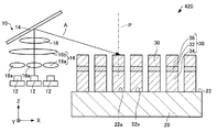
まず、第1実施形態に係る発光装置について、図面を参照しながら説明する。図1は、第1実施形態に係る発光装置100を模式的に示す断面図である。図2は、第1実施形態に係る発光装置100を模式的に示す平面図である。なお、図1は、図2のI−I線断面図である。また、図1および図2では、互いに直交する3軸として、X軸、Y軸、およびZ軸を図示している。
1. 1. First Embodiment 1.1. Light-emitting device First, the light-emitting device according to the first embodiment will be described with reference to the drawings. FIG. 1 is a cross-sectional view schematically showing a
発光装置100は、図1および図2に示すように、光源10と、基体20と、柱状部30と、を含む。なお、便宜上、図2では、光源10の図示を省略している。
As shown in FIGS. 1 and 2, the
光源10は、柱状部30の蛍光体32を励起状態にする光(励起光)Lを射出する。光源10は、基体20の第1面22に対して、斜めに光Lを射出する。具体的には、光源10は、柱状部形成領域22aに対して、斜めに光Lを射出する。柱状部形成領域22aは、基体20の第1面22の柱状部30が設けられている領域である。光源10から射出された光L(以下、単に「光L」ともいう)の光軸Aは、柱状部形成領域22aの法線Pと交差する。図示の例では、法線Pは、Z軸と平行である。光Lは、法線Pと交差した方向から柱状部30に入射する。
The
光源10は、柱状部30に対し斜めに光Lを照射する。ここで、「柱状部30に対し斜めに光Lを照射する。」とは、柱状部30の柱方向に対し斜めに光Lを照射する、すなわち、柱状部30の柱方向と、光Lの光軸Aの方向とが交差するように光を照射することをいう。「柱方向」とは、柱状部30の、法線P方向からみた平面視における底面130の中心点C1と、柱状部30の高さ(法線P方向における最大寸法)の1/2の位置での、柱状部30の、法線P方向からみた平面視における断面132の中心点C2と、を結ぶ中
心線αの方向である。また、底面130の形状が円形以外の場合、「底面130の中心点C1」とは、底面130の形状を内部に含む最小の円(最小包含円)の中心である。また、断面132の形状が円形以外の場合、「断面132の中心点C2」とは、断面132の形状を内部に含む最小の円の中心である。また、「柱状部30の高さの1/2の位置での、柱状部30の断面132」とは、柱状部30の高さの1/2の位置での、柱状部30の中心線αと直交する断面のことである。図示の例では、柱方向は、法線P方向である。
The
光源10から複数の柱状部30に照射された光Lの光軸Aは、柱状部30の柱方向と交差する。光軸Aは、例えば、光Lのうち最も強度が大きい光線と平行な軸である。光軸Aの方向(光軸Aの延出方向)は、基体20の厚さ方向と交差する。法線Pと光軸Aとがなす角度θは、例えば、5°以上45°以下であり、好ましくは、20°以上40°以下である。
The optical axis A of the light L irradiated from the
光源10から射出された(照射された)光Lは、例えば、青色光である。光Lの波長は、例えば、435nm以上480nm以下である。光源10は、例えば、レーザーやLED(Light Emitting Diode)などの発光素子を含んで構成されている。光源10は、発光素子がアレイ状に配列することによって構成されていてもよい。
The light L emitted (irradiated) from the
基体20は、例えば、平板状の形状を有している。基体20は、第1面22を有している。図示の例では、第1面22は、平坦な面である。基体20の材質は、例えば、Al、Cu、GaN、サファイヤなどである。基体20は、サファイヤ基板と、第1面22を有しているGaN層と、が積層されて構成されていてもよい。
The
柱状部30は、基体20の第1面22に設けられている。具体的には、柱状部30は、第1面22の柱状部形成領域22aに設けられている。柱状部形成領域22aは、柱状部30と接している。柱状部30は、例えば、光Lを透過させる材料で構成されている。
The
柱状部30は、第1面22から法線Pの方向に突出した柱状の形状を有している。光Lは、柱状部30の上面(+Z軸方向を向く面)31aおよび側面(上面31aと直交する面)31bに入射する。
The
柱状部30は、複数設けられている。複数の柱状部30は、互いに離間して設けられている。図2に示す例では、複数の柱状部30は、平面視において(Z軸方向からみて)、正方格子状に配列されている。光Lは、平面視において、X軸方向またはY軸方向から柱状部30に入射する。
A plurality of
柱状部30の幅(法線P方向と直交する方向の大きさ)は、例えば、10nm以上5μm以下である。柱状部30の高さ(法線P方向の大きさ)は、例えば、0.1μm以上10μm以下である。隣り合う柱状部30の間隔は、例えば、5nm以上5μm以下である。
The width of the columnar portion 30 (the size in the direction orthogonal to the normal P direction) is, for example, 10 nm or more and 5 μm or less. The height of the columnar portion 30 (the size in the normal P direction) is, for example, 0.1 μm or more and 10 μm or less. The distance between the adjacent
柱状部30の平面形状(Z軸方向からみた形状)は、例えば、円形である。なお、柱状部30の平面形状(法線P方向からみた平面視における柱状部30の形状)は、楕円形であってもよいし、四角形や六角形(図3参照)などの多角形であってもよい。また、図示の例では、柱状部30の幅は、法線P方向において変化していないが、変化していてもよい。
The planar shape (shape seen from the Z-axis direction) of the
柱状部30は、蛍光体32を有している。図示の例は、柱状部30は、蛍光体32によって構成されている。蛍光体32は、光源10から射出された光Lにより光を発する。具体的には、例えば、蛍光体32は、光Lを吸収し、蛍光により光を発する。蛍光は、特に
、蛍光体32の表面において起こる。光Lは、蛍光体32に入射すれば、基体20には入射してもよいし、基体20に入射しなくてもよい。本発明において、蛍光体とは、照射された光により光を発するものをいい、蛍光により光を発するものに限らず、例えば、燐光により光を発するものも含む。
The
蛍光体32が発する光は、例えば、黄色光である。蛍光体32が発する光の波長は、例えば、580nm以上595nm以下である。蛍光体32の材質は、例えば、サイアロン(シリコン、アルミニウム、酸素、および窒素からなるセラミックス材料)、YAG(イットリウムおよびアルミニウムからなるガーネット構造の結晶材料)、InGaNなどである。
The light emitted by the
発光装置100は、例えば、以下の特徴を有する。
The
発光装置100では、基体20に設けられ、光源10から射出された光Lにより、光を発する蛍光体32を有する複数の柱状部30を含み、光源10は、柱状部30に対し斜めに光を照射する。すなわち、柱状部30の柱方向に対し斜めに光を照射する。そのため、発光装置100では、光源10から射出された光Lが柱状部30に入射せずに基体20に入射することを低減することができる。したがって、発光装置100では、発光光率を向上させることができる。よって、発光装置100では、光Lの出力を小さくしても、蛍光体32から射出される光の出力を保つことができる。そのため、発光装置100では、例えば複数の発光素子によって光源10を構成する場合、発光素子の数を少なくすることができる。その結果、発光装置100では、低コスト化を図ることができる。また、発光装置100では、光Lの出力を小さくすることができるので、長寿命化を図ることができる。なお、本発明では、柱状部30の柱方向と光Lの光軸Aの方向とが交差するように、柱状部30に対し光Lを照射することを、柱状部30に対し斜めに光Lを照射する、あるいは、柱状部30の柱方向に対し斜めに光Lを照射する、と表現している。
The
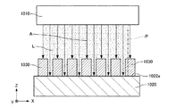
例えば、図4に示すように、光源1010から射出された光Lの光軸Aが柱状部形成領域1022aの法線Pと平行な場合(柱状部1030の柱方向と光軸Aの方向が一致する場合)には、光源1010から照射された光Lの一部は、柱状部1030に入射されずに基体1020に入射される。発光装置100では、図3に示すような発光装置に比べて、発光光率を向上させることができる。
For example, as shown in FIG. 4, when the optical axis A of the light L emitted from the
さらに、発光装置100では、例えば柱状部30を透過した光Lが、該柱状部30と隣り合う柱状部30に入射することができる。したがって、発光装置100では、発光光率を向上させることができる。角度θは、例えば、柱状部30を透過した光Lが、該柱状部30と隣り合う柱状部30に入射するように、適宜設定される。
Further, in the
さらに、発光装置100では、複数の柱状部30は、互いに離間して設けられている。そのため、発光装置100では、複数の柱状部30が互いに連続して設けられている場合に比べて、柱状部30の全表面積(複数の柱状部30の表面積の合計)を大きくすることができる。したがって、発光装置100では、放熱性を向上させることができる。
Further, in the
発光装置100では、光源10から複数の柱状部30に照射された光Lの光軸Aは、柱状部30の柱方向と交差する。そのため、発光装置100では、光Lが柱状部30に入射せずに基体20に入射することを低減することができる。
In the
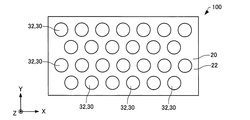
なお、図5に示すように、複数の柱状部30は、平面視において、三角格子状に配列されていてもよい。この場合、光Lは、X軸に対して60°傾いた方向、またはX軸方向から柱状部30に入射する。なお、便宜上、図5では、光源10の図示を省略している。
As shown in FIG. 5, the plurality of
また、図示はしないが、複数の柱状部30は、平面視において、ストライプ状に設けられていてもよい。
Further, although not shown, the plurality of
また、図1に示す例では、柱方向は、法線P方向と一致していたが、これに限定されず、例えば図6に示すように、柱方向は、法線P方向と一致していなくてもよい。図6に示す例では、法線Pと光軸Aとは、平行である。 Further, in the example shown in FIG. 1, the pillar direction coincided with the normal P direction, but the present invention is not limited to this, and for example, as shown in FIG. 6, the pillar direction coincides with the normal P direction. It does not have to be. In the example shown in FIG. 6, the normal line P and the optical axis A are parallel to each other.
また、図1に示す例では、柱状部30のZ軸方向の大きさは、柱状部30のX軸方向の大きさよりも大きかったが、これに限定されず、例えば図7に示すように、柱状部30のZ軸方向の大きさは、柱状部30のX軸方向の大きさよりも小さくてもよい。図7に示す例においても、図1に示す例と同様に、柱方向は、Z軸方向(法線P方向)と一致する。
Further, in the example shown in FIG. 1, the size of the
1.2. 発光装置の製造方法
次に、第1実施形態に係る発光装置100の製造方法について、図面を参照しながら説明する。
1.2. Manufacturing Method of Light Emitting Device Next, a manufacturing method of the
図1に示すように、基体20の第1面22に、複数の柱状部30を形成する。具体的には、まず、例えば、CVD(Chemical Vapor Deposition)法、スパッタ法などにより発光膜(図示せず)を成膜する。次に、例えば、フォトリソグラフィーおよびエッチングにより、発光膜をパターニングする。これにより、複数の柱状部30を形成することができる。
As shown in FIG. 1, a plurality of
次に、第1面22に対して光Lを斜めに射出することができる位置に、光源10を配置する。
Next, the
以上の工程により、発光装置100を製造することができる。
By the above steps, the
なお、柱状部30は、上記の方法に限定されず、例えば、第1面22に所定形状のマスク層(図示せず)を形成し、該マスク層をマスクとして、MOCVD(Metal Organic Chemical Vapor Deposition)法やMBE(Molecular Beam Epitaxy)法などによって結晶成長させて、柱状部30を形成してもよい。
The
また、図6に示すように、柱方向と法線P方向とが一致していない場合は、例えば、斜めエッチングの技術を用いて、柱状部30を形成してもよい。
Further, as shown in FIG. 6, when the column direction and the normal P direction do not match, the
2. 第2実施形態
2.1. 発光装置
次に、第2実施形態に係る発光装置について、図面を参照しながら説明する。図8は、第2実施形態に係る発光装置200を模式的に示す断面図である。なお、図8では、互いに直交する3軸として、X軸、Y軸、およびZ軸を図示している。
2. Second Embodiment 2.1. Light-emitting device Next, the light-emitting device according to the second embodiment will be described with reference to the drawings. FIG. 8 is a cross-sectional view schematically showing the
以下、第2実施形態に係る発光装置200において、上述した発光装置100の構成部材と同様の機能を有する部材については同一の符号を付し、その詳細な説明を省略する。
Hereinafter, in the
上述した発光装置100では、図1に示すように、柱状部30は、蛍光体32によって構成されていた。これに対し、発光装置200では、図8に示すように、柱状部30は、蛍光体32と、第1半導体層34と、第2半導体層36と、を有している。図示の例では、柱状部30は、蛍光体32および半導体層34,36によって構成されている。
In the
第1半導体層34は、基体20の第1面22に設けられている。第1半導体層34および第2半導体層36は、蛍光体32を挟んで設けられている。蛍光体32および半導体層34,36は、法線Pに沿って(柱方向に沿って)並んでいる。
The
第1半導体層34および第2半導体層36は、例えば、蛍光体32のバンドギャップよりも大きなバンドギャップ、あるいは、蛍光体32が発する光のエネルギーよりも大きなバンドギャップを有している。半導体層34,36は、例えば、蛍光体32の屈折率よりも低い屈折率を有している。半導体層34,36は、例えば、蛍光体32に光を閉じ込める(蛍光体32から光が漏れることを抑制する)機能を有するクラッド層である。半導体層34,36は、例えば、GaN層である。蛍光体32は、例えば、InGaN層である。
The
発光装置200では、蛍光体32において発生した光は、例えば、半導体層34,36により法線P方向と直交する方向に伝搬して定在波を形成しレーザー発振する。そして、発光装置200は、例えば、+1次回折光および−1次回折光をレーザー光として、法線P方向に(+Z軸方向側および−Z軸方向側に)射出する。
In the
なお、図示はしないが、基体20と柱状部30との間、または基体20の−Z軸方向側に反射層が設けられていてもよい。該反射層は、例えば、DBR(Distributed Bragg Reflector)層である。該反射層によって、蛍光体32において発生した光を反射させることができ、発光装置200は、例えば、+Z軸方向側からのみ光を射出することができる。
Although not shown, a reflective layer may be provided between the
発光装置200は、上述した発光装置100と同様の効果を有することができる。
The
発光装置200では、柱状部30は、蛍光体32を挟んで設けられた第1半導体層34および第2半導体層36を有し、第1半導体層34および第2半導体層36は、例えば、蛍光体32よりも大きいバンドギャップ、あるいは、蛍光体32が発する光のエネルギーよりも大きなバンドギャップを有している。そのため、発光装置200では、蛍光体32および半導体層34,36によって量子井戸構造を形成することができ、電子を蛍光体32に閉じ込めることができる。これにより、発光装置200では、発光光率を向上させることができる。
In the
さらに、発光装置200では、半導体層34,36は、蛍光体32に光を閉じ込める機能を有するクラッド層である。そのため、発光装置200では、効率よくレーザー発振することができる。
Further, in the
なお、図示はしないが、隣り合う柱状部30の間は、例えば、蛍光体32の屈折率よりも低い屈折率を有する部材によって埋め込まれていてもよい。該部材は、蛍光体32および半導体層34,36よりも放熱性の高い部材であってもよい。
Although not shown, the space between the adjacent
また、図示はしないが、本発明に係る発光装置は、柱状部30は、半導体層34,36によって蛍光体32を挟む構造が法線P方向に繰り返された多重量子井戸構造(MQW)を有していてもよい。この場合、半導体層34,36は、クラッド層として機能せず、柱状部30は、多重量子井戸構造を有する積層体を挟む第1クラッド層および第2クラッド層を別途有していてもよい。
Although not shown, the light emitting device according to the present invention has a multi-quantum well structure (MQW) in which the
2.2. 発光装置の製造方法
次に、第2実施形態に係る発光装置200の製造方法について、説明する。第2実施形
態に係る発光装置200は、基体20の第1面22に、第1半導体層34、蛍光体32、および第2半導体層36を、この順で形成すること以外は、上述した第1実施形態に係る発光装置100の製造方法と、基本的に同じである。しがって、その詳細な説明を省略する。
2.2. Manufacturing Method of Light Emitting Device Next, a manufacturing method of the
2.3. 発光装置の変形例
2.3.1. 第1変形例
次に、第2実施形態の第1変形例に係る発光装置について、図面を参照しながら説明する。図9は、第2実施形態の第1変形例に係る発光装置210を模式的に示す断面図である。なお、図9および以下に示す図10〜図15では、互いに直交する3軸として、X軸、Y軸、およびZ軸を図示している。
2.3. Modification example of the light emitting device 23.1. First Modified Example Next, the light emitting device according to the first modified example of the second embodiment will be described with reference to the drawings. FIG. 9 is a cross-sectional view schematically showing the
以下、第2実施形態の第1変形例に係る発光装置210において、上述した発光装置100,200の構成部材と同様の機能を有する部材については同一の符号を付し、その詳細な説明を省略する。
Hereinafter, in the
上述した発光装置200では、図8に示すように、柱状部30は、1つの蛍光体32と、第1半導体層34と、第2半導体層36と、を有していた。これに対し、発光装置210では、図9に示すように、2つの蛍光体32(第1蛍光体32a、第2蛍光体32b)と、第1半導体層34と、第2半導体層36と、第3半導体層38と、を有している。第3半導体層38の材質は、例えば、半導体層34,36の材質と同じである。
In the
第1半導体層34および第2半導体層36は、第1蛍光体32aを挟んで設けられている。第2半導体層36および第3半導体層38は、第2蛍光体32bを挟んで設けられている。蛍光体32a,32bおよび半導体層34,36,38は、法線Pに沿って並んでいる。
The
第1半導体層34、第2半導体層36、および第3半導体層38は、第1蛍光体32aおよび第2蛍光体32bよりも大きなバンドギャップ、あるいは、蛍光体32a,32bが発する光のエネルギーよりも大きなバンドギャップを有している。半導体層34,36,38は、例えば、蛍光体32a、32bよりも低い屈折率を有している。半導体層34,36は、例えば、第1蛍光体32aに光を閉じ込める機能を有するクラッド層である。半導体層36,38は、例えば、第2蛍光体32bに光を閉じ込める機能を有するクラッド層である。
The
光源10から射出された光Lは、例えば、隣り合う柱状部30において、一方の柱状部30の第2蛍光体32bに入射して一方の柱状部30を透過した後、他方の柱状部30の第1蛍光体32aに入射する。
For example, in the adjacent
発光装置210では、第1蛍光体32aにおいて発生した光は、例えば、半導体層34,36により法線P方向と直交する方向に伝搬して定在波を形成しレーザー発振する。そして、発光装置210は、例えば、+1次回折光および−1次回折光をレーザー光として、法線P方向に射出する。さらに、発光装置210では、第2蛍光体32bにおいて発生した光は、例えば、半導体層36,38により法線P方向と直交する方向に伝搬して定在波を形成しレーザー発振する。そして、発光装置210は、例えば、+1次回折光および−1次回折光をレーザー光として、法線P方向に射出する。
In the
発光装置210は、上述した発光装置200と同様の効果を有することができる。
The
第1半導体層34および第2半導体層36は、第1蛍光体32aを挟んで設けられ、第2半導体層36および第3半導体層38は、第2蛍光体32bを挟んで設けられ、半導体
層34,36,38は、例えば、蛍光体32a,32bよりも大きなバンドギャップ、あるいは、蛍光体32a,32bが発する光のエネルギーよりも大きなバンドギャップを有している。そのため、発光装置210では、光源10から射出された光Lは、例えば、隣り合う柱状部30において、一方の柱状部30の第2蛍光体32bに入射して一方の柱状部30を透過した後、他方の柱状部30の第1蛍光体32aに入射することができる。したがって、発光装置210では、蛍光体32を1つしか有していない場合に比べて、発光光率を向上させることができる。
The
なお、図示はしないが、柱状部30は、3つ以上の蛍光体32を有していてもよい。この場合、3つ以上の蛍光体32の各々は、半導体層34,36,38と同じ材質の半導体層によって挟まれていてもよい。
Although not shown, the
2.3.2. 第2変形例
次に、第2実施形態の第2変形例に係る発光装置について、図面を参照しながら説明する。図10は、第2実施形態の第2変形例に係る発光装置220を模式的に示す断面図である。図11は、第2実施形態の第2変形例に係る発光装置220を模式的に示す平面図である。なお、図10は、図11のX−X線断面図である。また、便宜上、図11では、光源10の図示を省略している。
2.3.2. Second Modified Example Next, the light emitting device according to the second modified example of the second embodiment will be described with reference to the drawings. FIG. 10 is a cross-sectional view schematically showing a
以下、第2実施形態の第2変形例に係る発光装置220において、上述した発光装置100,200,210の構成部材と同様の機能を有する部材については同一の符号を付し、その詳細な説明を省略する。
Hereinafter, in the
上述した発光装置200では、図8に示すように、基体20の第1面22は、平坦な面であった。これに対し、発光装置220では、図10および図11に示すように、基体20の第1面22は、凹凸形状を有している。
In the
第1面22の凹凸形状を構成している凸部23および凹部24は、複数設けられている。凸部23および凹部24の平面形状は、例えば、正方形である。図11に示す例では、複数の凸部23は、互いに連続して設けれ、複数の凹部24は、互いに離間して設けられている。図示はしないが、複数の凸部23は、互いに離間して設けれ、複数の凹部24は、互いに連続して設けられていてもよい。
A plurality of
凸部23および凹部24は、図11に示すように、平面視において、X軸方向に交互に配列されている。さらに、凸部23および凹部24は、平面視において、Y軸方向に交互に配列されている。凸部23および凹部24は、千鳥足状に設けられている。
As shown in FIG. 11, the
凸部23には、柱状部30が設けられている。具体的には、凸部23を構成している柱状部形成領域22aに、柱状部30が設けられている。凹部24には、柱状部30が設けられている。具体的には、凹部24を構成している柱状部形成領域22aに、柱状部30が設けられている。
The
複数の柱状部30のうち第1柱状部30aは、複数の凸部23のうちの第1凸部23aに設けられている。複数の柱状部30のうち第2柱状部30bは、複数の凹部24のうちの第1凹部24aに設けられている。複数の柱状部30のうち第3柱状部30cは、複数の凸部23のうちの第2凸部23bに設けられている。複数の柱状部30のうち第4柱状部30dは、複数の凹部24のうちの第2凹部24bに設けられている。
The first
第1柱状部30aおよび第2柱状部30bは、X軸方向において、隣り合って設けられている。第1柱状部30aおよび第4柱状部30dは、Y軸方向において、隣り合って設けられている。第2柱状部30bおよび第3柱状部30cは、Y軸方向において、隣り合
って設けられている。第3柱状部30cおよび第4柱状部30dは、X軸方向において、隣り合って設けられている。
The first
隣り合う柱状部30において、一方の柱状部30の蛍光体32のZ軸方向の位置、および他方の柱状部30の蛍光体32のZ軸方向の位置は、互いに異なっている。光源10から射出された光Lは、例えば、隣り合う柱状部30において、一方の柱状部30の蛍光体32に入射して一方の柱状部30を透過した後、他方の柱状部30の蛍光体32に入射する。光源10から射出された光Lは、平面視において、X軸方向またはY軸方向から柱状部30に入射する。
In the adjacent
発光装置220では、凸部23に設けられた柱状部30の蛍光体32に入射して該柱状部30を透過した光Lを、凹部24に設けられた柱状部30の蛍光体32に入射させるように、光軸Aと法線Pとのなす角度θを、適宜調整することができる。
In the
平面視において、第2柱状部30bは、第1柱状部30aの第1方向(図示の例では+X軸方向)に設けられている。第4柱状部30dは、第1柱状部30aの第1方向と交差する第2方向(図示の例では−Y軸方向)に設けられている。第3柱状部30cは、第2柱状部30bの−Y軸方向であって、第4柱状部30dの+X軸方向に設けられている。
In a plan view, the second
平面視において、第1柱状部30aの中心O1と第2柱状部30bの中心O2との間の距離、第1柱状部30aの中心O1と第4柱状部30dの中心O4との間の距離、第2柱状部30bの中心O2と第3柱状部30cの中心O3との間の距離、および第3柱状部30cの中心O3と第4柱状部30dの中心O4との間の距離は、互いに等しい。
In a plan view, the distance between the center O1 of the first
図示の例では、平面視において、中心O1,O2を結ぶ線分、中心O1,O4を結ぶ線分、中心O2,O3を結ぶ線分、および中心O3,O4を結ぶ線分は、正方形を構成している。なお、「柱状部30の中心」とは、柱状部30の平面形状が多角形の場合は、その多角形を内部に含む最小の円(半径が最小の円)の中心である。
In the illustrated example, in a plan view, the line segment connecting the centers O1 and O2, the line segment connecting the centers O1 and O4, the line segment connecting the centers O2 and O3, and the line segment connecting the centers O3 and O4 form a square. is doing. When the planar shape of the
発光装置220は、上述した発光装置200と同様の効果を有することができる。
The
発光装置220では、第1柱状部30aは、第1凸部23aに設けられ、第2柱状部30bは、第1凹部24aに設けられている。そのため、発光装置220では、第1柱状部30aの蛍光体32のZ軸方向の位置と、第2柱状部30bの蛍光体32のZ軸方向の位置と、を異ならせることができる。これにより、発光装置220では、光源10から射出された光Lは、第1柱状部30aの蛍光体32に入射して第1柱状部30aを透過した後、第2柱状部30bの蛍光体32に入射することができる。したがって、発光装置220では、発光光率を向上させることができる。
In the
さらに、発光装置220では、第1柱状部30aは、第1凸部23aに設けられ、第2柱状部30bは、第1凹部24aに設けられているため、複数の柱状部30が平坦な面に設けられている場合に比べて、放熱性を向上させることができる。
Further, in the
発光装置220では、第3柱状部30cは、第2凸部23bに設けられ、第4柱状部30dは、第2凹部24bに設けられ、平面視において、第2柱状部30bは、第1柱状部30aの+X軸方向に設けられ、第4柱状部30dは、第1柱状部30aの−Y軸方向に設けられ、第3柱状部30cは、第2柱状部30bの−Y軸方向あって、第4柱状部30dの+X軸方向に設けられ、中心O1,O2間の距離、中心O1,O4間の距離、中心O2,O3間の距離、および中心O3,O4の間の距離は、互いに等しい。そのため、発光装置200では、X軸方向またはY軸方向から柱状部30に光Lを入射させることにより
、凸部23に設けられた柱状部30の蛍光体32に入射して該柱状部30を透過した光Lを、凹部24に設けられた柱状部30の蛍光体32に入射させることができる。このように、発光装置200では、X軸方向またはY軸方向のどちらから光Lを入射させても、発光光率を向上させることができるので、高い汎用性を有することができる。
In the
なお、凸部23および凹部24の配置は、図11に示す例に限定されない。例えば、図12に示すように、凹部24の平面形状は、Y軸方向に長手方向を有する形状を有し、1つの凹部24に複数の柱状部30が設けられていてもよい。図示の例では、凹部24の平面形状は、長方形であり、1つの凹部24に4つの柱状部30が設けられている。凸部23と凹部24とは、図12に示すように、X軸方向に交互に配列されていてもよい。図12に示す場合では、光Lは、X軸に対して45°傾斜した方向、またはX軸方向から柱状部30に入射する。なお、便宜上、図12および以下に示す図13,14では、光源10の図示を省略している。
The arrangement of the
また、図13に示すように、平面視において、複数の柱状部30は、三角格子状に配列されており、複数の凹部24は、三角格子状に配列されていてもよい。この場合、光Lは、X軸に対して60°傾斜した方向、またはX軸方向から柱状部30に入射する。
Further, as shown in FIG. 13, in a plan view, the plurality of
また、図14に示すように、平面視において、複数の柱状部30は、三角格子状に配列されており、X軸に対して45°傾斜した方向に並ぶ複数の柱状部30は、1つの凹部24に設けられていてもよい。凸部23と凹部24とは、図14に示すように、X軸方向に交互に配列されていてもよい。図14に示す場合では、光Lは、X軸に対して60°傾斜した方向、またはX軸方向から柱状部30に入射する。
Further, as shown in FIG. 14, in a plan view, the plurality of
また、図示はしないが、基体20の第1面22は平坦な面であり、複数の柱状部30の高さが異なっていてもよい。
Although not shown, the
2.3.3. 第3変形例
次に、第2実施形態の第3変形例に係る発光装置について、図面を参照しながら説明する。図15は、第2実施形態の第3変形例に係る発光装置230を模式的に示す断面図である。
2.3.3. Third Modified Example Next, the light emitting device according to the third modified example of the second embodiment will be described with reference to the drawings. FIG. 15 is a cross-sectional view schematically showing a
以下、第2実施形態の第2変形例に係る発光装置230において、上述した発光装置100,200,210,220の構成部材と同様の機能を有する部材については同一の符号を付し、その詳細な説明を省略する。
Hereinafter, in the
発光装置230は、図15に示すように、上述した発光装置210と発光装置220とを組み合わせた構成を有している。すなわち、発光装置230では、柱状部30は、第1蛍光体32aと、第2蛍光体32bと、第1半導体層34と、第2半導体層36と、第3半導体層38と、を有している。さらに、発光装置230では、基体20の第1面22は、凹凸形状を有している。
As shown in FIG. 15, the
発光装置230では、例えば発光装置210,220に比べて、より発光光率を向上させることができる。
In the
3. 第3実施形態
3.1. 発光装置
次に、第3実施形態に係る発光装置について、図面を参照しながら説明する。図16は、第3実施形態に係る発光装置300を模式的に示す断面図である。なお、図16では、互いに直交する3軸として、X軸、Y軸、およびZ軸を図示している。
3. 3. Third Embodiment 3.1. Light-emitting device Next, the light-emitting device according to the third embodiment will be described with reference to the drawings. FIG. 16 is a cross-sectional view schematically showing the
以下、第3実施形態に係る発光装置300において、上述した発光装置100の構成部材と同様の機能を有する部材については同一の符号を付し、その詳細な説明を省略する。
Hereinafter, in the
上述した発光装置100では、図1に示すように、柱状部30は、蛍光体32によって構成されていた。これに対し、発光装置300では、図16に示すように、柱状部30は、蛍光体32と、ベース部39と、を有している。図示の例では、柱状部30は、蛍光体32およびベース部39によって構成されている。
In the
ベース部39は、基体20の第1面22に設けられている。ベース部39は、第1面22から+Z軸方向に突出している。ベース部39は、柱状の形状を有している。ベース部39の材質は、例えば、蛍光体32よりも柱状形状を形成しやすい材料であり、具体的には、GaNやInGaNなどの半導体材料である。
The
蛍光体32は、ベース部39を覆って設けられている、蛍光体32は、例えば、ベース部39の外表面(ベース部39の第1面22と接している面以外の面)の全面を覆って設けられている。図示の例では、蛍光体32は、第1面22と接している。
The
発光装置300は、上述した発光装置100と同様の効果を有することができる。
The
発光装置300では、柱状部30は、基体20の第1面22に設けられ、柱状の形状を有するベース部39を有し、蛍光体32は、ベース部39を覆って設けられている。そのため、発光装置300では、柱状部30が蛍光体32のみによって構成されている場合に比べて、ベース部39を、柱状形状を形成しやすい材料で形成することができ、柱状部30のZ軸方向の大きさを大きくすることができる。これにより、発光装置300では、蛍光体32の表面積を大きくすることができ、放熱性を向上させることができる。
In the
3.2. 発光装置の製造方法
次に、第3実施形態に係る発光装置300の製造方法について、説明する。第3実施形態に係る発光装置300は、基体20の第1面22に、MOCVD法やMBE法によりベース部39を形成した後に、ベース部39を覆うように蛍光体32を形成すること以外は、上述した第1実施形態に係る発光装置100の製造方法と、基本的に同じである。しがって、その詳細な説明を省略する。
3.2. Manufacturing Method of Light Emitting Device Next, a manufacturing method of the
4. 第4実施形態
4.1. 発光装置
次に、第4実施形態に係る発光装置について、図面を参照しながら説明する。図17は、第4実施形態に係る発光装置400を模式的に示す断面図である。なお、図17では、互いに直交する3軸として、X軸、Y軸、およびZ軸を図示している。
4. Fourth Embodiment 4.1. Light-emitting device Next, the light-emitting device according to the fourth embodiment will be described with reference to the drawings. FIG. 17 is a cross-sectional view schematically showing the
以下、第4実施形態に係る発光装置400において、上述した発光装置100の構成部材と同様の機能を有する部材については同一の符号を付し、その詳細な説明を省略する。
Hereinafter, in the
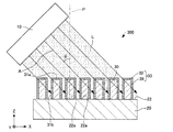
発光装置400では、図17に示すように、光源10は、光を射出する発光素子12と、発光素子12からの光の光軸Aを曲げる光学素子14と、を有している点において、上述した発光装置400と異なる。さらに、発光装置400の光源10は、集光光学系16と、レンズ18と、を有している。
In the
発光素子12は、例えば、レーザー、LEDなどである。発光素子12は、例えば、複数(図示の例では3つ)設けられている。図示の例では、発光素子12は、Z軸方向に光
を射出する。
The
発光素子12から射出された光は、集光光学系16に入射する。集光光学系16は、複数の凸レンズであるレンズ16aと、複数のレンズ16aを介した光が共通して入射する凸レンズであるレンズ16bと、を有している。集光光学系16は、発光素子12から射出された光の光軸A上に配置され、複数の発光素子12から射出された光を集光する。
The light emitted from the
集光光学系16から射出された光は、レンズ18に入射する。レンズ18は、発光素子12から射出された光を、平行化する。
The light emitted from the condensing
レンズ18から射出された光は、光学素子14に入射する。光学素子14は、発光素子12からの光の光軸Aを曲げて、基体20の第1面22に対して斜めに光を反射させる。これにより、光源10は、第1面22に対して斜めに光を射出することができる。光学素子14は、例えば、ミラーである。なお、本発明において、光源10が柱状部30に対して斜めに光Lを照射する、とは、光源10からの光Lが直接、柱状部30に対し斜めに照射することも、光学素子14により光Lの光軸Aを曲げて(光軸Aの方向を変えて)、光源10からの光Lが柱状部に対して斜めに照射されるようにすることも含む表現である。
The light emitted from the
なお、光源10からの光Lが、柱状部30に対して斜めに照射されるのであれば、光学素子14は、ミラーに限定されず、例えば、プリズムや回折格子、ハーフミラーなどであってもよい。また、光学素子14は、計算機合成ホログラム(CGH)であってもよい。光学素子14がCGHである場合は、光源10から射出される光の強度の均一性が高くなるように、光の強度分布を制御してもよい。
If the light L from the
発光装置400は、上述した発光装置100と同様の効果を有することができる。
The
発光装置400では、光源10は、光を射出する発光素子12と、発光素子12から射出された光の光軸Aを曲げる光学素子14と、を有する。そのため、発光装置400では、発光素子12から射出された光を、光学素子14を介して、柱状部30に入射させることができる。したがって、発光装置400では、発光素子12の配置の自由度を高くすることができる。
In the
4.2. 発光装置の製造方法
次に、第4実施形態に係る発光装置400の製造方法について、説明する。第4実施形態に係る発光装置400は、所定の位置に、発光素子12、光学素子14、集光光学系16、およびレンズ18を配置すること以外は、上述した第1実施形態に係る発光装置100の製造方法と、基本的に同じである。しがって、その詳細な説明を省略する。
4.2. Method for Manufacturing Light Emitting Device Next, a method for manufacturing the
4.3. 発光装置の変形例
4.3.1. 第1変形例
次に、第4実施形態の第1変形例に係る発光装置について、図面を参照しながら説明する。図18は、第4実施形態の第1変形例に係る発光装置410を模式的に示す断面図である。なお、図18および以下に示す図19では、互いに直交する3軸として、X軸、Y軸、およびZ軸を図示している。
4.3. Modification example of the light emitting device 4.3.1. First Modified Example Next, the light emitting device according to the first modified example of the fourth embodiment will be described with reference to the drawings. FIG. 18 is a cross-sectional view schematically showing a
以下、第4実施形態の第1変形例に係る発光装置410において、上述した発光装置100,400の構成部材と同様の機能を有する部材については同一の符号を付し、その詳細な説明を省略する。
Hereinafter, in the
発光装置410では、図18に示すように、法線Pと平行な軸(仮想軸)Qを回転軸と
して、基体20を回転させる駆動部40を含む点において、上述した発光装置400と異なる。回転軸Qは、柱方向に延出する軸である。さらに、発光装置400は、支持軸部42を含む。
As shown in FIG. 18, the
駆動部40は、例えば、モーターである。支持軸部42は、駆動部40と基体20とを接続している。支持軸部42は、駆動部40から基体20までZ軸方向に延出している。支持軸部42は、回転軸Q上に設けられている。駆動部40が駆動することにより、支持軸部42が回転する。これにより、基体20は、回転軸Qまわりに回転することができる。回転軸Qは、平面視における基体20の中心を通っていてもよい。図示の例では、柱状部30は、回転軸Qを避けて設けられている。
The
発光装置410は、上述した発光装置400と同様の効果を有することができる。
The
発光装置410では、法線Pと平行な軸Qを回転軸として、基体20を回転させる駆動部40を含む。そのため、発光装置410では、光源10から射出された光によって柱状部30の同じ領域が照射されて該領域が溶解することを抑制することができる。
The
4.3.2. 第2変形例
次に、第4実施形態の第2変形例に係る発光装置について、図面を参照しながら説明する。図19は、第4実施形態の第2変形例に係る発光装置420を模式的に示す断面図である。
4.3.3. Second Modified Example Next, the light emitting device according to the second modified example of the fourth embodiment will be described with reference to the drawings. FIG. 19 is a cross-sectional view schematically showing a
以下、第4実施形態の第1変形例に係る発光装置410において、上述した発光装置100,200,400の構成部材と同様の機能を有する部材については同一の符号を付し、その詳細な説明を省略する。
Hereinafter, in the
発光装置410では、図19に示すように、柱状部30は、蛍光体32と、第1半導体層34と、第2半導体層36と、を有している。
In the
発光装置410は、上述した発光装置200,400と同様の効果を有することができる。
The
なお、図示はしないが、上述した発光装置210,220,230,300において、光源10は、発光素子12、光学素子14、集光光学系16、およびレンズ18を有していてもよい。また、図示はしないが、上述した発光装置100,200,210,220,230,300において、駆動部40および支持軸部42を含んでいてもよい。
Although not shown, in the above-mentioned
5. 第5実施形態
5.1. プロジェクター
次に、第5実施形態に係るプロジェクターについて、図面を参照しながら説明する。図20は、第5実施形態に係るプロジェクター500を模式的に示す図である。
5. Fifth Embodiment 5.1. Projector Next, the projector according to the fifth embodiment will be described with reference to the drawings. FIG. 20 is a diagram schematically showing the
本発明に係るプロジェクターは、本発明に係る発光装置を含む。以下では、本発明に係る発光装置として発光装置400を含むプロジェクター500について説明する。
The projector according to the present invention includes a light emitting device according to the present invention. Hereinafter, the
プロジェクター500は、筐体(図示せず)と、筐体内に備えられている光源モジュール510、色分離光学系520、液晶ライトバルブ(光変調装置)530R,530G,530Bと、色合成素子540、および投射光学系550と、を含む。
The
プロジェクター500は、概略すると以下のように動作する。光源モジュール510か
ら射出された光は、色分離光学系520により複数の色光に分離される。色分離光学系520により分離された複数の色光は、それぞれ対応する液晶ライトバルブ530R,530G,530Bに入射して変調される。液晶ライトバルブ530R,530G,530Bにより変調された複数の色光は、色合成素子540に入射して合成される。色合成素子540により合成された光は、投射光学系550によりスクリーン560に拡大投射され、フルカラーの投射画像が表示される。
The
以下、プロジェクター500の各構成要素について説明する。
Hereinafter, each component of the
光源モジュール510は、発光装置400と、コリメート光学系511と、レンズアレイ512,513と、偏光変換素子514と、重畳レンズ515と、を含む。
The
発光装置400は、光源10から射出された光を受けて蛍光体32から発せられた光を射出する。蛍光体32は、例えば、光源10から射出された青色光を受けて、黄色光を発する。光学素子14は、ハーフミラーである。光源10から射出された青色光の一部は、光学素子14を透過する。
The
コリメート光学系511は、蛍光体32から発せられた光の広がりを抑えるレンズ511aと、レンズ511aから射出された光を平行化するレンズ511bと、を有し、全体として蛍光体32から発せられた光を平行化する。レンズ511a,511bは、凸レンズで構成されている。
The collimating
レンズアレイ512,513は、コリメート光学系511から射出された光の輝度分布を均一化する。レンズアレイ512は、複数のレンズ512aを有している。レンズアレイ513は、複数のレンズ513aを有している。レンズ512aは、レンズ513aと1対1で対応している。コリメート光学系511から射出された光は、複数のレンズ512aに空間的に分かれて入射する。レンズ512aは、入射した光を対応するレンズ513aに結像させる。これにより、複数のレンズ513aの各々に、二次光源像が形成される。なお、レンズ512a,513aの外形形状は、液晶ライトバルブ530R,530G,530Bの画像形成領域の外形形状と略相似形となっている。
The
偏光変換素子514は、レンズアレイ512,513から射出された光の偏光状態を揃える。偏光変換素子514は、例えば、入射した光を、P偏光として射出する。
The
重畳レンズ515は、偏光変換素子514から射出された光を被照明領域にて重畳させる。重畳レンズ515から射出された光は、空間的に分割された後、重畳されることにより輝度分布が均一化される。
The superimposing
色分離光学系520は、ダイクロイックミラー521,522と、ミラー523,524,525,526と、リレーレンズ527,528と、フィールドレンズ529R,529G,529Bと、を含む。ダイクロイックミラー521,522は、例えば、ガラス表面に誘電体多層膜を積層したものである。ダイクロイックミラー521,522は、所定の波長帯域の色光を選択的に反射させ、それ以外の波長帯域の色光を透過させる特性を有している。ここでは、ダイクロイックミラー521,522は、緑色光を反射させる。
The color separation
重畳レンズ515から射出された光は、黄色光Yであり、ダイクロイックミラー521に入射する。黄色光Yのうちの赤色光Rは、ダイクロイックミラー521を通ってミラー523に入射し、ミラー523で反射してフィールドレンズ529Rに入射する。赤色光Rは、フィールドレンズ529Rにより平行化された後に、液晶ライトバルブ530Rに入射する。
The light emitted from the superimposing
黄色光Yのうちの緑色光Gは、ダイクロイックミラー521で反射した後、さらにダイクロイックミラー522で反射してフィールドレンズ529Gに入射する。緑色光Gは、フィールドレンズ529Gにより平行化された後に、液晶ライトバルブ530Gに入射する。
The green light G of the yellow light Y is reflected by the
光学素子14を透過した青色光Bは、ミラー524で反射した後、ダイクロイックミラー521,522、リレーレンズ527を通ってミラー525で反射し、さらに、リレーレンズ528を通ってミラー526で反射してフィールドレンズ529Bに入射する。青色光Bは、フィールドレンズ529Bにより平行化された後に、液晶ライトバルブ530Bに入射する。
The blue light B transmitted through the
液晶ライトバルブ530R,530G,530Bは、例えば、透過型の液晶ライトバルブ等の光変調装置により構成される。液晶ライトバルブ530R,530G,530Bは、画像情報を含んだ画像信号を供給するPC等の信号源(図示略)と電気的に接続されている。液晶ライトバルブ530R,530G,530Bは、供給された画像信号に基づいて、入射光を画素ごとに変調して画像を形成する。液晶ライトバルブ530R,530G,530Bは、それぞれ赤色画像、緑色画像、青色画像を形成する。液晶ライトバルブ530R,530G,530Bにより変調された光(形成された画像)は、色合成素子540に入射する。
The liquid
色合成素子540は、ダイクロイックプリズム等により構成される。ダイクロイックプリズムは、4つの三角柱プリズムが互いに貼り合わされた構造になっている。三角柱プリズムにおいて貼り合わされる面は、ダイクロイックプリズムの内面になる。ダイクロイックプリズムの内面に、赤色光が反射し緑色光が透過するミラー面と、青色光が反射し緑色光が透過するミラー面とが互いに直交して形成されている。ダイクロイックプリズムに入射した緑色光は、ミラー面を通ってそのまま射出される。ダイクロイックプリズムに入射した赤色光、青色光は、ミラー面で選択的に反射あるいは透過して、緑色光の射出方向と同じ方向に射出される。このようにして3つの色光(画像)が重ね合わされて合成され、合成された色光が投射光学系550によってスクリーン560に拡大投射される。
The
プロジェクター500は、発光効率を向上させることができる発光装置400を含む。そのため、プロジェクター500は、高い輝度を有することができる。
The
プロジェクター500では、光学素子14は、ハーフミラーである。そのため、プロジェクター500では、光源モジュール510を複数用いなくても、赤色光、緑色光、および青色光を射出することができ、小型化を図ることができる。
In the
なお、上記の例では、光変調装置として透過型の液晶ライトバルブを用いたが、液晶以外のライトバルブを用いてもよいし、反射型のライトバルブを用いてもよい。このようなライトバルブとしては、例えば、反射型の液晶ライトバルブや、デジタルマイクロミラーデバイス(Digital Micromirror Device)が挙げられる。また、投射光学系の構成は、使用されるライトバルブの種類によって適宜変更される。 In the above example, a transmissive liquid crystal light bulb is used as the light modulation device, but a light bulb other than the liquid crystal may be used, or a reflective light bulb may be used. Examples of such a light bulb include a reflective liquid crystal light bulb and a digital micromirror device (Digital Micromirror Device). Further, the configuration of the projection optical system is appropriately changed depending on the type of the light bulb used.
5.2. プロジェクターの変形例
5.2.1. 第1変形例
次に、第5実施形態の第1変形例に係るプロジェクターについて、図面を参照しながら説明する。図21は、第5実施形態の第1変形例に係るプロジェクター600を模式的に示す図である。
5.2. Deformation example of projector 5.2.1. First Modified Example Next, the projector according to the first modified example of the fifth embodiment will be described with reference to the drawings. FIG. 21 is a diagram schematically showing a
以下、第5実施形態の第1変形例に係るプロジェクター600において、上述したプロジェクター500の構成部材と同様の機能を有する部材については同一の符号を付し、その詳細な説明を省略する。
Hereinafter, in the
上述したプロジェクター500では、図20に示すように、発光装置400を含んでいた。これに対し、プロジェクター600では、図21に示すように、発光装置410を含む。なお、本発明に係るプロジェクターは、発光装置400,410に限定されず、本発明に係る発光装置を含むことができる。
As shown in FIG. 20, the
プロジェクター600は、上述したプロジェクター500と同様の効果を有することができる。
The
プロジェクター600では、発光装置410を含むため、光源10から射出された光によって柱状部30の同じ領域が照射されて該領域が溶解することを抑制することができる。
Since the
5.2.2. 第2変形例
次に、第5実施形態の第2変形例に係るプロジェクターについて、図面を参照しながら説明する。図22は、第5実施形態の第2変形例に係るプロジェクター700を模式的に示す図である。
5.2.2. Second Modified Example Next, the projector according to the second modified example of the fifth embodiment will be described with reference to the drawings. FIG. 22 is a diagram schematically showing a
以下、第5実施形態の第2変形例に係るプロジェクター700において、上述したプロジェクター500,600の構成部材と同様の機能を有する部材については同一の符号を付し、その詳細な説明を省略する。
Hereinafter, in the
上述したプロジェクター500では、図20に示すように、光学素子14は、ハーフミラーであった。これに対し、プロジェクター700では、図22に示すように、光学素子14は、ミラーであり、発光素子12から射出された光を透過しない。
In the
プロジェクター700では、光源モジュール710を含む。光源モジュール710は、発光素子12と、集光光学系16と、レンズアレイ512,513と、偏光変換素子514と、 重畳レンズ515と、を含む。光源モジュール710は、青色光Bを射出する。光源モジュール710から射出された青色光Bは、フィールドレンズ529Rを通って、液晶ライトバルブ530Bに入射する。
The
なお、プロジェクター700では、光源モジュール510は、発光装置410を含む。また、色分離光学系520は、ダイクロイックミラー522、ミラー524,525,526、およびリレーレンズ527,528を有しておらず、緑色光Gを反射させるミラー722を有している。
In the
プロジェクター700は、上述したプロジェクター500と同様の効果を有することができる。
The
5.2.3. 第3変形例
次に、第5実施形態の第3変形例に係るプロジェクターについて、図面を参照しながら説明する。図23は、第5実施形態の第3変形例に係るプロジェクター800を模式的に示す図である。
5.2.2. Third Modified Example Next, the projector according to the third modified example of the fifth embodiment will be described with reference to the drawings. FIG. 23 is a diagram schematically showing the
以下、第5実施形態の第3変形例に係るプロジェクター800において、上述したプロジェクター500,600,700の構成部材と同様の機能を有する部材については同一
の符号を付し、その詳細な説明を省略する。
Hereinafter, in the
上述したプロジェクター500では、図20に示すように、発光装置400を含んでいた。これに対し、プロジェクター800では、図23に示すように、発光装置420を含む。
As shown in FIG. 20, the
発光装置420は、コリメート光(略コリメート光)のレーザー光を射出することができる。したがって、プロジェクター800の光源モジュール510は、図20に示すプロジェクター500の光源モジュール510のように、コリメート光学系511を設ける必要がない。プロジェクター800の光源モジュール510は、発光装置420から射出された光を拡散させる拡散レンズ811を含んでいる。
The
なお、プロジェクター800では、光学素子14は、ミラーであり、光源モジュール710を含む。また、色分離光学系520は、ダイクロイックミラー522、ミラー524,525,526、およびリレーレンズ527,528を有しておらず、緑色光Gを反射させるミラー722を有している。
In the
プロジェクター800は、上述したプロジェクター500と同様の効果を有することができる。
The
プロジェクター800は、レーザー光を射出することができる発光装置420を含む。そのため、プロジェクター800では、上述したプロジェクター500のように、コリメート光学系511を設ける必要がない。これにより、プロジェクター800では、発光装置420と、発光装置420から射出された光が直後に入射する部材(図示の例では拡散レンズ811)と、の間の距離を大きくすることができる。したがって、プロジェクター800では、例えば、発光装置420と光学素子14との間の距離を小さくすることができ、基体20の第1面22に対して、光を斜めに射出しやすくすることができる。
The
本発明は、本願に記載の特徴や効果を有する範囲で一部の構成を省略したり、各実施形態や変形例を組み合わせたりしてもよい。 In the present invention, some configurations may be omitted, or each embodiment or modification may be combined within the range having the features and effects described in the present application.
本発明は、実施の形態で説明した構成と実質的に同一の構成(例えば、機能、方法及び結果が同一の構成、あるいは目的及び効果が同一の構成)を含む。また、本発明は、実施の形態で説明した構成の本質的でない部分を置き換えた構成を含む。また、本発明は、実施の形態で説明した構成と同一の作用効果を奏する構成又は同一の目的を達成することができる構成を含む。また、本発明は、実施の形態で説明した構成に公知技術を付加した構成を含む。 The present invention includes a configuration substantially the same as the configuration described in the embodiment (for example, a configuration having the same function, method and result, or a configuration having the same purpose and effect). The present invention also includes a configuration in which a non-essential part of the configuration described in the embodiment is replaced. The present invention also includes a configuration that exhibits the same effects as the configuration described in the embodiment or a configuration that can achieve the same object. Further, the present invention includes a configuration in which a known technique is added to the configuration described in the embodiment.
10…光源、12…発光素子、14…光学素子、16…集光光学系、16a,16b…レンズ、18…レンズ、20…基体、22…第1面、22a…柱状部形成領域、23…凸部、23a…第1凸部、23b…第2凸部、24…凹部、24a…第1凹部、24b…第2凹部、30…柱状部、30a…第1柱状部、30b…第2柱状部、30c…第3柱状部、30d…第4柱状部、31a…上面、31b…側面、32…蛍光体、32a…第1蛍光体、32b…第2蛍光体、34…第1半導体層、36…第2半導体層、38…第3半導体層、39…ベース部、40…駆動部、42…支持軸部、100…発光装置、130…底面、132…断面、200,210,220,230,300,400,410,420…発光装置、500…プロジェクター、510…光源モジュール、511…コリメート光学系、511a,511b…レンズ、512…レンズアレイ、512a…レンズ、513…レンズアレイ、513a…レンズ、514…偏光変換素子、515…重畳レンズ、520…
色分離光学系、521,522…ダイクロイックミラー、523,524,525,526…ミラー、527,528…リレーレンズ、529R,529G,529B…フィールドレンズ、530R,530G,530B…液晶ライトバルブ、540…色合成素子、550…投射光学系、560…スクリーン、600,700…プロジェクター、710…光源モジュール、722…ミラー、800…プロジェクター、811…拡散レンズ、1010…光源、1020…基体、1022a…柱状部形成領域、1030…柱状部
10 ... light source, 12 ... light emitting element, 14 ... optical element, 16 ... condensing optical system, 16a, 16b ... lens, 18 ... lens, 20 ... substrate, 22 ... first surface, 22a ... columnar portion forming region, 23 ... Convex part, 23a ... 1st convex part, 23b ... 2nd convex part, 24 ... concave part, 24a ... 1st concave part, 24b ... 2nd concave part, 30 ... columnar part, 30a ... 1st columnar part, 30b ... 2nd columnar part Part, 30c ... 3rd columnar portion, 30d ... 4th columnar portion, 31a ... upper surface, 31b ... side surface, 32 ... phosphor, 32a ... first phosphor, 32b ... second phosphor, 34 ... first semiconductor layer, 36 ... 2nd semiconductor layer, 38 ... 3rd semiconductor layer, 39 ... base part, 40 ... drive part, 42 ... support shaft part, 100 ... light source, 130 ... bottom surface, 132 ... cross section, 200, 210, 220, 230 , 300, 400, 410, 420 ... light emitting device, 500 ... projector, 510 ... light source module, 511 ... collimating optical system, 511a, 511b ... lens, 512 ... lens array, 512a ... lens, 513 ... lens array, 513a ...
Color separation optics, 521,522 ... Dichroic mirror, 523,524,525,526 ... Mirror, 527,528 ... Relay lens, 529R, 529G, 529B ... Field lens, 530R, 530G, 530B ... Liquid crystal light valve, 540 ... Color synthesis element, 550 ... Projection optics, 560 ... Screen, 600, 700 ... Projector, 710 ... Light source module, 722 ... Mirror, 800 ... Projector, 811 ... Diffuse lens, 1010 ... Light source, 1020 ... Base, 1022a ... Columnar part Forming region, 1030 ... Columnar part
Claims (8)
光源と、
前記基体に設けられ、前記光源から射出された光により、光を発する第1蛍光体を有する複数の柱状部と、
を含み、
前記光源は、前記柱状部に対し斜めに光を照射し、
前記光源から複数の前記柱状部に照射された光の光軸は、前記柱状部の柱方向と交差し、
前記柱状部は、前記第1蛍光体を挟んで設けられた第1半導体層および第2半導体層を有し、
前記第1半導体層および前記第2半導体層は、前記第1蛍光体が発する光のエネルギーよりも大きいバンドギャップを有し、
前記第1蛍光体、前記第1半導体層、および前記第2半導体層は、前記柱方向に沿って並んでいる、発光装置。 With the base
Light source and
A plurality of columnar portions provided on the substrate and having a first phosphor that emits light by light emitted from the light source.
Including
The light source irradiates the columnar portion with light at an angle .
The optical axes of the light radiated from the light source to the plurality of columnar portions intersect with the columnar directions of the columnar portions.
The columnar portion has a first semiconductor layer and a second semiconductor layer provided so as to sandwich the first phosphor.
The first semiconductor layer and the second semiconductor layer have a band gap larger than the energy of light emitted by the first phosphor.
A light emitting device in which the first phosphor, the first semiconductor layer, and the second semiconductor layer are arranged along the column direction.
前記柱状部は、
前記光源から照射された光により光を発する第2蛍光体と、
前記第2蛍光体が発する光のエネルギーよりも大きいバンドギャップを有する第3半導体層と、
を有し、
前記第2半導体層および前記第3半導体層は、前記第2蛍光体を挟んで設けられ、
前記第2半導体層は、前記第2蛍光体が発する光のエネルギーよりも大きいバンドギャップを有し、
前記第1蛍光体、前記第2蛍光体、前記第1半導体層、前記第2半導体層、および前記第3半導体層は、前記柱方向に沿って並んでいる、発光装置。 In claim 1 ,
The columnar part is
A second phosphor that emits light by the light emitted from the light source, and
A third semiconductor layer having a bandgap larger than the energy of light emitted by the second phosphor,
Have,
The second semiconductor layer and the third semiconductor layer are provided so as to sandwich the second phosphor.
The second semiconductor layer has a bandgap larger than the energy of light emitted by the second phosphor.
A light emitting device in which the first phosphor, the second phosphor, the first semiconductor layer, the second semiconductor layer, and the third semiconductor layer are arranged along the column direction.
前記基体の第1面は、凹凸形状を有し、
複数の前記柱状部のうちの第1柱状部は、前記第1面の凹凸形状を構成している第1凸部に設けられ、
複数の前記柱状部のうちの第2柱状部は、前記第1面の凹凸形状を構成している第1凹部に設けられている、発光装置。 In claim 1 or 2 ,
The first surface of the substrate has an uneven shape and has an uneven shape.
The first columnar portion of the plurality of columnar portions is provided on the first convex portion forming the concave-convex shape of the first surface.
The second columnar portion of the plurality of columnar portions is a light emitting device provided in the first concave portion forming the concave-convex shape of the first surface.
複数の前記柱状部のうちの第3柱状部は、前記第1面の凹凸形状を構成している第2凸部に設けられ、
複数の前記柱状部のうちの第4柱状部は、前記第1面の凹凸形状を構成している第2凹部に設けられ、
前記柱方向からみて、
前記第2柱状部は、前記第1柱状部の第1方向に設けられ、
前記第4柱状部は、前記第1柱状部の前記第1方向と交差する第2方向に設けられ、
前記第3柱状部は、前記第2柱状部の前記第2方向であって、前記第4柱状部の前記第1方向に設けられ、
前記第1柱状部の中心と前記第2柱状部の中心との間の距離、前記第1柱状部の中心と前記第4柱状部の中心との間の距離、前記第2柱状部の中心と前記第3柱状部の中心との間の距離、および前記第3柱状部の中心と前記第4柱状部の中心との間の距離は、互いに等しい、発光装置。 In claim 3 ,
The third columnar portion of the plurality of columnar portions is provided on the second convex portion forming the concave-convex shape of the first surface.
The fourth columnar portion of the plurality of columnar portions is provided in the second concave portion forming the uneven shape of the first surface.
Seen from the direction of the pillar
The second columnar portion is provided in the first direction of the first columnar portion.
The fourth columnar portion is provided in a second direction intersecting the first direction of the first columnar portion.
The third columnar portion is provided in the second direction of the second columnar portion, and is provided in the first direction of the fourth columnar portion.
The distance between the center of the first columnar portion and the center of the second columnar portion, the distance between the center of the first columnar portion and the center of the fourth columnar portion, and the center of the second columnar portion. A light emitting device in which the distance between the center of the third columnar portion and the distance between the center of the third columnar portion and the center of the fourth columnar portion are equal to each other.
前記柱方向に延出する軸を回転軸として、前記基体を回転させる駆動部を含む、発光装置。 In any one of claims 1 to 4 ,
A light emitting device including a drive unit that rotates the substrate with a shaft extending in the direction of the pillar as a rotation axis.
前記柱方向からみた平面視における前記柱状部の形状は、六角形である、発光装置。 In any one of claims 1 to 5 ,
A light emitting device in which the shape of the columnar portion in a plan view seen from the column direction is a hexagon.
前記光源は、
光を射出する発光素子と、
前記発光素子から射出された光の光軸を曲げる光学素子と、
を有する、発光装置。 In any one of claims 1 to 6 ,
The light source is
A light emitting element that emits light and
An optical element that bends the optical axis of the light emitted from the light emitting element, and
A light emitting device.
光源と、
前記基体に設けられ、前記光源から射出された光により、光を発する蛍光体を有する複数の柱状部と、
を含み、
前記光源は、前記柱状部に対し斜めに光を照射し、
前記光源から複数の前記柱状部に照射された光の光軸は、前記柱状部の柱方向と交差し、
前記柱状部は、前記第1蛍光体を挟んで設けられた第1半導体層および第2半導体層を有し、
前記第1半導体層および前記第2半導体層は、前記第1蛍光体が発する光のエネルギーよりも大きいバンドギャップを有し、
前記第1蛍光体、前記第1半導体層、および前記第2半導体層は、前記柱方向に沿って並んでいる、プロジェクター。 With the base
Light source and
A plurality of columnar portions provided on the substrate and having a phosphor that emits light by light emitted from the light source.
Including
The light source irradiates the columnar portion with light at an angle .
The optical axes of the light radiated from the light source to the plurality of columnar portions intersect with the columnar directions of the columnar portions.
The columnar portion has a first semiconductor layer and a second semiconductor layer provided so as to sandwich the first phosphor.
The first semiconductor layer and the second semiconductor layer have a band gap larger than the energy of light emitted by the first phosphor.
A projector in which the first phosphor, the first semiconductor layer, and the second semiconductor layer are arranged along the column direction.
Priority Applications (4)
| Application Number | Priority Date | Filing Date | Title |
|---|---|---|---|
| JP2017108388A JP6911541B2 (en) | 2017-05-31 | 2017-05-31 | Light emitting device and projector |
| US16/618,203 US10942432B2 (en) | 2017-05-31 | 2018-05-22 | Light emitting apparatus and projector |
| CN201880034987.5A CN110710068A (en) | 2017-05-31 | 2018-05-22 | Light emitting device and projector |
| PCT/JP2018/019636 WO2018221316A1 (en) | 2017-05-31 | 2018-05-22 | Light-emitting device and projector |
Applications Claiming Priority (1)
| Application Number | Priority Date | Filing Date | Title |
|---|---|---|---|
| JP2017108388A JP6911541B2 (en) | 2017-05-31 | 2017-05-31 | Light emitting device and projector |
Publications (3)
| Publication Number | Publication Date |
|---|---|
| JP2018205438A JP2018205438A (en) | 2018-12-27 |
| JP2018205438A5 JP2018205438A5 (en) | 2020-07-27 |
| JP6911541B2 true JP6911541B2 (en) | 2021-07-28 |
Family
ID=64454578
Family Applications (1)
| Application Number | Title | Priority Date | Filing Date |
|---|---|---|---|
| JP2017108388A Active JP6911541B2 (en) | 2017-05-31 | 2017-05-31 | Light emitting device and projector |
Country Status (4)
| Country | Link |
|---|---|
| US (1) | US10942432B2 (en) |
| JP (1) | JP6911541B2 (en) |
| CN (1) | CN110710068A (en) |
| WO (1) | WO2018221316A1 (en) |
Families Citing this family (2)
| Publication number | Priority date | Publication date | Assignee | Title |
|---|---|---|---|---|
| JP6989786B2 (en) | 2019-01-30 | 2022-01-12 | 日亜化学工業株式会社 | Wavelength conversion parts and light emitting devices using them |
| JP2023058756A (en) * | 2020-03-10 | 2023-04-26 | シャープ株式会社 | Optical element and light emission system |
Family Cites Families (24)
| Publication number | Priority date | Publication date | Assignee | Title |
|---|---|---|---|---|
| JP2003020476A (en) | 2001-07-10 | 2003-01-24 | Nippon Hoso Kyokai <Nhk> | Fluorescent thin film, electroluminescent thin-film display device, field emission-type display device and method for forming fluorescent thin film |
| JP4789372B2 (en) * | 2001-08-27 | 2011-10-12 | キヤノン株式会社 | Radiation detection apparatus, system, and scintillator panel provided in them |
| CN1817065A (en) * | 2003-07-02 | 2006-08-09 | 松下电器产业株式会社 | Electroluminescent device and display |
| JP4365255B2 (en) * | 2004-04-08 | 2009-11-18 | 浜松ホトニクス株式会社 | Luminescent body, electron beam detector, scanning electron microscope and mass spectrometer using the same |
| JP2006104411A (en) | 2004-10-08 | 2006-04-20 | Sharp Corp | Phosphor, its manufacturing method and light-emitting device using the same |
| JP2006179658A (en) * | 2004-12-22 | 2006-07-06 | Mitsubishi Electric Corp | Light emitting device |
| US7663148B2 (en) * | 2006-12-22 | 2010-02-16 | Philips Lumileds Lighting Company, Llc | III-nitride light emitting device with reduced strain light emitting layer |
| JP5253740B2 (en) | 2007-01-09 | 2013-07-31 | 学校法人上智学院 | Method for producing group III nitride semiconductor fine columnar crystal and group III nitride structure |
| JP5043472B2 (en) | 2007-02-28 | 2012-10-10 | 学校法人上智学院 | Method for producing group III nitride semiconductor fine columnar crystal and group III nitride structure |
| JP2009076896A (en) * | 2007-08-31 | 2009-04-09 | Panasonic Corp | Semiconductor light-emitting element |
| JP2010541295A (en) * | 2007-10-08 | 2010-12-24 | スリーエム イノベイティブ プロパティズ カンパニー | Light emitting diode with semiconductor wavelength converter |
| EP2272102B1 (en) * | 2008-03-26 | 2016-06-22 | Panasonic Intellectual Property Management Co., Ltd. | Semiconductor light-emitting apparatus |
| JP5008631B2 (en) | 2008-10-14 | 2012-08-22 | シャープ株式会社 | Phosphor, method for producing the same, and light emitting device using the same |
| JP4742349B2 (en) | 2009-06-30 | 2011-08-10 | カシオ計算機株式会社 | Light source device and projector |
| JP4883376B2 (en) * | 2009-06-30 | 2012-02-22 | カシオ計算機株式会社 | Phosphor substrate, light source device, projector |
| JP6132770B2 (en) | 2010-11-18 | 2017-05-24 | スリーエム イノベイティブ プロパティズ カンパニー | Light emitting diode component comprising a polysilazane junction layer |
| JP5269115B2 (en) * | 2011-02-03 | 2013-08-21 | シャープ株式会社 | LIGHT EMITTING ELEMENT, LIGHT EMITTING DEVICE, VEHICLE HEADLAMP, LIGHTING DEVICE, AND LIGHT EMITTING DEVICE MANUFACTURING METHOD |
| JP5413613B2 (en) | 2011-02-04 | 2014-02-12 | カシオ計算機株式会社 | LIGHT SOURCE DEVICE, ITS CONTROL METHOD, AND PROJECTOR |
| JPWO2013103039A1 (en) | 2012-01-07 | 2015-05-11 | 日本電気株式会社 | Optical element, optical device, image display device, and method of improving excitation light absorption |
| CN103367611B (en) | 2012-03-28 | 2017-08-08 | 日亚化学工业株式会社 | Wavelength conversion inorganic formed body and its manufacture method and light-emitting device |
| JP5966501B2 (en) * | 2012-03-28 | 2016-08-10 | 日亜化学工業株式会社 | Inorganic molded body for wavelength conversion, method for producing the same, and light emitting device |
| WO2014123145A1 (en) * | 2013-02-08 | 2014-08-14 | ウシオ電機株式会社 | Fluorescent light source device |
| JP2016062899A (en) * | 2014-09-12 | 2016-04-25 | 株式会社東芝 | Semiconductor light-emitting device |
| TWI694133B (en) * | 2016-02-12 | 2020-05-21 | 美商萬騰榮公司 | Enhancement of output of optically pumped phosphor by use of surface nanostructures |
-
2017
- 2017-05-31 JP JP2017108388A patent/JP6911541B2/en active Active
-
2018
- 2018-05-22 US US16/618,203 patent/US10942432B2/en active Active
- 2018-05-22 CN CN201880034987.5A patent/CN110710068A/en active Pending
- 2018-05-22 WO PCT/JP2018/019636 patent/WO2018221316A1/en active Application Filing
Also Published As
| Publication number | Publication date |
|---|---|
| WO2018221316A1 (en) | 2018-12-06 |
| US20200292928A1 (en) | 2020-09-17 |
| US10942432B2 (en) | 2021-03-09 |
| JP2018205438A (en) | 2018-12-27 |
| CN110710068A (en) | 2020-01-17 |
Similar Documents
| Publication | Publication Date | Title |
|---|---|---|
| US9874741B2 (en) | Wavelength conversion element, light source device, and projector | |
| EP3722874A1 (en) | Light source device, image projection apparatus, light source optical system | |
| US7965035B2 (en) | Light-emitting device, method for manufacturing light-emitting device, and image display apparatus | |
| US9423680B2 (en) | Light source apparatus that irradiates a phosphor layer with excitation light and projector | |
| US11181814B2 (en) | Light source device and projector | |
| US10914453B2 (en) | Wavelength conversion device, illumination device, and projector | |
| JP7187879B2 (en) | Wavelength conversion element, light source device and projector | |
| JP7238294B2 (en) | Light source device and projector | |
| JP6911541B2 (en) | Light emitting device and projector | |
| JP2019174528A (en) | Wavelength conversion element, light source device, and projector | |
| WO2019159462A1 (en) | Illumination device | |
| JP5532210B2 (en) | Lighting device and projector | |
| JP6988173B2 (en) | Luminous device and projector | |
| JP7400246B2 (en) | Wavelength conversion elements, light source devices, and display devices | |
| JP2018054900A (en) | Wavelength conversion element, light source device and projector | |
| JP6354288B2 (en) | Light source device and projector | |
| JP6217210B2 (en) | Light source device and projector | |
| US10845691B2 (en) | Light source device and projector | |
| JP5949983B2 (en) | Light source device and projector | |
| CN115113469B (en) | Lighting device and projector | |
| CN111427227B (en) | Light source device, projector, and phosphor rod | |
| JP2018085252A (en) | Light source device, illumination device, and projector | |
| JP2018025711A (en) | Fluorescent light emitting element, light source device, and projector | |
| JP2023145079A (en) | Light source device and projector | |
| JP2023048854A (en) | Light source device, illumination device, and projector |
Legal Events
| Date | Code | Title | Description |
|---|---|---|---|
| A521 | Request for written amendment filed |
Free format text: JAPANESE INTERMEDIATE CODE: A523 Effective date: 20200521 |
|
| A621 | Written request for application examination |
Free format text: JAPANESE INTERMEDIATE CODE: A621 Effective date: 20200521 |
|
| TRDD | Decision of grant or rejection written | ||
| A01 | Written decision to grant a patent or to grant a registration (utility model) |
Free format text: JAPANESE INTERMEDIATE CODE: A01 Effective date: 20210608 |
|
| A61 | First payment of annual fees (during grant procedure) |
Free format text: JAPANESE INTERMEDIATE CODE: A61 Effective date: 20210621 |
|
| R150 | Certificate of patent or registration of utility model |
Ref document number: 6911541 Country of ref document: JP Free format text: JAPANESE INTERMEDIATE CODE: R150 |