JP6906968B2 - Lighting device - Google Patents
Lighting device Download PDFInfo
- Publication number
- JP6906968B2 JP6906968B2 JP2017015809A JP2017015809A JP6906968B2 JP 6906968 B2 JP6906968 B2 JP 6906968B2 JP 2017015809 A JP2017015809 A JP 2017015809A JP 2017015809 A JP2017015809 A JP 2017015809A JP 6906968 B2 JP6906968 B2 JP 6906968B2
- Authority
- JP
- Japan
- Prior art keywords
- curved surface
- reflector
- light source
- curvature
- optical axis
- Prior art date
- Legal status (The legal status is an assumption and is not a legal conclusion. Google has not performed a legal analysis and makes no representation as to the accuracy of the status listed.)
- Active
Links
Images


Classifications
-
- G—PHYSICS
- G02—OPTICS
- G02F—OPTICAL DEVICES OR ARRANGEMENTS FOR THE CONTROL OF LIGHT BY MODIFICATION OF THE OPTICAL PROPERTIES OF THE MEDIA OF THE ELEMENTS INVOLVED THEREIN; NON-LINEAR OPTICS; FREQUENCY-CHANGING OF LIGHT; OPTICAL LOGIC ELEMENTS; OPTICAL ANALOGUE/DIGITAL CONVERTERS
- G02F1/00—Devices or arrangements for the control of the intensity, colour, phase, polarisation or direction of light arriving from an independent light source, e.g. switching, gating or modulating; Non-linear optics
- G02F1/01—Devices or arrangements for the control of the intensity, colour, phase, polarisation or direction of light arriving from an independent light source, e.g. switching, gating or modulating; Non-linear optics for the control of the intensity, phase, polarisation or colour
- G02F1/13—Devices or arrangements for the control of the intensity, colour, phase, polarisation or direction of light arriving from an independent light source, e.g. switching, gating or modulating; Non-linear optics for the control of the intensity, phase, polarisation or colour based on liquid crystals, e.g. single liquid crystal display cells
- G02F1/133—Constructional arrangements; Operation of liquid crystal cells; Circuit arrangements
- G02F1/1333—Constructional arrangements; Manufacturing methods
- G02F1/1335—Structural association of cells with optical devices, e.g. polarisers or reflectors
- G02F1/1336—Illuminating devices
- G02F1/133602—Direct backlight
- G02F1/133605—Direct backlight including specially adapted reflectors
-
- G—PHYSICS
- G02—OPTICS
- G02B—OPTICAL ELEMENTS, SYSTEMS OR APPARATUS
- G02B19/00—Condensers, e.g. light collectors or similar non-imaging optics
- G02B19/0004—Condensers, e.g. light collectors or similar non-imaging optics characterised by the optical means employed
- G02B19/0019—Condensers, e.g. light collectors or similar non-imaging optics characterised by the optical means employed having reflective surfaces only (e.g. louvre systems, systems with multiple planar reflectors)
-
- G—PHYSICS
- G02—OPTICS
- G02B—OPTICAL ELEMENTS, SYSTEMS OR APPARATUS
- G02B19/00—Condensers, e.g. light collectors or similar non-imaging optics
- G02B19/0033—Condensers, e.g. light collectors or similar non-imaging optics characterised by the use
- G02B19/0047—Condensers, e.g. light collectors or similar non-imaging optics characterised by the use for use with a light source
- G02B19/0061—Condensers, e.g. light collectors or similar non-imaging optics characterised by the use for use with a light source the light source comprising a LED
- G02B19/0066—Condensers, e.g. light collectors or similar non-imaging optics characterised by the use for use with a light source the light source comprising a LED in the form of an LED array
-
- G—PHYSICS
- G02—OPTICS
- G02B—OPTICAL ELEMENTS, SYSTEMS OR APPARATUS
- G02B27/00—Optical systems or apparatus not provided for by any of the groups G02B1/00 - G02B26/00, G02B30/00
- G02B27/01—Head-up displays
- G02B27/0101—Head-up displays characterised by optical features
-
- G—PHYSICS
- G02—OPTICS
- G02F—OPTICAL DEVICES OR ARRANGEMENTS FOR THE CONTROL OF LIGHT BY MODIFICATION OF THE OPTICAL PROPERTIES OF THE MEDIA OF THE ELEMENTS INVOLVED THEREIN; NON-LINEAR OPTICS; FREQUENCY-CHANGING OF LIGHT; OPTICAL LOGIC ELEMENTS; OPTICAL ANALOGUE/DIGITAL CONVERTERS
- G02F1/00—Devices or arrangements for the control of the intensity, colour, phase, polarisation or direction of light arriving from an independent light source, e.g. switching, gating or modulating; Non-linear optics
- G02F1/01—Devices or arrangements for the control of the intensity, colour, phase, polarisation or direction of light arriving from an independent light source, e.g. switching, gating or modulating; Non-linear optics for the control of the intensity, phase, polarisation or colour
- G02F1/13—Devices or arrangements for the control of the intensity, colour, phase, polarisation or direction of light arriving from an independent light source, e.g. switching, gating or modulating; Non-linear optics for the control of the intensity, phase, polarisation or colour based on liquid crystals, e.g. single liquid crystal display cells
- G02F1/133—Constructional arrangements; Operation of liquid crystal cells; Circuit arrangements
- G02F1/1333—Constructional arrangements; Manufacturing methods
- G02F1/1335—Structural association of cells with optical devices, e.g. polarisers or reflectors
- G02F1/1336—Illuminating devices
- G02F1/133602—Direct backlight
- G02F1/133603—Direct backlight with LEDs
-
- G—PHYSICS
- G02—OPTICS
- G02F—OPTICAL DEVICES OR ARRANGEMENTS FOR THE CONTROL OF LIGHT BY MODIFICATION OF THE OPTICAL PROPERTIES OF THE MEDIA OF THE ELEMENTS INVOLVED THEREIN; NON-LINEAR OPTICS; FREQUENCY-CHANGING OF LIGHT; OPTICAL LOGIC ELEMENTS; OPTICAL ANALOGUE/DIGITAL CONVERTERS
- G02F1/00—Devices or arrangements for the control of the intensity, colour, phase, polarisation or direction of light arriving from an independent light source, e.g. switching, gating or modulating; Non-linear optics
- G02F1/01—Devices or arrangements for the control of the intensity, colour, phase, polarisation or direction of light arriving from an independent light source, e.g. switching, gating or modulating; Non-linear optics for the control of the intensity, phase, polarisation or colour
- G02F1/13—Devices or arrangements for the control of the intensity, colour, phase, polarisation or direction of light arriving from an independent light source, e.g. switching, gating or modulating; Non-linear optics for the control of the intensity, phase, polarisation or colour based on liquid crystals, e.g. single liquid crystal display cells
- G02F1/133—Constructional arrangements; Operation of liquid crystal cells; Circuit arrangements
- G02F1/1333—Constructional arrangements; Manufacturing methods
- G02F1/1335—Structural association of cells with optical devices, e.g. polarisers or reflectors
- G02F1/1336—Illuminating devices
- G02F1/133602—Direct backlight
- G02F1/133606—Direct backlight including a specially adapted diffusing, scattering or light controlling members
Description
本発明の実施形態は、照明装置に関し、特にローカルディミングに用いられる照明装置に関する。 Embodiments of the present invention relate to luminaires, especially luminaires used for local dimming.
近年、フロントガラスなどに映像を反射させてドライバーの視野内に情報を表示するヘッドアップディスプレイ(HUD)が普及しつつある。HUDは、フロントガラスの先4mほどの場所に虚像を再現するもので、ドライバーが視線を大きく動かすことなく経路案内、緊急情報などを確認でき、安全に寄与する。
通常、HUDは、液晶パネルと液晶パネルに光を照射するバックライトと呼ばれる照明装置を備えている。バックライトの光により透過照明した液晶パネルの形成画像をフロントガラスに投影し、フロントガラスで反射させることにより虚像を形成する。
In recent years, a head-up display (HUD) that reflects an image on a windshield or the like to display information in the driver's field of view is becoming widespread. The HUD reproduces a virtual image about 4 m ahead of the windshield, allowing the driver to check route guidance, emergency information, etc. without moving the line of sight significantly, contributing to safety.
Usually, the HUD includes a liquid crystal panel and a lighting device called a backlight that irradiates the liquid crystal panel with light. A virtual image is formed by projecting an image of a liquid crystal panel transmitted and illuminated by the light of a backlight onto a windshield and reflecting it on the windshield.
このようなHUDにおいて、バックライトは、光源と、光源から出た光の一部あるいは全部を反射して液晶パネルに導くリフレクタと、を有している。バックライトにおいて、リフレクタから出てくる光の指向性を上げることは、高輝度化、低消費電力化、低発熱化に有効な手段である。この指向性は、リフレクタの高さを高くするほど(光の通過距離を長くするほど)向上する。しかし、リフレクタの反射面の反射率が低い場合、反射面で反射するごとに光が損失し、バックライトの輝度が低下する。 In such a HUD, the backlight has a light source and a reflector that reflects a part or all of the light emitted from the light source and guides it to the liquid crystal panel. In the backlight, increasing the directivity of the light emitted from the reflector is an effective means for increasing the brightness, reducing the power consumption, and reducing the heat generation. This directivity improves as the height of the reflector increases (the longer the light passing distance increases). However, when the reflectance of the reflecting surface of the reflector is low, light is lost each time the light is reflected by the reflecting surface, and the brightness of the backlight is lowered.
この発明の実施形態の課題は、高い指向性を有し高輝度化が可能な照明装置を提供することにある。 An object of the embodiment of the present invention is to provide a lighting device having high directivity and capable of increasing brightness.
実施形態に係る照明装置は、光源部と、前記光源部に対向して設けられたリフレクタと、を有している。前記リフレクタは、それぞれ前記光源部からの光が入射する複数の入射開口と、前記入射開口に対向する複数の出射開口と、前記入射開口から前記出射開口までそれぞれ延在する複数の反射面と、前記反射面に形成された反射膜と、を有している。前記出射開口は、第1方向に対向する2辺と第2方向に対向する2辺の4辺を有する矩形状を有し、前記入射開口は、第1方向に対向する2辺と第2方向に対向する2辺の4辺を有する矩形状を有している。前記反射面は、それぞれ前記出射開口の1辺から前記入射開口の1辺まで延在する曲面を有する4面の反射面を含み、前記第1方向に対向する反射面の曲率半径は、前記第2方向に対向する反射面の曲率半径と異なる。前記リフレクタは、複数のブロックを有し、前記複数のブロックは互いに接合されて前記リフレクタを構成している。 The lighting device according to the embodiment includes a light source unit and a reflector provided so as to face the light source unit. The reflector includes a plurality of incident openings into which light from the light source unit is incident, a plurality of exit openings facing the incident aperture, and a plurality of reflective surfaces extending from the incident aperture to the exit aperture. and have a, a reflective film formed on the reflective surface. The exit opening has a rectangular shape having four sides of two sides facing the first direction and two sides facing the second direction, and the incident opening has two sides facing the first direction and the second direction. It has a rectangular shape having four sides of two sides facing each other. Each of the reflecting surfaces includes four reflecting surfaces having a curved surface extending from one side of the emitting opening to one side of the incident opening, and the radius of curvature of the reflecting surface facing the first direction is the first. It is different from the radius of curvature of the reflecting surfaces facing each other in two directions. The reflector has a plurality of blocks, and the plurality of blocks are joined to each other to form the reflector.
以下、図面を参照しながら、この発明の実施形態について詳細に説明する。
なお、開示はあくまで一例にすぎず、当業者において、発明の主旨を保っての適宜変更であって容易に想到し得るものについては、当然に本発明の範囲に含有されるものである。また、図面は説明をより明確にするため、実際の態様に比べ、各部の幅、厚さ、形状等について模式的に表される場合があるが、あくまで一例であって、本発明の解釈を限定するものではない。また、本明細書と各図において、既出の図に関して前述したものと同様の要素には、同一の符号を付して、詳細な説明を適宜省略することがある。
Hereinafter, embodiments of the present invention will be described in detail with reference to the drawings.
It should be noted that the disclosure is merely an example, and those skilled in the art, which are appropriately modified while maintaining the gist of the invention and can be easily conceived, are naturally included in the scope of the present invention. Further, in order to clarify the explanation, the drawings may schematically represent the width, thickness, shape, etc. of each part as compared with the actual embodiment, but this is just an example, and the interpretation of the present invention is used. It is not limited. Further, in the present specification and each figure, the same elements as those described above with respect to the above-mentioned figures may be designated by the same reference numerals, and detailed description thereof may be omitted as appropriate.
(第1の実施形態)
図1は、第1の実施形態に係る液晶表示装置を用いたヘッドアップディスプレイ(HUD)を概略的に示す図である。HUDは、画像を投影するための表示装置として、液晶表示装置10を備えている。また、HUDは、複数、例えば、2つの凹面ミラーM1、M2を有している。液晶表示装置10から出力された投影画像は、凹面ミラーM1、M2により反射、集光され、例えば、自動車のフロントガラスFGの内面に投影される。投影された画像は、フロントガラスFGでドライバー側に反射され、フロントガラスFGの数m先に虚像Vを形成する。
なお、投影ユニットを構成するミラーは、凹面ミラーに限らず、ハーフミラー、フレネルミラー等の他の光学部材を選択可能である。また、直接、フロントガラスFGに投影する構成に限らず、ドライバーの前方に透明な反射板を設置し、この反射板に画像を投影する構成としてもよい。
(First Embodiment)
FIG. 1 is a diagram schematically showing a head-up display (HUD) using the liquid crystal display device according to the first embodiment. The HUD includes a liquid
The mirror constituting the projection unit is not limited to the concave mirror, and other optical members such as a half mirror and a Fresnel mirror can be selected. Further, the configuration is not limited to the configuration in which the image is directly projected onto the windshield FG, and a transparent reflector may be installed in front of the driver to project an image on the reflector.
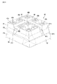
次に、液晶表示装置10について詳細に説明する。図2は、液晶表示装置の斜視図、図3は、液晶表示装置の分解斜視図、図4Aは、図2の線X1−X1に沿った液晶表示装置の断面図、図4Bは、図2の線Y1−Y1に沿ったリフレクタおよび光源ユニットの断面図である。
図2および図3に示すように、液晶表示装置10は、アクティブマトリクス型の液晶表示パネル12と、液晶表示パネル12の背面に対向して設けられた照明装置(バックライト装置)30と、液晶表示パネル12の表示面12aが露出した状態で、液晶表示パネル12およびバックライト装置30を収納した外ケース50と、を備えている。バックライト装置30は、液晶表示パネル12に背面側から光を照射して照明する。
Next, the liquid
As shown in FIGS. 2 and 3, the liquid
液晶表示パネル12は、矩形平板状の第1基板SUB1と、第1基板SUB1に対向配置された矩形平板状の第2基板SUB2と、第1基板SUB1と第2基板SUB2との間に保持された液晶層LQと、を備えている。第1基板SUB1および第2基板SUB2は、例えば、ガラス基板のような絶縁基板を用いている。第1基板SUB1と第2基板SUB2は、これらの間に所定のセルギャップを形成した状態で枠状のシール材SEによって貼り合わされている。液晶層LQは、セルギャップにおいてシール材SEによって囲まれた内側に保持されている。
The liquid
平面視でシール材SEの内側となる領域に、画像を表示する表示領域(アクティブ領域)DAが設けられている。液晶表示パネル12は、表示領域DAにマトリクス状に配列された複数の画素PXを備えている。図3に概略的に示すように、第1基板SUB1は、表示領域DAにおいて、第1方向に延出するゲート線G、第2方向に延出するソース線S、各画素PXにおいてゲート線Gおよびソース線Sと電気的に接続されたスイッチング素子SW、各画素PXにおいてスイッチング素子SWに接続された画素電極PEなどを備えている。コモン電位の共通電極CEは、第1基板SUB1または第2基板SUB2に備えられ、複数の画素電極PEと対向する。なお、ゲート線Gは第1方向に平行な直線状に形成されていなくても良いし、ソース線Sは第2方向に平行な直線状に形成されていなくても良い。
A display area (active area) DA for displaying an image is provided in a region inside the sealing material SE in a plan view. The liquid
図示した例では、第1基板SUB1の短辺側の端部は、第2基板SUB2の短辺よりも外側に突出し、この端部に駆動素子としての駆動IC14が実装されている。また、第1基板SUB1の端部に、フレキシブルプリント回路基板(FPC)16が接合され、液晶表示パネル12から外方に延出している。FPC16は、第1基板SUB1上の配線を介して駆動IC14に接続されている。駆動IC14は、図示しないコントローラからFPC16を介して送られる映像信号および走査信号に基づいて、画素PXに駆動信号を供給する。
In the illustrated example, the end portion on the short side side of the first substrate SUB1 projects outward from the short side of the second substrate SUB2, and the
液晶表示パネル12は、バックライト装置30からの光を表示領域DAに選択的に透過させることで画像を表示する透過表示機能を備えている。液晶表示パネル12は、主として基板主面に略平行な電界を利用する横電界モードに対応した構成としても良いし、主として基板主面に略垂直な電界を利用する縦電界モードに対応した構成としても良い。
The liquid
次に、バックライト装置30の構成例を詳細に説明する。図2および図3に示すように、バックライト装置30は、複数の光源を有する光源ユニット(光源部)32と、光源ユニット32と液晶表示パネル12との間に設けられたリフレクタ40と、液晶表示パネル12とリフレクタ40との間に設けられた光学シート、例えば、拡散シートOSと、を備えている。リフレクタ40は、光源ユニット32から出射された光を反射しながら指向性を持って液晶表示パネル12に投射する。なお、図において、液晶表示パネル12およびバックライト装置30の長手方向をX軸方向、幅方向をY軸方向、高さ方向をZ軸方向としている。
Next, a configuration example of the
図4Aは、図2の線X1−X1に沿ったバックライト装置30の一部の断面図、図4Bは、図2の線Y1−Y1に沿ったリフレクタの断面図である。図3および図4Aに示すように、光源ユニット32は、矩形状の回路基板34と、この回路基板34上に実装された光源として、複数の発光ダイオード(LED)36と、を有している。回路基板34は、液晶表示パネル12とほぼ等しい寸法(長さ、幅)に形成されている。例えば、32個のLED36が回路基板34上に実装され、縦4列、横8列にマトリクス状に配置されている。各LED36は、円形、矩形、楕円形等、種々の形状に形成可能である。一例では、各LED36は、矩形状に形成されている。各LED36の上面は発光面36aを構成し、この発光面36aの中央に発光中心Cを有している。複数のLED36は、その一辺が他のLEDの一辺と整列するように配置されている。なお、LED36の設置数および配列は、上記一例に限らず、液晶表示パネル12の寸法、形状に応じて、種々変更可能である。
回路基板34は、フレキシブルプリント回路基板(FPC)38を介して、図示しないコントローラに接続される。複数のLED36は、コントローラにより、それぞれ独立して点灯駆動される。すなわち、複数のLED36は、同時に全点灯可能であるとともに、表示画像に応じて幾つかのLEDを部分的に点灯するローカルディミング駆動することができる。
4A is a cross-sectional view of a part of the
The
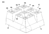
図5は、リフレクタの出射面側の一部を示す斜視図、図6は、リフレクタの入射面側の一部を示す斜視図である。
図3ないし図6に示すように、リフレクタ40は、液晶表示パネル12とほぼ等しい大きさを有する矩形枠状の外壁42と、外壁42の内側に格子状にクロスして配置された複数の隔壁(側壁)44とを有している。リフレクタ40は、例えば、白色の合成樹脂(例えば、ポリエチレンテレフタレート)により一体成形されている。リフレクタ40は、出射面40aとなる上面と、入射面40bとなる底面とを有している。出射面40aは、液晶表示パネル12とほぼ等しい大きさの矩形状を成している。
FIG. 5 is a perspective view showing a part of the reflector on the exit surface side, and FIG. 6 is a perspective view showing a part of the reflector on the incident surface side.
As shown in FIGS. 3 to 6, the
出射面40aには、外壁42および複数の側壁44により規定された複数の出射開口46aが開口している。一例では、各出射開口46aは、4辺を有する矩形状あるいは正方形に形成されている。そして、複数の出射開口46aは、出射面40aの長手方向(X軸方向)および幅方向(Y軸方向)に隣接して並んでいる。本実施形態において、LED36の数に合わせて、32個の出射開口46aが設けられ、縦4列、横8列に並んでいる。
入射面40bには、外壁42および複数の側壁44により規定された複数の入射開口46bが開口している。各入射開口46bは、4辺を有する矩形状あるいは正方形に形成されている。LED36の数に合わせて、32個の出射開口46aが設けられ、縦4列、横8列に並んでいる。また、各入射開口46bは、出射開口46aよりも十分に小さい寸法、例えば、1/2以下の寸法に形成されている。各入射開口46bは、対応する出射開口46aと同軸の位置に設けられている。
A plurality of
A plurality of
リフレクタ40は、側壁44の両面および外壁42の内面で形成された複数の反射面48を有している。すなわち、反射面48は、それぞれの出射開口46aごとに4面ずつ設けられている。各反射面48は、入射開口46bの一辺から出射開口46aの一辺まで延びている。各反射面48は、複数の曲面を組み合わせた面で構成されている。本実施形態では、各反射面48は、入射開口46bの1辺からリフレクタ40の高さ方向の中途部まで延びる第1曲面48aと、中途部から出射開口46aの1辺まで延びる第2曲面48bと、を有している。第1曲面48aは、例えば、出射開口46aの中心を通る中心軸Z1あるいはLED36の光軸C1に対して、凸となる曲面であり、第2曲面48bは、中心軸Z1あるいは光軸C1に対して、凹となる曲面としている。
なお、本実施形態で用いる曲面とは、リフレクタの出射面40aあるいは液晶表示パネル12と平行な直線状の中心軸を有する曲面であり、球面を含まないものとしている。
The
The curved surface used in the present embodiment is a curved surface having a linear central axis parallel to the
図4Aおよび図4Bに示すように、本実施形態では、X軸方向に対向する2つの反射面48と、Y軸方向に対向する2つの反射面48とは、曲面の曲率を相違させている。例えば、X軸方向に対向する2つの反射面48において、第1曲面48aおよび第2曲面48bは曲率半径R1、R2であり、R1≧R2としている。Y軸方向に対向する2つの反射面48において、第1曲面48aおよび第2曲面48bは曲率半径R3、R4であり、R3≧R4、R3≧R1としている。
第1曲面48aおよび第2曲面48bの曲率半径R1〜R4は、それぞれ反射効率を考慮して適宜設定する。例えば、LED36から出射された光を強い指向性を持って液晶表示パネル12側に反射するように、また、出射開口46aの全体から均一に光が出射するように、第1曲面48aおよび第2曲面48bの曲率半径を選択する。
As shown in FIGS. 4A and 4B, in the present embodiment, the curvatures of the curved surfaces of the two reflecting
The radii of curvature R1 to R4 of the first
図4A、図4B、図5に示すように、リフレクタ40の外壁42および側壁44の出射面40a側端部において、各出射開口46aの4つの角部は、所定の深さで切りかかれ、凹所51を形成している。このような凹所51を設けることにより、出射開口46aの角部での光の干渉を抑制し、角部における輝度の低下を防止している。
As shown in FIGS. 4A, 4B, and 5, at the
図3および図4Aに示すように、リフレクタ40は、弾性シートあるいはクッションシート52を介して、回路基板34上に載置されている。弾性材で形成されたクッションシート52は、回路基板34とほぼ等しい大きさの矩形状に形成されている。クッションシート52には、それぞれLED36を収容する複数の透孔54が形成されている。各透孔54は、LED36よりも大きな矩形状に形成されている。
リフレクタ40は、入射面40bがクッションシート52上に載置されている。リフレクタ40は、各出射開口46aの中心軸Z1がLED36の光軸C1と同芯に位置した状態で、クッションシート52上に載置されている。これにより、LED36は、リフレクタ40の入射開口46b内に位置している。
このような弾性シートあるいはクッションシート52の弾性変形により回路基板34あるいはリフレクタ40の歪を吸収することができ、回路基板34およびLED36に対してリフレクタ40を適正な位置に保持することができる。また、弾性シートあるいはクッションシート52により、LED36および回路基板34の熱をリフレクタ40に伝熱し、リフレクタ40から放熱することができる。
クッションシート52の表面または構成部材を高反射率とすることで、回路基板34または回路基板34とリフレクタ40との隙間へ向かう光をリフレクタ40へ向かわせることができ、LED36から出射した光を効率良くリフレクタ40内へ入射させることができる。また、クッションシート52の表面または構成部材を光透過率が低いものとすることで、回路基板34または回路基板34とリフレクタ40との隙間からの光漏れを低減することができる。
As shown in FIGS. 3 and 4A, the
The
The elastic deformation of the elastic sheet or
By setting the surface or the constituent members of the
図2、図3、図4Aに示すように、リフレクタ40の出射面40aは、所定の隙間を置いて、液晶表示パネル12の背面に対向している。この出射面40aと液晶表示パネル12との間に拡散シートOSが配置されている。拡散シートOSは、隙間d(例えば、2mm)をおいて、リフレクタ40の出射面40aと対向している。
As shown in FIGS. 2, 3 and 4A, the
以上のように構成された液晶表示装置10によれば、LED36から出射された光の一部は、直接、リフレクタ40の出射開口46aを通り、拡散シートOSに入射する。また、光の他の部分は、リフレクタ40の反射面48により反射され、出射開口46aを通して拡散シートOSに入射する。このように、LED36から出射された光は、リフレクタ40の出射開口46aから指向性を持って拡散シートOSに入射し、更に、この拡散シートOSを通して液晶表示パネル12に投射される。
According to the liquid
図7は、LED36の目標輝度プロファイルを示している。このようなLED36とリフレクタ40とを組み合わせた場合、図8に示すように、各出射開口46aから出射する光の単独転動輝度分布BIを隣同士で複数組み合わせることにより、全域に亘って均一な他点灯輝度分布BCが得られる。
FIG. 7 shows the target brightness profile of the
各出射開口46aに繋がる反射面48を曲率半径の異なる第1曲面48aと第2曲面48bとを組み合わせて構成することにより、更に、本実施形態によれば、矩形状の出射開口46aの4辺に繋がる4面の反射面48を設けることにより、点光源であるLED36から出射されたランバーシアン出光を、リフレクタ40により四角錐台状の出光プロファイルに変換することが可能となる。図9は、リフレクタ40の出光プロファイルの一例を示している。
By forming the reflecting
また、バックライト装置30のLED36を2Dローカルディミング駆動(エリア分割駆動)することにより、液晶表示装置10の消費電力の低減を図ることができる。ローカルディミング駆動では、外壁42および側壁44によりLED36毎に分割されたリフレクタ40を用いて、個々のLED36を点灯制御することで、液晶表示パネル12の必要な分割エリアだけに光を照射し、すなわち、画像表示する領域のみに光を照射し、シャープな画像を表示することができる。同時に、光源ユニット32の発熱量の低減を図ることが可能となる。また、点灯-非点灯エリアがリフレクタ40の側壁44(反射面48)で仕切られているため、コントラストの高い2Dローカルディミング駆動となる。
以上のことから、本実施形態によれば、高い指向性を有し高輝度化が可能な照明装置および表示装置を得ることができる。
なお、上述した第1の実施形態において、リフレクタ40の反射面を構成する曲面は、2つに限らず、3つ以上の曲面を組み合わせて構成してもよい。出射開口は矩形に限らず、3角形あるいは5角形以上の多角形としてもよい。また、出射開口に繋がる反射面は、4面に限らず、3面あるいは5面以上とすることが可能である。更に、反射率を上げる目的で、反射面上に金属蒸着膜を形成してもよい。リフレクタ40は、合成樹脂に限らず、金属材料で形成してもよい。
Further, by driving the
From the above, according to the present embodiment, it is possible to obtain a lighting device and a display device having high directivity and capable of increasing brightness.
In the first embodiment described above, the curved surface forming the reflection surface of the
次に、他の実施形態に係る表示装置のリフレクタについて説明する。以下に説明する他の実施形態において、前述した第1の実施形態と同一の部分には、同一の参照符号を付してその詳細な説明を省略あるいは簡略化し、第1の実施形態と異なる部分を中心に詳しく説明する。 Next, the reflector of the display device according to another embodiment will be described. In other embodiments described below, the same parts as those in the first embodiment described above are designated by the same reference numerals to omit or simplify the detailed description thereof, and parts different from those in the first embodiment. Will be explained in detail.
(第2の実施形態)
図10は、第2の実施形態に係る表示装置におけるリフレクタおよび光源ユニットの平面図、図11は、図10の線X2−X2に沿ったリフレクタおよび光源ユニットの断面図、図12は、図10の線Y2−Y2に沿ったリフレクタおよび光源ユニットの断面図である。
図10ないし図12に示すように、第2の実施形態によれば、液晶表示装置のリフレクタ40は、出射面に設けられた複数の矩形状の出射開口46aと、入射面に設けられた複数の矩形状の出射開口46aと、側壁44の両面および外壁42の内面で形成された複数の反射面48と、を有している。反射面48は、それぞれの出射開口46aごとに4面ずつ設けられている。各反射面48は、入射開口46bの一辺から出射開口46aの一辺まで延びている。各反射面48は、複数の曲面を組み合わせた面で構成されている。本実施形態では、各反射面48は、入射開口46bの1辺からリフレクタ40の高さ方向の中途部まで延びる第1曲面48aと、中途部から出射開口46aの1辺まで延びる第2曲面48bと、を有している。第1曲面48aは、例えば、出射開口46aの中心を通る中心軸Z1あるいはLED36の光軸C1に対して、凹となる曲面であり、第2曲面48bは、中心軸Z1あるいは光軸C1に対して、凹となる曲面としている。
(Second embodiment)
10 is a plan view of the reflector and the light source unit in the display device according to the second embodiment, FIG. 11 is a cross-sectional view of the reflector and the light source unit along the line X2-X2 of FIG. 10, and FIG. 12 is FIG. It is sectional drawing of the reflector and the light source unit along the line Y2-Y2 of.
As shown in FIGS. 10 to 12, according to the second embodiment, the
図11および図12に示すように、本実施形態では、X軸方向に対向する2つの反射面48と、Y軸方向に対向する2つの反射面48とは、曲面の曲率を相違させている。例えば、X軸方向に対向する2つの反射面48において、第1曲面48aおよび第2曲面48bは曲率半径R1、R2であり、R1≦R2としている。Y軸方向に対向する2つの反射面48において、第1曲面48aおよび第2曲面48bは曲率半径R3、R4であり、R3≦R4、R3≦R1としている。
第1曲面48aおよび第2曲面48bの曲率半径R1〜R4は、それぞれ反射効率を考慮して適宜設定する。すなわち、LED36から出射された光を強い指向性を持って液晶表示パネル12側に反射するように、また、出射開口46aの全体から均一に光が出射するように、第1曲面48aおよび第2曲面48bの曲率半径を選択する。
第2の実施形態において、バックライト装置および液晶表示装置の他の構成は、前述した第1の実施形態と同様である。
As shown in FIGS. 11 and 12, in the present embodiment, the two reflecting
The radii of curvature R1 to R4 of the first
In the second embodiment, the other configurations of the backlight device and the liquid crystal display device are the same as those in the first embodiment described above.
以上のように構成された第2の実施形態によれば、各出射開口46aに繋がる反射面48を曲率半径の異なる第1曲面48aと第2曲面48bとを組み合わせて構成することにより、更に、矩形状の出射開口46aの4辺に繋がる4面の反射面48を設けることにより、点光源であるLED36から出射されたランバーシアン出光を、リフレクタ40により四角錐台状の出光プロファイルに変換することが可能となる。図13は、リフレクタ40の出光プロファイルの一例を示している。その他、第2の実施形態においても、第1の実施形態と同様の作用効果を得ることができる。
According to the second embodiment configured as described above, the reflecting
(第3の実施形態)
図14は、第3の実施形態に係る表示装置におけるリフレクタおよび光源ユニットの平面図、図15は、図14の線X3−X3に沿ったリフレクタおよび光源ユニットの断面図、図16は、図14の線Y3−Y3に沿ったリフレクタおよび光源ユニットの断面図である。
図14ないし図16に示すように、第3の実施形態によれば、リフレクタ40の反射面48は、それぞれの出射開口46aごとに4面ずつ設けられている。各反射面48は、入射開口46bの一辺から出射開口46aの一辺まで延びている。各反射面48は、複数の曲面を組み合わせた面で構成されている。本実施形態では、各反射面48は、入射開口46bの1辺からリフレクタ40の高さ方向の中途部まで延びる第1曲面48aと、中途部から出射開口46aの1辺まで延びる第2曲面48bと、を有している。第1曲面48aは、出射開口46aの中心軸Z1あるいはLED36の光軸C1に対して、凸となる曲面であり、第2曲面48bは、中心軸Z1あるいは光軸C1に対して、凸となる曲面としている。
(Third Embodiment)
14 is a plan view of the reflector and the light source unit in the display device according to the third embodiment, FIG. 15 is a cross-sectional view of the reflector and the light source unit along the line X3-X3 of FIG. 14, and FIG. 16 is FIG. It is sectional drawing of the reflector and the light source unit along the line Y3-Y3 of.
As shown in FIGS. 14 to 16, according to the third embodiment, four reflecting
図15および図16に示すように、X軸方向に対向する2つの反射面48と、Y軸方向に対向する2つの反射面48とは、曲面の曲率を相違させている。例えば、X軸方向に対向する2つの反射面48において、第1曲面48aおよび第2曲面48bは曲率半径R1、R2であり、R1≧R2としている。Y軸方向に対向する2つの反射面48において、第1曲面48aおよび第2曲面48bは曲率半径R3、R4であり、R3≧R4、R3≦R1としている。
第1曲面48aおよび第2曲面48bの曲率半径R1〜R4は、LED36から出射された光を強い指向性を持って液晶表示パネル12側に反射するように、また、出射開口46aの全体から均一に光が出射するように、第1曲面48aおよび第2曲面48bの曲率半径を選択している。
第3の実施形態において、バックライト装置および液晶表示装置の他の構成は、前述した第1の実施形態と同様である。
As shown in FIGS. 15 and 16, the two reflecting
The radii of curvature R1 to R4 of the first
In the third embodiment, the other configurations of the backlight device and the liquid crystal display device are the same as those in the first embodiment described above.
以上のように構成された第3の実施形態によれば、各出射開口46aに繋がる反射面48を曲率半径の異なる第1曲面48aと第2曲面48bとを組み合わせて構成することにより、更に、矩形状の出射開口46aの4辺に繋がる4面の反射面48を設けることにより、点光源であるLED36から出射されたランバーシアン出光を、リフレクタ40により四角錐台状の出光プロファイルに変換することが可能となる。図17は、リフレクタ40の出光プロファイルの一例を示している。その他、第3の実施形態においても、前述した第1の実施形態と同様の作用効果を得ることができる。
第3の実施形態によれば、第1曲面48aは曲率半径R2とR4とを有し、第2曲面48bは曲率半径R1とR3とを有するので、曲率半径の異なる曲面をつなぎ合わせた境界480は、図14に示すように曲線となる。
なお、上述した第2の実施形態および第3の実施形態において、前述した第1の実施形態と同様に、各出射開口46aの4つの角部に凹所を形成してもよい。
According to the third embodiment configured as described above, the reflecting
According to the third embodiment, the first
In the second embodiment and the third embodiment described above, recesses may be formed at the four corners of each exit opening 46a as in the first embodiment described above.
(第4の実施形態)
図18は、第4の実施形態に係る表示装置におけるリフレクタおよび光源ユニットの平面図、図19は、図18の線X4−X4に沿ったリフレクタおよび光源ユニットの断面図、図20は、図18の線Y4−Y4に沿ったリフレクタおよび光源ユニットの断面図である。
バックライト装置のリフレクタは、高さを高くするほど(光の通過距離を長くするほど)、その指向性が向上する。また、リフレクタの内壁に、すなわち、反射面に、アルミニウム等の金属膜を蒸着することで反射率は向上する。しかし、リフレクタの高さ(深さ)が増すと、反射面に均一な金属膜を形成することが困難となる。
そこで、本実施形態では、リフレクタ40を高さ方向(中心軸Z1の軸方向)に複数に分割し、個々の分割ブロックの内壁に蒸着膜を形成した後、これらの分割ブロックを互いに接合して一体化することにより、リフレクタ40を構成している。
(Fourth Embodiment)
FIG. 18 is a plan view of the reflector and the light source unit in the display device according to the fourth embodiment, FIG. 19 is a sectional view of the reflector and the light source unit along the line X4-X4 of FIG. It is sectional drawing of the reflector and the light source unit along the line Y4-Y4 of.
The higher the height of the reflector of the backlight device (the longer the light passing distance), the better the directivity of the reflector. Further, the reflectance is improved by depositing a metal film such as aluminum on the inner wall of the reflector, that is, on the reflective surface. However, as the height (depth) of the reflector increases, it becomes difficult to form a uniform metal film on the reflecting surface.
Therefore, in the present embodiment, the
詳細に述べると、図18ないし図20に示すように、バックライト装置のリフレクタ40は、出射面に設けられた複数の矩形状の出射開口46aと、入射面に設けられた複数の矩形状の出射開口46aと、側壁44の両面および外壁42の内面で形成された複数の反射面48と、を有している。反射面48は、それぞれの出射開口46aごとに4面ずつ設けられている。反射面48は、入射開口46bの一辺から出射開口46aの一辺まで延びている。各反射面48は、複数の曲面を組み合わせた面で構成されている。本実施形態では、反射面48は、入射開口46bの1辺からリフレクタ40の高さ方向の中途部まで延びる第1曲面48aと、中途部から出射開口46aの1辺まで延びる第2曲面48bと、を有している。第1曲面48aは、例えば、出射開口46aの中心を通る中心軸Z1あるいはLED36の光軸C1に対して、凹となる曲面であり、第2曲面48bは、中心軸Z1あるいは光軸C1に対して、凹となる曲面としている。
More specifically, as shown in FIGS. 18 to 20, the
図19および図20に示すように、本実施形態では、X軸方向に対向する2つの反射面48と、Y軸方向に対向する2つの反射面48とは、曲面の曲率を相違させている。例えば、X軸方向に対向する2つの反射面48において、第1曲面48aおよび第2曲面48bは曲率半径R1、R2であり、R1≦R2としている。Y軸方向に対向する2つの反射面48において、第1曲面48aおよび第2曲面48bは曲率半径R3、R4であり、R3≦R4、R3≦R1としている。
第1曲面48aおよび第2曲面48bの曲率半径R1〜R4は、それぞれ反射効率を考慮して適宜設定する。すなわち、LED36から出射された光を強い指向性を持って液晶表示パネル12側に反射するように、また、出射開口46aの全体から均一に光が出射するように、第1曲面48aおよび第2曲面48bの曲率半径を選択する。
As shown in FIGS. 19 and 20, in the present embodiment, the curvatures of the curved surfaces of the two reflecting
The radii of curvature R1 to R4 of the first
本実施形態によれば、図18ないし図20に示すように、リフレクタ40は、高さ方向(中心軸Z1の軸方向)に複数、例えば、3つに分割された第1分割ブロックP1、第2分割ブロックP2、第3分割ブロックP3を有している。分割面は、それぞれ中心軸Z1と交差する、例えば、直交する2つの分割平面DP1、DP2としている。分割平面DP1、DP2は、それぞれ各反射面48を横切っている。第1、第2、第3分割ブロックP1、P2、P3は、白色樹脂等の共通の材料、あるいは、互いに異なる材料でそれぞれ成形されている。反射面48を構成する第1分割ブロックP1の内面、第2分割ブロックP2の内面、および第3分割ブロックP3の内面に、それぞれ蒸着膜(反射膜)60が形成されている。これら第1、第2、第3分割ブロックP1、P2、P3を順に積層し、かつ、互いに接合することにより、一体のリフレクタ40が構成されている。
According to the present embodiment, as shown in FIGS. 18 to 20, the
蒸着膜60は、分割ブロックごとに蒸着材料(反射率)を変えてもよい。例えば、第1分割ブロックP1の蒸着膜60の反射率をA、第2分割ブロックP1の蒸着膜60の反射率をB、第3分割ブロックP3の蒸着膜60の反射率C(A>B>C)としてもよい。すなわち、光源(LED36)側から出射開口46aに向かって、反射面48の反射率が徐々に低下するようにしてもよい。
また、蒸着膜60は、分割ブロックごとに膜厚を変えてもよい。例えば、第1分割ブロックP1の蒸着膜60の膜厚をAH、第2分割ブロックP2の蒸着膜60の膜厚をBH、第3分割ブロックP3の蒸着膜60の膜厚をCHとし、AH<BH<CHとしてもよい。分割ブロックの壁厚は、P1>P2>P2であることから、蒸着膜60の膜厚をAH<BH<CHとすることにより、分割ブロックから隣接分割ブロックへの光漏れを防止することができる。
The
Further, the film thickness of the vapor-deposited
分割ブロックごとに形成材料を変えてもよい。例えば、第1分割ブロックP1を黒色樹脂、第2分割ブロックP2を白色樹脂、第3分割ブロックP3を透明樹脂でそれぞれ形成してもよい。このように、光源(LED36)に近い分割ブロックをより濃色の材料で形成することにより、隣接分割ブロックへの光漏れを防止することができる。また、第1、第2、第3分割ブロックP1、P2、P3は、合成樹脂に限らず、例えば、アルミニウム、銀、窒化シリコン等の異なる材料で形成してもよい。更に、リフレクタ40の外面(表面)に蒸着膜を形成してもよい。この場合、リフレクタの放熱性を向上することができる。
The forming material may be changed for each divided block. For example, the first divided block P1 may be formed of black resin, the second divided block P2 may be formed of white resin, and the third divided block P3 may be formed of transparent resin. In this way, by forming the dividing block close to the light source (LED36) with a darker color material, it is possible to prevent light leakage to the adjacent dividing block. Further, the first, second, and third divided blocks P1, P2, and P3 are not limited to synthetic resins, and may be formed of different materials such as aluminum, silver, and silicon nitride. Further, a thin-film deposition film may be formed on the outer surface (surface) of the
以上のように構成された第4の実施形態によれば、前述した第1の実施形態と同様の作用効果を得ることができる。更に、本実施形態によれば、リフレクタを複数の分割ブロックを接合して構成することにより、リフレクタの高さを高くした場合でも反射面に蒸着膜を容易に形成することができる。各分割ブロックに均一な膜厚の蒸着膜を形成し、安定した反射特性を得ることが可能となる。あるいは、分割ブロック毎に反射面の反射率、膜厚等を変えることが可能であり、リフレクタ40の反射特性を容易に調整可能となる。
According to the fourth embodiment configured as described above, the same effects as those of the first embodiment described above can be obtained. Further, according to the present embodiment, by forming the reflector by joining a plurality of divided blocks, it is possible to easily form a thin-film deposition film on the reflective surface even when the height of the reflector is increased. A vapor-deposited film having a uniform film thickness can be formed on each divided block, and stable reflection characteristics can be obtained. Alternatively, the reflectance, film thickness, and the like of the reflecting surface can be changed for each divided block, and the reflecting characteristics of the
図21および図22は、図4ないし図6に示した反射面48に、曲面の曲率が異なる第1曲面48aおよび第2曲面48bを有するリフレクタ40を3つのブロックに分割した構成例を示している。図18乃至図20と同様に、リフレクタ40は、高さ方向(中心軸Z1の軸方向)に複数、例えば、3つに分割された第1分割ブロックP1、第2分割ブロックP2、第3分割ブロックP3を有している。分割面は、それぞれ中心軸Z1と交差する、例えば、直交する2つの分割平面DP1、DP2としている。分割平面DP1、DP2は、それぞれ各反射面48を横切っている。第1、第2、第3分割ブロックP1、P2、P3は、白色樹脂等の共通の材料、あるいは、互いに異なる材料でそれぞれ成形されている。反射面48を構成する第1分割ブロックP1の内面、第2分割ブロックP2の内面、および第3分割ブロックP3の内面に、それぞれ蒸着膜(反射膜)60が形成されている。これら第1、第2、第3分割ブロックP1、P2、P3を順に積層し、かつ、互いに接合することにより、一体のリフレクタ40が構成されている。
21 and 22 show a configuration example in which the
図21及び図22に示すリフレクタ40では、第1分割ブロックP1にサポート610が形成されている。第1分割ブロックP1が分割平面DP1で分割される場合に、X−Y方向にサポート610で支持されるので第1分割ブロックP1がバラバラになることを防ぐことができる。
なお、上述した第4の実施形態、および図21及び図22に示した構成例において、リフレクタ40は、3つに分割したが、これに限らず、2つ、あるいは4つ以上に分割してもよい。図21及び図22に示すリフレクタ40の第1曲面48aと第2曲面48bとの境界で2つの曲率に分かれているので、リフレクタ40を第1曲面48aと第2曲面48bとの境界で2つに分割することも可能である。
In the
In the fourth embodiment described above and the configuration examples shown in FIGS. 21 and 22, the
本発明の幾つかの実施形態を説明したが、これらの実施形態は、例として提示したものであり、発明の範囲を限定することは意図していない。新規な実施形態は、その他の様々な形態で実施されることが可能であり、発明の要旨を逸脱しない範囲で、種々の省略、置き換え、変更を行うことができる。実施形態やその変形例は、発明の範囲や要旨に含まれるとともに、特許請求の範囲に記載された発明とその均等の範囲に含まれる。 Although some embodiments of the present invention have been described, these embodiments are presented as examples and are not intended to limit the scope of the invention. The novel embodiment can be implemented in various other embodiments, and various omissions, replacements, and changes can be made without departing from the gist of the invention. The embodiments and modifications thereof are included in the scope and gist of the invention, and are included in the scope of the invention described in the claims and the equivalent scope thereof.
本発明の実施形態として上述した各構成を基にして、当業者が適宜設計変更して実施し得る全ての構成も、本発明の要旨を包含する限り、本発明の範囲に属する。例えば、液晶表示パネルおよびバックライト装置の構成部材は、矩形状に限定されることなく、5角形以上の多角形、楕円形、トラック形状等の他の形状としてもよい。また、構成部材の材料および寸法は、上述した例に限らず、種々選択可能である。
上述した実施形態によりもたらされる他の作用効果について本明細書の記載から明らかなもの、又は当業者において適宜想到し得るものついては、当然に本発明によりもたらされるものと解される。
All configurations that can be implemented by those skilled in the art with appropriate design changes based on the configurations described above as embodiments of the present invention also belong to the scope of the present invention as long as the gist of the present invention is included. For example, the constituent members of the liquid crystal display panel and the backlight device are not limited to the rectangular shape, but may have other shapes such as a polygonal shape of pentagon or more, an ellipse shape, and a track shape. Further, the materials and dimensions of the constituent members are not limited to the above-mentioned examples, and various types can be selected.
Other effects brought about by the above-described embodiments that are clear from the description of the present specification, or that can be appropriately conceived by those skilled in the art, are naturally understood to be brought about by the present invention.
10…液晶表示装置、12…液晶表示パネル、30…バックライト装置、
32…光源ユニット、34…回路基板、36…光源(LED)、40…リフレクタ、
42…外壁、44…側壁、46a…出射開口、46b…入射開口、48…反射面、
48a…第1曲面、48b…第2曲面、52…クッションシート、54…凹所
10 ... liquid crystal display device, 12 ... liquid crystal display panel, 30 ... backlight device,
32 ... Light source unit, 34 ... Circuit board, 36 ... Light source (LED), 40 ... Reflector,
42 ... outer wall, 44 ... side wall, 46a ... exit opening, 46b ... incident opening, 48 ... reflective surface,
48a ... 1st curved surface, 48b ... 2nd curved surface, 52 ... Cushion sheet, 54 ... Recess
Claims (10)
前記リフレクタは、それぞれ前記光源部からの光が入射する複数の入射開口と、前記入射開口に対向する複数の出射開口と、前記入射開口から前記出射開口までそれぞれ延在する複数の反射面と、前記反射面に形成された反射膜と、を有し、
前記出射開口は、第1方向に対向する2辺と第2方向に対向する2辺の4辺を有する矩形状を有し、
前記入射開口は、第1方向に対向する2辺と第2方向に対向する2辺の4辺を有する矩形状を有し、
前記反射面は、それぞれ前記出射開口の1辺から前記入射開口の1辺まで延在する曲面を有する4面の反射面を含み、
前記第1方向に対向する反射面の曲率半径は、前記第2方向に対向する反射面の曲率半径と異なり、
前記リフレクタは、複数のブロックを有し、前記複数のブロックは互いに接合されて前記リフレクタを構成している照明装置。 It has a light source unit and a reflector provided so as to face the light source unit.
The reflector includes a plurality of incident openings into which light from the light source unit is incident, a plurality of exit openings facing the incident aperture, and a plurality of reflective surfaces extending from the incident aperture to the exit aperture. It has a reflective film formed on the reflective surface and
The exit opening has a rectangular shape having four sides, two sides facing each other in the first direction and two sides facing each other in the second direction.
The incident aperture has a rectangular shape having four sides, two sides facing each other in the first direction and two sides facing each other in the second direction.
Each of the reflecting surfaces includes four reflecting surfaces having a curved surface extending from one side of the emitting opening to one side of the incident opening.
The radius of curvature of the reflecting surface facing the first direction is different from the radius of curvature of the reflecting surface facing the second direction.
The reflector has a plurality of blocks, and the plurality of blocks are joined to each other to form the reflector.
前記第1ブロックの内面に形成された反射膜の反射率は、前記第2ブロックの内面に形成された反射膜の反射率と相違している請求項2に記載の照明装置。 The plurality of blocks include a first block located on the light source side and a second block laminated on the first block.
The lighting device according to claim 2, wherein the reflectance of the reflective film formed on the inner surface of the first block is different from the reflectance of the reflective film formed on the inner surface of the second block.
前記第1方向に対向する前記反射面の各々は、前記光源の光軸に対して凹となる第1曲面と、前記光源の光軸に対して凹となる第2曲面と、を有し、
前記第2方向に対向する前記反射面の各々は、前記光源の光軸に対して凹となる第3曲面と、前記光軸に対して凹となる第4曲面と、を有し、
前記第1曲面及び前記第3曲面は、前記入射開口側に位置し、
前記第2曲面及び前記第4曲面は、前記出射開口側に位置し、
前記第1曲面および第2曲面は、互いに異なる曲率半径を有し、
前記第3曲面および前記第4曲面は、互いに異なる曲率半径を有し、
前記第1曲面及び前記第3曲面は、互いに異なる曲率半径を有している請求項1から6のいずれか1項に記載の照明装置。 The light source unit has a plurality of light sources and has a plurality of light sources.
Each of the reflecting surfaces facing the first direction has a first curved surface that is concave with respect to the optical axis of the light source and a second curved surface that is concave with respect to the optical axis of the light source.
Each of the reflecting surfaces facing the second direction has a third curved surface that is concave with respect to the optical axis of the light source and a fourth curved surface that is concave with respect to the optical axis.
The first curved surface and the third curved surface are located on the incident opening side.
The second curved surface and the fourth curved surface are located on the exit opening side.
The first curved surface and the second curved surface have different radii of curvature from each other .
The third curved surface and the fourth curved surface have different radii of curvature from each other.
The lighting device according to any one of claims 1 to 6, wherein the first curved surface and the third curved surface have different radii of curvature from each other.
前記第1方向に対向する前記反射面の各々は、前記光源の光軸に対して凸となる第1曲面と、前記光源の光軸に対して凹となる第2曲面と、を有し、
前記第2方向に対向する前記反射面の各々は、前記光源の光軸に対して凸となる第3曲面と、前記光軸に対して凹となる第4曲面と、を有し、
前記第1曲面及び前記第3曲面は、前記入射開口側に位置し、
前記第2曲面及び前記第4曲面は、前記出射開口側に位置し、
前記第1曲面および第2曲面は、互いに異なる曲率半径を有し、
前記第3曲面および前記第4曲面は、互いに異なる曲率半径を有し、
前記第1曲面及び前記第3曲面は、互いに異なる曲率半径を有している請求項1から6のいずれか1項に記載の照明装置。 The light source unit has a plurality of light sources and has a plurality of light sources.
Each of the reflecting surfaces facing the first direction has a first curved surface that is convex with respect to the optical axis of the light source and a second curved surface that is concave with respect to the optical axis of the light source.
Each of the reflecting surfaces facing the second direction has a third curved surface that is convex with respect to the optical axis of the light source and a fourth curved surface that is concave with respect to the optical axis.
The first curved surface and the third curved surface are located on the incident opening side.
The second curved surface and the fourth curved surface are located on the exit opening side.
The first curved surface and the second curved surface have different radii of curvature from each other .
The third curved surface and the fourth curved surface have different radii of curvature from each other.
The lighting device according to any one of claims 1 to 6, wherein the first curved surface and the third curved surface have different radii of curvature from each other.
前記第1方向に対向する前記反射面の各々は、前記光源の光軸に対して凸となる第1曲面と、前記光源の光軸に対して凸となる第2曲面と、を有し、
前記第2方向に対向する前記反射面の各々は、前記光源の光軸に対して凸となる第3曲面と、前記光軸に対して凸となる第4曲面と、を有し、
前記第1曲面及び前記第3曲面は、前記入射開口側に位置し、
前記第2曲面及び前記第4曲面は、前記出射開口側に位置し、
前記第1曲面および第2曲面は、互いに異なる曲率半径を有し、
前記第3曲面および前記第4曲面は、互いに異なる曲率半径を有し、
前記第1曲面及び前記第3曲面は、互いに異なる曲率半径を有している請求項1から6のいずれか1項に記載の照明装置。 The light source unit has a plurality of light sources and has a plurality of light sources.
Each of the reflecting surfaces facing the first direction has a first curved surface that is convex with respect to the optical axis of the light source and a second curved surface that is convex with respect to the optical axis of the light source.
Each of the reflecting surfaces facing the second direction has a third curved surface that is convex with respect to the optical axis of the light source and a fourth curved surface that is convex with respect to the optical axis.
The first curved surface and the third curved surface are located on the incident opening side.
The second curved surface and the fourth curved surface are located on the exit opening side.
The first curved surface and the second curved surface have different radii of curvature from each other .
The third curved surface and the fourth curved surface have different radii of curvature from each other.
The lighting device according to any one of claims 1 to 6, wherein the first curved surface and the third curved surface have different radii of curvature from each other.
前記リフレクタは、前記各出射開口の各角部において、前記外壁および隔壁に形成された複数の凹所を有している請求項1から9のいずれか1項に記載の照明装置。The lighting device according to any one of claims 1 to 9, wherein the reflector has a plurality of recesses formed in the outer wall and the partition wall at each corner of each exit opening.
Priority Applications (7)
| Application Number | Priority Date | Filing Date | Title |
|---|---|---|---|
| JP2017015809A JP6906968B2 (en) | 2017-01-31 | 2017-01-31 | Lighting device |
| US15/881,917 US10216036B2 (en) | 2017-01-31 | 2018-01-29 | Illumination device |
| US16/242,166 US10514575B2 (en) | 2017-01-31 | 2019-01-08 | Illumination device for use in local dimming |
| US16/539,371 US11061275B2 (en) | 2017-01-31 | 2019-08-13 | Illumination device for use in local dimming |
| US17/342,990 US11385499B2 (en) | 2017-01-31 | 2021-06-09 | Illumination device for use in local dimming |
| JP2021106588A JP7135166B2 (en) | 2017-01-31 | 2021-06-28 | Reflector, head-up display with reflector, and vehicle equipped with head-up display |
| US17/834,290 US11573455B2 (en) | 2017-01-31 | 2022-06-07 | Illumination device for use in local dimming |
Applications Claiming Priority (1)
| Application Number | Priority Date | Filing Date | Title |
|---|---|---|---|
| JP2017015809A JP6906968B2 (en) | 2017-01-31 | 2017-01-31 | Lighting device |
Related Child Applications (1)
| Application Number | Title | Priority Date | Filing Date |
|---|---|---|---|
| JP2021106588A Division JP7135166B2 (en) | 2017-01-31 | 2021-06-28 | Reflector, head-up display with reflector, and vehicle equipped with head-up display |
Publications (2)
| Publication Number | Publication Date |
|---|---|
| JP2018125137A JP2018125137A (en) | 2018-08-09 |
| JP6906968B2 true JP6906968B2 (en) | 2021-07-21 |
Family
ID=62979761
Family Applications (2)
| Application Number | Title | Priority Date | Filing Date |
|---|---|---|---|
| JP2017015809A Active JP6906968B2 (en) | 2017-01-31 | 2017-01-31 | Lighting device |
| JP2021106588A Active JP7135166B2 (en) | 2017-01-31 | 2021-06-28 | Reflector, head-up display with reflector, and vehicle equipped with head-up display |
Family Applications After (1)
| Application Number | Title | Priority Date | Filing Date |
|---|---|---|---|
| JP2021106588A Active JP7135166B2 (en) | 2017-01-31 | 2021-06-28 | Reflector, head-up display with reflector, and vehicle equipped with head-up display |
Country Status (2)
| Country | Link |
|---|---|
| US (5) | US10216036B2 (en) |
| JP (2) | JP6906968B2 (en) |
Families Citing this family (13)
| Publication number | Priority date | Publication date | Assignee | Title |
|---|---|---|---|---|
| WO2018017436A1 (en) | 2016-07-22 | 2018-01-25 | President And Fellows Of Harvard College | Controls optimization for wearable systems |
| JP6906968B2 (en) | 2017-01-31 | 2021-07-21 | 株式会社ジャパンディスプレイ | Lighting device |
| JP7214317B2 (en) * | 2019-02-13 | 2023-01-30 | マレリ株式会社 | Backlight device for head-up display |
| JP7433866B2 (en) * | 2019-11-28 | 2024-02-20 | キヤノン株式会社 | Sheet conveyance device and image reading device |
| JP7441069B2 (en) | 2020-02-18 | 2024-02-29 | シャープ株式会社 | backlight device |
| WO2021166807A1 (en) * | 2020-02-21 | 2021-08-26 | ソニーグループ株式会社 | Light source device and image display device |
| JP7032680B1 (en) | 2020-08-28 | 2022-03-09 | 日亜化学工業株式会社 | Light emitting device |
| US11281047B1 (en) * | 2020-12-01 | 2022-03-22 | Solomon Systech (China) Limited | Backlight generation with local dimming for liquid crystal panel having arbitrary shape |
| KR20220139587A (en) * | 2021-04-08 | 2022-10-17 | 현대모비스 주식회사 | Head-Up Display Device |
| US11868005B2 (en) | 2021-06-15 | 2024-01-09 | Nichia Corporation | Partitioning member, planar light source, and liquid crystal display device |
| CN113359352B (en) * | 2021-07-01 | 2022-09-20 | 业成科技(成都)有限公司 | Direct type backlight module and display thereof |
| JP2023016089A (en) * | 2021-07-21 | 2023-02-02 | 株式会社ジャパンディスプレイ | Lighting device |
| JP2023037174A (en) * | 2021-09-03 | 2023-03-15 | 株式会社ジャパンディスプレイ | Lighting device |
Family Cites Families (18)
| Publication number | Priority date | Publication date | Assignee | Title |
|---|---|---|---|---|
| US6871982B2 (en) | 2003-01-24 | 2005-03-29 | Digital Optics International Corporation | High-density illumination system |
| KR100987545B1 (en) * | 2005-11-29 | 2010-10-12 | 쇼와 덴코 가부시키가이샤 | Reflector frame, flat light source device provided with the reflector frame, and display device using the flat light source device |
| KR101220204B1 (en) * | 2005-12-28 | 2013-01-09 | 엘지디스플레이 주식회사 | Light Emitting Diodes back-light assembly and liquid crystal display device module using thereof |
| KR20070079649A (en) * | 2006-02-03 | 2007-08-08 | 삼성전자주식회사 | Backlight assembly and display device having the same |
| JP4720694B2 (en) | 2006-09-14 | 2011-07-13 | 株式会社デンソー | Vehicle display device |
| JP2010092672A (en) * | 2008-10-06 | 2010-04-22 | Harison Toshiba Lighting Corp | Backlight device, and display device |
| TW201017052A (en) * | 2008-10-27 | 2010-05-01 | Delta Electronics Inc | Illuminant device and light reflecting shade thereof |
| JP2011060488A (en) * | 2009-09-08 | 2011-03-24 | Kazuhisa Genma | Lighting device |
| US9494823B2 (en) * | 2012-07-12 | 2016-11-15 | Samsung Display Co., Ltd. | Method and apparatus for achieving uniform high locality light |
| WO2014014134A1 (en) * | 2012-07-17 | 2014-01-23 | 엘지전자 주식회사 | Display device |
| JP6072817B2 (en) * | 2012-11-01 | 2017-02-01 | 日立マクセル株式会社 | Light source device and projection display device |
| JP2014202835A (en) | 2013-04-03 | 2014-10-27 | 三菱電機株式会社 | Illumination device and image display device |
| CN105976725B (en) * | 2016-06-20 | 2019-04-02 | 深圳市华星光电技术有限公司 | Micro- LED display panel |
| JP6906968B2 (en) * | 2017-01-31 | 2021-07-21 | 株式会社ジャパンディスプレイ | Lighting device |
| JP2019061128A (en) * | 2017-09-27 | 2019-04-18 | 株式会社ジャパンディスプレイ | Display device and head-up display device |
| JP2019101056A (en) * | 2017-11-28 | 2019-06-24 | 株式会社ジャパンディスプレイ | Display device and head-up display device |
| US11281084B2 (en) * | 2018-07-18 | 2022-03-22 | Optonomous Technologies, Inc. | Illumination system with crystal phosphor mechanism and method of operation thereof |
| JP2020134250A (en) * | 2019-02-15 | 2020-08-31 | 株式会社キーエンス | Image processing device |
-
2017
- 2017-01-31 JP JP2017015809A patent/JP6906968B2/en active Active
-
2018
- 2018-01-29 US US15/881,917 patent/US10216036B2/en active Active
-
2019
- 2019-01-08 US US16/242,166 patent/US10514575B2/en active Active
- 2019-08-13 US US16/539,371 patent/US11061275B2/en active Active
-
2021
- 2021-06-09 US US17/342,990 patent/US11385499B2/en active Active
- 2021-06-28 JP JP2021106588A patent/JP7135166B2/en active Active
-
2022
- 2022-06-07 US US17/834,290 patent/US11573455B2/en active Active
Also Published As
| Publication number | Publication date |
|---|---|
| US11061275B2 (en) | 2021-07-13 |
| JP2018125137A (en) | 2018-08-09 |
| US10514575B2 (en) | 2019-12-24 |
| US20180217448A1 (en) | 2018-08-02 |
| JP2021180179A (en) | 2021-11-18 |
| US10216036B2 (en) | 2019-02-26 |
| US11573455B2 (en) | 2023-02-07 |
| US20220299822A1 (en) | 2022-09-22 |
| US20210294161A1 (en) | 2021-09-23 |
| US20190361298A1 (en) | 2019-11-28 |
| US11385499B2 (en) | 2022-07-12 |
| JP7135166B2 (en) | 2022-09-12 |
| US20190137824A1 (en) | 2019-05-09 |
Similar Documents
| Publication | Publication Date | Title |
|---|---|---|
| JP6776140B2 (en) | Lighting device | |
| JP6906968B2 (en) | Lighting device | |
| US11294173B2 (en) | Display device and head-up display device | |
| US8714804B2 (en) | Backlight assembly and display apparatus having the same | |
| US9291820B2 (en) | Display module and head up display | |
| US11841582B2 (en) | Display device | |
| JP2021517351A (en) | Lighting device | |
| KR101940946B1 (en) | Head-up display device | |
| JP6995958B2 (en) | Lighting equipment | |
| US20230041447A1 (en) | Head Up Display Apparatus With a Bright Energy Efficient Backlight for a Vehicle | |
| US9052542B2 (en) | Light source package and backlight unit including the light source package | |
| KR20100010861A (en) | Liquid crystal display device | |
| US20180045961A1 (en) | Head Up Display Device | |
| KR102548363B1 (en) | Head-Up display |
Legal Events
| Date | Code | Title | Description |
|---|---|---|---|
| A621 | Written request for application examination |
Free format text: JAPANESE INTERMEDIATE CODE: A621 Effective date: 20191125 |
|
| A977 | Report on retrieval |
Free format text: JAPANESE INTERMEDIATE CODE: A971007 Effective date: 20201029 |
|
| A131 | Notification of reasons for refusal |
Free format text: JAPANESE INTERMEDIATE CODE: A131 Effective date: 20201104 |
|
| A521 | Request for written amendment filed |
Free format text: JAPANESE INTERMEDIATE CODE: A523 Effective date: 20201223 |
|
| TRDD | Decision of grant or rejection written | ||
| A01 | Written decision to grant a patent or to grant a registration (utility model) |
Free format text: JAPANESE INTERMEDIATE CODE: A01 Effective date: 20210601 |
|
| A61 | First payment of annual fees (during grant procedure) |
Free format text: JAPANESE INTERMEDIATE CODE: A61 Effective date: 20210630 |
|
| R150 | Certificate of patent or registration of utility model |
Ref document number: 6906968 Country of ref document: JP Free format text: JAPANESE INTERMEDIATE CODE: R150 |