JP6892827B2 - Free-form nanostructured surfaces for virtual reality and augmented reality near-eye displays - Google Patents
Free-form nanostructured surfaces for virtual reality and augmented reality near-eye displays Download PDFInfo
- Publication number
- JP6892827B2 JP6892827B2 JP2017551633A JP2017551633A JP6892827B2 JP 6892827 B2 JP6892827 B2 JP 6892827B2 JP 2017551633 A JP2017551633 A JP 2017551633A JP 2017551633 A JP2017551633 A JP 2017551633A JP 6892827 B2 JP6892827 B2 JP 6892827B2
- Authority
- JP
- Japan
- Prior art keywords
- eye display
- display assembly
- meta
- combiner
- assembly according
- Prior art date
- Legal status (The legal status is an assumption and is not a legal conclusion. Google has not performed a legal analysis and makes no representation as to the accuracy of the status listed.)
- Active
Links
- 230000003190 augmentative effect Effects 0.000 title description 4
- 230000003287 optical effect Effects 0.000 claims description 22
- 230000004075 alteration Effects 0.000 claims description 6
- 238000001228 spectrum Methods 0.000 claims description 5
- 238000001429 visible spectrum Methods 0.000 claims description 5
- 238000004519 manufacturing process Methods 0.000 description 8
- 230000000694 effects Effects 0.000 description 6
- 230000010287 polarization Effects 0.000 description 5
- 238000012937 correction Methods 0.000 description 4
- 230000000737 periodic effect Effects 0.000 description 4
- 230000004044 response Effects 0.000 description 4
- 230000005540 biological transmission Effects 0.000 description 3
- 210000003128 head Anatomy 0.000 description 3
- 230000000712 assembly Effects 0.000 description 2
- 238000000429 assembly Methods 0.000 description 2
- 230000001419 dependent effect Effects 0.000 description 2
- 230000005684 electric field Effects 0.000 description 2
- 239000004973 liquid crystal related substance Substances 0.000 description 2
- 210000001747 pupil Anatomy 0.000 description 2
- 239000000758 substrate Substances 0.000 description 2
- 230000001174 ascending effect Effects 0.000 description 1
- 230000007423 decrease Effects 0.000 description 1
- 229910003460 diamond Inorganic materials 0.000 description 1
- 239000010432 diamond Substances 0.000 description 1
- 210000005069 ears Anatomy 0.000 description 1
- 238000005286 illumination Methods 0.000 description 1
- 238000003384 imaging method Methods 0.000 description 1
- 230000001678 irradiating effect Effects 0.000 description 1
- ORUIBWPALBXDOA-UHFFFAOYSA-L magnesium fluoride Chemical compound [F-].[F-].[Mg+2] ORUIBWPALBXDOA-UHFFFAOYSA-L 0.000 description 1
- 229910001635 magnesium fluoride Inorganic materials 0.000 description 1
- 229910052751 metal Inorganic materials 0.000 description 1
- 239000002184 metal Substances 0.000 description 1
- 238000003801 milling Methods 0.000 description 1
- 238000012986 modification Methods 0.000 description 1
- 230000004048 modification Effects 0.000 description 1
- 239000002086 nanomaterial Substances 0.000 description 1
- 238000012545 processing Methods 0.000 description 1
- 230000001681 protective effect Effects 0.000 description 1
- 229910052710 silicon Inorganic materials 0.000 description 1
- 239000010703 silicon Substances 0.000 description 1
- 229910052709 silver Inorganic materials 0.000 description 1
- 239000004332 silver Substances 0.000 description 1
- 238000004088 simulation Methods 0.000 description 1
- 230000003595 spectral effect Effects 0.000 description 1
- 238000002834 transmittance Methods 0.000 description 1
Images


Classifications
-
- G—PHYSICS
- G02—OPTICS
- G02B—OPTICAL ELEMENTS, SYSTEMS OR APPARATUS
- G02B27/00—Optical systems or apparatus not provided for by any of the groups G02B1/00 - G02B26/00, G02B30/00
- G02B27/01—Head-up displays
- G02B27/017—Head mounted
- G02B27/0172—Head mounted characterised by optical features
-
- G—PHYSICS
- G02—OPTICS
- G02B—OPTICAL ELEMENTS, SYSTEMS OR APPARATUS
- G02B27/00—Optical systems or apparatus not provided for by any of the groups G02B1/00 - G02B26/00, G02B30/00
- G02B27/10—Beam splitting or combining systems
- G02B27/1066—Beam splitting or combining systems for enhancing image performance, like resolution, pixel numbers, dual magnifications or dynamic range, by tiling, slicing or overlapping fields of view
-
- G—PHYSICS
- G02—OPTICS
- G02B—OPTICAL ELEMENTS, SYSTEMS OR APPARATUS
- G02B6/00—Light guides; Structural details of arrangements comprising light guides and other optical elements, e.g. couplings
- G02B6/0001—Light guides; Structural details of arrangements comprising light guides and other optical elements, e.g. couplings specially adapted for lighting devices or systems
- G02B6/0011—Light guides; Structural details of arrangements comprising light guides and other optical elements, e.g. couplings specially adapted for lighting devices or systems the light guides being planar or of plate-like form
- G02B6/0013—Means for improving the coupling-in of light from the light source into the light guide
- G02B6/0015—Means for improving the coupling-in of light from the light source into the light guide provided on the surface of the light guide or in the bulk of it
- G02B6/0016—Grooves, prisms, gratings, scattering particles or rough surfaces
-
- G—PHYSICS
- G02—OPTICS
- G02B—OPTICAL ELEMENTS, SYSTEMS OR APPARATUS
- G02B6/00—Light guides; Structural details of arrangements comprising light guides and other optical elements, e.g. couplings
- G02B6/0001—Light guides; Structural details of arrangements comprising light guides and other optical elements, e.g. couplings specially adapted for lighting devices or systems
- G02B6/0011—Light guides; Structural details of arrangements comprising light guides and other optical elements, e.g. couplings specially adapted for lighting devices or systems the light guides being planar or of plate-like form
- G02B6/0033—Means for improving the coupling-out of light from the light guide
- G02B6/0035—Means for improving the coupling-out of light from the light guide provided on the surface of the light guide or in the bulk of it
- G02B6/0038—Linear indentations or grooves, e.g. arc-shaped grooves or meandering grooves, extending over the full length or width of the light guide
-
- G—PHYSICS
- G02—OPTICS
- G02B—OPTICAL ELEMENTS, SYSTEMS OR APPARATUS
- G02B27/00—Optical systems or apparatus not provided for by any of the groups G02B1/00 - G02B26/00, G02B30/00
- G02B27/01—Head-up displays
- G02B27/0101—Head-up displays characterised by optical features
- G02B2027/011—Head-up displays characterised by optical features comprising device for correcting geometrical aberrations, distortion
-
- G—PHYSICS
- G02—OPTICS
- G02B—OPTICAL ELEMENTS, SYSTEMS OR APPARATUS
- G02B27/00—Optical systems or apparatus not provided for by any of the groups G02B1/00 - G02B26/00, G02B30/00
- G02B27/01—Head-up displays
- G02B27/0101—Head-up displays characterised by optical features
- G02B2027/0123—Head-up displays characterised by optical features comprising devices increasing the field of view
- G02B2027/0125—Field-of-view increase by wavefront division
-
- G—PHYSICS
- G02—OPTICS
- G02B—OPTICAL ELEMENTS, SYSTEMS OR APPARATUS
- G02B27/00—Optical systems or apparatus not provided for by any of the groups G02B1/00 - G02B26/00, G02B30/00
- G02B27/01—Head-up displays
- G02B27/017—Head mounted
- G02B27/0172—Head mounted characterised by optical features
- G02B2027/0174—Head mounted characterised by optical features holographic
-
- G—PHYSICS
- G02—OPTICS
- G02B—OPTICAL ELEMENTS, SYSTEMS OR APPARATUS
- G02B27/00—Optical systems or apparatus not provided for by any of the groups G02B1/00 - G02B26/00, G02B30/00
- G02B27/01—Head-up displays
- G02B27/017—Head mounted
- G02B2027/0178—Eyeglass type
-
- G—PHYSICS
- G02—OPTICS
- G02B—OPTICAL ELEMENTS, SYSTEMS OR APPARATUS
- G02B5/00—Optical elements other than lenses
- G02B5/18—Diffraction gratings
- G02B5/1809—Diffraction gratings with pitch less than or comparable to the wavelength
-
- G—PHYSICS
- G02—OPTICS
- G02B—OPTICAL ELEMENTS, SYSTEMS OR APPARATUS
- G02B5/00—Optical elements other than lenses
- G02B5/18—Diffraction gratings
- G02B5/1814—Diffraction gratings structurally combined with one or more further optical elements, e.g. lenses, mirrors, prisms or other diffraction gratings
-
- G—PHYSICS
- G02—OPTICS
- G02B—OPTICAL ELEMENTS, SYSTEMS OR APPARATUS
- G02B5/00—Optical elements other than lenses
- G02B5/18—Diffraction gratings
- G02B5/1876—Diffractive Fresnel lenses; Zone plates; Kinoforms
-
- H—ELECTRICITY
- H04—ELECTRIC COMMUNICATION TECHNIQUE
- H04N—PICTORIAL COMMUNICATION, e.g. TELEVISION
- H04N13/00—Stereoscopic video systems; Multi-view video systems; Details thereof
- H04N13/30—Image reproducers
- H04N13/332—Displays for viewing with the aid of special glasses or head-mounted displays [HMD]
- H04N13/344—Displays for viewing with the aid of special glasses or head-mounted displays [HMD] with head-mounted left-right displays
-
- H—ELECTRICITY
- H04—ELECTRIC COMMUNICATION TECHNIQUE
- H04N—PICTORIAL COMMUNICATION, e.g. TELEVISION
- H04N9/00—Details of colour television systems
- H04N9/12—Picture reproducers
- H04N9/31—Projection devices for colour picture display, e.g. using electronic spatial light modulators [ESLM]
- H04N9/3129—Projection devices for colour picture display, e.g. using electronic spatial light modulators [ESLM] scanning a light beam on the display screen
Description
本発明は、仮想現実および拡張現実ニアアイディスプレイ用の自由形状ナノ構造面に関する。 The present invention relates to free-form nanostructured surfaces for virtual reality and augmented reality near-eye displays.
ニアアイディスプレイは、ユーザの視界の前に表示を生じるウェアラブルデバイスである。このディスプレイは透明または不透明であり得る。例えば、透明なディスプレイは、現実世界の視界の上に情報およびグラフィックをオーバーレイするものであり得、一方、不透明なディスプレイは、観察者に対して、ニアアイディスプレイからの情報のみを呈示する。 A near-eye display is a wearable device that produces a display in front of the user's field of view. This display can be transparent or opaque. For example, a transparent display can overlay information and graphics on top of a real-world field of view, while an opaque display presents the observer only with information from the near-eye display.
本明細書に示される態様によれば、画像源と、画像源に光学的に結合されたコンバイナ、二次ミラー、および導波路のうちの少なくとも1つとを含むニアアイディスプレイアセンブリであって、コンバイナ、二次ミラー、および導波路のうちの少なくとも1つが、複数のメタ原子を有する単位セルによって少なくとも部分的に画成されたメタ回折格子を有する自由形状ナノ構造面を含む、ニアアイディスプレイアセンブリが提供される。 According to aspects set forth herein, a near-eye display assembly comprising an image source and at least one of a combiner, a secondary mirror, and a waveguide optically coupled to the image source, the combiner. Near-eye display assemblies that include, at least one of the secondary mirrors, and waveguides, a free-form nanostructured surface with a meta-diffraction grating that is at least partially defined by a unit cell with multiple meta-atoms. Provided.
本明細書に示される更なる態様によれば、画像源に動作可能に接続されたコンバイナおよび二次ミラーのうちの少なくとも1つを有するニアアイディスプレイであって、コンバイナおよび二次ミラーのうちの少なくとも1つが自由形状ナノ構造面を含み、更に、自由形状ナノ構造面が、自由形状面、ナノ構造面、または自由形状面とナノ構造面との組合せを包含する、ニアアイディスプレイが提供される。 According to a further aspect set forth herein, a near-eye display having at least one of a combiner and a secondary mirror operably connected to an image source, the combiner and the secondary mirror. Near-eye displays are provided in which at least one comprises a free-form nanostructured surface, and the free-form nanostructured surface further comprises a free-shaped surface, a nanostructured surface, or a combination of a free-shaped surface and a nanostructured surface. ..
本明細書に示される更なる態様によれば、コンバイナと、コンバイナに動作可能に接続された二次ミラーとを有するニアアイディスプレイであって、コンバイナおよび二次ミラーのうちの少なくとも一方が、複数のメタ原子を有する単位セルによって少なくとも部分的に画成されたメタ回折格子を含む、ニアアイディスプレイが提供される。 According to a further aspect set forth herein, a near-eye display having a combiner and a secondary mirror operably connected to the combiner, wherein at least one of the combiner and the secondary mirror is plural. A near-eye display is provided that includes a meta-diffraction grating that is at least partially defined by a unit cell having a meta-atom of.
別の態様によれば、装着者の頭部に解除可能に係合するフレームと、フレームに動作可能に接続されたコンバイナと、コンバイナおよびフレームのうちの一方に動作可能に接続された二次ミラーとを有するニアアイディスプレイアセンブリであって、コンバイナおよび二次ミラーのうちの少なくとも一方が、複数のメタ原子を有する単位セルによって少なくとも部分的に画成されたメタ回折格子を有する自由形状ナノ構造面を含み、単位セル内のメタ原子がそれぞれ異なる長さ対幅の比率を有すると共に、可視光スペクトルの大部分にわたって少なくとも50%の効率を提供するサイズおよび間隔を有する、ニアアイディスプレイアセンブリが提供される。 According to another aspect, a frame operably engaged to the wearer's head, a combiner operably connected to the frame, and a secondary mirror operably connected to one of the combiner and the frame. Near-eye display assembly with and at least one of the combiner and secondary mirror has a free-form nanostructured surface with a meta-diffraction grating at least partially defined by a unit cell with multiple meta-atoms. Near-eye display assemblies are provided that include, each metaatom in a unit cell has a different length-to-width ratio, and have a size and spacing that provides at least 50% efficiency over most of the visible light spectrum. To.
別の態様において、画像源と、画像源に光学的に結合された導波路とを有するニアアイディスプレイアセンブリであって、導波路が、複数のメタ原子を有する単位セルによって少なくとも部分的に画成されたメタ回折格子を有する自由形状ナノ構造面を含む、ニアアイディスプレイアセンブリが提供される。 In another embodiment, a near-eye display assembly having an image source and a waveguide optically coupled to the image source, wherein the waveguide is at least partially defined by a unit cell having multiple metaatoms. A near-eye display assembly is provided that includes a free-form nanostructured surface with a meta-diffraction grating.
更なる態様によれば、フレームと、フレームに第1の反射面として動作可能に接続されたコンバイナと、フレームに第2の反射面として動作可能に接続された二次ミラーとを有するニアアイディスプレイアセンブリであって、コンバイナおよび二次ミラーの各々が自由形状ナノ構造面を含み、その下の表面形状が自由形状であってもよく、表面上に重ねられたナノ構造が自由形状面を生じてもよく、またはそれらの組合せであってもよく、自由形状特性が、第1の反射面および第2の反射面の傾きおよび芯ずれによって生じる光学収差を補正するよう構成された、ニアアイディスプレイアセンブリが提供される。 According to a further aspect, a near-eye display having a frame, a combiner operably connected to the frame as a first reflective surface, and a secondary mirror operably connected to the frame as a second reflective surface. In the assembly, each of the combiner and the secondary mirror may include a free-form nanostructured surface, and the surface shape beneath it may be free-shaped, and the nanostructures superimposed on the surface give rise to a free-shaped nanostructured surface. A near-eye display assembly in which the free-form properties are configured to correct for optical aberrations caused by tilting and misalignment of the first and second reflective surfaces. Is provided.
ニアアイディスプレイは、観察者に対して、観察瞳(「アイボックス」とも称する)内に画像情報を呈示し、この画像情報は、観察者の目の瞳と位置合わせされた際に、観察者の視野内にバーチャル画像を生じる。ニアアイディスプレイのコンバイナ、または導波路は、観察者の視野の外の位置から観察者の目に向かって画像情報を運ぶ。コンバイナ(または導波路)によって運ばれる画像情報は、バーチャル画像を観察者の目の中に投影するための角度的に符号化された形態を有し得る。 The near-eye display presents image information to the observer in the observation pupil (also referred to as the "eye box"), and this image information is displayed to the observer when aligned with the pupil of the observer's eyes. Produces a virtual image in the field of view of. The near-eye display combiner, or waveguide, carries image information from a position outside the observer's field of view toward the observer's eyes. The image information carried by the combiner (or waveguide) can have an angle-coded form for projecting a virtual image into the observer's eyes.
コンバイナは、コンバイナの同じ側(反射/反射、または透過/透過)からの、またはコンバイナの異なる2つの側からの(反射/透過)2つの画像を合成する光学装置である。コンバイナは、ユーザが、外部の景色に重ねられたコンピュータ生成画像(CGI)を見ることを可能にするヘッドアップディスプレイ(HUD)(ヘッドマウントディスプレイ(HMD)と称される場合もある)またはニアアイディスプレイにおいて用いられ得る。HUDは、ユーザが通常の視点から目をそらさずにCGIを見ることを可能にする。 A combiner is an optical device that synthesizes two images from the same side of the combiner (reflection / reflection or transmission / transmission) or from two different sides of the combiner (reflection / transmission). The combiner is a head-up display (HUD) (sometimes referred to as a head-mounted display (HMD)) or near-eye that allows the user to see a computer-generated image (CGI) superimposed on the outside landscape. Can be used in displays. The HUD allows the user to see the CGI without looking away from the normal point of view.
一般的に、コンバイナには2つのバージョンがある。第1のバージョンは、2つの視野を、どちらの視野にもいかなるレンズ効果も加えずに、合成する(例えば、傾いたダイクロイックプレート等)。第2のバージョンは、合成機能に加えて、ディスプレイから入射する視野に対するレンズ効果機能(これが、全球面、軸外し円錐、非球面、または自由形状のレンズ効果であり得る)を含む。レンズ効果機能は、ディスプレイから発するバーチャル画像を遠視野またはコンバイナからの特定の距離に変位させるため、および、ユーザがターゲットのサイズにおいてバーチャル画像に焦点を合わせるのを可能にするために画像に特定の視野を与えるために用いられる。レンズ効果機能は、表示される視野を通して光学収差の適切な補正を提供するよう構成される。また、レンズ効果機能は、個々のユーザに対して眼科的な補正を提供するよう構成されてもよい。 In general, there are two versions of the combiner. The first version combines the two fields of view without adding any lens effect to either field of view (eg, tilted dichroic plate, etc.). The second version includes, in addition to the compositing function, a lens effect function on the field of view incident from the display, which can be a spherical, off-axis cone, aspherical, or free-form lens effect. The lens effect feature is specific to the image to displace the virtual image emanating from the display to a specific distance from the far field or combiner, and to allow the user to focus on the virtual image at the size of the target. Used to give a field of view. The lens effect function is configured to provide appropriate correction of optical aberrations throughout the displayed field of view. The lens effect function may also be configured to provide ophthalmologic corrections to individual users.
導波路(導光板と称する場合もある)としては、回折型、ホログラフィ式、偏向型、または反射型の導波路が挙げられるが、それらに限定されない。ナノ構造面の態様は、光を導波路に入るようおよび/または導波路から出るよう結合するために用いられ得る。 The waveguide (sometimes referred to as a light guide plate) includes, but is not limited to, a diffraction type, a holographic type, a deflection type, or a reflection type waveguide. Aspects of nanostructured surfaces can be used to couple light into and / or exit the waveguide.
画像情報は、観察者の視野の外から(例えば、眼鏡フレームのテンプルに沿って等)発せられる。電子ビデオ表示データは、空間的パターンを角度的に変形する結像光学系と組み合わされた空間光変調器を含むが、それに限定されない画像源または生成器(例えば、光学パターン生成器等)によって、または、空間的パターンの角度的変形を直接生成する走査光学系によって、画像情報に変換される。画像源は、光のパターンを生成またはコンバイナに伝達する任意の装置を包含する。画像源は、例えば、発光ダイオード(LED)および垂直キャビティ面発光レーザ(VCSEL)に基づくレーザ走査画像源生成器等であるがそれに限定されない画像生成器、並びに、液晶ディスプレイ、反射型もしくは透過型ディスプレイ、および有機発光ダイオード(OLED)を含むがそれらに限定されないマイクロディスプレイを含み、マイクロディスプレイは、光学収差を制御するために走査光路内にまたはマイクロディスプレイに近接してまたは接して配置されるアナモルフィックまたは自由形状の光学要素またはレンズと組み合され得る。二軸対称を有する非対称面は、アナモルフィック面と称される。二軸対称またはトロイダル形状の範囲を超えて非対称な非対称面は、自由形状面である。従って、画像源は、例えばOLEDディスプレイ等の発光型マイクロディスプレイ、および/または、例えばLCoS(液晶オンシリコン)ディスプレイまたはDLP(デジタル光処理)装置等の反射型マイクロディスプレイを含み得る。特定の態様では、表示される各色の光について別々のマイクロディスプレイが用いられてもよく、一方、他の態様では、(例えば、フィールドシーケンシャルカラー方式の画像を表示することによって)単一のマイクロディスプレイが用いられてもよい。同様に、一部の態様では、観察者の左目および右目に対して別々の画像源が用いられてもよい。これは、立体視画像の表示を容易にし得る。そのような態様では、左目用の画像および右目用の別々の画像を生じるために、別々のコンバイナが用いられ得る。 The image information is emitted from outside the observer's field of view (eg, along the temples of the spectacle frame). The electronic video display data includes, but is not limited to, a spatial light modulator combined with an imaging optical system that angularly transforms the spatial pattern, by an image source or generator (eg, an optical pattern generator, etc.). Alternatively, it is converted into image information by a scanning optical system that directly generates angular deformations of the spatial pattern. The image source includes any device that produces or transmits a pattern of light to the combiner. Image sources include, but are not limited to, light emitting diodes (LEDs) and laser scanning image source generators based on vertical cavity surface emitting lasers (VCSEL), as well as liquid crystal displays, reflective or transmissive displays. , And microdisplays, including but not limited to organic light emitting diodes (OLEDs), the microdisplays being placed in the scanning path or in close proximity to or in contact with the microdisplays to control optical aberrations. It can be combined with a fic or free-form optic or lens. An asymmetric plane with biaxial symmetry is called an anamorphic plane. An asymmetric surface that is biaxially symmetric or asymmetric beyond the toroidal shape is a free-form surface. Thus, the image source may include, for example, a light emitting microdisplay such as an OLED display and / or a reflective microdisplay such as an LCos (liquid crystal on silicon) display or a DLP (digital light processing) device. In certain embodiments, a separate microdisplay may be used for each color of light displayed, while in other embodiments a single microdisplay (eg, by displaying a field sequential color image). May be used. Similarly, in some embodiments, separate image sources may be used for the observer's left and right eyes. This can facilitate the display of stereoscopic images. In such an embodiment, separate combiners may be used to produce an image for the left eye and a separate image for the right eye.
コンバイナ(または導波路)は、観察者の頭部に装着され得る眼鏡に動作可能に接続され得る。眼鏡は、耳に掛けられる左右のテンプルと、鼻に掛けられるノーズピースとを有するフレームを含む。フレームは、各光コンバイナ(または導波路)を、それぞれが対応する観察者の目の前に配置する形状およびサイズを有する。他の形状を有する他のフレーム(例えば、耳アームおよび鼻梁支持部を有するバイザー、単一の連続したヘッドセット部材、ヘッドバンド、ゴーグル型の眼鏡類等)が用いられてもよいことが理解されよう。眼鏡という用語は、補正レンズ、サングラス、保護レンズ、レンズを有するまたは有しないフレーム、補正レンズを有するまたは有しないフレーム、並びに、ニアアイディスプレイを観察者の視野内に動作可能に配置して保持するための他のヘッドマウントを含む。従って、眼鏡は、二次ミラーをコンバイナの近位にまたはコンバイナから離間して配置し得る。 The combiner (or waveguide) may be operably connected to spectacles that can be worn on the observer's head. The spectacles include a frame with left and right temples that hang on the ears and a nosepiece that hangs on the nose. The frame has a shape and size in which each optical combiner (or waveguide) is placed in front of the corresponding observer. It is understood that other frames with other shapes (eg, visors with ear arms and nasal bridge supports, single continuous headset members, headbands, goggle-shaped eyeglasses, etc.) may be used. Yeah. The term spectacles operably positions and holds a correction lens, sunglasses, a protective lens, a frame with or without a lens, a frame with or without a correction lens, and a near-eye display in the observer's field of view. Includes other head mounts for. Therefore, the spectacles may place the secondary mirror proximal to the combiner or away from the combiner.
コンバイナ(または導波路)は、眼鏡レンズの代わりに、またはそれに加えて、観察者の目の前のニアアイディスプレイの厚さを最小化する形態で、フレームに動作可能に接続されて、観察者の視野の外からの画像情報を観察者の視野内に運んでもよい。コンバイナは、眼鏡レンズが眼鏡フレーム内に通常保持される空間に対応する限られた体積の空間を占める。即ち、コンバイナは、従来の眼鏡類の寸法により近くなるように、厚さ(即ち、深さ)が制限され得る、光が跳ね返る面であり得る。導波路は、平坦であっても、または湾曲していてもよく、光を導波路に結合する自由形状ナノ構造面を有する。 The combiner (or waveguide) is operably connected to the frame in place of or in addition to the spectacle lens, in a form that minimizes the thickness of the near-eye display in front of the observer. Image information from outside the field of view of the observer may be carried into the field of view of the observer. The combiner occupies a limited volume of space corresponding to the space normally held in the spectacle frame by the spectacle lens. That is, the combiner can be a light bounce surface whose thickness (ie, depth) can be limited to be closer to the dimensions of conventional eyeglasses. The waveguide may be flat or curved and has free-form nanostructured surfaces that couple light to the waveguide.
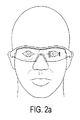
図1〜図4には、ナノ構造面を含む、二次自由形状ミラーを伴うコンバイナと、画像源とを組み込んだニアアイディスプレイアセンブリが示されている。図1〜図4は、ニアアイディスプレイの様々な形状を示しており、図1aおよび図1bのベース形状、図2aおよび図2bの、コンバイナを有するベース形状、図3aおよび図3bの、自由形状ミラーが鼻に近接して配置されている形状、並びに、図4aおよび図4bの、自由形状ミラーが共形であるニアアイディスプレイの形状を含む。図1では、画像源はコンバイナおよび二次ミラーに光学的に結合されている。1つの態様において、コンバイナ、二次ミラー、および画像源は、接続する光路の折り曲げ配置を画成する。更なる態様では、必要に応じて、例えば、球面、非球面、アナモルフィック、アナモルフィック非球面、または自由形状の光学部品またはレンズ等であるがそれらに限定されない光学要素が、画像源と自由形状ナノ構造ミラー、導波路、またはコンバイナとの間に介在し得る。 1 to 4 show a near-eye display assembly incorporating a combiner with a secondary free-form mirror, including nanostructured surfaces, and an image source. 1 to 4 show various shapes of the near-eye display, the base shape of FIGS. 1a and 1b, the base shape having a combiner of FIGS. 2a and 2b, and the free shape of FIGS. 3a and 3b. It includes the shape in which the mirror is placed close to the nose, and the shape of the near-eye display of FIGS. 4a and 4b in which the free-form mirror is conformal. In FIG. 1, the image source is optically coupled to a combiner and a secondary mirror. In one embodiment, the combiner, secondary mirror, and image source define a bent arrangement of connecting optical paths. In a further aspect, an optical element, such as, but not limited to, a spherical surface, an aspherical surface, an anamorphic, an anamorphic aspherical surface, or a free-form optical component or lens, may be used as an image source. It can intervene between free-form nanostructured mirrors, waveguides, or combiners.
ニアアイディスプレイは、2つの反射面、コンバイナ、および二次ミラーを含み得るものであり、コンバイナおよび二次ミラーは軸外し折り曲げ配置にある。1つの態様において、コンバイナおよび二次ミラーの各々は、自由形状ナノ構造面を含む。別の態様において、コンバイナおよび二次ミラーの両方は、自由形状面、ナノ構造面、または自由形状面とナノ構造面との組合せを含み得る。 A near-eye display may include two reflective surfaces, a combiner, and a secondary mirror, the combiner and the secondary mirror being in an off-axis bent arrangement. In one embodiment, each of the combiner and the secondary mirror comprises a free-form nanostructured surface. In another embodiment, both the combiner and the secondary mirror may include a free-form surface, a nanostructured surface, or a combination of a free-shaped surface and a nanostructured surface.
ニアアイディスプレイは、例えば、画像源生成器の光路内のレンズ等であるがそれに限定されない更なる光学部品を含んでもよいことが理解されよう。レンズまたは更なる光学部品は、全球面、非球面、アナモルフィック、アナモルフィック非球面、もしくは自由形状であってもよく、または、全球面、非球面、アナモルフィック、アナモルフィック非球面もしくは自由形状の組合せであってもよい。 It will be appreciated that the near-eye display may include additional optics, such as, but not limited to, a lens in the optical path of the image source generator. The lens or additional optics may be spherical, aspheric, anamorphic, anamorphic aspheric, or free-form, or spherical, aspheric, anamorphic, anamorphic aspheric. Alternatively, it may be a combination of free shapes.
自由形状ナノ構造面の、自由形状面、ナノ構造面、または自由形状面とナノ構造面との組合せの様々な組合せとしての特定の態様を説明する目的で、ニアアイディスプレイアセンブリの複数の態様を述べるが、コンバイナおよび二次ミラーは、それぞれ独立して、自由形状面、ナノ構造面、または自由形状面とナノ構造面との組合せとしての自由形状ナノ構造面を有するよう構成されてもよいことが理解されよう。 A plurality of aspects of a near-eye display assembly are described for the purpose of describing specific aspects of free-form nanostructured surfaces as various combinations of free-shaped surfaces, nanostructured surfaces, or combinations of free-shaped and nanostructured surfaces. As described above, the combiner and the secondary mirror may be configured to independently have a free-form surface, a nanostructured surface, or a free-shaped nanostructured surface as a combination of the free-shaped surface and the nanostructured surface. Will be understood.
一般的に、自由形状面は、折り曲げ配置における反射面の傾きおよび芯ずれによって生じる光学収差を補正するために用いられる。本明細書において用いられる自由形状光学面とは、二軸対称またはトロイダル形状の範囲を超えて非対称な任意の回転非対称面である。自由形状面は、例えば、Φ多項式(例えば、ゼルニケ集合、Q多項式、他の直交多項式の集合、XY多項式、放射基底関数、スプライン、または非一様有理Bスプライン(NURBS)等の正規化された基底関数によってパラメーター化され得る。本明細書において用いられる二軸対称を有する面は、アナモルフィック面と称される。 Generally, the free-form surface is used to correct the optical aberration caused by the tilt and misalignment of the reflective surface in the bent arrangement. As used herein, a free-form optical surface is any rotationally asymmetric surface that is asymmetric beyond the range of biaxial symmetry or toroidal shapes. Free-form planes are normalized, for example, Φ polynomials (eg, Zernike set, Q polynomial, set of other orthogonal polynomials, XY polynomials, radial basis functions, splines, or non-uniform rational B splines (NURBS)). It can be parameterized by basis functions. The biaxially symmetric planes used herein are referred to as anamorphic planes.
ナノ構造面は波面制御を提供する。ナノ構造面は、典型的な特徴が約1〜200nmの範囲内の寸法を有する面または基体である。 Nanostructured surfaces provide wave surface control. A nanostructured surface is a surface or substrate whose typical features have dimensions in the range of about 1-200 nm.
少なくとも1つの選択された態様では、コンバイナおよび二次ミラーの両方は、ナノ構造面としてメタ回折格子を含む。更なる態様では、メタ回折格子は、可視スペクトルにわたって波面を制御する。単位セルの工学的構造および各単位セル内のサブ構造は、一種の自由形状面も生じる。即ち、自由形状面は、メタ回折格子面そのものであってもよく、または、自由形状基体と組み合わされたものであってもよい。 In at least one selected embodiment, both the combiner and the secondary mirror include a meta-diffraction grating as a nanostructured surface. In a further aspect, the meta-diffraction grating controls the wave front over the visible spectrum. The engineering structure of the unit cells and the substructures within each unit cell also give rise to a kind of free-form surface. That is, the free-form plane may be the meta-diffraction grating plane itself, or may be combined with the free-form substrate.
メタ回折格子は複数の単位セルで構成されており、各単位セルは複数のメタ原子を含む。メタ原子のサイズおよび間隔は、少なくとも部分的に、メタ回折格子の動作特性を決定する。1つの態様において、メタ回折格子は、1800線/mmの可視スペクトルメタ回折格子として構成される。 The meta diffraction grating is composed of a plurality of unit cells, and each unit cell contains a plurality of meta atoms. The size and spacing of the metaatoms, at least in part, determine the operating characteristics of the metadiffraction grating. In one embodiment, the meta-diffraction grating is configured as a visible spectrum meta-diffraction grating of 1800 lines / mm.
図5および図6を参照すると、1800線/mmの可視スペクトルメタ回折格子の単位セルが示されている。図5および図6に示されるように、単位セルは4つのメタ原子を含み得る。図5では、メタ原子は、位相が減少する順に1〜4の番号で示されている。 With reference to FIGS. 5 and 6, a unit cell of a visible spectrum meta-diffraction grating of 1800 lines / mm is shown. As shown in FIGS. 5 and 6, the unit cell may contain four metaatoms. In FIG. 5, metaatoms are numbered 1 to 4 in ascending order of phase.
1つの態様において、単位セルは、ベース層、誘電層、およびメタ原子層の3つの層を含む。誘電層はベース層によって支持されており、メタ原子層は誘電層によって支持されている。 In one embodiment, the unit cell comprises three layers: a base layer, a dielectric layer, and a metaatomic layer. The dielectric layer is supported by the base layer and the metaatomic layer is supported by the dielectric layer.
ベース層は、例えば銀等の金属層である。誘電層はフッ化マグネシウムで形成されている。以下の表に示すように、ベース層は約130nmの厚さを有し、誘電層は約75nmの厚さを有する。反射率および透過率の両方を確保するために、メタ回折格子装置には、光がメタ回折格子を透過するのを可能にするアパチャーパターンおよびサイズを有する穿孔が施されている。穿孔は、装置を観察者に対して略透明にするのに十分なものである。 The base layer is, for example, a metal layer such as silver. The dielectric layer is made of magnesium fluoride. As shown in the table below, the base layer has a thickness of about 130 nm and the dielectric layer has a thickness of about 75 nm. To ensure both reflectance and transmittance, the meta-diffraction grating device is perforated with an aperture pattern and size that allows light to pass through the meta-diffraction grating. The perforation is sufficient to make the device substantially transparent to the observer.
1800線/mmの可視スペクトルメタ回折格子の、4つのメタ原子を有する単位セル内のメタ原子の寸法は、以下の表に示されていると共に、図5および図6においてラベルづけされている。 The dimensions of the metaatoms in a unit cell with four metaatoms of a 1800 line / mm visible spectrum metadiffraction grating are shown in the table below and are labeled in FIGS. 5 and 6.

1つの態様において、各メタ原子の各寸法および隣接するメタ原子間の間隔を約10nmより大きく且つ約80nm未満とする単位セルの構成によって、製造時の考慮すべき事項が緩和される。一部の態様では、メタ原子の寸法または隣接するメタ原子間の間隔の最小製造寸法は、約25nmより大きく且つ約60nm未満である。しかし、製造プロセスは、単位セルの構成が約1nmの寸法を含むことを可能にし得ることが理解されよう。 In one embodiment, the configuration of the unit cell in which each dimension of each metaatom and the spacing between adjacent metaatoms is greater than about 10 nm and less than about 80 nm alleviates manufacturing considerations. In some embodiments, the size of the meta atom or the minimum manufacturing size of the spacing between adjacent meta atoms is greater than about 25 nm and less than about 60 nm. However, it will be appreciated that the manufacturing process can allow the unit cell configuration to include dimensions of about 1 nm.
ニアアイディスプレイの軸外し折り曲げ配置において、コンバイナおよび二次ミラーの一方または両方は、自由形状面とナノ構造面(例えば、メタ回折格子等)とを有する自由形状ナノ構造面を含むことが考えられる。 In an off-axis bent arrangement of a near-eye display, one or both of the combiner and the secondary mirror may include a free-form nanostructured surface having a free-shaped surface and a nanostructured surface (eg, a meta-diffraction grating, etc.). ..
図7からわかるように、4つのメタ原子の全ては、575nmより長い波長については、80%より大きい振幅を示す。スペクトル範囲の大部分にわたって、第2、第3、および第4のメタ原子間の位相差は一定である。 As can be seen from FIG. 7, all four metaatoms exhibit an amplitude greater than 80% for wavelengths longer than 575 nm. The phase difference between the second, third, and fourth metaatoms is constant over most of the spectral range.
図8において、実線は、第4のメタ原子を用いた隣接するメタ原子間の理想的な2π/4の位相差をベースラインとして表す。 In FIG. 8, the solid line represents the ideal 2π / 4 phase difference between adjacent meta atoms using the fourth meta atom as the baseline.
メタ回折格子の波長依存効率は、図9の予測された効率と質的に概ね一致する。効率は、個々のメタ原子の効率が高まるにつれて、赤色に向かって高まり、メタ原子間の位相間隔が悪化するより長い波長については低下する。角度依存性は、α=βの条件については、TE偏光された機械刻線回折格子の効率と形状が類似しており、その後に最大値が続く。このことは、原因が、生じた伝搬位相におけるばらつきであることを示唆している。 The wavelength-dependent efficiency of the meta-diffraction grating is qualitatively consistent with the predicted efficiency of FIG. The efficiency increases toward red as the efficiency of individual metaatoms increases, and decreases for longer wavelengths where the phase spacing between metaatomes deteriorates. The angle dependence is similar to the efficiency and shape of the TE-polarized mechanically engraved diffraction grating under the condition of α = β, followed by the maximum value. This suggests that the cause is the variation in the propagation phase that occurred.
図10は、横電場(TE)および横磁場(TM)についての、入射角に対するメタ回折格子および機械刻線回折格子のシミュレーションされたm=+1での絶対回折格子効率のプロットである。プロットに示されている各曲線は、単一の波長についての入射角依存応答を表しており、90°未満の回折角度を生じる入射角のみにわたるものである。このシミュレーションは、周期的な面に入射角αを有する平面波を照射し、次に、反射場を遠視野に投影して回折格子効率を決定することによって行われた。 FIG. 10 is a plot of the absolute grating efficiency at m = + 1 of the meta-diffraction grating and the mechanically engraved grating with respect to the incident angle for the transverse electric field (TE) and the transverse magnetic field (TM). Each curve shown in the plot represents an angle of incidence-dependent response for a single wavelength, spanning only the angle of incidence that produces a diffraction angle of less than 90 °. This simulation was performed by irradiating a periodic surface with a plane wave having an incident angle α, and then projecting a reflection field into a distant field to determine the grating efficiency.
全体的に、メタ回折格子のTE偏光効率は、600nmより長い波長については、機械刻線回折格子のTE偏光効率より高く、500nm〜650nmの波長については、TM偏光効率と対等である。 Overall, the TE polarization efficiency of the meta-diffraction grating is higher than the TE polarization efficiency of the mechanically engraved diffraction grating for wavelengths longer than 600 nm, and is comparable to the TM polarization efficiency for wavelengths from 500 nm to 650 nm.
メタ回折格子は、1800線/mmの機械刻線回折格子と比較して、偏光応答に感度を示す。TM偏光の電場は、メタ原子と揃っていないので、波面変調を生じる共鳴を励起しない。 Meta-diffraction gratings are more sensitive to polarization response than mechanically engraved diffraction gratings of 1800 lines / mm. Since the electric field of TM polarized light is not aligned with the meta atom, it does not excite the resonance that causes wave surface modulation.
図11を参照すると、650nmの照明波長における、約555.5nmの長さおよび上記の表に示したメタ原子を有する単位セルの、入射角の関数としての回折効率が示されている。図11からわかるように、水平方向の点線は約50%の効率を表しており、内側のシェードがついた領域は20°の視野に対応し、外側のシェードがついた領域は60°の視野に対応する。従って、メタ回折格子は、可視光スペクトルの大部分にわたって少なくとも約50%の効率を提供する。メタ回折格子は、例えば50%未満等の所与の所定の効率を提供するよう構成されてもよいことが理解されよう。このように、メタ回折格子は、可視光スペクトルの大部分にわたって少なくとも約20%、30%、40%、または50%の効率を提供し得る。 With reference to FIG. 11, the diffraction efficiency of a unit cell having a length of about 555.5 nm and the metaatoms shown in the table above at an illumination wavelength of 650 nm as a function of the angle of incidence is shown. As can be seen from FIG. 11, the horizontal dotted lines represent an efficiency of about 50%, the inner shaded area corresponds to a 20 ° field of view, and the outer shaded area corresponds to a 60 ° field of view. Corresponds to. Therefore, the meta-diffraction grating provides an efficiency of at least about 50% over most of the visible light spectrum. It will be appreciated that the meta-diffraction grating may be configured to provide a given predetermined efficiency, for example less than 50%. Thus, the meta-diffraction grating can provide at least about 20%, 30%, 40%, or 50% efficiency over most of the visible light spectrum.
1つの態様において、メタ回折格子は、反射における所望の波長において、代替の形状において、約20°から高々80°までわたる動作範囲内において、メタ回折格子に入射する光の入射角の関数として、少なくとも約50%の効率を提供するよう構成される。平均入射角は、単位セルの異なる形状毎に様々であることが理解されよう。 In one embodiment, the meta-diffraction grating is used as a function of the angle of incidence of light incident on the meta-diffraction grating at a desired wavelength in reflection, in an alternative shape, within an operating range ranging from about 20 ° to at most 80 °. It is configured to provide at least about 50% efficiency. It will be appreciated that the average angle of incidence varies for different shapes of unit cells.
自由形状構成要素は、コンパクトな折り曲げ形状において軸から外れている際の、反射面の傾きおよび芯ずれによって生じる光学収差を補正するよう選択される。自由形状面は、例えば、Φ多項式(例えば、ゼルニケ集合、Q多項式、他の直交多項式の集合、XY多項式、放射基底関数、スプライン、またはNURBS等の正規化された基底関数によってパラメーター化され得る。 Free-form components are selected to compensate for optical aberrations caused by tilting and misalignment of the reflective surface when off-axis in a compact bent shape. Free-form planes can be parameterized by, for example, a Φ polynomial (eg, a set of Zernike, a Q polynomial, a set of other orthogonal polynomials, an XY polynomial, a radial basis function, a spline, or a normalized basis function such as NURBS.
図12を参照すると、導波路に対する入力カプラーおよび導波路に対する出力カプラー内にナノ構造面を有する導波路が示されている。 With reference to FIG. 12, a waveguide having a nanostructured surface in the input coupler for the waveguide and the output coupler for the waveguide is shown.
製造においては、ナノ構造面のメタ回折格子は、機械刻線回折格子において問題を生じ得る必要な高さプロファイルの制御および周期制御を、メタ回折格子の製造に用いられる二次元二成分表面制御と置き換えることが見込まれる。上述のように、1800線/mmの可視表面として構成されるメタ回折格子に必要な寸法は、約10nmより大きいものであり得る。必要な寸法が約10nmより大きいことは、製造の助けとなり得るが、製造プロセスが1nm台の寸法の製造を提供できる場合には、ナノ構造面は、少なくとも約1nmの寸法を用いてもよい。 In the manufacture, the nanostructured meta-diffraction grating has the necessary height profile control and periodic control that can cause problems in the mechanically engraved grating, with the two-dimensional two-component surface control used in the manufacture of the meta-diffraction grating. Expected to replace. As mentioned above, the dimensions required for a meta-diffraction grating configured as a visible surface of 1800 lines / mm can be greater than about 10 nm. Although the required dimensions greater than about 10 nm can aid in manufacturing, nanostructured surfaces may use dimensions of at least about 1 nm if the manufacturing process can provide manufacturing with dimensions in the 1 nm range.
自由形状光学面は、例えば、米国カリフォルニア州のSynopsys社のCODE V光学設計ソフトウェア等の市販のソフトウェアを用いて設計され得ると共に、例えば、ダイヤモンド旋盤またはフライス盤上のスローまたはファストツールサーボ等であるがそれらに限定されない市販の設備を用いて製造され得る。また、自由形状面は、製造されたマスター型から成形されてもよい。 The free-form optical surface can be designed using commercially available software such as, for example, CODE V optical design software from Synopsys, California, USA, and is, for example, a slow or fast tool servo on a diamond lathe or milling machine. It can be manufactured using commercially available equipment not limited to them. Further, the free-form surface may be formed from a manufactured master mold.
このように、少なくとも1つの反射面が、自由形状面、ナノ構造面(例えば、上述のメタ回折格子等)、または自由形状面とナノ構造面(例えば、メタ回折格子等)との組合せである、仮想現実または拡張現実ヘッドマウントディスプレイが提供される。従って、自由形状ナノ構造面が、自由形状面、ナノ構造面、または自由形状面とナノ構造面との組合せを包含する態様において、ニアアイディスプレイアセンブリは、コンバイナを含むか、または、コンバイナと、コンバイナに動作可能に接続された二次ミラーとを含み、コンバイナおよび二次ミラーのうちの少なくとも一方は、自由形状ナノ構造面を含む。1つの態様では、コンバイナおよび二次ミラーの両方が自由形状ナノ構造面を含む。 As described above, at least one reflecting surface is a free-shaped surface, a nanostructured surface (for example, the meta diffraction grating described above), or a combination of a free-shaped surface and a nanostructured surface (for example, a meta diffraction grating). , Virtual reality or augmented reality head-mounted displays are provided. Thus, in aspects in which the free-form nanostructured surface comprises a free-shaped surface, a nanostructured surface, or a combination of a free-shaped surface and a nanostructured surface, the near-eye display assembly may include a combiner, or the combiner and the combiner. It includes a secondary mirror operably connected to the combiner, and at least one of the combiner and the secondary mirror includes a free-form nanostructured surface. In one embodiment, both the combiner and the secondary mirror include free-form nanostructured surfaces.
更なる態様では、導波路を有し、導波路内の少なくとも1つ光学面がナノ構造面(例えば、メタ回折格子等)である仮想現実または拡張現実ニアアイディスプレイが提供される。 In a further aspect, a virtual reality or augmented reality near-eye display is provided that has a waveguide and at least one optical surface in the waveguide is a nanostructured surface (eg, a meta-diffraction grating, etc.).
なお、上記および他の特徴および機能、またはそれらの代替の特徴および機能は、他の多くの異なるシステムまたは用途に組み込まれ得る。当業者によって、現時点で予見または予期されない様々な代替、変更、変形、または改良がその後に行われ得るものであり、それらも以下の特許請求の範囲によって包含されることが意図される。 It should be noted that the above and other features and functions, or alternative features and functions thereof, may be incorporated into many other different systems or applications. Various alternatives, changes, modifications, or improvements that are currently foreseen or unexpected by those skilled in the art may subsequently be made, which are also intended to be covered by the claims below.
Claims (19)
前記画像源に光学的に結合されたコンバイナ、ミラー、および導波路のうちの少なくとも1つを含むニアアイディスプレイアセンブリであって、
前記コンバイナ、前記ミラー、および前記導波路のうちの前記少なくとも1つが、各々複数のメタ原子を有する複数の単位セルを配列することによって形成されたメタ回折格子を有するナノ構造面を含み、
前記単位セル内の各前記メタ原子の長さ対幅の比率がそれぞれ異なることを特徴とするニアアイディスプレイアセンブリ。 Image source and
A near-eye display assembly that includes at least one of a combiner, a mirror, and a waveguide that is optically coupled to the image source.
The combiner, the mirror, and at least one of the waveguides include a nanostructured surface having a meta diffraction grating formed by arranging a plurality of unit cells , each having a plurality of meta atoms.
A near-eye display assembly characterized in that the ratio of length to width of each meta atom in the unit cell is different.
前記コンバイナおよび前記二次ミラーのうちの少なくとも一方が、複数のメタ原子を有する単位セルによって少なくとも部分的に画成されたメタ回折格子を有するナノ構造面を含み、前記単位セル内の前記メタ原子がそれぞれ異なる長さ対幅の比率を有すると共に、可視光スペクトルの大部分にわたって所与の所定の+1次の絶対回折格子効率を提供するサイズおよび間隔を有する、請求項1記載のニアアイディスプレイアセンブリ。 A combiner with a frame in which the near-eye display assembly is detachably engaged with the wearer's head, a first reflective surface operably connected to the frame, and a secondary mirror with a second reflective surface. Including and
At least one of the combiner and the secondary mirror comprises a nanostructured surface having a meta diffraction grating at least partially defined by a unit cell having a plurality of meta atoms, and the meta atom in the unit cell. The near-eye display assembly according to claim 1, wherein each has a different length-to-width ratio and has a size and spacing that provides a given predetermined + 1th order absolute grating efficiency over most of the visible light spectrum. ..
前記コンバイナおよび前記二次ミラーの少なくとも1つがナノ構造面を含み、および前記コンバイナおよび前記二次ミラーの少なくとももう1つが自由形状面を含み、前記自由形状面の自由形状構成要素が、前記第1の反射面および前記第2の反射面の傾きおよび芯ずれによって生じる光学収差を補正する、請求項1記載のニアアイディスプレイアセンブリ。 The near-eye display assembly includes a frame, a combiner operably connected to the frame as a first reflective surface, and a secondary mirror operably connected to the frame as a second reflective surface.
At least one of the combiner and the secondary mirror comprises a nanostructured surface, and at least one of the combiner and the secondary mirror comprises a free-form surface, and the free-form component of the free-form surface is the first. The near-eye display assembly according to claim 1, wherein the optical aberration caused by the inclination and misalignment of the reflecting surface and the second reflecting surface is corrected.
前記導波路が、複数のメタ原子を有する単位セルによって少なくとも部分的に画成されたメタ回折格子を有するナノ構造面を含む、請求項1記載のニアアイディスプレイアセンブリ。 The near-eye display assembly comprises a waveguide optically coupled to the image source.
The near-eye display assembly according to claim 1, wherein the waveguide includes a nanostructured surface having a meta diffraction grating at least partially defined by a unit cell having a plurality of meta atoms.
Applications Claiming Priority (3)
| Application Number | Priority Date | Filing Date | Title |
|---|---|---|---|
| US201562142327P | 2015-04-02 | 2015-04-02 | |
| US62/142,327 | 2015-04-02 | ||
| PCT/US2016/025363 WO2016161175A1 (en) | 2015-04-02 | 2016-03-31 | Freeform nanostructured surface for virtual and augmented reality near eye display |
Publications (3)
| Publication Number | Publication Date |
|---|---|
| JP2018514803A JP2018514803A (en) | 2018-06-07 |
| JP2018514803A5 JP2018514803A5 (en) | 2019-05-09 |
| JP6892827B2 true JP6892827B2 (en) | 2021-06-23 |
Family
ID=55702183
Family Applications (1)
| Application Number | Title | Priority Date | Filing Date |
|---|---|---|---|
| JP2017551633A Active JP6892827B2 (en) | 2015-04-02 | 2016-03-31 | Free-form nanostructured surfaces for virtual reality and augmented reality near-eye displays |
Country Status (6)
| Country | Link |
|---|---|
| US (1) | US10371951B2 (en) |
| EP (1) | EP3278169B1 (en) |
| JP (1) | JP6892827B2 (en) |
| CN (1) | CN107771297B (en) |
| CA (1) | CA2981652C (en) |
| WO (1) | WO2016161175A1 (en) |
Families Citing this family (36)
| Publication number | Priority date | Publication date | Assignee | Title |
|---|---|---|---|---|
| NZ730509A (en) | 2014-09-29 | 2018-08-31 | Magic Leap Inc | Architectures and methods for outputting different wavelength light out of waveguides |
| IL293029B2 (en) | 2015-03-16 | 2023-06-01 | Magic Leap Inc | Augmented reality pulse oximetry |
| US10254454B2 (en) | 2015-06-15 | 2019-04-09 | Magic Leap, Inc. | Display system with optical elements for in-coupling multiplexed light streams |
| US11231544B2 (en) | 2015-11-06 | 2022-01-25 | Magic Leap, Inc. | Metasurfaces for redirecting light and methods for fabricating |
| IL299497B2 (en) | 2016-04-08 | 2024-02-01 | Magic Leap Inc | Augmented reality systems and methods with variable focus lens elements |
| CA3022876A1 (en) | 2016-05-06 | 2017-11-09 | Magic Leap, Inc. | Metasurfaces with asymmetric gratings for redirecting light and methods for fabricating |
| CA3023539A1 (en) | 2016-05-12 | 2017-11-16 | Magic Leap, Inc. | Distributed light manipulation over imaging waveguide |
| US11067860B2 (en) | 2016-11-18 | 2021-07-20 | Magic Leap, Inc. | Liquid crystal diffractive devices with nano-scale pattern and methods of manufacturing the same |
| CN115685626A (en) | 2016-11-18 | 2023-02-03 | 奇跃公司 | Multilayer liquid crystal diffraction grating for redirecting light with a wide range of incident angles |
| CA3044241A1 (en) | 2016-11-18 | 2018-05-24 | Magic Leap, Inc. | Waveguide light multiplexer using crossed gratings |
| WO2018094079A1 (en) | 2016-11-18 | 2018-05-24 | Magic Leap, Inc. | Spatially variable liquid crystal diffraction gratings |
| CA3045663A1 (en) | 2016-12-08 | 2018-06-14 | Magic Leap, Inc. | Diffractive devices based on cholesteric liquid crystal |
| IL301448B1 (en) | 2016-12-14 | 2024-04-01 | Magic Leap Inc | Patterning of liquid crystals using soft-imprint replication of surface alignment patterns |
| JP7096253B2 (en) | 2017-01-23 | 2022-07-05 | マジック リープ, インコーポレイテッド | Eyepieces for virtual reality, augmented reality, and mixed reality systems |
| KR102553802B1 (en) * | 2017-01-27 | 2023-07-07 | 매직 립, 인코포레이티드 | Diffraction Grating Formed by Metasurfaces with Differently Oriented Nanobeams |
| CN110476090B (en) | 2017-01-27 | 2023-04-25 | 奇跃公司 | Antireflective coating for supersurfaces |
| IL268630B2 (en) | 2017-02-23 | 2023-09-01 | Magic Leap Inc | Display system with variable power reflector |
| CA3057080C (en) | 2017-03-21 | 2023-09-12 | Magic Leap, Inc. | Eye-imaging apparatus using diffractive optical elements |
| EP3451027A1 (en) * | 2017-09-01 | 2019-03-06 | Thomson Licensing | Optical device capable of providing at least two different optical functions |
| WO2019060741A1 (en) | 2017-09-21 | 2019-03-28 | Magic Leap, Inc. | Augmented reality display with waveguide configured to capture images of eye and/or environment |
| US11054622B1 (en) | 2017-11-20 | 2021-07-06 | Facebook Technologies, Llc | Folded viewing optics with an optical retarder on a simple surface |
| IL303076A (en) | 2017-12-15 | 2023-07-01 | Magic Leap Inc | Eyepieces for augmented reality display system |
| US11624912B2 (en) * | 2018-06-01 | 2023-04-11 | University Of Rochester | Augmented reality display |
| US11022784B1 (en) | 2018-08-17 | 2021-06-01 | Facebook Technologies, Llc | Use of folded optics to reduce volume in a virtual-reality system |
| US11372239B1 (en) | 2018-11-01 | 2022-06-28 | Facebook Technologies, Llc | Enabling eye tracking in pancake lens optics |
| EP3884337A4 (en) | 2018-11-20 | 2022-08-17 | Magic Leap, Inc. | Eyepieces for augmented reality display system |
| US11430919B2 (en) * | 2019-04-26 | 2022-08-30 | Lumileds Llc | High brightness LEDs with non-specular nanostructured thin film reflectors |
| CN114286962A (en) | 2019-06-20 | 2022-04-05 | 奇跃公司 | Eyepiece for augmented reality display system |
| US11592646B2 (en) | 2019-08-30 | 2023-02-28 | University Of Rochester | Mechanically tunable reflective metamirror optical device |
| US11675107B2 (en) | 2019-09-12 | 2023-06-13 | University Of Rochester | See-through reflective metasurface |
| US11467406B2 (en) | 2019-09-27 | 2022-10-11 | Microsoft Technology Licensing, Llc | Field of view expanding system |
| US11448883B2 (en) | 2019-09-27 | 2022-09-20 | Microsoft Technology Licensing, Llc | Non-linear angular momentum metasurface |
| WO2023249938A1 (en) * | 2022-06-22 | 2023-12-28 | Reald Spark, Llc | Anamorphic directional illumination device |
| US20230418034A1 (en) * | 2022-06-22 | 2023-12-28 | Reald Spark, Llc | Anamorphic directional illumination device |
| WO2024030274A1 (en) | 2022-08-02 | 2024-02-08 | Reald Spark, Llc | Pupil tracking near-eye display |
| WO2024035796A1 (en) * | 2022-08-11 | 2024-02-15 | Reald Spark, Llc | Anamorphic directional illumination device |
Family Cites Families (11)
| Publication number | Priority date | Publication date | Assignee | Title |
|---|---|---|---|---|
| JP3943680B2 (en) * | 1997-01-06 | 2007-07-11 | オリンパス株式会社 | Video display device |
| EP1129382A2 (en) * | 1998-11-12 | 2001-09-05 | Digilens Inc. | Head mounted apparatus for viewing an image |
| TW522256B (en) * | 2000-12-15 | 2003-03-01 | Samsung Electronics Co Ltd | Wearable display system |
| JP4310080B2 (en) * | 2002-06-17 | 2009-08-05 | キヤノン株式会社 | Diffractive optical element and optical system and optical apparatus provided with the same |
| JP2007265581A (en) * | 2006-03-30 | 2007-10-11 | Fujinon Sano Kk | Diffraction element |
| WO2009083977A2 (en) * | 2008-01-02 | 2009-07-09 | Mirage Innovations Ltd. | Optical device for relaying polychromatic light |
| DE102008005817A1 (en) * | 2008-01-24 | 2009-07-30 | Carl Zeiss Ag | Optical display device |
| JP5062432B2 (en) * | 2008-07-22 | 2012-10-31 | 大日本印刷株式会社 | Head mounted display |
| FR2957683B1 (en) * | 2010-03-17 | 2012-03-23 | Delphi Tech Inc | DIFFRACTIVE COMBINER FOR HIGH COLOR HEAD DISPLAY |
| US8848289B2 (en) * | 2012-03-15 | 2014-09-30 | Google Inc. | Near-to-eye display with diffractive lens |
| JP2016161797A (en) * | 2015-03-03 | 2016-09-05 | セイコーエプソン株式会社 | Transmission type display device |
-
2016
- 2016-03-31 WO PCT/US2016/025363 patent/WO2016161175A1/en unknown
- 2016-03-31 CA CA2981652A patent/CA2981652C/en active Active
- 2016-03-31 EP EP16715768.4A patent/EP3278169B1/en active Active
- 2016-03-31 US US15/562,856 patent/US10371951B2/en active Active
- 2016-03-31 JP JP2017551633A patent/JP6892827B2/en active Active
- 2016-03-31 CN CN201680028406.8A patent/CN107771297B/en active Active
Also Published As
| Publication number | Publication date |
|---|---|
| WO2016161175A1 (en) | 2016-10-06 |
| CA2981652C (en) | 2023-08-22 |
| CN107771297B (en) | 2021-04-06 |
| JP2018514803A (en) | 2018-06-07 |
| EP3278169A1 (en) | 2018-02-07 |
| EP3278169B1 (en) | 2022-05-04 |
| CN107771297A (en) | 2018-03-06 |
| CA2981652A1 (en) | 2016-10-06 |
| US20180113310A1 (en) | 2018-04-26 |
| US10371951B2 (en) | 2019-08-06 |
Similar Documents
| Publication | Publication Date | Title |
|---|---|---|
| JP6892827B2 (en) | Free-form nanostructured surfaces for virtual reality and augmented reality near-eye displays | |
| US10031339B2 (en) | Spatially multiplexed lens for head mounted display | |
| JP6867999B2 (en) | Imaging light guide with reflective conversion array | |
| JP6994940B2 (en) | Head-mounted imaging device using optical coupling | |
| KR101789895B1 (en) | See-through near-to-eye display with eye prescription | |
| US9442291B1 (en) | Segmented diffractive optical elements for a head wearable display | |
| JP4431433B2 (en) | Hybrid HMD device | |
| US9632312B1 (en) | Optical combiner with curved diffractive optical element | |
| US20130229712A1 (en) | Sandwiched diffractive optical combiner | |
| JP2019500649A (en) | System and method for augmented reality near-eyewear display | |
| WO2018152235A1 (en) | Optical display system for augmented reality and virtual reality | |
| JP7093729B2 (en) | See-through display system | |
| KR20210007818A (en) | Near eye display device, agreegated reality glasses and method of its operation | |
| KR20230088726A (en) | Optical system with a cylindrical waveguide | |
| US20170219824A1 (en) | Micro-display having non-planar image surface and head-mounted displays including same | |
| US10962782B2 (en) | Exit pupil expansion via curved waveguide | |
| JP2011002778A (en) | Video display and head-mounted display | |
| US11036051B2 (en) | Head wearable display using powerless optical combiner | |
| EP4150384A1 (en) | Eyebox steering and field of view expansion using a beam steering element | |
| JP2010243787A (en) | Video display and head-mounted display | |
| TWI717912B (en) | Head mounted display | |
| KR20240046495A (en) | display system for glasses | |
| CN114051593A (en) | Near-eye display device, augmented reality glasses comprising same, and operation method thereof |
Legal Events
| Date | Code | Title | Description |
|---|---|---|---|
| A521 | Request for written amendment filed |
Free format text: JAPANESE INTERMEDIATE CODE: A523 Effective date: 20190329 |
|
| A621 | Written request for application examination |
Free format text: JAPANESE INTERMEDIATE CODE: A621 Effective date: 20190329 |
|
| A131 | Notification of reasons for refusal |
Free format text: JAPANESE INTERMEDIATE CODE: A131 Effective date: 20200129 |
|
| A977 | Report on retrieval |
Free format text: JAPANESE INTERMEDIATE CODE: A971007 Effective date: 20200129 |
|
| A601 | Written request for extension of time |
Free format text: JAPANESE INTERMEDIATE CODE: A601 Effective date: 20200430 |
|
| A601 | Written request for extension of time |
Free format text: JAPANESE INTERMEDIATE CODE: A601 Effective date: 20200629 |
|
| A521 | Request for written amendment filed |
Free format text: JAPANESE INTERMEDIATE CODE: A523 Effective date: 20200729 |
|
| A131 | Notification of reasons for refusal |
Free format text: JAPANESE INTERMEDIATE CODE: A131 Effective date: 20200909 |
|
| A601 | Written request for extension of time |
Free format text: JAPANESE INTERMEDIATE CODE: A601 Effective date: 20201209 |
|
| A601 | Written request for extension of time |
Free format text: JAPANESE INTERMEDIATE CODE: A601 Effective date: 20210209 |
|
| A521 | Request for written amendment filed |
Free format text: JAPANESE INTERMEDIATE CODE: A523 Effective date: 20210309 |
|
| TRDD | Decision of grant or rejection written | ||
| A01 | Written decision to grant a patent or to grant a registration (utility model) |
Free format text: JAPANESE INTERMEDIATE CODE: A01 Effective date: 20210428 |
|
| A61 | First payment of annual fees (during grant procedure) |
Free format text: JAPANESE INTERMEDIATE CODE: A61 Effective date: 20210528 |
|
| R150 | Certificate of patent or registration of utility model |
Ref document number: 6892827 Country of ref document: JP Free format text: JAPANESE INTERMEDIATE CODE: R150 |