JP6882103B2 - Imprinting equipment and manufacturing method of goods - Google Patents
Imprinting equipment and manufacturing method of goods Download PDFInfo
- Publication number
- JP6882103B2 JP6882103B2 JP2017131489A JP2017131489A JP6882103B2 JP 6882103 B2 JP6882103 B2 JP 6882103B2 JP 2017131489 A JP2017131489 A JP 2017131489A JP 2017131489 A JP2017131489 A JP 2017131489A JP 6882103 B2 JP6882103 B2 JP 6882103B2
- Authority
- JP
- Japan
- Prior art keywords
- substrate
- signal
- mold
- control unit
- imprint
- Prior art date
- Legal status (The legal status is an assumption and is not a legal conclusion. Google has not performed a legal analysis and makes no representation as to the accuracy of the status listed.)
- Active
Links
Images


Classifications
-
- G—PHYSICS
- G03—PHOTOGRAPHY; CINEMATOGRAPHY; ANALOGOUS TECHNIQUES USING WAVES OTHER THAN OPTICAL WAVES; ELECTROGRAPHY; HOLOGRAPHY
- G03F—PHOTOMECHANICAL PRODUCTION OF TEXTURED OR PATTERNED SURFACES, e.g. FOR PRINTING, FOR PROCESSING OF SEMICONDUCTOR DEVICES; MATERIALS THEREFOR; ORIGINALS THEREFOR; APPARATUS SPECIALLY ADAPTED THEREFOR
- G03F7/00—Photomechanical, e.g. photolithographic, production of textured or patterned surfaces, e.g. printing surfaces; Materials therefor, e.g. comprising photoresists; Apparatus specially adapted therefor
- G03F7/0002—Lithographic processes using patterning methods other than those involving the exposure to radiation, e.g. by stamping
-
- G—PHYSICS
- G03—PHOTOGRAPHY; CINEMATOGRAPHY; ANALOGOUS TECHNIQUES USING WAVES OTHER THAN OPTICAL WAVES; ELECTROGRAPHY; HOLOGRAPHY
- G03F—PHOTOMECHANICAL PRODUCTION OF TEXTURED OR PATTERNED SURFACES, e.g. FOR PRINTING, FOR PROCESSING OF SEMICONDUCTOR DEVICES; MATERIALS THEREFOR; ORIGINALS THEREFOR; APPARATUS SPECIALLY ADAPTED THEREFOR
- G03F7/00—Photomechanical, e.g. photolithographic, production of textured or patterned surfaces, e.g. printing surfaces; Materials therefor, e.g. comprising photoresists; Apparatus specially adapted therefor
- G03F7/70—Microphotolithographic exposure; Apparatus therefor
- G03F7/70691—Handling of masks or workpieces
- G03F7/70775—Position control, e.g. interferometers or encoders for determining the stage position
-
- G—PHYSICS
- G03—PHOTOGRAPHY; CINEMATOGRAPHY; ANALOGOUS TECHNIQUES USING WAVES OTHER THAN OPTICAL WAVES; ELECTROGRAPHY; HOLOGRAPHY
- G03F—PHOTOMECHANICAL PRODUCTION OF TEXTURED OR PATTERNED SURFACES, e.g. FOR PRINTING, FOR PROCESSING OF SEMICONDUCTOR DEVICES; MATERIALS THEREFOR; ORIGINALS THEREFOR; APPARATUS SPECIALLY ADAPTED THEREFOR
- G03F9/00—Registration or positioning of originals, masks, frames, photographic sheets or textured or patterned surfaces, e.g. automatically
- G03F9/70—Registration or positioning of originals, masks, frames, photographic sheets or textured or patterned surfaces, e.g. automatically for microlithography
- G03F9/7003—Alignment type or strategy, e.g. leveling, global alignment
- G03F9/7042—Alignment for lithographic apparatus using patterning methods other than those involving the exposure to radiation, e.g. by stamping or imprinting
-
- G—PHYSICS
- G03—PHOTOGRAPHY; CINEMATOGRAPHY; ANALOGOUS TECHNIQUES USING WAVES OTHER THAN OPTICAL WAVES; ELECTROGRAPHY; HOLOGRAPHY
- G03F—PHOTOMECHANICAL PRODUCTION OF TEXTURED OR PATTERNED SURFACES, e.g. FOR PRINTING, FOR PROCESSING OF SEMICONDUCTOR DEVICES; MATERIALS THEREFOR; ORIGINALS THEREFOR; APPARATUS SPECIALLY ADAPTED THEREFOR
- G03F9/00—Registration or positioning of originals, masks, frames, photographic sheets or textured or patterned surfaces, e.g. automatically
- G03F9/70—Registration or positioning of originals, masks, frames, photographic sheets or textured or patterned surfaces, e.g. automatically for microlithography
- G03F9/7092—Signal processing
Description
本発明は、インプリント装置、および物品の製造方法に関する。 The present invention relates to an imprinting apparatus and a method for manufacturing an article.
凹凸のパターンが形成されたモールドを用いて、基板上にインプリント材のパターンを形成するインプリント装置が、半導体デバイスなどの量産用リソグラフィ装置の1つとして注目されている。インプリント装置では、モールドのパターンを基板上のインプリント材に精度よく転写するため、モールドと基板との位置合わせを高精度に行うことが求められている。特許文献1には、モールドと基板上のインプリント材とを接触させた状態において、モールドと基板との位置合わせを制御する方法が提案されている。
An imprinting apparatus that forms a pattern of an imprinting material on a substrate by using a mold on which an uneven pattern is formed is attracting attention as one of mass production lithography apparatus such as a semiconductor device. In the imprint apparatus, in order to transfer the mold pattern to the imprint material on the substrate with high accuracy, it is required to align the mold and the substrate with high accuracy.
モールドと基板上のインプリント材とを接触させた状態では、インプリント材の粘性によりモールドと基板との相対位置を変更しづらいため、スループットの点で不利になりうる。 When the mold and the imprint material on the substrate are in contact with each other, it is difficult to change the relative position between the mold and the substrate due to the viscosity of the imprint material, which may be disadvantageous in terms of throughput.
そこで、本発明は、スループットの点で有利なインプリント装置を提供することを目的とする。 Therefore, an object of the present invention is to provide an imprinting apparatus which is advantageous in terms of throughput.
上記目的を達成するために、本発明の一側面としてのインプリント装置は、モールドを用いて基板上にインプリント材のパターンを形成するインプリント装置であって、前記モールドと前記基板とを相対的に駆動する駆動部と、前記モールドと前記基板との相対位置を計測する計測部と、前記モールドと前記基板との位置合わせにおいて、前記計測部で計測された前記相対位置と目標相対位置との偏差に応じた第1信号に、前記駆動部の駆動力を瞬間的に増加させる第2信号を時間間隔をあけながら合成した信号に基づいて前記駆動部を制御する制御部と、を含むことを特徴とする。 In order to achieve the above object, the imprinting apparatus as one aspect of the present invention is an imprinting apparatus that forms a pattern of an imprint material on a substrate by using a mold, and the mold and the substrate are relative to each other. The driving unit for driving, the measuring unit for measuring the relative position between the mold and the substrate, and the relative position and the target relative position measured by the measuring unit in the alignment between the mold and the substrate. The first signal corresponding to the deviation of the above includes a control unit that controls the driving unit based on a signal obtained by synthesizing a second signal that momentarily increases the driving force of the driving unit at time intervals. It is characterized by.
本発明の更なる目的又はその他の側面は、以下、添付図面を参照して説明される好ましい実施形態によって明らかにされるであろう。 Further objects or other aspects of the invention will be manifested in the preferred embodiments described below with reference to the accompanying drawings.
本発明によれば、例えば、スループットの点で有利なインプリント装置を提供することができる。 According to the present invention, for example, it is possible to provide an imprinting apparatus which is advantageous in terms of throughput.
以下、添付図面を参照して、本発明の好適な実施の形態について説明する。なお、各図において、同一の部材ないし要素については同一の参照番号を付し、重複する説明は省略する。以下の実施形態では、基板の面と平行な方向(基板の面に沿った方向)をX方向およびY方向とし、基板の面に垂直な方向(基板に入射する光の光軸に沿った方向)をZ方向とする。 Hereinafter, preferred embodiments of the present invention will be described with reference to the accompanying drawings. In each figure, the same members or elements are given the same reference numbers, and duplicate description will be omitted. In the following embodiments, the directions parallel to the surface of the substrate (directions along the surface of the substrate) are the X and Y directions, and the directions perpendicular to the surface of the substrate (directions along the optical axis of the light incident on the substrate). ) Is the Z direction.
<第1実施形態>
本発明に係る第1実施形態のインプリント装置100について説明する。インプリント装置は、基板上に供給されたインプリント材と型とを接触させ、インプリント材に硬化用のエネルギーを与えることにより、型の凹凸パターンが転写された硬化物のパターンを形成する装置である。例えば、本実施形態のインプリント装置100は、基板上にインプリント材3を供給し、凹凸のパターンが形成されたモールド1(型)を基板上のインプリント材3に接触させた状態で当該インプリント材3を硬化させる。そして、モールド1と基板2との間隔を広げて、硬化させたインプリント材3からモールド1を剥離(離型)することにより、インプリント材3のパターンを基板上に形成する。以下では、このようにインプリント装置100で行われる一連の処理を「インプリント処理」と呼ぶことがある。
<First Embodiment>
The
インプリント材には、硬化用のエネルギーが与えられることにより硬化する硬化性組成物(未硬化状態の樹脂と呼ぶこともある)が用いられる。硬化用のエネルギーとしては、電磁波、熱等が用いられる。電磁波としては、例えば、その波長が10nm以上1mm以下の範囲から選択される、赤外線、可視光線、紫外線などの光である。 As the imprint material, a curable composition (sometimes referred to as an uncured resin) that cures when energy for curing is applied is used. Electromagnetic waves, heat, etc. are used as the energy for curing. The electromagnetic wave is, for example, light such as infrared rays, visible rays, and ultraviolet rays whose wavelength is selected from the range of 10 nm or more and 1 mm or less.
硬化性組成物は、光の照射により、あるいは、加熱により硬化する組成物である。このうち、光により硬化する光硬化性組成物は、重合成化合物と光重合開始材とを少なくとも含有し、必要に応じて非重合成化合物または溶剤を含有してもよい。非重合成化合物は、増感剤、水素供与体、内添型離型剤、界面活性剤、酸化防止剤、ポリマ成分などの群から選択される少なくとも一種である。 The curable composition is a composition that is cured by irradiation with light or by heating. Of these, the photocurable composition that is cured by light may contain at least a polysynthetic compound and a photopolymerization initiator, and may contain a non-heavy synthetic compound or a solvent, if necessary. The non-heavy synthetic compound is at least one selected from the group of sensitizers, hydrogen donors, internal release mold release agents, surfactants, antioxidants, polymer components and the like.
インプリント材は、スピンコータやスリットコータにより基板上に膜状に付与される。あるいは、液体噴射ヘッドにより、液滴状、あるいは複数の液滴が繋がってできた島状または膜状となって基板上に付与されてもよい。インプリント材の粘度(25℃における粘度)は、例えば、1mPa・s以上100mPa・s以下である。 The imprint material is applied in the form of a film on the substrate by a spin coater or a slit coater. Alternatively, the liquid injection head may be applied on the substrate in the form of droplets or in the form of islands or films formed by connecting a plurality of droplets. The viscosity of the imprint material (viscosity at 25 ° C.) is, for example, 1 mPa · s or more and 100 mPa · s or less.
[インプリント装置の構成]
図1は、本実施形態のインプリント装置100の構成を示す概略図である。インプリント装置100は、インプリントヘッド11と、基板ステージ12(ステージ)と、計測部13と、硬化部14と、吐出部15(供給部)と、制御部16とを含みうる。インプリントヘッド11、計測部13、硬化部14および吐出部15はそれぞれ構造体5によって支持されており、基板ステージ12は定盤6の上を移動可能に構成されている。構造体5は、空気ばね等を用いた除振機構7を介して床の上に設置されうる。また、制御部16は、例えばCPUやメモリ(記憶部)などを有し、インプリント処理を制御する(インプリント装置100の各部を制御する)。
[Configuration of imprint device]
FIG. 1 is a schematic view showing the configuration of the
モールド1は、通常、石英など紫外線を透過させることが可能な材料で作製されており、基板側の面における一部の領域(パターン領域1a)には、基板上のインプリント材3に転写するための凹凸のパターンが形成されている。また、基板2としては、ガラス、セラミックス、金属、半導体、樹脂等が用いられ、必要に応じて、その表面に基板とは別の材料からなる部材が形成されていてもよい。基板2としては、具体的に、シリコンウェハ、化合物半導体ウェハ、石英ガラスなどである。また、インプリント材の付与前に、必要に応じて、インプリント材と基板との密着性を向上させるために密着層を設けてもよい。
The
インプリントヘッド11は、例えば、真空吸着などによりモールド1を保持するモールド保持部11aと、モールド1と基板2との間隔を変更するようにモールド1(モールド保持部11a)をZ方向に駆動するモールド駆動部11bとを含みうる。本実施形態のインプリントヘッド11は、Z方向にモールド1を駆動するように構成されているが、例えば、XY方向およびθ方向(Z軸周りの回転方向)にモールド1を駆動する機能などを有してもよい。
The
基板ステージ12は、例えば、真空吸着などにより基板2を保持する基板保持部12aと、XY方向に基板2(基板保持部12a)を駆動するように定盤6の上を移動可能に構成された基板駆動部12bとを含みうる。本実施形態の基板ステージ12は、XY方向に基板2を駆動するように構成されているが、例えば、Z方向およびθ方向に基板2を駆動する機能などを有してもよい。また、基板ステージ12の位置(XY方向)は、位置計測部17によって計測されうる。位置計測部17としては、例えばエンコーダやレーザ干渉計などが用いられうる。図1に示す例では、定盤6に設けられたスケール17aと、基板ステージ12に設けられ且つ該スケール17aを読み取る本体部17bとから成るエンコーダが位置計測部17として用いられている。本実施形態の位置計測部17は、基板ステージ12(基板2)の位置を計測するように構成されているが、インプリントヘッド11と基板ステージ12との相対位置を計測可能に構成されてもよい。
The
ここで、本実施形態では、モールド1と基板2との間隔(Z方向)を変更するためのモールド1と基板2との相対的な駆動がインプリントヘッド11で行われるが、それに限られず、基板ステージ12で行われてもよいし、双方で行われてもよい。また、XY方向におけるモールド1と基板2との相対位置の変更が基板ステージ12で行われるが、それに限られず、インプリントヘッド11で行われてもよいし、双方で行われてもよい。つまり、モールド1と基板2とを相対的に駆動する駆動部として、インプリントヘッド11(モールド駆動部11b)および基板ステージ12(基板駆動部12b)の少なくとも一方が用いられうる。
Here, in the present embodiment, the
計測部13は、例えば撮像素子を含むスコープを有し、モールド1(パターン領域1a)に設けられたマークと基板2(ショット領域)に設けられたマークとの位置関係を該スコープで検出することにより、モールド1と基板2との相対位置を計測する。また、硬化部14は、モールド1と基板上のインプリント材3とが接触している状態で、インプリント材3にモールド1を介して光(例えば紫外線)を照射し、インプリント材3を硬化させる。吐出部15は、例えばインクジェット方式により、基板上にインプリント材3(未硬化樹脂)を吐出(供給)する。
The measuring
[インプリント処理]
次に、本実施形態のインプリント装置100で行われるインプリント処理について、図2を参照しながら説明する。図2は、インプリント処理のフローチャートを示しており、該フローチャートの各工程は制御部16によって制御されうる。
[Imprint processing]
Next, the imprint process performed by the
S11では、制御部16は、基板2における複数のショット領域のうち、インプリント処理を行う対象のショット領域(以下、対象ショット領域)が吐出部15の下に配置されるように基板ステージ12を制御する。そして、対象ショット領域上にインプリント材3を吐出するように吐出部15を制御する。S12では、制御部16は、モールド1のパターン領域1aの下方に対象ショット領域が配置されるように基板ステージ12を制御する。S13では、制御部16は、モールド1と基板2との間隔が狭まるようにインプリントヘッド11を制御し、モールド1と対象ショット領域上のインプリント材3とを接触させる。
In S11, the
S14では、制御部16は、モールド1と対象ショット領域上のインプリント材3とを接触させた状態で、計測部13での計測結果に基づいて、モールド1と基板2との位置合わせを行う(位置合わせ処理)。例えば、制御部16は、計測部13に、パターン領域1aに設けられたマークと対象ショット領域に設けられたマークとの位置関係を検出させて、パターン領域1aと対象ショット領域との相対位置を計測させる。そして、制御部16は、計測部13により計測された相対位置と目標相対位置との偏差が許容範囲に収まるように、モールド1と基板2との相対位置のフィードバック制御を行う。位置合わせ処理の詳細については後述する。
In S14, the
S15では、制御部16は、モールド1と対象ショット領域上のインプリント材3とが接触している状態において、当該インプリント材3に光(紫外線)を照射するように硬化部14を制御し、対象ショット領域上のインプリント材3を硬化させる。S16では、制御部16は、モールド1と基板2との間隔が広がるようにインプリントヘッド11を制御し、硬化したインプリント材3からモールド1を剥離(離型)する。S17では、制御部16は、インプリント処理を行うべきショット領域(次のショット領域)が基板上にあるか否かの判定を行う。次のショット領域がある場合にはS11に進み、次のショット領域がない場合には終了する。
In S15, the
[位置合わせ処理]
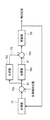
次に、S14の位置合わせ処理の詳細について説明する。図3は、本実施形態における位置合わせ処理の制御系を示すブロック線図である。図3のブロック線図における減算器16a、補償器16b、加算器16c、および生成器16dはそれぞれ、制御部16の構成要素として機能しうる。また、駆動部20は、例えば、モールド1と基板2とを相対的に駆動する駆動力(推力)を発生するアクチュエータと、該アクチュエータに電流(または電圧)を供給する供給器(電流ドライバ)とを含みうる。駆動部20は、上述したように、モールド駆動部11bおよび基板駆動部12bの少なくとも一方を含みうる。
[Alignment processing]
Next, the details of the alignment process in S14 will be described. FIG. 3 is a block diagram showing a control system for alignment processing in the present embodiment. The
モールド1と基板2との位置合わせ処理の制御系では、まず、計測部13によってモールド1と基板2との相対位置が計測され、その計測結果(相対位置を示す情報)が減算器16aに供給される。減算器16aは、計測部13により計測された相対位置と目標相対位置(例えばゼロ)との偏差30を算出して、算出した偏差30を出力する。補償器16bは、例えばPID補償器であり、減算器16aで算出された偏差30が低減するように(例えば、許容範囲に収まるように)駆動部20を制御するための第1信号31(第1指令値)を生成し、生成した第1信号31を駆動部20に供給する。駆動部20は、補償器16bで生成された第1信号31に従って、供給器によりアクチュエータに電流を供給し、アクチュエータに駆動力を発生させる。これにより、モールド1と基板2との相対位置が目標相対位置に近づくように、モールド1と基板2とを相対的に駆動することができる。
In the control system for the alignment process between the
このような位置合わせ処理は、上述したように、モールド1と基板上のインプリント材3とを接触させた状態において行われる。しかしながら、この状態では、インプリント材3の粘性により、モールド1と基板2との相対位置(XY方向)の変更を妨げるような抵抗力が働き、該相対位置を変更しづらくなる。その結果、位置合わせ処理に相応の時間を要し、スループットの点で不利になりうる。そこで、本実施形態のインプリント装置100は、位置合わせ処理において、駆動部20の駆動力を瞬間的に増加させる第2信号32(第2指令値)を時間間隔をあけながら第1信号31に加えて駆動部20に供給する。例えば、図3のブロック線図に示すように、第2信号32を生成する生成器16dが制御部16に設けられる。生成器16dは、時間間隔をあけながら第2信号32を離散的に生成して出力する。生成器16dから出力された第2信号32は、補償器16bから出力された第1信号31に加算器16cで加えられ(合成され)、合成信号として駆動部20に供給される。これにより、駆動部20の駆動力が瞬間的に且つ離散的に増加するため、あたかもハンマリングを行っているかのようにモールド1と基板2との相対位置を変更し、位置合わせ処理を効果的(効率的)に行うことができる。
As described above, such an alignment process is performed in a state where the
生成器16dは、例えば、駆動部20の駆動力を瞬間的に0.1N以上増加(より好ましくは0.5N以上増加)させる振幅を有するパルス信号(インパルス状の信号)を第2信号32として生成するとよい。第2信号32の振幅の最大値は、駆動部20で発生可能な最大駆動力によって制限されるが、好ましくは、駆動部20で瞬間的に発生する駆動力が1N以下となるように第2信号32を生成するとよい。また、生成器16dは、制御部16(CPU)の制御クロック周期以下、もしくは、フィードバック制御系のサンプリング周期以下のパルス幅を有するように、第2信号32を生成するとよい。より好ましくは、生成器16dは、制御部16(CPU)の制御クロック周期の1/2以下、もしくは、フィードバック制御系のサンプリング周期の1/2以下のパルス幅を有するように、第2信号32を生成するとよい。さらに、生成器16dは、第2信号32を離散的に出力する時間間隔を、第2信号32のパルス幅以上に設定するとよい。より好ましくは、生成器16dは、第2信号32を離散的に出力する時間間隔を、制御部16(CPU)の制御クロックの周期以上、もしくは、フィードバック制御系のサンプリング周期以上となるように設定するとよい。ここで、第2信号32のパルス幅は、振幅がその最大値の50%以上となる時間(いわゆる半値幅)として定義され、第2信号32は、三角形状または台形形状の信号を含みうる。
The
[第2信号の生成方法]
次に、生成器16dによる第2信号の生成方法について具体的に説明する。図4(a)は、減算器16aで算出された偏差30の時間変化を示す図であり、図4(b)は、生成器16dから出力される第2信号32を示す図である。以下では、減算器16aで算出された偏差30を単に「偏差30」と呼ぶことがあり、生成器16dが第2信号32を出力する時間間隔(駆動部20に第2信号32を供給する時間間隔)を単に「時間間隔」と呼ぶことがある。
[Method of generating the second signal]
Next, a method of generating the second signal by the
生成器16dは、図3のブロック線図に示すように、減算器16aで算出された偏差に基づいて、第2信号32の振幅、および第2信号32を出力する時間間隔を設定(決定)するように構成されうる。つまり、生成器16dは、減算器16aで算出された偏差30に基づいて、第2信号32の振幅および時間間隔の少なくとも一方を変更しうる。
As shown in the block diagram of FIG. 3, the
例えば、生成器16dは、第1閾値E1に対する偏差30の大小関係を判定し、その判定結果に応じて、第2信号32の振幅および時間間隔を変更する。図4に示すように、偏差30が第1閾値E1以上である場合には、生成器16dは、第2信号32の振幅を第1振幅A1に設定するとともに、時間間隔を第1間隔T1に設定する。そして、偏差30が第1閾値E1未満になった場合に、生成器16dは、第2信号32の振幅を、第1振幅A1より小さい第2振幅A2に設定するとともに、時間間隔を、第1間隔T1より広い第2間隔T2に設定する。第1振幅A1、第2振幅A2、第1間隔T1、および第2間隔T2は、第2信号の振幅および時間間隔をそれぞれ変化させたときのモールド1と基板2との相対位置の変化量について実験やシミュレーションを行い、その結果に基づいて事前に求められうる。また、偏差30が、第1閾値E1より小さい第2閾値E2未満になった場合には、生成器16dは、第2信号32の出力を停止する。即ち、偏差30が第2閾値E2未満になった場合に駆動部20(加算器16c)への第2信号32の供給が停止され、この後は、補償器16bにより生成された第1信号31のみが駆動部20(加算器16c)に供給される。
For example,
ここで、図4に示す例では、第1閾値E1に対する偏差の大小関係を判定した結果に応じて、第2信号32の振幅および時間間隔の双方を変更したが、それに限られるものではなく、第2信号32の振幅および時間間隔の少なくとも一方を変更してもよい。また、図4に示す例では、生成器16dは、第1閾値E1に対する偏差の大小関係に応じて第2信号32の振幅および時間間隔を変更したが、第1閾値E1を設定せずに、第2信号32の振幅および時間間隔の少なくとも一方を変更してもよい。例えば、生成器16dは、第1閾値E1を設定せず、減算器16aで算出された偏差30が小さくなるにつれて第2信号32の振幅を小さくしたり時間間隔を広げたりし、当該偏差30が第2閾値E2未満になった場合に第2信号32の出力を停止してもよい。この場合、生成器16dは、偏差30と第2信号32の振幅および時間間隔との関係を示す情報を用いるとよい。当該情報は、第2信号の振幅および時間間隔をそれぞれ変化させたときのモールド1と基板2との相対位置の変化量について実験やシミュレーションを行い、その結果に基づいて事前に求められうる。
Here, in the example shown in FIG. 4, both the amplitude and the time interval of the
上述したように、本実施形態のインプリント装置100は、位置合わせ処理において、駆動部の駆動力を瞬間的に増加させるための第2信号(第2指令値)を時間間隔をあけながら第1信号に加えて駆動部に供給する。これにより、駆動部の駆動力を瞬間的に且つ離散的に増加させて、モールド1と基板2との相対位置を効果的に変更することができる。
As described above, in the
<第2実施形態>
第1実施形態では、減算器16aで算出された偏差30に基づいて、第2信号32の振幅および時間間隔の少なくとも一方を変更する制御について説明した。第2実施形態では、位置合わせ処理中におけるモールド1と基板2との相対速度(XY方向)に基づいて、第2信号32の振幅および時間間隔の少なくとも一方を変更する制御について説明する。ここで、モールド1と基板2との相対速度とは、単位時間あたりにおける当該相対位置の変化量として定義することができ、以下では単に「相対速度」と呼ぶことがある。また、本実施形態は、第1実施形態のインプリント装置100の装置構成を引き継ぐものである。そして、本実施形態では、「相対速度に基づく第2信号32の供給制御」を、第1実施形態で説明した「減算器16aで算出された偏差30に基づく第2信号の供給制御」と併用して行ってもよい。
<Second Embodiment>
In the first embodiment, the control of changing at least one of the amplitude and the time interval of the
相対速度が目標速度(規定速度)に達していない場合、位置合わせ処理に相応の時間を要し、スループットの点で不利になりうる。そのため、本実施形態の生成器16d(制御部16)は、相対速度に応じて、第2信号32の振幅および時間間隔の少なくとも一方を変更しうる。例えば、生成器16dは、相対速度が目標速度より小さいか否か(大小関係)を判定し、相対速度が目標速度より小さいと判定した場合には、相対速度と目標速度との差に応じて、第2信号の振幅を大きくしたり時間間隔を狭めたりしうる。このとき、生成器16dは、相対速度と目標速度との差と、第2信号の振幅および時間間隔の変更量との関係を示す情報を用いるとよい。当該情報は、第2信号の振幅および時間間隔を変化させたときのモールド1と基板2との相対位置の変化量について実験やシミュレーションを行い、その結果に基づいて事前に求められうる。
If the relative speed does not reach the target speed (specified speed), the alignment process requires a considerable amount of time, which may be disadvantageous in terms of throughput. Therefore, the
ここで、生成器16d(制御部16)は、相対速度を、例えば、位置計測部17での計測結果に基づいて取得することができる。生成器16dは、相対速度を、減算器16aで算出された偏差30の変化量から推定してもよい。また、相対速度は、モールド1と基板上のインプリント材3との押圧力に応じて変わりうる。したがって、生成器16dは、モールド1とインプリント材3との押圧力を検出する検出部をインプリントヘッド11または基板ステージ12に設け、当該検出部での検出結果に基づいて、相対速度を推定してもよい。さらに、相対速度は、インプリント処理を行う対象ショット領域の基板上における位置に応じて変わりうる。例えば、基板のエッジ付近は、中心付近と比べて表面処理の状態や凹凸の状態が異なる場合があり、その場合、モールド1と基板2との相対位置を妨げる抵抗力も、基板のエッジ付近と中心付近とで異なりうる。したがって、生成器16dは、基板上における対象ショット領域の位置に基づいて、相対速度を推定してもよい。
Here, the
上述したように、本実施形態のインプリント装置は、相対速度に応じて、第2信号32の振幅および時間間隔の少なくとも一方を変更しうる。これにより、モールド1と基板2との相対位置を効果的に変更することができる。
As described above, the imprinting apparatus of this embodiment can change at least one of the amplitude and the time interval of the
<物品の製造方法の実施形態>
本発明の実施形態にかかる物品の製造方法は、例えば、半導体デバイス等のマイクロデバイスや微細構造を有する素子等の物品を製造するのに好適である。本実施形態の物品の製造方法は、基板に供給(塗布)されたインプリント材に上記のインプリント装置(インプリント方法)を用いてパターンを形成する工程と、かかる工程でパターンを形成された基板を加工する工程とを含む。更に、かかる製造方法は、他の周知の工程(酸化、成膜、蒸着、ドーピング、平坦化、エッチング、レジスト剥離、ダイシング、ボンディング、パッケージング等)を含む。本実施形態の物品の製造方法は、従来の方法に比べて、物品の性能・品質・生産性・生産コストの少なくとも1つにおいて有利である。
<Embodiment of manufacturing method of article>
The method for manufacturing an article according to the embodiment of the present invention is suitable for producing an article such as a microdevice such as a semiconductor device or an element having a fine structure, for example. The method for manufacturing an article of the present embodiment includes a step of forming a pattern on an imprint material supplied (coated) to a substrate by using the above-mentioned imprint device (imprint method), and a pattern is formed by such a step. Includes the process of processing the substrate. Further, such a manufacturing method includes other well-known steps (oxidation, film formation, vapor deposition, doping, flattening, etching, resist peeling, dicing, bonding, packaging, etc.). The method for producing an article of the present embodiment is advantageous in at least one of the performance, quality, productivity, and production cost of the article as compared with the conventional method.
インプリント装置を用いて成形した硬化物のパターンは、各種物品の少なくとも一部に恒久的に、或いは各種物品を製造する際に一時的に、用いられる。物品とは、電気回路素子、光学素子、MEMS、記録素子、センサ、或いは、型等である。電気回路素子としては、DRAM、SRAM、フラッシュメモリ、MRAMのような、揮発性或いは不揮発性の半導体メモリや、LSI、CCD、イメージセンサ、FPGAのような半導体素子等が挙げられる。型としては、インプリント用のモールド等が挙げられる。 The pattern of the cured product formed by using the imprint device is used permanently for at least a part of various articles or temporarily in manufacturing various articles. The article is an electric circuit element, an optical element, a MEMS, a recording element, a sensor, a mold, or the like. Examples of the electric circuit element include volatile or non-volatile semiconductor memories such as DRAM, SRAM, flash memory, and MRAM, and semiconductor elements such as LSI, CCD, image sensor, and FPGA. Examples of the mold include a mold for imprinting.
硬化物のパターンは、上記物品の少なくとも一部の構成部材として、そのまま用いられるか、或いは、レジストマスクとして一時的に用いられる。基板の加工工程においてエッチング又はイオン注入等が行われた後、レジストマスクは除去される。 The pattern of the cured product is used as it is as a constituent member of at least a part of the above-mentioned article, or is temporarily used as a resist mask. The resist mask is removed after etching, ion implantation, or the like in the substrate processing process.
次に、物品の具体的な製造方法について説明する。図5(a)に示すように、絶縁体等の被加工材2zが表面に形成されたシリコンウェハ等の基板1zを用意し、続いて、インクジェット法等により、被加工材2zの表面にインプリント材3zを付与する。ここでは、複数の液滴状になったインプリント材3zが基板上に付与された様子を示している。
Next, a specific manufacturing method of the article will be described. As shown in FIG. 5A, a
図5(b)に示すように、インプリント用の型4zを、その凹凸パターンが形成された側を基板上のインプリント材3zに向け、対向させる。図5(c)に示すように、インプリント材3zが付与された基板1zと型4zとを接触させ、圧力を加える。インプリント材3zは型4zと被加工材2zとの隙間に充填される。この状態で硬化用のエネルギーとして光を型4zを透して照射すると、インプリント材3zは硬化する。
As shown in FIG. 5B, the
図5(d)に示すように、インプリント材3zを硬化させた後、型4zと基板1zを引き離すと、基板1z上にインプリント材3zの硬化物のパターンが形成される。この硬化物のパターンは、型の凹部が硬化物の凸部に、型の凹部が硬化物の凸部に対応した形状になっており、即ち、インプリント材3zに型4zの凹凸パターンが転写されたことになる。
As shown in FIG. 5D, when the
図5(e)に示すように、硬化物のパターンを耐エッチングマスクとしてエッチングを行うと、被加工材2zの表面のうち、硬化物が無いか或いは薄く残存した部分が除去され、溝5zとなる。図5(f)に示すように、硬化物のパターンを除去すると、被加工材2zの表面に溝5zが形成された物品を得ることができる。ここでは硬化物のパターンを除去したが、加工後も除去せずに、例えば、半導体素子等に含まれる層間絶縁用の膜、つまり、物品の構成部材として利用してもよい。
As shown in FIG. 5E, when etching is performed using the pattern of the cured product as an etching resistant mask, the portion of the surface of the
以上、本発明の好ましい実施形態について説明したが、本発明はこれらの実施形態に限定されないことはいうまでもなく、その要旨の範囲内で種々の変形および変更が可能である。 Although the preferred embodiments of the present invention have been described above, it goes without saying that the present invention is not limited to these embodiments, and various modifications and modifications can be made within the scope of the gist thereof.
1:モールド、2:基板、3:インプリント材、11:インプリントヘッド、12:基板ステージ、13:計測部、14:硬化部、15:吐出部、16:制御部、100:インプリント装置 1: Mold 2: Substrate 3: Imprint material, 11: Imprint head, 12: Substrate stage, 13: Measurement unit, 14: Curing unit, 15: Discharge unit, 16: Control unit, 100: Imprint device
Claims (10)
前記モールドと前記基板とを相対的に駆動する駆動部と、
前記モールドと前記基板との相対位置を計測する計測部と、
前記モールドと前記基板との位置合わせにおいて、前記計測部で計測された前記相対位置と目標相対位置との偏差に応じた第1信号に、前記駆動部の駆動力を瞬間的に増加させる第2信号を時間間隔をあけながら合成した信号に基づいて前記駆動部を制御する制御部と、
を含むことを特徴とするインプリント装置。 An imprinting device that forms a pattern of imprinting material on a substrate using a mold.
A drive unit that relatively drives the mold and the substrate,
A measuring unit that measures the relative position between the mold and the substrate,
In the alignment between the mold and the substrate, the driving force of the driving unit is instantaneously increased to the first signal corresponding to the deviation between the relative position and the target relative position measured by the measuring unit. A control unit that controls the drive unit based on a signal obtained by synthesizing signals at time intervals.
An imprinting device characterized by including.
前記形成工程でパターンが形成された前記基板を加工する加工工程と、を含み、
前記加工工程で加工された前記基板から物品を製造することを特徴とする物品の製造方法。 A forming step of forming a pattern on a substrate by using the imprinting apparatus according to any one of claims 1 to 9.
Including a processing step of processing the substrate on which a pattern is formed in the forming step.
A method for producing an article, which comprises producing an article from the substrate processed in the processing step.
Priority Applications (3)
| Application Number | Priority Date | Filing Date | Title |
|---|---|---|---|
| JP2017131489A JP6882103B2 (en) | 2017-07-04 | 2017-07-04 | Imprinting equipment and manufacturing method of goods |
| US16/025,279 US11099491B2 (en) | 2017-07-04 | 2018-07-02 | Imprint apparatus, imprint method, and method of manufacturing article |
| KR1020180076354A KR102301911B1 (en) | 2017-07-04 | 2018-07-02 | Imprint apparatus, imprint method, and method of manufacturing article |
Applications Claiming Priority (1)
| Application Number | Priority Date | Filing Date | Title |
|---|---|---|---|
| JP2017131489A JP6882103B2 (en) | 2017-07-04 | 2017-07-04 | Imprinting equipment and manufacturing method of goods |
Publications (2)
| Publication Number | Publication Date |
|---|---|
| JP2019016656A JP2019016656A (en) | 2019-01-31 |
| JP6882103B2 true JP6882103B2 (en) | 2021-06-02 |
Family
ID=64903173
Family Applications (1)
| Application Number | Title | Priority Date | Filing Date |
|---|---|---|---|
| JP2017131489A Active JP6882103B2 (en) | 2017-07-04 | 2017-07-04 | Imprinting equipment and manufacturing method of goods |
Country Status (3)
| Country | Link |
|---|---|
| US (1) | US11099491B2 (en) |
| JP (1) | JP6882103B2 (en) |
| KR (1) | KR102301911B1 (en) |
Family Cites Families (19)
| Publication number | Priority date | Publication date | Assignee | Title |
|---|---|---|---|---|
| JPS62235788A (en) | 1986-04-07 | 1987-10-15 | Hitachi Ltd | Driving method for electrostrictive element |
| US7292326B2 (en) | 2004-11-30 | 2007-11-06 | Molecular Imprints, Inc. | Interferometric analysis for the manufacture of nano-scale devices |
| US7630067B2 (en) | 2004-11-30 | 2009-12-08 | Molecular Imprints, Inc. | Interferometric analysis method for the manufacture of nano-scale devices |
| US7446854B2 (en) * | 2006-02-07 | 2008-11-04 | Asml Netherlands B.V. | Lithographic apparatus and device manufacturing method |
| EP2584408B1 (en) * | 2007-02-06 | 2020-10-07 | Canon Kabushiki Kaisha | Imprint method and imprint apparatus |
| US8014881B2 (en) * | 2007-02-15 | 2011-09-06 | Asml Netherlands B.V. | Lithographic apparatus and device manufacturing method |
| US7710540B2 (en) * | 2007-04-05 | 2010-05-04 | Asml Netherlands B.V. | Lithographic apparatus and device manufacturing method |
| JP5279397B2 (en) * | 2008-08-06 | 2013-09-04 | キヤノン株式会社 | Imprint apparatus, imprint method, and device manufacturing method |
| JP2011124346A (en) * | 2009-12-09 | 2011-06-23 | Canon Inc | Imprint apparatus and article manufacturing method |
| JP5024464B2 (en) * | 2011-01-31 | 2012-09-12 | 株式会社日立製作所 | Pattern forming method and mold |
| JP2013021155A (en) * | 2011-07-12 | 2013-01-31 | Canon Inc | Imprint apparatus and method of manufacturing product using the same |
| JP5687640B2 (en) * | 2012-02-15 | 2015-03-18 | 株式会社東芝 | Imprint apparatus and imprint method |
| JP6039917B2 (en) * | 2012-05-22 | 2016-12-07 | キヤノン株式会社 | Imprint apparatus, imprint method, and article manufacturing method |
| JP6294686B2 (en) * | 2014-02-04 | 2018-03-14 | キヤノン株式会社 | Imprint apparatus, imprint method, and article manufacturing method |
| JP6497849B2 (en) | 2014-04-15 | 2019-04-10 | キヤノン株式会社 | Imprint apparatus and article manufacturing method |
| JP6465577B2 (en) | 2014-07-11 | 2019-02-06 | キヤノン株式会社 | Imprint apparatus and article manufacturing method |
| JP6562795B2 (en) * | 2015-02-12 | 2019-08-21 | キヤノン株式会社 | Imprint apparatus and article manufacturing method |
| JP6590598B2 (en) * | 2015-08-31 | 2019-10-16 | キヤノン株式会社 | Imprint apparatus, imprint method, and article manufacturing method |
| JP2017063111A (en) | 2015-09-24 | 2017-03-30 | キヤノン株式会社 | Mold, imprint method, imprint device, and article manufacturing method |
-
2017
- 2017-07-04 JP JP2017131489A patent/JP6882103B2/en active Active
-
2018
- 2018-07-02 KR KR1020180076354A patent/KR102301911B1/en active IP Right Grant
- 2018-07-02 US US16/025,279 patent/US11099491B2/en active Active
Also Published As
| Publication number | Publication date |
|---|---|
| KR102301911B1 (en) | 2021-09-15 |
| JP2019016656A (en) | 2019-01-31 |
| US11099491B2 (en) | 2021-08-24 |
| KR20190004658A (en) | 2019-01-14 |
| US20190011844A1 (en) | 2019-01-10 |
Similar Documents
| Publication | Publication Date | Title |
|---|---|---|
| US11175598B2 (en) | Imprint apparatus and method of manufacturing article | |
| JP7204464B2 (en) | IMPRINT METHOD, IMPRINT APPARATUS, AND ARTICLE MANUFACTURING METHOD | |
| JP7134055B2 (en) | Molding apparatus and article manufacturing method | |
| JP6875879B2 (en) | Imprinting equipment, imprinting methods, and manufacturing methods for goods | |
| JP7116552B2 (en) | IMPRINT APPARATUS AND ARTICLE MANUFACTURING METHOD | |
| JP6853704B2 (en) | Lithography equipment and manufacturing method of goods | |
| JP6882103B2 (en) | Imprinting equipment and manufacturing method of goods | |
| JP7403325B2 (en) | Imprint method, imprint device, and article manufacturing method | |
| JP7241623B2 (en) | Methods of Forming and Making Articles | |
| JP2022117092A (en) | Imprint method, imprint apparatus, and method of manufacturing article | |
| US11714352B2 (en) | Imprinting apparatus, imprinting method, method for producing article, substrate, and mold | |
| JP7257817B2 (en) | IMPRINT APPARATUS AND ARTICLE MANUFACTURING METHOD | |
| JP7451141B2 (en) | Imprint device, imprint method, and article manufacturing method | |
| JP7179655B2 (en) | IMPRINT APPARATUS, IMPRINT METHOD, AND ARTICLE MANUFACTURING METHOD | |
| JP7148284B2 (en) | IMPRINT APPARATUS AND ARTICLE MANUFACTURING METHOD | |
| JP2019067917A (en) | Imprint apparatus, imprint method, and article manufacturing method | |
| JP7362429B2 (en) | Molding equipment, molding method, and article manufacturing method | |
| JP7278163B2 (en) | IMPRINT APPARATUS AND ARTICLE MANUFACTURING METHOD | |
| JP7225030B2 (en) | IMPRINT METHOD AND ARTICLE MANUFACTURING METHOD | |
| JP6864447B2 (en) | Lithography equipment and manufacturing method of goods | |
| KR102330969B1 (en) | Imprint apparatus, and method of manufacturing article | |
| JP2018018944A (en) | Imprint method and manufacturing method of article | |
| KR102211390B1 (en) | Imprint device and article manufacturing method | |
| JP6818523B2 (en) | Manufacturing method of imprinting equipment and articles | |
| JP2023083029A (en) | Imprint method, pattern formation method, imprint device, mold for imprinting, and manufacturing method for article |
Legal Events
| Date | Code | Title | Description |
|---|---|---|---|
| A621 | Written request for application examination |
Free format text: JAPANESE INTERMEDIATE CODE: A621 Effective date: 20200529 |
|
| RD01 | Notification of change of attorney |
Free format text: JAPANESE INTERMEDIATE CODE: A7421 Effective date: 20210103 |
|
| A521 | Written amendment |
Free format text: JAPANESE INTERMEDIATE CODE: A523 Effective date: 20210113 |
|
| TRDD | Decision of grant or rejection written | ||
| A01 | Written decision to grant a patent or to grant a registration (utility model) |
Free format text: JAPANESE INTERMEDIATE CODE: A01 Effective date: 20210402 |
|
| A61 | First payment of annual fees (during grant procedure) |
Free format text: JAPANESE INTERMEDIATE CODE: A61 Effective date: 20210506 |
|
| R151 | Written notification of patent or utility model registration |
Ref document number: 6882103 Country of ref document: JP Free format text: JAPANESE INTERMEDIATE CODE: R151 |