JP6880190B2 - All solid state optical transmission / receiver terminal - Google Patents
All solid state optical transmission / receiver terminal Download PDFInfo
- Publication number
- JP6880190B2 JP6880190B2 JP2019529186A JP2019529186A JP6880190B2 JP 6880190 B2 JP6880190 B2 JP 6880190B2 JP 2019529186 A JP2019529186 A JP 2019529186A JP 2019529186 A JP2019529186 A JP 2019529186A JP 6880190 B2 JP6880190 B2 JP 6880190B2
- Authority
- JP
- Japan
- Prior art keywords
- optical
- lens
- reception terminal
- optical switch
- planar
- Prior art date
- Legal status (The legal status is an assumption and is not a legal conclusion. Google has not performed a legal analysis and makes no representation as to the accuracy of the status listed.)
- Active
Links
Images


Classifications
-
- G—PHYSICS
- G02—OPTICS
- G02B—OPTICAL ELEMENTS, SYSTEMS OR APPARATUS
- G02B6/00—Light guides; Structural details of arrangements comprising light guides and other optical elements, e.g. couplings
- G02B6/24—Coupling light guides
- G02B6/26—Optical coupling means
- G02B6/35—Optical coupling means having switching means
- G02B6/354—Switching arrangements, i.e. number of input/output ports and interconnection types
- G02B6/3544—2D constellations, i.e. with switching elements and switched beams located in a plane
- G02B6/3548—1xN switch, i.e. one input and a selectable single output of N possible outputs
-
- B—PERFORMING OPERATIONS; TRANSPORTING
- B81—MICROSTRUCTURAL TECHNOLOGY
- B81B—MICROSTRUCTURAL DEVICES OR SYSTEMS, e.g. MICROMECHANICAL DEVICES
- B81B3/00—Devices comprising flexible or deformable elements, e.g. comprising elastic tongues or membranes
- B81B3/0064—Constitution or structural means for improving or controlling the physical properties of a device
- B81B3/0083—Optical properties
-
- G—PHYSICS
- G01—MEASURING; TESTING
- G01S—RADIO DIRECTION-FINDING; RADIO NAVIGATION; DETERMINING DISTANCE OR VELOCITY BY USE OF RADIO WAVES; LOCATING OR PRESENCE-DETECTING BY USE OF THE REFLECTION OR RERADIATION OF RADIO WAVES; ANALOGOUS ARRANGEMENTS USING OTHER WAVES
- G01S17/00—Systems using the reflection or reradiation of electromagnetic waves other than radio waves, e.g. lidar systems
- G01S17/88—Lidar systems specially adapted for specific applications
- G01S17/89—Lidar systems specially adapted for specific applications for mapping or imaging
-
- G—PHYSICS
- G01—MEASURING; TESTING
- G01S—RADIO DIRECTION-FINDING; RADIO NAVIGATION; DETERMINING DISTANCE OR VELOCITY BY USE OF RADIO WAVES; LOCATING OR PRESENCE-DETECTING BY USE OF THE REFLECTION OR RERADIATION OF RADIO WAVES; ANALOGOUS ARRANGEMENTS USING OTHER WAVES
- G01S7/00—Details of systems according to groups G01S13/00, G01S15/00, G01S17/00
- G01S7/48—Details of systems according to groups G01S13/00, G01S15/00, G01S17/00 of systems according to group G01S17/00
- G01S7/481—Constructional features, e.g. arrangements of optical elements
- G01S7/4814—Constructional features, e.g. arrangements of optical elements of transmitters alone
-
- G—PHYSICS
- G01—MEASURING; TESTING
- G01S—RADIO DIRECTION-FINDING; RADIO NAVIGATION; DETERMINING DISTANCE OR VELOCITY BY USE OF RADIO WAVES; LOCATING OR PRESENCE-DETECTING BY USE OF THE REFLECTION OR RERADIATION OF RADIO WAVES; ANALOGOUS ARRANGEMENTS USING OTHER WAVES
- G01S7/00—Details of systems according to groups G01S13/00, G01S15/00, G01S17/00
- G01S7/48—Details of systems according to groups G01S13/00, G01S15/00, G01S17/00 of systems according to group G01S17/00
- G01S7/481—Constructional features, e.g. arrangements of optical elements
- G01S7/4816—Constructional features, e.g. arrangements of optical elements of receivers alone
-
- G—PHYSICS
- G01—MEASURING; TESTING
- G01S—RADIO DIRECTION-FINDING; RADIO NAVIGATION; DETERMINING DISTANCE OR VELOCITY BY USE OF RADIO WAVES; LOCATING OR PRESENCE-DETECTING BY USE OF THE REFLECTION OR RERADIATION OF RADIO WAVES; ANALOGOUS ARRANGEMENTS USING OTHER WAVES
- G01S7/00—Details of systems according to groups G01S13/00, G01S15/00, G01S17/00
- G01S7/48—Details of systems according to groups G01S13/00, G01S15/00, G01S17/00 of systems according to group G01S17/00
- G01S7/481—Constructional features, e.g. arrangements of optical elements
- G01S7/4817—Constructional features, e.g. arrangements of optical elements relating to scanning
-
- G—PHYSICS
- G02—OPTICS
- G02B—OPTICAL ELEMENTS, SYSTEMS OR APPARATUS
- G02B26/00—Optical devices or arrangements for the control of light using movable or deformable optical elements
- G02B26/007—Optical devices or arrangements for the control of light using movable or deformable optical elements the movable or deformable optical element controlling the colour, i.e. a spectral characteristic, of the light
-
- G—PHYSICS
- G02—OPTICS
- G02B—OPTICAL ELEMENTS, SYSTEMS OR APPARATUS
- G02B6/00—Light guides; Structural details of arrangements comprising light guides and other optical elements, e.g. couplings
- G02B6/24—Coupling light guides
- G02B6/26—Optical coupling means
- G02B6/35—Optical coupling means having switching means
- G02B6/351—Optical coupling means having switching means involving stationary waveguides with moving interposed optical elements
- G02B6/3524—Optical coupling means having switching means involving stationary waveguides with moving interposed optical elements the optical element being refractive
- G02B6/3526—Optical coupling means having switching means involving stationary waveguides with moving interposed optical elements the optical element being refractive the optical element being a lens
-
- G—PHYSICS
- G02—OPTICS
- G02B—OPTICAL ELEMENTS, SYSTEMS OR APPARATUS
- G02B6/00—Light guides; Structural details of arrangements comprising light guides and other optical elements, e.g. couplings
- G02B6/24—Coupling light guides
- G02B6/26—Optical coupling means
- G02B6/35—Optical coupling means having switching means
- G02B6/351—Optical coupling means having switching means involving stationary waveguides with moving interposed optical elements
- G02B6/3534—Optical coupling means having switching means involving stationary waveguides with moving interposed optical elements the optical element being diffractive, i.e. a grating
-
- G—PHYSICS
- G02—OPTICS
- G02B—OPTICAL ELEMENTS, SYSTEMS OR APPARATUS
- G02B6/00—Light guides; Structural details of arrangements comprising light guides and other optical elements, e.g. couplings
- G02B6/24—Coupling light guides
- G02B6/26—Optical coupling means
- G02B6/35—Optical coupling means having switching means
- G02B6/354—Switching arrangements, i.e. number of input/output ports and interconnection types
- G02B6/3544—2D constellations, i.e. with switching elements and switched beams located in a plane
- G02B6/3548—1xN switch, i.e. one input and a selectable single output of N possible outputs
- G02B6/355—1x2 switch, i.e. one input and a selectable single output of two possible outputs
-
- H—ELECTRICITY
- H04—ELECTRIC COMMUNICATION TECHNIQUE
- H04J—MULTIPLEX COMMUNICATION
- H04J14/00—Optical multiplex systems
- H04J14/02—Wavelength-division multiplex systems
- H04J14/0201—Add-and-drop multiplexing
- H04J14/0215—Architecture aspects
- H04J14/022—For interconnection of WDM optical networks
-
- H—ELECTRICITY
- H04—ELECTRIC COMMUNICATION TECHNIQUE
- H04Q—SELECTING
- H04Q11/00—Selecting arrangements for multiplex systems
- H04Q11/0001—Selecting arrangements for multiplex systems using optical switching
- H04Q11/0003—Details
-
- H—ELECTRICITY
- H04—ELECTRIC COMMUNICATION TECHNIQUE
- H04Q—SELECTING
- H04Q11/00—Selecting arrangements for multiplex systems
- H04Q11/0001—Selecting arrangements for multiplex systems using optical switching
- H04Q11/0005—Switch and router aspects
-
- B—PERFORMING OPERATIONS; TRANSPORTING
- B81—MICROSTRUCTURAL TECHNOLOGY
- B81B—MICROSTRUCTURAL DEVICES OR SYSTEMS, e.g. MICROMECHANICAL DEVICES
- B81B2201/00—Specific applications of microelectromechanical systems
- B81B2201/04—Optical MEMS
- B81B2201/045—Optical switches
-
- G—PHYSICS
- G02—OPTICS
- G02B—OPTICAL ELEMENTS, SYSTEMS OR APPARATUS
- G02B6/00—Light guides; Structural details of arrangements comprising light guides and other optical elements, e.g. couplings
- G02B6/10—Light guides; Structural details of arrangements comprising light guides and other optical elements, e.g. couplings of the optical waveguide type
- G02B6/12—Light guides; Structural details of arrangements comprising light guides and other optical elements, e.g. couplings of the optical waveguide type of the integrated circuit kind
- G02B2006/12133—Functions
- G02B2006/12145—Switch
Description
(関連出願の相互参照)
本願は、米国仮特許出願第62/498,158号、出願日2016年12月16日、発明の名称”All−solid state optical transmit/receive terminal”、米国仮特許出願第62/450,855号、出願日2017年1月26日、発明の名称”Method and Apparatus for Light Field Generation”、および米国仮特許出願第62/516,602号、出願日2017年6月7日、発明の名称”Integrated MEMS Switches for Selectively Coupling Light In and Out of a Waveguide”の利益を主張するものであり、これらの各々の全内容は、あらゆる目的のために参照により本明細書中に援用される。
(Cross-reference of related applications)
This application is based on US provisional patent application No. 62 / 498,158, filing date December 16, 2016, title of invention "All-solid state optional transition / receive tertiary", US provisional patent application No. 62 / 450,855. , Filing date January 26, 2017, title of invention "Method and Apparatus for Light Field Generation", and US Provisional Patent Application No. 62 / 516,602, filing date June 7, 2017, title of invention "Integrated" It claims the interests of "MEMS Switch for Selective Patenting Light In and Out of a Waveguide", the entire contents of which are incorporated herein by reference for all purposes.
本発明は、光学スイッチネットワークに関し、より具体的には、光方向および測距(LiDAR)およびレーザ通信システム等において、光学信号が伝送または受信される方向を制御するために使用される光学スイッチネットワークに関する。 The present invention relates to an optical switch network, more specifically, an optical switch network used to control a direction in which an optical signal is transmitted or received in an optical direction and distance measurement (LiDAR), a laser communication system, or the like. Regarding.
多くの光学システムは、高精度を伴って制御され得る方向における(人間に視認可能または視認不可能な)コリメート光学ビームを放出または受光する必要がある。例えば、そのような光学ビームは、光方向および測距(LiDAR)システムにおいて使用され、多くの場合、これらのビームは、標的を位置特定または追跡するために操向または掃引される必要がある。同様に、レーザ通信システムは、時として、2つの端末の間で最初に見通し内通信チャネルを確立するため、または端末の一方または両方が移動する場合等に、光学ビームを操向する必要がある。 Many optical systems need to emit or receive a collimated optical beam (visible or invisible to humans) in a direction that can be controlled with high precision. For example, such optical beams are used in light direction and range (LiDAR) systems, and often these beams need to be steered or swept to locate or track a target. Similarly, laser communication systems sometimes need to steer an optical beam to first establish an in-line line communication channel between two terminals, or when one or both of the terminals move. ..
先行技術のLiDARおよびレーザ通信端末は、米国特許公開第2007/0229994号によって例示されるように、望遠鏡を使用し、ジンバルを使用して、望遠鏡全体を向けるか、または移動可能な操向鏡を望遠鏡の正面に設置し、鏡を使用するかのいずれか一方を行い、ビームを再指向する。しかしながら、本アプローチは、サイズ、質量、電力、および信頼性の観点から付随する欠点を伴う、大型の嵩張る移動システムを要求する。 Prior art LiDAR and laser communication terminals use a telescope and a gimbal to point the entire telescope or move a steering mirror, as illustrated by US Patent Publication No. 2007/0229994. Place it in front of the telescope and either use the mirror to redirect the beam. However, this approach requires a large, bulky mobile system with associated drawbacks in terms of size, mass, power, and reliability.
ビーム操向の他の従来の方法は、多数のアンテナがともに近接してアレイ化され、コヒーレントに動作される、すなわち、個々のエミッタの位相が慎重に制御され、アレイ全体を調和して動作させる、光学位相アレイを伴う。近接場における信号は、建設的および破壊的に干渉し、所望される方向にヌルおよび強化信号を作成する。しかしながら、位相アレイは、多数のエミッタおよび関連付けられる光学位相調節器を要求する。 Other conventional methods of beam steering have multiple antennas arrayed together in close proximity and operated coherently, i.e., the phase of the individual emitters is carefully controlled to operate the entire array in harmony. , With an optical phase array. Signals in close field interfere constructively and destructively, creating null and enhanced signals in the desired direction. However, phase arrays require a large number of emitters and associated optical phase adjusters.
公称光学位相アレイは、半波長間隔で、すなわち、約0.5μmで配置される、エミッタを有する。長距離レーザ通信等の用途のために、要求される総開口サイズは、約5cmである場合がある。したがって、104×104個のエミッタおよび位相偏移器のアレイが、必要とされるであろう。現在実証されているように、位相偏移器は、動作するために約1メガワットの電力を要求する。したがって、そのようなアレイの総電力消費量は、105ワット、すなわち、非現実的に多量の電力に迫り得る。しかしながら、バイナリ光学スイッチが加工され得る密度の限界が、伝送/受信端末の空間分解能、すなわち、可能性として考えられる伝送または受信ビーム位置の密度を限定する。 Nominal optical phase arrays have emitters arranged at half wavelength intervals, i.e. about 0.5 μm. For applications such as long-range laser communication, the total aperture size required may be about 5 cm. Thus, 10 4 × 10 4 cells of the array of emitters and phase shifter is, would be needed. As currently demonstrated, phase shifters require approximately 1 megawatt of power to operate. Therefore, the total power consumption of such an array, 105 watts, i.e., may be impractical approaching a large amount of power. However, the density limit at which the binary optical switch can be machined limits the spatial resolution of the transmission / reception terminal, i.e., the possible transmission or reception beam position density.
本発明のある実施形態は、光学送信/受信端末を提供する。光学送信/受信端末は、レンズと、光学スイッチネットワークとを含む。レンズは、視野を有する。光学スイッチネットワークは、平面状のN×1光学スイッチネットワークである。光学スイッチネットワークは、共通入力/出力ポートと、N個の他のポートとを有する。N個の他のポートは、N個の他のポートの各ポートがレンズ視野の一意の部分に光学的に結合されるように、レンズに光学的に結合される。光学送信/受信端末はまた、光学スイッチネットワークの共通入力/出力ポートに光学的に結合される、光学伝送機および/または光学受信機を含む。 One embodiment of the present invention provides an optical transmission / reception terminal. Optical transmission / reception terminals include a lens and an optical switch network. The lens has a field of view. The optical switch network is a planar N × 1 optical switch network. The optical switch network has a common input / output port and N other ports. The N other ports are optically coupled to the lens so that each port of the N other ports is optically coupled to a unique portion of the lens field of view. Optical transmit / receive terminals also include an optical transmitter and / or an optical receiver that is optically coupled to a common input / output port in an optical switch network.
N個の他のポートは、長方形アレイ内に配列されてもよい。 The N other ports may be arranged in a rectangular array.
N個の他のポートは、平面状の表面上に配置されてもよい。 The N other ports may be arranged on a flat surface.
光学スイッチネットワークは、光チップを含む、またはその上で加工されてもよい。 The optical switch network may include or be machined on an optical chip.
N個の他のポートの各ポートは、光学結合器を含んでもよい Each port of the N other ports may include an optical coupler.
光学送信/受信端末はまた、複数の光ファイバを含んでもよい。N個の他のポートの各ポートは、それぞれ、複数の光ファイバの少なくとも1つの光ファイバを介してレンズに光学的に結合されてもよい。 The optical transmission / reception terminal may also include a plurality of optical fibers. Each port of the N other ports may be optically coupled to the lens via at least one optical fiber of a plurality of optical fibers, respectively.
光学スイッチネットワークは、複数の光導波管を含んでもよい。複数の光導波管は、複数の光学接合部において交差してもよい。複数の光導波管および複数の光学接合部は、分岐した光導波管ネットワーク内に配列されてもよい。分岐した光導波管ネットワークは、ルートと、複数のリーフとを有してもよい。ルートは、共通入力/出力ポートに結合されてもよい。複数のリーフの各リーフは、N個の他のポートの個別のポートに結合されてもよい。光学スイッチネットワークはまた、複数のバイナリ光学スイッチを含んでもよい。複数のバイナリ光学スイッチの個別の1つのバイナリ光学スイッチは、複数の光学接合部の各光学接合部に配置されてもよい。 The optical switch network may include a plurality of optical waveguides. The plurality of optical waveguides may intersect at a plurality of optical junctions. The plurality of optical waveguides and the plurality of optical junctions may be arranged in a branched optical waveguide network. The branched optical waveguide network may have a root and a plurality of leaves. Routes may be coupled to common input / output ports. Each leaf of the plurality of leaves may be combined with a separate port of N other ports. The optical switch network may also include multiple binary optical switches. A separate binary optical switch for the plurality of binary optical switches may be located at each optical junction of the plurality of optical junctions.
分岐した光導波管ネットワークは、Hツリーを含んでもよい。 The branched optical waveguide network may include an H-tree.
光学スイッチネットワークは、光チップを含む、またはその上で加工されてもよい。 The optical switch network may include or be machined on an optical chip.
光学送信/受信端末はまた、行および列アドレス指定行列を含んでもよい。行および列アドレス指定行列は、複数の行と、複数の列とを有してもよい。複数のバイナリ光学スイッチの各バイナリ光学スイッチは、複数の行のうちの行に結合されてもよい。複数のバイナリ光学スイッチの各バイナリ光学スイッチは、複数の列のうちの列に結合されてもよい。複数のバイナリ光学スイッチの各バイナリ光学スイッチは、複数の行のうちの行および複数の列のうちの列の両方の上に存在する信号に応答して作動するように構成されてもよい。 Optical transmit / receive terminals may also include row and column addressing matrices. The row and column addressing matrix may have a plurality of rows and a plurality of columns. Each binary optical switch of a plurality of binary optical switches may be combined into a row of a plurality of rows. Each binary optical switch of the plurality of binary optical switches may be coupled to one of a plurality of columns. Each binary optical switch of the plurality of binary optical switches may be configured to operate in response to a signal existing on both the row of the rows and the column of the columns.
光学スイッチネットワークは、x−y平面内に存在してもよい。光学送信/受信端末は、x−y段を含んでもよい。x−y段は、レンズに機械的に結合されてもよい。x−y段は、レンズを、光学スイッチネットワークに対して、x−y平面に平行な平面内に偏移させるように構成されてもよい。 The optical switch network may reside in the xy plane. The optical transmission / reception terminal may include an xy stage. The xy stage may be mechanically coupled to the lens. The xy stage may be configured to shift the lens into a plane parallel to the xy plane with respect to the optical switch network.
レンズは、x−y平面内に存在してもよい。光学送信/受信端末は、x−y段を含んでもよい。x−y段は、光学スイッチネットワークに機械的に結合されてもよい。x−y段は、光学スイッチネットワークを、レンズに対して、x−y平面に平行な平面内に偏移させるように構成されてもよい。 The lens may be in the xy plane. The optical transmission / reception terminal may include an xy stage. The xy stage may be mechanically coupled to the optical switch network. The xy stage may be configured to shift the optical switch network into a plane parallel to the xy plane with respect to the lens.
光学送信/受信端末は、x−y段を含んでもよい。x−y段は、レンズおよび光学スイッチネットワークに機械的に結合されてもよい。x−y段は、レンズを、光学スイッチネットワーク光学系とともに平面内に偏移させるように構成されてもよい。 The optical transmission / reception terminal may include an xy stage. The xy stage may be mechanically coupled to the lens and optical switch network. The xy stage may be configured to shift the lens into a plane along with the optical switch network optics.
光学スイッチネットワークは、x−y平面内に存在してもよい。光学送信/受信端末は、レンズと光学スイッチネットワークとの間に光学的に配置される、中間光学系を含んでもよい。光学送信/受信端末はまた、x−y段を含んでもよい。x−y段は、中間光学系に機械的に結合されてもよい。x−y段は、中間光学系をx−y平面に平行な平面内に偏移させるように構成されてもよい。 The optical switch network may reside in the xy plane. The optical transmit / receive terminal may include an intermediate optical system that is optically located between the lens and the optical switch network. The optical transmission / reception terminal may also include an xy stage. The xy stage may be mechanically coupled to the intermediate optical system. The xy stage may be configured to shift the intermediate optical system into a plane parallel to the xy plane.
中間光学系は、小型レンズアレイを含んでもよい。 The intermediate optics may include a small lens array.
光学スイッチネットワークは、x−y平面内に存在してもよい。レンズは、少なくとも、第1の小型レンズアレイと、第1の小型レンズアレイに平行な第2の小型レンズアレイとを含んでもよい。光学送信/受信端末は、レンズと光学スイッチネットワークとの間に光学的に配置される、第3の小型レンズアレイを含んでもよい。光学送信/受信端末は、x−y段を含んでもよい。x−y段は、レンズに機械的に結合されてもよい。x−y段は、レンズをx−y平面に平行な平面内に偏移させるように構成されてもよい。
本明細書は、例えば、以下の項目も提供する。
(項目1)
光学送信/受信端末であって、
視野を有するレンズと、
共通入力/出力ポートと、N個の他のポートとを有する、平面状のN×1光学スイッチネットワークであって、前記N個の他のポートは、前記N個の他のポートの各ポートが前記レンズの視野の一意の部分に光学的に結合されるように、前記レンズに光学的に結合される、平面状のN×1光学スイッチネットワークと、
前記光学スイッチネットワークの共通入力/出力ポートに光学的に結合される光学伝送機および/または光受信機と
を備える、光学送信/受信端末。
(項目2)
前記N個の他のポートは、長方形アレイ内に配列される、項目1に記載の光学送信/受信端末。
(項目3)
前記N個の他のポートは、平面状の表面上に配置される、項目1−2のいずれかに記載の光学送信/受信端末。
(項目4)
前記光学スイッチネットワークは、光チップを備える、項目1−3のいずれかに記載の光学送信/受信端末。
(項目5)
前記N個の他のポートの各ポートは、光学結合器を備える、項目1−4のいずれかに記載の光学送信/受信端末。
(項目6)
複数の光ファイバをさらに備え、前記N個の他のポートの各ポートは、それぞれ、前記複数の光ファイバの少なくとも1つの光ファイバを介して前記レンズに光学的に結合される、項目1−5のいずれかに記載の光学送信/受信端末。
(項目7)
前記光学スイッチネットワークは、
複数の光学接合部において交差する複数の光学導波管であって、前記複数の光学導波管および前記複数の光学接合部は、ルートと、複数のリーフとを有する、分岐した光学導波管ネットワーク内に配列され、前記ルートは、前記共通入力/出力ポートに結合され、前記複数のリーフの各リーフは、前記N個の他のポートの個別のポートに結合される、複数の光学導波管と、
複数のバイナリ光学スイッチであって、前記複数のバイナリ光学スイッチの個別の1つのバイナリ光学スイッチは、前記複数の光学接合部の各光学接合部に配置される、複数のバイナリ光学スイッチと、
を備える、前述の項目のいずれかに記載の光学送信/受信端末。
(項目8)
前記分岐した光学導波管ネットワークは、Hツリーを備える、項目7に記載の光学送信/受信端末。
(項目9)
前記光学スイッチネットワークは、光チップを備える、項目7に記載の光学送信/受信端末。
(項目10)
複数の行と、複数の列とを有する、行および列アドレス指定行列をさらに備え、
前記複数のバイナリ光学スイッチの各バイナリ光学スイッチは、
前記複数の行のうちの行に結合され、
前記複数の列のうちの列に結合され、
前記複数の行のうちの前記行および前記複数の列のうちの前記列の両方の上に存在する信号に応答して作動するように構成される、
項目7に記載の光学送信/受信端末。
(項目11)
前記光学スイッチネットワークは、x−y平面内に存在し、前記光学送信/受信端末はさらに、
前記レンズに機械的に結合され、前記レンズを、前記光学スイッチネットワークに対して、前記x−y平面に平行な平面内に偏移させるように構成される、x−y段
を備える、項目1−10のいずれかに記載の光学送信/受信端末。
(項目12)
前記レンズは、x−y平面内に存在し、前記光学送信/受信端末はさらに、
前記光学スイッチネットワークに機械的に結合され、前記光学スイッチネットワークを、前記レンズに対して、前記x−y平面に平行な平面内に偏移させるように構成される、x−y段
を備える、項目1−11のいずれかに記載の光学送信/受信端末。
(項目13)
前記レンズおよび前記光学スイッチネットワークに機械的に結合され、前記レンズを、前記光学スイッチネットワーク光学系とともに平面内に偏移させるように構成される、x−y段をさらに備える、項目1−12のいずれかに記載の光学送信/受信端末。
(項目14)
前記光学スイッチネットワークは、x−y平面内に存在し、前記光学送信/受信端末はさらに、
前記レンズと前記光学スイッチネットワークとの間に光学的に配置される中間光学系と、
前記中間光学系に機械的に結合され、前記中間光学系を前記x−y平面に平行な平面内に偏移させるように構成される、x−y段と
を備える、項目1−13のいずれかに記載の光学送信/受信端末。
(項目15)
前記中間光学系は、小型レンズアレイを備える、項目14に記載の光学送信/受信端末。
(項目16)
前記光学スイッチネットワークは、x−y平面内に存在し、
前記レンズは、少なくとも、第1の小型レンズアレイと、前記第1の小型レンズアレイに平行な第2の小型レンズアレイとを備え、前記光学送信/受信端末はさらに、
前記レンズと前記光学スイッチネットワークとの間に光学的に配置される第3の小型レンズアレイと、
前記レンズに機械的に結合され、前記レンズを前記x−y平面に平行な平面内に偏移させるように構成される、x−y段と
を備える、項目1−15のいずれかに記載の光学送信/受信端末。
The optical switch network may reside in the xy plane. The lens may include at least a first small lens array and a second small lens array parallel to the first small lens array. The optical transmit / receive terminal may include a third small lens array that is optically located between the lens and the optical switch network. The optical transmission / reception terminal may include an xy stage. The xy stage may be mechanically coupled to the lens. The xy stage may be configured to shift the lens into a plane parallel to the xy plane.
The present specification also provides, for example, the following items.
(Item 1)
Optical transmission / reception terminal
With a lens that has a field of view
A planar N × 1 optical switch network having a common input / output port and N other ports, wherein the N other ports are each of the N other ports. A planar Nx1 optical switch network that is optically coupled to the lens so that it is optically coupled to a unique portion of the field of view of the lens.
With an optical transmitter and / or optical receiver optically coupled to a common input / output port of the optical switch network
Optical transmission / reception terminal.
(Item 2)
The optical transmission / reception terminal according to item 1, wherein the N other ports are arranged in a rectangular array.
(Item 3)
The optical transmission / reception terminal according to any one of items 1-2, wherein the N other ports are arranged on a flat surface.
(Item 4)
The optical transmission / reception terminal according to any one of items 1-3, wherein the optical switch network includes an optical chip.
(Item 5)
The optical transmission / reception terminal according to any one of items 1-4, wherein each port of the N other ports includes an optical coupler.
(Item 6)
Item 1-5, further comprising a plurality of optical fibers, each port of the N other ports being optically coupled to the lens via at least one optical fiber of the plurality of optical fibers. The optical transmission / reception terminal according to any one of.
(Item 7)
The optical switch network
A plurality of optical waveguides intersecting at a plurality of optical junctions, wherein the plurality of optical waveguides and the plurality of optical junctions are branched optical waveguides having a root and a plurality of leaves. Arranged within the network, the routes are coupled to the common input / output ports, and each leaf of the plurality of leaves is coupled to a separate port of the N other ports, a plurality of optical waveguides. Tube and
A plurality of binary optical switches, one of which is an individual binary optical switch of the plurality of binary optical switches, is a plurality of binary optical switches arranged at each optical junction of the plurality of optical junctions.
The optical transmission / reception terminal according to any one of the above items.
(Item 8)
The optical transmission / reception terminal according to item 7, wherein the branched optical waveguide network includes an H tree.
(Item 9)
The optical transmission / reception terminal according to item 7, wherein the optical switch network includes an optical chip.
(Item 10)
Further including a row and column addressing matrix with multiple rows and multiple columns,
Each binary optical switch of the plurality of binary optical switches
Combined with one of the multiple rows
Combined into one of the multiple columns
It is configured to operate in response to signals present on both the row of the rows and the column of the columns.
The optical transmission / reception terminal according to item 7.
(Item 11)
The optical switch network resides in the xy plane, and the optical transmit / receive terminal further comprises.
An xy stage that is mechanically coupled to the lens and is configured to shift the lens into a plane parallel to the xy plane with respect to the optical switch network.
The optical transmission / reception terminal according to any one of items 1-10.
(Item 12)
The lens resides in the xy plane and the optical transmit / receive terminal further
An xy stage that is mechanically coupled to the optical switch network and is configured to shift the optical switch network into a plane parallel to the xy plane with respect to the lens.
The optical transmission / reception terminal according to any one of items 1-11.
(Item 13)
Item 1-12, further comprising an xy stage, which is mechanically coupled to the lens and the optical switch network and configured to shift the lens into a plane with the optical switch network optics. The optical transmission / reception terminal according to any one.
(Item 14)
The optical switch network resides in the xy plane, and the optical transmit / receive terminal further comprises.
An intermediate optical system optically arranged between the lens and the optical switch network,
With an xy stage that is mechanically coupled to the intermediate optical system and configured to shift the intermediate optical system into a plane parallel to the xy plane.
The optical transmission / reception terminal according to any one of items 1-13.
(Item 15)
The optical transmission / reception terminal according to item 14, wherein the intermediate optical system includes a small lens array.
(Item 16)
The optical switch network exists in the xy plane and
The lens comprises at least a first small lens array and a second small lens array parallel to the first small lens array, and the optical transmission / reception terminal further comprises.
A third small lens array optically located between the lens and the optical switch network,
With an xy stage that is mechanically coupled to the lens and configured to shift the lens into a plane parallel to the xy plane.
The optical transmission / reception terminal according to any one of items 1-15.
本発明は、図面と併せて以下の特定の実施形態の詳細な説明を参照することによって、さらに完全に理解されるであろう。 The present invention will be further fully understood by reference to the detailed description of the particular embodiments below in conjunction with the drawings.
本発明の実施形態によると、全ソリッドステート光学伝送/受信端末のための方法および装置が、開示される。そのような端末は、光学ビームを操向するための機械的構成要素またはその付随する多数の位相偏移器を伴うエミッタ/コレクタの位相アレイを要求しない。代わりに、本端末は、光学ビームを操向するための光学スイッチを採用する。しかしながら、光学スイッチの比較的に小さいサブセットのみが、任意の所与の時間において動作され、したがって、給電される必要がある。したがって、本端末は、先行技術と関連付けられる、機械的なエミッタ密度および高電力問題を克服する。 According to embodiments of the present invention, methods and devices for all solid state optical transmission / reception terminals are disclosed. Such terminals do not require an emitter / collector phase array with a mechanical component or its associated multiple phase shifters to steer the optical beam. Instead, the terminal employs an optical switch to steer the optical beam. However, only a relatively small subset of optical switches need to be operational and therefore powered at any given time. Therefore, the terminal overcomes the mechanical emitter density and high power problems associated with the prior art.
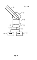
図1は、本発明のある実施形態による、全ソリッドステート光学伝送/受信端末100の概略図である。レンズ102が、光線106によって表される入射光線が光学スイッチネットワーク104の表面107上に合焦されるように、(本明細書では「光導波管ネットワーク」または「光学スイッチ」とも称される)光学スイッチネットワーク104に光学的に結合される。逆に、光学スイッチネットワーク104の表面107において放出される光学信号は、レンズに光学的に結合され、それによって、光線106として空間の中に投影される。光は、赤外線(IR)等の、人間に視認可能または視認不可能であり得る。表面107は、平面状の表面または非平面状の表面であってもよい。
FIG. 1 is a schematic view of an all-solid-state optical transmission /
レンズ102は、好ましくは、広視野レンズである。レンズ102は、例えば、屈折率分布(GRIN)レンズ、魚眼レンズ、または単心レンズであってもよい。好適な単心レンズは、Distant Focus Corporation(PO Box 7857, Champaign, IL 61826−7857)から入手可能である。レンズが、平面状の集束された画像を作成する場合、レンズ102および光学スイッチネットワーク104は、空気または真空108によって光学的に結合されてもよい。しかしながら、レンズが湾曲した集束された画像を作成する場合、光ファイバ108の束が、レンズ102を光学スイッチネットワーク104に光学的に結合するために使用されてもよい。光ファイバ108の束の各光ファイバの1つの端部が、レンズ102の表面上で終端してもよく、光ファイバの他の端部が、光学スイッチネットワーク104の表面107上で終端してもよい。レンズ102の表面上で終端する光ファイバ108の端部は、研磨された端部を有し、レンズ102の湾曲に合致する湾曲した表面を形成してもよい。
The
図2は、図1の光学スイッチネットワーク104の表面107上の、ポート202、204、206、208、および210によって表される複数のN個のポート200を図示する、概略図である。複数のポート200は、長方形アレイ内に配置されるものとして示される。しかしながら、ポート200は、任意の好適な配列内に配列されてもよい。光ファイバ108(図1)が、レンズ102を光学スイッチネットワーク104に結合するために使用される場合、1つ以上の光ファイバ108が、各ポート202−210において終端してもよい。光ファイバ108は、レンズ102によって投影された画像が複数のポート200内の対応する場所にマッピングされるように配列されるべきである。したがって、各ポート202−210は、レンズ102の視野の一意の部分に対応する。
FIG. 2 is a schematic diagram illustrating a plurality of
図1に戻ると、光学スイッチネットワーク104はまた、単一の共通入力/出力ポート110を有する。光学スイッチネットワーク104は、表面107上のN個のポート202−210(図2)のうちの1つ以上のものを共通入力/出力ポート110に選択的に光学的に結合するように構成される。したがって、1つのモードにおいて、光学スイッチネットワーク104は、N×1スイッチとして作用する。すなわち、N個のポート202−210のうちの1つが、共通入力/出力ポート110に結合される。随意に、他のモードにおいて、光学スイッチネットワーク104は、複数のN×1スイッチとして作用する。すなわち、複数のN個のポート202−210が、共通入力/出力ポート110に同時に結合される。
Returning to FIG. 1, the
端末100はまた、フォトダイオード等の好適な光学受信機112および/またはレーザ等の好適な伝送機114を含む。LiDARシステムまたは双方向通信システムは、伝送機114と、受信機112との両方を含む。しかしながら、単方向通信システムは、伝送機114または受信機112のみを含む必要があり、スタートラッカは、受信機112のみを含む必要がある。受信機112および/または伝送機114は、光ファイバ、鏡、および/または分割器/結合器等の光学結合器116によって表される好適な光学結合器によって、共通入力/出力ポート110に光学的に結合される。
The terminal 100 also includes a suitable
したがって、伝送機114からの光学信号が、光学結合器116を介して光学スイッチネットワーク104にルーティングされ、そこで、N個のポート202−210のうちの選択される1つ以上のものに切り替えられてもよい。いったん光学スイッチ107の表面107から放出されると、光学信号は、選択されるポート202−210において終端される光ファイバ108等を介して、レンズ102に伝達され、次いで、レンズ102によって空間の中に伝達される。光学信号がレンズ102によって投影される空間における方向は、選択されるポート202−210に依存する。逆に、LiDARシステムにおける帰還信号等の、レンズ102によって受信される光学信号が、光学スイッチネットワーク104によって受信機112にルーティングされる。光学信号がレンズ102によって受信される空間における方向は、選択されるポート202−210に依存する。
Thus, the optical signal from the transmitter 114 is routed to the
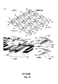
図3は、本発明のある実施形態による、光学スイッチネットワーク104を図示する、概略図である。図3の右側は、共通入力/出力ポート110においてルートされた光導波管の「Hツリー」配列(分岐した光導波管ネットワーク)を示す。図3の左側は、拡大された右側の一部を示す。ポート202−210が、図3に示される。
FIG. 3 is a schematic diagram illustrating an
バイナリ光学スイッチは、バイナリ光学スイッチ300、302、304、306、308、および310によって例示されるように、Hツリーの2つの光導波管の各接合部に配置される。バイナリ光学スイッチは、2つの光学経路のうちのいずれかに沿って光学信号をルーティングする。したがって、バイナリ光学スイッチ300−308は、Hツリーを通して進行する光学信号のための道筋を決定する。いくつかの実施形態では、バイナリ光学スイッチは、2つの光学経路のうちの多くとも一方に沿って光学信号をルーティングする。例えば、光学信号が共通入力/出力ポート110の中に導入される場合、バイナリ光学スイッチ300−308は、光学信号をN個のポート202−210のうちの1つにルーティングする。図3に描写される実施例では、光学信号は、ポート202にルーティングされる。
The binary optical switch is located at each junction of the two optical waveguides in the H tree, as exemplified by the binary
いくつかの実施形態では、各バイナリ光学スイッチは、マッハツェンダー干渉計を伴って実装される。そのようなバイナリ光学スイッチ400の実施例が、図4に図式的に図示される。入力部402における光が、2つの経路404と406との間で分割される。位相偏移器408および/または410は、経路404および406の一方または両方上で選択的にイネーブルにされ、次いで、光が、2×2型結合器412によって再結合される。2つの経路404および406内の光の相対的位相は、光が、2×2型結合器412の第1の出力部414または第2の出力部416または両方の出力部414および416に結合するかどうかを決定する。位相偏移器408および410は、MEMSデバイスまたは任意の他の好適な位相偏移器による電気光学または熱光学効果を使用して実装されてもよい。
In some embodiments, each binary optical switch is implemented with a Mach-Zehnder interferometer. An embodiment of such a binary
代替として、バイナリ光学スイッチ300−310は、リング共振器、MEMS鏡等の微小電気機械システム(MEMS)デバイス、または任意の他の好適なバイナリ光学スイッチを伴って実装されてもよい。 Alternatively, the binary optical switch 300-310 may be implemented with a microelectromechanical system (MEMS) device such as a ring resonator, a MEMS mirror, or any other suitable binary optical switch.
光学スイッチネットワーク104は、Hツリーパターン内に配列されるバイナリ光学スイッチ300−310のネスト化されたアレイを含む。アレイのネスト化された性質は、バイナリ光学スイッチ300−310のL個の層が2L個の可能性として考えられるポート200の間で選択するために使用され得ることを意味する。したがって、アクティブなバイナリ光学スイッチの数は、Nの代わりに、log2(N)である(但し、Nは、ポート200(可能性として考えられるビーム方向)の数である)。
The
図3に見られ得るように、光学信号を共通入力/出力ポート110から選択されるポート202にルーティングするために、Hツリーにおけるリーフの数、すなわち、ポート200の数と比較して、比較的に少数のバイナリ光学スイッチ300−310が、動作される、すなわち、オンである必要がある。例えば、図3の左側では、6個のスイッチ、すなわち、3個の左/右バイナリ光学スイッチ300、304、および308、および3個の上/下バイナリ光学スイッチ302、306、および310が、64個の可能性として考えられるポート200のうちのいずれかの選択を可能にする。大部分の実施形態では、所与のレベルの1つのスイッチのみが、一度に動作される。本少数のスイッチが、したがって、匹敵する光学位相アレイ内の位相偏移器よりはるかに少ないエネルギーを消費する。加えて、バイナリ光学スイッチ300−310は、単に、双レベル状態において動作する必要があるのに対し、位相アレイは、操向のために位相偏移器の任意制御を必要とする。さらに、これらの実施形態は、広帯域光に好適であり、複数のチャネルが波長分割多重を使用して一度に送信および/または受信されることを可能にする。
As can be seen in FIG. 3, in order to route the optical signal to the
光学スイッチネットワーク104は、光導波管のHツリー配列を含むものとして説明されるが、バイナリ光学スイッチのネスト化されたアレイを提供する、任意の好適な分岐した光導波管ネットワークもまた、使用され得る。例えば、他のフラクタル配列および非フラクタル配列もまた、使用され得る。本明細書で使用されるように、「フラクタル」は、異なる縮尺を横断する自己相似を意味する。本明細書で使用されるように、フラクタルパターンは、際限なく複雑ではない。
(バイナリ光学スイッチのアドレス指定)
Although the
(Addressing of binary optical switch)
バイナリ光学スイッチ300−310は、図5に図式的に示されるように、行および列アドレス指定行列500等の任意の好適な配列によってアドレス指定および/または作動されてもよい。各バイナリ光学スイッチ300−310は、バイナリ光学スイッチが電気的に結合される、個別の2入力部ANDゲートによって作動されてもよい。ANDゲートは、バイナリ光学スイッチ300−310のパターンと位置合わせするパターン内に配列されてもよい。ANDゲート502、504、506、508、510、および512によって表される図5のANDゲートは、図3のバイナリ光学スイッチ300−310と位置合わせする。ANDゲート502は、バイナリ光学スイッチ300と位置合わせし、ANDゲート504は、バイナリ光学スイッチ302と位置合わせする等となる。
The binary optical switch 300-310 may be addressed and / or actuated by any suitable sequence, such as the row and
各ANDゲートは、行ワイヤ514、516、および518および列ワイヤ520、522、および524によって表される、対応する行ワイヤおよび対応する列ワイヤの交点に配置される。各ANDゲートの1つの入力部が、ANDゲートの対応する行ワイヤに電気的に結合され、ANDゲートの他の入力部が、ANDゲートの対応する列ワイヤに電気的に結合される。したがって、1つの行上の論理「1」(真)信号および1つの列上の論理「1」(真)信号は、ANDゲートのうちの1つを一意にイネーブルにし、イネーブルにされたANDゲートは、個別のバイナリ光学スイッチを作動させる。
Each AND gate is located at the intersection of the corresponding row wire and the corresponding column wire, represented by
いったん作動されると、バイナリ光学スイッチは、所定量の時間にわたって作動されたままであり得る。随意に、または代替として、いったん作動されると、バイナリ光学スイッチは、バイナリ光学スイッチがリセット信号を受信するまで作動されたままであり得る。リセットライン(図示せず)が、バイナリ光学スイッチ300−310の全てへと延在し、作動されたバイナリ光学スイッチ300−310の全ての同時リセットを促進してもよい。バイナリ光学スイッチのリセットは、下記により詳細に議論される。 Once activated, the binary optical switch can remain activated for a predetermined amount of time. Optionally, or as an alternative, once activated, the binary optical switch may remain activated until the binary optical switch receives a reset signal. A reset line (not shown) may extend to all of the binary optical switches 300-310 to facilitate all simultaneous resets of the activated binary optical switches 300-310. Resetting the binary optical switch is discussed in more detail below.
行および列アドレス指定行列500は、共通入力/出力ポート110とN個のポート200の選択されるポートとの間のHツリーを通して、所望される光学経路に沿って存在するバイナリ光学スイッチ300−310のうちの選択されるものを連続的に作動させるために使用されてもよい。すなわち、行および列アドレス指定行列500が、使用され、バイナリ光学スイッチ300−310の第1のものを作動させ、次いで、第1のバイナリ光学スイッチがリセットする前に、行および列アドレス指定行列500が、使用され、Hツリーを通して所望される光学経路に沿って存在する、選択されるバイナリ光学スイッチ300−310の全てが作動されるまで、バイナリ光学スイッチ300−310のうちの第2の(異なる)もの等を作動させてもよい。
The row and
各作動されたバイナリ光学スイッチは、光を指向する方向に関する命令を受信する必要がある。この目的のために、各バイナリ光学スイッチ300−310はまた、付加的な類似した行および列アドレス指定行列(図示せず)に結合されてもよい、または行および列行列500は、時分割多重方式における付加的な行列としての役割を果たしてもよい。付加的な類似した行および列アドレス指定行列は、共通入力/出力ポート110からの光学信号を選択されるポート202にルーティングするために、光を1つの方向、例えば、「左」に指向するべき各作動されたバイナリ光学スイッチに信号を送信するために使用されてもよい。本「左」信号を受信しない作動されたバイナリ光学スイッチは、それらが光を反対方向、例えば、「右」に指向することになると考えて差し支えない。
Each activated binary optical switch needs to receive a command regarding the direction in which the light is directed. For this purpose, each binary optical switch 300-310 may also be coupled to an additional similar row and column addressing matrix (not shown), or the row and
作動されたバイナリ光学スイッチが、それらの個別のコマンドされた方向に切り替えるための時間を経た後、共通入力/出力ポート110が、選択されるポート202と光学通信し、受信機112および/または伝送機114が、動作してもよい。受信機112および/または伝送機114は、一定の時間周期にわたって、または異なる方向の光線106が必要とされるまで動作してもよい。
After the activated binary optical switches have passed the time to switch in their individual commanded directions, the common input /
伝送および/または受信が完了した後、または所定の時間周期の後等、光学スイッチネットワーク104を通した異なる光経路が必要とされるとき、または異なる方向の光線106が必要とされるとき、バイナリ光学スイッチ300−310が、リセットされる。記載されるように、バイナリ光学スイッチは、光学スイッチネットワーク104を通した所望される光学経路を確立し、光学信号を送信および/または受信するために必要とされるバイナリ光学スイッチの全てを作動させるために十分な量の時間等の所定の量の時間にわたって、作動されたままであってもよい。随意に、または代替として、作動されたバイナリ光学スイッチは、上記に説明されるリセット信号によってリセットされてもよい。
Binary when different optical paths through the
別の好適なそのような行および列アドレス指定行列600が、図6に図式的に示されるが、単純化のために、行列600は、正方形の行列として示される。行列600の行は、行602、604、および606によって例示され、行列600の列は、列608、610、および612によって例示される。トランジスタ614、616、および618によって第1の行602内に表される個別のトランジスタは、第1の行602を列608−612に選択的に電気的に結合する。電圧が、第1の行602に印加され、それによって、電流を第1の行602内に流動するように利用可能にする。したがって、囲繞する円によって示されるようなオンであるトランジスタ618等の第1の行のトランジスタは、電流を、太矢印620によって示されるような選択される列、この場合、列612に指向する。
Another suitable row and
各列において、個別のトランジスタは、列を、対応するバイナリ光学スイッチ(図6に図示せず)に結合させる。囲繞する円によって示されるようなオンであるトランジスタ622等の、給電された列612におけるトランジスタは、電気的に結合され、電流を、その対応するバイナリ光学スイッチに指向し、それによって、バイナリ光学スイッチをアクティブ化する。
In each row, a separate transistor couples the row to a corresponding binary optical switch (not shown in FIG. 6). Transistors in the fed
代替として、アドレス指定を容易にするために、トランジスタの行502−506全体が、追加のトラジスタをオンにするために使用される追加の電力以外の本デバイス動作に影響を及ぼすことなく、同時にオンにされることができる。トランジスタは、直接的に、または、例えば、シフト演算子の使用によってアクティブ化されることができる。 Alternatively, to facilitate addressing, the entire row 502-506 of the transistor is turned on at the same time without affecting the operation of the device other than the additional power used to turn on the additional transistor. Can be made. Transistors can be activated either directly or, for example, by using shift operators.
図1に戻ると、レンズ102は、全ソリッドステート光学伝送/受信端末100の、位相偏移要素の数から開口のサイズを結合解除することによって、非常に大きい有効口径面積、したがって、電力消費量を可能にする。2次元または3次元空間におけるビームの出力を制御するための平面チップにおける光学スイッチネットワーク内でバイナリ光学スイッチを使用することが、本開示の新規の側面を表す。同様に、そのようなチップからビームを外に指向するためにレンズ102を使用することもまた、本開示の新規の側面を表す。
(粗密ハイブリッド)
Returning to FIG. 1, the
(Dense hybrid)
いくつかの用途は、広い視野にわたる光ビームの非常に細かい位置付けを要求する。50万個もの1つの部品を各方向に位置付けることの要件は、前代未聞である。上記に説明されるような実施形態に別の位置付けスキームを追加するハイブリッドアプローチは、そのような大きいダイナミックレンジを達成することができる。本ハイブリッドアプローチは、広い視野にわたる細かい位置付けの問題を、2つの別個の問題、すなわち、粗い位置付け制御の1つのものと、細かい位置付け制御の他のものとに分割する。 Some applications require very fine positioning of the light beam over a wide field of view. The requirement to position as many as 500,000 single parts in each direction is unheard of. A hybrid approach that adds another positioning scheme to the embodiments as described above can achieve such a large dynamic range. This hybrid approach divides the fine positioning problem over a wide field of view into two separate problems: one for coarse positioning control and another for fine positioning control.
一実施形態では、粗い位置付け制御は、光学伝送/受信端末100を使用して、すなわち、上記に説明されるような光学スイッチネットワークを使用して達成され得、細かい制御は、図7に図式的に図示されるように、レンズ102を光学スイッチネットワーク104に対して物理的に偏移させることによって、または図17に図式的に図示されるように、光学スイッチネットワーク104をレンズ102に対して物理的に偏移させることによって達成され得る。例えば、図7に示されるように、レンズ102は、x−y段700上に搭載されてもよい、または図17に示されるように、光学スイッチネットワーク104は、x−y段800上に搭載されてもよい。代替として、図9に図式的に示されるように、粗い制御は、x−y段900等によって光学スイッチネットワーク104とともにレンズ102を物理的に偏移することによって達成され得、光学伝送/受信端末100内の光学スイッチネットワークは、細かく急速なビーム移動を達成するために使用されてもよい。
In one embodiment, coarse positioning control can be achieved using the optical transmission /
代替として、図10に図式的に図示されるように、小型レンズアレイ等の中間光学系1000が、レンズ102と光学スイッチネットワーク104のポート200との間に光学的に配置されてもよく、中間光学系1000は、x−y段(図示せず)等によって物理的に偏移されてもよい。小型レンズアレイは、ポート200のポート毎に1つの小型レンズを含んでもよい。小型レンズ1002によって表される、小型レンズアレイの各小型レンズは、その偏移されていない位置において、ポート200のポート1004によって表される、対応するポートの中心上に位置合わせするはずである。
Alternatively, as illustrated graphically in FIG. 10, an intermediate
例えば、矢印1006によって示されるような中間光学系1000の偏移は、ポート1004とレンズ102との間の光ビームを矢印1008によって示されるように偏移させ、これは、レンズ102によって放出または受光される光ビームを、矢印1010によって示されるように、自由空間にまたはそこから偏移させる。中間光学系1000は、走査され、それによって、ラスタ走査を実施する等のために光線106を走査してもよい。
For example, a shift of intermediate
中間光学系1000として使用される小型レンズの単一のアレイが、転向角において限定され得、収差をもたらし得る。図11に図式的に示されるような小型レンズアレイ1100、1102、および1104によって例示される小型レンズのいくつかのアレイが、光学スイッチネットワーク104に続いて直列に配置され、これらの課題を克服し得る。この場合、レンズ102は、光学スイッチネットワーク104から最も遠くに光学的に配置される、小型レンズアレイ1102および1104等の小型レンズアレイのうちの1つ以上のものによって置換されてもよい。小型レンズアレイ1100−1102のうちの2つ以上のものが、個別のx−y段(図示せず)等によって別個に、光線106を偏移させるまたは走査するように物理的に偏移されてもよい。図11に示される実施形態では、最後の2つの小型レンズアレイ1102および1104が、単一のx−y段等によってともに偏移される。
A single array of small lenses used as intermediate
代替として、中間光学系1000は、x−y段等によって偏移可能であって、かつその偏移範囲全体を通して、光学スイッチネットワーク104のポート200の全てとレンズ102との間の場の全体を光学的に包含するために十分に大きい、単一の大きいレンズ(図示せず)を含んでもよい。
(複数のビーム)
As an alternative, the intermediate
(Multiple beams)
上記に説明される実施形態では、バイナリ光学スイッチ300−310が、1つの経路または別のものを辿って光を完全に指向する。他の実施形態では、いくつかまたは全てのバイナリ光学スイッチが、Hツリーを通して1つを上回る経路の間で光を均一または任意に分割し、複数のビーム106を異なる方向に同時に指向することを可能にする。各レベルにおける複数のスイッチが、アドレス指定される必要があるため、これを達成するために、好適な変更が、本明細書に説明されるバイナリ光学スイッチおよびアドレス指定スキームに行われる。
(導波管の内部および外部に光を選択的に結合するための統合MEMSスイッチ)
In the embodiments described above, the binary optical switch 300-310 follows one path or another to completely direct the light. In other embodiments, some or all binary optical switches can uniformly or arbitrarily split the light between more than one path through the H-tree, directing
(Integrated MEMS switch for selectively coupling light inside and outside the waveguide)
バイナリ光学スイッチ300−310が加工され得る密度に対する限定が、伝送/受信端末100の空間分解能、すなわち、可能性として考えられる伝送または受信ビーム位置の密度を限定し得る。図12は、本発明の別の実施形態による、光学スイッチネットワーク104(図1)に取って代わり得る光学スイッチネットワーク1200を図示する、概略図である。光学スイッチネットワーク1200は、上記に説明される光学スイッチネットワーク104より高いスイッチ密度を提供し得る。本実施形態では、光学スイッチネットワークは、光学ビームを操向するために、MEMSベースのバイナリ光学スイッチを採用する。
Limitations on the density at which the binary optical switch 300-310 can be machined can limit the spatial resolution of the transmission /
MEMSベースのバイナリ光学スイッチは、Hツリーベースのバイナリ光学スイッチ300−310より有意に小さくあり得る。その結果、MEMSベースのバイナリ光学スイッチは、先行技術におけるものより高い密度で加工または充塞され、伝送/受信端末のより高い空間分解能、すなわち、可能性として考えられる伝送/受信ビーム位置の密度を提供し得る。全ソリッドステート光学伝送/受信端末100と同様に、MEMSベースのスイッチの比較的に小さいサブセットが、任意の所与の時間において動作され、したがって、給電される必要がある。したがって、光学スイッチネットワーク1200を含む端末は、先行技術と関連付けられる、機械的なスイッチ密度、エミッタ密度、および高電力問題を克服する。
MEMS-based binary optical switches can be significantly smaller than H-tree-based binary optical switches 300-310. As a result, MEMS-based binary optical switches are machined or filled with higher densities than those in the prior art, providing higher spatial resolution of transmission / reception terminals, i.e., potentially possible transmission / reception beam position densities. Can be done. Similar to the All Solid State Optical Transmission / Receiving
光学スイッチネットワーク1200は、共通入力/出力ポート1202を含む。光は、両矢印1204によって示されるように、共通入力/出力ポート1202に進入および/またはそれから退出し得る。共通入力/出力ポート1202は、第1の光導波管1206に光学的に結合される。光学スイッチネットワーク1200はまた、光導波管1208、1210、1212、1214、および1216によって表される、複数の第2の光導波管を含む。各第2の光導波管1208−1216は、第1のバイナリ光学スイッチ1218、1220、1222、1224、および1226によって表される、個別の第1のバイナリ光学スイッチを介して、第1の光導波管1206に光学的に結合される。
The
いくつかの実施形態では、各第1のバイナリ光学スイッチ1218−1226が、単極双投(SPDT)スイッチとして作用する。したがって、光が共通入力/出力ポート1202に進入すると仮定して、第1のバイナリ光学スイッチ1218は、光が第1の光導波管1206に沿って継続することを可能にするか、または光を第2の光導波管1208に転向させるかのいずれか一方を選択的に行うが、両方は行わない。したがって、集合的に、第1のバイナリ光学スイッチ1218−1226は、光がどの第2の光導波管1208−1216に転向されるかを制御する。同様に、集合的に、第1のバイナリ光学スイッチ1218−1226は、受信モードにおいて、光が、どの第2の光導波管1208−1216から第1の光導波管1206に、そしてそこから共通入力/出力ポート1202にルーティングされるかを制御する。5個の第2の光導波管1208−1216および5個の第1のバイナリ光学スイッチ1218−1226が示されるが、任意の好適な数の第2の導波管および第1のバイナリ光学スイッチが、含まれてもよい。
In some embodiments, each first binary optical switch 1218-1226 acts as a unipolar double throw (SPDT) switch. Thus, assuming light enters the common input /
第2のバイナリ光学スイッチ1228、1230、1232、1234、1236、1238、1240、および1242によって表される、個別の複数の第2のバイナリ光学スイッチが、各第2の光導波管1208−1216に光学的に結合される。例えば、第2のバイナリ光学スイッチ1228−1232が、第2の光導波管1208に光学的に結合される。各第2のバイナリ光学スイッチ1228−1242が、個別の第2の光導波管1208、1210、1212、1214、または1216を自由空間に選択的に光学的に結合してもよい。第2のバイナリ光学スイッチ1228−1242が、第2の光導波管1208−1216とN個のポート202−210(図2)との間で結合されてもよい、または各第2のバイナリ光学スイッチ1228−1242が、N個のポート202−210のうちの1つの一部または全体を形成してもよい。
A plurality of individual second binary optical switches, represented by the second binary
いくつかの実施形態では、各第2のバイナリ光学スイッチ1228−1242が、単極双投(SPDT)スイッチとして作用する。したがって、光が共通入力/出力ポート1202に進入し、破線1244によって示されるように、第1のバイナリ光学スイッチ1222によって第2の光導波管1212にルーティングされると仮定して、第2のバイナリ光学スイッチ1238が、光が第2の光導波管1212に沿って継続することを可能にするか、または光を、両矢印1246によって示されるように、第2の光導波管1212から外に転向させるかのいずれか一方を選択的に行う。両矢印1246は、図面の平面から外に延在する。したがって、集合的に、第2のバイナリ光学スイッチ1228−1242は、光が、N個のポート202−210のうちのどのポートに転向されるかを制御する。同様に、集合的に、第2のバイナリ光学スイッチ1228−1242は、受信モードにおいて、光が、N個のポート202−210のうちのどのポートから第1の光導波管1206に、そしてそこから共通入力/出力ポート1202にルーティングされるかを制御する。
In some embodiments, each second binary optical switch 1228-1242 acts as a unipolar double throw (SPDT) switch. Therefore, assuming that light enters the common input /
14個の第2のバイナリ光学スイッチが、各第2の光導波管1208−1216に結合されて示されるが、任意の数の第2のバイナリ光学スイッチが、含まれてもよい。第2の光導波管322−1242の全てが、等しい数の第2のバイナリ光学スイッチ1228−1242を有する必要はない。 Fourteen second binary optical switches are shown coupled to each second optical waveguide 1208-1216, although any number of second binary optical switches may be included. Not all of the second optical waveguides 322-1242 need to have an equal number of second binary optical switches 1228-1242.
各第1および第2のバイナリ光学スイッチ1218−1226および1228−1242が、バイナリであり、すなわち、厳密に2つの位置または状態を有する、オン/オフまたは他のスイッチである。したがって、第1および第2のバイナリ光学スイッチ1218−1226および1228−1242は、例えば、破線1244によって例示されるように、共通入力/出力ポート1202とN個のポート202−210のうちの選択されるポートとの間のスイッチアレイ1200を通して進行する光学信号のための光学経路を決定する。
Each of the first and second binary optical switches 1218-1226 and 1228-1242 is binary, i.e. on / off or other switch having exactly two positions or states. Therefore, the first and second binary optical switches 1218-1226 and 1228-1242 are selected from the common input /
各第1のバイナリ光学スイッチ1218−1226は、任意の好適な光学スイッチによって実装されてもよい。いくつかの実施形態では、各第1のバイナリ光学スイッチ1218−1226は、MEMSによって作動される断熱性光学結合器の対によって実装される。そのようなスイッチセルが、2016年1月のTae Joon Seok, et al.の「Large−scale broadband digital silicon photonic switches with vertical adiabatic couplers」Optica, Vol. 3, No. 1, pp. 64−70(「Seok」)およびTae Joon Seok, et al.の「Large−scale broadband digital silicon photonic switches with vertical adiabatic couplers: supplemental material」(「Seok補遺」)(その内容全体は、全ての目的のために、参照することによって本明細書によって本明細書に組み込まれる)において説明される。各第1のバイナリ光学スイッチ1218−1226は、2つの光導波管を使用して実装されてもよい。しかしながら、Seokにおいて説明されるものとは異なり、2つの導波管は、交差する必要はなく、スイッチの主要部のみが、類似している。MEMSによって作動される断熱性結合器の対を含むスイッチ要素は、2つの光導波管の間に光学的に配置されてもよい。例えば、Seokの(本願において、図13として注釈を伴って複製される)図1を参照されたい。 Each first binary optical switch 1218-1226 may be implemented by any suitable optical switch. In some embodiments, each first binary optical switch 1218-1226 is implemented by a pair of adiabatic optical couplers operated by MEMS. Such a switch cell is described in Tae Joon Seok, et al., January 2016. "Large-scale broadband digital silicon photonics with vertical adiabatic couplers" Optica, Vol. 3, No. 1, pp. 64-70 (“Sok”) and Tae Joon Seok, et al. "Large-scale broadband digital silicon photonic switchs with virtual adiabatic couplers: supplemental material by supplemental material" (incorporated herein by reference in its entirety, by reference to the specification in its entirety). Is explained in). Each first binary optical switch 1218-1226 may be implemented using two optical waveguides. However, unlike those described in Seek, the two waveguides do not need to intersect, only the main part of the switch is similar. The switch element, including the pair of adiabatic couplers operated by MEMS, may be optically located between the two optical waveguides. See, for example, FIG. 1 of Seek (reproduced with annotation as FIG. 13 in the present application).
オフ状態(図13c)では、断熱性結合器1300および1302によって例示される断熱性結合器が、光導波管1306および1308によって例示される、光導波管の約1μm上方等、十分に離れて位置1304し、したがって、光が、他の導波管1308に感知できるように結合することなく、(「スルー」によって示されるように)導波管1306のうちの1つに沿って伝搬し続ける。しかしながら、オン状態(図13d)では、断熱性結合器1300および1302が、MEMS静電ギャップ閉鎖アクチュエータによって導波管1306および1308に向かって物理的に移動され、光は、したがって、導波管1306のうちの1つから断熱性結合器1300のうちの1つの中へ、そして(「ドロップ」によって示されるように)他の断熱性の結合器1302と他の導波管1308との間で効率的に結合される。
In the off state (FIG. 13c), the adiabatic couplers exemplified by the
代替として、各第1のバイナリ光学スイッチ1218−1226(図12)は、図4に関して上記で議論されるように、例えば、熱位相偏移器を伴う標準的なマッハツェンダー干渉計タイプスイッチを使用して実装されてもよい。 As an alternative, each first binary optical switch 1218-1226 (FIG. 12) uses, for example, a standard Mach-Zehnder interferometer type switch with a thermal phase shifter, as discussed above with respect to FIG. May be implemented.
記載されるように、光学スイッチネットワーク104の表面107(図1)は、N個のポート202−210を有し、レンズ102は、入射光線106をN個のポート202−210上に合焦させ、および/またはレンズ102は、N個のポート202−210の任意のサブセットを介して放出される光学信号を空間の中に投影する。光学格子は、両矢印1246(図12)によって示されるように、第2の光導波管1208−1216の平面から外に光を放出する、または第2の光導波管1208−1216の中に面外の光を結合するための効率的なデバイスである。光学格子は、異なる第2の屈折率を有する領域が散在される第1の屈折率を有する複数の領域を画定する、空間的に周期的な構造である。空間周期は、着目波長に基づいて選択される。ある場合には、周期的な溝が、材料内で画定される。他の場合では、異なる屈折率を有する2つの異なる材料が、互い違いにされる。説明の単純化のために、用語「溝」は、実際の溝、すなわち、空所、または光学格子の2つの互い違いにされた材料のうちの1つを表すために本明細書において使用される。
As described, the surface 107 (FIG. 1) of the
そのような光学格子は、表面107(図1)またはその近傍に配置されてもよい。各第2のバイナリ光学スイッチ1228−1242(図12)は、そのような光学格子を含んでもよい。特に、各第2のバイナリ光学スイッチ1228−1242は、物理的に平行移動可能な光学格子、すなわち、少なくとも2つの位置の間で物理的に平行移動するように構成される光学格子によって実装されてもよい。第1の(「オン」)位置では、光学格子は、ある着目波長において、少なくとも約25%の結合効率を伴って第2の光導波管に光学的に結合するように、第2の光導波管1208−1216のうちの1つに十分に近接している。第2の(「オフ」)位置では、光学格子は、ある着目波長において、多くとも約5%、好ましくは、1%未満の結合効率を伴って第2の光導波管に光学的に結合するように、第2の光導波管から十分に離れている。図12は、第2のバイナリ光学スイッチ1228−1242のうちの3つを拡大された状態で1244に示す。 Such an optical grid may be arranged at or near the surface 107 (FIG. 1). Each second binary optical switch 1228-1242 (FIG. 12) may include such an optical grid. In particular, each second binary optical switch 1228-1242 is implemented by a physically translatable optical grid, i.e., an optical grid configured to physically translate between at least two positions. May be good. In the first (“on”) position, the optical grid has a second optical waveguide such that it optically couples to the second optical waveguide with a coupling efficiency of at least about 25% at a wavelength of interest. Close enough to one of the tubes 1208-1216. In the second (“off”) position, the optical grid optically couples to the second optical waveguide with a coupling efficiency of at most about 5%, preferably less than 1%, at a wavelength of interest. As such, it is sufficiently far from the second optical waveguide. FIG. 12 shows three of the second binary optical switches 1228-1242 in an enlarged state at 1244.
各第2のバイナリ光学スイッチ1228−1242は、平行移動可能な光学格子をオン位置およびオフ位置に選択的に平行移動させるように構成される、MEMS構造を含んでもよい。図14は、第2のバイナリ光学スイッチ1228−1242のうちの1つのバイナリ光学スイッチ1400の概略上面図である。バイナリ光学スイッチ1400は、平行移動可能な格子1402を含む。平行移動可能な格子1402は、複数の平行または略平行な周期的な溝を画定する。溝は、壁1404、1406、および1408によって表される壁によって分離される。記載されるように、溝および壁は、異なる屈折率を有する個別の材料によって実装されてもよい。壁1404−1408は、従来の半導体加工技法を使用して、シリコン、窒化ケイ素、または別の好適な材料から作製されてもよい。溝は、空所である、または壁1404−1408と異なる好適な材料から作製されてもよい。平行移動可能な格子1402が、6つの壁1404−1408を伴って示されるが、任意の好適な数の壁および/または溝が、使用されてもよい。平行移動可能な格子1402が、第2の光導波管1410、すなわち、第2の光導波管1208−1216(図12)のうちの1つの上方に配置される。
Each second binary optical switch 1228-1242 may include a MEMS structure configured to selectively translate a translatable optical grid into on and off positions. FIG. 14 is a schematic top view of one of the second binary optical switches 1228-1242, the binary
図15は、オフ位置における、バイナリ光学スイッチ1400の概略側面図である。オフ位置では、平行移動可能な光学格子1402が、多くとも約5%、好ましくは、1%未満、そしていくつかの実施形態では、0.1%未満の結合効率を伴って、第2の光導波管1410に光学的に結合するために十分である、第2の光導波管1410からの距離1500をおいて配置される。いくつかの実施形態では、距離1500は、約1μm(1,000nm)である。いくつかの実施形態では、距離1500は、約800nmであってもよい。いくつかの実施形態では、距離1500は、約250nmであってもよい。オフ位置では、第2の光導波管1410内の大部分または実質的に全ての光1502が、矢印1504によって示されるように、第2の光導波管1410に沿って継続する。同様に、自由空間から光学格子1402を介して第2の光導波管1410の中に結合する光は、非常に少ない、または実質的に存在しない。
FIG. 15 is a schematic side view of the binary
第2の光導波管1410が、従来の半導体加工技法を使用して、シリコンまたは窒化ケイ素ウエハ等の好適な半導体ウエハ上に加工されてもよい。第2の光導波管1410は、好適な酸化物または他の不動態化層1506上に加工されてもよい。
The second
図16は、オン位置における、バイナリ光学スイッチ1400の概略側面図である。オン位置では、平行移動可能な光学格子1402が、少なくとも約25%の結合効率を伴って第2の光導波管1410に光学的に結合するために十分である、第2の光導波管1410からの距離1600をおいて配置される。いくつかの実施形態では、距離1600は、約10〜50nmである。オン位置では、第2の光導波管1410内のより多く、大部分、または実質的に全ての光1502が、矢印1602によって示されるように、平行移動可能な光学格子1402によって自由空間の中に放出される。同様に、自由空間からの好適なモードのより多く、大部分、または実質的に全ての光が、光学格子1402を介して第2の光導波管1410の中に結合する。
FIG. 16 is a schematic side view of the binary
図17は、本発明のある実施形態による、代表的な寸法を示す、オン位置におけるバイナリ光学スイッチ1400の別の概略側面図である。平行移動可能な格子1402が、第2の光導波管1410から約20nmの距離(D)をおいて配置される。第2の光導波管1410は、約150nmの厚さ(T)のシリコン・オン・オキサイド基板1506である。入力光ビーム1502は、約2.5μmの半径を伴うガウスビームである。平行移動可能な格子1402は、約50nmの厚さ(H)を有する。平行移動可能な格子1402は、約580nmの溝周期(Λ)を有する。光の他の波長の溝周期(Λ)を変更する等の適切な修正が、当業者によって公知であろうように、成され得る。
FIG. 17 is another schematic side view of the binary
図14−16に関して議論されるように、各第2の光学スイッチ1228−1242は、平行移動可能な光学格子1402をオン位置およびオフ位置に選択的に平行移動させるように構成される、MEMS構造を含んでもよい。図18および19は、平行移動可能な光学格子1400をオン位置およびオフ位置に選択的に平行移動させるように構成される静電MEMS構造1800を示す、オフ位置における光学スイッチ1400の個別の概略斜視図および側面図である。図20は、オン位置における光学スイッチ1400の概略斜視側面図である。平行移動可能な光学格子1402が、破線の楕円1802内に示されている。
As discussed with respect to FIG. 14-16, each second optical switch 1228-1242 is configured to selectively translate the translatable
平行移動可能な光学格子1402は、ブリッジ1804の一部である。ブリッジ1804は、基板1506から離間され、かつその上方に配置される。基板1506は、埋設された酸化物層1900(図19および20)を含んでもよい。ブリッジ1804は、個別のピア1808および1810によって支持される。第2の光導波管1410は、平行移動可能な光学格子1402の下の基板1506内またはその上に配置される。
The translating
ブリッジ1804は、2つの第1の静電作動電極1812および1814を含む。2つの対応する第2の静電作動電極1816および1818は、2つの第1の作動電極1812および1814が、それぞれ、2つの第2の作動電極1816および1818にわたって位置合わせするように、基板1506上に配置される。ブリッジ1804はまた、2つの撓曲部1820および1822を含む。
The
したがって、電位2000が、図20に図式的に示されるように、第1および第2の作動電極1812−1814および1816−1818を横断して印加される場合、結果として生じる静電力が、第1の作動電極1812−1814および平行移動可能な光学格子1402を基板1506に向かって押勢し、それによって、平行移動可能な光学格子1402を、光学スイッチ1400をオンにするために適切な第2の光導波管1410の距離内にもたらす。そのような電位および結果として生じる静電力がない場合、撓曲部1820および1822が、平行移動可能な光学格子1402をオフ位置に戻す。ボス1902(図19)が、平行移動可能な光学格子1402の進行距離を限定するために、オン位置内に含まれてもよい。MEMS構造1800の他の側面は、SeokおよびSeok補遺において説明されるMEMS構造に類似する。
Therefore, when the potential 2000 is applied across the first and second working electrodes 1812-1814 and 1816-1818, as graphically shown in FIG. 20, the resulting electrostatic force is the first. The working electrode 1812-1814 and the parallel movable
図21および22は、それぞれ、オン位置およびオフ位置における、光学スイッチ1400内のコンピュータモデル化されたE場強度対z−x場所の結果を図示する、グラフ2100および2200を含有する。両方のプロットにおいて、第2の光導波管1410は、垂直であり、光は、矢印2102によって示されるように、第2の光導波管1410を辿って進行する。図21では、平行移動可能な格子1402の中に結合し、スイッチ1400から退出する光が、矢印2104によって示されている。両方のプロット2100および2200において、光の波長は、1.5〜1.6μmであり、E場強度は、色分け(2106)されている。プロット2100(光学スイッチ1400は、オンである)に関して、平行移動可能な格子1402が、第2の光導波管1410から20nmおいて配置されているのに対し、プロット2200(光学スイッチ1400は、オフである)に関して、平行移動可能な格子1402は、第2の光導波管1410から250nmおいて配置される。
21 and 22 include
図12に見られるように、1つずつ等の比較的に少数の第1および第2の光学スイッチ1218−1226および1228−1242が、動作され、すなわち、オンにされ、光学信号を共通入力/出力ポート1202から選択されるポート1238にルーティングする必要がある。本少数のスイッチは、したがって、匹敵する光学位相アレイ内の位相偏移器よりはるかに少ないエネルギーを消費する。加えて、MEMSベースの第1および第2の光学スイッチ1218−1226および1228−1242は、より小さくあり得、したがって、Hツリーの位相偏移器またはバイナリ光学スイッチより高い密度で加工または充塞されてもよい。
As seen in FIG. 12, a relatively small number of first and second optical switches 1218-1226 and 1228-1242, such as one by one, are operated, i.e. turned on, to share the optical signal / It needs to be routed to port 1238 selected from
説明される実施形態では、第1および第2の光学スイッチ1218−1226および1228−1242が、1つの経路または別のものを辿って光を完全に指向する。他の実施形態では、光学スイッチネットワーク1200(図12)が、それぞれがN個のポート202−210の非重複サブセットを独立して動作させ、それぞれがそれを取り扱う、複数の光学スイッチネットワークに分割される。これは、光学伝送/受信端末100(図1)内に複数の光学スイッチ104を含むことに類似する。複数の光学スイッチネットワーク104または分割された光学スイッチネットワーク104は、複数の種々の光線106を取り扱うことができる、すなわち、各光線106は、空間内の異なる方向に指向される。
In the embodiments described, the first and second optical switches 1218-1226 and 1228-1242 follow one path or another to completely direct light. In another embodiment, the optical switch network 1200 (FIG. 12) is divided into a plurality of optical switch networks, each operating independently of a non-overlapping subset of N ports 202-210 and each handling it. Ru. This is similar to including a plurality of
本明細書で使用されるように、「光学結合器」は、自由空間内を進行する光学信号と、光ファイバまたは中実ガラス等の導波管内を進行する光学信号との間の光学アンテナまたは他のインターフェースデバイスを意味する。いくつかの実施形態では、図2および12を参照して議論されるポート200が、光学結合器を伴って実装されてもよい。光導波管が自由空間伝搬の所望される方向に対して垂直に延在する実施形態では、光学結合器は、この方向の変化を促進するはずである。光学結合器の実施例は、小型格子と、導波管内に加工されたプリズムと、ウエハ内にエッチングされ、鏡として使用されるファセットとを含む。光学アンテナは、自由伝搬光学放射線を局所的エネルギーに効率的に変換し、そして逆もまた同様に効率的に変換するように設計されたデバイスである。光学アンテナは、Palash Bharadwaj, et al.の「Optical Antennas」, Advances in Optics and Photonics 1.3 (2009年), pp. 438−483(その内容全体は、あらゆる目的のために、参照することによって本明細書によって本明細書に組み込まれる)によって説明される。
As used herein, an "optical coupler" is an optical antenna or optical antenna between an optical signal traveling in free space and an optical signal traveling in a waveguide such as an optical fiber or solid glass. Means other interface devices. In some embodiments, the
いくつかの実施形態では、光学スイッチネットワーク104または1200は、シリコンウエハ等の光チップ上に実装されてもよい。「ウエハ」は、シリコンウエハ等の製造された基板を意味する。例えば、地表面は、ウエハの意味に該当しない。光チップは、基板を提供し、光チップは、基板の厚さ以内の光導波管を提供するように加工され得る。光導波管は、着目波長において光透過性であるガラスまたは別の材料から作製されてもよい。光導波管は、中実であり得る、または基板の厚さ内のボアによって画定され、部分的に真空状態である、または空気または乾燥窒素等のガスで充填される、中空等の中空であり得る。光導波管は、導波管の光学媒体の屈折率および光導波管を囲繞する基板または他の材料の屈折率における差異によって画定されてもよい。光チップは、従来のCMOSプロセス等の従来の半導体加工プロセスを使用して加工されてもよい。
In some embodiments, the
光学スイッチネットワーク104または1200の動作が所望される波長に応じて、適切な材料が、使用されるべきである。例えば、受動導波管は、そのCMOS加工プロセスとの適合性および高屈折率コントラストのため、種々の周知の材料、好ましくは、窒化シリコンから作製されることができる。受動導波管のための代替材料は、ドープシリカまたはポリマーを含む。活物質は、GaN、AlN、およびあるポリマーを含む。
Appropriate materials should be used, depending on the wavelength at which the operation of the
本明細書で使用されるように、「光」は、約100nm〜約1mmの波長を有する電磁放射線を意味する。 As used herein, "light" means electromagnetic radiation having a wavelength of about 100 nm to about 1 mm.
本発明は、上記に説明される例示的実施形態を通して説明されるが、図示される実施形態への修正およびその変形例が、本明細に開示される発明の概念から逸脱することなく成され得る。例えば、寸法および材料等の具体的なパラメータ値が、本発明の範囲内で開示される実施形態に関連して列挙され得るが、全てのパラメータの値が、異なる用途に適するように幅広い範囲にわたって変動し得る。文脈において別様に示される、または当業者によって別様に理解されない限り、「約」等の用語は、±20%を意味する。 Although the present invention will be described through exemplary embodiments described above, modifications to the illustrated embodiments and variations thereof can be made without departing from the concept of the invention disclosed herein. .. For example, specific parameter values such as dimensions and materials may be listed in connection with embodiments disclosed within the scope of the invention, but the values of all parameters span a wide range to suit different applications. Can fluctuate. Unless otherwise indicated in the context or otherwise understood by one of ordinary skill in the art, terms such as "about" mean ± 20%.
請求項を含め、本明細書に使用されるように、請求項を含め、項目の列挙に関連して使用される用語「および/または」は、列挙における項目のうちの1つ以上のもの、すなわち、列挙における項目のうちの少なくとも1つを意味し、必ずしも列挙における項目の全てを意味するわけではない。請求項を含め、本明細書に使用されるように、項目の列挙に関連して使用される用語「または」は、列挙における項目のうちの1つ以上のもの、すなわち、列挙における項目のうちの少なくとも1つを意味し、必ずしも列挙における項目の全てを意味するわけではない。「または」は、「排他的または」を意味するものではない。 As used herein, including claims, the term "and / or" used in connection with the enumeration of items, including claims, is one or more of the items in the enumeration. That is, it means at least one of the items in the enumeration and does not necessarily mean all the items in the enumeration. As used herein, including claims, the term "or" used in connection with an enumeration of items is one or more of the items in the enumeration, ie, of the items in the enumeration. Means at least one of, and does not necessarily mean all of the items in the enumeration. "Or" does not mean "exclusive or".
請求項を含め、本明細書に使用されるように、ある動作「または」別の動作を実施するように構成されているものとして説明される要素は、その動作のうちの1つのみを実施するように構成される要素によって充足される。すなわち、その要素は、その動作のうちの1つを実施する1つのモードおよび他の動作を実施する別のモードで動作するように構成される必要はない。その要素は、その動作のうちの1つを上回るものを実施するように構成されてもよいが、そうである必要はない。 As used herein, an element described as being configured to perform one action "or" another action, including claims, performs only one of those actions. It is satisfied by the elements that are configured to do so. That is, the element need not be configured to operate in one mode performing one of its operations and another mode performing the other operation. The element may be configured to perform more than one of its actions, but it does not have to be.
実施形態の側面は、各ブロックの全てまたは一部のブロック図、機能、動作、決定等を参照して説明され得るが、ブロックの組み合わせが、組み合わせられる、別個の動作に分離される、または他の順序で実施されてもよい。各ブロックの全てまたは一部またはその組み合わせは、(ソフトウェア等の)コンピュータプログラム命令、(組み合わせ論理、特定用途向け集積回路(ASIC)、フィールドプログラマブルゲートアレイ(FPGA)、プロセッサ、または他のハードウェア等の)ハードウェア、ファームウェア、またはその組み合わせとして実装されてもよい。例えば、光をアクティブ化するように、および/またはそれを説明される行および列の行列等を介して特定の方向に指向させるようにコマンドするために1つ以上のバイナリ光学スイッチを選択するステップを含む、伝送/受信端末100によって光を伝送または受光するための方向を選択するステップは、メモリ内に記憶される命令を実行するプロセッサによって実施されてもよい。
Aspects of the embodiments may be described with reference to block diagrams, functions, actions, decisions, etc. of all or part of each block, but the combination of blocks may be combined, separated into separate actions, or the like. It may be carried out in the order of. All or part of each block or a combination thereof may be computer program instructions (such as software), application specific integrated circuits (ASICs), field programmable gate arrays (FPGAs), processors, or other hardware. It may be implemented as hardware, firmware, or a combination thereof. For example, the step of selecting one or more binary optical switches to activate the light and / or to command it to be directed in a particular direction via a row and column matrix described therein. The step of selecting the direction for transmitting or receiving light by the transmission /
実施形態またはその一部は、メモリ内に記憶される命令を実行する、またはそれによって制御される、1つ以上のプロセッサによって実装されてもよい。各プロセッサは、適宜、中央処理ユニット(CPU)、グラフィック処理ユニット(GPU)、デジタル信号プロセッサ(DSP)等の汎用目的プロセッサ、特殊目的プロセッサ等、またはその組み合わせであってもよい。 Embodiments or parts thereof may be implemented by one or more processors that execute or control instructions stored in memory. Each processor may be a general purpose processor such as a central processing unit (CPU), a graphic processing unit (GPU), a digital signal processor (DSP), a special purpose processor, or a combination thereof, as appropriate.
メモリは、制御ソフトウェアまたは他の命令およびデータを記憶するために好適なランダムアクセスメモリ(RAM)、読取専用メモリ(ROM)、フラッシュメモリ、または任意の他のメモリ、またはその組み合わせであってもよい。本発明の機能を定義する命令は、限定ではないが、有形の書込不可能な記憶媒体(例えば、ROM等のコンピュータ内の読取専用メモリデバイス、またはCD−ROMまたはDVDディスク等のコンピュータI/Oアタッチメントによって読取可能な媒体)上に恒久的に記憶される情報、有形の書込可能な媒体(例えば、フロッピー(登録商標)ディスク、リムーバブルフラッシュメモリ、およびハードドライブ)に改変可能に記憶される情報、または有線または無線のコンピュータネットワークを含む通信媒体を通してコンピュータに伝達される情報を含む、多くの形態でプロセッサに配信されてもよい。そのうえ、実施形態は、種々の例証的データ構造に関連して説明され得、システムが、種々のデータ構造を使用して具現化されてもよい。 The memory may be random access memory (RAM), read-only memory (ROM), flash memory, or any other memory suitable for storing control software or other instructions and data, or a combination thereof. .. The instructions that define the functionality of the present invention are, but are not limited to, a tangible, non-writable storage medium (eg, a read-only memory device in a computer such as a ROM, or a computer I / such as a CD-ROM or DVD disk. Information permanently stored on an O-attachment-readable medium), modifiable on a tangible writable medium (eg, floppy (registered trademark) disk, removable flash memory, and hard drive) It may be delivered to the processor in many forms, including information or information transmitted to a computer through a communication medium, including a wired or wireless computer network. Moreover, embodiments may be described in relation to various exemplary data structures, and the system may be embodied using different data structures.
開示される側面またはその一部は、上記に列挙されていない、および/または明示的に請求されていない方法で組み合わせられてもよい。加えて、本明細書に開示される実施形態は、本明細書に具体的に開示されていないいかなる要素もない状態で適切に実践され得る。故に、本発明は、開示される実施形態に限定されるものとして見なされるべきではない。 The disclosed aspects or parts thereof may be combined in a manner not listed above and / or explicitly claimed. In addition, the embodiments disclosed herein can be practiced appropriately in the absence of any elements not specifically disclosed herein. Therefore, the present invention should not be considered as being limited to the disclosed embodiments.
Claims (25)
視野を有するレンズと、
平面状の表面上に配置された複数のバイナリ光学スイッチを有する平面状のN×1光学スイッチネットワークであって、前記平面状のN×1光学スイッチネットワークは、共通入力/出力ポートと、N個の他のポートとを含み、前記N個の他のポートは、前記N個の他のポートの各ポートが前記レンズの視野の一意の部分に光学的に結合されるように、前記レンズに光学的に結合され、前記複数のバイナリ光学スイッチの各々は、少なくとも2つのモードを有し、前記少なくとも2つのモードのうちの第1のモードは、少なくとも約25%の結合効率を伴った、前記平面状の表面を越えた自由空間と前記バイナリ光学スイッチとの間の光学結合を可能にし、前記少なくとも2つのモードのうちの第2のモードは、多くとも約5%の結合効率を伴った、前記自由空間と前記バイナリ光学スイッチとの間の光学結合を可能にする、平面状のN×1光学スイッチネットワークと、
前記平面状のN×1光学スイッチネットワークの共通入力/出力ポートに光学的に結合される光学伝送機および/または光受信機と
を備える、光学送信/受信端末。 An optical transmission / reception terminal, wherein the optical transmission / reception terminal is
With a lens that has a field of view
A planar N × 1 optical switch network having a plurality of binary optical switches arranged on a planar surface, the planar N × 1 optical switch network includes a common input / output port and N elements. The N other ports, including the other ports, are optically coupled to the lens such that each port of the N other ports is optically coupled to a unique portion of the lens's field of view. Each of the plurality of binary optical switches has at least two modes, the first of the at least two modes being the plane with a coupling efficiency of at least about 25%. The second of the at least two modes allows for optical coupling between the free space beyond the surface of the shape and the binary optical switch, with a coupling efficiency of at most about 5%. A planar Nx1 optical switch network that allows optical coupling between the free space and the binary optical switch.
An optical transmission / reception terminal comprising an optical transmitter and / or an optical receiver that is optically coupled to a common input / output port of the planar N × 1 optical switch network.
複数の光学接合部において交差する複数の光学導波管を備え、
前記複数の光学導波管および前記複数の光学接合部は、ルートと複数のリーフとを有する分岐した光学導波管ネットワーク内に配列され、前記ルートは、前記共通入力/出力ポートに結合され、前記複数のリーフの各リーフは、前記N個の他のポートのうちの個別のポートに結合され、
前記複数のバイナリ光学スイッチのうちの個別の1つのバイナリ光学スイッチは、前記複数の光学接合部の各光学接合部に配置される、請求項1〜6のいずれかに記載の光学送信/受信端末。 The planar N × 1 optical switch network
Comprising a plurality of optical waveguides that intersect at a plurality of optical joints,
Wherein the plurality of optical waveguides and the plurality of optical joints are arranged in the root and the optical waveguide within the network with branches that have a and multiple leaf, the root, the common input / output port Each leaf of the plurality of leaves is combined with an individual port of the N other ports.
The optical transmission / reception terminal according to any one of claims 1 to 6 , wherein an individual binary optical switch among the plurality of binary optical switches is arranged at each optical junction of the plurality of optical junctions. ..
前記複数のバイナリ光学スイッチの各バイナリ光学スイッチは、
前記複数の行のうちの行に結合され、
前記複数の列のうちの列に結合され、
前記複数の行のうちの前記行および前記複数の列のうちの前記列の両方の上に存在する信号に応答して作動するように構成される、
請求項7に記載の光学送信/受信端末。 And a plurality of rows and multiple columns, further comprising a row and column addressing matrix,
Each binary optical switch of the plurality of binary optical switches
Combined with one of the multiple rows
Combined into one of the multiple columns
It is configured to operate in response to signals present on both the row of the rows and the column of the columns.
The optical transmission / reception terminal according to claim 7.
前記レンズに機械的に結合されるx−y段を備え、前記x−y段は、前記レンズを、前記平面状のN×1光学スイッチネットワークに対して、前記x−y平面に平行な平面内に偏移させるように構成される、請求項1〜10のいずれかに記載の光学送信/受信端末。 The planar N × 1 optical switch network exists in the xy plane, and the optical transmission / reception terminal further comprises.
Comprising a x-y stage that will be mechanically coupled to said lens, said x-y stage, the lens, relative to the planar N × 1 optical switch network, a plane parallel to the the x-y plane configured to shift within the optical transmission / reception terminal according to any one of claims 1 to 10.
前記平面状のN×1光学スイッチネットワークに機械的に結合されるx−y段を備え、前記x−y段は、前記平面状のN×1光学スイッチネットワークを、前記レンズに対して、前記x−y平面に平行な平面内に偏移させるように構成される、請求項1〜11のいずれかに記載の光学送信/受信端末。 The lens resides in the xy plane and the optical transmit / receive terminal further
Comprising a x-y stage that will be mechanically coupled to the planar N × 1 optical switch network, the x-y stage, the planar N × 1 optical switch network, with respect to the lens, the configured to shift in a plane parallel to the x-y plane, the optical transmission / reception terminal according to any one of claims 1 to 11.
前記レンズと前記平面状のN×1光学スイッチネットワークとの間に光学的に配置される中間光学系と、
前記中間光学系に機械的に結合されるx−y段であって、前記x−y段は、前記中間光学系を前記x−y平面に平行な平面内に偏移させるように構成される、x−y段と
を備える、請求項1〜13のいずれかに記載の光学送信/受信端末。 The planar N × 1 optical switch network exists in the xy plane, and the optical transmission / reception terminal further comprises.
An intermediate optical system optically arranged between the lens and the planar N × 1 optical switch network.
Wherein A x-y stage to the intermediate optical system Ru are mechanically coupled, the x-y stage is configured to shift in a plane parallel to the intermediate optical system to the the x-y plane The optical transmission / reception terminal according to any one of claims 1 to 13, further comprising an xy stage.
前記レンズは、少なくとも、第1の小型レンズアレイと、前記第1の小型レンズアレイに平行な第2の小型レンズアレイとを備え、前記光学送信/受信端末はさらに、
前記レンズと前記平面状のN×1光学スイッチネットワークとの間に光学的に配置される第3の小型レンズアレイと、
前記レンズに機械的に結合されるx−y段であって、前記x−y段は、前記レンズを前記x−y平面に平行な平面内に偏移させるように構成される、x−y段と
を備える、請求項1〜15のいずれかに記載の光学送信/受信端末。 The planar N × 1 optical switch network exists in the xy plane and
The lens comprises at least a first small lens array and a second small lens array parallel to the first small lens array, and the optical transmission / reception terminal further comprises.
A third compact lens array optically located between the lens and the planar Nx1 optical switch network.
A x-y stage that will be mechanically coupled to said lens, said x-y stage is configured to the lens so as to shift in a plane parallel to the the x-y plane, x-y The optical transmission / reception terminal according to any one of claims 1 to 15, further comprising a stage.
複数の光学接合部において交差する複数の光学導波管を備え、 With multiple optical waveguides intersecting at multiple optical junctions
前記複数の光学導波管および前記複数の光学接合部は、ルートと複数のリーフとを有する分岐した光学導波管ネットワーク内に配列され、前記ルートは、前記共通入力/出力ポートに結合され、前記複数のリーフの各リーフは、前記N個の他のポートのうちの個別のポートに結合され、 The plurality of optical waveguides and the plurality of optical junctions are arranged in a branched optical waveguide network having a route and a plurality of leaves, and the route is coupled to the common input / output port. Each leaf of the plurality of leaves is combined with a separate port of the N other ports.
前記複数のバイナリ光学スイッチのうちの個別の1つのバイナリ光学スイッチは、前記複数の光学接合部の各光学接合部に配置される、請求項17に記載の光学送信/受信端末。 The optical transmission / reception terminal according to claim 17, wherein an individual binary optical switch among the plurality of binary optical switches is arranged at each optical junction of the plurality of optical junctions.
前記複数のバイナリ光学スイッチの各バイナリ光学スイッチは、 Each binary optical switch of the plurality of binary optical switches
前記複数の行のうちの行に結合され、 Combined with one of the multiple rows
前記複数の列のうちの列に結合され、 Combined into one of the multiple columns
前記複数の行のうちの前記行および前記複数の列のうちの前記列の両方の上に存在する信号に応答して作動するように構成される、 It is configured to operate in response to signals present on both the row of the rows and the column of the columns.
請求項22に記載の光学送信/受信端末。 The optical transmission / reception terminal according to claim 22.
前記平面状のN×1光学スイッチネットワークに機械的に結合されるx−y段を備え、前記x−y段は、前記平面状のN×1光学スイッチネットワークを、前記レンズに対して、前記x−y平面に平行な平面内に偏移させるように構成される、請求項17に記載の光学送信/受信端末。 It comprises an xy stage that is mechanically coupled to the planar N × 1 optical switch network, wherein the planar N × 1 optical switch network is attached to the lens with respect to the lens. The optical transmission / reception terminal according to claim 17, wherein the optical transmission / reception terminal is configured to shift into a plane parallel to the xy plane.
Applications Claiming Priority (7)
| Application Number | Priority Date | Filing Date | Title |
|---|---|---|---|
| US201662498158P | 2016-12-16 | 2016-12-16 | |
| US62/498,158 | 2016-12-16 | ||
| US201762450855P | 2017-01-26 | 2017-01-26 | |
| US62/450,855 | 2017-01-26 | ||
| US201762516602P | 2017-06-07 | 2017-06-07 | |
| US62/516,602 | 2017-06-07 | ||
| PCT/US2017/000095 WO2018111316A1 (en) | 2016-12-16 | 2017-12-16 | All-solid state opticaltransmit/receive terminal |
Related Child Applications (1)
| Application Number | Title | Priority Date | Filing Date |
|---|---|---|---|
| JP2020185002A Division JP2021012401A (en) | 2016-12-16 | 2020-11-05 | All-solid-state optical transmit/receive terminal |
Publications (2)
| Publication Number | Publication Date |
|---|---|
| JP2019537068A JP2019537068A (en) | 2019-12-19 |
| JP6880190B2 true JP6880190B2 (en) | 2021-06-02 |
Family
ID=60972390
Family Applications (3)
| Application Number | Title | Priority Date | Filing Date |
|---|---|---|---|
| JP2019529194A Active JP7133552B2 (en) | 2016-12-16 | 2017-12-16 | Integrated MEMS switches for selectively coupling light into and out of waveguides |
| JP2019529186A Active JP6880190B2 (en) | 2016-12-16 | 2017-12-16 | All solid state optical transmission / receiver terminal |
| JP2020185002A Withdrawn JP2021012401A (en) | 2016-12-16 | 2020-11-05 | All-solid-state optical transmit/receive terminal |
Family Applications Before (1)
| Application Number | Title | Priority Date | Filing Date |
|---|---|---|---|
| JP2019529194A Active JP7133552B2 (en) | 2016-12-16 | 2017-12-16 | Integrated MEMS switches for selectively coupling light into and out of waveguides |
Family Applications After (1)
| Application Number | Title | Priority Date | Filing Date |
|---|---|---|---|
| JP2020185002A Withdrawn JP2021012401A (en) | 2016-12-16 | 2020-11-05 | All-solid-state optical transmit/receive terminal |
Country Status (6)
| Country | Link |
|---|---|
| US (3) | US10739520B2 (en) |
| EP (2) | EP3555682B1 (en) |
| JP (3) | JP7133552B2 (en) |
| KR (2) | KR20190093200A (en) |
| CA (1) | CA3041101C (en) |
| WO (2) | WO2018111316A1 (en) |
Families Citing this family (34)
| Publication number | Priority date | Publication date | Assignee | Title |
|---|---|---|---|---|
| WO2018111316A1 (en) * | 2016-12-16 | 2018-06-21 | The Charles Stark Draper Laboratory, Inc. | All-solid state opticaltransmit/receive terminal |
| US10466423B2 (en) * | 2017-06-07 | 2019-11-05 | The Charles Stark Draper Laboratory, Inc. | Partitioned optical switch |
| US11428811B2 (en) * | 2017-11-14 | 2022-08-30 | The Charles Stark Draper Laboratory, Inc. | Foveal patterned optical switches for MEMS LiDAR beam steering unit |
| US10838150B2 (en) | 2017-11-28 | 2020-11-17 | The Charles Stark Draper Laboratory, Inc. | Coupling lens aberration correction through grating design in a switched focal plane array |
| US10156770B1 (en) * | 2018-02-08 | 2018-12-18 | The Charles Stark Draper Laboratory, Inc. | Packaging and interconnect systems for edge-emitting light modulators based on surface acoustic wave (SAW) modulation |
| US10908372B2 (en) * | 2018-03-05 | 2021-02-02 | The Charles Stark Draper Laboratory, Inc. | Systems and methods for isolating excitation and signal paths for chip-scale LIDAR |
| US10848152B2 (en) | 2018-03-15 | 2020-11-24 | Analog Devices Global Unlimited Company | Optically isolated micromachined (MEMS) switches and related methods comprising a light transmitting adhesive layer between an optical receiver and a light source |
| KR102644067B1 (en) | 2018-06-19 | 2024-03-07 | 더 리전트 오브 더 유니버시티 오브 캘리포니아 | Beam steering system based on MEMS driven vertical coupler array |
| JP2022504680A (en) * | 2018-10-12 | 2022-01-13 | シルク テクノロジーズ インコーポレイティッド | Optical switching in lidar systems |
| WO2020086951A1 (en) | 2018-10-26 | 2020-04-30 | The Charles Stark Draper Laboratory, Inc. | Beam scanning methods for improved eye safety in lidar systems |
| EP3834002A2 (en) | 2018-11-09 | 2021-06-16 | The Charles Stark Draper Laboratory, Inc. | Dual-polarization lidar systems and methods |
| DE102018222721A1 (en) | 2018-12-21 | 2020-06-25 | Robert Bosch Gmbh | LIDAR sensor for a LIDAR system |
| GB2583173B (en) * | 2019-02-06 | 2023-08-09 | Rockley Photonics Ltd | Optical components for imaging |
| CN110233677A (en) * | 2019-05-20 | 2019-09-13 | 电子科技大学 | A kind of laser communication range unit and method based on light orthogonal code |
| US11906785B2 (en) * | 2019-07-01 | 2024-02-20 | University Of Central Florida Research Foundation, Inc. | Photonic integrated circuit outcoupling array for imaging-based beam steering |
| CN110333511B (en) * | 2019-07-22 | 2021-10-22 | 西安知微传感技术有限公司 | Transmit-receive synchronous laser radar optical system |
| CN112444916B (en) * | 2019-08-27 | 2024-02-02 | 新加坡国立大学 | Multilayer waveguide device and method of manufacturing the same |
| US10823913B1 (en) | 2019-09-27 | 2020-11-03 | The Charles Stark Draper Laboratory, Inc. | Optical switch controllable by vertical motion MEMS structure |
| US11237335B1 (en) | 2019-09-27 | 2022-02-01 | The Charles Stark Draper Laboratory, Inc. | Optical switch controllable by vertical motion MEMS structure |
| US11953625B2 (en) * | 2020-01-27 | 2024-04-09 | The Charles Stark Draper Laboratory, Inc. | Beamsplitter architecture for monostatic LiDAR |
| US11762062B2 (en) * | 2020-05-05 | 2023-09-19 | The Charles Stark Draper Laboratory, Inc. | Multi-mode signal LiDAR collection methods and systems |
| US11360270B2 (en) | 2020-07-02 | 2022-06-14 | Robert Bosch Gmbh | MEMS optical switch with stop control |
| US11340399B2 (en) | 2020-07-02 | 2022-05-24 | Robert Bosch Gmbh | In-plane MEMS optical switch |
| US20220003842A1 (en) * | 2020-07-02 | 2022-01-06 | Robert Bosch Gmbh | Lidar Module With Monolithic Array |
| US11307483B2 (en) | 2020-07-02 | 2022-04-19 | Robert Bosch Gmbh | MEMS optical switch with dual cantilever couplers |
| WO2022040552A2 (en) | 2020-08-21 | 2022-02-24 | The Charles Stark Draper Laboratory, Inc. | Two-dimensional planar and crossover-free beamforming network architecture |
| CN112305676B (en) * | 2020-09-23 | 2021-10-08 | 浙江大学 | Silicon-based MEMS optical switch based on electrostatic comb drive and NxN array |
| US20220153571A1 (en) * | 2020-11-15 | 2022-05-19 | Naiqian Han | Optical mems based intracranial pressure and intracranial temperature monitor |
| DE102020214458A1 (en) | 2020-11-18 | 2022-05-19 | Robert Bosch Gesellschaft mit beschränkter Haftung | Scanning device for emitting light beams from a light source and/or for imaging light beams onto a detector, LiDAR sensor and method for controlling a scanning device |
| US20240118497A1 (en) * | 2021-01-26 | 2024-04-11 | Daegu Gyeongbuk Institute Of Science And Technology | Multicast switch array and beam steering device using same |
| US20220291386A1 (en) * | 2021-03-10 | 2022-09-15 | Neophotonics Corporation | Lidar with 4d object classification, solid state optical scanning arrays, and effective pixel designs |
| KR20220144700A (en) * | 2021-04-20 | 2022-10-27 | 삼성전자주식회사 | LiDAR apparatus comprising a plurality of switches |
| CN117425837A (en) | 2021-05-10 | 2024-01-19 | 奈伊系统公司 | Pseudo single station LiDAR with two-dimensional silicon photonic MEMS switch array |
| WO2023031535A1 (en) * | 2021-09-06 | 2023-03-09 | Airbus Defence And Space Sas | Light-collecting structure |
Family Cites Families (29)
| Publication number | Priority date | Publication date | Assignee | Title |
|---|---|---|---|---|
| US4013000A (en) | 1975-11-20 | 1977-03-22 | Bell Telephone Laboratories, Incorporated | Optical crossbar switching network |
| US5059008A (en) | 1990-03-26 | 1991-10-22 | General Electric Company | Wide angle beam steerer using translation of plural lens arrays |
| US5392157A (en) | 1993-08-18 | 1995-02-21 | Trw Inc. | Line-of-sight steering system for high power laser beams and method using same |
| US5757536A (en) * | 1995-08-30 | 1998-05-26 | Sandia Corporation | Electrically-programmable diffraction grating |
| US5943159A (en) | 1996-05-14 | 1999-08-24 | Zhu; Tom Yuxin | Method and apparatus for optical beam steering |
| US6341118B1 (en) * | 1998-06-02 | 2002-01-22 | Science Applications International Corporation | Multiple channel scanning device using oversampling and image processing to increase throughput |
| US7003187B2 (en) | 2000-08-07 | 2006-02-21 | Rosemount Inc. | Optical switch with moveable holographic optical element |
| US6597829B2 (en) * | 2001-04-27 | 2003-07-22 | Robert H. Cormack | 1xN optical fiber switch |
| WO2003007051A2 (en) * | 2001-07-13 | 2003-01-23 | Rosemount Inc. | Optical switch with moveable holographic optical element |
| US7298555B2 (en) | 2001-12-07 | 2007-11-20 | The Boeing Company | Optical beam steering using small angle beam steering device |
| US6608715B2 (en) * | 2001-12-10 | 2003-08-19 | Integrated Optics Communications Corporation | Wavelength converter using Bragg-grating |
| AU2003220012A1 (en) * | 2002-03-01 | 2003-09-16 | Rosemount Inc. | Optical switch with 3d waveguides |
| WO2003098263A2 (en) * | 2002-05-17 | 2003-11-27 | Arete Associates | Imaging lidar with micromechanical components |
| US6927886B2 (en) | 2002-08-02 | 2005-08-09 | Massachusetts Institute Of Technology | Reconfigurable image surface holograms |
| JP2005172850A (en) * | 2003-12-05 | 2005-06-30 | Nippon Sheet Glass Co Ltd | Optical cross connecting apparatus and its adjustment method |
| WO2005122596A1 (en) | 2004-06-08 | 2005-12-22 | Actuality Systems, Inc. | Optical scanning assembly |
| US7095925B2 (en) * | 2004-11-03 | 2006-08-22 | Intel Corporation | Optical phased array transmitter/receiver |
| US7936448B2 (en) | 2006-01-27 | 2011-05-03 | Lightwire Inc. | LIDAR system utilizing SOI-based opto-electronic components |
| US7556389B2 (en) | 2006-03-30 | 2009-07-07 | Raytheon Company | Pointable optical system with coude optics having a short on-gimbal path length |
| US8867868B2 (en) | 2006-10-03 | 2014-10-21 | Kabushiki Kaisha Toshiba | Semiconductor integrated circuit |
| JP2008090075A (en) * | 2006-10-03 | 2008-04-17 | Toshiba Corp | Semiconductor integrated circuit |
| DE102007039019A1 (en) | 2007-07-03 | 2009-01-15 | Diehl Bgt Defence Gmbh & Co. Kg | Device for pivoting an optical beam |
| US9007600B2 (en) | 2010-05-07 | 2015-04-14 | Mitsubishi Electric Corporation | Laser radar system |
| JP6363619B2 (en) * | 2013-01-08 | 2018-07-25 | マサチューセッツ インスティテュート オブ テクノロジー | Optical phased array |
| US9476981B2 (en) | 2013-01-08 | 2016-10-25 | Massachusetts Institute Of Technology | Optical phased arrays |
| JP6017380B2 (en) * | 2013-07-16 | 2016-11-02 | 日本電信電話株式会社 | 1 × N optical switch element and N × N optical switch element |
| WO2015147966A2 (en) | 2014-01-11 | 2015-10-01 | The Regents Of The University Of California | Silicon-photonics-based optical switch |
| WO2017058322A2 (en) | 2015-06-30 | 2017-04-06 | Massachusetts Institute Of Technology | Apparatus and methods for augmented reality |
| WO2018111316A1 (en) * | 2016-12-16 | 2018-06-21 | The Charles Stark Draper Laboratory, Inc. | All-solid state opticaltransmit/receive terminal |
-
2017
- 2017-12-16 WO PCT/US2017/000095 patent/WO2018111316A1/en unknown
- 2017-12-16 KR KR1020197017690A patent/KR20190093200A/en not_active Application Discontinuation
- 2017-12-16 KR KR1020197017638A patent/KR102251273B1/en active IP Right Grant
- 2017-12-16 JP JP2019529194A patent/JP7133552B2/en active Active
- 2017-12-16 CA CA3041101A patent/CA3041101C/en active Active
- 2017-12-16 EP EP17833029.6A patent/EP3555682B1/en active Active
- 2017-12-16 US US15/732,693 patent/US10739520B2/en active Active
- 2017-12-16 JP JP2019529186A patent/JP6880190B2/en active Active
- 2017-12-16 WO PCT/US2017/066885 patent/WO2018112447A1/en active Search and Examination
- 2017-12-16 US US15/844,527 patent/US10473862B2/en active Active
- 2017-12-16 EP EP17829428.6A patent/EP3555681B1/en active Active
-
2019
- 2019-10-09 US US16/597,595 patent/US10684420B2/en active Active
-
2020
- 2020-11-05 JP JP2020185002A patent/JP2021012401A/en not_active Withdrawn
Also Published As
| Publication number | Publication date |
|---|---|
| US20180172918A1 (en) | 2018-06-21 |
| KR20190084311A (en) | 2019-07-16 |
| CA3041101C (en) | 2021-06-22 |
| JP7133552B2 (en) | 2022-09-08 |
| WO2018111316A1 (en) | 2018-06-21 |
| US10739520B2 (en) | 2020-08-11 |
| US10473862B2 (en) | 2019-11-12 |
| EP3555681B1 (en) | 2021-04-14 |
| CA3041101A1 (en) | 2018-06-21 |
| JP2021012401A (en) | 2021-02-04 |
| US10684420B2 (en) | 2020-06-16 |
| EP3555681A1 (en) | 2019-10-23 |
| US20200041728A1 (en) | 2020-02-06 |
| KR20190093200A (en) | 2019-08-08 |
| EP3555682B1 (en) | 2024-04-10 |
| KR102251273B1 (en) | 2021-05-14 |
| US20180175961A1 (en) | 2018-06-21 |
| JP2019537068A (en) | 2019-12-19 |
| WO2018112447A1 (en) | 2018-06-21 |
| JP2020504834A (en) | 2020-02-13 |
| EP3555682A1 (en) | 2019-10-23 |
Similar Documents
| Publication | Publication Date | Title |
|---|---|---|
| JP6880190B2 (en) | All solid state optical transmission / receiver terminal | |
| JP7139363B2 (en) | Integrated MEMS switches for selectively coupling light into and out of waveguides | |
| US11781379B2 (en) | Beam-steering system based on a MEMS-actuated vertical-coupler array | |
| López et al. | Planar-lens enabled beam steering for chip-scale LIDAR | |
| US11428811B2 (en) | Foveal patterned optical switches for MEMS LiDAR beam steering unit | |
| US20210116655A1 (en) | Photonic beam steering and applications for optical communications | |
| US11762062B2 (en) | Multi-mode signal LiDAR collection methods and systems | |
| Spector | Review of lens-assisted beam steering methods |
Legal Events
| Date | Code | Title | Description |
|---|---|---|---|
| A621 | Written request for application examination |
Free format text: JAPANESE INTERMEDIATE CODE: A621 Effective date: 20190530 |
|
| A977 | Report on retrieval |
Free format text: JAPANESE INTERMEDIATE CODE: A971007 Effective date: 20200529 |
|
| A131 | Notification of reasons for refusal |
Free format text: JAPANESE INTERMEDIATE CODE: A131 Effective date: 20200610 |
|
| A601 | Written request for extension of time |
Free format text: JAPANESE INTERMEDIATE CODE: A601 Effective date: 20200910 |
|
| A521 | Request for written amendment filed |
Free format text: JAPANESE INTERMEDIATE CODE: A523 Effective date: 20201105 |
|
| TRDD | Decision of grant or rejection written | ||
| A01 | Written decision to grant a patent or to grant a registration (utility model) |
Free format text: JAPANESE INTERMEDIATE CODE: A01 Effective date: 20210409 |
|
| A61 | First payment of annual fees (during grant procedure) |
Free format text: JAPANESE INTERMEDIATE CODE: A61 Effective date: 20210430 |
|
| R150 | Certificate of patent or registration of utility model |
Ref document number: 6880190 Country of ref document: JP Free format text: JAPANESE INTERMEDIATE CODE: R150 |