JP6871923B2 - Analog sampling systems and methods for noise suppression in capacitive fingerprint detectors - Google Patents
Analog sampling systems and methods for noise suppression in capacitive fingerprint detectors Download PDFInfo
- Publication number
- JP6871923B2 JP6871923B2 JP2018525708A JP2018525708A JP6871923B2 JP 6871923 B2 JP6871923 B2 JP 6871923B2 JP 2018525708 A JP2018525708 A JP 2018525708A JP 2018525708 A JP2018525708 A JP 2018525708A JP 6871923 B2 JP6871923 B2 JP 6871923B2
- Authority
- JP
- Japan
- Prior art keywords
- drive signal
- sample
- voltage level
- circuit configuration
- samples
- Prior art date
- Legal status (The legal status is an assumption and is not a legal conclusion. Google has not performed a legal analysis and makes no representation as to the accuracy of the status listed.)
- Active
Links
Images


Classifications
-
- G—PHYSICS
- G06—COMPUTING; CALCULATING OR COUNTING
- G06F—ELECTRIC DIGITAL DATA PROCESSING
- G06F3/00—Input arrangements for transferring data to be processed into a form capable of being handled by the computer; Output arrangements for transferring data from processing unit to output unit, e.g. interface arrangements
- G06F3/01—Input arrangements or combined input and output arrangements for interaction between user and computer
- G06F3/03—Arrangements for converting the position or the displacement of a member into a coded form
- G06F3/041—Digitisers, e.g. for touch screens or touch pads, characterised by the transducing means
- G06F3/044—Digitisers, e.g. for touch screens or touch pads, characterised by the transducing means by capacitive means
- G06F3/0443—Digitisers, e.g. for touch screens or touch pads, characterised by the transducing means by capacitive means using a single layer of sensing electrodes
-
- G—PHYSICS
- G06—COMPUTING; CALCULATING OR COUNTING
- G06V—IMAGE OR VIDEO RECOGNITION OR UNDERSTANDING
- G06V40/00—Recognition of biometric, human-related or animal-related patterns in image or video data
- G06V40/10—Human or animal bodies, e.g. vehicle occupants or pedestrians; Body parts, e.g. hands
- G06V40/12—Fingerprints or palmprints
- G06V40/13—Sensors therefor
- G06V40/1306—Sensors therefor non-optical, e.g. ultrasonic or capacitive sensing
-
- G—PHYSICS
- G06—COMPUTING; CALCULATING OR COUNTING
- G06F—ELECTRIC DIGITAL DATA PROCESSING
- G06F3/00—Input arrangements for transferring data to be processed into a form capable of being handled by the computer; Output arrangements for transferring data from processing unit to output unit, e.g. interface arrangements
- G06F3/01—Input arrangements or combined input and output arrangements for interaction between user and computer
- G06F3/03—Arrangements for converting the position or the displacement of a member into a coded form
- G06F3/041—Digitisers, e.g. for touch screens or touch pads, characterised by the transducing means
- G06F3/0416—Control or interface arrangements specially adapted for digitisers
- G06F3/0418—Control or interface arrangements specially adapted for digitisers for error correction or compensation, e.g. based on parallax, calibration or alignment
- G06F3/04182—Filtering of noise external to the device and not generated by digitiser components
-
- G—PHYSICS
- G06—COMPUTING; CALCULATING OR COUNTING
- G06F—ELECTRIC DIGITAL DATA PROCESSING
- G06F3/00—Input arrangements for transferring data to be processed into a form capable of being handled by the computer; Output arrangements for transferring data from processing unit to output unit, e.g. interface arrangements
- G06F3/01—Input arrangements or combined input and output arrangements for interaction between user and computer
- G06F3/03—Arrangements for converting the position or the displacement of a member into a coded form
- G06F3/041—Digitisers, e.g. for touch screens or touch pads, characterised by the transducing means
- G06F3/045—Digitisers, e.g. for touch screens or touch pads, characterised by the transducing means using resistive elements, e.g. a single continuous surface or two parallel surfaces put in contact
-
- G—PHYSICS
- G06—COMPUTING; CALCULATING OR COUNTING
- G06V—IMAGE OR VIDEO RECOGNITION OR UNDERSTANDING
- G06V40/00—Recognition of biometric, human-related or animal-related patterns in image or video data
- G06V40/10—Human or animal bodies, e.g. vehicle occupants or pedestrians; Body parts, e.g. hands
- G06V40/12—Fingerprints or palmprints
- G06V40/13—Sensors therefor
- G06V40/1329—Protecting the fingerprint sensor against damage caused by the finger
Description
本発明は、容量性指紋感知システムと指紋パターンを感知する方法とに関する。 The present invention relates to a capacitive fingerprint sensing system and a method of sensing a fingerprint pattern.
さまざまなタイプの生体認証システムが、安全性を向上するため、及び/又はユーザの利便性を高めるために、用いられることが多くなっている。特に、指紋感知システムが、その小さな形状因子、高い性能及びユーザ受け入れのため、例えば家電装置に採用されている。 Various types of biometric authentication systems are increasingly used to improve security and / or to improve user convenience. In particular, fingerprint sensing systems have been adopted, for example, in home appliances because of their small shape factor, high performance and user acceptance.
(例えば静電容量式、光学式、熱式のような)さまざまに利用可能な指紋感知原理の中でも、静電容量感知が最も一般的に用いられており、特に、大きさ及び消費電力が重要な課題である適用例に用いられている。 Of the various fingerprint sensing principles available (eg, capacitive, optical, thermal, etc.), capacitive sensing is the most commonly used, with size and power consumption being of particular importance. It is used in application examples, which is a problem.
あらゆる容量性指紋センサが、いくつかの感知構造と、指紋センサの表面に置かれるか指紋センサの表面を横切って動く指と、の間の静電容量を示す測定値を提供する。 Every capacitive fingerprint sensor provides a measurement that indicates the capacitance between several sensing structures and a finger that is placed on or across the surface of the fingerprint sensor.
指紋画像を精確に取得するために、容量性指紋感知装置にはこれまでよりも小さな容量差の感知が求められているため、センサのノイズの影響がますます重要なものになってきている。特に、指紋感知装置は、外部から注入される同相モードノイズに対してとりわけ感度が高い。典型的には、この種のノイズは、指紋センサが配置される装置に接続される充電器を通して、指紋センサに注入されることがある。さらに、同相モードノイズは、周波数及び形状が大きな広がりを有する可能性がある。注入された同相モードノイズ信号は、システムの接地を、指を基準にして揺動させることができることにより、駆動信号のように見える。これにより、測定値に誤りが含まれるようになり、画質が低下する。 Sensor noise is becoming more and more important as capacitive fingerprint detectors are required to detect smaller capacitance differences in order to accurately acquire fingerprint images. In particular, the fingerprint sensing device is particularly sensitive to in-phase mode noise injected from the outside. Typically, this type of noise may be injected into the fingerprint sensor through a charger connected to the device on which the fingerprint sensor is located. In addition, in-phase mode noise can have a large spread in frequency and shape. The injected in-phase mode noise signal looks like a drive signal because the system ground can be swung with reference to the finger. As a result, the measured value contains an error, and the image quality deteriorates.
同相モードノイズの悪影響は、さまざまなノイズ低減技術を駆使することによって低減することができる。同相モードノイズ抑制方法の一例には、ノイズの影響を低減するために、各ピクセルからの多数のデジタル測定値の平均をとることが挙げられる。しかし、ADC変換は時間がかかり、指紋画像を取り込むのにかかる時間を長くすることは望ましくない。これとは別に、あるいはこれと組み合わせて、取り込まれた指紋画像を一通り走査して、特徴的な同相モードノイズを差し引こうとする後処理方法を使用することが可能である。しかし、この方法の欠点には、アナログサンプリング中に飽和が発生する場合に測定値に誤りが含まれる可能性を否定できず、その場合、ノイズの影響を無効にすることが困難又は不可能である可能性があることが挙げられる。 The adverse effects of in-phase mode noise can be reduced by making full use of various noise reduction techniques. An example of an in-phase mode noise suppression method is to average a large number of digital measurements from each pixel in order to reduce the effects of noise. However, the ADC conversion is time consuming, and it is not desirable to increase the time required to capture the fingerprint image. Alternatively, or in combination with this, it is possible to use a post-processing method that attempts to deduct characteristic in-phase mode noise by scanning the captured fingerprint image through. However, the drawback of this method is that it cannot be ruled out that the measurements may contain errors when saturation occurs during analog sampling, in which case it is difficult or impossible to negate the effects of noise. There is a possibility.
このため、容量性指紋感知装置のノイズを処理するための改良された手段を提供する必要がある。 Therefore, it is necessary to provide an improved means for handling the noise of the capacitive fingerprint sensing device.
先行技術の上記の欠点をはじめとする欠点に鑑みて、本発明の目的は、指紋画像の捕捉中のノイズ抑制を容易にするアナログサンプリング回路を備える指紋感知装置を提供することである。また、指紋感知装置でのノイズ抑制方法が提供される。 In view of the above-mentioned drawbacks of the prior art, an object of the present invention is to provide a fingerprint sensing device including an analog sampling circuit that facilitates noise suppression during acquisition of a fingerprint image. Also provided is a noise suppression method in a fingerprint sensing device.
本発明の第一の態様によれば、指の指紋パターンを感知する容量性指紋感知装置が提供される。この容量性指紋感知装置は複数の感知素子を備える。各感知素子は、指による接触対象である保護誘電最上層と、最上層の下に配置される導電性感知構造と、指と感知構造との間の距離を示すアナログ感知信号を供給する感知回路構成と、を備える。指紋感知装置は、駆動信号回路構成と、アナログサンプリング回路構成と、アナログ・デジタル変換器(ADC)と、をさらに備える。駆動信号回路構成は、最大電圧レベル及び最小電圧レベルを有する少なくとも一つの駆動パルスを含む駆動信号を提供して、指と感知構造との間の電位差に変化をもたらすように構成される。アナログサンプリング回路構成は、感知信号をサンプリングするために配置される少なくとも三つのアナログサンプルホールド回路と、少なくとも三つのアナログサンプルホールド回路を個別に制御して、特定の時間にサンプルを捕捉し、これにより、少なくとも三つのサンプルを形成するサンプリング制御部と、を備える。少なくとも三つのサンプルは、駆動信号が第一の電圧レベルV1にあるときに捕捉される少なくとも一つのサンプルと、駆動信号がV1とは異なる第二の電圧レベルV2にあるときに捕捉される少なくとも一つのサンプルと、を含む。アナログ・デジタル変換器(ADC)は、アナログサンプリング回路構成に接続され、少なくとも三つのサンプルの組み合わせを、感知構造と指との間の容量結合を示すデジタル感知信号に変換するように構成される。少なくとも三つのサンプルは、特定の時間に、ノイズ成分が抑制されるように、組み合わせが形成された場合に感知信号から捕捉される。 According to the first aspect of the present invention, there is provided a capacitive fingerprint sensing device that senses a fingerprint pattern of a finger. This capacitive fingerprint sensing device includes a plurality of sensing elements. Each sensing element is a sensing circuit that supplies an analog sensing signal indicating the distance between the top layer of the protective dielectric that is the object of contact by the finger, the conductive sensing structure arranged under the top layer, and the finger and the sensing structure. It has a configuration and. The fingerprint sensing device further includes a drive signal circuit configuration, an analog sampling circuit configuration, and an analog-to-digital converter (ADC). The drive signal circuit configuration is configured to provide a drive signal containing at least one drive pulse having a maximum voltage level and a minimum voltage level to cause a change in the potential difference between the finger and the sensing structure. The analog sampling circuit configuration controls at least three analog sample hold circuits arranged to sample the sensed signal and at least three analog sample hold circuits individually to capture a sample at a specific time, thereby capturing a sample. , A sampling control unit that forms at least three samples. At least three samples are captured when the drive signal is at the first voltage level V 1 and when the drive signal is at a second voltage level V 2 which is different from V 1. Includes at least one sample. An analog-to-digital converter (ADC) is connected to an analog sampling circuit configuration and is configured to convert a combination of at least three samples into a digital sensing signal that exhibits a capacitive coupling between the sensing structure and the finger. At least three samples are captured from the sensing signal when the combination is formed so that the noise component is suppressed at a particular time.
この適用例の文脈では、用語「ポテンシャル(potential)」は、「電位」を意味すると理解する必要がある。 In the context of this application, the term "potential" should be understood to mean "potential".
このため、電位差の変化は、指と感知構造との間での基準電位に対する電位の時間的な変化を意味すると理解する必要がある。 Therefore, it should be understood that the change in potential difference means the temporal change in potential with respect to the reference potential between the finger and the sensing structure.
感知素子は、行と列とからなる配列にて有利に配置されてもよい。 The sensing elements may be advantageously arranged in an array of rows and columns.
各感知構造は、平行板キャパシタの等価物が感知構造(感知板)と、指表面の一部と、保護被覆と、(指紋パターンの配置に応じて指表面の一部と保護被覆との間に部分的に存在する可能性のある任意の空気と)によって形成されるように、金属板の形態で有利に設けられてもよい。指と感知構造との間の電位差の変化に起因する感知構造が帯びる電荷の変化は、この平行板キャパシタの静電容量の表示である。これは、感知構造と指表面との間の距離の表示にもなる。 In each sensing structure, the equivalent of a parallel plate capacitor is between the sensing structure (sensing plate), a part of the finger surface, a protective coating, and (a part of the finger surface and the protective coating depending on the arrangement of the fingerprint pattern). It may be advantageously provided in the form of a metal plate so that it is formed by (with any air) that may be partially present in. The change in charge carried by the sensing structure due to the change in potential difference between the finger and the sensing structure is an indication of the capacitance of this parallel plate capacitor. It also provides an indication of the distance between the sensing structure and the finger surface.
被覆と呼ばれることもある保護最上層は有利には、厚さが少なくとも20μmであり、指紋感知装置の基底構造体を磨耗及び断裂のほか、ESDから保護するために高い絶縁耐力を有する。さらにいっそう有利には、保護最上層は約100μmの厚さであってもよい。いくつかの実施形態では、保護被覆は、500〜700μmの範囲の厚さであってもよく、これよりさらに厚くてもよい。 The protective top layer, sometimes referred to as the coating, is advantageously at least 20 μm thick and has a high dielectric strength to protect the base structure of the fingerprint detector from abrasion and tearing as well as ESD. Even more advantageously, the protective top layer may be about 100 μm thick. In some embodiments, the protective coating may have a thickness in the range of 500-700 μm, or even thicker.
各感知素子は、所定のシーケンスでの異なる測定状態間の遷移を含む所定の測定シーケンスを実行するように制御可能であってもよい。測定状態は、感知素子に含まれる回路構成に提供される制御信号の特定の組み合わせによって規定されてもよい。 Each sensing element may be controllable to perform a predetermined measurement sequence, including transitions between different measurement states in the predetermined sequence. The measurement state may be defined by a particular combination of control signals provided in the circuit configuration included in the sensing element.
駆動信号回路構成は、最大電圧レベル及び最小電圧レベルを有する少なくとも一つの駆動パルスを形成するために、二つ以上の異なる電位間でスイッチングするように構成されたスイッチング回路構成を備えてもよい。これとは別に、あるいはこれに加えて、駆動信号回路構成は、時間的に変化する励起電位を提供するように構成された少なくとも一つの信号源を備えてもよい。 The drive signal circuit configuration may include a switching circuit configuration configured to switch between two or more different potentials in order to form at least one drive pulse having a maximum voltage level and a minimum voltage level. Alternatively or additionally, the drive signal circuit configuration may include at least one signal source configured to provide a time-varying excitation potential.
駆動信号回路構成は、指紋センサ構成要素に含まれてもよく、次いで、指紋センサ構成要素の基準電位、例えば、センサ接地電位に対して時間的に変化する励起電位を有する駆動信号を提供してもよい。 The drive signal circuit configuration may be included in the fingerprint sensor component, and then provides a drive signal having a reference potential of the fingerprint sensor component, eg, a drive signal having an excitation potential that changes over time with respect to the sensor ground potential. May be good.
これとは別に、駆動信号回路構成は、指紋センサ構成要素の外部に設けられ、指紋センサ構成要素に接続されて、駆動信号を指紋センサ構成要素に対する時変基準電位として提供してもよい。この場合、駆動信号は、指紋感知システムが含まれる電子装置の装置接地電位に対して、その時変駆動電位を示してもよい。外部駆動信号回路構成を、指紋センサ構成要素に含まれるタイミング回路構成によって生成される制御信号を使用して制御してもよい。駆動信号回路構成はこのほか、励起信号回路構成と呼ばれる。 Separately, the drive signal circuit configuration may be provided outside the fingerprint sensor component and connected to the fingerprint sensor component to provide the drive signal as a time-varying reference potential for the fingerprint sensor component. In this case, the drive signal may indicate the time-varying drive potential with respect to the device ground potential of the electronic device including the fingerprint sensing system. The external drive signal circuit configuration may be controlled using control signals generated by the timing circuit configuration included in the fingerprint sensor component. The drive signal circuit configuration is also called an excitation signal circuit configuration.
少なくとも三つのサンプルの組み合わせは、サンプルの組み合わせがフィルタリングされた感知信号を効果的に形成するように、サンプルを加算又は減算することであると理解する必要がある。例えば、組み合わせは、サンプルの第一のサブグループとサンプルの第二のサブグループとの間の差であってもよく、第一及び第二のサブグループは互いに素であり、即ち、共通のサンプルを有しない。 It should be understood that the combination of at least three samples is the addition or subtraction of the samples so that the combination of samples effectively forms a filtered sensing signal. For example, the combination may be the difference between the first subgroup of the sample and the second subgroup of the sample, the first and second subgroups being relatively prime, i.e. the common sample. Does not have.
各サンプルは、サンプリング時間に感知信号を表す振幅を有すると考えることができる。さらに、各サンプルホールド回路は、サンプルがプラス又はマイナスの記号のいずれかを有すると認められるように正又は負の(接地)基準電圧のいずれかを提供するように構成され、これによって、サンプルが組み合わされるときにフィルタリング機能性を可能にする。 Each sample can be considered to have an amplitude representing the sensing signal at the sampling time. In addition, each sample hold circuit is configured to provide either a positive or negative (grounded) reference voltage so that the sample is recognized as having either a plus or minus sign, thereby allowing the sample to provide either a positive or negative (grounded) reference voltage. Allows filtering functionality when combined.
このため、異なる時間に捕捉された「正」及び「負」のサンプルを組み合わせることにより、駆動信号の異なる電圧レベルに対して、結果として生じる感知信号を達成することができる。各AD変換のために、多数のアナログサンプルが捕捉され、その後に組み合わされて、AD変換対象の感知信号値を形成する。そのような一連のサンプルは、AD変換シーケンスと認めることができる。 Therefore, by combining "positive" and "negative" samples captured at different times, the resulting sense signal can be achieved for different voltage levels of the drive signal. For each AD conversion, a large number of analog samples are captured and then combined to form the sensed signal value for AD conversion. Such a series of samples can be recognized as an AD conversion sequence.
さらに、本発明は、サンプルが駆動信号に関連して捕捉される時間を選択し、サンプルを組み合わせることによって、フィルタリングされ復調された感知信号を結果として得て、AD変換前に感知信号の同相モードノイズを低減することができるという認識に基づいている。 Furthermore, the present invention selects the time at which the sample is captured in relation to the drive signal and combines the samples to result in a filtered and demodulated sense signal, which is a mode of phase of the sense signal prior to AD conversion. It is based on the recognition that noise can be reduced.
このため、本発明の種々の実施形態による感知装置では、AD変換の前にアナログフィルタリングが実施され、これにより、AD変換器のサンプリングレートとは独立したリアルタイムのフィルタリングが可能になる。これは、AD変換には時間がかかり、可能な限り迅速に指紋を捕捉することが望ましいため、特に有利である。同じような結果を達成するために高速AD変換器を使用してデジタル信号をデジタルフィルタリングすることは原理的に可能であるが、そのようなAD変換器は複雑であり、指紋感知装置に組み込むのに費用がかかる。 Therefore, in the sensing device according to various embodiments of the present invention, analog filtering is performed before AD conversion, which enables real-time filtering independent of the sampling rate of the AD converter. This is particularly advantageous because the AD conversion takes time and it is desirable to capture the fingerprint as quickly as possible. Although it is possible in principle to digitally filter digital signals using high speed ADCs to achieve similar results, such ADCs are complex and can be incorporated into fingerprint detectors. It costs money.
さらに、以下に図示されるように、基本フィルタ機能性を達成するには三つのサンプルで十分であることがわかっている。さらに多くの数のサンプルホールド回路を使用して、対応するさらに多くの数のサンプルを捕捉すると、高次フィルタの構成がさらに容易になり、いっそう明確に定義された低域通過(LP)フィルタ、高域通過(HP)フィルタ又は帯域通過(BP)フィルタを、確立されたフィルタ理論に従って所望の周波数応答を有するように構成することが可能になる。 In addition, as illustrated below, it has been found that three samples are sufficient to achieve basic filter functionality. Using a larger number of sample hold circuits to capture the corresponding higher number of samples makes it easier to configure higher-order filters, and a more well-defined low-pass (LP) filter, It is possible to configure a high pass (HP) filter or a band pass (BP) filter to have the desired frequency response according to established filter theory.
二つ以上の駆動パルスを使用することができるフィルタを有することのこのほかの利点には、信号強度が失われないことが挙げられる。50Hzのノイズを例にとると、駆動パルスが一つのみ使用される場合、信号強度の半分が失われることになる。フィルタに適応性があることの別の利点には、異なるタイプの同相モードノイズに容易に適合させることができることが挙げられる。同相モードノイズは、負荷、充電器タイプ、接地などに応じて異なるタイプの装置によって異なることが多い。 Another advantage of having a filter that can use more than one drive pulse is that no signal strength is lost. Taking 50 Hz noise as an example, if only one drive pulse is used, half of the signal strength will be lost. Another advantage of the filter's adaptability is that it can be easily adapted to different types of in-phase mode noise. In-phase mode noise is often different for different types of devices depending on the load, charger type, grounding, and so on.
サンプリング回路構成は、各サンプルが駆動信号に関連して捕捉されるときを判定する予め定められたハードウェア設定によって制御することができ、あるいはサンプリング事象は、別個のAD変換シーケンスそれぞれに対して個別に制御することができる。未知の特性を有するノイズに対して、サンプリング回路構成は、多数の所定の設定を検査し、どの設定が最も低いノイズレベルを有する出力信号を生成するかを判定するように構成することができ、好ましい設定は、その後のAD変換シーケンスにて使用することができる。 The sampling circuit configuration can be controlled by predetermined hardware settings that determine when each sample is captured in relation to the drive signal, or sampling events are separate for each separate AD conversion sequence. Can be controlled to. For noise with unknown characteristics, the sampling circuit configuration can be configured to inspect a number of predetermined settings to determine which setting produces the output signal with the lowest noise level. Preferred settings can be used in subsequent AD conversion sequences.
本発明の一実施形態によれば、アナログサンプリング回路構成は、ノイズ成分が抑圧されるように、ノイズ成分の既知の特性に基づいて、選択された時点で感知信号をサンプリングするように有利に構成されてもよい。サンプリングの一般的な原理は、サンプルの結果の組み合わせが感知信号へのノイズ寄与の効果的な抑制又は相殺をもたらすように、サンプルを選択することである。ノイズ源として知られているものには、例えば、主電源電圧からの低周波(50/60Hz)正弦波ノイズ、又は充電器自体からの高周波スイッチングノイズを加えることがある充電器が挙げられる。この充電器では、スイッチング周波数は既知であると考えられる。ノイズ源として知られているものにはこのほか、スマートフォン又はタブレット型コンピュータなどの装置のタッチスクリーンを挙げることができる。このため、少なくとも部分的に既知の特性を有する特定の種類のノイズを抑制するように、駆動信号回路構成及びサンプリング回路構成を構成することが可能である。 According to one embodiment of the invention, the analog sampling circuit configuration is advantageously configured to sample the sensed signal at selected time points based on the known characteristics of the noise component so that the noise component is suppressed. May be done. The general principle of sampling is to select the sample so that the combination of sample results results in effective suppression or cancellation of noise contributions to the sense signal. Known noise sources include, for example, chargers that may add low frequency (50 / 60Hz) sinusoidal noise from the mains voltage or high frequency switching noise from the charger itself. For this charger, the switching frequency is believed to be known. Other known noise sources include touch screens of devices such as smartphones or tablet computers. Therefore, it is possible to configure the drive signal circuit configuration and the sampling circuit configuration so as to suppress a specific type of noise having at least partially known characteristics.
本発明の一実施形態によれば、各サンプルホールド回路は、キャパシタと、キャパシタを制御するスイッチと、を有利に備えることができる。キャパシタベースのサンプルホールド回路が簡素で容易に実装される回路を提供する。この回路では、スイッチは、所要時間にサンプリングするためにサンプリング回路によって制御される。各キャパシタは、正又は負の基準電位に接続されて、対応する正及び負のオフセットをサンプル電圧に提供することができる。負の基準電位は、典型的には接地電位である。 According to one embodiment of the present invention, each sample hold circuit can advantageously include a capacitor and a switch that controls the capacitor. Provided is a circuit in which a capacitor-based sample hold circuit is simply and easily mounted. In this circuit, the switch is controlled by a sampling circuit to sample for the required time. Each capacitor can be connected to a positive or negative reference potential to provide the corresponding positive and negative offsets to the sample voltage. The negative reference potential is typically the ground potential.
本発明の一実施形態によれば、アナログサンプリング回路構成は偶数のサンプルホールド回路を備えてもよい。各サンプルホールド回路はキャパシタと、キャパシタを制御するスイッチと、を備え、全キャパシタが同一の容量を有する。これにより、サンプルホールド回路は等価になり、どのサンプルホールド回路がどのサンプリング事象に適切な時間に使用されているかを考慮する必要なしに、制御することができる。さらに、偶数のサンプルホールド回路に対しては、回路の半分を正の基準電位に接続し、残りの半分を負の基準電位に接続することができ、フィルタ機能性の構築に大きな柔軟性がもたらされる。 According to one embodiment of the present invention, the analog sampling circuit configuration may include an even number of sample hold circuits. Each sample hold circuit includes a capacitor and a switch that controls the capacitor, and all the capacitors have the same capacitance. This makes the sample hold circuits equivalent and can be controlled without having to consider which sample hold circuit is being used for which sampling event at the appropriate time. In addition, for even sample hold circuits, half of the circuit can be connected to a positive reference potential and the other half can be connected to a negative reference potential, providing great flexibility in building filter functionality. Is done.
本発明の一実施形態によれば、サンプリング制御部は、サンプルホールド回路を制御して、同数のサンプルが駆動信号の第一の電圧レベル及び第二の電圧レベルにて捕捉されるようにサンプリングを実施するように有利に構成される。例えば、第一の電圧レベルにて捕捉されるサンプルは負であると考えられるのに対し、第二の電圧レベルにて捕捉されるサンプルは正であると考えることができる。これにより、異なる時間に捕捉されえるサンプル(各サンプルは正又は負のいずれか)を組み合わせて、所望のフィルタ処理されたサンプル値を形成することができる。それぞれのサンプルに対するプラス記号及びマイナス記号の帰属は、例えば、スイッチキャパシタ回路を使用して実装することができる。スイッチキャパシタ回路では、キャパシタのいずれかの側又はピン、即ち、「正」又は「負」が、サンプルを組み合わせるための共通のラインに接続されるかを選択することができる。 According to one embodiment of the invention, the sampling control unit controls the sample hold circuit to sample so that the same number of samples are captured at the first and second voltage levels of the drive signal. Configured to be advantageous to carry out. For example, a sample captured at the first voltage level can be considered negative, whereas a sample captured at the second voltage level can be considered positive. This allows samples that can be captured at different times (each sample is either positive or negative) to be combined to form the desired filtered sample value. The plus and minus sign assignments for each sample can be implemented, for example, using a switch capacitor circuit. In a switch capacitor circuit, it is possible to choose whether either side or pin of the capacitor, i.e. "positive" or "negative", is connected to a common line for combining samples.
本発明の一実施形態によれば、少なくとも三つのサンプルホールド回路は、少なくとも二つの異なる容量のキャパシタを備えてもよい。キャパシタの相対的容量を重みと呼ぶ。フィルタ機能性を形成する際のこのほかのオプションを可能にするために、異なるサンプルホールド回路に個別の重みを付与することができる。この重みは、ハードウェアでは異なる相対的容量のキャパシタによって具体化することができる。例えば、最小のキャパシタには重み「1」を付与することができ、2倍の容量を有するキャパシタには結果として重み「2」が付与される。 According to one embodiment of the invention, at least three sample hold circuits may include at least two capacitors of different capacities. The relative capacitance of the capacitor is called the weight. Different sample hold circuits can be individually weighted to allow for other options in forming filter functionality. This weight can be embodied in hardware by capacitors of different relative capacities. For example, the smallest capacitor can be given a weight of "1", and a capacitor with twice the capacitance is given a weight of "2" as a result.
本発明の一実施形態によれば、サンプリング制御部は、第一の電圧レベルにて捕捉されるサンプルに対する重みの合計が第二の電圧レベルにて捕捉されるサンプルに対する重みの合計と等しくなるように、サンプルホールド回路を制御するように構成される。これは、基準レベルが「未知」であるか、ノイズのために大きな変動がある可能性があることによるものである。このため、出力の変化は信号の印加後に測定される。これを実施することにより、実際の基準レベルへの依存性が解消される。 According to one embodiment of the invention, the sampling control unit ensures that the sum of the weights on the sample captured at the first voltage level is equal to the sum of the weights on the sample captured at the second voltage level. It is configured to control the sample hold circuit. This is because the reference level is "unknown" or there can be large fluctuations due to noise. Therefore, the change in output is measured after the signal is applied. By doing this, the dependence on the actual reference level is eliminated.
本発明の一実施形態によれば、ADCは、正の入力と負の入力とを有する差動ADCであってもよい。少なくとも一つのサンプルホールド回路が正の入力に接続され、少なくとも一つのサンプルホールド回路が負の入力に接続される。差動ADCを使用する場合、負のサンプル、例えば、サンプルホールド回路を負の基準電圧に接続した状態で捕捉されるサンプルの全部をADCの負の入力に接続することができる。これに対応して、正のサンプルを正の入力に接続して、ADCが正のサンプルの合計と負のサンプルの合計との間の差に対応する出力信号を提供するようにすることができる。 According to one embodiment of the invention, the ADC may be a differential ADC with positive and negative inputs. At least one sample hold circuit is connected to the positive input and at least one sample hold circuit is connected to the negative input. When using a differential ADC, a negative sample, eg, the entire sample captured with the sample hold circuit connected to a negative reference voltage, can be connected to the negative input of the ADC. Correspondingly, a positive sample can be connected to the positive input so that the ADC provides an output signal corresponding to the difference between the sum of the positive samples and the sum of the negative samples. ..
本発明の一実施形態によれば、ADCは、単一入力を有するシングルエンドADCであってもよい。少なくとも一つのサンプルホールド回路は、プラス記号を有するサンプルを提供するように構成され、少なくとも一つのサンプルホールド回路は、マイナス記号を有するサンプルを提供するように構成され、全サンプルの合計が単一入力に提供される。言い換えれば、シングルエンドADCを使用する場合、組み合わせは同じように実施され、結果として得られるサンプル値が、変換されるADCの入力に提供される。これまでにも記載したように、減算機能を達成するために、キャパシタの向きを変えること、即ち、キャパシタに対するスイッチ設定に基づいてキャパシタのいずれかの側をADCの単一入力に接続することができるようにするスイッチを使用することができる。これにより、ADCへの入力ラインで減算が実施されるように、キャパシタスイッチ設定によってサンプルの記号を選択することができる。 According to one embodiment of the invention, the ADC may be a single-ended ADC with a single input. At least one sample hold circuit is configured to provide a sample with a plus sign, at least one sample hold circuit is configured to provide a sample with a minus sign, and the sum of all samples is a single input. Provided to. In other words, when using a single-ended ADC, the combination is performed in the same way and the resulting sample value is provided at the input of the ADC to be converted. As previously described, in order to achieve the subtraction function, it is possible to orient the capacitor, i.e. connect either side of the capacitor to a single input of the ADC based on the switch settings for the capacitor. You can use a switch that allows you to. This allows the sample symbol to be selected by the capacitor switch setting so that the subtraction is performed on the input line to the ADC.
本発明の一実施形態によれば、駆動信号回路構成は、少なくとも一つの方形パルス、方形波、少なくとも一つのsincパルス又は正弦波を含む駆動信号を提供するように構成されてもよい。時変駆動信号は、例として、パルス繰り返し周波数又はパルス繰り返し周波数の組み合わせを有するパルス列として提供されてもよい。そのようなパルス列のパルスは、例えば、方形波パルス又は個々のsincパルスであってもよい。方形パルスには、第一の電圧レベルV1及び第二の電圧レベルV2に対応する二つの異なる電圧レベルがあると考えることができる。正弦波又はsincパルスに対しては、第一の電圧レベルV1及び第二の電圧レベルV2は、波又はパルスの個別の識別可能な電圧レベルとして選択される。さらに、駆動信号は、連続するAD変換シーケンスに対して同一である必要はない。 According to one embodiment of the invention, the drive signal circuit configuration may be configured to provide a drive signal that includes at least one square pulse, square wave, at least one sinc pulse or sine wave. The time-varying drive signal may be provided, for example, as a pulse train having a pulse repetition frequency or a combination of pulse repetition frequencies. The pulses of such a pulse train may be, for example, square wave pulses or individual sinc pulses. A square pulse can be considered to have two different voltage levels corresponding to a first voltage level V1 and a second voltage level V2. For sinusoidal or sinc pulses, the first voltage level V1 and the second voltage level V2 are selected as the individual identifiable voltage levels of the wave or pulse. Furthermore, the drive signals do not have to be identical for successive AD conversion sequences.
本発明の一実施形態によれば、駆動制御回路構成は、既知のノイズ成分の周波数の倍数又は約数である周波数を有するパルス列の形態の駆動信号を提供するように構成されてもよい。ノイズ成分の既知の周波数の倍数である周波数を有する方形波のようなパルス列を提供するように駆動信号を調整することにより、ノイズをさらに効果的に抑制することができる。乗算又は除算に関しては、既知のノイズ成分の周波数は整数によって乗算又は除算されることが理解されるべきである。 According to one embodiment of the invention, the drive control circuit configuration may be configured to provide a drive signal in the form of a pulse train having frequencies that are multiples or divisors of the frequencies of known noise components. Noise can be suppressed more effectively by adjusting the drive signal to provide a square wave-like pulse train with a frequency that is a multiple of the known frequency of the noise component. With respect to multiplication or division, it should be understood that the frequencies of known noise components are multiplied or divided by integers.
本発明の一実施形態によれば、駆動信号回路構成は、既知の周波数を有するノイズ成分の位相がずれたパルス列の形態にて駆動信号を提供するように構成される。駆動信号が、ノイズの周波数とほぼ同じ周波数を有する方形波又は正弦波などのパルス列を含む場合、ノイズを効果的に抑制するフィルタを形成してもよい。このため、ノイズと位相がずれたパルス列を含む駆動信号を提供することが望ましい。これは、例えば、連続するAD変換のためにパルス列の位相を徐々に変化させるか遷移させることによって達成され、いずれの位相ノイズ抑圧が最も効果的であるかを判定することができる。 According to one embodiment of the present invention, the drive signal circuit configuration is configured to provide the drive signal in the form of an out-of-phase pulse train of noise components having a known frequency. When the drive signal contains a pulse train such as a square wave or a sine wave having a frequency substantially the same as the frequency of the noise, a filter that effectively suppresses the noise may be formed. Therefore, it is desirable to provide a drive signal that includes a pulse train that is out of phase with noise. This is achieved, for example, by gradually changing or transitioning the phase of the pulse train for continuous AD conversion, and it is possible to determine which phase noise suppression is most effective.
本発明の一実施形態によれば、感知回路構成は、負の入力と、正の入力と、アナログ感知信号を提供する出力と、帰還キャパシタと、帰還キャパシタと並列のリセットスイッチと、増幅器と、を備えてもよい。 According to one embodiment of the present invention, the sensing circuit configuration comprises a negative input, a positive input, an output providing an analog sensing signal, a feedback capacitor, a reset switch in parallel with the feedback capacitor, an amplifier, and the like. May be provided.
本発明の一実施形態によれば、駆動信号回路構成は、指紋センサの近傍に配置された導電構造に接続された制御可能電源を備え、指紋センサと、指と感知構造との間の電位差の変化を提供する導電構造と、に載置された指に駆動信号を注入してもよい。導電構造は、例えば、指紋センサの周囲に配置された導電性フレームであってもよく、そのようなフレームは、ベゼル(bezel)と呼ぶこともできる。 According to one embodiment of the present invention, the drive signal circuit configuration comprises a controllable power source connected to a conductive structure located in the vicinity of the fingerprint sensor and the potential difference between the fingerprint sensor and the finger and the sensing structure. A drive signal may be injected into a conductive structure that provides change and a finger resting on it. The conductive structure may be, for example, a conductive frame arranged around the fingerprint sensor, and such a frame may also be referred to as a bezel.
さらに、指と感知構造との間の電位差の変化はこのほか、制御可能電源を電荷増幅器の正の入力に接続することによって達成されてもよい。また、電位差の変化はこのほか、制御可能電源を指紋センサの共通接地平面に接続することによって達成され得る。 Further, the change in potential difference between the finger and the sensing structure may also be achieved by connecting a controllable power supply to the positive input of the charge amplifier. In addition, the change in potential difference can also be achieved by connecting a controllable power supply to the common ground plane of the fingerprint sensor.
本発明の一実施形態によれば、駆動信号の第一の電圧レベルV1と第二の電圧レベルV2との間の差は、少なくとも0.1Vであることが好ましい。駆動信号のV1とV2との間の差に主に求められることは、その差が電荷増幅器からの出力信号にて測定可能な差を提供する必要があるということである。 According to one embodiment of the present invention, the difference between the first voltage level V 1 and the second voltage level V 2 of the drive signal is preferably at least 0.1 V. The main requirement for the difference between V 1 and V 2 of the drive signal is that the difference must provide a measurable difference in the output signal from the charge amplifier.
本発明の第二の態様によれば、複数の感知素子を備える容量性指紋感知装置にてノイズ低減する方法が提供される。指紋感知装置は、指と感知素子の感知構造との間の距離を示すアナログ感知信号を提供する感知回路構成と、指と感知構造との間の電位差の変化を提供する駆動信号回路構成と、を備える。この方法は、電位差の変化を提供する最大電圧レベル及び最小電圧レベルを有する少なくとも一つの駆動パルスを含む駆動信号を提供するステップと、感知信号の少なくとも三つのサンプルを捕捉するステップであって、少なくとも三つのサンプルは、駆動信号が第一の電圧レベルV1にあるときに捕捉された少なくとも一つのサンプルと、駆動信号がV1とは異なる第二の電圧レベルV2にあるときに捕捉された少なくとも一つのサンプルと、を含む、ステップと、少なくとも三つのサンプルの合計を形成するステップであって、サンプルは、合計が形成されたときに、ノイズ成分が抑制されるように適切な時間に感知信号から選択される、ステップと、少なくとも三つのサンプルの合計からデジタル信号を形成するステップと、を含む。 According to the second aspect of the present invention, there is provided a method for reducing noise in a capacitive fingerprint sensing device including a plurality of sensing elements. The fingerprint sensing device comprises a sensing circuit configuration that provides an analog sensing signal indicating the distance between the finger and the sensing structure of the sensing element, and a drive signal circuit configuration that provides a change in the potential difference between the finger and the sensing structure. To be equipped. This method is a step of providing a drive signal containing at least one drive pulse having a maximum voltage level and a minimum voltage level that provides a change in potential difference, and a step of capturing at least three samples of the sensed signal. The three samples were captured when the drive signal was at the first voltage level V 1 and at least one sample and when the drive signal was at a second voltage level V 2 different from V 1 . A step, including at least one sample, and a step of forming a sum of at least three samples, the samples being sensed at an appropriate time so that the noise component is suppressed when the sum is formed. It includes a step selected from the signal and a step of forming a digital signal from the sum of at least three samples.
サンプルの合計を形成するというのは、この文脈では、少なくとも三つのサンプルが共に加算され、一つ以上のサンプルがマイナス記号を有することがあることを意味すると解釈される必要がある。 Forming a sum of samples should be interpreted in this context to mean that at least three samples are added together and one or more samples may have a minus sign.
本発明の一実施形態によれば、方法は、サンプルそれぞれのサンプリング時間でのノイズ信号の相対振幅に応じて各サンプルに重みを付与するステップをさらに含む。重みは、駆動信号の第一の電圧レベルにて捕捉されるサンプルの重みの合計が駆動信号の第二の電圧レベルにて捕捉されるサンプルの重みの合計に等しくなるように、選択される。 According to one embodiment of the invention, the method further comprises weighting each sample according to the relative amplitude of the noise signal at the sampling time of each sample. The weights are chosen so that the sum of the weights of the samples captured at the first voltage level of the drive signal is equal to the sum of the weights of the samples captured at the second voltage level of the drive signal.
本発明の第二の態様の効果及び特徴は、本発明の第一の態様に関連してこれまでに記載したものと概ね類似している。 The effects and features of the second aspect of the present invention are generally similar to those described so far in relation to the first aspect of the present invention.
本発明のこのほかの特徴及び利点は、添付の特許請求の範囲及び以下の説明を検討するときに明らかになるであろう。当業者は、本発明の範囲から逸脱することなく、本発明の異なる特徴を組み合わせて以下に説明する実施形態以外の実施形態を作成することができることを理解している。 Other features and advantages of the present invention will become apparent when considering the appended claims and the following description. Those skilled in the art will appreciate that different features of the invention can be combined to create embodiments other than those described below without departing from the scope of the invention.
上記の態様をはじめとする本発明の態様を、本発明の例示的な実施形態を示す添付の図面を参照して、さらに詳細に以下に説明する。 Aspects of the invention, including those described above, will be described in more detail below with reference to the accompanying drawings showing exemplary embodiments of the invention.
この詳細な説明では、本発明によるシステム及び方法の種々の実施形態を、キャパシタの形態の複数のアナログサンプルホールド回路と、キャパシタを制御するスイッチと、を備える指紋感知装置を参照して、主に説明する。以下の記載は、受動サンプルホールド回路、例えば、スイッチトキャパシタに基づいているが、能動サンプリング回路構成を用いて本発明の種々の実施形態を同じように実施することが可能である。能動サンプリング回路構成は、例えば、キャパシタを有する増幅器を、フィードバック経路又はバッファに備えてもよい。 In this detailed description, various embodiments of the system and method according to the invention will be described primarily with reference to a fingerprint detector comprising a plurality of analog sample hold circuits in the form of a capacitor and a switch for controlling the capacitor. explain. Although the following description is based on a passive sample hold circuit, eg, a switched capacitor, various embodiments of the invention can be similarly implemented using active sampling circuit configurations. The active sampling circuit configuration may include, for example, an amplifier with a capacitor in the feedback path or buffer.
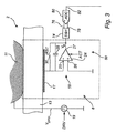
図1は、本発明の例示的実施形態による指紋感知装置2の適用例を、統合指紋感知装置2を備える携帯電話1の形態にて概略的に図示する。指紋感知装置2は、例えば、携帯電話1のロックを解除するため及び/又は携帯電話などを用いて実施されるトランザクションを承認するために用いられてもよい。本発明の種々の実施形態による指紋感知装置をこのほか、タブレット型コンピュータ、ラップトップ型コンピュータ、スマートカードをはじめとする各種の家電製品のような他の装置に使用してもよい。
FIG. 1 schematically illustrates an application example of the
図2は、図1の携帯電話1に含まれる指紋感知装置2を概略的に示す。図2に示すように、指紋感知装置2は、センサアレイ5と、電源インタフェース6と、通信インタフェース7と、を備える。センサアレイ5は、多数の感知素子8a及び8b(図面が乱雑になるのを避けるために、二つの感知素子のみに参照記号を付して示す)を備え、各感知素子は、感知素子8a及び8bに含まれる感知構造と、センサアレイ5の上面に接触する指の表面と、の間の距離を感知するように制御可能である。
FIG. 2 schematically shows a
電源インタフェース6は、ここでは接着パッドとして示される第一の接触パッド10aと第二の接触パッド10bとを備え、供給電圧Vsupplyを指紋感知装置2に接続する。
The power interface 6 includes a first contact pad 10a and a second contact pad 10b, which are shown here as adhesive pads, and connects the supply voltage V supply to the
通信インタフェース7は、指紋感知装置2の制御を可能にし、指紋感知装置2から指紋データを取得するために、多数の接着パッドを備える。
The communication interface 7 is provided with a large number of adhesive pads to enable control of the
図3は、指11をセンサアレイ5の上面に置いた状態の図2に示されるA−A’線に沿って切断される本発明の実施形態による指紋感知装置2の一部の概略断面図及び回路図である。指紋感知装置は、複数の感知素子8を備える。各感知素子は、図3に概略的に示されるように、保護誘電最上層13と、ここでは保護誘電最上層13の下の金属板17の形態の導電性感知構造17と、電荷増幅器18と、指に駆動信号VDRVを供給する駆動信号供給回路構成19と、を備える。図3に示されるように、指11の隆線が感知構造17の真上に位置づけられ、指11と感知構造17との間に誘電最上層13によって規定される最小距離が示される。
FIG. 3 is a schematic cross-sectional view of a part of the
電荷増幅器18は、感知構造17に接続される第一の入力(負の入力)25と、設置されるか別の基準電位に接続される第二の入力(正の入力)26と、出力27と、を有する演算増幅器(オペアンプ)24としてここでは概略的に図示される少なくとも一つの増幅器段を備える。さらに、電荷増幅器18は、第一の入力25と出力27との間に接続される帰還キャパシタ29と、ここではスイッチ30として機能的に図示され、帰還キャパシタ29の制御可能な放電を可能にするリセット回路構成と、を備える。電荷増幅器18は、リセット回路構成30を操作して帰還キャパシタ29を放電することによってリセットしてもよい。
The
負のフィードバック構成のオペアンプ24の場合にはよくあることであるが、第一の入力25での電圧は、第二の入力26での電圧に追従する。特定の増幅器構成に応じて、第一の入力25での電位は第二の入力26での電位と実質的に同一であるか、第一の入力25での電位と第二の入力26での電位との間に固定されたオフセットがあってもよい。図3の構成では、電荷増幅器の第一の入力25は、事実上接地されている。
As is often the case with
駆動信号供給回路構成19によって時変電位が指11に供給された場合、感知構造17と指11との間に対応する時変電位差が発生する。指11と参照構造17との間の電位差の誘発された変化は次には、電荷増幅器18の出力27に感知電圧信号Vsをもたらす。
When the time-varying potential is supplied to the finger 11 by the drive signal
アナログサンプリング回路構成74が電荷増幅器18の出力27に接続され、感知信号Vsを受け取り、サンプリングされる。サンプリング回路構成74は、サンプリング回路構成74に含まれる個々のサンプルホールド(S&H)回路を制御して、駆動信号のタイミングを参照して所望の時点で感知信号Vsをサンプリングする制御部を備えるか、同制御部に接続されてもよい。サンプリング回路構成を、以下でさらに詳細に考察する。
アナログサンプリング回路構成74は、ここでは正の出力76及び負の出力78と呼ばれ、差動アナログ・デジタル変換器(ADC)80に接続される二つの出力を備える。この差動アナログ・デジタル変換器は、正の出力76と負の出力78との間の差を、容量結合を示し、これにより、感知構造17と指11との間の距離を示しているデジタル感知信号82に変換するように構成される。
The analog
これとは別に、アナログサンプリング回路構成は、(図示しない)シングルエンドADCに接続される単一の出力を備えてもよい。この場合、サンプルはADCの前にサンプリング回路構成にて組み合わされ、結果として生じる差分信号はAD変換される。この例では、感知素子17、即ち、ピクセルのための感知回路構成は、一つのサンプルホールド回路構成モジュール74と、一つのADC80と、を備えるように図示される。しかし、ほかにも、複数のピクセルをそれぞれ一つのサンプルホールド回路構成モジュール74に接続するマルチプレクサを使用することによって、多くの異なるピクセルの間でサンプルホールド回路構成74とADC80とを共有することができる。このため、電荷増幅器18の出力27及び/又はサンプルホールド回路構成74の出力は、マルチプレクサに接続されてもよい。例えば、一つのサンプルホールド回路構成モジュール74を1列のピクセルによって共有可能である。
Separately, the analog sampling circuit configuration may include a single output connected to a single-ended ADC (not shown). In this case, the samples are combined in a sampling circuit configuration before the ADC and the resulting difference signal is AD converted. In this example, the sensing element 17, i.e., the sensing circuit configuration for the pixels, is illustrated to include one sample hold
図4は、本発明の例示的実施形態によるサンプリング回路74の概略を示す。本明細書で図示されるサンプリング回路は、八つのサンプルホールド回路40a〜40hを備える。各サンプルホールド回路は、一方の側がスイッチ44a〜44hを介して感知信号VSに接続され、他方の側がサンプリング回路74の外部の出力に接続されるキャパシタ42a〜42hを備える。この例では、サンプルホールド回路40a〜40dは第一のスイッチ48を介してADC80の正の入力76に接続され、サンプルホールド回路40e〜40hは第二のスイッチ50を介してADC80の負の入力76に接続される。さらに、キャパシタ42a〜42hそれぞれは基準電圧VREF、例えば、VDDに接続される。差動ADC80を用いるこの例では、負の入力及び正の入力の記号はADCによって規定される。サンプルホールド回路40a〜40dはADCの正の入力76に接続され、サンプルホールド回路40a〜40dによって取得されたサンプルは正のサンプルと呼ばれる。これに対応して、ADC80の負の入力に接続されるサンプルホールド回路40e〜40hによって取得されるサンプルは負のサンプルと呼ばれる。スイッチ44a〜44hは、スイッチが開である場合、対応するキャパシタ全体にわたって結果として生じる電圧が獲得されるように、実際のサンプリングを制御する。シングルエンドADCが用いられるのであれば、回路40a〜40dを正のサンプルとして単一の入力ラインに直接接続し、回路40e〜40hを折り返して、その結果、結果として生じる差分電圧がシングルエンドADCの入力に直接供給され得るように負の電圧を単一の入力ラインに供給してもよい。
FIG. 4 shows an outline of a
アナログサンプリングシーケンスの実施中、スイッチ46は、出力信号VSがサンプリング回路構成に供給されるように閉である。スイッチ48及び50は、ADC80との接続が切られるように開である。スイッチ44a〜44dは、キャパシタ充電がVSに比例するように閉である。サンプルが捕捉対象になっている場合、スイッチ44a〜44hの一つ以上は、サンプルがキャパシタに保存されるように開である。アナログサンプリングシーケンスが完了し、必要なサンプルがすべて捕捉された時点で、スイッチ46は開であり、スイッチ48及び50は閉である。次に、スイッチ44a〜44hは、キャパシタに保存されたサンプルがADC80の入力76、78に供給され、これにより、正の入力と負の入力との間の差をAD変換できるように、閉じる。
During the implementation of the analog sampling sequence, the
上記のサンプリング回路構成74は八つの個別のサンプルホールド回路40a〜40hを備えるように図示されているが、以下に図示されるように、三つ以上の任意の数のサンプルホールド回路を用いればノイズ抑制を達成することができる。
The above
サンプリング、即ち、スイッチ44a〜44hは、ほかにも駆動信号VDRVを制御する(図示しない)制御部によって制御される。これにより、サンプリングのタイミングは、駆動信号の特徴に基づいて制御され得る。さらに、アナログサンプリングシーケンスにてサンプルホールド回路40a〜40hの全部を使用する必要はない。その代わり、所望のフィルタ機能性を達成するのに必要なサンプルホールド回路のみを使用することができ、これにより、アナログサンプリングシーケンスに高度の柔軟性をもたらし、ノイズがない状態で迅速なサンプリングが可能になる。アナログサンプリングシーケンスは、連続するAD変換の間にアナログ出力信号VSがサンプリングされるシーケンスとして定義され得る。
Sampling, that is, switches 44a to 44h are also controlled by a control unit (not shown) that controls the drive signal V DRV. Thereby, the sampling timing can be controlled based on the characteristics of the drive signal. Further, it is not necessary to use all of the
図5(先行技術)は、駆動信号VDRVが複数の方形パルスを含み、駆動信号の1周期の間にアナログサンプリングが実施される場合の駆動信号VDRV及び感知信号VSを図示する。指に駆動信号VDRVが注入され、駆動パルス52が正の場合、電荷増幅器18のリセットスイッチ30が閉じられる。システムが安定すると、スイッチ30が再び開にされ、出力信号がわずかに上昇して基準レベルVREFを表す。その後、駆動信号が低下すると、指11と感知板17との間の電荷が変化することになり、出力信号VSは、指11と感知板17との間の距離に比例する値まで上昇し、信号レベルVSIGと呼ばれる。
Figure 5 (prior art), the driving signal V DRV includes a plurality of rectangular pulses, illustrating the driving signal V DRV and the sensing signal V S when the analog sampling is performed during one period of the drive signal. When the drive signal V DRV is injected into the finger and the
図5に図示される従来の相関二重サンプリングに対しては、出力信号が低のときに第一のサンプルS0が捕捉され、出力信号が高のときに第二のサンプルS1が捕捉され、結果として生じる出力信号S1〜S0は、指11と検知プレート17との間の距離をさらに正確に表すために、電荷増幅器のリセット後の任意の電圧オフセットの影響を除去する。 For the conventional correlated double sampling illustrated in FIG. 5, the first sample S 0 is captured when the output signal is low and the second sample S 1 is captured when the output signal is high. , the output signal S 1 to S 0 resulting, in order to more accurately represent the distance between the finger 11 and the detection plate 17, to remove the effects of any voltage offset after reset of the charge amplifier.
以下では、上記のアナログサンプリング回路構成74を使用するさまざまなサンプリング方式及び駆動信号を採用することによって達成されるさまざまなフィルタの機能性を参照して、本発明の種々の実施形態を考察する。
In the following, various embodiments of the present invention will be considered with reference to the functionality of the various filters achieved by adopting the various sampling schemes and drive signals using the analog
図6aは、感知信号VSが、駆動信号VDRVの周波数に対して低い周波数を有するノイズ成分を含む例を図示する。そのような低周波ノイズは、例えば、50/60Hzのノイズとして、充電器を介して装置1に導入され得る。ここで、低周波ノイズは、kHz範囲にあり得る駆動信号周波数と比較してほぼ一定であると考えられる。この図では、ノイズ成分の振幅は、ノイズの影響をいっそう明確に示すために誇張されている場合がある。
Figure 6a is a sensing signal V S is illustrates an example including a noise component having a frequency lower than the frequency of the drive signal V DRV. Such low frequency noise can be introduced into
図6に図示されるアナログサンプリングシーケンスは、スイッチ30を作動させて電荷増幅器18をリセットするリセット信号によって開始されると考えることができる。次に、第一のサンプルS0を捕捉する。サンプルS0は、ここでは重み−1を有するものとして図示されている。ここでマイナス記号は、出力信号VSが低レベルであるとき、即ち、駆動信号が高であるときにサンプルが捕捉されたことを示し、ADC80の負の入力に接続されたサンプルホールド回路40e〜40hの一つによってサンプルが捕捉されたことを示す。出力信号VSの低レベルは、基準レベルと呼ぶことができる。駆動信号の高電圧レベル及び低電圧レベルはそれぞれ、第一の電圧レベルV1及び第二の電圧レベルV2として表すことができる。
The analog sampling sequence illustrated in FIG. 6 can be considered to be initiated by a reset signal that activates the
VDRVが低になり、VSが高になると、ここでは重み+2が付与された第二のサンプルS1が捕捉され、信号レベルVSIGを表す。サンプルは、例えば、第一のサンプルS0を捕捉するサンプルホールド回路のキャパシタの2倍の容量を有するサンプルホールド回路によって捕捉されている場合、重み+2を有すると考えることができる。これとは別に、サンプリング回路構成は、図4に示されるように、全サンプリングキャパシタが同一容量であるサンプルホールド回路を備えていてもよい。その場合、サンプルには、二つ以上のサンプルホールド回路を同時に使用することによって特定の重みが付与されてもよい。ここで、サンプルの重みは、使用されるサンプルホールド回路の数に等しいと考えることができる。このため、サンプルホールド回路はアナログサンプリングシーケンス中の任意の時点でサンプルを捕捉するように任意に制御され得ることから、サンプルを規定するのは実際には、サンプルを捕捉する特定の時点であって、サンプルを捕捉するために使用される特定のサンプルホールド回路ではない。これにより、全サンプルホールド回路が等しい容量であるサンプルホールド回路構成では、サンプルの最大重みは、ADC80の入力に接続されるサンプルホールド回路の数に等しい。
V DRV is low, the V S is high, the second sample S 1 where the weight +2 is applied is captured here, represents the signal level V SIG. A sample can be considered to have a weight of +2, for example, if it is captured by a sample hold circuit that has twice the capacitance of the capacitor of the sample hold circuit that captures the first sample S 0. Apart from this, the sampling circuit configuration may include a sample hold circuit in which all sampling capacitors have the same capacitance, as shown in FIG. In that case, the sample may be given a specific weight by using two or more sample hold circuits at the same time. Here, the sample weight can be considered equal to the number of sample hold circuits used. For this reason, the sample hold circuit can be arbitrarily controlled to capture the sample at any time during the analog sampling sequence, so it is actually the specific time point at which the sample is captured that defines the sample. , Not the specific sample hold circuit used to capture the sample. Thus, in a sample hold circuit configuration where all sample hold circuits have equal capacitance, the maximum sample weight is equal to the number of sample hold circuits connected to the input of the
さらに、サンプルは、特定の時点で瞬間的に捕捉されるものとしてここでは図示される。しかし、それと同時に、各サンプルが一定の有限期間にわたる積分に対応する可能性もある。 In addition, the sample is illustrated here as being captured instantaneously at a particular point in time. However, at the same time, it is possible that each sample corresponds to an integral over a certain finite period.
最後に、VDRVが再び低レベルになり、VSが基準レベルに誘導ノイズ信号を加えたレベルに対応するレベルにあるとき、第三のサンプルS2を捕捉する。 Finally, V DRV becomes low level again, when in a level corresponding to a level V S is added inductive noise signal to a reference level to capture a third sample S 2.
サンプルの合計、S0+S1+S2は、まず負のサンプルの合計S0+S2を正のサンプルの合計(ここではS1のみ)から引いて、結果として出力信号がS1−(S0+S2)になるように、分割可能である。サンプルの合計はこのほか、2VSIG−(VREF+VREF)=VSIG−VREFとして表すことができ、結果として生じる出力はノイズの影響を受けない信号レベルと基準レベルとの間の差である。これは、結果として生じる信号であって、ADC80によってAD変換され、指紋画像を生成する際に使用される信号である。
For the sum of the samples, S 0 + S 1 + S 2 , first subtract the sum of the negative samples S 0 + S 2 from the sum of the positive samples ( only S 1 here), resulting in an output signal of S 1 − (S 0). It can be divided so that it becomes + S 2). The sum of the samples can also be expressed as 2V SIG − (V REF + V REF ) = V SIG −V REF , and the resulting output is the difference between the noise-independent signal level and the reference level. is there. This is the resulting signal, which is AD converted by the
特に、出力信号のフィルタリングの鍵は、正のサンプルの重みが負のサンプルの重みに等しいことであり、その結果、ノイズの寄与をキャンセルできる。これには、信号レベルでのサンプルと同じように、基準レベルでのサンプルにて総ノイズ寄与が等しいことが必要である。図6aに図示される例では、ノイズの勾配は一定であると考えられ、サンプル間の時間も一定であり、その結果、正のサンプルと負のサンプルとの両方に同一の総ノイズ寄与をもたらす。一般に、一定の勾配を有するノイズに対しては、代替のサンプリングの筋書きを立案することも可能であるが、サンプル間の時間を一定にすることによってフィルタリング機能性を容易に達成することができる。 In particular, the key to filtering the output signal is that the weight of the positive sample is equal to the weight of the negative sample, so that the noise contribution can be canceled. This requires that the total noise contribution be equal in the sample at the reference level, as in the sample at the signal level. In the example illustrated in FIG. 6a, the noise gradient is considered constant and the time between samples is also constant, resulting in the same total noise contribution for both positive and negative samples. .. In general, it is possible to formulate an alternative sampling scenario for noise having a constant gradient, but filtering functionality can be easily achieved by keeping the time between samples constant.
このため、駆動パルス及びアナログサンプリング回路構成を制御することによって、AD変換の前にリアルタイムでアナログフィルタリングを実施することができる。マイクロプロセッサなどの中央制御部に接続されたレジストリ内の駆動信号及びサンプリング命令の形態でアナログサンプリングシーケンスを予め定義することができる。さらに、提案されたサンプリング方式は、駆動信号及びサンプリング時間及び重みを制御することによって、さまざまなタイプのノイズを処理するためのさまざまなタイプのアナログフィルタの形成に高度な柔軟性をもたらす。 Therefore, by controlling the drive pulse and the analog sampling circuit configuration, analog filtering can be performed in real time before the AD conversion. An analog sampling sequence can be predefined in the form of drive signals and sampling instructions in a registry connected to a central control unit such as a microprocessor. In addition, the proposed sampling scheme provides a high degree of flexibility in the formation of different types of analog filters for handling different types of noise by controlling the drive signal and sampling time and weights.
アナログサンプリングシーケンスの後に、アナログ・デジタル変換シーケンスが続き、このとき、感知アレイ内の感知素子からのピクセル値が、接続された読み出し回路構成によって読み取られて、指紋画像を形成する。 The analog sampling sequence is followed by an analog-to-digital conversion sequence, where pixel values from the sensing elements in the sensing array are read by the connected readout circuit configuration to form a fingerprint image.
また、上記のアナログフィルタリングを使用すると、隣接するサンプル間の時間は、各サンプルがその後のデジタルフィルタリングに使用するために個別にAD変換されることになっていた場合に達成可能な時間よりも短くなり得る。 Also, using the analog filtering described above, the time between adjacent samples is shorter than the time achievable if each sample were to be AD converted individually for subsequent digital filtering. Can be.
さらに、上記のサンプリングは、二次フィルタについての記載である。上記の原理を遵守しながら、サンプルの数を増やすことによって、さらに鮮明な周波数応答を提供する高次フィルタが形成されることが容易にわかる。このほかのフィルタの例を以下に記載する。 Further, the above sampling is a description of a quadratic filter. It is easy to see that by increasing the number of samples while adhering to the above principles, higher order filters that provide a sharper frequency response are formed. Examples of other filters are described below.
高次フィルタの一例を図6bに図示する。ここでは、三つのサンプルが基準レベルS0、S2及びS4にて捕捉され、二つのサンプルが信号レベルS1及びS3にて捕捉される。サンプルS1及びS3は重み+2を有し、サンプルS2は重み−2を有する。ここではこのほか、サンプル間の時間が一定である。サンプルを組み合わせた後に結果として生じる信号は、(S1+S3)−(S0+S2+S4)=(2+2)VSIG−(1+2+1)VREF=4VSIG−4VREFとなる。ここでは、VSIGとVREFとの間の差に4を掛ける。このことは、読み出しシステム全体がサンプリング方式を考慮に入れることにより、結果として得られるデジタル信号がVSIG−VREFの倍数を表すかどうかを理解するため、結果として得られるAD変換後のものにて説明されることになる。 An example of a higher-order filter is shown in FIG. 6b. Here, three samples are captured at reference levels S 0 , S 2 and S 4 , and two samples are captured at signal levels S 1 and S 3. Samples S 1 and S 3 have a weight of +2 and sample S 2 has a weight of -2. In addition to this, the time between samples is constant here. The resulting signal after combining the samples is (S 1 + S 3 ) − (S 0 + S 2 + S 4 ) = (2 + 2) V SIG − (1 + 2 + 1) V REF = 4V SIG -4V REF . Here, the difference between V SIG and V REF is multiplied by 4. This is due to the resulting AD conversion to understand whether the resulting digital signal represents a multiple of V SIG − V REF by taking the sampling scheme into account throughout the readout system. Will be explained.
図6cは、高周波方形パルスの形態のノイズが感知信号に存在する例を図示する。高周波方形ノイズは、例えばスイッチト電源から、又は高周波数で動作するディスプレイ又はタッチスクリーンのような装置内の他の構成要素からのスイッチングノイズとして導入することができる。 FIG. 6c illustrates an example in which noise in the form of a high frequency square pulse is present in the sensing signal. High frequency square noise can be introduced, for example, from switched power supplies or as switching noise from other components within the device, such as displays or touch screens operating at high frequencies.
図6cでは、出力信号VSがノイズ信号の影響を受ける場合にサンプルS1及びS2が捕捉され、出力信号VSがノイズ信号の影響を受けない場合にサンプルS0及びS3が捕捉される。 In Figure 6c, the sample S 1 and S 2 are captured when the output signal V S is affected by the noise signal, the sample S 0 and S 3 are captured when the output signal V S is not affected by the noise signal To.
方形ノイズの場合、あるいはノイズレベルが急激に変化する類似のタイプのノイズに対してはこのほか、VSがノイズの影響を受ける場合に補足されるサンプルが、VSがノイズの影響を受けない場合のサンプルの重みに等しいことが必要である。 For square noise, or noise level Other for rapidly changing similar type of noise, the sample V S is supplemented to be affected by noise, V S is not affected by noise It should be equal to the weight of the sample in the case.
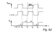
図6dは、駆動信号が二つの連続する駆動パルスの間の半周期だけ位相シフトされるか、遅延される状況を示す。ノイズが駆動信号と類似するか等しい特性を有する場合、ノイズが無効になるように出力信号をサンプリングすることが困難であるか、不可能である場合がある。ノイズが駆動信号とほぼ同じ周波数であることが観察された場合、駆動信号は、第二のパルスが第一のパルスに対して半周期だけ位相シフト、即ち、遅延される二つの連続するパルスとして形成可能であり、これにより、サンプルS0〜S4で図示されるように上記と同一の方法でノイズ除去が可能となる。このため、駆動パルスのデューティサイクルは、さまざまな種類のノイズに対するノイズ抑制を容易にするように変更することができる。さらに、駆動信号は、パルスの形状及び連続パルス間の時間を任意に選択することができる場合には、一連の個々のパルスを含むことがある。そのような実施形態では、駆動信号周波数、周期及びデューティサイクルの概念は適用できないことがある。 FIG. 6d shows a situation in which the drive signal is phase-shifted or delayed by half a cycle between two consecutive drive pulses. If the noise has similar or equal characteristics to the drive signal, it may be difficult or impossible to sample the output signal so that the noise is nullified. When it is observed that the noise is about the same frequency as the drive signal, the drive signal is as two consecutive pulses in which the second pulse is phase-shifted by half a period with respect to the first pulse, ie delayed. It can be formed, which enables noise removal in the same manner as described above, as illustrated in Samples S 0- S 4. Therefore, the duty cycle of the drive pulse can be changed to facilitate noise suppression for various types of noise. In addition, the drive signal may include a series of individual pulses where the shape of the pulses and the time between continuous pulses can be arbitrarily selected. In such embodiments, the concepts of drive signal frequency, period and duty cycle may not be applicable.
図7a〜図7cは、方形波の形態の駆動信号と同一であるか類似する周波数を有する高周波ノイズを処理するために駆動信号をどのように適合させることができるかの他の例を概略的に図示する。図7aでは、ノイズは、駆動信号と同一の周波数を有し、ほかにも駆動信号と同相である。これは上記の方法によるフィルタリングが不可能であることを意味する。特に、図7aに図示される状況では、VSの信号レベルへのノイズ寄与がVSの基準レベルへのノイズ寄与に等しいサンプルを取得することは不可能である。 7a-7c schematically show other examples of how the drive signal can be adapted to handle high frequency noise with frequencies that are the same as or similar to the drive signal in the form of a square wave. Illustrated in. In FIG. 7a, the noise has the same frequency as the drive signal and is also in phase with the drive signal. This means that filtering by the above method is not possible. In particular, in the situation shown in Figure 7a, it is not possible noise contribution to the signal level of V S to obtain a sample equal to the noise contribution to the reference level V S.
図7bでは、駆動信号は、駆動信号の高レベルと低レベルとのあらゆる組み合わせに対してノイズ寄与の高レベル及び低レベルにてサンプルを取得することができるため、ノイズの2倍の周波数を有することにより、ノイズのフィルタリングを可能にする。このため、駆動信号の周波数を増加又は減少させて変更することによって、図示されたノイズのフィルタリングが可能になる。図7aに図示される駆動信号の周波数は、例えば整数で乗算又は除算することができる。 In FIG. 7b, the drive signal has twice the frequency of noise because samples can be taken at high and low levels of noise contribution for any combination of high and low levels of the drive signal. This allows for noise filtering. Therefore, by increasing or decreasing the frequency of the drive signal and changing it, the illustrated noise can be filtered. The frequency of the drive signal illustrated in FIG. 7a can be multiplied or divided by, for example, an integer.
図7cは、駆動信号が図7aの駆動信号に対して位相シフトされた例を図示する。またここでは、フィルタを構成するためにサンプリングすることも可能である。ノイズ周波数が駆動信号周波数と一致することがわかっているか疑われている場合、駆動信号は、例えば、周期の1/4だけ位相シフトされるか、観察されたノイズが最小になるまで少しずつ位相シフトされ得る。これにより、フィルタはさまざまな種類のノイズを抑制することを習得することができる。このため、例えば、特定の充電器が使用されるか、特定の種類のノイズを発生させることが知られている装置の一定の特徴が使用されている場合に、さまざまなノイズ条件に対して特定のサンプリングプロファイルを記憶することも可能である。 FIG. 7c illustrates an example in which the drive signal is phase-shifted with respect to the drive signal of FIG. 7a. It is also possible here to sample to configure the filter. If it is known or suspected that the noise frequency matches the drive signal frequency, the drive signal will be phase-shifted, for example, by a quarter of the period, or gradually phased until the observed noise is minimized. Can be shifted. This allows the filter to learn to suppress different types of noise. Thus, for example, when a particular charger is used or certain features of a device known to generate a particular type of noise are used, it is specific for different noise conditions. It is also possible to store the sampling profile of.
さらに、駆動信号にはこのほか、パルス列が含まれることがある。このパルス列では、個々のパルスが異なり、即ち、異なるパルス長を有し、これにより駆動信号の周波数とノイズの周波数とが一致するという筋書きが回避される。 Further, the drive signal may also include a pulse train. In this pulse train, the scenario that the individual pulses are different, that is, they have different pulse lengths, so that the frequency of the drive signal and the frequency of the noise match is avoided.
図8aは、駆動信号が正弦波を含み、ノイズが駆動信号に対してほぼ一定である例を図示する。正弦波は実際には同じ効果を得るためにsincパルスで置き換えることができる。 FIG. 8a illustrates an example in which the drive signal includes a sine wave and the noise is substantially constant with respect to the drive signal. The sine wave can actually be replaced with a sinc pulse to get the same effect.
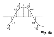
図8bは、サンプリングキャパシタの係数が駆動信号(ここでは正弦波)の形状、即ち、振幅と整列するように構成された例を図示する。サンプリング係数を駆動信号の振幅に適応させ、駆動信号の1周期中に複数のサンプルを捕捉することにより、高周波数選択性を有するフィルタを実現することができる。異なる係数は、上記の方法のいずれか、例えば、所望の係数をもたらす各サンプルのための多数のキャパシタを組み合わせることによって、あるいはさまざまなサイズのキャパシタを使用することによって、達成され得る。 FIG. 8b illustrates an example in which the coefficients of the sampling capacitor are configured to align with the shape of the drive signal (here, a sine wave), that is, the amplitude. A filter having high frequency selectivity can be realized by adapting the sampling coefficient to the amplitude of the drive signal and capturing a plurality of samples in one cycle of the drive signal. Different coefficients can be achieved by any of the above methods, eg, by combining a large number of capacitors for each sample that yield the desired coefficients, or by using capacitors of different sizes.
サンプルが正弦波の最大振幅及び最小振幅それぞれで捕捉される必要はない。しかし、フィルタリングが適切に機能するためには、駆動信号が同一の相対電圧レベルV1にある場合に負と呼ばれる全サンプルが捕捉され、駆動信号のV1とは異なる同一の相対電圧レベルV2で正と呼ばれる全サンプルが捕捉されることが必要である。 The sample need not be captured at the maximum and minimum amplitudes of the sine wave, respectively. However, for filtering to work properly, all samples called negative are captured when the drive signal is at the same relative voltage level V 1 , and the same relative voltage level V 2 different from the drive signal V 1 is captured. It is necessary that all samples called positive in are captured.
図9は、これまでに考察したノイズ低減のための方法の一般的な方法ステップを概説するフローチャートである。この方法は、駆動信号を提供するステップ902、少なくとも三つのサンプルを捕捉するステップ904、信号のノイズが抑制されるようにサンプルの合計を形成するステップ906、及びデジタル信号を形成するステップ908を含む。
FIG. 9 is a flow chart outlining the general method steps of the methods for noise reduction discussed so far. The method includes
この方法の特徴は、指紋感知装置での信号のサンプリングに関してこれまでに考察したものと類似している。以上の説明から理解できるように、記載された方法論を使用して、無数の異なるフィルタを形成することができる。ここで、フィルタ機能性を可能にする重要な特徴の鍵は、リアルタイムアナログサンプリング及び駆動信号の同時制御である。 The characteristics of this method are similar to those discussed so far regarding signal sampling in fingerprint detectors. As can be seen from the above description, the described methodologies can be used to form a myriad of different filters. Here, the key to the important features that enable the filter functionality is real-time analog sampling and simultaneous control of the drive signal.
上記の例から理解できるように、さまざまなタイプのノイズを抑制するために駆動信号を調整するのには多くの異なる方法がある。ノイズ特性が完全に未知である場合、多数の予め設定されたアナログサンプリングシーケンスを採用し、得られたフィルタリング済みの信号を評価して、サンプリングシーケンスのうちのいずれのシーケンスがノイズ成分の最も低い出力信号を生成するかを判定することが可能である。これにより、ノイズ特性が未知であってもノイズを抑圧することができる。ノイズ特性が未知である場合、自己学習アルゴリズムを用いて、読み出し回路構成からのフィードバックに基づいてサンプリングが適応される適応フィルタを形成してもよい。 As can be seen from the above example, there are many different ways to tune the drive signal to suppress different types of noise. If the noise characteristics are completely unknown, a number of preset analog sampling sequences are used to evaluate the resulting filtered signal, and any of the sampling sequences is the output with the lowest noise content. It is possible to determine whether to generate a signal. As a result, noise can be suppressed even if the noise characteristics are unknown. If the noise characteristics are unknown, a self-learning algorithm may be used to form an adaptive filter to which sampling is applied based on feedback from the readout circuit configuration.
多くの場合、ノイズの特性のいくつかがわかっているため、特定のノイズを抑えるためにアナログサンプリングシーケンスを予め設定することができる。既知の特性を有するノイズは、例えば、既知のスイッチング周波数を有する装置充電器から、あるいはディスプレイ又はタッチスクリーンなどの装置内の他の構成要素から発生することがある。 In many cases, some of the noise characteristics are known, so analog sampling sequences can be preset to suppress specific noise. Noise with known characteristics can occur, for example, from device chargers with known switching frequencies, or from other components within the device, such as displays or touch screens.
装置内のノイズ特性を判定し、判定されたノイズを抑制するようにアナログサンプリングシーケンスを構成することも可能である。 It is also possible to determine the noise characteristics in the device and configure the analog sampling sequence to suppress the determined noise.
本発明を、その特定の例示的な実施形態を参照して説明してきたが、当業者にとっては多くの異なる変更、修正などが明らかになるであろう。また、感知装置が本発明の機能性を実行することができるのであれば、感知装置の一部をさまざまな方法で省略、交換、又は配置してもよいことに留意されたい。 Although the present invention has been described with reference to its particular exemplary embodiment, many different changes, modifications, etc. will be apparent to those skilled in the art. It should also be noted that parts of the sensing device may be omitted, replaced, or arranged in various ways as long as the sensing device is capable of performing the functionality of the present invention.
さらに、開示された実施形態に対する変形は、図面、開示、及び添付の特許請求の範囲の検討から、請求された発明を実施する際の当業者によって理解され、達成され得る。請求の範囲では、「備える」という文言は他の要素又は工程を除外するものではなく、不定冠詞「a」又は「an」は複数を除外するものではない。単に特定の手段が相互に異なる従属項に記載されているというだけでは、このような手段の組み合わせを有利に用いることができないことを示すことにはならない。 Further, modifications to the disclosed embodiments can be understood and achieved by one of ordinary skill in the art in carrying out the claimed invention from the drawings, disclosures, and examination of the appended claims. In the claims, the word "prepare" does not exclude other elements or steps, and the indefinite articles "a" or "an" do not exclude more than one. The mere fact that specific means are described in different dependent terms does not indicate that such a combination of means cannot be used in an advantageous manner.
Claims (22)
前記容量性指紋感知装置は複数の感知素子を備え、各感知素子は
前記指による接触対象である保護誘電最上層と、
前記最上層の下に配置される導電性感知構造と、
前記指と前記感知構造との間の距離を示すアナログ感知信号を提供する感知回路構成
と、
を備え、
前記指紋感知装置はさらに、
前記指と前記感知構造との間の電位差に変化をもたらす最大電圧レベル及び最小電圧レベルを有する少なくとも一つの駆動パルスを含む駆動信号を提供するように構成される駆動信号回路構成と、
前記感知信号をサンプリングするために配置される少なくとも三つのアナログサンプルホールド回路と、前記少なくとも三つのアナログサンプルホールド回路を個別に制御して、特定の時間にサンプルを捕捉し、これにより、少なくとも三つのサンプルを形成するサンプリング制御部と、を備えるアナログサンプリング回路構成であって、前記少なくとも三つのサンプルは、前記駆動信号が第一の電圧レベルV1にあるときに捕捉される少なくとも一つのサンプルと、前記駆動信号がV1とは異なる第二の電圧レベルV2にあるときに捕捉される少なくとも一つのサンプルと、を含む、アナログサンプリング回路構成と、
前記アナログサンプリング回路構成に接続され、前記少なくとも三つのサンプルの組み合わせを前記感知構造と前記指との間の容量結合を示すデジタル感知信号に変換するように構成されるアナログ・デジタル変換器(ADC)であって、前記少なくとも三つのサンプルは、前記特定の時間に、ノイズ成分が抑制されるように、前記組み合わせが形成された場合に前記感知信号から捕捉される、アナログ・デジタル変換器と、
を備える、容量性指紋感知装置。 A capacitive fingerprint detector that detects the fingerprint pattern of a finger.
The capacitive fingerprint sensing device includes a plurality of sensing elements, and each sensing element has a protective dielectric uppermost layer to be contacted by the finger.
The conductive sensing structure arranged under the uppermost layer and
A sensing circuit configuration that provides an analog sensing signal indicating the distance between the finger and the sensing structure.
With
The fingerprint detector further
A drive signal circuit configuration configured to provide a drive signal including at least one drive pulse having a maximum voltage level and a minimum voltage level that causes a change in the potential difference between the finger and the sensing structure.
At least three analog sample hold circuits arranged to sample the sensed signal and at least three analog sample hold circuits are individually controlled to capture samples at specific times, thereby at least three. An analog sampling circuit configuration including a sampling control unit for forming a sample, wherein the at least three samples include at least one sample captured when the drive signal is at the first voltage level V1 and said. An analog sampling circuit configuration, including at least one sample captured when the drive signal is at a second voltage level V2 different from V1.
An analog-to-digital converter (ADC) connected to the analog sampling circuit configuration and configured to convert a combination of the at least three samples into a digital sensing signal indicating a capacitive coupling between the sensing structure and the finger. The at least three samples are an analog-to-digital converter that is captured from the sensing signal when the combination is formed so that the noise component is suppressed at the particular time.
A capacitive fingerprint detector.
電位差の前記変化を提供する最大電圧レベル及び最小電圧レベルを有する少なくとも一つの駆動パルスを含む駆動信号を提供するステップと、
前記感知信号の少なくとも三つのサンプルを捕捉するステップであって、前記少なくとも三つのサンプルは、前記駆動信号が第一の電圧レベルV1にあるときに捕捉された少なくとも一つのサンプルと、前記駆動信号がV1とは異なる第二の電圧レベルV2にあるときに捕捉された少なくとも一つのサンプルと、を含む、ステップと、
前記少なくとも三つのサンプルの合計を形成するステップであって、前記サンプルは、前記合計が形成されたときに、ノイズ成分が抑制されるように適切な時間に前記感知信号から選択される、ステップと、
前記少なくとも三つのサンプルの前記合計からデジタル信号を形成するステップと、
を備える方法。 A method of reducing noise in a capacitive fingerprint sensing device including a plurality of sensing elements, wherein the fingerprint sensing device provides a sensing circuit that provides an analog sensing signal indicating a distance between a finger and a sensing structure of the sensing element. In a method comprising a configuration and a drive signal circuit configuration that provides a change in potential difference between the finger and the sensing structure, the method.
A step of providing a drive signal comprising at least one drive pulse having a maximum voltage level and a minimum voltage level that provides said change in potential difference.
In the step of capturing at least three samples of the sensed signal, the at least three samples include at least one sample captured when the drive signal is at the first voltage level V1 and the drive signal. Steps, including at least one sample captured when at a second voltage level V2, which is different from V1.
A step of forming the sum of at least three samples, wherein the sample is selected from the sensed signals at an appropriate time so that the noise component is suppressed when the sum is formed. ,
The step of forming a digital signal from the sum of the at least three samples,
How to prepare.
Applications Claiming Priority (3)
| Application Number | Priority Date | Filing Date | Title |
|---|---|---|---|
| SE1551553 | 2015-11-30 | ||
| SE1551553-9 | 2015-11-30 | ||
| PCT/SE2016/051160 WO2017095304A1 (en) | 2015-11-30 | 2016-11-23 | Analog sampling system and method for noise suppression in a capacitive fingerprint sensing device. |
Publications (2)
| Publication Number | Publication Date |
|---|---|
| JP2019507402A JP2019507402A (en) | 2019-03-14 |
| JP6871923B2 true JP6871923B2 (en) | 2021-05-19 |
Family
ID=58337117
Family Applications (1)
| Application Number | Title | Priority Date | Filing Date |
|---|---|---|---|
| JP2018525708A Active JP6871923B2 (en) | 2015-11-30 | 2016-11-23 | Analog sampling systems and methods for noise suppression in capacitive fingerprint detectors |
Country Status (7)
| Country | Link |
|---|---|
| US (1) | US9600707B1 (en) |
| EP (1) | EP3384426B1 (en) |
| JP (1) | JP6871923B2 (en) |
| KR (1) | KR20180088804A (en) |
| CN (1) | CN107251047B (en) |
| TW (1) | TWI611330B (en) |
| WO (1) | WO2017095304A1 (en) |
Families Citing this family (17)
| Publication number | Priority date | Publication date | Assignee | Title |
|---|---|---|---|---|
| US8485442B2 (en) | 2009-07-02 | 2013-07-16 | Biometric Payment Solutions | Electronic transaction verification system with biometric authentication |
| TWI727040B (en) * | 2016-05-13 | 2021-05-11 | 瑞典商指紋卡公司 | Fingerprint sensing device and method therein for noise detection |
| TWI719203B (en) | 2016-05-13 | 2021-02-21 | 瑞典商指紋卡公司 | Fingerprint sensing device and method therein for noise detection |
| US9864895B1 (en) * | 2016-07-07 | 2018-01-09 | Fingerprint Cards Ab | Fingerprint sensing system with finger detect |
| CN106845422B (en) * | 2017-01-22 | 2020-12-22 | Oppo广东移动通信有限公司 | Fingerprint identification module, fingerprint identification method and mobile terminal |
| SE1750159A1 (en) * | 2017-02-17 | 2018-08-18 | Fingerprint Cards Ab | Canceling out impairment data in fingerprint images |
| US10346665B2 (en) * | 2017-05-30 | 2019-07-09 | Sunasic Technologies Limited | Noise reduced capacitive image sensor and method operating the same |
| CN107980141B (en) | 2017-10-18 | 2021-12-17 | 深圳市汇顶科技股份有限公司 | Fingerprint sensor and terminal equipment |
| US20190179446A1 (en) * | 2017-12-13 | 2019-06-13 | Cypress Semiconductor Corporation | Hover sensing with multi-phase self-capacitance method |
| KR102410015B1 (en) * | 2017-12-27 | 2022-06-16 | 삼성전자주식회사 | Touch screen controller, Touch screen system having the same and Operating method of touch screen controller |
| CN111801682A (en) * | 2018-03-14 | 2020-10-20 | 指纹卡有限公司 | Method for filtering fingerprint pattern signal and fingerprint sensing device |
| TWI687869B (en) * | 2018-12-19 | 2020-03-11 | 大陸商北京集創北方科技股份有限公司 | Method for removing fingerprint sensing noise of glass cover plate, fingerprint recognition device for glass cover plate and information processing device |
| US20200233558A1 (en) * | 2019-01-22 | 2020-07-23 | Novatek Microelectronics Corp. | Fingerprint and touch sensor and related signal processing method |
| CN111353421A (en) * | 2019-04-19 | 2020-06-30 | 神盾股份有限公司 | Optical fingerprint sensing device |
| KR20210066976A (en) | 2019-11-28 | 2021-06-08 | 삼성디스플레이 주식회사 | Display device having fingerprint sensing function and operating method thereof |
| TWI727547B (en) * | 2019-12-12 | 2021-05-11 | 國立臺灣大學 | Noise Suppressor |
| CN113448458A (en) * | 2020-03-25 | 2021-09-28 | 昇佳电子股份有限公司 | Capacitance sensing circuit |
Family Cites Families (28)
| Publication number | Priority date | Publication date | Assignee | Title |
|---|---|---|---|---|
| TW528989B (en) * | 2001-05-22 | 2003-04-21 | Nitgen Co Ltd | Method and apparatus for discriminating latent fingerprint in optical fingerprint input apparatus |
| US6941004B2 (en) * | 2001-12-06 | 2005-09-06 | Motorola, Inc. | Method and apparatus for asperity sensing and storage |
| TWI236636B (en) * | 2003-05-20 | 2005-07-21 | Lightuning Tech Inc | Sweep-type fingerprint sensor module and a sensing method therefor |
| US8358815B2 (en) * | 2004-04-16 | 2013-01-22 | Validity Sensors, Inc. | Method and apparatus for two-dimensional finger motion tracking and control |
| US8447077B2 (en) * | 2006-09-11 | 2013-05-21 | Validity Sensors, Inc. | Method and apparatus for fingerprint motion tracking using an in-line array |
| US7864992B2 (en) * | 2004-06-18 | 2011-01-04 | Fingerprint Cards Ab | Fingerprint sensor element |
| US7113116B2 (en) * | 2005-01-26 | 2006-09-26 | Analog Devices, Inc. | Sample and hold apparatus |
| US8471570B2 (en) * | 2008-01-15 | 2013-06-25 | Pixcir Microelectronics Co., Ltd. | Device for quantifying an electric unbalance and touch detection system incorporating it |
| US8116540B2 (en) * | 2008-04-04 | 2012-02-14 | Validity Sensors, Inc. | Apparatus and method for reducing noise in fingerprint sensing circuits |
| TWI363290B (en) * | 2008-10-29 | 2012-05-01 | Myson Century Inc | Signal conversion control circuit for touch screen and method thereof |
| WO2012048263A1 (en) | 2010-10-08 | 2012-04-12 | Authentec, Inc. | Finger sensing device including differential measurement circuitry and related methods |
| US9086439B2 (en) * | 2011-02-25 | 2015-07-21 | Maxim Integrated Products, Inc. | Circuits, devices and methods having pipelined capacitance sensing |
| KR101304195B1 (en) * | 2011-06-24 | 2013-09-05 | 주식회사 하이딥 | Capacitance sensor with improved noise filtering chracteristics, method and computer-readable recording medium for noise filtering of capacitance sensor |
| CH705869A1 (en) | 2011-12-02 | 2013-06-14 | Advanced Silicon S A | Interface and capacitive sensor reading method. |
| US9740343B2 (en) * | 2012-04-13 | 2017-08-22 | Apple Inc. | Capacitive sensing array modulation |
| US9372582B2 (en) * | 2012-04-19 | 2016-06-21 | Atmel Corporation | Self-capacitance measurement |
| US9390307B2 (en) * | 2012-05-04 | 2016-07-12 | Apple Inc. | Finger biometric sensing device including error compensation circuitry and related methods |
| EP2853906A4 (en) * | 2012-05-22 | 2016-10-12 | Silicon Display Technology | Capacitive fingerprint sensor |
| CN202677425U (en) * | 2012-07-12 | 2013-01-16 | 邓国强 | Capacitive type sensing device and optical fingerprint gatherer |
| US9035895B2 (en) * | 2012-07-13 | 2015-05-19 | Apple Inc. | Redundant sensing element sampling |
| WO2014099514A1 (en) * | 2012-12-18 | 2014-06-26 | Apple Inc. | Electronic device including device ground coupled finger coupling electrode and array shielding electrode and related methods |
| JP6074741B2 (en) * | 2013-02-26 | 2017-02-08 | コニカミノルタ株式会社 | Optical writing apparatus and image forming apparatus |
| CN107273790A (en) * | 2013-07-09 | 2017-10-20 | 指纹卡有限公司 | Fingerprint sensing system and method |
| US9576176B2 (en) * | 2013-07-22 | 2017-02-21 | Apple Inc. | Noise compensation in a biometric sensing device |
| JP6224438B2 (en) | 2013-11-26 | 2017-11-01 | ルネサスエレクトロニクス株式会社 | Semiconductor device |
| US9152841B1 (en) * | 2014-03-24 | 2015-10-06 | Fingerprint Cards Ab | Capacitive fingerprint sensor with improved sensing element |
| TWI503757B (en) * | 2014-05-30 | 2015-10-11 | Image Match Desgin Inc | Fingerprint sensor |
| US10354113B2 (en) * | 2014-10-16 | 2019-07-16 | Crucialtec Co., Ltd. | Fingerprint detecting apparatus canceling offset and control method thereof |
-
2016
- 2016-06-29 US US15/196,617 patent/US9600707B1/en active Active
- 2016-09-12 TW TW105129582A patent/TWI611330B/en active
- 2016-11-23 JP JP2018525708A patent/JP6871923B2/en active Active
- 2016-11-23 WO PCT/SE2016/051160 patent/WO2017095304A1/en active Application Filing
- 2016-11-23 CN CN201680006248.6A patent/CN107251047B/en active Active
- 2016-11-23 KR KR1020187013606A patent/KR20180088804A/en not_active Application Discontinuation
- 2016-11-23 EP EP16871148.9A patent/EP3384426B1/en active Active
Also Published As
| Publication number | Publication date |
|---|---|
| EP3384426A1 (en) | 2018-10-10 |
| TWI611330B (en) | 2018-01-11 |
| JP2019507402A (en) | 2019-03-14 |
| US9600707B1 (en) | 2017-03-21 |
| CN107251047A (en) | 2017-10-13 |
| WO2017095304A1 (en) | 2017-06-08 |
| EP3384426B1 (en) | 2023-03-29 |
| TW201721391A (en) | 2017-06-16 |
| EP3384426A4 (en) | 2019-06-19 |
| CN107251047B (en) | 2019-06-04 |
| KR20180088804A (en) | 2018-08-07 |
Similar Documents
| Publication | Publication Date | Title |
|---|---|---|
| JP6871923B2 (en) | Analog sampling systems and methods for noise suppression in capacitive fingerprint detectors | |
| US9460576B2 (en) | Capacitive fingerprint sensing device with demodulation circuitry in sensing element | |
| US9449212B2 (en) | Capacitive fingerprint sensor with sensing elements comprising timing circuitry | |
| US9448267B2 (en) | Noise measurement in capacitive touch sensors | |
| EP3455791B1 (en) | Fingerprint sensing device and method therein for noise detection | |
| KR101511418B1 (en) | Phase compensation for multi-stimulus controller | |
| US10831321B2 (en) | Parallel sensing touch control device and operating method thereof | |
| KR20150123488A (en) | Touch sensing device | |
| WO2017184057A1 (en) | Fingerprint sensing system with adaptive power control | |
| US9923572B2 (en) | Delta modulator receive channel for capacitance measurement circuits | |
| KR20150056685A (en) | Signal Processing Circuit for Touch Screen and Control Method there-of | |
| CN112363003B (en) | Self-capacitance detection circuit, touch chip and electronic equipment |
Legal Events
| Date | Code | Title | Description |
|---|---|---|---|
| A621 | Written request for application examination |
Free format text: JAPANESE INTERMEDIATE CODE: A621 Effective date: 20191017 |
|
| A977 | Report on retrieval |
Free format text: JAPANESE INTERMEDIATE CODE: A971007 Effective date: 20201109 |
|
| A131 | Notification of reasons for refusal |
Free format text: JAPANESE INTERMEDIATE CODE: A131 Effective date: 20201208 |
|
| A521 | Request for written amendment filed |
Free format text: JAPANESE INTERMEDIATE CODE: A523 Effective date: 20210303 |
|
| TRDD | Decision of grant or rejection written | ||
| A01 | Written decision to grant a patent or to grant a registration (utility model) |
Free format text: JAPANESE INTERMEDIATE CODE: A01 Effective date: 20210406 |
|
| A61 | First payment of annual fees (during grant procedure) |
Free format text: JAPANESE INTERMEDIATE CODE: A61 Effective date: 20210416 |
|
| R150 | Certificate of patent or registration of utility model |
Ref document number: 6871923 Country of ref document: JP Free format text: JAPANESE INTERMEDIATE CODE: R150 |
|
| S111 | Request for change of ownership or part of ownership |
Free format text: JAPANESE INTERMEDIATE CODE: R313113 |
|
| S531 | Written request for registration of change of domicile |
Free format text: JAPANESE INTERMEDIATE CODE: R313531 |
|
| R350 | Written notification of registration of transfer |
Free format text: JAPANESE INTERMEDIATE CODE: R350 |