JP6863707B2 - Display driver, display device and display panel - Google Patents
Display driver, display device and display panel Download PDFInfo
- Publication number
- JP6863707B2 JP6863707B2 JP2016202870A JP2016202870A JP6863707B2 JP 6863707 B2 JP6863707 B2 JP 6863707B2 JP 2016202870 A JP2016202870 A JP 2016202870A JP 2016202870 A JP2016202870 A JP 2016202870A JP 6863707 B2 JP6863707 B2 JP 6863707B2
- Authority
- JP
- Japan
- Prior art keywords
- source
- capacitance
- circuit
- display panel
- driver
- Prior art date
- Legal status (The legal status is an assumption and is not a legal conclusion. Google has not performed a legal analysis and makes no representation as to the accuracy of the status listed.)
- Active
Links
- 238000001514 detection method Methods 0.000 claims description 187
- 238000000034 method Methods 0.000 claims description 34
- 230000005540 biological transmission Effects 0.000 claims description 18
- 239000004020 conductor Substances 0.000 claims description 8
- 239000004065 semiconductor Substances 0.000 claims description 8
- 239000000758 substrate Substances 0.000 description 16
- 239000004973 liquid crystal related substance Substances 0.000 description 10
- 239000011159 matrix material Substances 0.000 description 8
- 239000011521 glass Substances 0.000 description 4
- 238000010586 diagram Methods 0.000 description 3
- 239000010409 thin film Substances 0.000 description 3
- 239000003086 colorant Substances 0.000 description 2
- 238000013459 approach Methods 0.000 description 1
- 238000012986 modification Methods 0.000 description 1
- 230000004048 modification Effects 0.000 description 1
Images


Classifications
-
- G—PHYSICS
- G06—COMPUTING; CALCULATING OR COUNTING
- G06F—ELECTRIC DIGITAL DATA PROCESSING
- G06F3/00—Input arrangements for transferring data to be processed into a form capable of being handled by the computer; Output arrangements for transferring data from processing unit to output unit, e.g. interface arrangements
- G06F3/01—Input arrangements or combined input and output arrangements for interaction between user and computer
- G06F3/03—Arrangements for converting the position or the displacement of a member into a coded form
- G06F3/041—Digitisers, e.g. for touch screens or touch pads, characterised by the transducing means
- G06F3/0412—Digitisers structurally integrated in a display
-
- G—PHYSICS
- G06—COMPUTING; CALCULATING OR COUNTING
- G06F—ELECTRIC DIGITAL DATA PROCESSING
- G06F3/00—Input arrangements for transferring data to be processed into a form capable of being handled by the computer; Output arrangements for transferring data from processing unit to output unit, e.g. interface arrangements
- G06F3/01—Input arrangements or combined input and output arrangements for interaction between user and computer
- G06F3/03—Arrangements for converting the position or the displacement of a member into a coded form
- G06F3/041—Digitisers, e.g. for touch screens or touch pads, characterised by the transducing means
- G06F3/0416—Control or interface arrangements specially adapted for digitisers
- G06F3/04164—Connections between sensors and controllers, e.g. routing lines between electrodes and connection pads
-
- G—PHYSICS
- G06—COMPUTING; CALCULATING OR COUNTING
- G06F—ELECTRIC DIGITAL DATA PROCESSING
- G06F3/00—Input arrangements for transferring data to be processed into a form capable of being handled by the computer; Output arrangements for transferring data from processing unit to output unit, e.g. interface arrangements
- G06F3/01—Input arrangements or combined input and output arrangements for interaction between user and computer
- G06F3/03—Arrangements for converting the position or the displacement of a member into a coded form
- G06F3/041—Digitisers, e.g. for touch screens or touch pads, characterised by the transducing means
- G06F3/0416—Control or interface arrangements specially adapted for digitisers
- G06F3/04166—Details of scanning methods, e.g. sampling time, grouping of sub areas or time sharing with display driving
- G06F3/041662—Details of scanning methods, e.g. sampling time, grouping of sub areas or time sharing with display driving using alternate mutual and self-capacitive scanning
-
- G—PHYSICS
- G06—COMPUTING; CALCULATING OR COUNTING
- G06F—ELECTRIC DIGITAL DATA PROCESSING
- G06F3/00—Input arrangements for transferring data to be processed into a form capable of being handled by the computer; Output arrangements for transferring data from processing unit to output unit, e.g. interface arrangements
- G06F3/01—Input arrangements or combined input and output arrangements for interaction between user and computer
- G06F3/03—Arrangements for converting the position or the displacement of a member into a coded form
- G06F3/041—Digitisers, e.g. for touch screens or touch pads, characterised by the transducing means
- G06F3/044—Digitisers, e.g. for touch screens or touch pads, characterised by the transducing means by capacitive means
- G06F3/0443—Digitisers, e.g. for touch screens or touch pads, characterised by the transducing means by capacitive means using a single layer of sensing electrodes
-
- G—PHYSICS
- G06—COMPUTING; CALCULATING OR COUNTING
- G06F—ELECTRIC DIGITAL DATA PROCESSING
- G06F3/00—Input arrangements for transferring data to be processed into a form capable of being handled by the computer; Output arrangements for transferring data from processing unit to output unit, e.g. interface arrangements
- G06F3/01—Input arrangements or combined input and output arrangements for interaction between user and computer
- G06F3/03—Arrangements for converting the position or the displacement of a member into a coded form
- G06F3/041—Digitisers, e.g. for touch screens or touch pads, characterised by the transducing means
- G06F3/044—Digitisers, e.g. for touch screens or touch pads, characterised by the transducing means by capacitive means
- G06F3/0445—Digitisers, e.g. for touch screens or touch pads, characterised by the transducing means by capacitive means using two or more layers of sensing electrodes, e.g. using two layers of electrodes separated by a dielectric layer
-
- G—PHYSICS
- G06—COMPUTING; CALCULATING OR COUNTING
- G06F—ELECTRIC DIGITAL DATA PROCESSING
- G06F3/00—Input arrangements for transferring data to be processed into a form capable of being handled by the computer; Output arrangements for transferring data from processing unit to output unit, e.g. interface arrangements
- G06F3/01—Input arrangements or combined input and output arrangements for interaction between user and computer
- G06F3/03—Arrangements for converting the position or the displacement of a member into a coded form
- G06F3/041—Digitisers, e.g. for touch screens or touch pads, characterised by the transducing means
- G06F3/044—Digitisers, e.g. for touch screens or touch pads, characterised by the transducing means by capacitive means
- G06F3/0446—Digitisers, e.g. for touch screens or touch pads, characterised by the transducing means by capacitive means using a grid-like structure of electrodes in at least two directions, e.g. using row and column electrodes
-
- G—PHYSICS
- G09—EDUCATION; CRYPTOGRAPHY; DISPLAY; ADVERTISING; SEALS
- G09G—ARRANGEMENTS OR CIRCUITS FOR CONTROL OF INDICATING DEVICES USING STATIC MEANS TO PRESENT VARIABLE INFORMATION
- G09G3/00—Control arrangements or circuits, of interest only in connection with visual indicators other than cathode-ray tubes
- G09G3/20—Control arrangements or circuits, of interest only in connection with visual indicators other than cathode-ray tubes for presentation of an assembly of a number of characters, e.g. a page, by composing the assembly by combination of individual elements arranged in a matrix no fixed position being assigned to or needed to be assigned to the individual characters or partial characters
- G09G3/2092—Details of a display terminals using a flat panel, the details relating to the control arrangement of the display terminal and to the interfaces thereto
-
- G—PHYSICS
- G09—EDUCATION; CRYPTOGRAPHY; DISPLAY; ADVERTISING; SEALS
- G09G—ARRANGEMENTS OR CIRCUITS FOR CONTROL OF INDICATING DEVICES USING STATIC MEANS TO PRESENT VARIABLE INFORMATION
- G09G2330/00—Aspects of power supply; Aspects of display protection and defect management
- G09G2330/02—Details of power systems and of start or stop of display operation
- G09G2330/028—Generation of voltages supplied to electrode drivers in a matrix display other than LCD
-
- G—PHYSICS
- G09—EDUCATION; CRYPTOGRAPHY; DISPLAY; ADVERTISING; SEALS
- G09G—ARRANGEMENTS OR CIRCUITS FOR CONTROL OF INDICATING DEVICES USING STATIC MEANS TO PRESENT VARIABLE INFORMATION
- G09G3/00—Control arrangements or circuits, of interest only in connection with visual indicators other than cathode-ray tubes
- G09G3/20—Control arrangements or circuits, of interest only in connection with visual indicators other than cathode-ray tubes for presentation of an assembly of a number of characters, e.g. a page, by composing the assembly by combination of individual elements arranged in a matrix no fixed position being assigned to or needed to be assigned to the individual characters or partial characters
- G09G3/22—Control arrangements or circuits, of interest only in connection with visual indicators other than cathode-ray tubes for presentation of an assembly of a number of characters, e.g. a page, by composing the assembly by combination of individual elements arranged in a matrix no fixed position being assigned to or needed to be assigned to the individual characters or partial characters using controlled light sources
- G09G3/30—Control arrangements or circuits, of interest only in connection with visual indicators other than cathode-ray tubes for presentation of an assembly of a number of characters, e.g. a page, by composing the assembly by combination of individual elements arranged in a matrix no fixed position being assigned to or needed to be assigned to the individual characters or partial characters using controlled light sources using electroluminescent panels
- G09G3/32—Control arrangements or circuits, of interest only in connection with visual indicators other than cathode-ray tubes for presentation of an assembly of a number of characters, e.g. a page, by composing the assembly by combination of individual elements arranged in a matrix no fixed position being assigned to or needed to be assigned to the individual characters or partial characters using controlled light sources using electroluminescent panels semiconductive, e.g. using light-emitting diodes [LED]
- G09G3/3208—Control arrangements or circuits, of interest only in connection with visual indicators other than cathode-ray tubes for presentation of an assembly of a number of characters, e.g. a page, by composing the assembly by combination of individual elements arranged in a matrix no fixed position being assigned to or needed to be assigned to the individual characters or partial characters using controlled light sources using electroluminescent panels semiconductive, e.g. using light-emitting diodes [LED] organic, e.g. using organic light-emitting diodes [OLED]
- G09G3/3225—Control arrangements or circuits, of interest only in connection with visual indicators other than cathode-ray tubes for presentation of an assembly of a number of characters, e.g. a page, by composing the assembly by combination of individual elements arranged in a matrix no fixed position being assigned to or needed to be assigned to the individual characters or partial characters using controlled light sources using electroluminescent panels semiconductive, e.g. using light-emitting diodes [LED] organic, e.g. using organic light-emitting diodes [OLED] using an active matrix
-
- G—PHYSICS
- G09—EDUCATION; CRYPTOGRAPHY; DISPLAY; ADVERTISING; SEALS
- G09G—ARRANGEMENTS OR CIRCUITS FOR CONTROL OF INDICATING DEVICES USING STATIC MEANS TO PRESENT VARIABLE INFORMATION
- G09G3/00—Control arrangements or circuits, of interest only in connection with visual indicators other than cathode-ray tubes
- G09G3/20—Control arrangements or circuits, of interest only in connection with visual indicators other than cathode-ray tubes for presentation of an assembly of a number of characters, e.g. a page, by composing the assembly by combination of individual elements arranged in a matrix no fixed position being assigned to or needed to be assigned to the individual characters or partial characters
- G09G3/34—Control arrangements or circuits, of interest only in connection with visual indicators other than cathode-ray tubes for presentation of an assembly of a number of characters, e.g. a page, by composing the assembly by combination of individual elements arranged in a matrix no fixed position being assigned to or needed to be assigned to the individual characters or partial characters by control of light from an independent source
- G09G3/36—Control arrangements or circuits, of interest only in connection with visual indicators other than cathode-ray tubes for presentation of an assembly of a number of characters, e.g. a page, by composing the assembly by combination of individual elements arranged in a matrix no fixed position being assigned to or needed to be assigned to the individual characters or partial characters by control of light from an independent source using liquid crystals
- G09G3/3611—Control of matrices with row and column drivers
- G09G3/3648—Control of matrices with row and column drivers using an active matrix
- G09G3/3655—Details of drivers for counter electrodes, e.g. common electrodes for pixel capacitors or supplementary storage capacitors
-
- G—PHYSICS
- G09—EDUCATION; CRYPTOGRAPHY; DISPLAY; ADVERTISING; SEALS
- G09G—ARRANGEMENTS OR CIRCUITS FOR CONTROL OF INDICATING DEVICES USING STATIC MEANS TO PRESENT VARIABLE INFORMATION
- G09G3/00—Control arrangements or circuits, of interest only in connection with visual indicators other than cathode-ray tubes
- G09G3/20—Control arrangements or circuits, of interest only in connection with visual indicators other than cathode-ray tubes for presentation of an assembly of a number of characters, e.g. a page, by composing the assembly by combination of individual elements arranged in a matrix no fixed position being assigned to or needed to be assigned to the individual characters or partial characters
- G09G3/34—Control arrangements or circuits, of interest only in connection with visual indicators other than cathode-ray tubes for presentation of an assembly of a number of characters, e.g. a page, by composing the assembly by combination of individual elements arranged in a matrix no fixed position being assigned to or needed to be assigned to the individual characters or partial characters by control of light from an independent source
- G09G3/36—Control arrangements or circuits, of interest only in connection with visual indicators other than cathode-ray tubes for presentation of an assembly of a number of characters, e.g. a page, by composing the assembly by combination of individual elements arranged in a matrix no fixed position being assigned to or needed to be assigned to the individual characters or partial characters by control of light from an independent source using liquid crystals
- G09G3/3611—Control of matrices with row and column drivers
- G09G3/3674—Details of drivers for scan electrodes
- G09G3/3677—Details of drivers for scan electrodes suitable for active matrices only
-
- G—PHYSICS
- G09—EDUCATION; CRYPTOGRAPHY; DISPLAY; ADVERTISING; SEALS
- G09G—ARRANGEMENTS OR CIRCUITS FOR CONTROL OF INDICATING DEVICES USING STATIC MEANS TO PRESENT VARIABLE INFORMATION
- G09G3/00—Control arrangements or circuits, of interest only in connection with visual indicators other than cathode-ray tubes
- G09G3/20—Control arrangements or circuits, of interest only in connection with visual indicators other than cathode-ray tubes for presentation of an assembly of a number of characters, e.g. a page, by composing the assembly by combination of individual elements arranged in a matrix no fixed position being assigned to or needed to be assigned to the individual characters or partial characters
- G09G3/34—Control arrangements or circuits, of interest only in connection with visual indicators other than cathode-ray tubes for presentation of an assembly of a number of characters, e.g. a page, by composing the assembly by combination of individual elements arranged in a matrix no fixed position being assigned to or needed to be assigned to the individual characters or partial characters by control of light from an independent source
- G09G3/36—Control arrangements or circuits, of interest only in connection with visual indicators other than cathode-ray tubes for presentation of an assembly of a number of characters, e.g. a page, by composing the assembly by combination of individual elements arranged in a matrix no fixed position being assigned to or needed to be assigned to the individual characters or partial characters by control of light from an independent source using liquid crystals
- G09G3/3611—Control of matrices with row and column drivers
- G09G3/3696—Generation of voltages supplied to electrode drivers
Description
本発明は、表示ドライバ、表示装置及び表示パネルに関し、特に、タッチイベントの検出が行われる表示装置、及び、それに用いられる表示ドライバ及び表示パネルに関する。 The present invention relates to a display driver, a display device and a display panel, and more particularly to a display device in which a touch event is detected, and a display driver and a display panel used therein.
近年の表示装置は、表示パネルへの物体(典型的にはユーザの指)の接触、即ち、タッチイベントを検出するように構成されることがある。例えば、スマートフォンやタブレットのようにユーザが表示画面を触れることによって操作される端末に搭載される表示装置は、タッチイベントの検出を行うように構成される。 Display devices in recent years may be configured to detect contact of an object (typically a user's finger) with a display panel, i.e. a touch event. For example, a display device mounted on a terminal operated by a user touching a display screen, such as a smartphone or a tablet, is configured to detect a touch event.
タッチイベントの検出を行う方法の一つが、静電容量方式である。静電容量方式では、電極に導電体(例えば、ユーザの指)が近接すると当該電極の容量が変化することを利用して物体がタッチパネルに接触した位置の検出を行う。静電容量方式には、個別の検出電極の静電容量を検出する自己容量方式と、送信電極と受信電極との間の静電容量を検出する相互容量方式とがある。 One of the methods for detecting touch events is the capacitance method. In the capacitance method, the position where an object touches the touch panel is detected by utilizing the fact that the capacitance of the electrode changes when a conductor (for example, a user's finger) approaches the electrode. The capacitance method includes a self-capacitance method for detecting the capacitance of individual detection electrodes and a mutual capacitance method for detecting the capacitance between the transmitting electrode and the receiving electrode.
静電容量方式によってタッチイベントの検出を行う表示装置の典型的な構成の一つは、タッチイベント検出に用いられる電極(以下、「タッチ検出電極」ということがある。)を備えているタッチパネルを表示パネルの前面に設ける構成である。しかしながら、このような構成では、表示装置の体積が増大することから、タッチ検出電極を表示パネルに埋め込むインセル(In-Cell)構成の検討が進められている。特に、液晶表示パネルについては、共通電極(対向電極)をタッチ検出電極として用いる構成が検討されている。 One of the typical configurations of a display device that detects touch events by the capacitance method is a touch panel provided with electrodes used for touch event detection (hereinafter, may be referred to as "touch detection electrodes"). It is configured to be provided on the front surface of the display panel. However, since the volume of the display device increases in such a configuration, an in-cell configuration in which the touch detection electrode is embedded in the display panel is being studied. In particular, for a liquid crystal display panel, a configuration in which a common electrode (counter electrode) is used as a touch detection electrode is being studied.
インセル構成の表示パネルには、表示パネルに設けられる外部接続端子の数が増大するという問題が生じ得る。インセル構成の表示パネルでは、タッチ検出電極の静電容量を検出するために、タッチ検出電極のそれぞれに接続されている外部接続端子を設ける必要がある。これは、表示パネルに設けられる外部接続端子の数が増大することを意味しており、表示パネルの実装における問題を生じさせ得る。 The display panel having an in-cell configuration may have a problem that the number of external connection terminals provided on the display panel increases. In the display panel having an in-cell configuration, it is necessary to provide external connection terminals connected to each of the touch detection electrodes in order to detect the capacitance of the touch detection electrodes. This means that the number of external connection terminals provided on the display panel will increase, which may cause problems in mounting the display panel.
この問題は、タッチイベントの検出に用いられるタッチコントローラと表示パネルのソース線を駆動するソースドライバ回路とが同一チップに集積化されたタッチコントローラ内蔵表示ドライバを使用する場合に特に重大になり得る。インセル構成の表示パネルを用いる場合、表示パネルに設けられる外部接続端子の数が増大すると、表示パネルに接続すべきタッチコントローラ内蔵表示ドライバの出力パッドの数も増大してしまう。これは、タッチコントローラ内蔵表示ドライバのコストを増加させ得る。 This problem can be particularly serious when using a display driver with a built-in touch controller in which the touch controller used for detecting touch events and the source driver circuit for driving the source line of the display panel are integrated on the same chip. When using an in-cell display panel, if the number of external connection terminals provided on the display panel increases, the number of output pads of the display driver with a built-in touch controller to be connected to the display panel also increases. This can increase the cost of the touch controller built-in display driver.
このように、インセル構成の表示パネルに設けられる外部接続端子の数の低減には、技術的なニーズが存在する。 As described above, there is a technical need for reducing the number of external connection terminals provided on the display panel having an in-cell configuration.
なお、本発明に関連し得る技術として、特開2015−225381号公報は、自己容量方式と相互容量方式との両方に対応したタッチ検出回路を開示している。 As a technique that may be related to the present invention, Japanese Patent Application Laid-Open No. 2015-225381 discloses a touch detection circuit corresponding to both the self-capacity method and the mutual capacity method.
したがって、本発明の目的は、インセル構成の表示パネルに設けられる外部接続端子の数を低減することにある。本発明の他の目的は、以下の開示から当業者には理解されるであろう。 Therefore, an object of the present invention is to reduce the number of external connection terminals provided on the display panel having an in-cell configuration. Other objects of the invention will be appreciated by those skilled in the art from the disclosure below.
本発明の一の観点では、複数のソース線と複数のソース入力端子とを備え、複数のソース線のそれぞれが複数のソース入力端子のうちのいずれかに接続されるように構成された表示パネルを駆動する表示ドライバが提供される。当該表示ドライバは、表示パネルのソース入力端子に接続されるソース出力端子と、ソース入力端子に供給するソース信号を生成するソースドライバ回路と、入力に接続された導電体の静電容量を検出するように構成された静電容量検出回路の入力に接続される接続配線と、セレクタとを具備する。静電容量検出回路は、検出された静電容量を示し、表示パネルに物体が接触するタッチイベントの検出に用いられる静電容量データを生成する。セレクタは、ソースドライバ回路と接続配線とを含む複数の接続先のうちのいずれかにソース出力端子を選択的に接続可能に構成されている。 From one aspect of the present invention, a display panel comprising a plurality of source lines and a plurality of source input terminals, each of the plurality of source lines being connected to one of the plurality of source input terminals. A display driver is provided to drive the. The display driver detects the source output terminal connected to the source input terminal of the display panel, the source driver circuit that generates the source signal supplied to the source input terminal, and the capacitance of the conductor connected to the input. It includes a connection wiring connected to the input of the capacitance detection circuit configured as described above, and a selector. The capacitance detection circuit indicates the detected capacitance and generates capacitance data used for detecting a touch event in which an object touches the display panel. Selector is selectively connectable to the source output terminal to one of a plurality of connection destinations and a connection wiring Seo Sudoraiba circuit.
本発明の他の観点では、表示装置が、複数のソース線と、複数のソース入力端子とを備える表示パネルと、複数のソース線に供給するソース信号を複数のソース入力端子に供給するソースドライバ回路と、入力に接続された導電体の静電容量を検出し、検出した静電容量を示す静電容量データを生成する静電容量検出回路と、静電容量データに基づいて表示パネルに物体が接触するタッチイベントの検出を行うコントローラと、セレクタとを備えている。セレクタは、複数のソース入力端子のそれぞれを、ソースドライバ回路と静電容量検出回路の入力とを含む複数の接続先に選択的に接続可能に構成されている。 In another aspect of the present invention, the display device provides a display panel with a plurality of source lines and a plurality of source input terminals, and a source driver that supplies source signals supplied to the plurality of source lines to the plurality of source input terminals. A capacitance detection circuit that detects the capacitance of the circuit and the conductor connected to the input and generates capacitance data indicating the detected capacitance, and an object on the display panel based on the capacitance data. It is equipped with a controller that detects touch events that the user touches and a selector. The selector is configured so that each of the plurality of source input terminals can be selectively connected to a plurality of connection destinations including the input of the source driver circuit and the capacitance detection circuit.
本発明の更に他の観点では、表示パネルが、複数のソース線と、表示ドライバから複数のソース線に供給されるソース信号を受け取る複数のソース入力端子と、複数の共通電極と、複数の共通電極の各共通電極と、複数のソース入力端子のうちの各共通電極に対応する少なくとも一の対応ソース入力端子との間に接続された第1スイッチとを具備する。 In yet another aspect of the present invention, the display panel has a plurality of source lines, a plurality of source input terminals for receiving source signals supplied from the display driver to the plurality of source lines, a plurality of common electrodes, and a plurality of commons. It includes a first switch connected between each common electrode of the electrode and at least one corresponding source input terminal corresponding to each common electrode among the plurality of source input terminals.
本発明によれば、インセル構成の表示パネルに設けられる外部接続端子の数を低減することができる。 According to the present invention, the number of external connection terminals provided on the display panel having an in-cell configuration can be reduced.
以下、添付図面を参照しながら本発明の様々な実施形態を説明する。なお、以下において、同一又は類似の構成要素は、同一又は対応する参照番号によって参照する。 Hereinafter, various embodiments of the present invention will be described with reference to the accompanying drawings. In the following, the same or similar components will be referred to by the same or corresponding reference numbers.
図1は、一実施形態の表示装置1の構成を概略的に示すブロック図である。なお、図1は、表示装置1の構成の概念を図示するものであり、図1に図示されている配置は、表示装置1の各構成要素の空間的配置とは必ずしも一致しないことに留意されたい。
FIG. 1 is a block diagram schematically showing the configuration of the
本実施形態では、表示装置1が、表示パネル2と、表示ドライバ3とを備えている。表示パネル2としては、例えば、液晶表示パネル、OLED(organic light emitting diode)表示パネルが使用され得る。
In the present embodiment, the
表示パネル2は、表示回路11と、ゲートドライバ回路12とを備えている。表示回路11は、画像を表示するための回路群、例えば、複数のソース線と、複数のゲート線と、ソース線とゲート線との交差する位置のそれぞれに設けられた画素回路とを備える。画素回路は、様々に構成され得る。液晶表示パネルにおいては、画素回路は、例えば、TFT(thin film transistor)で形成された選択トランジスタ、画素電極及び保持容量を含んでいる。一方、OLED表示パネルにおいては、画素回路は、例えば、TFT(thin film transistor)で形成された選択トランジスタ、駆動トランジスタ、保持容量、有機発光ダイオード素子を含んでいる。表示パネル2には、ソース入力端子13が設けられている。ソース入力端子13は、表示ドライバ3からソース信号を受け取るために用いられる外部入力端子である。ソース入力端子13に入力されたソース信号が、表示回路11のソース線を介して各画素回路に供給され、これにより、表示パネル2の表示回路11が形成されている領域に画像が表示される。
The
表示パネル2は、いわゆるインセル(In-cell)構成を有しており、表示パネル2への物体の接触、即ち、タッチイベントの検出を行うために、タッチ検出電極群14とスイッチ回路15とが設けられている。後に詳細に説明するように、タッチ検出電極群14に含まれるタッチ検出電極それぞれの静電容量が検出され、各タッチ検出電極の静電容量に基づいて表示パネル2に物体が接触した位置の検出が行われる。スイッチ回路15は、表示ドライバ3から受け取った制御信号に応答して、ソース入力端子13とタッチ検出電極群14とを電気的に接続し、又は、切り離す。詳細には、スイッチ回路15は、表示回路11の各画素回路を駆動する動作(駆動動作)においては、タッチ検出電極群14をソース入力端子13から電気的に切り離し、タッチイベントの検出を行う動作(タッチ検出動作)においては、タッチ検出電極群14がソース入力端子13に電気的に接続される。後に詳細に議論するように、このような構成は、ソース入力端子13を介してタッチ検出電極群14へのアクセスを可能にするので、表示パネル2に設けられる外部入力端子の数を低減するために有効である。
The
表示ドライバ3は、外部から(例えば、ホストから)受け取った画像データ及び制御データに応答して表示パネル2を駆動する。表示ドライバ3は、表示パネル2のソース入力端子13に接続されるソース出力端子31を有しており、表示パネル2の表示回路11のソース線に供給すべきソース信号をソース出力端子31から出力するように構成されている。加えて、表示ドライバ3は、ゲートドライバ回路12を制御するゲート制御信号及びスイッチ回路15を制御するスイッチ制御信号を出力するように構成されている。
The
また、表示ドライバ3は、タッチ検出電極群14に含まれるタッチ検出電極それぞれの静電容量を検出し、検出した静電容量に基づいてタッチイベントの検出を行うように構成されている。即ち、本実施形態では、表示ドライバ3が、タッチイベントの検出を行うタッチコントローラとしても動作する。このような表示ドライバは、しばしば、タッチコントローラ内蔵表示ドライバと呼ばれる。
Further, the
詳細には、表示ドライバ3は、パネルインタフェース回路32と、ソースドライバ回路33と、タッチ検出回路34と、セレクタ35と、コントローラ37とを備えている。
Specifically, the
パネルインタフェース回路32は、ゲートドライバ回路12に供給するゲート制御信号を生成する。
The
ソースドライバ回路33は、表示パネル2の表示回路11の各ソース線に供給するソース信号を生成する。ソースドライバ回路33の出力は、接続配線33aを介してセレクタ35に接続されている。
The
タッチ検出回路34は、タッチイベントの検出のための動作を行う回路部である。タッチ検出回路34は、入力に接続された導電体の静電容量を検出する静電容量検出回路を備えており、タッチ検出回路34の入力(即ち、該静電容量検出回路の入力)は、接続配線34aを介してセレクタ35に接続されている。スイッチ回路15及びセレクタ35を介してタッチ検出回路34の入力にタッチ検出電極群14が接続されると、タッチ検出回路34は、静電容量検出回路によってタッチ検出電極群14の各タッチ検出電極の静電容量を検出し、検出した静電容量を示す静電容量データを生成する。タッチ検出回路34は、該静電容量データに基づいて(即ち、静電容量検出回路によって検出された静電容量に基づいて)タッチイベントの検出を行う。加えて、タッチ検出回路34は、タッチイベント検出の動作を制御するための制御信号を生成し、表示パネル2のスイッチ回路15及び表示ドライバ3のセレクタ35に供給する。
The
セレクタ35は、タッチ検出回路34から供給される制御信号に応じて、ソース出力端子31をソースドライバ回路33の出力又はタッチ検出回路34の入力に選択的に接続する(言い換えれば、制御信号に応じてソース出力端子31を接続配線33a又は接続配線34aに選択的に接続する)ように構成されている。
The
図1の表示装置1は、下記のように動作する。表示回路11の各画素回路を駆動する駆動動作が行われる場合、表示パネル2においてスイッチ回路15がタッチ検出電極群14をソース入力端子13から電気的に切り離し、表示ドライバ3においてセレクタ35がソースドライバ回路33の出力をソース出力端子31に接続する。ソースドライバ回路33は、セレクタ35及びソース出力端子31を介して表示回路11のソース線にソース信号を供給し、これにより、表示回路11の各画素回路を駆動する。
The
一方、タッチイベント検出が行われる場合、表示パネル2においてスイッチ回路15がタッチ検出電極群14をソース入力端子13に電気的に接続し、表示ドライバ3においてセレクタ35がソース出力端子31をタッチ検出回路34の入力に接続する。これにより、タッチ検出電極群14がスイッチ回路15及びセレクタ35を介してタッチ検出回路34の入力に接続される。タッチ検出回路34は、タッチ検出電極群14の各タッチ検出電極の静電容量を検出し、タッチ検出回路34によって検出された静電容量に基づいてタッチイベントの検出、例えば、表示パネル2に物体(典型的には、人の指)が接触している位置の検出が行われる。
On the other hand, when touch event detection is performed, the
本実施形態の表示装置1では、表示パネル2に含まれるタッチ検出電極群14が、スイッチ回路15、ソース入力端子13及びセレクタ35を介してタッチ検出回路34に接続可能なので、タッチ検出電極群14とタッチ検出回路34とを接続するための専用の外部接続端子を表示パネル2に設ける必要がない。したがって、表示パネル2の外部接続端子の数を低減することができる。
In the
以下では、表示装置1のより具体的な構成例について説明する。以下に述べられる構成例では、表示パネル2として、タッチ検出電極が内蔵された液晶表示パネル(即ち、インセル構成の液晶表示パネル)が用いられる。以下、表示装置1の様々な構成例について説明する。
Hereinafter, a more specific configuration example of the
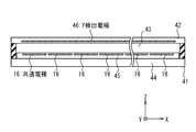
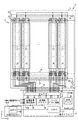
図2は、一実施形態における表示パネル2の構成を概略的に示す断面図であり、図3は、表示パネル2の構成を概略的に示す平面図である。以下の説明においては、XYZ直交座標系が導入される。X軸方向は、表示パネル2のゲート線が延伸する方向であり、Y軸方向は、ソース線が延伸する方向であり、Z軸方向は、表示パネル2の厚さ方向である。
FIG. 2 is a cross-sectional view schematically showing the configuration of the
図2を参照して、表示パネル2は、インセル構成の液晶表示パネルとして構成されており、TFT(thin film transistor)基板41と、対向基板42とを備えている。対向基板42は、TFT基板41と互いに対向するように配置され、TFT基板41と対向基板42との間には液晶43が満たされる。
With reference to FIG. 2, the
TFT基板41は、ガラス基板44と、その上に集積化された半導体回路45とを備えている。半導体回路45は、上述された表示回路11、ゲートドライバ回路12と、スイッチ回路15とを含んでいる(ただし、図2、図3には図示されない)。加えて、本実施形態では、半導体回路45が、複数の共通電極16を含んでいる。図3に図示されているように、共通電極16は、X軸方向に並んで配置されており、それぞれがY軸方向に延伸するように形成されている。TFT基板41に共通電極16が形成される構成は、例えば、国際公開WO2013/100088A1(特許文献2)に開示されているように、当業者に周知であることに留意されたい。
The
本実施形態では、表示パネル2が、インセル構成の液晶表示パネルとして構成されている。より具体的には、対向基板42が、複数のY検出電極46を含んでいる。図3に図示されているように、Y検出電極46は、それぞれがX軸方向に延伸するように形成されており、複数のY検出電極46がY軸方向に並んで配置されている。Y検出電極46は、表示パネル2に物体が接触したY軸方向の位置を検出するために用いられる。表示ドライバ3は、Y検出電極46のそれぞれの静電容量を検出し、検出した静電容量に基づいて表示パネル2に物体が接触したY軸方向の位置を検出するように構成される。
In the present embodiment, the
加えて、共通電極16が、各画素回路による液晶43の駆動のみならず、表示パネル2に物体が接触したX軸方向の位置を検出するために用いられる。即ち、共通電極16は、図1に図示されている構成のタッチ検出電極群14のタッチ検出電極としても用いられる。表示ドライバ3は、共通電極16に共通電圧VCOMを供給すると共に、共通電極16のそれぞれの静電容量を検出し、検出した静電容量に基づいて表示パネル2に物体が接触したX軸方向の位置を検出するように構成される。なお、対向基板42は、更に他の構成要素、例えば、カラーフィルター及び偏光板を含み得るが、図2、図3には図示されていない。
In addition, the
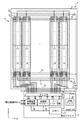
図4は、本実施形態における表示装置1の構成の詳細を示す図である。
FIG. 4 is a diagram showing details of the configuration of the
上述のように、表示パネル2は、表示回路11と、ゲートドライバ回路12(図4には図示されない)と、スイッチ回路15とを備えている。図4には、表示回路11に含まれる構成要素のうち、共通電極16及びソース線17のみが図示されている。ソース線17は、共通電極16より下方(即ち、共通電極16とガラス基板44の間)に位置しており、このため、図4においては、ソース線17の共通電極16の背後に位置する部分が破線で示されている。
As described above, the
図5は、図4の表示パネル2の拡大図である。図4の構成では、ソース線17は、ソース入力端子13に一対一で対応しており、ソース線17は、ソース入力端子13にそれぞれに接続されている。スイッチ回路15は、ソース入力端子13にそれぞれに接続されたスイッチ18を有している。本実施形態では、各共通電極16は、複数のソース線17に対応しており(即ち、各共通電極16の下方に複数のソース線17が配置されており)、各共通電極16は、対応するソース線17に接続されているソース入力端子13にスイッチ18を介して接続されている。スイッチ回路15は、表示ドライバ3に近い位置(表示ドライバ3と共通電極16の間の位置)に設けられており、スイッチ回路15の各スイッチ18は、対応するソース線17のソース入力端子13に近い方の端に接続されている。
FIG. 5 is an enlarged view of the
表示パネル2は、更に、スイッチ回路19と、VCOM入力端子(共通電圧入力端子)20と、VCOMスイッチ回路21、22と、スイッチ制御端子23と、インバータ24、25とを備えている。
The
スイッチ回路19は、各共通電極16を、それに対応するソース線17に電気的に接続する機能を有している。スイッチ回路19は、表示ドライバ3から離れた位置(共通電極16を挟んで表示ドライバ3に対して反対の位置)に設けられている。図5に図示されているように、スイッチ回路19は、各共通電極16と、それに対応するソース線17の間に接続されたスイッチ26を備えている。スイッチ回路19の各スイッチ26は、対応するソース線17のソース入力端子13から離れている方の端に接続されている。
The
VCOM入力端子20とVCOMスイッチ回路21、22は、表示ドライバ3から受け取った共通電圧VCOMを各共通電極16に供給する機能を有している。詳細には、VCOM入力端子20は、表示ドライバ3から共通電圧VCOMを受け取る。VCOMスイッチ回路21、22は、VCOM入力端子20を各共通電極16に電気的に接続し、又は、電気的に切り離す。VCOMスイッチ回路21は、各共通電極16の−Y方向の端とVCOM入力端子20の間に接続されたスイッチ27を有しており、VCOMスイッチ回路22は、各共通電極16の+Y方向の端とVCOM入力端子20の間に接続されたスイッチ28を有している。VCOMスイッチ回路21は、表示ドライバ3に近い位置(表示ドライバ3と共通電極16の間の位置)に設けられているのに対し、VCOMスイッチ回路22は、表示ドライバ3から離れた位置(共通電極16を挟んで表示ドライバ3に対して反対の位置)に設けられている。
スイッチ制御端子23及びインバータ24、25は、スイッチ回路15、19及びVCOMスイッチ回路21、22を制御するために用いられる。スイッチ制御端子23は、表示ドライバ3からスイッチ制御信号touch_selを受け取り、スイッチ回路15、19に供給する。インバータ24、25は、スイッチ制御信号touch_selの反転信号を生成し、生成した反転信号をVCOMスイッチ回路21、22のスイッチ27、28に供給する。スイッチ回路15、19のスイッチ18、26と、VCOMスイッチ回路21、22のスイッチ27、28とは、スイッチ制御信号touch_selに応じて排他的にターンオンされる。詳細には、スイッチ制御信号touch_selがアサートされると、スイッチ回路15、19のスイッチ18、26がターンオンされ、VCOMスイッチ回路21、22のスイッチ27、28がターンオフされる。一方、スイッチ制御信号touch_selがネゲートされると、スイッチ回路15、19のスイッチ18、26がターンオフされ、VCOMスイッチ回路21、22のスイッチ27、28がターンオンされる。
The
図4を再度に参照して、表示ドライバ3は、ソース出力端子31と、パネルインタフェース回路32と、ソースドライバ回路33と、セレクタ35と、静電容量検出回路36と、コントローラ37とを備えている。ただし、パネルインタフェース回路32は、図4には図示されていない。ソース出力端子31と、パネルインタフェース回路32と、ソースドライバ回路33と、セレクタ35と、静電容量検出回路36と、コントローラ37とは、モノリシックに(即ち、同一の半導体チップに)集積化されている。
With reference to FIG. 4 again, the
静電容量検出回路36とコントローラ37とは、図1の構成のタッチ検出回路34に対応する構成要素である。静電容量検出回路36の入力は、セレクタ35に接続されている。図4の構成では、静電容量検出回路36が、Y検出電極46に接続される入力も備えている。静電容量検出回路36は、その入力に接続された導電体の静電容量を示す静電容量データを生成するように構成されている。共通電極16がセレクタ35を介して静電容量検出回路36の入力に接続されると、共通電極16の静電容量を検出する。加えて、静電容量検出回路36は、Y検出電極46の静電容量及び共通電極16とY検出電極46の間に形成された静電容量も検出するように構成されている。コントローラ37は、表示ドライバ3の動作、特に、表示パネル2のソース線17を駆動する動作と、タッチイベントを検出する動作を制御する。タッチイベントの検出においては、コントローラ37は、静電容量検出回路36から受け取った静電容量データに基づいて(即ち、静電容量検出回路36によって検出された静電容量に基づいて)、表示パネル2に物体が接触した位置を算出する。
The
加えて、図4の構成では、表示ドライバ3は、送信側ドライバ38とVCOMアンプ39とを備えている。送信側ドライバ38は、相互容量方式でタッチイベントの検出を行う場合に用いられる。相互容量方式でタッチイベントの検出を行う場合、共通電極16が送信側電極として用いられ、Y検出電極46が受信側電極として用いられる。送信側ドライバ38は、相互容量方式でタッチイベントの検出を行うときに送信側電極として用いられる共通電極16を駆動する。VCOMアンプ39は、共通電圧VCOMを発生し、発生した共通電圧VCOMを表示パネル2のVCOM入力端子20に供給する共通電圧生成回路として動作する。
In addition, in the configuration of FIG. 4, the
図4の構成では、セレクタ35が、ソース出力端子31を、3つの接続先:ソースドライバ回路33、静電容量検出回路36、及び、送信側ドライバ38のうちのいずれかに選択的に接続する動作を行うことに留意されたい。
In the configuration of FIG. 4, the
続いて、図4、図5に図示されている構成の表示装置1の動作について説明する。図4に図示されている表示装置1は、3つの動作:(1)表示回路11の各画素回路を駆動する駆動動作、(2)自己容量方式によるタッチイベントの検出、及び、(3)相互容量方式によるタッチイベントの検出に対応している。以下、それぞれの動作について説明する。
Subsequently, the operation of the
駆動動作が行われる場合、表示装置1の表示ドライバ3は、下記のように動作する。表示ドライバ3のコントローラ37は、スイッチ制御信号touch_selをネゲートする。スイッチ制御信号touch_selのネゲートに応答して、VCOMスイッチ回路21、22の各スイッチ27、28がターンオンされ、スイッチ回路15、19の各スイッチ18、26がターンオフされる。これにより、各共通電極16がVCOMアンプ39に接続される。VCOMアンプ39は、各共通電極16に共通電圧VCOMを供給する。一方、セレクタ35は、コントローラ37による制御の下、ソース出力端子31をソースドライバ回路33の出力に接続する。これにより、表示パネル2の各ソース線17がソースドライバ回路33の出力に接続される。ソースドライバ回路33は、セレクタ35を介してソース出力端子31からソース信号を表示パネル2の各ソース線17に供給する。このような動作により、表示回路11の各画素回路が駆動される。
When the drive operation is performed, the
一方、自己容量方式によるタッチイベント検出が行われる場合、表示ドライバ3は、下記のように動作する。表示ドライバ3のコントローラ37は、スイッチ制御信号touch_selをアサートする。スイッチ制御信号touch_selのアサートに応答して、スイッチ回路15、19の各スイッチ18、26がターンオンされ、VCOMスイッチ回路21、22の各スイッチ27、28がターンオフされる。これにより、表示パネル2において各共通電極16がソース入力端子13に接続される。一方、セレクタ35は、コントローラ37による制御の下、ソース出力端子31を静電容量検出回路36の入力に接続する。これにより、表示パネル2の各共通電極16が静電容量検出回路36の入力に接続される。静電容量検出回路36は、各共通電極16の静電容量と各Y検出電極46の静電容量を検出し、検出した静電容量を示す静電容量データを生成する。コントローラ37は、静電容量検出回路36から受け取った静電容量データに基づいてタッチイベントの検出を行う。より具体的には、コントローラ37は、各共通電極16の静電容量に基づいて表示パネル2に物体が接触したX軸方向における位置を算出し、各Y検出電極46の静電容量に基づいて、表示パネル2に物体が接触したY軸方向における位置を算出する。
On the other hand, when the touch event is detected by the self-capacity method, the
また、相互容量方式によるタッチイベント検出が行われる場合、表示ドライバ3は、下記のように動作する。表示ドライバ3のコントローラ37は、スイッチ制御信号touch_selをアサートする。スイッチ制御信号touch_selのアサートに応答して、スイッチ回路15、19の各スイッチ18、26がターンオンされ、VCOMスイッチ回路21、22の各スイッチ27、28がターンオフされる。これにより、表示パネル2において各共通電極16がソース入力端子13に接続される。一方、セレクタ35は、コントローラ37による制御の下、ソース出力端子31を送信側ドライバ38の出力に接続する。送信側ドライバ38は、セレクタ35を介してソース出力端子31から駆動電圧を表示パネル2の各共通電極16に供給して各共通電極16を駆動する。静電容量検出回路36は、各共通電極16と各Y検出電極46の間の静電容量を検出し、静電容量データを生成する。コントローラ37は、静電容量検出回路36から受け取った静電容量データに示されている各共通電極16と各Y検出電極46の間の静電容量に基づいて、表示パネル2に物体が接触した位置を算出する。
Further, when the touch event is detected by the mutual capacitance method, the
図4に図示されている表示装置1の構成では、共通電極16と静電容量検出回路36とを接続するための専用の外部接続端子を表示パネル2に設ける必要がない。したがって、共通電極16をタッチ検出電極として用いる構成の表示パネル2の外部接続端子の数を低減することができる。
In the configuration of the
なお、図4に図示されている表示装置1は、必ずしも、相互容量方式によるタッチイベント検出を行うように構成されなくてもよい。この場合、送信側ドライバ38を表示ドライバ3に設ける必要は無い。
The
図4に図示されている構成では、表示ドライバ3が、タッチイベントの検出に用いられる回路群(例えば、静電容量検出回路36及び送信側ドライバ38)と、ソース線17の駆動に用いられる回路群(例えば、ソースドライバ回路33)の両方を備えているが、タッチイベントの検出に用いられる回路群の少なくとも一部が、表示ドライバ3とは別の半導体チップに集積化されてもよい。図6、図7は、このような構成の表示装置1を示している。
In the configuration shown in FIG. 4, the
図6は、表示装置1が、表示ドライバ3とは別に外部タッチコントローラ61を備えている構成を図示している。図6の構成では、静電容量検出回路62と送信側ドライバ63とコントローラ64とが外部タッチコントローラ61に集積化されている。
FIG. 6 illustrates a configuration in which the
静電容量検出回路62は、入力に接続されている導電体の静電容量を検出し、検出した静電容量を示す静電容量データを生成するように構成されている。静電容量検出回路62は、各共通電極16の静電容量、各Y検出電極46の静電容量、及び、各共通電極16と各Y検出電極46の間の静電容量を検出するために用いられる。
The capacitance detection circuit 62 is configured to detect the capacitance of the conductor connected to the input and generate capacitance data indicating the detected capacitance. The capacitance detection circuit 62 detects the capacitance of each
送信側ドライバ63は、相互容量方式でタッチイベントの検出を行う場合に送信側電極として用いられる共通電極16を駆動する。
The transmitting
コントローラ64は、タッチイベント検出を行う場合の動作タイミングを制御するタイミング制御信号を静電容量検出回路62、送信側ドライバ63及び表示ドライバ3のコントローラ37に供給する。加えて、コントローラ64は、静電容量検出回路62によって検出された静電容量(各共通電極16の静電容量、各Y検出電極46の静電容量、及び、各共通電極16と各Y検出電極46の間の静電容量)に基づいて表示パネル2に物体が接触した位置を算出する。表示ドライバ3には、静電容量検出回路62をセレクタ35に接続する接続配線62aと、送信側ドライバ63をセレクタ35に接続する接続配線63aとが設けられる。セレクタ35は、コントローラ37から受け取った制御信号に応じて、静電容量検出回路62に接続された接続配線62a、送信側ドライバ63に接続された接続配線63a、ソースドライバ回路33に接続された接続配線33aのいずれかにソース出力端子31を接続する。
The
図6の構成の表示装置1の動作は、静電容量検出回路36及び送信側ドライバ38の代わりに外部タッチコントローラ61の静電容量検出回路62及び送信側ドライバ63が用いられ、また、外部タッチコントローラ61のコントローラ64によって表示パネル2に物体が接触した位置が算出されることを除けば、図4の構成の表示装置1と同じである。
In the operation of the
図7は、表示装置1が、表示ドライバ3とは別に外部タッチコントローラ61Aを備えている構成を図示している。図7の構成では、静電容量検出回路36によって検出された静電容量に基づいて表示パネル2に物体が接触した位置を算出するコントローラ64が外部タッチコントローラ61Aに集積化されている。静電容量検出回路36と送信側ドライバ38は、表示ドライバ3に集積化されており、コントローラ64は、静電容量検出回路36及び送信側ドライバ38にデータ/制御バス64aを介して接続されている。コントローラ64は、静電容量検出回路36によって検出された静電容量(各共通電極16の静電容量、各Y検出電極46の静電容量、及び、各共通電極16と各Y検出電極46の間の静電容量)を示す静電容量データをデータ/制御バス64aを介して静電容量検出回路36から受け取り、受け取った静電容量データに基づいて(即ち、静電容量検出回路36によって検出された静電容量に基づいて)表示パネル2に物体が接触した位置を算出する。また、コントローラ64は、静電容量検出回路36と送信側ドライバ38とを制御する制御データをデータ/制御バス64aを介して送信する。
FIG. 7 illustrates a configuration in which the
図7の構成の表示装置1の動作は、表示ドライバ3のコントローラ37の代わりに外部タッチコントローラ61Aのコントローラ64によって表示パネル2に物体が接触した位置が算出されることを除けば、図4の構成の表示装置1と同じである。
The operation of the
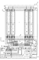
図8は、他の実施形態の表示装置1を図示している。図8に図示された表示装置1では、表示パネル2の構成が図4に図示された表示装置1から変更されている。具体的には、図8の構成では、表示ドライバ3から離れた位置(共通電極16を挟んで表示ドライバ3に対して反対の位置)に設けられているスイッチ回路19及びVCOMスイッチ回路22が表示パネル2から除去されている。図8の構成の表示装置1では、共通電極16とソース線17との間の電気的接続、及び、共通電極16とVCOM入力端子20との間の電気的接続が弱くなるが、本質的には、図4に図示された表示装置1と同様に動作する。図8の構成は、スイッチ回路19及びVCOMスイッチ回路22を設ける領域が不要であり、表示パネル2の面積の低減に有用である。
FIG. 8 illustrates the
図9は、更に他の実施形態の表示装置1を図示している。図9の構成では、(共通電極16ではなく)ソース線17が、タッチ検出電極として用いられる。これに伴い、表示パネル2からスイッチ回路15、19が除去されている。
FIG. 9 illustrates the
図9の構成の表示装置1では、駆動動作が行われる場合、表示ドライバ3が下記のように動作する。表示ドライバ3のコントローラ37は、スイッチ制御信号touch_selをネゲートする。スイッチ制御信号touch_selのネゲートに応答して、VCOMスイッチ回路21の各スイッチ27がターンオンされ、これにより、各共通電極16がVCOMアンプ39に接続される。VCOMアンプ39は、各共通電極16に共通電圧VCOMを供給する。一方、セレクタ35は、コントローラ37による制御の下、ソース出力端子31をソースドライバ回路33の出力に接続する。これにより、表示パネル2の各ソース線17がソースドライバ回路33の出力に接続される。ソースドライバ回路33は、セレクタ35を介してソース出力端子31からソース信号を表示パネル2の各ソース線17に供給する。このような動作により、表示回路11の各画素回路が駆動される。
In the
一方、自己容量方式によるタッチイベント検出が行われる場合、表示ドライバ3は、下記のように動作する。表示ドライバ3のコントローラ37は、スイッチ制御信号touch_selをアサートする。スイッチ制御信号touch_selのアサートに応答して、VCOMスイッチ回路21の各スイッチ27がターンオフされる。一方、セレクタ35は、コントローラ37による制御の下、ソース出力端子31を静電容量検出回路36の入力に接続する。これにより、表示パネル2の各ソース線17が静電容量検出回路36の入力に接続される。静電容量検出回路36は、各ソース線17と各Y検出電極46の静電容量を検出し、検出した静電容量を示す静電容量データを生成する。コントローラ37は、静電容量検出回路36から受け取った静電容量データに基づいて(即ち、各ソース線17と各Y検出電極46の静電容量に基づいて)、タッチイベントの検出を行う。より具体的には、コントローラ37は、各ソース線17の静電容量に基づいて表示パネル2に物体が接触したX軸方向における位置を算出し、各Y検出電極46の静電容量に基づいて、表示パネル2に物体が接触したY軸方向における位置を算出する。
On the other hand, when the touch event is detected by the self-capacity method, the
また、相互容量方式によるタッチイベント検出が行われる場合、表示ドライバ3は、下記のように動作する。表示ドライバ3のコントローラ37は、スイッチ制御信号touch_selをアサートする。スイッチ制御信号touch_selのアサートに応答して、VCOMスイッチ回路21の各スイッチ27がターンオフされる。一方、セレクタ35は、コントローラ37による制御の下、ソース出力端子31を送信側ドライバ38の出力に接続する。送信側ドライバ38は、セレクタ35を介してソース出力端子31から駆動電圧を表示パネル2の各ソース線17に供給する。静電容量検出回路36は、各ソース線17と各Y検出電極46の間の静電容量を検出し、検出した静電容量を示す静電容量データを生成する。コントローラ37は、静電容量検出回路36から受け取った静電容量データに基づいて(即ち、各ソース線17と各Y検出電極46の間の静電容量に基づいて)、表示パネル2に物体が接触した位置を算出する。
Further, when the touch event is detected by the mutual capacitance method, the
図9の構成では、ソース線17がタッチ検出電極としても用いられるため、ソース線17に接続されるソース入力端子13とは別にタッチ検出電極に接続される外部接続端子を表示パネル2に設ける必要がない。したがって、インセル構成の表示パネル2の外部接続端子の数を低減することができる。
In the configuration of FIG. 9, since the
図10は、更に他の実施形態の表示装置1を図示している。図10に図示されている表示装置1の構成は、図8に図示されている表示装置1の構成と類似しているが、時分割駆動によってソース線17が駆動される点で相違する。より具体的には、表示パネル2の1つのソース入力端子13に対して3本のソース線17が設けられており、該3本のソース線17は、それぞれ、異なる色の副画素の画素回路に接続されている。
FIG. 10 illustrates the
図11に図示されているように、各ソース入力端子13に対応する3本のソース線17は、赤色の副画素に対応するソース線17rと、緑色の副画素に対応するソース線17gと、青色の副画素に対応するソース線17bとで構成されている。ソース線17rに沿って赤色の副画素の画素回路(図示されない)が配置され、赤色の副画素の画素回路は、ソース線17rに接続される。同様に、ソース線17gに沿って緑色の副画素の画素回路(図示されない)が配置され、緑色の副画素の画素回路は、ソース線17gに接続される。また、ソース線17bに沿って青色の副画素の画素回路(図示されない)が配置され、青色の副画素の画素回路は、ソース線17bに接続される。
As shown in FIG. 11, the three
図10の構成では、時分割駆動を行うために、表示パネル2にソース線選択回路29が設けられる。図11に図示されているように、ソース線選択回路29は、赤色の副画素に対応するソース線17rとソース入力端子13との間に接続されたスイッチ30rと、緑色の副画素に対応するソース線17gとソース入力端子13との間に接続されたスイッチ30gと、青色の副画素に対応するソース線17bとソース入力端子13との間に接続されたスイッチ30bとを備えている。スイッチ30r、30g、30bには、それぞれ、表示ドライバ3のコントローラ37によって生成された赤色選択信号R_sel、緑色選択信号G_sel、青色選択信号B_selが供給される。スイッチ30rは、赤色選択信号R_selに応答して動作し、スイッチ30gは、緑色選択信号G_selに応答して動作し、スイッチ30bは、青色選択信号B_selに応答して動作する。表示回路11の各画素回路の駆動においては、スイッチ30r、30g、30bは、赤色選択信号R_sel、緑色選択信号G_sel、青色選択信号B_selによる制御の下、時分割的にターンオンされる。
In the configuration of FIG. 10, a source
続いて、図10、図11に図示されている構成の表示装置1の動作について説明する。
Subsequently, the operation of the
駆動動作が行われる場合、表示装置1の表示ドライバ3は、下記のように動作する。表示ドライバ3のコントローラ37は、スイッチ制御信号touch_selをネゲートする。スイッチ制御信号touch_selのネゲートに応答して、VCOMスイッチ回路21の各スイッチ27がターンオンされ、スイッチ回路15の各スイッチ18がターンオフされる。これにより、各共通電極16がVCOMアンプ39に接続される。VCOMアンプ39は、各共通電極16に共通電圧VCOMを供給する。更に、セレクタ35は、コントローラ37による制御の下、ソース出力端子31をソースドライバ回路33の出力に接続する。
When the drive operation is performed, the
赤色の副画素の画素回路を駆動する場合、コントローラ37は、赤色選択信号R_selをアサートし、緑色選択信号G_sel、青色選択信号B_selをネゲートする。これにより、スイッチ30rがターンオンされ、赤色の副画素に対応するソース線17rがソース入力端子13に接続される。ソースドライバ回路33は、セレクタ35を介してソース信号を表示パネル2のソース入力端子13に供給する。このような動作により、ソース線17rに接続されている画素回路(即ち、赤色の副画素の画素回路)にソース信号が供給される。
When driving the pixel circuit of the red sub-pixel, the
同様に、緑色の副画素の画素回路を駆動する場合、コントローラ37は、緑色選択信号G_selをアサートし、青色選択信号B_sel、赤色選択信号R_selをネゲートする。これにより、スイッチ30gがターンオンされ、緑色の副画素に対応するソース線17gがソース入力端子13に接続される。ソースドライバ回路33は、セレクタ35を介してソース信号を表示パネル2のソース入力端子13に供給する。このような動作により、ソース線17gに接続されている画素回路(即ち、緑色の副画素の画素回路)にソース信号が供給される。
Similarly, when driving the pixel circuit of the green sub-pixel, the
また、青色の副画素の画素回路を駆動する場合、コントローラ37は、青色選択信号B_selをアサートし、赤色選択信号R_sel、緑色選択信号G_selをネゲートする。これにより、スイッチ30bがターンオンされ、青色の副画素に対応するソース線17bがソース入力端子13に接続される。ソースドライバ回路33は、セレクタ35を介してソース信号を表示パネル2のソース入力端子13に供給する。このような動作により、ソース信号がソース線17bに接続されている画素回路(即ち、青色の副画素の画素回路)に供給される。以上に述べられた動作により、表示回路11の各画素回路が駆動される。
When driving the pixel circuit of the blue sub-pixel, the
一方、自己容量方式によるタッチイベント検出が行われる場合、表示ドライバ3は、下記のように動作する。表示ドライバ3のコントローラ37は、スイッチ制御信号touch_selをアサートする。スイッチ制御信号touch_selのアサートに応答して、スイッチ回路15の各スイッチ18がターンオンされ、VCOMスイッチ回路21の各スイッチ27がターンオフされる。これにより、表示パネル2において各共通電極16がソース入力端子13に接続される。一方、セレクタ35は、コントローラ37による制御の下、ソース出力端子31を静電容量検出回路36の入力に接続する。これにより、表示パネル2の各共通電極16が静電容量検出回路36の入力に接続される。静電容量検出回路36は、各共通電極16と各Y検出電極46の静電容量を検出し、検出した静電容量を示す静電容量データを生成する。コントローラ37は、静電容量検出回路36から受け取った静電容量データに基づいてタッチイベントの検出を行う。より具体的には、コントローラ37は、各共通電極16の静電容量に基づいて表示パネル2に物体が接触したX軸方向における位置を算出し、各Y検出電極46の静電容量に基づいて、表示パネル2に物体が接触したY軸方向における位置を算出する。
On the other hand, when the touch event is detected by the self-capacity method, the
また、相互容量方式によるタッチイベント検出が行われる場合、表示ドライバ3は、下記のように動作する。表示ドライバ3のコントローラ37は、スイッチ制御信号touch_selをアサートする。スイッチ制御信号touch_selのアサートに応答して、スイッチ回路15の各スイッチ18がターンオンされ、VCOMスイッチ回路21の各スイッチ27がターンオフされる。これにより、表示パネル2において各共通電極16がソース入力端子13に接続される。一方、セレクタ35は、コントローラ37による制御の下、ソース出力端子31を送信側ドライバ38の出力に接続する。送信側ドライバ38は、セレクタ35を介してソース出力端子31から駆動電圧を表示パネル2の各共通電極16に供給する。静電容量検出回路36は、各共通電極16と各Y検出電極46の間の静電容量を検出し、検出した静電容量を示す静電容量データを生成する。コントローラ37は、静電容量検出回路36から受け取った静電容量データに基づいて(即ち、各共通電極16と各Y検出電極46の間の静電容量に基づいて)、表示パネル2に物体が接触した位置を算出する。
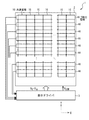
Further, when the touch event is detected by the mutual capacitance method, the
図12は、更に他の実施形態の表示装置1を図示している。図4に図示されている構成では、Y軸方向に延伸する形状の共通電極16がX軸方向に並べられていたが、図12に図示されている構成では、共通電極51が行列に、即ち、複数の行及び複数の列に並んで配置されている。共通電極51は、各行においてX軸方向に並んで配置されており、各列においてY軸方向に並んで配置されている。Y軸方向に延伸するソース線17がX軸方向に並んで配置され、ソース線17は、ソース入力端子13にそれぞれに接続されている。各列の共通電極51には複数のソース線17が交差している。
FIG. 12 illustrates the
本実施形態においては、行列に配置されている共通電極51がタッチ検出電極として用いられる。留意すべきことは、タッチ検出電極として用いられる共通電極51が行列に配置されている図12の構成は、自己容量方式によるタッチイベントの検出に好適であるということである。上述の実施形態のように、共通電極16とY検出電極46とが交差する構成の表示パネル2において自己容量方式によるタッチイベントの検出を行う構成では、複数個所で物体が表示パネル2に接触したときに、いわゆる「ゴースト」の問題が生じ得る。本実施形態では、タッチ検出電極として用いられる共通電極51が行列に並んで配置されているので、「ゴースト」の問題は生じない。
In this embodiment, the
このため、図12の構成の表示装置1では、相互容量方式によるタッチイベントの検出が行われない。本実施形態では、表示ドライバ3は、相互容量方式によるタッチイベントの検出に対応する構成を有しておらず、このため、送信側ドライバ38を備えていない。ただし、後述のように、共通電極51が行列に並んで配置されている構成においても、表示装置1が、相互容量方式によるタッチイベントの検出に対応するように構成されてもよい。
Therefore, the
図13は、図12に図示されている表示装置1の表示パネル2の構成の詳細を示している。表示パネル2には、各共通電極51についてコンタクト52、スイッチ53、54が設けられている。コンタクト52は、対応する共通電極51に接続されている。加えて、表示パネル2は、インバータ24とVCOMライン55とを備えている。インバータ24は、その入力がスイッチ制御端子23に接続されており、スイッチ制御信号touch_selの反転信号を生成する。VCOMライン55は、VCOM入力端子20に接続されている。図12、図13に図示されている構成では、VCOMライン55は、Y軸方向に延伸するように設けられている。
FIG. 13 shows the details of the configuration of the
スイッチ53は、各共通電極51に対応するソース線17(各共通電極51と交差するソース線17)のうちの1本のソース線17と、コンタクト52の間に接続されている。各共通電極51に接続されているスイッチ53は、共通電極51を(ソース線17を介して)対応するソース入力端子13に電気的に接続する機能を有している。スイッチ53は、スイッチ制御信号touch_selに応答して動作する。
The
スイッチ54は、VCOMライン55と、コンタクト52の間に接続されている。図13の構成では、全ての共通電極51は、それぞれに対応するスイッチ54を介してVCOMライン55に共通に接続されている。後述されるように、表示ドライバ3からVCOM入力端子20に供給された共通電圧VCOMは、VCOMライン55及びスイッチ54を介して各共通電極51に供給される。スイッチ54は、インバータ24によって生成されるスイッチ制御信号touch_selの反転信号に応答して動作する。
The
なお、図13には、各共通電極51について1つのスイッチ53が設けられ、当該スイッチ53を介して各共通電極51が1本のソース線17に接続される構成が図示されているが、各共通電極51について複数のスイッチ53が設けられ、各共通電極51が、該複数のスイッチ53を介して複数のソース線17に接続されていてもよい。ただし、この場合でも、各ソース線17についてみれば、各ソース線17にスイッチ53を介して接続される共通電極51の数は1つであることに留意されたい。
Note that FIG. 13 shows a configuration in which one
続いて、図12、図13に図示されている構成の表示装置1の動作について説明する。
Subsequently, the operation of the
駆動動作が行われる場合、表示装置1の表示ドライバ3は、下記のように動作する。表示ドライバ3のコントローラ37は、スイッチ制御信号touch_selをネゲートする。スイッチ制御信号touch_selのネゲートに応答して、各共通電極51に対応するスイッチ54がターンオンされ、各共通電極51に対応するスイッチ53がターンオフされる。これにより、各共通電極51がVCOMアンプ39に接続される。VCOMアンプ39は、各共通電極51に共通電圧VCOMを供給する。更に、セレクタ35は、コントローラ37による制御の下、ソース出力端子31をソースドライバ回路33の出力に接続する。ソースドライバ回路33は、セレクタ35を介してソース出力端子31からソース信号を表示パネル2の各ソース線17に供給する。このような動作により、表示回路11の各画素回路が駆動される。
When the drive operation is performed, the
一方、自己容量方式によるタッチイベント検出が行われる場合、表示ドライバ3は、下記のように動作する。表示ドライバ3のコントローラ37は、スイッチ制御信号touch_selをアサートする。スイッチ制御信号touch_selのアサートに応答して、各共通電極51に対応するスイッチ53がターンオンされ、各共通電極51に対応するスイッチ54がターンオフされる。これにより、表示パネル2において各共通電極51が対応するソース線17を介して対応するソース入力端子13に接続される。一方、セレクタ35は、コントローラ37による制御の下、ソース出力端子31を静電容量検出回路36の入力に接続する。これにより、表示パネル2の各共通電極51が静電容量検出回路36の入力に接続される。静電容量検出回路36は、各共通電極51の静電容量を検出し、検出した静電容量を示す静電容量データを生成する。コントローラ37は、静電容量検出回路36から受け取った静電容量データに基づいて(即ち、各共通電極51の静電容量に基づいて)、タッチイベントの検出を行う。より具体的には、コントローラ37は、各共通電極51の静電容量に基づいて表示パネル2に物体が接触した位置を算出する。
On the other hand, when the touch event is detected by the self-capacity method, the
上述のように、共通電極51が行列に並んで配置されている構成においても、表示装置1が、相互容量方式によるタッチイベントの検出に対応するように構成されてもよい。図14、図15は、このような場合の表示装置1の構成を示している。図14に図示されているように、表示パネル2のY検出電極46は、共通電極51の各行に対応するように設けられており、対応する行の共通電極51と交差するように設けられている。加えて、表示ドライバ3に送信側ドライバ38が設けられる。
As described above, even in the configuration in which the
相互容量方式によるタッチイベント検出が行われる場合、表示ドライバ3は、下記のように動作する。表示ドライバ3のコントローラ37は、スイッチ制御信号touch_selをアサートする。スイッチ制御信号touch_selのアサートに応答して、各共通電極51に対応するスイッチ53がターンオンされ、各共通電極51に対応するスイッチ54がターンオフされる。これにより、表示パネル2において各共通電極51が対応するソース線17を介して対応するソース入力端子13に接続される。一方、セレクタ35は、コントローラ37による制御の下、ソース出力端子31を送信側ドライバ38の出力に接続する。送信側ドライバ38は、セレクタ35を介してソース出力端子31から駆動電圧を表示パネル2の各共通電極51に供給する。静電容量検出回路36は、各共通電極51と各Y検出電極46の間の静電容量を検出し、検出した静電容量を示す静電容量データを生成する。コントローラ37は、静電容量検出回路36から受け取った静電容量データに基づいて(即ち、各共通電極51と各Y検出電極46の間の静電容量に基づいて)、表示パネル2に物体が接触した位置を算出する。
When the touch event is detected by the mutual capacitance method, the
図12〜図15に図示されている構成では、全ての共通電極51がスイッチ54を介してVCOMライン55に接続されているが、図16に図示されているように、共通電極51の各列に沿ってVCOMライン56が設けられてもよい。VCOMライン56は、VCOM入力端子20に接続され、共通電圧VCOMを各共通電極51に供給するために用いられる。
In the configuration shown in FIGS. 12 to 15, all the
図17は、この場合の表示パネル2の構成を示している。各共通電極51について接続ノード57が設けられ、各VCOMライン56は、対応する共通電極51の列の接続ノード57に接続される。図16、図17に図示された構成の表示装置1の動作が、共通電圧VCOMを各共通電極51に供給する経路が異なるだけで図14、図15に図示された構成の表示装置1と本質的には同一であることは当業者には容易に理解されよう。
FIG. 17 shows the configuration of the
図18は、更に他の実施形態の表示装置1を図示している。図18の構成の表示装置1では、図14、図15に図示されている構成の表示装置1と同様に、共通電極51が行列に配置されているが、時分割駆動によってソース線17が駆動される点で相違する。より具体的には、表示パネル2の1つのソース入力端子13に対して3本のソース線17が設けられており、該3本のソース線17は、それぞれ、異なる色の副画素の画素回路に接続されている。
FIG. 18 illustrates the
図19に図示されているように、各ソース入力端子13に対応する3本のソース線17は、赤色の副画素に対応するソース線17rと、緑色の副画素に対応するソース線17gと、青色の副画素に対応するソース線17bとで構成されている。ソース線17rに沿って赤色の副画素の画素回路(図示されない)が配置され、赤色の副画素の画素回路は、ソース線17rに接続される。同様に、ソース線17gに沿って緑色の副画素の画素回路(図示されない)が配置され、緑色の副画素の画素回路は、ソース線17gに接続される。また、ソース線17bに沿って青色の副画素の画素回路(図示されない)が配置され、青色の副画素の画素回路は、ソース線17bに接続される。
As shown in FIG. 19, the three
時分割駆動を行うために、表示パネル2にソース線選択回路29が設けられる。ソース線選択回路29は、赤色の副画素に対応するソース線17rとソース入力端子13との間に接続されたスイッチ30rと、緑色の副画素に対応するソース線17gとソース入力端子13との間に接続されたスイッチ30gと、青色の副画素に対応するソース線17bとソース入力端子13との間に接続されたスイッチ30bとを備えている。スイッチ30r、30g、30bには、それぞれ、表示ドライバ3のコントローラ37によって生成された赤色選択信号R_sel、緑色選択信号G_sel、青色選択信号B_selが供給される。スイッチ30rは、赤色選択信号R_selに応答して動作し、スイッチ30gは、緑色選択信号G_selに応答して動作し、スイッチ30bは、青色選択信号B_selに応答して動作する。
A source
加えて、ソース入力端子13のそれぞれに対応して接続ライン58が設けられる。接続ライン58は、各ソース入力端子13に対応する3本のソース線17r、17g、17bに沿って設けられる。共通電極51の各列について複数の接続ライン58が設けられており、各共通電極51は、互いに異なる接続ライン58に接続されている。各共通電極51は、複数の接続ライン58に接続され得るが、各接続ライン58についてみれば、各接続ライン58に接続される共通電極51の数は1つであることに留意されたい。各接続ライン58は、スイッチ回路15のスイッチ18を介して対応するソース入力端子13に接続される。
In addition,
続いて、図18、図19に図示されている構成の表示装置1の動作について説明する。
駆動動作が行われる場合、表示装置1の表示ドライバ3は、下記のように動作する。表示ドライバ3のコントローラ37は、スイッチ制御信号touch_selをネゲートする。スイッチ制御信号touch_selのネゲートに応答して、VCOMスイッチ回路21の各スイッチ27がターンオンされ、スイッチ回路15の各スイッチ18がターンオフされる。これにより、各共通電極51がVCOMアンプ39に接続される。VCOMアンプ39は、各共通電極51に共通電圧VCOMを供給する。更に、セレクタ35は、コントローラ37による制御の下、ソース出力端子31をソースドライバ回路33の出力に接続する。
Subsequently, the operation of the
When the drive operation is performed, the
赤色の副画素の画素回路を駆動する場合、コントローラ37は、赤色選択信号R_selをアサートし、緑色選択信号G_sel、青色選択信号B_selをネゲートする。これにより、赤色の副画素に対応するソース線17rがソース入力端子13に接続される。ソースドライバ回路33は、セレクタ35を介してソース信号を表示パネル2のソース入力端子13に供給する。このような動作により、ソース線17rに接続されている画素回路(即ち、赤色の副画素の画素回路)にソース信号が供給される。
When driving the pixel circuit of the red sub-pixel, the
同様に、緑色の副画素の画素回路を駆動する場合、コントローラ37は、緑色選択信号G_selをアサートし、青色選択信号B_sel、赤色選択信号R_selをネゲートする。これにより、緑色の副画素に対応するソース線17gがソース入力端子13に接続される。ソースドライバ回路33は、セレクタ35を介してソース信号を表示パネル2のソース入力端子13に供給する。このような動作により、ソース線17gに接続されている画素回路(即ち、緑色の副画素の画素回路)にソース信号が供給される。
Similarly, when driving the pixel circuit of the green sub-pixel, the
また、青色の副画素の画素回路を駆動する場合、コントローラ37は、青色選択信号B_selをアサートし、赤色選択信号R_sel、緑色選択信号G_selをネゲートする。これにより、青色の副画素に対応するソース線17bがソース入力端子13に接続される。ソースドライバ回路33は、セレクタ35を介してソース信号を表示パネル2のソース入力端子13に供給する。このような動作により、ソース信号がソース線17bに接続されている画素回路(即ち、青色の副画素の画素回路)に供給される。以上に述べられた動作により、表示回路11の各画素回路が駆動される。
When driving the pixel circuit of the blue sub-pixel, the
一方、自己容量方式によるタッチイベント検出が行われる場合、表示ドライバ3は、下記のように動作する。表示ドライバ3のコントローラ37は、スイッチ制御信号touch_selをアサートする。スイッチ制御信号touch_selのアサートに応答して、スイッチ回路15の各スイッチ18がターンオンされ、VCOMスイッチ回路21の各スイッチ27がターンオフされる。これにより、表示パネル2において各共通電極51が対応するソース入力端子13に接続される。一方、セレクタ35は、コントローラ37による制御の下、ソース出力端子31を静電容量検出回路36の入力に接続する。これにより、表示パネル2の各共通電極51が静電容量検出回路36の入力に接続される。静電容量検出回路36は、各共通電極51の静電容量を検出し、検出した静電容量を示す静電容量データを生成する。コントローラ37は、静電容量検出回路36から受け取った静電容量データに基づいてタッチイベントの検出を行う。より具体的には、コントローラ37は、各共通電極51の静電容量に基づいて表示パネル2に物体が接触した位置を算出する。
On the other hand, when the touch event is detected by the self-capacity method, the
また、相互容量方式によるタッチイベント検出が行われる場合、表示ドライバ3は、下記のように動作する。表示ドライバ3のコントローラ37は、スイッチ制御信号touch_selをアサートする。スイッチ制御信号touch_selのアサートに応答して、スイッチ回路15の各スイッチ18がターンオンされ、VCOMスイッチ回路21の各スイッチ27がターンオフされる。これにより、表示パネル2において各共通電極51が対応するソース入力端子13に接続される。一方、セレクタ35は、コントローラ37による制御の下、ソース出力端子31を送信側ドライバ38の出力に接続する。送信側ドライバ38は、セレクタ35を介してソース出力端子31から駆動電圧を表示パネル2の各共通電極51に供給する。静電容量検出回路36は、各共通電極51と各Y検出電極46の間の静電容量を検出し、検出した静電容量を示す静電容量データを生成する。コントローラ37は、静電容量検出回路36から受け取った静電容量データに基づいて(即ち、各共通電極51と各Y検出電極46の間の静電容量に基づいて)表示パネル2に物体が接触した位置を算出する。
Further, when the touch event is detected by the mutual capacitance method, the
図18、図19の構成では、ソース線17に加えて接続ライン58が設けられているが、その代わりに、各共通電極51にスイッチを個別に設ける必要が無いという利点がある。図12〜図17に図示されている構成では、共通電極51のアレイの中に表示回路11の各画素回路を避けながらスイッチ53、54を配置する必要がある。これは、表示パネル2のレイアウト設計を複雑化させ得る。一方、図18、図19の構成では、各共通電極51とソース入力端子13とを電気的に接続するスイッチ18が、ソース入力端子13の近傍にあるスイッチ回路15に集約されているので、レイアウト設計が容易になる。
In the configurations of FIGS. 18 and 19, the
以上には、本発明の実施形態が具体的に記述されているが、本発明は、上記の実施形態に限定されない。本発明が種々の変更と共に実施され得ることは、当業者には理解されよう。 Although the embodiments of the present invention are specifically described above, the present invention is not limited to the above embodiments. Those skilled in the art will appreciate that the present invention can be practiced with various modifications.
1 :表示装置
2 :表示パネル
3 :表示ドライバ
11 :表示回路
12 :ゲートドライバ回路
13 :ソース入力端子
14 :タッチ検出電極群
15 :スイッチ回路
16 :共通電極
17、17r、17g、17b:ソース線
18 :スイッチ
19 :スイッチ回路
20 :VCOM入力端子
21 :VCOMスイッチ回路
22 :VCOMスイッチ回路
23 :スイッチ制御端子
24、25:インバータ
26、27、28:スイッチ
29 :ソース線選択回路
30r、30g、30b:スイッチ
31 :ソース出力端子
32 :パネルインタフェース回路
33 :ソースドライバ回路
33a :接続配線
34 :タッチ検出回路
34a :接続配線
35 :セレクタ
36 :静電容量検出回路
37 :コントローラ
38 :送信側ドライバ
39 :VCOMアンプ
41 :TFT基板
42 :対向基板
43 :液晶
44 :ガラス基板
45 :半導体回路
46 :Y検出電極
51 :共通電極
52 :コンタクト
53、54:スイッチ
55、56:VCOMライン
57 :接続ノード
58 :接続ライン
61、61A:外部タッチコントローラ
62 :静電容量検出回路
62a :接続配線
63 :送信側ドライバ
63a :接続配線
64 :コントローラ
64a :制御バス
1: Display device 2: Display panel 3: Display driver 11: Display circuit 12: Gate driver circuit 13: Source input terminal 14: Touch detection electrode group 15: Switch circuit 16:
Claims (11)
前記表示パネルの前記ソース入力端子に接続されるソース出力端子と、
前記ソース入力端子に供給するソース信号を生成するように構成されたソースドライバ回路と、
静電容量検出回路に接続される接続配線と、
セレクタ
とを具備し、
前記静電容量検出回路は、前記接続配線と前記セレクタとを介して前記静電容量検出回路に接続された導電体の静電容量を示し、前記表示パネルに物体が接触するタッチイベントの検出に用いられる静電容量データを生成するように構成され、
前記セレクタは、前記ソースドライバ回路と前記接続配線とを含む複数の接続先のうちのいずれかに前記ソース出力端子を選択的に接続するように構成され、
前記ソースドライバ回路と前記接続配線と前記セレクタとが、同一の半導体チップに集積化された
表示ドライバ。 A display driver that has a plurality of source lines and a plurality of source input terminals, and drives a display panel configured such that each of the plurality of source lines is connected to one of the plurality of source input terminals. hand,
A source output terminal connected to the source input terminal of the display panel and
A source driver circuit configured to generate a source signal to be supplied to the source input terminal,
A connection wiring connected to the electrostatic capacitance detection circuit,
Equipped with a selector,
The capacitance detection circuit indicates the capacitance of a conductor connected to the capacitance detection circuit via the connection wiring and the selector, and is used for detecting a touch event in which an object touches the display panel. Configured to generate the capacitance data used,
The selector is configured to selectively connect the source output terminal to any of a plurality of connection destinations including the source driver circuit and the connection wiring .
A display driver in which the source driver circuit, the connection wiring, and the selector are integrated on the same semiconductor chip.
請求項1に記載の表示ドライバ。 The selector connects the source output terminal to the source driver circuit when a drive operation for supplying the source signal to the source input terminal of the display panel is performed, and when the touch event is detected, the selector is said. The display driver according to claim 1, wherein the source output terminal is configured to be connected to the connection wiring.
前記静電容量検出回路は、前記第2検出電極に接続され、
当該表示ドライバは、更に、送信側ドライバを備え、
相互容量方式によって前記表示パネルに物体が接触するタッチイベントの検出を行う場合、前記送信側ドライバは、前記第1検出電極に供給すべき駆動電圧を生成し、前記セレクタは、前記ソース出力端子を前記送信側ドライバに接続し、前記静電容量検出回路は、前記第1検出電極と前記第2検出電極の間の静電容量を検出して前記静電容量データを生成する
請求項1に記載の表示ドライバ。 The display panel includes a first detection electrode and a second detection electrode.
The capacitance detection circuit is connected to the second detection electrode and is connected to the second detection electrode.
The display driver also includes a sender driver.
If the mutual capacitance method for detecting a touch event object on the display panel is flush with, the transmitting-side driver generates a pre SL drive voltage to be supplied to the first detection electrode, the selector, the source output terminal 1 to the transmission side driver, and the capacitance detection circuit detects the capacitance between the first detection electrode and the second detection electrode to generate the capacitance data. The listed display driver.
前記複数のソース線に供給するソース信号を前記複数のソース入力端子に供給するソースドライバ回路と、
静電容量検出回路と、
前記静電容量検出回路に接続された接続配線と、
前記表示パネルに物体が接触するタッチイベントの検出を行うように構成されたコントローラと、
前記複数のソース入力端子を、前記ソースドライバ回路と前記接続配線とを含む複数の接続先に選択的に接続するように構成されたセレクタ
とを備え、
前記静電容量検出回路は、前記接続配線と前記セレクタとを介して前記静電容量検出回路に接続された導電体の静電容量を示し、前記コントローラにより前記タッチイベントの検出に用いられる静電容量データを生成するように構成され、
前記ソースドライバ回路と前記接続配線と前記セレクタとが、同一の半導体チップに集積化された
表示装置。 A display panel with multiple source lines and multiple source input terminals,
A source driver circuit that supplies source signals supplied to the plurality of source lines to the plurality of source input terminals, and
A capacitance detection circuit,
The connection wiring connected to the capacitance detection circuit and
A controller object has been configured to detect a touch event in contact before Symbol display panel,
A selector configured to selectively connect the plurality of source input terminals to a plurality of connection destinations including the source driver circuit and the connection wiring is provided.
The capacitance detection circuit indicates the capacitance of a conductor connected to the capacitance detection circuit via the connection wiring and the selector, and is used by the controller to detect the touch event. Configured to generate capacitive data,
A display device in which the source driver circuit, the connection wiring, and the selector are integrated on the same semiconductor chip.
複数の共通電極と、
前記複数の共通電極の各共通電極と、前記複数のソース入力端子のうちの前記各共通電極に対応する少なくとも一の対応ソース入力端子との間に接続された第1スイッチ
とを備え、
前記ソース信号を前記ソース線に供給する駆動動作が行われる場合、前記セレクタが前記複数のソース入力端子を前記ソースドライバ回路に接続し、前記第1スイッチが前記各共通電極と前記複数のソース入力端子とを電気的に切り離し、
前記タッチイベントの検出が行われる場合、前記セレクタが前記複数のソース入力端子を前記静電容量検出回路の入力に接続し、前記第1スイッチが前記各共通電極と前記対応ソース入力端子とを電気的に接続する
請求項4に記載の表示装置。 The display panel further
With multiple common electrodes,
A first switch connected between each common electrode of the plurality of common electrodes and at least one corresponding source input terminal corresponding to each of the common electrodes among the plurality of source input terminals is provided.
When a drive operation for supplying the source signal to the source line is performed, the selector connects the plurality of source input terminals to the source driver circuit, and the first switch connects the common electrodes and the plurality of source inputs. Electrically disconnect from the terminal
When the touch event is detected, the selector connects the plurality of source input terminals to the inputs of the capacitance detection circuit, and the first switch electrically connects the common electrodes and the corresponding source input terminals. The display device according to claim 4, wherein the display device is connected.
前記表示パネルが、更に、
前記共通電圧を前記共通電圧生成回路から受け取る共通電圧入力端子と、
前記共通電圧入力端子と前記複数の共通電極との間にそれぞれに接続された第3スイッチ
とを備え、
前記駆動動作が行われる場合、前記第3スイッチが、前記複数の共通電極と前記共通電圧入力端子とを電気的に接続し、
前記タッチイベントの検出が行われる場合、前記第3スイッチが、前記複数の共通電極と前記共通電圧入力端子とを電気的に切り離す
請求項5に記載の表示装置。 Further, it is provided with a common voltage generation circuit that generates a common voltage.
The display panel further
A common voltage input terminal that receives the common voltage from the common voltage generation circuit,
A third switch connected to each of the common voltage input terminal and the plurality of common electrodes is provided.
When the drive operation is performed, the third switch electrically connects the plurality of common electrodes and the common voltage input terminal.
The display device according to claim 5, wherein when the touch event is detected, the third switch electrically disconnects the plurality of common electrodes and the common voltage input terminal.
請求項5に記載の表示装置。 The display device according to claim 5, wherein the plurality of common electrodes are arranged side by side in a plurality of rows and a plurality of columns.
前記各共通電極は、前記複数の接続ラインのそれぞれが、前記複数の共通電極のうちの単一の共通電極に接続されるように、前記複数の接続ラインのうちの少なくとも一に接続され、
前記各共通電極と前記対応ソース入力端子の間に接続された前記第1スイッチが、前記複数の接続ラインのうち前記各共通電極が接続された接続ラインと前記対応ソース入力端子の間に接続されている
請求項7に記載の表示装置。 The display panel further comprises a plurality of connecting lines extending in the direction in which the source line extends.
Each of the common electrodes is connected to at least one of the plurality of connection lines such that each of the plurality of connection lines is connected to a single common electrode of the plurality of common electrodes.
The first switch connected between the common electrodes and the corresponding source input terminal is connected between the connection line to which the common electrodes are connected and the corresponding source input terminal among the plurality of connection lines. The display device according to claim 7.
前記表示パネルが、更に、
前記共通電圧を前記共通電圧生成回路から受け取る共通電圧入力端子と、
前記共通電圧入力端子と前記複数の接続ラインとの間にそれぞれに接続された第3スイッチ
とを備え、
前記駆動動作が行われる場合、前記第3スイッチが、前記複数の共通電極と前記共通電圧入力端子とを電気的に接続し、
前記タッチイベントの検出が行われる場合、前記第3スイッチが、前記複数の共通電極と前記共通電圧入力端子とを電気的に切り離す
請求項8に記載の表示装置。 Further, it is provided with a common voltage generation circuit that generates a common voltage.
The display panel further
A common voltage input terminal that receives the common voltage from the common voltage generation circuit,
A third switch connected to each of the common voltage input terminal and the plurality of connection lines is provided.
When the drive operation is performed, the third switch electrically connects the plurality of common electrodes and the common voltage input terminal.
The display device according to claim 8, wherein when the touch event is detected, the third switch electrically disconnects the plurality of common electrodes and the common voltage input terminal.
表示ドライバから前記複数のソース線に供給されるソース信号を受け取る複数のソース入力端子と、
複数の共通電極が複数の行及び複数の列に並んで配置されたアレイと、
前記アレイの中に設けられ、それぞれが、前記複数の共通電極の各共通電極と、前記複数のソース線のうちの前記各共通電極に交差する少なくとも一の対応ソース線との間に接続された複数の第1スイッチとを具備する
表示パネル。 With multiple source lines
A plurality of source input terminals that receive source signals supplied from the display driver to the plurality of source lines, and
An array in which multiple common electrodes are arranged side by side in multiple rows and columns ,
Provided in said array, each of which is connected between the respective common electrodes of said plurality of common electrodes, and at least one corresponding source line wherein you intersect each common electrode of the plurality of source lines display panel comprising a plurality of first switches.
共通電圧を表示ドライバから受け取る共通電圧入力端子と、
前記共通電圧入力端子と前記複数の共通電極との間にそれぞれに接続された第3スイッチ
とを備える
請求項10に記載の表示パネル。 In addition
The common voltage input terminal that receives the common voltage from the display driver,
The display panel according to claim 10, further comprising a third switch connected to each of the common voltage input terminal and the plurality of common electrodes.
Priority Applications (3)
| Application Number | Priority Date | Filing Date | Title |
|---|---|---|---|
| JP2016202870A JP6863707B2 (en) | 2016-10-14 | 2016-10-14 | Display driver, display device and display panel |
| US15/782,508 US20180107317A1 (en) | 2016-10-14 | 2017-10-12 | Device and method for driving a display panel |
| CN201710951554.3A CN107957809A (en) | 2016-10-14 | 2017-10-13 | For driving the apparatus and method of display panel |
Applications Claiming Priority (1)
| Application Number | Priority Date | Filing Date | Title |
|---|---|---|---|
| JP2016202870A JP6863707B2 (en) | 2016-10-14 | 2016-10-14 | Display driver, display device and display panel |
Publications (3)
| Publication Number | Publication Date |
|---|---|
| JP2018063666A JP2018063666A (en) | 2018-04-19 |
| JP2018063666A5 JP2018063666A5 (en) | 2019-11-21 |
| JP6863707B2 true JP6863707B2 (en) | 2021-04-21 |
Family
ID=61903865
Family Applications (1)
| Application Number | Title | Priority Date | Filing Date |
|---|---|---|---|
| JP2016202870A Active JP6863707B2 (en) | 2016-10-14 | 2016-10-14 | Display driver, display device and display panel |
Country Status (3)
| Country | Link |
|---|---|
| US (1) | US20180107317A1 (en) |
| JP (1) | JP6863707B2 (en) |
| CN (1) | CN107957809A (en) |
Families Citing this family (12)
| Publication number | Priority date | Publication date | Assignee | Title |
|---|---|---|---|---|
| JP2019079025A (en) * | 2017-10-19 | 2019-05-23 | シナプティクス インコーポレイテッド | Display device, voltage control method in display panel, and display driver |
| JP6995683B2 (en) | 2018-04-20 | 2022-01-17 | 株式会社ジャパンディスプレイ | Display device |
| WO2020049649A1 (en) * | 2018-09-05 | 2020-03-12 | 堺ディスプレイプロダクト株式会社 | Touch panel device and method for detecting contact position in touch panel device |
| US10861411B2 (en) | 2019-01-17 | 2020-12-08 | Sharp Kabushiki Kaisha | Display device |
| US10963116B2 (en) | 2019-01-17 | 2021-03-30 | Sharp Kabushiki Kaisha | Display device |
| US20230111433A1 (en) * | 2019-02-08 | 2023-04-13 | Tactual Labs Co. | Non-uniform electrode spacing with a bend sensor |
| US11429216B2 (en) | 2019-10-25 | 2022-08-30 | Nuvoton Technology Corporation | Control circuit and display apparatus utilizing the same |
| US11429222B2 (en) | 2019-10-25 | 2022-08-30 | Nuvoton Technology Corporation | Control circuit and display apparatus utilizing the same |
| TWI729541B (en) * | 2019-10-25 | 2021-06-01 | 新唐科技股份有限公司 | Control circuit and operation system |
| TWI818253B (en) * | 2019-10-25 | 2023-10-11 | 新唐科技股份有限公司 | Operation system |
| TWI775403B (en) * | 2021-03-12 | 2022-08-21 | 新唐科技股份有限公司 | Control circuit and display apparatus |
| CN115079853A (en) * | 2021-03-12 | 2022-09-20 | 新唐科技股份有限公司 | Control circuit and display device |
Family Cites Families (13)
| Publication number | Priority date | Publication date | Assignee | Title |
|---|---|---|---|---|
| US8760412B2 (en) * | 2009-02-02 | 2014-06-24 | Apple Inc. | Dual configuration for display data lines |
| US9552089B2 (en) * | 2013-08-07 | 2017-01-24 | Synaptics Incorporated | Capacitive sensing using a matrix electrode pattern |
| JP6375223B2 (en) * | 2014-01-31 | 2018-08-15 | 株式会社ジャパンディスプレイ | Display device with sensor and driving method thereof |
| JP2015191118A (en) * | 2014-03-28 | 2015-11-02 | シナプティクス・ディスプレイ・デバイス合同会社 | Electronic device and display driver |
| JP2015230400A (en) * | 2014-06-05 | 2015-12-21 | 株式会社ジャパンディスプレイ | Display device |
| KR101648571B1 (en) * | 2014-07-16 | 2016-08-18 | 엘지디스플레이 주식회사 | In-cell touch type display device |
| TWI560604B (en) * | 2014-10-17 | 2016-12-01 | Mstar Semiconductor Inc | Touch display device and driving method thereof |
| JP6358935B2 (en) * | 2014-11-25 | 2018-07-18 | 株式会社ジャパンディスプレイ | Display device and touch detection method |
| CN104699315B (en) * | 2015-04-01 | 2018-03-13 | 上海天马微电子有限公司 | A kind of contact panel, touch-control display panel and display device |
| US10282042B2 (en) * | 2016-05-26 | 2019-05-07 | Solomon Systech Limited | Method and apparatus for reducing pin count in in-cell touch display driver IC |
| JP6665051B2 (en) * | 2016-07-25 | 2020-03-13 | 株式会社ジャパンディスプレイ | Display device and driving method thereof |
| CN106066738B (en) * | 2016-07-29 | 2019-01-22 | 厦门天马微电子有限公司 | Array substrate and its driving method, display panel and display device |
| KR102636679B1 (en) * | 2016-08-31 | 2024-02-14 | 엘지디스플레이 주식회사 | Touch display device and method of driving the same |
-
2016
- 2016-10-14 JP JP2016202870A patent/JP6863707B2/en active Active
-
2017
- 2017-10-12 US US15/782,508 patent/US20180107317A1/en not_active Abandoned
- 2017-10-13 CN CN201710951554.3A patent/CN107957809A/en active Pending
Also Published As
| Publication number | Publication date |
|---|---|
| US20180107317A1 (en) | 2018-04-19 |
| JP2018063666A (en) | 2018-04-19 |
| CN107957809A (en) | 2018-04-24 |
Similar Documents
| Publication | Publication Date | Title |
|---|---|---|
| JP6863707B2 (en) | Display driver, display device and display panel | |
| US11372487B2 (en) | Display device with touch electrodes and a touch driver providing a signal for decreasing capacitance to a display driver | |
| US9830025B2 (en) | Integrated touch display device for displaying image and performing touch sensing through time-divisional multiplexing | |
| TWI490740B (en) | Display device with integrated touch screen and method for driving the same | |
| KR101570455B1 (en) | Display device with integrated touch screen and method for driving the same | |
| TWI550491B (en) | In-cell touch display device | |
| US9285910B2 (en) | In-cell type touch display device including switching part and method of driving the same | |
| JP5583187B2 (en) | Touch screen integrated display | |
| TW546675B (en) | Organic electroluminescent display with integrated resistive touch screen | |
| US10345966B2 (en) | Touch integrated circuit using time-division and touch screen display device including the same | |
| JP2018063666A5 (en) | ||
| KR101360782B1 (en) | Display device with integrated touch screen | |
| JP2015064854A (en) | Display device with integrated touch screen | |
| JP2015127946A (en) | Display device and driving method thereof | |
| KR20190040774A (en) | Touch display panel and touch display device | |
| JP2017134249A (en) | Display device | |
| JP2018180954A (en) | Display device and method | |
| KR102625979B1 (en) | Touch display panel comprising electrostatic discharge circuit and display device comprising thereof | |
| KR102334242B1 (en) | Touch Device And Method Of Driving The Same | |
| CN105159516A (en) | Touch display panel and touch display device | |
| JP6833530B2 (en) | Display device | |
| KR102364630B1 (en) | Touch Display Device | |
| KR101795998B1 (en) | Display device with integrated touch screen and method for driving the same | |
| US11934611B2 (en) | Detecting device with multiplexer and display device | |
| KR101688428B1 (en) | Display driver ic, display device with integrated touch screen and method for driving the same |
Legal Events
| Date | Code | Title | Description |
|---|---|---|---|
| RD03 | Notification of appointment of power of attorney |
Free format text: JAPANESE INTERMEDIATE CODE: A7423 Effective date: 20190221 |
|
| A521 | Request for written amendment filed |
Free format text: JAPANESE INTERMEDIATE CODE: A523 Effective date: 20191010 |
|
| A621 | Written request for application examination |
Free format text: JAPANESE INTERMEDIATE CODE: A621 Effective date: 20191010 |
|
| RD04 | Notification of resignation of power of attorney |
Free format text: JAPANESE INTERMEDIATE CODE: A7424 Effective date: 20191122 |
|
| A977 | Report on retrieval |
Free format text: JAPANESE INTERMEDIATE CODE: A971007 Effective date: 20201118 |
|
| A131 | Notification of reasons for refusal |
Free format text: JAPANESE INTERMEDIATE CODE: A131 Effective date: 20201125 |
|
| A521 | Request for written amendment filed |
Free format text: JAPANESE INTERMEDIATE CODE: A523 Effective date: 20210217 |
|
| TRDD | Decision of grant or rejection written | ||
| A01 | Written decision to grant a patent or to grant a registration (utility model) |
Free format text: JAPANESE INTERMEDIATE CODE: A01 Effective date: 20210310 |
|
| A61 | First payment of annual fees (during grant procedure) |
Free format text: JAPANESE INTERMEDIATE CODE: A61 Effective date: 20210401 |
|
| R150 | Certificate of patent or registration of utility model |
Ref document number: 6863707 Country of ref document: JP Free format text: JAPANESE INTERMEDIATE CODE: R150 |
|
| R250 | Receipt of annual fees |
Free format text: JAPANESE INTERMEDIATE CODE: R250 |