JP6861408B2 - Method for manufacturing cell culture chips - Google Patents
Method for manufacturing cell culture chips Download PDFInfo
- Publication number
- JP6861408B2 JP6861408B2 JP2016253304A JP2016253304A JP6861408B2 JP 6861408 B2 JP6861408 B2 JP 6861408B2 JP 2016253304 A JP2016253304 A JP 2016253304A JP 2016253304 A JP2016253304 A JP 2016253304A JP 6861408 B2 JP6861408 B2 JP 6861408B2
- Authority
- JP
- Japan
- Prior art keywords
- cell culture
- photosensitive
- flow path
- adhesive
- modeling material
- Prior art date
- Legal status (The legal status is an assumption and is not a legal conclusion. Google has not performed a legal analysis and makes no representation as to the accuracy of the status listed.)
- Active
Links
Images
Classifications
-
- C—CHEMISTRY; METALLURGY
- C12—BIOCHEMISTRY; BEER; SPIRITS; WINE; VINEGAR; MICROBIOLOGY; ENZYMOLOGY; MUTATION OR GENETIC ENGINEERING
- C12M—APPARATUS FOR ENZYMOLOGY OR MICROBIOLOGY; APPARATUS FOR CULTURING MICROORGANISMS FOR PRODUCING BIOMASS, FOR GROWING CELLS OR FOR OBTAINING FERMENTATION OR METABOLIC PRODUCTS, i.e. BIOREACTORS OR FERMENTERS
- C12M23/00—Constructional details, e.g. recesses, hinges
- C12M23/02—Form or structure of the vessel
- C12M23/16—Microfluidic devices; Capillary tubes
-
- B—PERFORMING OPERATIONS; TRANSPORTING
- B01—PHYSICAL OR CHEMICAL PROCESSES OR APPARATUS IN GENERAL
- B01J—CHEMICAL OR PHYSICAL PROCESSES, e.g. CATALYSIS OR COLLOID CHEMISTRY; THEIR RELEVANT APPARATUS
- B01J19/00—Chemical, physical or physico-chemical processes in general; Their relevant apparatus
- B01J19/0046—Sequential or parallel reactions, e.g. for the synthesis of polypeptides or polynucleotides; Apparatus and devices for combinatorial chemistry or for making molecular arrays
-
- B—PERFORMING OPERATIONS; TRANSPORTING
- B01—PHYSICAL OR CHEMICAL PROCESSES OR APPARATUS IN GENERAL
- B01J—CHEMICAL OR PHYSICAL PROCESSES, e.g. CATALYSIS OR COLLOID CHEMISTRY; THEIR RELEVANT APPARATUS
- B01J19/00—Chemical, physical or physico-chemical processes in general; Their relevant apparatus
- B01J19/0093—Microreactors, e.g. miniaturised or microfabricated reactors
-
- B—PERFORMING OPERATIONS; TRANSPORTING
- B33—ADDITIVE MANUFACTURING TECHNOLOGY
- B33Y—ADDITIVE MANUFACTURING, i.e. MANUFACTURING OF THREE-DIMENSIONAL [3D] OBJECTS BY ADDITIVE DEPOSITION, ADDITIVE AGGLOMERATION OR ADDITIVE LAYERING, e.g. BY 3D PRINTING, STEREOLITHOGRAPHY OR SELECTIVE LASER SINTERING
- B33Y10/00—Processes of additive manufacturing
-
- C—CHEMISTRY; METALLURGY
- C09—DYES; PAINTS; POLISHES; NATURAL RESINS; ADHESIVES; COMPOSITIONS NOT OTHERWISE PROVIDED FOR; APPLICATIONS OF MATERIALS NOT OTHERWISE PROVIDED FOR
- C09J—ADHESIVES; NON-MECHANICAL ASPECTS OF ADHESIVE PROCESSES IN GENERAL; ADHESIVE PROCESSES NOT PROVIDED FOR ELSEWHERE; USE OF MATERIALS AS ADHESIVES
- C09J167/00—Adhesives based on polyesters obtained by reactions forming a carboxylic ester link in the main chain; Adhesives based on derivatives of such polymers
- C09J167/02—Polyesters derived from dicarboxylic acids and dihydroxy compounds
-
- C—CHEMISTRY; METALLURGY
- C12—BIOCHEMISTRY; BEER; SPIRITS; WINE; VINEGAR; MICROBIOLOGY; ENZYMOLOGY; MUTATION OR GENETIC ENGINEERING
- C12M—APPARATUS FOR ENZYMOLOGY OR MICROBIOLOGY; APPARATUS FOR CULTURING MICROORGANISMS FOR PRODUCING BIOMASS, FOR GROWING CELLS OR FOR OBTAINING FERMENTATION OR METABOLIC PRODUCTS, i.e. BIOREACTORS OR FERMENTERS
- C12M23/00—Constructional details, e.g. recesses, hinges
- C12M23/22—Transparent or translucent parts
-
- C—CHEMISTRY; METALLURGY
- C12—BIOCHEMISTRY; BEER; SPIRITS; WINE; VINEGAR; MICROBIOLOGY; ENZYMOLOGY; MUTATION OR GENETIC ENGINEERING
- C12M—APPARATUS FOR ENZYMOLOGY OR MICROBIOLOGY; APPARATUS FOR CULTURING MICROORGANISMS FOR PRODUCING BIOMASS, FOR GROWING CELLS OR FOR OBTAINING FERMENTATION OR METABOLIC PRODUCTS, i.e. BIOREACTORS OR FERMENTERS
- C12M33/00—Means for introduction, transport, positioning, extraction, harvesting, peeling or sampling of biological material in or from the apparatus
-
- G—PHYSICS
- G01—MEASURING; TESTING
- G01N—INVESTIGATING OR ANALYSING MATERIALS BY DETERMINING THEIR CHEMICAL OR PHYSICAL PROPERTIES
- G01N35/00—Automatic analysis not limited to methods or materials provided for in any single one of groups G01N1/00 - G01N33/00; Handling materials therefor
- G01N35/00029—Automatic analysis not limited to methods or materials provided for in any single one of groups G01N1/00 - G01N33/00; Handling materials therefor provided with flat sample substrates, e.g. slides
-
- B—PERFORMING OPERATIONS; TRANSPORTING
- B01—PHYSICAL OR CHEMICAL PROCESSES OR APPARATUS IN GENERAL
- B01L—CHEMICAL OR PHYSICAL LABORATORY APPARATUS FOR GENERAL USE
- B01L2300/00—Additional constructional details
- B01L2300/08—Geometry, shape and general structure
- B01L2300/0809—Geometry, shape and general structure rectangular shaped
- B01L2300/0819—Microarrays; Biochips
-
- C—CHEMISTRY; METALLURGY
- C09—DYES; PAINTS; POLISHES; NATURAL RESINS; ADHESIVES; COMPOSITIONS NOT OTHERWISE PROVIDED FOR; APPLICATIONS OF MATERIALS NOT OTHERWISE PROVIDED FOR
- C09J—ADHESIVES; NON-MECHANICAL ASPECTS OF ADHESIVE PROCESSES IN GENERAL; ADHESIVE PROCESSES NOT PROVIDED FOR ELSEWHERE; USE OF MATERIALS AS ADHESIVES
- C09J4/00—Adhesives based on organic non-macromolecular compounds having at least one polymerisable carbon-to-carbon unsaturated bond ; adhesives, based on monomers of macromolecular compounds of groups C09J183/00 - C09J183/16
- C09J4/06—Organic non-macromolecular compounds having at least one polymerisable carbon-to-carbon unsaturated bond in combination with a macromolecular compound other than an unsaturated polymer of groups C09J159/00 - C09J187/00
-
- G—PHYSICS
- G01—MEASURING; TESTING
- G01N—INVESTIGATING OR ANALYSING MATERIALS BY DETERMINING THEIR CHEMICAL OR PHYSICAL PROPERTIES
- G01N35/00—Automatic analysis not limited to methods or materials provided for in any single one of groups G01N1/00 - G01N33/00; Handling materials therefor
- G01N35/00029—Automatic analysis not limited to methods or materials provided for in any single one of groups G01N1/00 - G01N33/00; Handling materials therefor provided with flat sample substrates, e.g. slides
- G01N2035/00099—Characterised by type of test elements
- G01N2035/00158—Elements containing microarrays, i.e. "biochip"
Landscapes
- Chemical & Material Sciences (AREA)
- Health & Medical Sciences (AREA)
- Organic Chemistry (AREA)
- Life Sciences & Earth Sciences (AREA)
- Engineering & Computer Science (AREA)
- Zoology (AREA)
- Bioinformatics & Cheminformatics (AREA)
- Wood Science & Technology (AREA)
- General Health & Medical Sciences (AREA)
- Biochemistry (AREA)
- Microbiology (AREA)
- Sustainable Development (AREA)
- Biotechnology (AREA)
- General Engineering & Computer Science (AREA)
- Biomedical Technology (AREA)
- Genetics & Genomics (AREA)
- Clinical Laboratory Science (AREA)
- Chemical Kinetics & Catalysis (AREA)
- Dispersion Chemistry (AREA)
- Materials Engineering (AREA)
- Manufacturing & Machinery (AREA)
- Molecular Biology (AREA)
- Physics & Mathematics (AREA)
- Analytical Chemistry (AREA)
- General Physics & Mathematics (AREA)
- Immunology (AREA)
- Pathology (AREA)
- Apparatus Associated With Microorganisms And Enzymes (AREA)
Description
本発明は、細胞培養用チップの製造方法に関する。 The present invention relates to a method for producing a chip for cell culture.
従来の細胞アッセイで利用されてきた単層培養は、細胞を取り巻く環境が生体内と大きく異なり、培養細胞では体内で発現している機能の多くが失われている点がしばしば問題となる。近年の微細加工技術や三次元培養技術の進歩により、この問題が克服され、細胞アッセイのスループットと信頼性とが同時に向上されると期待されている。特に、生理学的な三次元培養環境をin vitroで再現したマイクロ流体デバイスを備えた細胞培養用チップを1つの臓器のように取り扱うOrgan−on−a−chipという概念が広がり、医薬品開発への応用を意識した研究が世界的に広く展開されつつある。さらに、in vitroで再構成した複数の臓器モデルをマイクロ流路等で接続し、個体応答の再現を目指すBody−on−a−chipという概念も提唱され、急速な注目を集めている。 The monolayer culture used in the conventional cell assay often has a problem that the environment surrounding the cells is significantly different from that in the living body, and many of the functions expressed in the body are lost in the cultured cells. Recent advances in microfabrication technology and three-dimensional culture technology are expected to overcome this problem and improve the throughput and reliability of cell assays at the same time. In particular, the concept of Organ-on-a-chip, which treats cell culture chips equipped with a microfluidic device that reproduces a physiological three-dimensional culture environment in vitro as if it were one organ, has spread and is applied to drug development. Research that is conscious of this is being widely developed worldwide. Furthermore, the concept of Body-on-a-chip, which aims to reproduce individual responses by connecting a plurality of organ models reconstructed in vitro by means of a microchannel or the like, has been proposed and is rapidly attracting attention.
上述のような細胞培養用チップは、ソフトリソグラフィ法(例えば、特許文献1参照。)、又は射出成型法(例えば、特許文献2参照。)によって製造される。 The cell culture chip as described above is manufactured by a soft lithography method (see, for example, Patent Document 1) or an injection molding method (see, for example, Patent Document 2).
従来の細胞培養用チップの製造方法において、ソフトリソグラフィ法では、微細な流路構造を製造することができるが、少量生産に適しており大量生産に向かなかった。一方、射出成型法では、大量生産に適しているが、微細な流路構造の金型を製造するためにコストがかかっていた。
また、細胞培養用チップにおいては、細胞培養が可能であると共に、その内部を観察可能である等の機能を有することが求められている。
In the conventional method for producing a cell culture chip, the soft lithography method can produce a fine flow path structure, but it is suitable for small-quantity production and not suitable for mass production. On the other hand, the injection molding method is suitable for mass production, but it is costly to manufacture a mold having a fine flow path structure.
Further, the cell culture chip is required to have a function of being able to culture cells and being able to observe the inside thereof.
本発明は、上記事情に鑑みてなされたものであって、微細な流路構造を製造可能であり、かつ低コストで大量生産可能であり、それに加えて、細胞培養に適した機能を有する、細胞培養用チップの製造方法を提供する。 The present invention has been made in view of the above circumstances, can produce a fine flow path structure, can be mass-produced at low cost, and has a function suitable for cell culture. A method for producing a chip for cell culture is provided.
本発明の第1の態様は、透明性を有する第一の基板上に、感光性接着剤を塗布して感光性接着剤層を形成させ、3Dプリント用基板を得る工程Aと、前記3Dプリント用基板上に、感光性造形材料を製膜してなる感光性造形材層に、紫外線を選択的に照射し、前記感光性造形材層を選択的に硬化させる工程Bと、選択的に硬化した感光性造形材層上に、更に感光性造形材料を製膜して感光性造形材層を重層し、重層された感光性造形材層に紫外線を選択的に照射し、前記重層された感光性造形材層を選択的に硬化させる工程Cと、前記工程Cを複数回繰り返した後、未硬化部分を現像し細胞培養用流路を得る工程Dと、透明性を有する第二の基板上に、第一の接着剤を製膜して第一の接着剤層を形成させ、細胞培養用流路天板を得る工程Eと、前記細胞培養用流路と前記細胞培養用流路天板とを、前記第一の接着剤層を介して接合し、熱圧着させて中空構造を有するマイクロ流路構造体を得る工程Fと、を有し、前記第一の接着剤が、Tgが5℃以上のポリエステル系樹脂であり、熱で圧着される接着剤である細胞培養用チップの製造方法である。 The first aspect of the present invention is a step A of applying a photosensitive adhesive on a first transparent substrate to form a photosensitive adhesive layer to obtain a substrate for 3D printing, and the above-mentioned 3D printing. A step B of selectively irradiating a photosensitive modeling material layer formed by forming a film of a photosensitive modeling material on a substrate for use with ultraviolet rays to selectively cure the photosensitive modeling material layer, and selectively curing the photosensitive modeling material layer. A photosensitive modeling material is further formed on the photosensitive modeling material layer to be layered, and the layered photosensitive modeling material layer is selectively irradiated with ultraviolet rays to selectively irradiate the layered photosensitive modeling material layer with ultraviolet rays. A step C of selectively curing the sex molding material layer, a step D of developing the uncured portion after repeating the step C a plurality of times to obtain a flow path for cell culture, and a second substrate having transparency. In step E, the first adhesive is formed into a film to form the first adhesive layer to obtain the cell culture flow path top plate, and the cell culture flow path and the cell culture flow path top plate. The first adhesive has a step F of obtaining a microchannel structure having a hollow structure by joining them together via the first adhesive layer and heat-bonding them to obtain a microchannel structure having a hollow structure. ℃ Ri polyester resin der above, a method for manufacturing a chip for cell culture is an adhesive which is crimped by heat.
本発明によれば、微細な流路構造を製造可能であり、かつ低コストで大量生産可能な細胞培養用チップの製造方法を提供することができる。 According to the present invention, it is possible to provide a method for producing a cell culture chip that can produce a fine channel structure and can be mass-produced at low cost.
≪細胞培養用チップの製造方法≫
<第一実施形態>
一実施形態において、本発明は、透明性を有する第一の基板上に、感光性接着剤を塗布して感光性接着剤層を形成させ、3Dプリント用基板を得る工程Aと、前記3Dプリント用基板上に、感光性造形材料を製膜してなる感光性造形材層に、紫外線を選択的に照射し、前記感光性造形材層を選択的に硬化させる工程Bと、選択的に硬化した感光性造形材層上に、更に感光性造形材料を製膜して感光性造形材層を重層し、重層された感光性造形材層に紫外線を選択的に照射し、前記重層された感光性造形材層を選択的に硬化させる工程Cと、前記工程Cを複数回繰り返した後、未硬化部分を現像し細胞培養用流路を得る工程Dと、透明性を有する第二の基板上に、第一の接着剤を製膜して第一の接着剤層を形成させ、細胞培養用流路天板を得る工程Eと、前記細胞培養用流路と前記細胞培養用流路天板とを、前記第一の接着剤層を介して接合し、熱圧着させて中空構造を有するマイクロ流路構造体を得る工程Fと、を有し、前記第一の接着剤が、Tgが5℃以上のポリエステル系樹脂である細胞培養用チップの製造方法を提供する。
≪Manufacturing method of cell culture chips≫
<First Embodiment>
In one embodiment, the present invention comprises a step A of applying a photosensitive adhesive on a first transparent substrate to form a photosensitive adhesive layer to obtain a substrate for 3D printing, and the above-mentioned 3D printing. A step B of selectively irradiating a photosensitive modeling material layer formed by forming a film of a photosensitive modeling material on a substrate for use with ultraviolet rays to selectively cure the photosensitive modeling material layer, and selectively curing the photosensitive modeling material layer. A photosensitive modeling material is further formed on the photosensitive modeling material layer, and the photosensitive modeling material layer is layered. The layered photosensitive modeling material layer is selectively irradiated with ultraviolet rays, and the layered photosensitive material is subjected to ultraviolet light. A step C of selectively curing the sex molding material layer, a step D of developing the uncured portion after repeating the step C a plurality of times to obtain a flow path for cell culture, and a second substrate having transparency. In step E, the first adhesive is formed into a film to form the first adhesive layer to obtain the cell culture flow path top plate, and the cell culture flow path and the cell culture flow path top plate. The first adhesive has a step F of obtaining a microchannel structure having a hollow structure by joining them together via the first adhesive layer and heat-bonding them to obtain a microchannel structure having a hollow structure. Provided is a method for producing a chip for cell culture, which is a polyester resin having a temperature of ℃ or higher.
本実施形態の細胞培養用チップの製造方法によれば、微細な流路構造を備えた細胞培養用チップを低コストで大量に生産することができる。 According to the method for producing a cell culture chip of the present embodiment, a cell culture chip having a fine flow path structure can be mass-produced at low cost.
以下、本実施形態の細胞培養用チップを、図面を参照しながら詳細に説明する。図1は、本発明の細胞培養用チップの製造方法の一実施形態を説明するための各工程での構成を模式的に示す断面図である。 Hereinafter, the cell culture chip of the present embodiment will be described in detail with reference to the drawings. FIG. 1 is a cross-sectional view schematically showing a configuration in each step for explaining one embodiment of the method for producing a cell culture chip of the present invention.
[工程A]
まず、透明性を有する第一の基板1上に、感光性接着剤を塗布する。感光性接着剤を任意の時間置いて、乾燥させることで、感光性接着剤層2を形成させ、3Dプリント用基板を得る(図1の工程A参照。)。
[Step A]
First, a photosensitive adhesive is applied onto the first
(第一の基板)
第一の基板は、培養した細胞を位相差顕微鏡等により観察を行う観点から、透明性を有することが好ましい。また、透明性を高めるために、フィラー(アンチブロッキング剤)を含まないことが好ましい。
第一の基板の材料としては、透明な低自家蛍光物質が好ましい。透明な低自家蛍光性物質の好適な例としては、ガラス、ポリエチレンテレフタレート、ポリカーボネート、シクロオレフィンポリマー、ポリジメチルシロキサン、ポリスチレン、及びポリアクリレート(アクリル樹脂)が挙げられる。
前記ポリアクリレート(アクリル樹脂)としてより具体的には、例えば、ポリ(メタクリル酸メチル)、ポリ(メタクリル酸エチル)、ポリ(メタクリル酸ブチル)、ポリ(メタクリル酸イソブチル)、ポリ(メタクリル酸ヘキシル)、ポリ(メタクリル酸イソデシル)、ポリ(メタクリル酸ラウリル)、ポリ(メタクリル酸フェニル)、ポリ(アクリル酸メチル)、ポリ(アクリル酸イソプロピル)、ポリ(アクリル酸イソブチル)、ポリ(アクリル酸オクタデシル)等が挙げられる。
(First board)
The first substrate is preferably transparent from the viewpoint of observing the cultured cells with a phase-contrast microscope or the like. Further, in order to enhance transparency, it is preferable not to contain a filler (anti-blocking agent).
As the material of the first substrate, a transparent low autofluorescent material is preferable. Preferable examples of transparent low self-fluorescent materials include glass, polyethylene terephthalate, polycarbonate, cycloolefin polymers, polydimethylsiloxane, polystyrene, and polyacrylates (acrylic resins).
More specifically, as the polyacrylate (acrylic resin), for example, poly (methyl methacrylate), poly (ethyl methacrylate), poly (butyl methacrylate), poly (isobutyl methacrylate), poly (hexyl methacrylate). , Poly (isodecyl methacrylate), poly (lauryl methacrylate), poly (phenyl methacrylate), poly (methyl acrylate), poly (isopropyl acrylate), poly (isobutyl acrylate), poly (octadecil acrylate), etc. Can be mentioned.
第一の基板の厚さは、例えば50μm以上250μm以下であればよく、例えば100μm以上230μm以下であればよく、例えば150μm以上200μm以下であればよい。 The thickness of the first substrate may be, for example, 50 μm or more and 250 μm or less, 100 μm or more and 230 μm or less, and for example, 150 μm or more and 200 μm or less.
第一の基板は、少なくとも片面に滑剤成分を含む易滑層を備えていてもよい。
滑剤成分としては、特別な限定はなく、例えば、パラフィンワックス、マイクロワックス、ポリプロピレンワックス、ポリエチレンワックス、エチレン−アクリル系ワックス、ステアリン酸、ベヘニン酸、12−ヒドロキシステアリン酸、ステアリン酸アミド、オレイン酸アミド、エルカ酸アミド、メチレンビスステアリン酸アミド、エチレンビスステアリン酸アミド、エチレンビスオレイン酸アミド、ステアリン酸ブチル、ステアリン酸モノグリセリド、ペンタエリスリトールテトラステアレート、硬化ヒマシ油、ステアリン酸ステアリル、シロキサン、高級アルコール系高分子、ステアリルアルコール、ステアリン酸カルシウム、ステアリン酸亜鉛、ステアリン酸マグネシウム、ステアリン酸鉛、シリコーン(ジメチルシロキサン)系の低分子量物(オイル)又はシリコーン(ジメチルシロキサン)系の樹脂などが挙げられ、これらは単独で、又は2種以上を併用しても構わない。
また、易滑層内に配合されるバインダー樹脂成分としては、例えば、ポリエステル系樹脂、ポリアミド系樹脂、ポリウレタン系樹脂、エポキシ系樹脂、フェノール系樹脂、アクリル系樹脂、ポリ酢酸ビニル系樹脂、セルロース系樹脂、スチレン系樹脂、又はこれらの共重合樹脂等、様々の樹脂が挙げられる。中でも、バインダー樹脂成分としては、上述の滑剤との組合せでより優れた滑性を発揮することから、スチレン−アクリル系共重合樹脂が好ましい。
易滑層の形成方法としては、特別な限定はなく、例えば、第一の基板製造時の延伸前原反にコートしてから延伸する所謂インラインコート方式により形成する方法、共押し出しによる積層法等が挙げられる。
The first substrate may include an easy-to-slip layer containing a lubricant component on at least one side.
The lubricant component is not particularly limited, and is, for example, paraffin wax, microwax, polypropylene wax, polyethylene wax, ethylene-acrylic wax, stearic acid, behenic acid, 12-hydroxystearic acid, stearic acid amide, oleic acid amide. , Elcaic acid amide, methylene bisstearic acid amide, ethylene bisstearic acid amide, ethylene bisoleic acid amide, butyl stearate, stearic acid monoglyceride, pentaerythritol tetrastearate, hardened castor oil, stearyl stearate, siloxane, higher alcohols Examples thereof include high molecular weight, stearyl alcohol, calcium stearate, zinc stearate, magnesium stearate, lead stearate, silicone (dimethylsiloxane) -based low molecular weight substance (oil), and silicone (dimethylsiloxane) -based resin. It may be used alone or in combination of two or more.
Examples of the binder resin component blended in the slippery layer include polyester resin, polyamide resin, polyurethane resin, epoxy resin, phenol resin, acrylic resin, polyvinyl acetate resin, and cellulose resin. Various resins such as resins, styrene resins, and copolymer resins thereof can be mentioned. Among them, as the binder resin component, a styrene-acrylic copolymer resin is preferable because it exhibits more excellent slipperiness in combination with the above-mentioned lubricant.
The method for forming the slippery layer is not particularly limited, and for example, a method of forming by a so-called in-line coating method of coating the original fabric before stretching at the time of manufacturing the first substrate and then stretching, a laminating method by co-extrusion, and the like are used. Can be mentioned.
なお、本明細書において、「シリコーン系」とは、オルガノシロキサン類をいい、その性状は、油状、ゴム状、樹脂状のものがあり、各々シリコーン油、シリコーンゴム、シリコーン樹脂と呼ばれる。これらは、何れも撥水作用、潤滑作用、離型作用などを有しているので、フィルム最表層部に含有させることで表面の摩擦を低下させるのに有効である。 In addition, in this specification, "silicone-based" refers to organosiloxanes, and the properties thereof include oily, rubbery and resinous ones, which are called silicone oil, silicone rubber and silicone resin, respectively. Since all of these have a water-repellent action, a lubricating action, a mold release action, and the like, they are effective in reducing the friction on the surface by containing them in the outermost layer portion of the film.
易滑層の厚さは、例えば0.1μm以下、例えば、50nm以下であればよい。 The thickness of the slippery layer may be, for example, 0.1 μm or less, for example, 50 nm or less.
(感光性接着剤)
感光性接着剤は、現像液耐性を有することが好ましい。感光性接着剤が現像液耐性を有することで、続く工程Dにおける現像処理においても、感光性接着剤が溶出されず接着性を保つことができる。また、感光性接着剤は、前記第一の基板への接着性、続く工程B〜Dにおいて形成される細胞培養用流路への接着性、透明性、低自家発光性、及び低細胞毒性を有することが好ましい。
(Photosensitive adhesive)
The photosensitive adhesive preferably has developer resistance. Since the photosensitive adhesive has developer resistance, the photosensitive adhesive is not eluted and the adhesiveness can be maintained even in the developing process in the subsequent step D. In addition, the photosensitive adhesive has adhesiveness to the first substrate, adhesion to the cell culture flow path formed in the following steps B to D, transparency, low autofluorescence, and low cytotoxicity. It is preferable to have.
・光重合性化合物
感光性接着剤の材料としては、従来から感光性接着剤に使用されている種々の光重合性化合物から選択することができる。光重合性化合物としては、感光性接着剤の保存安定性等の点から、エチレン性不飽和結合を有する化合物が好ましい。エチレン性不飽和結合を有する化合物に含まれる光重合性の官能基としては、例えば、(メタ)アクリロイル基、ビニル基、及びアリル基等が挙げられる。エチレン性不飽和結合を有する化合物としては、例えば、単官能、2官能、又は3官能以上の多官能の、(メタ)アクリレート化合物、(メタ)アクリルアミド化合物、ビニル化合物、及びアリル化合物を用いることができる。これらのエチレン性不飽和結合を有する化合物は単独又は2種以上組み合わせて用いることができる。
-Photopolymerizable compound The material of the photosensitive adhesive can be selected from various photopolymerizable compounds conventionally used in the photosensitive adhesive. As the photopolymerizable compound, a compound having an ethylenically unsaturated bond is preferable from the viewpoint of storage stability of the photosensitive adhesive. Examples of the photopolymerizable functional group contained in the compound having an ethylenically unsaturated bond include a (meth) acryloyl group, a vinyl group, an allyl group and the like. As the compound having an ethylenically unsaturated bond, for example, a monofunctional, bifunctional or trifunctional or higher polyfunctional (meth) acrylate compound, (meth) acrylamide compound, vinyl compound, and allyl compound may be used. it can. These compounds having an ethylenically unsaturated bond can be used alone or in combination of two or more.
単官能のエチレン性不飽和結合を有する化合物としては、例えば、(メタ)アクリル酸エステル類、(メタ)アクリルアミド類、アリル化合物、ビニルエーテル類、ビニルエステル類、スチレン類等が挙げられる。 Examples of the compound having a monofunctional ethylenically unsaturated bond include (meth) acrylic acid esters, (meth) acrylamides, allyl compounds, vinyl ethers, vinyl esters, styrenes and the like.
(メタ)アクリル酸エステル類としては、例えば、メチル(メタ)アクリレート、エチル(メタ)アクリレート、プロピル(メタ)アクリレート、アミル(メタ)アクリレート、t−オクチル(メタ)アクリレート、クロロエチル(メタ)アクリレート、2,2−ジメチルヒドロキシプロピル(メタ)アクリレート、2−ヒドロキシエチル(メタ)アクリレート、トリメチロールプロパンモノ(メタ)アクリレート、ベンジル(メタ)アクリレート、フルフリル(メタ)アクリレート、フェニル(メタ)アクリレート、フェノールのEO付加物の(メタ)アクリレート、フェノールのPO付加物の(メタ)アクリレート、フェノールのEO/PO共付加物の(メタ)アクリレート、エチレングリコールモノ(メタ)アクリレート、ジエチレングリコールモノ(メタ)アクリレート、トリエチレングリコールモノ(メタ)アクリレート、ポリエチレングリコールモノ(メタ)アクリレート、2−メトキシエチル(メタ)アクリレート、ジエチレングリコールモノメチルエーテルモノ(メタ)アクリレート、トリエチレングリコールモノメチルエーテルモノ(メタ)アクリレート、ポリエチレングリコールモノエチルエーテルモノ(メタ)アクリレート、プロピレングリコールモノ(メタ)アクリレート、ジプロピレングリコールモノ(メタ)アクリレート、トリプロピレングリコールモノ(メタ)アクリレート、ポリプロピレングリコールモノ(メタ)アクリレート、プロピレングリコールモノメチルエーテルモノ(メタ)アクリレート、ジプロピレングリコールモノメチルエーテルモノ(メタ)アクリレート、トリプロピレングリコールモノメチルエーテルモノ(メタ)アクリレート、ポリプロピレングリコールモノメチルエーテルモノ(メタ)アクリレート、EO/PO共重合体のモノ(メタ)アクリレート、EO/PO共重合体のモノメチルエーテルモノ(メタ)アクリレート、及びアミン変性 ポリエーテルアクリレート等が挙げられる。 Examples of (meth) acrylic acid esters include methyl (meth) acrylate, ethyl (meth) acrylate, propyl (meth) acrylate, amyl (meth) acrylate, t-octyl (meth) acrylate, and chloroethyl (meth) acrylate. 2,2-Dimethylhydroxypropyl (meth) acrylate, 2-hydroxyethyl (meth) acrylate, trimethylolpropane mono (meth) acrylate, benzyl (meth) acrylate, furfuryl (meth) acrylate, phenyl (meth) acrylate, phenol EO adduct (meth) acrylate, phenol PO adduct (meth) acrylate, phenol EO / PO co-added (meth) acrylate, ethylene glycol mono (meth) acrylate, diethylene glycol mono (meth) acrylate, tri Ethylene glycol mono (meth) acrylate, polyethylene glycol mono (meth) acrylate, 2-methoxyethyl (meth) acrylate, diethylene glycol monomethyl ether mono (meth) acrylate, triethylene glycol monomethyl ether mono (meth) acrylate, polyethylene glycol monoethyl ether Mono (meth) acrylate, propylene glycol mono (meth) acrylate, dipropylene glycol mono (meth) acrylate, tripropylene glycol mono (meth) acrylate, polypropylene glycol mono (meth) acrylate, propylene glycol monomethyl ether mono (meth) acrylate, Dipropylene glycol monomethyl ether mono (meth) acrylate, tripropylene glycol monomethyl ether mono (meth) acrylate, polypropylene glycol monomethyl ether mono (meth) acrylate, EO / PO copolymer mono (meth) acrylate, EO / PO common weight Examples thereof include a combined monomethyl ether mono (meth) acrylate and an amine-modified polyether acrylate.
なお、本明細書において、「EO変性」とは、(ポリ)オキシエチレン鎖を有する化合物であることを意味し、「PO変性」とは、(ポリ)オキシプロピレン鎖を有する化合物であることを意味し、「EO・PO変性」とは、(ポリ)オキシエチレン鎖及び(ポリ)オキシプロピレン鎖の双方を有する化合物であることを意味する。 In the present specification, "EO modification" means a compound having a (poly) oxyethylene chain, and "PO modification" means a compound having a (poly) oxypropylene chain. Meaning, "EO / PO modification" means a compound having both a (poly) oxyethylene chain and a (poly) oxypropylene chain.
(メタ)アクリルアミド類としては、例えば、(メタ)アクリルアミド、N−アルキル(メタ)アクリルアミド、N−アリール(メタ)アクリルアミド、N,N−ジアルキル(メタ)アクリルアミド、N,N−アリール(メタ)アクリルアミド、N−メチル−N−フェニル(メタ)アクリルアミド、N−ヒドロキシエチル−N−メチル(メタ)アクリルアミド等が挙げられる。 Examples of (meth) acrylamides include (meth) acrylamide, N-alkyl (meth) acrylamide, N-aryl (meth) acrylamide, N, N-dialkyl (meth) acrylamide, and N, N-aryl (meth) acrylamide. , N-methyl-N-phenyl (meth) acrylamide, N-hydroxyethyl-N-methyl (meth) acrylamide and the like.
アリル化合物としては、例えば、酢酸アリル、カプロン酸アリル、カプリル酸アリル、ラウリン酸アリル、パルミチン酸アリル、ステアリン酸アリル、安息香酸アリル、アセト酢酸アリル、乳酸アリル等のアリルエステル類;アリルオキシエタノール等が挙げられる。 Examples of the allyl compound include allyl esters such as allyl acetate, allyl caproate, allyl caprylate, allyl laurate, allyl palmitate, allyl stearate, allyl benzoate, allyl acetoacetate, and allyl lactate; allyloxyethanol and the like. Can be mentioned.
ビニルエーテル類としては、例えば、ヘキシルビニルエーテル、オクチルビニルエーテル、デシルビニルエーテル、エチルヘキシルビニルエーテル、メトキシエチルビニルエーテル、エトキシエチルビニルエーテル、クロルエチルビニルエーテル、1−メチル−2,2−ジメチルプロピルビニルエーテル、2−エチルブチルビニルエーテル、ヒドロキシエチルビニルエーテル、ジエチレングリコールビニルエーテル、ジメチルアミノエチルビニルエーテル、ジエチルアミノエチルビニルエーテル、ブチルアミノエチルビニルエーテル、ベンジルビニルエーテル、テトラヒドロフルフリルビニルエーテル等のアルキルビニルエーテル;ビニルフェニルエーテル、ビニルトリルエーテル、ビニルクロルフェニルエーテル、ビニル−2,4−ジクロルフェニルエーテル、ビニルナフチルエーテル、ビニルアントラニルエーテル等のビニルアリールエーテル等が挙げられる。 Examples of vinyl ethers include hexyl vinyl ether, octyl vinyl ether, decyl vinyl ether, ethyl hexyl vinyl ether, methoxyethyl vinyl ether, ethoxyethyl vinyl ether, chloroethyl vinyl ether, 1-methyl-2,2-dimethylpropyl vinyl ether, 2-ethylbutyl vinyl ether, and hydroxy. Alkyl vinyl ethers such as ethyl vinyl ether, diethylene glycol vinyl ether, dimethylaminoethyl vinyl ether, diethylaminoethyl vinyl ether, butylaminoethyl vinyl ether, benzyl vinyl ether, tetrahydrofurfuryl vinyl ether; vinyl phenyl ether, vinyl trill ether, vinyl chlorophenyl ether, vinyl-2,4 − Examples thereof include vinyl aryl ethers such as dichlorophenyl ether, vinyl naphthyl ether and vinyl anthranyl ether.
ビニルエステル類としては、例えば、ビニルブチレート、ビニルイソブチレート、ビニルトリメチルアセテート、ビニルジエチルアセテート、ビニルバレート、ビニルカプロエート、ビニルクロルアセテート、ビニルジクロルアセテート、ビニルメトキシアセテート、ビニルブトキシアセテート、ビニルフエニルアセテート、ビニルアセトアセテート、ビニルラクテート、ビニル−β−フェニルブチレート、安息香酸ビニル、サリチル酸ビニル、クロル安息香酸ビニル、テトラクロル安息香酸ビニル、ナフトエ酸ビニル等が挙げられる。 Examples of vinyl esters include vinyl butyrate, vinyl isobutyrate, vinyl trimethyl acetate, vinyl diethyl acetate, vinyl barate, vinyl caproate, vinyl chloro acetate, vinyl dichloro acetate, vinyl methoxy acetate, and vinyl butoxy acetate. Examples thereof include vinylphenyl acetate, vinyl acetoacetate, vinyl lactate, vinyl-β-phenylbutyrate, vinyl benzoate, vinyl salicylate, vinyl chlorobenzoate, vinyl tetrachlorobenzoate, vinyl naphthoate and the like.
スチレン類としては、例えば、スチレン;メチルスチレン、ジメチルスチレン、トリメチルスチレン、エチルスチレン、ジエチルスチレン、イソプロピルスチレン、ブチルスチレン、ヘキシルスチレン、シクロヘキシルスチレン、デシルスチレン、ベンジルスチレン、クロルメチルスチレン、トリフルオロメチルスチレン、エトキシメチルスチレン、アセトキシメチルスチレン等のアルキルスチレン;メトキシスチレン、4−メトキシ−3−メチルスチレン、ジメトキシスチレン等のアルコキシスチレン;クロロスチレン、ジクロロスチレン、トリクロロスチレン、テトラクロロスチレン、ペンタクロロスチレン、ブロモスチレン、ジブロモスチレン、ヨードスチレン、フルオロスチレン、トリフルオロスチレン、2−ブロモ−4−トリフルオロメチルスチレン、4−フルオロ−3−トリフルオロメチルスチレン等のハロスチレン等が挙げられる。 Examples of styrenes include styrene; methylstyrene, dimethylstyrene, trimethylstyrene, ethylstyrene, diethylstyrene, isopropylstyrene, butylstyrene, hexylstyrene, cyclohexylstyrene, decylstyrene, benzylstyrene, chloromethylstyrene, and trifluoromethylstyrene. Alkylstyrene such as ethoxymethylstyrene and acetoxymethylstyrene; alkoxystyrene such as methoxystyrene, 4-methoxy-3-methylstyrene and dimethoxystyrene; chlorostyrene, dichlorostyrene, trichlorostyrene, tetrachlorostyrene, pentachlorostyrene, bromo Examples thereof include chlorostyrene such as styrene, dibromostyrene, iodostyrene, fluorostyrene, trifluorostyrene, 2-bromo-4-trifluoromethylstyrene and 4-fluoro-3-trifluoromethylstyrene.
2官能のエチレン性不飽和結合を有する化合物としては、例えば、ポリエチレングリコールジ(メタ)アクリレート、ポリプロピレングリコールジ(メタ)アクリレート、ポリエチレンポリプロピレングリコールジ(メタ)アクリレート、エチレングリコールジ(メタ)アクリレート、プロピレングリコールジ(メタ)アクリレート、ポリエチレンポリトリメチロールプロパンジ(メタ)アクリレート、2−(メタ)アクロイルオキシ−2−ヒドロキシプロピルフタレート、2−(メタ)アクロイルオキシエチル−2−ヒドロキシエチルフタレート、グリシジル基含有化合物にα,β−不飽和カルボン酸を反応させて得られる化合物、ウレタンモノマー、γ−クロロ−β−ヒドロキシプロピル−β’−(メタ)アクリロイルオキシエチル−o−フタレート、β−ヒドロキシエチル−β’−(メタ)アクリロイルオキシエチル−o−フタレート、β−ヒドロキシプロピル−β’−(メタ)アクリロイルオキシエチル−o−フタレート、及びイソシアヌル酸EO変性ジアクリレート等が挙げられる。 Examples of the compound having a bifunctional ethylenically unsaturated bond include polyethylene glycol di (meth) acrylate, polypropylene glycol di (meth) acrylate, polyethylene polypropylene glycol di (meth) acrylate, ethylene glycol di (meth) acrylate, and propylene. Glycoldi (meth) acrylate, polyethylene polytrimethylolpropandi (meth) acrylate, 2- (meth) acroyloxy-2-hydroxypropylphthalate, 2- (meth) acroyloxyethyl-2-hydroxyethylphthalate, glycidyl Compounds obtained by reacting a group-containing compound with α, β-unsaturated carboxylic acid, urethane monomer, γ-chloro-β-hydroxypropyl-β'-(meth) acryloyloxyethyl-o-phthalate, β-hydroxyethyl Examples thereof include -β'-(meth) acryloyloxyethyl-o-phthalate, β-hydroxypropyl-β'-(meth) acryloyloxyethyl-o-phthalate, and isocyanuric acid EO-modified diacrylate.
前記グリシジル基含有化合物にα,β−不飽和カルボン酸を反応させて得られる化合物としては、例えば、トリグリセロールジ(メタ)アクリレート等が挙げられる。上記ウレタンモノマーとしては、例えば、β位に水酸基を有する(メタ)アクリルモノマーとイソホロンジイソシアネート、2,6−トルエンジイソシアネート、2,4−トルエンジイソシアネート、1,6−ヘキサメチレンジイソシアネート等との付加反応物、EO変性ウレタンジ(メタ)アクリレート、及びEO,PO変性ウレタンジ(メタ)アクリレート等が挙げられる。 Examples of the compound obtained by reacting the glycidyl group-containing compound with an α, β-unsaturated carboxylic acid include triglycerol di (meth) acrylate and the like. Examples of the urethane monomer include an addition reaction product of a (meth) acrylic monomer having a hydroxyl group at the β-position and isophorone diisocyanate, 2,6-toluene diisocyanate, 2,4-toluene diisocyanate, 1,6-hexamethylene diisocyanate and the like. , EO-modified urethane di (meth) acrylate, EO, PO-modified urethane di (meth) acrylate and the like.
多官能のエチレン性不飽和結合を有する化合物としては、例えば、トリメチロールプロパントリ(メタ)アクリレート、ペンタエリスリトールテトラ(メタ)アクリレート、EO変性ペンタエリスリトールテトラ(メタ)アクリレート、PO変性ペンタエリスリトールテトラ(メタ)アクリレート、ジペンタエリスリトールペンタ(メタ)アクリレート、ジペンタエリスリトールヘキサ(メタ)アクリレート等の3官能以上のアクリレート;ポリイソシアネート化合物とヒドロキシ基含有(メタ)アクリレートモノマーと、を反応させて得られる多官能ウレタン(メタ)アクリレート(例えば、イソシアヌル酸EO変性トリアクリレート等);多価アルコールとN−メチロール(メタ)アクリルアミドとの縮合物等が挙げられる。 Examples of the compound having a polyfunctional ethylenically unsaturated bond include trimethylpropantri (meth) acrylate, pentaerythritol tetra (meth) acrylate, EO-modified pentaerythritol tetra (meth) acrylate, and PO-modified pentaerythritol tetra (meth) acrylate. ) Trifunctional or higher functional acrylates such as acrylate, dipentaerythritol penta (meth) acrylate, dipentaerythritol hexa (meth) acrylate; polyfunctional obtained by reacting a polyisocyanate compound with a hydroxy group-containing (meth) acrylate monomer. Urethane (meth) acrylate (for example, isocyanuric acid EO-modified triacrylate, etc.); a condensate of a polyhydric alcohol and N-methylol (meth) acrylamide, and the like can be mentioned.
・光重合開始剤
感光性接着剤は、感光性接着剤の質量に対して0.5質量%以上5.0質量%以下、好ましくは1.0質量%以上4.0質量%以下の光重合開始剤を含む。感光性接着剤がこのような量の光重合開始剤を含むことで、感光性接着剤を露光により硬化させて得られる感光性接着剤層の、残留モノマーと、光重合開始剤とに起因する細胞毒性を低減することができる。
-Photopolymerization initiator The photosensitive adhesive is photopolymerized in an amount of 0.5% by mass or more and 5.0% by mass or less, preferably 1.0% by mass or more and 4.0% by mass or less, based on the mass of the photosensitive adhesive. Contains initiator. When the photosensitive adhesive contains such an amount of the photopolymerization initiator, it is caused by the residual monomer of the photosensitive adhesive layer obtained by curing the photosensitive adhesive by exposure and the photopolymerization initiator. Cell toxicity can be reduced.
光重合開始剤は、本発明の目的を阻害しない範囲で、光重合性化合物の種類に応じて従来使用される光重合開始剤から適宜選択される。エチレン性不飽和結合を有する光重合性化合物を用いる場合の好適な光重合性化合物の例としては、1−ヒドロキシシクロヘキシルフェニルケトン、2−ヒドロキシ−2−メチル−1−フェニルプロパン−1−オン、1−〔4−(2−ヒドロキシエトキシ)フェニル〕−2−ヒドロキシ−2−メチル−1−プロパン−1−オン、1−(4−イソプロピルフェニル)−2−ヒドロキシ−2−メチルプロパン−1−オン、1−(4−ドデシルフェニル)−2−ヒドロキシ−2−メチルプロパン−1−オン、2,2−ジメトキシ−1,2−ジフェニルエタン−1−オン、ビス(4−ジメチルアミノフェニル)ケトン、2−メチル−1−〔4−(メチルチオ)フェニル〕−2−モルフォリノプロパン−1−オン、2−ベンジル−2−ジメチルアミノ−1−(4−モルフォリノフェニル)−ブタン−1−オン、エタノン,1−[9−エチル−6−(2−メチルベンゾイル)−9H−カルバゾル−3−イル],1−(o−アセチルオキシム)、2,4,6−トリメチルベンゾイルジフェニルホスフィンオキシド、4−ベンゾイル−4’−メチルジメチルスルフィド、4−ジメチルアミノ安息香酸、4−ジメチルアミノ安息香酸メチル、4−ジメチルアミノ安息香酸エチル、4−ジメチルアミノ安息香酸ブチル、4−ジメチルアミノ−2−エチルヘキシル安息香酸、4−ジメチルアミノ−2−イソアミル安息香酸、ベンジル−β−メトキシエチルアセタール、ベンジルジメチルケタール、1−フェニル−1,2−プロパンジオン−2−(o−エトキシカルボニル)オキシム、o−ベンゾイル安息香酸メチル、2,4−ジエチルチオキサントン、2−クロロチオキサントン、2,4−ジメチルチオキサントン、1−クロロ−4−プロポキシチオキサントン、チオキサンテン、2−クロロチオキサンテン、2,4−ジエチルチオキサンテン、2−メチルチオキサンテン、2−イソプロピルチオキサンテン、2−エチルアントラキノン、オクタメチルアントラキノン、1,2−ベンズアントラキノン、2,3−ジフェニルアントラキノン、アゾビスイソブチロニトリル、ベンゾイルパーオキシド、クメンパーオキシド、2−メルカプトベンゾイミダール、2−メルカプトベンゾオキサゾール、2−メルカプトベンゾチアゾール、2−(o−クロロフェニル)−4,5−ジ(m−メトキシフェニル)−イミダゾリル二量体、ベンゾフェノン、2−クロロベンゾフェノン、p,p’−ビスジメチルアミノベンゾフェノン、4,4’−ビスジエチルアミノベンゾフェノン、4,4’−ジクロロベンゾフェノン、3,3−ジメチル−4−メトキシベンゾフェノン、ベンジル、ベンゾイン、ベンゾインメチルエーテル、ベンゾインエチルエーテル、ベンゾインイソプロピルエーテル、ベンゾイン−n−ブチルエーテル、ベンゾインイソブチルエーテル、ベンゾインブチルエーテル、アセトフェノン、2,2−ジエトキシアセトフェノン、p−ジメチルアセトフェノン、p−ジメチルアミノプロピオフェノン、ジクロロアセトフェノン、トリクロロアセトフェノン、p−tert−ブチルアセトフェノン、p−ジメチルアミノアセトフェノン、p−tert−ブチルトリクロロアセトフェノン、p−tert−ブチルジクロロアセトフェノン、α,α−ジクロロ−4−フェノキシアセトフェノン、チオキサントン、2−メチルチオキサントン、2−イソプロピルチオキサントン、ジベンゾスベロン、ペンチル−4−ジメチルアミノベンゾエート、9−フェニルアクリジン、1,7−ビス−(9−アクリジニル)ヘプタン、1,5−ビス−(9−アクリジニル)ペンタン、1,3−ビス−(9−アクリジニル)プロパン、p−メトキシトリアジン、2,4,6−トリス(トリクロロメチル)−s−トリアジン、2−メチル−4,6−ビス(トリクロロメチル)−s−トリアジン、2−[2−(5−メチルフラン−2−イル)エテニル]−4,6−ビス(トリクロロメチル)−s−トリアジン、2−[2−(フラン−2−イル)エテニル]−4,6−ビス(トリクロロメチル)−s−トリアジン、2−[2−(4−ジエチルアミノ−2−メチルフェニル)エテニル]−4,6−ビス(トリクロロメチル)−s−トリアジン、2−[2−(3,4−ジメトキシフェニル)エテニル]−4,6−ビス(トリクロロメチル)−s−トリアジン、2−(4−メトキシフェニル)−4,6−ビス(トリクロロメチル)−s−トリアジン、2−(4−エトキシスチリル)−4,6−ビス(トリクロロメチル)−s−トリアジン、2−(4−n−ブトキシフェニル)−4,6−ビス(トリクロロメチル)−s−トリアジン、2,4−ビス−トリクロロメチル−6−(3−ブロモ−4−メトキシ)フェニル−s−トリアジン、2,4−ビス−トリクロロメチル−6−(2−ブロモ−4−メトキシ)フェニル−s−トリアジン、2,4−ビス−トリクロロメチル−6−(3−ブロモ−4−メトキシ)スチリルフェニル−s−トリアジン、2,4−ビス−トリクロロメチル−6−(2−ブロモ−4−メトキシ)スチリルフェニル−s−トリアジン等が挙げられる。これらの中でも、感光性接着剤を用いて形成される細胞培養用チップの細胞毒性が低い点で、α−アミノアルキルフェノン系光重合開始剤、及びオキシムエステル系光重合開始剤から選択される光重合開始剤が好ましい。これらの光重合開始剤は、単独又は2種以上組み合わせて用いることができる。 The photopolymerization initiator is appropriately selected from the conventionally used photopolymerization initiators according to the type of the photopolymerizable compound as long as the object of the present invention is not impaired. Examples of suitable photopolymerizable compounds when using a photopolymerizable compound having an ethylenically unsaturated bond include 1-hydroxycyclohexylphenylketone, 2-hydroxy-2-methyl-1-phenylpropane-1-one, 1- [4- (2-Hydroxyethoxy) phenyl] -2-hydroxy-2-methyl-1-propane-1-one, 1- (4-isopropylphenyl) -2-hydroxy-2-methylpropane-1- On, 1- (4-dodecylphenyl) -2-hydroxy-2-methylpropan-1-one, 2,2-dimethoxy-1,2-diphenylethane-1-one, bis (4-dimethylaminophenyl) ketone , 2-Methyl-1- [4- (methylthio) phenyl] -2-morpholinopropane-1-one, 2-benzyl-2-dimethylamino-1- (4-morpholinophenyl) -butane-1-one , Etanone, 1- [9-ethyl-6- (2-methylbenzoyl) -9H-carbazol-3-yl], 1- (o-acetyloxime), 2,4,6-trimethylbenzoyldiphenylphosphenyl oxide, 4 -Benzoyl-4'-methyldimethylsulfide, 4-dimethylaminobenzoic acid, methyl 4-dimethylaminobenzoate, ethyl 4-dimethylaminobenzoate, butyl 4-dimethylaminobenzoate, 4-dimethylamino-2-ethylhexyl benzoate Acid, 4-dimethylamino-2-isoamyl benzoic acid, benzyl-β-methoxyethyl acetal, benzyl dimethyl ketal, 1-phenyl-1,2-propandion-2- (o-ethoxycarbonyl) oxime, o-benzoyl benzoic acid Methyl acid, 2,4-diethylthioxanthone, 2-chlorothioxanthone, 2,4-dimethylthioxanthone, 1-chloro-4-propoxythioxanthone, thioxanthene, 2-chlorothioxanthene, 2,4-diethylthioxanthene, 2- Methylthioxanthene, 2-isopropylthioxanthene, 2-ethylanthraquinone, octamethylanthraquinone, 1,2-benzanthraquinone, 2,3-diphenylanthraquinone, azobisisobutyronitrile, benzoyl peroxide, cumempa oxide, 2-mercapto Benzoimidal, 2-mercaptobenzoxazole, 2-mercaptobenzothiazole, 2- (o-chlorophenyl) -4,5-di (m-methoxyphenyl) -imidazolyl dimer, benzophenone, 2-ku Lolobenzophenone, p, p'-bisdimethylaminobenzophenone, 4,4'-bisdiethylaminobenzophenone, 4,4'-dichlorobenzophenone, 3,3-dimethyl-4-methoxybenzophenone, benzyl, benzoin, benzoin methyl ether, benzoin Ethyl ether, benzoin isopropyl ether, benzoin-n-butyl ether, benzoin isobutyl ether, benzoin butyl ether, acetophenone, 2,2-diethoxyacetophenone, p-dimethylacetophenone, p-dimethylaminopropiophenone, dichloroacetophenone, trichloroacetophenone, p. -Tert-butylacetophenone, p-dimethylaminoacetophenone, p-tert-butyltrichloroacetophenone, p-tert-butyldichloroacetophenone, α, α-dichloro-4-phenoxyacetophenone, thioxanthone, 2-methylthioxanthone, 2-isopropylthioxanthone , Dibenzosverone, Pentyl-4-dimethylaminobenzoate, 9-phenylaclydin, 1,7-bis- (9-acridinyl) heptane, 1,5-bis- (9-acridinyl) pentane, 1,3-bis- (9-Acridinyl) Propane, p-methoxytriazine, 2,4,6-tris (trichloromethyl) -s-triazine, 2-methyl-4,6-bis (trichloromethyl) -s-triazine, 2- [2 -(5-Methylfuran-2-yl) ethenyl] -4,6-bis (trichloromethyl) -s-triazine, 2- [2- (fran-2-yl) ethenyl] -4,6-bis (trichloro) Methyl) -s-triazine, 2- [2- (4-diethylamino-2-methylphenyl) ethenyl] -4,6-bis (trichloromethyl) -s-triazine, 2- [2- (3,4-dimethoxy) Phenyl) ethenyl] -4,6-bis (trichloromethyl) -s-triazine, 2- (4-methoxyphenyl) -4,6-bis (trichloromethyl) -s-triazine, 2- (4-ethoxystyryl) -4,6-bis (trichloromethyl) -s-triazine, 2- (4-n-butoxyphenyl) -4,6-bis (trichloromethyl) -s-triazine, 2,4-bis-trichloromethyl-6 -(3-Bromo-4-methoxy) phenyl-s-triazine, 2,4-bis-trichloromethyl-6- (2-bromo-4-methoxy) pheni Rus-triazine, 2,4-bis-trichloromethyl-6- (3-bromo-4-methoxy) styrylphenyl-s-triazine, 2,4-bis-trichloromethyl-6- (2-bromo-4) -Methoxy) Styrylphenyl-s-triazine and the like can be mentioned. Among these, light selected from α-aminoalkylphenone-based photopolymerization initiators and oxime ester-based photopolymerization initiators is low in cytotoxicity of cell culture chips formed using a photosensitive adhesive. A polymerization initiator is preferred. These photopolymerization initiators can be used alone or in combination of two or more.
・その他の成分
感光性接着剤は、光重合性化合物及び光重合開始剤の他に、必要に応じて、溶剤(例えば、プロピレングリコール−1−メチルエーテルアセテート(PGMEA)等)、界面活性剤、密着性向上剤、熱重合禁止剤、消泡剤等の添加剤を含有させることができる。いずれの添加剤も、従来公知のものを用いることができる。界面活性剤としては、アニオン系、カチオン系、ノニオン系等の化合物が挙げられ、密着性向上剤としては、従来公知のシランカップリング剤が挙げられ、熱重合禁止剤としては、ヒドロキノン、ヒドロキノンモノエチルエーテル等が挙げられ、消泡剤としては、シリコーン系、フッ素系化合物等が挙げられる。
-Other components In addition to the photopolymerizable compound and the photopolymerization initiator, the photosensitive adhesive includes a solvent (for example, propylene glycol-1-methyl ether acetate (PGMEA), etc.), a surfactant, and the like, if necessary. Additives such as an adhesion improver, a thermal polymerization inhibitor, and an antifoaming agent can be contained. As any of the additives, conventionally known ones can be used. Examples of the surfactant include anionic, cationic and nonionic compounds, examples of the adhesion improver include conventionally known silane coupling agents, and examples of the thermal polymerization inhibitor include hydroquinone and hydroquinone mono. Ethyl ether and the like can be mentioned, and examples of the defoaming agent include silicone-based compounds and fluorine-based compounds.
感光性接着剤層の厚さは、例えば5μm以上50μm以下であればよく、例えば8μm以上30μm以下であればよく、例えば10μm以上25μm以下であればよい。 The thickness of the photosensitive adhesive layer may be, for example, 5 μm or more and 50 μm or less, for example, 8 μm or more and 30 μm or less, and for example, 10 μm or more and 25 μm or less.
第一の基板上に感光性接着剤層を形成する方法は特に限定されず、例えば、所定量の感光性接着剤を第一の基板上に滴下する方法や、ロールコータ、リバースコータ、バーコータ等の接触転写型塗布装置を用いる方法や、スピンナー(回転式塗布装置)、カーテンフローコータ等の非接触型塗布装置を用いる方法等が挙げられる。 The method of forming the photosensitive adhesive layer on the first substrate is not particularly limited, and for example, a method of dropping a predetermined amount of the photosensitive adhesive onto the first substrate, a roll coater, a reverse coater, a bar coater, etc. Examples thereof include a method using a contact transfer type coating device and a method using a non-contact type coating device such as a spinner (rotary coating device) and a curtain flow coater.
[工程B]
次いで、前記工程Aで作製された3Dプリント用基板10上に感光性造形材料3’を製膜させ、第一の感光性造形材層3aを形成させる。次いで、紫外線8を選択的に照射し、第一の感光性造形材層3aを選択的に硬化させる(図1の[工程B]参照。)。
[Step B]
Next, the photosensitive modeling material 3'is formed on the
(感光性造形材料)
感光性造形材料は、細胞培養に用いることから、低細胞毒性を有することが好ましい。また、感光性造形材料は、無溶媒系が好ましく、低自家蛍光性、及び低反り性(「低硬化収縮性」又は「低弾性」と称する場合もある。)を有することが好ましい。
(Photosensitive modeling material)
Since the photosensitive modeling material is used for cell culture, it preferably has low cytotoxicity. Further, the photosensitive modeling material is preferably a solvent-free system, and preferably has low autofluorescence and low warpage (sometimes referred to as "low curing shrinkage" or "low elasticity").
・光重合性化合物
感光性造形材料としては、従来から感光性造形材料に使用されている種々の光重合性化合物から選択することができる。光重合性化合物としては、上述の(感光性接着剤)の「・光重合性化合物」において例示されたものと同様のものが挙げられる。
-Photopolymerizable compound The photosensitive modeling material can be selected from various photopolymerizable compounds conventionally used in the photosensitive modeling material. Examples of the photopolymerizable compound include those similar to those exemplified in ". Photopolymerizable compound" of the above-mentioned (photosensitive adhesive).
・光重合開始剤
感光性造形材料は、感光性造形材料の質量に対して0.5質量%以上5.0質量%以下、好ましくは1.0質量%以上4.0質量%以下の光重合開始剤を含む。感光性造形材料がこのような量の光重合開始剤を含むことで、感光性造形材料を露光により硬化させて得られる感光性造形材層の、残留モノマーと、光重合開始剤とに起因する細胞毒性を低減することができる。
光重合開始剤としては、上述の(感光性接着剤)の「・光重合開始剤」において例示されたものと同様のものが挙げられる。
-Photopolymerization initiator The photosensitive modeling material is photopolymerized in an amount of 0.5% by mass or more and 5.0% by mass or less, preferably 1.0% by mass or more and 4.0% by mass or less, based on the mass of the photosensitive modeling material. Contains initiator. When the photosensitive modeling material contains such an amount of the photopolymerization initiator, it is caused by the residual monomer of the photosensitive modeling material layer obtained by curing the photosensitive modeling material by exposure and the photopolymerization initiator. Cell toxicity can be reduced.
Examples of the photopolymerization initiator include those similar to those exemplified in the above-mentioned (photosensitive adhesive) ". Photopolymerization initiator".
感光性造形材層の厚さは、例えば0.1μm以上100μm以下であればよく、1μm以上80μm以下であればよく、1μm以上60μm以下であればよい。感光性造形材層の厚さが上記範囲であることにより、細胞培養用チップは高い解像性を有することができる。 The thickness of the photosensitive molding material layer may be, for example, 0.1 μm or more and 100 μm or less, 1 μm or more and 80 μm or less, and 1 μm or more and 60 μm or less. When the thickness of the photosensitive molding material layer is within the above range, the cell culture chip can have high resolution.
3Dプリント用基板上に感光性造形材層を形成する方法は、液槽光重合法(光造形法)、シート又は液を用いた積層法等を用いることができる。液槽光重合法の具体的な例としては、液状の感光性造形材料3’を満たした槽5a内に存在する作業テーブル4上に3Dプリント用基板10を乗せて、3Dプリント用基板10上に紫外線8を選択的に照射し、第一の感光性造形材層3aを形成させながら、選択的に硬化させる。
As a method for forming the photosensitive modeling material layer on the substrate for 3D printing, a liquid tank photopolymerization method (stereolithography method), a laminating method using a sheet or a liquid, or the like can be used. As a specific example of the liquid tank photopolymerization method, the
紫外線を照射する方法としては、高圧水銀灯、超高圧水銀灯、キセノンランプ、カーボンアーク灯、HeCdレーザ、Arレーザ等の紫外線を発する光源を、必要に応じて変調機等を通しレンズ等を通過後、デジタルマイクロミラーデバイス等を用いて描画を制御しながら、感光性造形材層を所定の厚みとなるように硬化させればよい。感光性造形材層に照射する紫外線の露光量は、感光性造形材料の組成や、感光性造形材層の膜厚等を考慮して適宜定められる。典型的には、感光性造形材層に照射する紫外線の露光量は、10mJ/cm2以上100000mJ/cm2以下が好ましく、100mJ/cm2以上50000mJ/cm2以下がより好ましい。
図1においては、光源が上に存在し、作業テーブル4を引き下げながら積層させる方法が例示されているが、光源の位置が下に存在し、作業テーブル4を引き上げながら積層させる方法であってもよい。
As a method of irradiating ultraviolet rays, a light source that emits ultraviolet rays such as a high-pressure mercury lamp, an ultra-high pressure mercury lamp, a xenon lamp, a carbon arc lamp, a HeCd laser, and an Ar laser is passed through a modulator or the like as necessary, and then passed through a lens or the like. The photosensitive modeling material layer may be cured to a predetermined thickness while controlling drawing using a digital micromirror device or the like. The amount of exposure of ultraviolet rays to irradiate the photosensitive modeling material layer is appropriately determined in consideration of the composition of the photosensitive modeling material, the film thickness of the photosensitive modeling material layer, and the like. Typically, the exposure amount of ultraviolet rays irradiated to the photosensitive modeling material layer is preferably from 10 mJ / cm 2 or more 100000mJ / cm 2 or less, 100 mJ / cm 2 or more 50000mJ / cm 2 or less being more preferred.
In FIG. 1, a method in which the light source exists at the top and the work table 4 is stacked while being pulled down is illustrated, but even if the position of the light source exists at the bottom and the work table 4 is stacked while being pulled up, Good.
[工程C]
次いで、選択的に硬化した第一の感光性造形材層3a上に、更に感光性造形材料3’を製膜して第二の感光性造形材層3bを重層し、重層された第二の感光性造形材層3bに紫外線を選択的に照射し、前記重曹された第二の感光性造形材層3bを選択的に硬化させる(図1の[工程C]参照。)。
[Step C]
Next, a photosensitive modeling material 3'was further formed on the selectively cured first photosensitive
具体的には、選択的に硬化した第一の感光性造形材層3aが形成された3Dプリント用基板10を乗せた作業テーブル4を下降させ、紫外線8を選択的に照射し、重層された第二の感光性造形材層3bを形成させながら、選択的に硬化させればよい。
Specifically, the work table 4 on which the
[工程D]
次いで、前記工程Cを複数回繰り返して感光性造形材層を一層ずつ硬化させて積層し、現像液9を含む槽5bに浸すことで、未硬化部分を現像し、細胞培養用流路20aを得る(図1の[工程D]参照。)。
なお、図1の[工程D]においては、2層の感光性造形材層が形成されたものを示しているが、3層以上の感光性造形材層が形成されていてもよい。
[Step D]
Next, the step C is repeated a plurality of times to cure the photosensitive molding material layer layer by layer, stack the layers, and immerse the photosensitive molding material layer in the
In [Step D] of FIG. 1, two layers of photosensitive modeling material are formed, but three or more layers of photosensitive modeling material may be formed.
未硬化部分の現像方法としては、重層された感光性造形材層を備える3Dプリント用基板を現像液に浸し、未硬化部分を除去する。現像液としては、例えば、プロピレングリコール−1−メチルエーテルアセテート(PGMEA)、イソプロピルアルコール(IPA)、アセトン等の有機溶媒等が挙げられる。現像液に浸した後に、さらにリンス液(例えば、有機溶媒、水等)で洗浄してもよい。 As a method for developing the uncured portion, a 3D printing substrate having a layered photosensitive modeling material layer is immersed in a developing solution to remove the uncured portion. Examples of the developing solution include organic solvents such as propylene glycol-1-methyl ether acetate (PGMEA), isopropyl alcohol (IPA), and acetone. After being immersed in the developing solution, it may be further washed with a rinsing solution (for example, an organic solvent, water, etc.).
また、現像後の細胞培養用流路は、プラズマ処理してもよい。細胞培養用流路に対して、プラズマ処理することにより、細胞が接着しやすい細胞培養用流路を形成することができる。プラズマ処理に用いるプラズマは特に限定されないが、例えばO2プラズマ、N2プラズマ、CF4プラズマ等が挙げられる。 Further, the cell culture flow path after development may be subjected to plasma treatment. By plasma-treating the cell culture flow path, it is possible to form a cell culture flow path in which cells can easily adhere. The plasma used for the plasma processing is not particularly limited, and examples thereof include O 2 plasma, N 2 plasma, and CF 4 plasma.
[工程E]
次いで、透明性を有する第二の基板11上に、第一の接着剤を塗布する。第一の接着剤を任意の時間置いて、乾燥させることで、第一の接着剤層12を形成させ、細胞培養用流路天板20bを得る(図1の[工程E]参照。)。
[Step E]
Next, the first adhesive is applied onto the transparent
(第二の基板)
第二の基板は、培養した細胞を位相差顕微鏡等により観察を行う観点から、透明性を有することが好ましい。また、透明性を高めるために、フィラー(アンチブロッキング剤)を含まないことが好ましい。
第二の基板の材料として具体的には、上述の[工程A]の(第一の基板)において例示されたものと同様のものが挙げられる。
(Second board)
The second substrate is preferably transparent from the viewpoint of observing the cultured cells with a phase-contrast microscope or the like. Further, in order to enhance transparency, it is preferable not to contain a filler (anti-blocking agent).
Specific examples of the material of the second substrate include the same materials as those exemplified in (first substrate) of the above-mentioned [Step A].
第二の基板の厚さは、例えば50μm以上250μm以下であればよく、例えば100μm以上230μm以下であればよく、例えば150μm以上200μm以下であればよい。 The thickness of the second substrate may be, for example, 50 μm or more and 250 μm or less, 100 μm or more and 230 μm or less, and for example, 150 μm or more and 200 μm or less.
第二の基板は、少なくとも片面に滑剤成分を含む易滑層を備えていてもよい。
滑剤成分としては、上述の[工程A]の(第一の基板)において例示されたものと同様のものが挙げられる。
易滑層の形成方法としては、特別な限定はなく、例えば、第一の基板製造時の延伸前原反にコートしてから延伸する所謂インラインコート方式により形成する方法、共押し出しによる積層法等が挙げられる。
The second substrate may include an easy-to-slip layer containing a lubricant component on at least one side.
Examples of the lubricant component include those similar to those exemplified in (first substrate) of the above-mentioned [Step A].
The method for forming the slippery layer is not particularly limited, and for example, a method of forming by a so-called in-line coating method of coating the original fabric before stretching at the time of manufacturing the first substrate and then stretching, a laminating method by co-extrusion, and the like are used. Can be mentioned.
易滑層の厚さは、例えば0.1μm以下、例えば、50nm以下であればよい。 The thickness of the slippery layer may be, for example, 0.1 μm or less, for example, 50 nm or less.
(第一の接着剤)
37℃程度の恒温環境下で細胞は維持培養されるため、第一の接着剤は、37℃環境下における低変形性を有することが好ましい。また、第一の接着剤は、前記第二の基板への接着性、前記工程B〜Dにおいて形成された細胞培養用流路への接着性、透明性、低自家発光性、低細胞毒性、及び殺菌洗浄剤耐性を有することが好ましい。
(First adhesive)
Since the cells are maintained and cultured in a constant temperature environment of about 37 ° C., the first adhesive preferably has low deformability in an environment of 37 ° C. The first adhesive has adhesiveness to the second substrate, adhesiveness to the cell culture flow path formed in steps B to D, transparency, low autoluminescence, and low cytotoxicity. And preferably have bactericidal cleaning agent resistance.
第一の接着剤の材料としては、Tgが好ましくは5℃以上、より好ましくは10℃以上、さらに好ましくは20℃以上の樹脂であればよく、例えば、Tgが上記範囲以上の、ポリエステル系樹脂、アクリル系樹脂、ウレタン系樹脂、ポリオレフィン系樹脂、フッ素系樹脂、シリコーン系樹脂、及びこれら樹脂の混合物又は変性した樹脂等が挙げられる。中でも、第一の接着剤の材料としては、低分子残留物が少ないため毒性が低い、Tgが5℃以上のポリエステル系樹脂であることが好ましい。第一の接着剤の材料が、Tgが5℃以上のポリエステル系樹脂であることにより、37℃環境下における低変形性を有し、37℃程度の恒温環境下で細胞を安定かつ安全に培養することができる。 The material of the first adhesive may be a resin having Tg of preferably 5 ° C. or higher, more preferably 10 ° C. or higher, still more preferably 20 ° C. or higher, and for example, a polyester resin having Tg of the above range or higher. , Acrylic resin, urethane resin, polyolefin resin, fluorine resin, silicone resin, mixture of these resins, modified resin and the like. Among them, the material of the first adhesive is preferably a polyester resin having a Tg of 5 ° C. or higher, which has low toxicity because there are few low molecular weight residues. Since the material of the first adhesive is a polyester resin having a Tg of 5 ° C. or higher, it has low deformability in an environment of 37 ° C. and cells are stably and safely cultured in a constant temperature environment of about 37 ° C. can do.
Tgが5℃以上のポリエステル系樹脂として具体的には、例えば、東洋紡績社製の「バイロン(登録商標)」シリーズが、豊富な種類のものを入手することができる点で好適である。 Specifically, as a polyester resin having a Tg of 5 ° C. or higher, for example, the "Byron (registered trademark)" series manufactured by Toyobo Co., Ltd. is suitable in that a wide variety of resins can be obtained.
ポリエステル系樹脂は、メラミン樹脂等で架橋してもよい。メラミン樹脂としては、例えば、住友化学社製の「スミマール(登録商標)」シリーズ、三井サイテック社製の「サイメル(登録商標)」シリーズ等が挙げられる。
なお、樹脂と架橋剤の比率は、加工性等と耐久性とのバランスの観点から、乾燥後の第一の接着剤層中に架橋剤(反応後)が5質量%以上30質量%以下となるように配合することが好ましい。
The polyester resin may be crosslinked with a melamine resin or the like. Examples of the melamine resin include the "Sumimar (registered trademark)" series manufactured by Sumitomo Chemical Co., Ltd. and the "Symel (registered trademark)" series manufactured by Mitsui Cytec.
The ratio of the resin to the cross-linking agent is such that the cross-linking agent (after the reaction) is 5% by mass or more and 30% by mass or less in the first adhesive layer after drying from the viewpoint of the balance between processability and durability. It is preferable to mix them in such a manner.
なお、前記東洋紡績社製のバイロン(登録商標)シリーズのTgは以下のとおりである。
バイロン103(47℃)、バイロン200(67℃)、バイロン220(53℃)、バイロン226(65℃)、バイロン240(60℃)、バイロン245(60℃)、バイロン270(67℃)、バイロン280(68℃)、バイロン290(72℃)、バイロン296(71℃)、バイロン300(7℃)、バイロン600(47℃)、バイロン630(7℃)、バイロン650(10℃)、バイロンGK110(50℃)、バイロンGK130(15℃)、バイロンGK140(20℃)、バイロンGK150(20℃)バイロンGK190(11℃)、バイロンGK250(60℃)、バイロンGK330(16℃)、バイロンGK360(56℃)、バイロンGK590(15℃)、バイロンGK640(79℃)、バイロンGK680(10℃)、バイロンGK780(36℃)、バイロンGK810(46℃)、バイロンGK880(84℃)、バイロンGK890(17℃)、等が挙げられる。これらのTgは、ホームページに記載された温度である。また、これらの分子量(Mn)は3×10³〜30×103の範囲である。
The Tg of the Byron (registered trademark) series manufactured by Toyobo Co., Ltd. is as follows.
Byron 103 (47 ° C), Byron 200 (67 ° C), Byron 220 (53 ° C), Byron 226 (65 ° C), Byron 240 (60 ° C), Byron 245 (60 ° C), Byron 270 (67 ° C), Byron 280 (68 ° C), Byron 290 (72 ° C), Byron 296 (71 ° C), Byron 300 (7 ° C), Byron 600 (47 ° C), Byron 630 (7 ° C), Byron 650 (10 ° C), Byron GK110 (50 ° C), Byron GK130 (15 ° C), Byron GK140 (20 ° C), Byron GK150 (20 ° C) Byron GK190 (11 ° C), Byron GK250 (60 ° C), Byron GK330 (16 ° C), Byron GK360 (56 ° C) ℃), Byron GK590 (15 ℃), Byron GK640 (79 ℃), Byron GK680 (10 ℃), Byron GK780 (36 ℃), Byron GK810 (46 ℃), Byron GK880 (84 ℃), Byron GK890 (17 ℃) ), Etc. can be mentioned. These Tg are the temperatures listed on the homepage. Moreover, these molecular weights (Mn) are in the range of 3 × 10 3 to 30 × 10 3.
[工程F]
次いで、前記工程Dにおいて得られた細胞培養用流路20aと、前記工程Eにおいて得られた細胞培養用流路天板20bとを位置を合わせて、前記第一の接着剤層12を介して接合し、熱圧着させて、中空構造を有するマイクロ流路構造体を備える細胞培養用チップ1Aを得る。
[Step F]
Next, the cell
熱圧着する方法としては、細胞培養用流路と細胞培養用流路天板とを接合した状態のものを、例えば、ラミネートロール等を通して熱圧着する方法等が挙げられる。圧着する温度は、第一の接着剤の種類に応じて適宜設定すればよい。 Examples of the method of thermocompression bonding include a method in which a cell culture flow path and a cell culture flow path top plate are joined to each other and thermocompression-bonded through a laminate roll or the like. The temperature for crimping may be appropriately set according to the type of the first adhesive.
<第二実施形態>
[工程A]〜[工程D]については、上述の<第一実施形態>に記載の[工程A]〜[工程D]と同様であるため、その説明を省略する。
前記工程Dの後に、以下に示す工程Hを備えていてもよい。
<Second embodiment>
Since [step A] to [step D] are the same as [step A] to [step D] described in the above <first embodiment>, the description thereof will be omitted.
After the step D, the step H shown below may be provided.
[工程H]
前記工程Dにおいて得られた細胞培養用流路に紫外線を前面に照射し、未硬化成分を硬化させる(図示せず。)。これにより、感光性造形材層及び感光性接着剤層に含まれる未硬化の光重合性化合物を充分に硬化させることができる。
[Step H]
The cell culture flow path obtained in the step D is irradiated with ultraviolet rays to the front surface to cure the uncured components (not shown). Thereby, the uncured photopolymerizable compound contained in the photosensitive molding material layer and the photosensitive adhesive layer can be sufficiently cured.
紫外線の照射方法としては、上述の[工程B]に記載の方法と同様の方法が挙げられる。典型的には、細胞培養用流路に照射する紫外線の露光量は、10mJ/cm2以上200000mJ/cm2以下が好ましく、100mJ/cm2以上100000mJ/cm2以下がより好ましい。 Examples of the ultraviolet irradiation method include the same method as that described in [Step B] described above. Typically, the exposure amount of ultraviolet to be irradiated to the flow cell culture passage is preferably 10 mJ / cm 2 or more 200000mJ / cm 2 or less, 100 mJ / cm 2 or more 100000mJ / cm 2 or less being more preferred.
工程Hの後に続く、工程E及び工程Fについては、上述の<第一実施形態>に記載の[工程E]及び[工程F]と同様であるため、その説明を省略する。 Since the steps E and F following the step H are the same as those of [step E] and [step F] described in the above <first embodiment>, the description thereof will be omitted.
<第三実施形態>
[工程A]〜[工程H]については、上述の<第一実施形態>及び<第二一実施形態>に記載の[工程A]〜[工程H]と同様であるため、その説明を省略する。
前記工程Hの後に、以下に示す工程Iを備えていてもよい。
<Third Embodiment>
Since [step A] to [step H] are the same as [step A] to [step H] described in the above <first embodiment> and <21st embodiment>, the description thereof will be omitted. To do.
After the step H, the step I shown below may be provided.
[工程I]
前面に紫外線を照射し硬化させた細胞培養用流路を、有機溶剤を用いて洗浄し、未硬化成分を除去させる(図示せず。)。これにより、細胞培養用流路に残存する未硬化の光重合性化合物を充分に取り除くことができる。
[Step I]
The cell culture flow path cured by irradiating the front surface with ultraviolet rays is washed with an organic solvent to remove uncured components (not shown). As a result, the uncured photopolymerizable compound remaining in the cell culture flow path can be sufficiently removed.
用いられる有機溶媒としては、例えば、ヘキサン、ベンゼン、トルエン、ジチルエーテル、クロロホルム、酢酸エチル、塩化メチレン、PGMEA、プロピレングリコールモノメチルエーテル等の非極性溶媒;テトラヒドロフラン、アセトン、アセトニトリル、N,N−ジメチルホルムアミド、ジメチルスルホキシド、酢酸、1−ブタノール、1−プロパノール、2−プロパノール、エタノール、メタノール、ギ酸、水等の極性溶媒等が挙げられ、これらに限定されない。これらは単独で、又は2種類以上組み合わせて用いてもよい。 Examples of the organic solvent used include non-protic solvents such as hexane, benzene, toluene, dityl ether, chloroform, ethyl acetate, methylene chloride, PGMEA and propylene glycol monomethyl ether; tetrahydrofuran, acetone, acetonitrile, N, N-dimethylformamide. , Dimethyl sulfoxide, acetic acid, 1-butanol, 1-propanol, 2-propanol, ethanol, methanol, formic acid, polar solvents such as water and the like, and are not limited thereto. These may be used alone or in combination of two or more.
有機溶媒による洗浄方法としては、初めに非極性溶媒による洗浄を行い、徐々に極性溶媒に換えて洗浄することが好ましい。具体的には、例えば、細胞培養用流路を、PGMEA、プロピレングリコールモノメチルエーテル、エタノールの順に洗浄を行い、乾燥させる方法等が挙げられる。 As a cleaning method using an organic solvent, it is preferable to first perform cleaning with a non-polar solvent and then gradually change to a polar solvent for cleaning. Specifically, for example, a method of washing the cell culture flow path in the order of PGMEA, propylene glycol monomethyl ether, and ethanol and drying them can be mentioned.
工程Iの後に続く、工程E及び工程Fについては、上述の<第一実施形態>に記載の[工程E]及び[工程F]と同様であるため、その説明を省略する。 Since the steps E and F following the step I are the same as the [step E] and the [step F] described in the above <first embodiment>, the description thereof will be omitted.
また、本実施形態の細胞培養用チップは、強度を高く保つためにさらに下部に、第二の接着剤層を介して、支持体を備えていてもよい。 In addition, the cell culture chip of the present embodiment may further include a support at the lower part via a second adhesive layer in order to maintain high strength.
(支持体)
支持体は、培養した細胞を位相差顕微鏡等により観察を行う観点から、透明性を有することが好ましい。
支持体の材料としては、例えば、ガラス、ポリエチレンテレフタレート、ポリカーボネート、シクロオレフィンポリマー、ポリジメチルシロキサン、ポリスチレン、及びポリアクリレート等が挙げられ、特別な限定はない。
(Support)
The support is preferably transparent from the viewpoint of observing the cultured cells with a phase-contrast microscope or the like.
Examples of the material of the support include glass, polyethylene terephthalate, polycarbonate, cycloolefin polymer, polydimethylsiloxane, polystyrene, polyacrylate, and the like, and there is no particular limitation.
(第二の接着剤)
第二の接着剤は、培養した細胞を位相差顕微鏡等により観察を行う観点から、透明性を有することが好ましい。また、第二の接着剤は、支持体及び第一の基板への接着性を有することが好ましい。
第二の接着剤としては、上述の(第一の接着剤)に例示されたものと同様のものが挙げられる。
(Second adhesive)
The second adhesive is preferably transparent from the viewpoint of observing the cultured cells with a phase-contrast microscope or the like. Further, the second adhesive preferably has adhesiveness to the support and the first substrate.
Examples of the second adhesive include those similar to those exemplified in the above (first adhesive).
以下、実施例及び比較例等を挙げて本発明をさらに詳述するが、本発明はこれらの実施例等に限定されるものではない。 Hereinafter, the present invention will be described in more detail with reference to Examples and Comparative Examples, but the present invention is not limited to these Examples and the like.
[製造例1]細胞培養用チップ1の製造
1.3Dプリント用基板の作製
(1)第一の感光性接着剤の作製
以下の表1に示す原料を均一な溶液となるように十分に撹拌し、第一の感光性接着剤を得た。
[Production Example 1] Production of
(2)3Dプリント用基板の作製
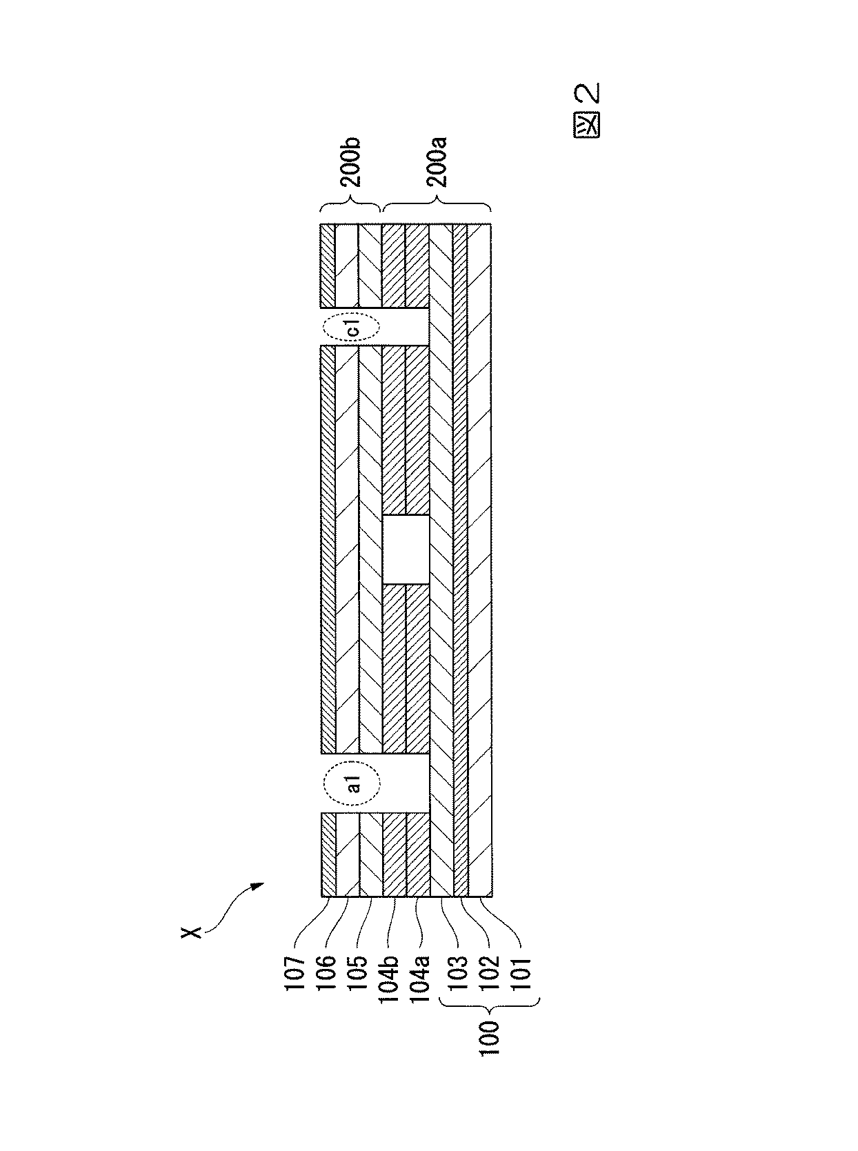
次いで、(1)で得られた第一の感光性接着剤を乾燥後の膜厚が15μmになる様に、フィルム厚み188μmのコスモシャインA4100(東洋紡社製、ポリエチレンテレフタレート基板101)(第一の基板)の易滑層102面(易接着処理面)に塗布し、3Dプリント用基板100を得た(図2参照。)。
(2) Preparation of 3D Printing Substrate Next, Cosmoshine A4100 (manufactured by Toyobo Co., Ltd.) having a film thickness of 188 μm so that the first photosensitive adhesive obtained in (1) has a film thickness of 15 μm after drying. A polyethylene terephthalate substrate 101) (first substrate) was applied to the easy-to-
2.細胞培養用流路の作製
(1)感光性造形材料の作製
以下の表2に示す原料を均一な溶液となるように十分に撹拌し、感光性造形材料を得た。
2. Preparation of cell culture flow path (1) Preparation of photosensitive modeling material The raw materials shown in Table 2 below were sufficiently stirred so as to form a uniform solution to obtain a photosensitive modeling material.
(2)細胞培養用流路の作製
次いで、(1)で得られた感光性造形材料を3Dプリント用基板100に1層厚みが20〜50μmとなる様にコーティングした後、デジタルマイクロミラーデバイス(DMD)により370μmを中心とする紫外線選択的に投影し、感光性造形材料を硬化させた。
さらに同様の方法で感光性造形材料を多層化し硬化させ、アセトンで3分間現像を行い、その後エアブローし微細な流路を有する構造体を得た。その後、高圧水銀灯により構造全体に紫外線を照射し、PGMEA、プロピレングリコールモノメチルエーテル、エタノールの順に洗浄を行い、乾燥し、細胞培養用流路200aを得た(図2参照。)。
(2) Preparation of Cell Culture Channel Next, the photosensitive modeling material obtained in (1) is coated on a
Further, the photosensitive modeling material was layered and cured by the same method, developed with acetone for 3 minutes, and then air blown to obtain a structure having a fine flow path. Then, the entire structure was irradiated with ultraviolet rays by a high-pressure mercury lamp, and PGMEA, propylene glycol monomethyl ether, and ethanol were washed in this order and dried to obtain a cell
3.細胞培養用流路天板の作製
(1)第一の接着剤の作製
以下の表3に示す原料を均一な溶液となるように十分に撹拌し、第一の接着剤を得た。
3. 3. Preparation of Channel Top Plate for Cell Culture (1) Preparation of First Adhesive The raw materials shown in Table 3 below were sufficiently stirred to obtain a uniform solution to obtain the first adhesive.
(2)細胞培養用流路天板の作製
次いで、(1)で得られた第一の接着剤を乾燥後の膜厚が20μmになる様に、フィルム厚み188μmのコスモシャインA4100(東洋紡社製、ポリエチレンテレフタレート基板106)(第二の基板)の未処理面に塗布し、このフィルムに炭酸ガスレーザを用いてインレットとなる穴(図2中のa1(3mm)及びc1(1.5mm))をあけ その後、エタノールに浸漬し乾燥し細胞培養用流路天板200bを得た(図2参照。)。
(2) Preparation of channel top plate for cell culture Next, Cosmoshine A4100 (manufactured by Toyobo Co., Ltd.) having a film thickness of 188 μm so that the first adhesive obtained in (1) has a film thickness of 20 μm after drying. , Polyethylene terephthalate substrate 106) (second substrate) is applied to the untreated surface, and holes (a1 (3 mm) and c1 (1.5 mm) in FIG. 2) to be inlets are formed in this film using a carbon dioxide gas laser. After opening, it was immersed in ethanol and dried to obtain a cell culture
4.細胞培養用チップの作製(細胞培養用流路天板の細胞培養用流路への貼り付け)
次いで、細胞培養用流路天板200bに仮止め剤として厚み50μmの両面テープを貼りつけ、穴(図2中のa1(3mm)及びc1(1.5mm))が細胞培養用流路200aの所定の位置に接着できるように顕微鏡を用いて位置合わせを行い、細胞培養用流路天板200bの第一の接着剤が塗布された面と細胞培養用流路200aとを仮止めした。その後80℃に加温されたラミネートロールに通し熱圧着を行い、中空構造を有する細胞培養用チップ1(X)を得た(図2参照。)。
4. Preparation of cell culture chips (pasting of cell culture flow path top plate to cell culture flow path)
Next, a double-sided tape having a thickness of 50 μm was attached to the cell culture flow path
[製造例2]細胞培養用チップ2の製造
上述の製造例1の「3.細胞培養用流路天板の作製」において、第一の接着剤の代わりに第二の接着剤を用いた以外は、製造例1と同様の方法を用いて、細胞培養用チップ2を製造した。第二の接着剤は、以下の表4に示す原料を均一な溶液となるように十分に撹拌し、第二の接着剤を得た。
[Production Example 2] Production of
[製造例3]細胞培養用チップ3の製造
上述の製造例1の「3.細胞培養用流路天板の作製」において、第一の接着剤の代わりに第三の接着剤を用いた以外は、製造例1と同様の方法を用いて、細胞培養用チップ2を製造した。第三の接着剤は、以下の表5に示す原料を均一な溶液となるように十分に撹拌し、第三の接着剤を得た。
[Production Example 3] Production of
[試験例1]細胞培養用チップ1を用いた細胞培養試験
1.細胞培養用チップ1と培養液貯留槽との接合
まず、細胞培養用チップを用いて細胞を培養するため、シリコーン樹脂(東レダウコーニング社製、SILPOT 184 W/C)製の培養液貯留槽を作製した。具体的には、PEEK製の切削加工によって製作した型にシリコーン樹脂のプレポリマーを注入し、減圧脱泡の後、70〜80℃で2時間加熱して培養液貯留槽を作製した。
次いで、製造例1で製造された細胞培養用チップ1の細胞培養用流路のインレット穴(a1およびc1)の位置に上記培養液貯留槽を接着剤(セメダイン株式会社製、セメダインスーパーX)により接合し、70〜80℃で2時間加熱した。次いで、20分程度、紫外線を照射し細胞培養用チップ1を滅菌した。培養液貯留槽を接合した細胞培養用チップ1を用いて、下記の方法に従って細胞培養試験を試みた。
[Test Example 1] Cell culture test using
Next, the culture solution storage tank was placed at the inlet holes (a1 and c1) of the cell culture flow path of the
2.細胞培養用流路の減圧脱法
培養液貯留槽にリン酸緩衝液(シグマアルドリッチ社製、ダルベッコリン酸緩衝生理食塩水)を入れ、チップ全体を減圧チャンバーに入れ、ダイヤフラムポンプ(DIVAC社製、DIVAC 0.6L)を用いて室温にて1時間減圧し、細胞培養用流路をリン酸緩衝液で満たした。
2. Decompression decompression method of cell culture flow path Put phosphate buffer (Sigma Aldrich, Dalbecolinic acid buffered saline) in the culture solution storage tank, put the entire chip in the decompression chamber, and diaphragm pump (DIVAC, DIVAC). The pressure was reduced to 1 hour at room temperature using 0.6 L), and the cell culture flow path was filled with a phosphate buffer solution.
3.細胞培養用流路のコーティング
次いで、培養液貯留槽内のリン酸緩衝液を吸引除去し、0.2mg/mL ファイブロネクチン溶液(シグマアルドリッチ社製、Fibronectin)約200μLを培養液貯留槽に添加した。次いで、培養液貯留槽を20kPaの圧力で4分間加圧することで細胞培養用流路内にファイブロネクチン溶液を導入した。圧力の調整はエアーポンプ(アズワン社製、ミニエアーポンプ EAP−01)とレギュレーター(ジーエルサイエンス社製、高性能調圧器 PR−4000)とを用いて行い、圧力計(コパル電子株式会社製、ハンディマノメーター PG−100 102GP)を用いて圧力を測定した。室温で1時間静置することで細胞培養用流路をファイブロネクチンでコーティングした。その後、培養液貯留槽内に残ったファイブロネクチン溶液を吸引除去した。次いで、培養液貯留槽に5%の血清(Thermofisher社製、HyClone Fetal Bovine Serum)及び1%の抗生物質(ナカライ社製、Penicillin−Streptomycin Solution)を含む培養液(Gibco社製、Dulbecco’s Modified Eagle Medium)を約200μL入れ、培養液貯留槽を20kPaの圧力で4分間加圧することで細胞培養用流路内の溶液を培養液に置換した。
3. 3. Coating of cell culture flow path Next, the phosphate buffer solution in the culture medium storage tank was removed by suction, and about 200 μL of 0.2 mg / mL fibronectin solution (Fibronectin, manufactured by Sigma-Aldrich) was added to the culture medium storage tank. .. Next, the fibronectin solution was introduced into the cell culture flow path by pressurizing the culture solution storage tank at a pressure of 20 kPa for 4 minutes. The pressure is adjusted using an air pump (Azuwan, mini air pump EAP-01) and a regulator (GL Sciences, high-performance pressure regulator PR-4000), and a pressure gauge (Copal Electronics Co., Ltd., Handy). The pressure was measured using a manometer (PG-100 102GP). The cell culture channel was coated with fibronectin by allowing to stand at room temperature for 1 hour. Then, the fibronectin solution remaining in the culture solution storage tank was removed by suction. Next, a culture medium (Gibco's Dulvecco About 200 μL of Eagle's Medium) was added, and the culture solution storage tank was pressurized at a pressure of 20 kPa for 4 minutes to replace the solution in the cell culture flow path with the culture solution.
4.細胞導入及び静置培養
理化学研究所より分譲されたNIH3T3細胞を培養液で培養し、0.25%トリプシン−EDTA溶液(Thermofisher社製)を用いて回収した。回収した細胞を5×10⁵cells/mLの濃度となるように培養液で懸濁させた。次いで、細胞懸濁約200μLを培養液貯留槽に添加し、顕微鏡観察下で培養液貯留槽を20kPaの圧力で加圧して細胞懸濁液を細胞培養用流路に導入し、細胞が細胞培養用流路に導入されたことを確認した。培養液貯留槽に残った細胞懸濁液を吸引除去した後に、培養液貯留槽に培養液を添加し、5%二酸化炭素を含む空気の飽和水蒸気圧下において37℃で静置し、細胞の接着を促した。
4. Cell introduction and static culture NIH3T3 cells distributed by RIKEN were cultured in a culture medium and recovered using a 0.25% trypsin-EDTA solution (manufactured by Thermofiser). The recovered cells were suspended in culture medium to a concentration of 5 × 10 5 cells / mL. Next, about 200 μL of cell suspension was added to the culture medium storage tank, and the culture solution storage tank was pressurized at a pressure of 20 kPa under microscopic observation to introduce the cell suspension into the cell culture flow path, and the cells were cultured. It was confirmed that it was introduced into the flow path. After removing the cell suspension remaining in the culture solution storage tank by suction, the culture solution is added to the culture solution storage tank, and the cells are allowed to stand at 37 ° C. under saturated steam pressure of air containing 5% carbon dioxide to adhere cells. Prompted.
5.灌流培養
約6時間の静置培養を経て細胞が細胞培養用流路に接着していることを確認した後、培養液貯留槽に培養液を500μL添加した。培養液の入った培養液貯留槽に対して5kPaで4分間の加圧と大気圧解放176分間の間欠的な加圧とを繰り返すことで、灌流培養を行った。1日に1回、培養液貯留槽内の培養液を新鮮な培養液に交換した。この際に、培養液貯留槽に残存する培養液の重さを測定することで灌流培養中の培地流量を測定した。灌流培養は細胞導入後3日目まで継続した。また、培養中には適宜、細胞の様子を、倒立型蛍光顕微鏡(オリンパス社製、IX71)を用いて観察し、位相差顕微鏡画像を撮影した。
5. Perfusion culture After confirming that the cells adhered to the cell culture flow path after static culture for about 6 hours, 500 μL of the culture solution was added to the culture solution storage tank. Perfusion culture was performed by repeating pressurization at 5 kPa for 4 minutes and intermittent pressurization for 176 minutes at atmospheric pressure release to the culture solution storage tank containing the culture solution. Once a day, the culture broth in the culture broth storage tank was replaced with a fresh culture broth. At this time, the flow rate of the medium during the perfusion culture was measured by measuring the weight of the culture solution remaining in the culture solution storage tank. Perfusion culture continued until
6.Live/Dead染色
灌流培養を3日間行った後、細胞培養用流路内の細胞の生死を確認するため、Live/Dead染色試薬(Life Technologies社製、LIVE/DEAD(登録商標)Viability/Cytotoxicity Kit, for mammalian cells)を用いて、細胞培養用流路内の細胞を染色した。Live/Dead染色は以下のプロトコルに従って行った。リン酸緩衝液4mLにLive/Dead染色試薬に含まれるCalcein AM溶液4μL、Ethidium homodimer−1溶液16μLを添加し混合し、Live/Dead染色液を調製した。培養液貯留槽にリン酸緩衝液を約200μL入れ、培養液貯留槽を20kPaの圧力で4分間加圧することで細胞培養用流路内を洗浄した。その後、培養液貯留槽にLive/Dead染色液を約200μL添加し、培養液貯留槽を20kPaの圧力で4分間加圧することで細胞培養用流路内にLive/Dead染色液を導入し、遮光して室温下で30分程度染色した。その後、倒立型蛍光顕微鏡(オリンパス社製、IX71)を用いて蛍光顕微鏡画像IX71位相差顕微鏡画像を撮影した。蛍光画像はFITC(緑色蛍光:蛍光波長488nm、励起波長530nm)及びTexasRed(赤色蛍光:蛍光波長590nm、励起波長615nm)に適合する蛍光フィルター(Chroma社製、マルチバンドフィルター(ET−DAPI/FITC/TexasRed))を用いて撮像した。
6. Live / Dead Staining After perfusion culture for 3 days, Live / Dead Staining Reagent (Live Technology / Cytotoxicity Kit, manufactured by Life Technologies, Inc.) to confirm the life and death of cells in the cell culture flow path. , For mammal cells) were used to stain the cells in the cell culture channel. Live / Dead staining was performed according to the following protocol. 4 μL of Calcein AM solution and 16 μL of Ethidium homodimer-1 solution contained in the Live / Dead stain reagent were added to 4 mL of phosphate buffer and mixed to prepare a Live / Dead stain. Approximately 200 μL of phosphate buffer was placed in the culture solution storage tank, and the inside of the cell culture flow path was washed by pressurizing the culture solution storage tank at a pressure of 20 kPa for 4 minutes. After that, about 200 μL of Live / Dead staining solution was added to the culture solution storage tank, and the culture solution storage tank was pressurized at a pressure of 20 kPa for 4 minutes to introduce the Live / Dead staining solution into the cell culture flow path and shield it from light. Then, the cells were stained at room temperature for about 30 minutes. Then, a fluorescence microscope image IX71 phase-contrast microscope image was taken using an inverted fluorescence microscope (IX71 manufactured by Olympus Corporation). The fluorescence image is a fluorescence filter (Chroma, multi-band filter (ET-DAPI / FITC /) compatible with FITC (green fluorescence: fluorescence wavelength 488 nm, excitation wavelength 530 nm) and TexasRed (red fluorescence: fluorescence wavelength 590 nm, excitation wavelength 615 nm). Imaging was performed using TexasRed)).
7.結果
上記の方法に従ってNIH3T3細胞を培養し、位相差顕微鏡により観察したところ、細胞導入1日後には細胞が接着して伸展している様子が観察され、3日間の灌流培養をとおして細胞が増殖する様子が観察された。同様の細胞培養用チップ1を2枚追加で作製して同様の試験を行ったが、細胞の接着、伸展、及び増殖性に差はなく再現性よく細胞を培養できることが確認された。
7. Results When NIH3T3 cells were cultured according to the above method and observed with a phase-contrast microscope, it was observed that the cells adhered and expanded 1 day after the introduction of the cells, and the cells proliferated through the perfusion culture for 3 days. It was observed that the cells were doing. Two similar
また、37℃における3日間の灌流培養の際の培養液の流量は安定していた。培養液の流量に関する再現性を確認するため、4本の細胞培養用流路が形成された細胞培養用チップ1を2枚作製し、合計8本の細胞培養用流路で3日間、毎日培養液の流量を測定した。8本の細胞培養用流路の3日間の流量の測定値は274±26μL/day(平均値±標準偏差)となっており、細胞培養用流路毎の差も少なく、経時的にも安定であることが確認された。
また、灌流培養後のLive/Dead染色においては、細胞培養流路内のほぼ全て(95%以上)の細胞がCalceinで染色される生細胞であることが確認され、高い生存率を保って培養できることが確認された。また、少数(5%以下)の細胞がEthidium homodimer−1に染色される死細胞であることも確認された。このことにより、製造例1で製造された細胞培養用チップ1の細胞培養用流路内の細胞を染色した場合に、緑色蛍光及び赤色蛍光で観察可能であることが確認された。
In addition, the flow rate of the culture solution during perfusion culture at 37 ° C. for 3 days was stable. In order to confirm the reproducibility of the flow rate of the culture solution, two
In Live / Dead staining after perfusion culture, it was confirmed that almost all cells (95% or more) in the cell culture channel were live cells stained with Calcein, and the cells were cultured while maintaining a high survival rate. It was confirmed that it could be done. It was also confirmed that a small number (5% or less) of cells were dead cells stained with Ethidium homodimer-1. From this, it was confirmed that when the cells in the cell culture flow path of the
以上の試験により、製造例1で製造された細胞培養用チップ1を用いて、37℃で培養液を灌流して細胞培養が可能であり、灌流培養によって細胞が増殖し、増殖した細胞が高い生存率を保っていることが確認された。また、製造例1で製造された細胞培養用チップ1では、灌流培養の間、培養液流量が安定していることが確認され、細胞の明視野及び蛍光観察(緑色蛍光及び赤色蛍光)が可能であることが確認された。
According to the above test, the
[試験例2]細胞培養用チップ2を用いた細胞培養試験
製造例2で製造された細胞培養用チップ2を用いた以外は、試験例1に示す方法と同様の方法を用いて、培養液貯留槽を接合し、培養液貯留槽を接合した細胞培養用チップ2を用いて、試験例1に示す方法と同様の方法を用いて、細胞培養試験を試みた。
試験例1と同様の試験を行った結果、製造例2で製造された細胞培養用チップ2では、灌流培養の間、培養液流量が安定していることが確認され、細胞の明視野及び蛍光観察(緑色蛍光及び赤色蛍光)が可能であることが確認された。
[Test Example 2] Cell culture test using cell culture chip 2 A culture solution is used in the same manner as in Test Example 1 except that the
As a result of conducting the same test as in Test Example 1, it was confirmed that the
[試験例3]細胞培養用チップ3を用いた細胞培養試験
製造例3で製造された細胞培養用チップ3を用いた以外は、試験例1に示す方法と同様の方法を用いて、培養液貯留槽を接合し、培養液貯留槽を接合した細胞培養用チップ3を用いて、試験例1に示す方法と同様の方法を用いて、細胞培養試験を試みた。
[Test Example 3] Cell culture test using cell culture chip 3 A culture solution is used in the same manner as in Test Example 1 except that the
試験例1と同様の試験を行った結果、細胞培養用チップ3では、37℃で6時間の静置培養を行っている間に、細胞培養用流路天板に塗布された第三の接着剤が変形し、流路が完全に閉塞してしまった。培養液を灌流するために培養液貯留槽に培地を導入して加圧したが、流路が閉塞しているため培養液を灌流することができなかった。その後、培養液灌流のための加圧を2日間継続し、観察を続けたが、流路閉塞が原因で培養液を灌流することができず、細胞培養用流路に導入された細胞の状態が悪化する様子が観察された。また、流路が閉塞しているため、Live/Dead染色を行うことはできなかった。
以上の試験により、製造例3で製造された細胞培養用チップ3では、37℃で培養液を灌流して細胞培養を行うことが不可能であることが確認された。
As a result of conducting the same test as in Test Example 1, in the
From the above test, it was confirmed that the
本発明によれば、微細な流路構造を備えた細胞培養用チップを低コストで大量に生産することができる。 According to the present invention, a cell culture chip having a fine channel structure can be mass-produced at low cost.
1A…細胞培養用チップ、1…第一の基板、2…感光性接着剤層、3a…第一の感光性造形材層、3b…第二の感光性造形材層、3’…液状の感光性造形材料、4…作業テーブル、5a…第一の槽、5b…第二の槽、6…レーザ照射器、7…ミラー、8…紫外線、9…現像液、10…3Dプリント用基板、11…第二の基板、12…第一の接着剤層、20a…細胞培養用流路、20b…細胞培養用流路天板、100…3Dプリント用基板、101…PET基板(第一の基板)、102,107…易滑層、103…第一の感光性接着剤層、104a…第一の感光性造形材層、104b…第二の感光性造形材層、105…第一の接着剤層、106…PET基板(第二の基板)、200a…細胞培養用流路、200b…細胞培養用流路天板、X…細胞培養用チップ1。
1A ... Cell culture chip, 1 ... First substrate, 2 ... Photosensitive adhesive layer, 3a ... First photosensitive molding material layer, 3b ... Second photosensitive molding material layer, 3'... Liquid photosensitive Sex modeling material, 4 ... work table, 5a ... first tank, 5b ... second tank, 6 ... laser irradiator, 7 ... mirror, 8 ... ultraviolet rays, 9 ... developing liquid, 10 ... 3D printing substrate, 11 ... second substrate, 12 ... first adhesive layer, 20a ... cell culture flow path, 20b ... cell culture flow path top plate, 100 ... 3D printing substrate, 101 ... PET substrate (first substrate) , 102, 107 ... Easy-to-slip layer, 103 ... First photosensitive adhesive layer, 104a ... First photosensitive molding material layer, 104b ... Second photosensitive molding material layer, 105 ... First adhesive layer , 106 ... PET substrate (second substrate), 200a ... Cell culture flow path, 200b ... Cell culture flow path top plate, X ...
Claims (4)
前記3Dプリント用基板上に、感光性造形材料を製膜してなる感光性造形材層に、紫外線を選択的に照射し、前記感光性造形材層を選択的に硬化させる工程Bと、
選択的に硬化した感光性造形材層上に、更に感光性造形材料を製膜して感光性造形材層を重層し、重層された感光性造形材層に紫外線を選択的に照射し、前記重層された感光性造形材層を選択的に硬化させる工程Cと、
前記工程Cを複数回繰り返した後、未硬化部分を現像し細胞培養用流路を得る工程Dと、
透明性を有する第二の基板上に、第一の接着剤を製膜して第一の接着剤層を形成させ、細胞培養用流路天板を得る工程Eと、
前記細胞培養用流路と前記細胞培養用流路天板とを、前記第一の接着剤層を介して接合し、熱圧着させて中空構造を有するマイクロ流路構造体を得る工程Fと、を有し、
前記第一の接着剤が、Tgが5℃以上のポリエステル系樹脂であり、熱で圧着される接着剤であることを特徴とする細胞培養用チップの製造方法。 Step A of applying a photosensitive adhesive on the first transparent substrate to form a photosensitive adhesive layer to obtain a substrate for 3D printing.
Step B of selectively irradiating the photosensitive modeling material layer formed by forming a film of the photosensitive modeling material on the 3D printing substrate with ultraviolet rays to selectively cure the photosensitive modeling material layer.
A photosensitive modeling material is further formed on the selectively cured photosensitive modeling material layer to superimpose the photosensitive modeling material layer, and the layered photosensitive modeling material layer is selectively irradiated with ultraviolet rays. Step C, which selectively cures the layered photosensitive molding material layer,
After repeating the above step C a plurality of times, the uncured portion is developed to obtain a cell culture flow path, and the step D
Step E of forming a film of the first adhesive on the second transparent substrate to form the first adhesive layer to obtain a flow path top plate for cell culture.
Step F of joining the cell culture flow path and the cell culture flow path top plate via the first adhesive layer and thermocompression bonding to obtain a microchannel structure having a hollow structure. Have,
Wherein the first adhesive, Tg is Ri polyester resin der above 5 ° C., a manufacturing method of a cell culture chip, characterized in that an adhesive which is crimped by heat.
Priority Applications (3)
| Application Number | Priority Date | Filing Date | Title |
|---|---|---|---|
| JP2016253304A JP6861408B2 (en) | 2016-12-27 | 2016-12-27 | Method for manufacturing cell culture chips |
| US15/824,081 US10941376B2 (en) | 2016-12-27 | 2017-11-28 | Method for producing chip for cell culture |
| EP17209880.8A EP3342852A3 (en) | 2016-12-27 | 2017-12-21 | Method for producing chip for cell culture |
Applications Claiming Priority (1)
| Application Number | Priority Date | Filing Date | Title |
|---|---|---|---|
| JP2016253304A JP6861408B2 (en) | 2016-12-27 | 2016-12-27 | Method for manufacturing cell culture chips |
Publications (2)
| Publication Number | Publication Date |
|---|---|
| JP2018102236A JP2018102236A (en) | 2018-07-05 |
| JP6861408B2 true JP6861408B2 (en) | 2021-04-21 |
Family
ID=60954785
Family Applications (1)
| Application Number | Title | Priority Date | Filing Date |
|---|---|---|---|
| JP2016253304A Active JP6861408B2 (en) | 2016-12-27 | 2016-12-27 | Method for manufacturing cell culture chips |
Country Status (3)
| Country | Link |
|---|---|
| US (1) | US10941376B2 (en) |
| EP (1) | EP3342852A3 (en) |
| JP (1) | JP6861408B2 (en) |
Families Citing this family (7)
| Publication number | Priority date | Publication date | Assignee | Title |
|---|---|---|---|---|
| US11760966B2 (en) | 2019-06-14 | 2023-09-19 | University Of Connecticut | Multigel tumor-on-a-chip system |
| JP7433059B2 (en) | 2020-01-22 | 2024-02-19 | 東京応化工業株式会社 | Manufacturing method for cell culture chips |
| EP4366873A4 (en) * | 2021-07-08 | 2025-08-06 | Ourotech Inc | SYSTEMS AND METHODS FOR PREDICTING TREATMENT EFFECTIVENESS |
| KR102506168B1 (en) * | 2021-07-20 | 2023-03-08 | 한국생산기술연구원 | A assembly type transmission efficiency evaluation chip, assembly type transmission efficiency evaluation system, and control method thereof |
| WO2023027145A1 (en) | 2021-08-26 | 2023-03-02 | 東京応化工業株式会社 | Cell culture chip, cell culture device, method for producing cell culture chip, and method for culturing cells |
| EP4394026A1 (en) | 2021-08-26 | 2024-07-03 | Tokyo Ohka Kogyo Co., Ltd. | Chip for cell culturing, device for cell culturing, method for manufacturing chip for cell culturing, and method for culturing cells |
| CN115625892A (en) * | 2022-10-20 | 2023-01-20 | 广州黑格智造信息科技有限公司 | Forming platform of 3D printing equipment and preparation method thereof |
Family Cites Families (19)
| Publication number | Priority date | Publication date | Assignee | Title |
|---|---|---|---|---|
| JPS6238408A (en) * | 1985-08-13 | 1987-02-19 | Fuji Photo Film Co Ltd | Cover film for microscope |
| WO2001017797A1 (en) * | 1999-09-10 | 2001-03-15 | Caliper Technologies Corp. | Microfabrication methods and devices |
| US20070037277A1 (en) | 2001-04-25 | 2007-02-15 | Michael Shuler | Pharmacokinetic-based culture system with biological barriers |
| JP4327616B2 (en) * | 2004-01-26 | 2009-09-09 | 旭化成イーマテリアルズ株式会社 | Photosensitive coating resin composition |
| EP1729884A1 (en) | 2004-01-30 | 2006-12-13 | Corning Incorporated | Multiwell plate and method for making multiwell plate using a low cytotoxicity photocurable adhesive |
| JP2007031602A (en) * | 2005-07-28 | 2007-02-08 | Mitsubishi Plastics Ind Ltd | Laminated film with adhesive for electrical materials |
| WO2009042671A1 (en) * | 2007-09-24 | 2009-04-02 | The Board Of Trustees Of The University Of Illinois | Three-dimensional microfabricated bioreactors with embedded capillary network |
| JP5114362B2 (en) | 2008-10-30 | 2013-01-09 | 独立行政法人科学技術振興機構 | 3D object made by stereolithography and cell-adapted |
| JP2010112730A (en) | 2008-11-04 | 2010-05-20 | Fujifilm Corp | Detecting method using flow passage type sensor chip, flow passage type sensor chip and manufacturing method for the same |
| WO2010107497A2 (en) * | 2009-03-18 | 2010-09-23 | The Regents Of The University Of California | Honeycomb shrink wells for stem cell culture |
| WO2011089892A1 (en) * | 2010-01-19 | 2011-07-28 | 国立大学法人東京工業大学 | Method for bonding hardened silicone resin, method for joining substrate having fine structure, and method for manufacturing micro fluid device using the method for joining. |
| US8206664B2 (en) * | 2010-07-06 | 2012-06-26 | Xerox Corporation | Methods of producing multi-layered microfluidic devices |
| JP2013164311A (en) * | 2012-02-10 | 2013-08-22 | Enplas Corp | Fluid handing device and manufacturing method therefor |
| US9168697B2 (en) * | 2012-08-16 | 2015-10-27 | Stratasys, Inc. | Additive manufacturing system with extended printing volume, and methods of use thereof |
| JP6265508B2 (en) | 2012-09-21 | 2018-01-24 | マサチューセッツ インスティテュート オブ テクノロジー | Microfluidic device and use thereof |
| JP5986482B2 (en) * | 2012-11-05 | 2016-09-06 | 株式会社神戸製鋼所 | Thermal insulation member |
| EP3007882B1 (en) | 2013-06-13 | 2019-11-20 | Aspect Biosystems Ltd. | System for additive manufacturing of three-dimensional structures and method for same |
| JP6357006B2 (en) | 2014-04-18 | 2018-07-11 | 東京応化工業株式会社 | Photosensitive resin composition for forming cell culture substrate |
| WO2016164861A1 (en) | 2015-04-10 | 2016-10-13 | The Regents Of The University Of California | Microfluidic assisted perfusion devices |
-
2016
- 2016-12-27 JP JP2016253304A patent/JP6861408B2/en active Active
-
2017
- 2017-11-28 US US15/824,081 patent/US10941376B2/en active Active
- 2017-12-21 EP EP17209880.8A patent/EP3342852A3/en active Pending
Also Published As
| Publication number | Publication date |
|---|---|
| JP2018102236A (en) | 2018-07-05 |
| EP3342852A2 (en) | 2018-07-04 |
| US20180179481A1 (en) | 2018-06-28 |
| EP3342852A3 (en) | 2018-07-11 |
| US10941376B2 (en) | 2021-03-09 |
Similar Documents
| Publication | Publication Date | Title |
|---|---|---|
| JP6861408B2 (en) | Method for manufacturing cell culture chips | |
| US9346214B2 (en) | Film-forming composition for optical imprint and method for producing optical member | |
| JP7433059B2 (en) | Manufacturing method for cell culture chips | |
| KR100929381B1 (en) | Mold sheet composition and mold sheet manufacturing method using the same | |
| US9690193B2 (en) | Curable composition for nanoimprinting and cured product | |
| CN101925840B (en) | Resin composition for clad formation, resin film for clad formation using same, optical waveguide and optical module using same | |
| JP4466794B2 (en) | Photosensitive resin composition, photosensitive resin cured product, photosensitive resin film, photosensitive resin film cured product, and optical waveguide obtained using these | |
| CN107922522A (en) | Composite material, photosensitive resin composition for solder resist, and photosensitive element | |
| TW200813629A (en) | Photosensitive resin composition for optical waveguide, dry film, optical waveguide, and process for producing the same | |
| CN102159976B (en) | Optical waveguide | |
| CN114341280B (en) | Building materials for 3D printing | |
| JP5624908B2 (en) | Adhesive composition | |
| CN102597129A (en) | Photocurable coating composition and coating film formed by hardening same | |
| JP5387370B2 (en) | Optical waveguide forming resin composition, optical waveguide forming resin film using the same, and optical waveguide using the same | |
| US10336976B2 (en) | Photosensitive resin composition for forming cell culture substrate | |
| JP2010091733A (en) | Resin composition for forming core part and resin film for forming core part using the same, and optical waveguide using these | |
| JP2014076557A (en) | Method for producing article having fine rugged structure, and method for producing replica mold having fine rugged structure | |
| JP2003047908A (en) | Method for forming stain-resistant cured film on substrate surface, substrate coated with the film, method for preventing contamination of substrate | |
| JP2010091734A (en) | Resin composition for forming core part and resin film for forming core part using the same, and optical waveguide using these | |
| CN101855579A (en) | Resin composition for optical waveguide and optical waveguide | |
| TWI708808B (en) | Active energy ray curable resin composition, cured product and optical sheet for optical articles | |
| JP2010046948A (en) | Resin laminate and method of manufacturing resin laminate | |
| KR101114475B1 (en) | Photosensitive resin composition comprising negative photosensitive copolymer with high heat resistance and Insulating film for liquid crystal display prepared by the same | |
| Tak et al. | Surface energy-tunable iso decyl acrylate based molds for low pressure-nanoimprint lithography |
Legal Events
| Date | Code | Title | Description |
|---|---|---|---|
| A621 | Written request for application examination |
Free format text: JAPANESE INTERMEDIATE CODE: A621 Effective date: 20190917 |
|
| A977 | Report on retrieval |
Free format text: JAPANESE INTERMEDIATE CODE: A971007 Effective date: 20200720 |
|
| A131 | Notification of reasons for refusal |
Free format text: JAPANESE INTERMEDIATE CODE: A131 Effective date: 20200811 |
|
| A521 | Request for written amendment filed |
Free format text: JAPANESE INTERMEDIATE CODE: A523 Effective date: 20200923 |
|
| TRDD | Decision of grant or rejection written | ||
| A01 | Written decision to grant a patent or to grant a registration (utility model) |
Free format text: JAPANESE INTERMEDIATE CODE: A01 Effective date: 20210222 |
|
| A61 | First payment of annual fees (during grant procedure) |
Free format text: JAPANESE INTERMEDIATE CODE: A61 Effective date: 20210322 |
|
| R150 | Certificate of patent or registration of utility model |
Ref document number: 6861408 Country of ref document: JP Free format text: JAPANESE INTERMEDIATE CODE: R150 |
|
| R250 | Receipt of annual fees |
Free format text: JAPANESE INTERMEDIATE CODE: R250 |
|
| R250 | Receipt of annual fees |
Free format text: JAPANESE INTERMEDIATE CODE: R250 |
|
| R250 | Receipt of annual fees |
Free format text: JAPANESE INTERMEDIATE CODE: R250 |