JP6854882B2 - Liquid crystal display panel and liquid crystal display device - Google Patents
Liquid crystal display panel and liquid crystal display device Download PDFInfo
- Publication number
- JP6854882B2 JP6854882B2 JP2019509477A JP2019509477A JP6854882B2 JP 6854882 B2 JP6854882 B2 JP 6854882B2 JP 2019509477 A JP2019509477 A JP 2019509477A JP 2019509477 A JP2019509477 A JP 2019509477A JP 6854882 B2 JP6854882 B2 JP 6854882B2
- Authority
- JP
- Japan
- Prior art keywords
- substrate
- layer
- liquid crystal
- crystal display
- array substrate
- Prior art date
- Legal status (The legal status is an assumption and is not a legal conclusion. Google has not performed a legal analysis and makes no representation as to the accuracy of the status listed.)
- Active
Links
- 239000004973 liquid crystal related substance Substances 0.000 title claims description 62
- 239000000758 substrate Substances 0.000 claims description 169
- 239000010410 layer Substances 0.000 claims description 136
- 239000010408 film Substances 0.000 claims description 45
- 125000006850 spacer group Chemical group 0.000 claims description 35
- 239000010409 thin film Substances 0.000 claims description 19
- 238000002161 passivation Methods 0.000 claims description 18
- 239000011241 protective layer Substances 0.000 claims description 18
- 238000011161 development Methods 0.000 claims description 15
- 230000018109 developmental process Effects 0.000 claims description 15
- 239000011159 matrix material Substances 0.000 claims description 12
- 238000000926 separation method Methods 0.000 claims description 9
- 229920002120 photoresistant polymer Polymers 0.000 description 9
- 210000002858 crystal cell Anatomy 0.000 description 6
- 238000005516 engineering process Methods 0.000 description 3
- 238000000034 method Methods 0.000 description 3
- 230000002093 peripheral effect Effects 0.000 description 3
- 230000015572 biosynthetic process Effects 0.000 description 2
- 238000002955 isolation Methods 0.000 description 2
- 230000009286 beneficial effect Effects 0.000 description 1
- 230000007423 decrease Effects 0.000 description 1
- 238000010586 diagram Methods 0.000 description 1
- 238000006073 displacement reaction Methods 0.000 description 1
- 239000011521 glass Substances 0.000 description 1
- 238000010030 laminating Methods 0.000 description 1
- 238000004519 manufacturing process Methods 0.000 description 1
- 238000012986 modification Methods 0.000 description 1
- 230000004048 modification Effects 0.000 description 1
- 238000007789 sealing Methods 0.000 description 1
Images


Classifications
-
- G—PHYSICS
- G02—OPTICS
- G02F—OPTICAL DEVICES OR ARRANGEMENTS FOR THE CONTROL OF LIGHT BY MODIFICATION OF THE OPTICAL PROPERTIES OF THE MEDIA OF THE ELEMENTS INVOLVED THEREIN; NON-LINEAR OPTICS; FREQUENCY-CHANGING OF LIGHT; OPTICAL LOGIC ELEMENTS; OPTICAL ANALOGUE/DIGITAL CONVERTERS
- G02F1/00—Devices or arrangements for the control of the intensity, colour, phase, polarisation or direction of light arriving from an independent light source, e.g. switching, gating or modulating; Non-linear optics
- G02F1/01—Devices or arrangements for the control of the intensity, colour, phase, polarisation or direction of light arriving from an independent light source, e.g. switching, gating or modulating; Non-linear optics for the control of the intensity, phase, polarisation or colour
- G02F1/13—Devices or arrangements for the control of the intensity, colour, phase, polarisation or direction of light arriving from an independent light source, e.g. switching, gating or modulating; Non-linear optics for the control of the intensity, phase, polarisation or colour based on liquid crystals, e.g. single liquid crystal display cells
- G02F1/133—Constructional arrangements; Operation of liquid crystal cells; Circuit arrangements
- G02F1/1333—Constructional arrangements; Manufacturing methods
- G02F1/1335—Structural association of cells with optical devices, e.g. polarisers or reflectors
- G02F1/133509—Filters, e.g. light shielding masks
- G02F1/133514—Colour filters
-
- G—PHYSICS
- G02—OPTICS
- G02F—OPTICAL DEVICES OR ARRANGEMENTS FOR THE CONTROL OF LIGHT BY MODIFICATION OF THE OPTICAL PROPERTIES OF THE MEDIA OF THE ELEMENTS INVOLVED THEREIN; NON-LINEAR OPTICS; FREQUENCY-CHANGING OF LIGHT; OPTICAL LOGIC ELEMENTS; OPTICAL ANALOGUE/DIGITAL CONVERTERS
- G02F1/00—Devices or arrangements for the control of the intensity, colour, phase, polarisation or direction of light arriving from an independent light source, e.g. switching, gating or modulating; Non-linear optics
- G02F1/01—Devices or arrangements for the control of the intensity, colour, phase, polarisation or direction of light arriving from an independent light source, e.g. switching, gating or modulating; Non-linear optics for the control of the intensity, phase, polarisation or colour
- G02F1/13—Devices or arrangements for the control of the intensity, colour, phase, polarisation or direction of light arriving from an independent light source, e.g. switching, gating or modulating; Non-linear optics for the control of the intensity, phase, polarisation or colour based on liquid crystals, e.g. single liquid crystal display cells
- G02F1/133—Constructional arrangements; Operation of liquid crystal cells; Circuit arrangements
- G02F1/1333—Constructional arrangements; Manufacturing methods
- G02F1/1339—Gaskets; Spacers; Sealing of cells
- G02F1/13394—Gaskets; Spacers; Sealing of cells spacers regularly patterned on the cell subtrate, e.g. walls, pillars
-
- G—PHYSICS
- G02—OPTICS
- G02F—OPTICAL DEVICES OR ARRANGEMENTS FOR THE CONTROL OF LIGHT BY MODIFICATION OF THE OPTICAL PROPERTIES OF THE MEDIA OF THE ELEMENTS INVOLVED THEREIN; NON-LINEAR OPTICS; FREQUENCY-CHANGING OF LIGHT; OPTICAL LOGIC ELEMENTS; OPTICAL ANALOGUE/DIGITAL CONVERTERS
- G02F1/00—Devices or arrangements for the control of the intensity, colour, phase, polarisation or direction of light arriving from an independent light source, e.g. switching, gating or modulating; Non-linear optics
- G02F1/01—Devices or arrangements for the control of the intensity, colour, phase, polarisation or direction of light arriving from an independent light source, e.g. switching, gating or modulating; Non-linear optics for the control of the intensity, phase, polarisation or colour
- G02F1/13—Devices or arrangements for the control of the intensity, colour, phase, polarisation or direction of light arriving from an independent light source, e.g. switching, gating or modulating; Non-linear optics for the control of the intensity, phase, polarisation or colour based on liquid crystals, e.g. single liquid crystal display cells
- G02F1/133—Constructional arrangements; Operation of liquid crystal cells; Circuit arrangements
- G02F1/1333—Constructional arrangements; Manufacturing methods
- G02F1/13338—Input devices, e.g. touch panels
-
- G—PHYSICS
- G02—OPTICS
- G02F—OPTICAL DEVICES OR ARRANGEMENTS FOR THE CONTROL OF LIGHT BY MODIFICATION OF THE OPTICAL PROPERTIES OF THE MEDIA OF THE ELEMENTS INVOLVED THEREIN; NON-LINEAR OPTICS; FREQUENCY-CHANGING OF LIGHT; OPTICAL LOGIC ELEMENTS; OPTICAL ANALOGUE/DIGITAL CONVERTERS
- G02F1/00—Devices or arrangements for the control of the intensity, colour, phase, polarisation or direction of light arriving from an independent light source, e.g. switching, gating or modulating; Non-linear optics
- G02F1/01—Devices or arrangements for the control of the intensity, colour, phase, polarisation or direction of light arriving from an independent light source, e.g. switching, gating or modulating; Non-linear optics for the control of the intensity, phase, polarisation or colour
- G02F1/13—Devices or arrangements for the control of the intensity, colour, phase, polarisation or direction of light arriving from an independent light source, e.g. switching, gating or modulating; Non-linear optics for the control of the intensity, phase, polarisation or colour based on liquid crystals, e.g. single liquid crystal display cells
- G02F1/133—Constructional arrangements; Operation of liquid crystal cells; Circuit arrangements
- G02F1/1333—Constructional arrangements; Manufacturing methods
- G02F1/1335—Structural association of cells with optical devices, e.g. polarisers or reflectors
- G02F1/133509—Filters, e.g. light shielding masks
- G02F1/133512—Light shielding layers, e.g. black matrix
-
- G—PHYSICS
- G02—OPTICS
- G02F—OPTICAL DEVICES OR ARRANGEMENTS FOR THE CONTROL OF LIGHT BY MODIFICATION OF THE OPTICAL PROPERTIES OF THE MEDIA OF THE ELEMENTS INVOLVED THEREIN; NON-LINEAR OPTICS; FREQUENCY-CHANGING OF LIGHT; OPTICAL LOGIC ELEMENTS; OPTICAL ANALOGUE/DIGITAL CONVERTERS
- G02F1/00—Devices or arrangements for the control of the intensity, colour, phase, polarisation or direction of light arriving from an independent light source, e.g. switching, gating or modulating; Non-linear optics
- G02F1/01—Devices or arrangements for the control of the intensity, colour, phase, polarisation or direction of light arriving from an independent light source, e.g. switching, gating or modulating; Non-linear optics for the control of the intensity, phase, polarisation or colour
- G02F1/13—Devices or arrangements for the control of the intensity, colour, phase, polarisation or direction of light arriving from an independent light source, e.g. switching, gating or modulating; Non-linear optics for the control of the intensity, phase, polarisation or colour based on liquid crystals, e.g. single liquid crystal display cells
- G02F1/133—Constructional arrangements; Operation of liquid crystal cells; Circuit arrangements
- G02F1/1333—Constructional arrangements; Manufacturing methods
- G02F1/1335—Structural association of cells with optical devices, e.g. polarisers or reflectors
- G02F1/133509—Filters, e.g. light shielding masks
- G02F1/133514—Colour filters
- G02F1/133516—Methods for their manufacture, e.g. printing, electro-deposition or photolithography
-
- G—PHYSICS
- G02—OPTICS
- G02F—OPTICAL DEVICES OR ARRANGEMENTS FOR THE CONTROL OF LIGHT BY MODIFICATION OF THE OPTICAL PROPERTIES OF THE MEDIA OF THE ELEMENTS INVOLVED THEREIN; NON-LINEAR OPTICS; FREQUENCY-CHANGING OF LIGHT; OPTICAL LOGIC ELEMENTS; OPTICAL ANALOGUE/DIGITAL CONVERTERS
- G02F1/00—Devices or arrangements for the control of the intensity, colour, phase, polarisation or direction of light arriving from an independent light source, e.g. switching, gating or modulating; Non-linear optics
- G02F1/01—Devices or arrangements for the control of the intensity, colour, phase, polarisation or direction of light arriving from an independent light source, e.g. switching, gating or modulating; Non-linear optics for the control of the intensity, phase, polarisation or colour
- G02F1/13—Devices or arrangements for the control of the intensity, colour, phase, polarisation or direction of light arriving from an independent light source, e.g. switching, gating or modulating; Non-linear optics for the control of the intensity, phase, polarisation or colour based on liquid crystals, e.g. single liquid crystal display cells
- G02F1/133—Constructional arrangements; Operation of liquid crystal cells; Circuit arrangements
- G02F1/1333—Constructional arrangements; Manufacturing methods
- G02F1/1339—Gaskets; Spacers; Sealing of cells
-
- G—PHYSICS
- G02—OPTICS
- G02F—OPTICAL DEVICES OR ARRANGEMENTS FOR THE CONTROL OF LIGHT BY MODIFICATION OF THE OPTICAL PROPERTIES OF THE MEDIA OF THE ELEMENTS INVOLVED THEREIN; NON-LINEAR OPTICS; FREQUENCY-CHANGING OF LIGHT; OPTICAL LOGIC ELEMENTS; OPTICAL ANALOGUE/DIGITAL CONVERTERS
- G02F1/00—Devices or arrangements for the control of the intensity, colour, phase, polarisation or direction of light arriving from an independent light source, e.g. switching, gating or modulating; Non-linear optics
- G02F1/01—Devices or arrangements for the control of the intensity, colour, phase, polarisation or direction of light arriving from an independent light source, e.g. switching, gating or modulating; Non-linear optics for the control of the intensity, phase, polarisation or colour
- G02F1/13—Devices or arrangements for the control of the intensity, colour, phase, polarisation or direction of light arriving from an independent light source, e.g. switching, gating or modulating; Non-linear optics for the control of the intensity, phase, polarisation or colour based on liquid crystals, e.g. single liquid crystal display cells
- G02F1/133—Constructional arrangements; Operation of liquid crystal cells; Circuit arrangements
- G02F1/136—Liquid crystal cells structurally associated with a semi-conducting layer or substrate, e.g. cells forming part of an integrated circuit
- G02F1/1362—Active matrix addressed cells
- G02F1/136227—Through-hole connection of the pixel electrode to the active element through an insulation layer
-
- G—PHYSICS
- G02—OPTICS
- G02F—OPTICAL DEVICES OR ARRANGEMENTS FOR THE CONTROL OF LIGHT BY MODIFICATION OF THE OPTICAL PROPERTIES OF THE MEDIA OF THE ELEMENTS INVOLVED THEREIN; NON-LINEAR OPTICS; FREQUENCY-CHANGING OF LIGHT; OPTICAL LOGIC ELEMENTS; OPTICAL ANALOGUE/DIGITAL CONVERTERS
- G02F1/00—Devices or arrangements for the control of the intensity, colour, phase, polarisation or direction of light arriving from an independent light source, e.g. switching, gating or modulating; Non-linear optics
- G02F1/01—Devices or arrangements for the control of the intensity, colour, phase, polarisation or direction of light arriving from an independent light source, e.g. switching, gating or modulating; Non-linear optics for the control of the intensity, phase, polarisation or colour
- G02F1/13—Devices or arrangements for the control of the intensity, colour, phase, polarisation or direction of light arriving from an independent light source, e.g. switching, gating or modulating; Non-linear optics for the control of the intensity, phase, polarisation or colour based on liquid crystals, e.g. single liquid crystal display cells
- G02F1/133—Constructional arrangements; Operation of liquid crystal cells; Circuit arrangements
- G02F1/136—Liquid crystal cells structurally associated with a semi-conducting layer or substrate, e.g. cells forming part of an integrated circuit
- G02F1/1362—Active matrix addressed cells
- G02F1/1368—Active matrix addressed cells in which the switching element is a three-electrode device
-
- G—PHYSICS
- G06—COMPUTING; CALCULATING OR COUNTING
- G06F—ELECTRIC DIGITAL DATA PROCESSING
- G06F3/00—Input arrangements for transferring data to be processed into a form capable of being handled by the computer; Output arrangements for transferring data from processing unit to output unit, e.g. interface arrangements
- G06F3/01—Input arrangements or combined input and output arrangements for interaction between user and computer
- G06F3/03—Arrangements for converting the position or the displacement of a member into a coded form
- G06F3/041—Digitisers, e.g. for touch screens or touch pads, characterised by the transducing means
- G06F3/0412—Digitisers structurally integrated in a display
-
- G—PHYSICS
- G06—COMPUTING; CALCULATING OR COUNTING
- G06F—ELECTRIC DIGITAL DATA PROCESSING
- G06F3/00—Input arrangements for transferring data to be processed into a form capable of being handled by the computer; Output arrangements for transferring data from processing unit to output unit, e.g. interface arrangements
- G06F3/01—Input arrangements or combined input and output arrangements for interaction between user and computer
- G06F3/03—Arrangements for converting the position or the displacement of a member into a coded form
- G06F3/041—Digitisers, e.g. for touch screens or touch pads, characterised by the transducing means
- G06F3/044—Digitisers, e.g. for touch screens or touch pads, characterised by the transducing means by capacitive means
- G06F3/0445—Digitisers, e.g. for touch screens or touch pads, characterised by the transducing means by capacitive means using two or more layers of sensing electrodes, e.g. using two layers of electrodes separated by a dielectric layer
-
- G—PHYSICS
- G09—EDUCATION; CRYPTOGRAPHY; DISPLAY; ADVERTISING; SEALS
- G09G—ARRANGEMENTS OR CIRCUITS FOR CONTROL OF INDICATING DEVICES USING STATIC MEANS TO PRESENT VARIABLE INFORMATION
- G09G3/00—Control arrangements or circuits, of interest only in connection with visual indicators other than cathode-ray tubes
- G09G3/20—Control arrangements or circuits, of interest only in connection with visual indicators other than cathode-ray tubes for presentation of an assembly of a number of characters, e.g. a page, by composing the assembly by combination of individual elements arranged in a matrix no fixed position being assigned to or needed to be assigned to the individual characters or partial characters
- G09G3/34—Control arrangements or circuits, of interest only in connection with visual indicators other than cathode-ray tubes for presentation of an assembly of a number of characters, e.g. a page, by composing the assembly by combination of individual elements arranged in a matrix no fixed position being assigned to or needed to be assigned to the individual characters or partial characters by control of light from an independent source
- G09G3/36—Control arrangements or circuits, of interest only in connection with visual indicators other than cathode-ray tubes for presentation of an assembly of a number of characters, e.g. a page, by composing the assembly by combination of individual elements arranged in a matrix no fixed position being assigned to or needed to be assigned to the individual characters or partial characters by control of light from an independent source using liquid crystals
-
- H—ELECTRICITY
- H01—ELECTRIC ELEMENTS
- H01L—SEMICONDUCTOR DEVICES NOT COVERED BY CLASS H10
- H01L27/00—Devices consisting of a plurality of semiconductor or other solid-state components formed in or on a common substrate
- H01L27/02—Devices consisting of a plurality of semiconductor or other solid-state components formed in or on a common substrate including semiconductor components specially adapted for rectifying, oscillating, amplifying or switching and having at least one potential-jump barrier or surface barrier; including integrated passive circuit elements with at least one potential-jump barrier or surface barrier
- H01L27/12—Devices consisting of a plurality of semiconductor or other solid-state components formed in or on a common substrate including semiconductor components specially adapted for rectifying, oscillating, amplifying or switching and having at least one potential-jump barrier or surface barrier; including integrated passive circuit elements with at least one potential-jump barrier or surface barrier the substrate being other than a semiconductor body, e.g. an insulating body
- H01L27/1214—Devices consisting of a plurality of semiconductor or other solid-state components formed in or on a common substrate including semiconductor components specially adapted for rectifying, oscillating, amplifying or switching and having at least one potential-jump barrier or surface barrier; including integrated passive circuit elements with at least one potential-jump barrier or surface barrier the substrate being other than a semiconductor body, e.g. an insulating body comprising a plurality of TFTs formed on a non-semiconducting substrate, e.g. driving circuits for AMLCDs
- H01L27/124—Devices consisting of a plurality of semiconductor or other solid-state components formed in or on a common substrate including semiconductor components specially adapted for rectifying, oscillating, amplifying or switching and having at least one potential-jump barrier or surface barrier; including integrated passive circuit elements with at least one potential-jump barrier or surface barrier the substrate being other than a semiconductor body, e.g. an insulating body comprising a plurality of TFTs formed on a non-semiconducting substrate, e.g. driving circuits for AMLCDs with a particular composition, shape or layout of the wiring layers specially adapted to the circuit arrangement, e.g. scanning lines in LCD pixel circuits
-
- H—ELECTRICITY
- H01—ELECTRIC ELEMENTS
- H01L—SEMICONDUCTOR DEVICES NOT COVERED BY CLASS H10
- H01L27/00—Devices consisting of a plurality of semiconductor or other solid-state components formed in or on a common substrate
- H01L27/02—Devices consisting of a plurality of semiconductor or other solid-state components formed in or on a common substrate including semiconductor components specially adapted for rectifying, oscillating, amplifying or switching and having at least one potential-jump barrier or surface barrier; including integrated passive circuit elements with at least one potential-jump barrier or surface barrier
- H01L27/12—Devices consisting of a plurality of semiconductor or other solid-state components formed in or on a common substrate including semiconductor components specially adapted for rectifying, oscillating, amplifying or switching and having at least one potential-jump barrier or surface barrier; including integrated passive circuit elements with at least one potential-jump barrier or surface barrier the substrate being other than a semiconductor body, e.g. an insulating body
- H01L27/1214—Devices consisting of a plurality of semiconductor or other solid-state components formed in or on a common substrate including semiconductor components specially adapted for rectifying, oscillating, amplifying or switching and having at least one potential-jump barrier or surface barrier; including integrated passive circuit elements with at least one potential-jump barrier or surface barrier the substrate being other than a semiconductor body, e.g. an insulating body comprising a plurality of TFTs formed on a non-semiconducting substrate, e.g. driving circuits for AMLCDs
- H01L27/1248—Devices consisting of a plurality of semiconductor or other solid-state components formed in or on a common substrate including semiconductor components specially adapted for rectifying, oscillating, amplifying or switching and having at least one potential-jump barrier or surface barrier; including integrated passive circuit elements with at least one potential-jump barrier or surface barrier the substrate being other than a semiconductor body, e.g. an insulating body comprising a plurality of TFTs formed on a non-semiconducting substrate, e.g. driving circuits for AMLCDs with a particular composition or shape of the interlayer dielectric specially adapted to the circuit arrangement
-
- G—PHYSICS
- G02—OPTICS
- G02F—OPTICAL DEVICES OR ARRANGEMENTS FOR THE CONTROL OF LIGHT BY MODIFICATION OF THE OPTICAL PROPERTIES OF THE MEDIA OF THE ELEMENTS INVOLVED THEREIN; NON-LINEAR OPTICS; FREQUENCY-CHANGING OF LIGHT; OPTICAL LOGIC ELEMENTS; OPTICAL ANALOGUE/DIGITAL CONVERTERS
- G02F1/00—Devices or arrangements for the control of the intensity, colour, phase, polarisation or direction of light arriving from an independent light source, e.g. switching, gating or modulating; Non-linear optics
- G02F1/01—Devices or arrangements for the control of the intensity, colour, phase, polarisation or direction of light arriving from an independent light source, e.g. switching, gating or modulating; Non-linear optics for the control of the intensity, phase, polarisation or colour
- G02F1/13—Devices or arrangements for the control of the intensity, colour, phase, polarisation or direction of light arriving from an independent light source, e.g. switching, gating or modulating; Non-linear optics for the control of the intensity, phase, polarisation or colour based on liquid crystals, e.g. single liquid crystal display cells
- G02F1/133—Constructional arrangements; Operation of liquid crystal cells; Circuit arrangements
- G02F1/1333—Constructional arrangements; Manufacturing methods
- G02F1/133357—Planarisation layers
-
- G—PHYSICS
- G02—OPTICS
- G02F—OPTICAL DEVICES OR ARRANGEMENTS FOR THE CONTROL OF LIGHT BY MODIFICATION OF THE OPTICAL PROPERTIES OF THE MEDIA OF THE ELEMENTS INVOLVED THEREIN; NON-LINEAR OPTICS; FREQUENCY-CHANGING OF LIGHT; OPTICAL LOGIC ELEMENTS; OPTICAL ANALOGUE/DIGITAL CONVERTERS
- G02F1/00—Devices or arrangements for the control of the intensity, colour, phase, polarisation or direction of light arriving from an independent light source, e.g. switching, gating or modulating; Non-linear optics
- G02F1/01—Devices or arrangements for the control of the intensity, colour, phase, polarisation or direction of light arriving from an independent light source, e.g. switching, gating or modulating; Non-linear optics for the control of the intensity, phase, polarisation or colour
- G02F1/13—Devices or arrangements for the control of the intensity, colour, phase, polarisation or direction of light arriving from an independent light source, e.g. switching, gating or modulating; Non-linear optics for the control of the intensity, phase, polarisation or colour based on liquid crystals, e.g. single liquid crystal display cells
- G02F1/133—Constructional arrangements; Operation of liquid crystal cells; Circuit arrangements
- G02F1/1333—Constructional arrangements; Manufacturing methods
- G02F1/1335—Structural association of cells with optical devices, e.g. polarisers or reflectors
- G02F1/133509—Filters, e.g. light shielding masks
- G02F1/133514—Colour filters
- G02F1/133519—Overcoatings
-
- G—PHYSICS
- G02—OPTICS
- G02F—OPTICAL DEVICES OR ARRANGEMENTS FOR THE CONTROL OF LIGHT BY MODIFICATION OF THE OPTICAL PROPERTIES OF THE MEDIA OF THE ELEMENTS INVOLVED THEREIN; NON-LINEAR OPTICS; FREQUENCY-CHANGING OF LIGHT; OPTICAL LOGIC ELEMENTS; OPTICAL ANALOGUE/DIGITAL CONVERTERS
- G02F1/00—Devices or arrangements for the control of the intensity, colour, phase, polarisation or direction of light arriving from an independent light source, e.g. switching, gating or modulating; Non-linear optics
- G02F1/01—Devices or arrangements for the control of the intensity, colour, phase, polarisation or direction of light arriving from an independent light source, e.g. switching, gating or modulating; Non-linear optics for the control of the intensity, phase, polarisation or colour
- G02F1/13—Devices or arrangements for the control of the intensity, colour, phase, polarisation or direction of light arriving from an independent light source, e.g. switching, gating or modulating; Non-linear optics for the control of the intensity, phase, polarisation or colour based on liquid crystals, e.g. single liquid crystal display cells
- G02F1/133—Constructional arrangements; Operation of liquid crystal cells; Circuit arrangements
- G02F1/1333—Constructional arrangements; Manufacturing methods
- G02F1/1339—Gaskets; Spacers; Sealing of cells
- G02F1/13396—Spacers having different sizes
-
- G—PHYSICS
- G02—OPTICS
- G02F—OPTICAL DEVICES OR ARRANGEMENTS FOR THE CONTROL OF LIGHT BY MODIFICATION OF THE OPTICAL PROPERTIES OF THE MEDIA OF THE ELEMENTS INVOLVED THEREIN; NON-LINEAR OPTICS; FREQUENCY-CHANGING OF LIGHT; OPTICAL LOGIC ELEMENTS; OPTICAL ANALOGUE/DIGITAL CONVERTERS
- G02F1/00—Devices or arrangements for the control of the intensity, colour, phase, polarisation or direction of light arriving from an independent light source, e.g. switching, gating or modulating; Non-linear optics
- G02F1/01—Devices or arrangements for the control of the intensity, colour, phase, polarisation or direction of light arriving from an independent light source, e.g. switching, gating or modulating; Non-linear optics for the control of the intensity, phase, polarisation or colour
- G02F1/13—Devices or arrangements for the control of the intensity, colour, phase, polarisation or direction of light arriving from an independent light source, e.g. switching, gating or modulating; Non-linear optics for the control of the intensity, phase, polarisation or colour based on liquid crystals, e.g. single liquid crystal display cells
- G02F1/133—Constructional arrangements; Operation of liquid crystal cells; Circuit arrangements
- G02F1/1333—Constructional arrangements; Manufacturing methods
- G02F1/1339—Gaskets; Spacers; Sealing of cells
- G02F1/13398—Spacer materials; Spacer properties
-
- G—PHYSICS
- G02—OPTICS
- G02F—OPTICAL DEVICES OR ARRANGEMENTS FOR THE CONTROL OF LIGHT BY MODIFICATION OF THE OPTICAL PROPERTIES OF THE MEDIA OF THE ELEMENTS INVOLVED THEREIN; NON-LINEAR OPTICS; FREQUENCY-CHANGING OF LIGHT; OPTICAL LOGIC ELEMENTS; OPTICAL ANALOGUE/DIGITAL CONVERTERS
- G02F1/00—Devices or arrangements for the control of the intensity, colour, phase, polarisation or direction of light arriving from an independent light source, e.g. switching, gating or modulating; Non-linear optics
- G02F1/01—Devices or arrangements for the control of the intensity, colour, phase, polarisation or direction of light arriving from an independent light source, e.g. switching, gating or modulating; Non-linear optics for the control of the intensity, phase, polarisation or colour
- G02F1/13—Devices or arrangements for the control of the intensity, colour, phase, polarisation or direction of light arriving from an independent light source, e.g. switching, gating or modulating; Non-linear optics for the control of the intensity, phase, polarisation or colour based on liquid crystals, e.g. single liquid crystal display cells
- G02F1/133—Constructional arrangements; Operation of liquid crystal cells; Circuit arrangements
- G02F1/136—Liquid crystal cells structurally associated with a semi-conducting layer or substrate, e.g. cells forming part of an integrated circuit
- G02F1/1362—Active matrix addressed cells
- G02F1/136286—Wiring, e.g. gate line, drain line
-
- G—PHYSICS
- G02—OPTICS
- G02F—OPTICAL DEVICES OR ARRANGEMENTS FOR THE CONTROL OF LIGHT BY MODIFICATION OF THE OPTICAL PROPERTIES OF THE MEDIA OF THE ELEMENTS INVOLVED THEREIN; NON-LINEAR OPTICS; FREQUENCY-CHANGING OF LIGHT; OPTICAL LOGIC ELEMENTS; OPTICAL ANALOGUE/DIGITAL CONVERTERS
- G02F2201/00—Constructional arrangements not provided for in groups G02F1/00 - G02F7/00
- G02F2201/12—Constructional arrangements not provided for in groups G02F1/00 - G02F7/00 electrode
- G02F2201/121—Constructional arrangements not provided for in groups G02F1/00 - G02F7/00 electrode common or background
-
- G—PHYSICS
- G06—COMPUTING; CALCULATING OR COUNTING
- G06F—ELECTRIC DIGITAL DATA PROCESSING
- G06F2203/00—Indexing scheme relating to G06F3/00 - G06F3/048
- G06F2203/041—Indexing scheme relating to G06F3/041 - G06F3/045
- G06F2203/04103—Manufacturing, i.e. details related to manufacturing processes specially suited for touch sensitive devices
Description
本発明は、液晶表示技術分野に関し、具体的には、液晶表示パネル及び液晶表示装置に関する。 The present invention relates to the field of liquid crystal display technology, and specifically to a liquid crystal display panel and a liquid crystal display device.
LCD(Liquid Crystal Display、液晶ディスプレイ)の構造設計では、フォトスペーサー(Photo Spacer、単にPSと称する)は、アレイ基板とカラーフィルム基板との間に位置する液晶セルの厚さ及び均一性を制御するものである。現在、開口率を保証するために、図1に示すように、当分野では、通常各フォトスペーサー11は、隣接する2つの薄膜トランジスタ(Thin−film transistor、単にTFTと称する)12の間、具体的には、アレイ基板10に開設された2つのコンタクトホール13の間に設けられている。当該コンタクトホール13は、PLN(Planarization Layer、平坦化層)孔とも呼ばれ、アレイ基板10の平坦化層14に開設されるものである。コンタクトホール13には、画素電極15が形成され、画素電極15は、コンタクトホール13を介して薄膜トランジスタ12のドレインに電気的に接続される。しかし、LCDのPPI(Pixels Per Inch、画素数又は画素密度)の増大につれて、フォトスペーサー11と前記コンタクトホール13との距離が小さくなることで、フォトスペーサー11は、外力により変位して前記コンタクトホール13に滑り込みやすくなる。これにより、フォトスペーサー11の安定性が低下し、液晶セルの厚さ及び均一性が保証されにくくなる。また、フォトスペーサー11が前記コンタクトホール13に滑り込む過程において、LCDの表示領域(Active Area、単にAAと称する)に損傷を与えやすくなる。
In the structural design of LCDs (Liquid Crystal Display), photo spacers (simply referred to as PS) control the thickness and uniformity of liquid crystal cells located between an array substrate and a color film substrate. It is a thing. Currently, in order to guarantee the aperture ratio, as shown in FIG. 1, in the art, each photospacer 11 is usually concrete between two adjacent thin film transistors (thin-film transistors, simply referred to as TFTs) 12. Is provided between two
本発明は、上記の事情に鑑みてなされたものであり、フォトスペーサーが変位により表示領域に入ることをできるだけ防止し、フォトスペーサーの安定性を改善し、表示領域に与える損傷を回避することができる液晶表示パネル及び液晶表示装置を提供する。 The present invention has been made in view of the above circumstances, and it is possible to prevent the photo spacer from entering the display area due to displacement as much as possible, improve the stability of the photo spacer, and avoid damage to the display area. A liquid crystal display panel and a liquid crystal display device capable of the present invention are provided.
本発明のある一態様によれば、互いに対向して離間するように設けられたカラーフィルム基板及びアレイ基板と、その両基板の間に設けられたフォトスペーサーと、を含み、前記アレイ基板の前記カラーフィルム基板に対向する側にコンタクトホールが開設され、前記カラーフィルム基板の前記アレイ基板に対向する側に凸柱が設けられ、前記凸柱の高さは前記フォトスペーサーの高さよりも大きく、前記凸柱の頂部は前記コンタクトホールに挿入され、前記カラーフィルム基板は、第1の基体と、前記第1の基体の前記アレイ基板に対向する側に形成されるカラーフィルタ層と、前記カラーフィルタ層の前記アレイ基板に対向する側に形成される保護層と、を含み、前記凸柱は、前記カラーフィルタ層及び前記保護層を形成する複数回の露光現像のうちの少なくとも1回で形成され、前記アレイ基板は、第2の基体と、前記第2の基体に形成された薄膜トランジスタ、平坦化層、画素電極層と、を含み、前記コンタクトホールは、前記平坦化層に開設され、前記画素電極層は、前記コンタクトホールに形成され、前記コンタクトホールを介して前記薄膜トランジスタのドレインに電気的に接続され、前記アレイ基板は、順に前記フォトスペーサーの下方に位置するパッシベーション層、タッチ電極、誘電体分離層及び共通電極層を更に含み、前記フォトスペーサーは、前記パッシベーション層に当接する、液晶表示パネルが提供される。 According to one aspect of the present invention, the array substrate includes a color film substrate and an array substrate provided so as to face each other and separated from each other, and a photo spacer provided between the two substrates. A contact hole is opened on the side facing the color film substrate, a convex pillar is provided on the side of the color film substrate facing the array substrate, and the height of the convex pillar is larger than the height of the photo spacer. The top of the convex column is inserted into the contact hole, and the color film substrate includes a first substrate, a color filter layer formed on the side of the first substrate facing the array substrate, and the color filter layer. The convex column is formed by at least one of a plurality of exposure developments forming the color filter layer and the protective layer, including a protective layer formed on the side facing the array substrate. The array substrate includes a second substrate, a thin film transistor, a flattening layer, and a pixel electrode layer formed on the second substrate, and the contact hole is formed in the flattening layer to form the pixel electrode. The layer is formed in the contact hole and is electrically connected to the drain of the thin film transistor through the contact hole, and the array substrate is, in order, a passion layer, a touch electrode, and a dielectric located below the photospacer. A liquid crystal display panel is provided which further includes a separation layer and a common electrode layer, and the photo spacer abuts on the passivation layer.
本発明のある他の態様によれば、互いに対向して離間するように設けられたカラーフィルム基板及びアレイ基板と、その両基板の間に設けられたフォトスペーサーと、を含み、前記アレイ基板の前記カラーフィルム基板に対向する側にコンタクトホールが開設され、前記カラーフィルム基板の前記アレイ基板に対向する側に凸柱が設けられ、前記凸柱の高さは前記フォトスペーサーの高さより大きく、前記凸柱の頂部は前記コンタクトホールに挿入され、前記アレイ基板は、第2の基体と、前記第2の基体に形成された薄膜トランジスタ、平坦化層、画素電極層と、を含み、前記コンタクトホールは、前記平坦化層に開設され、前記画素電極層は、前記コンタクトホールに形成され、前記コンタクトホールを介して前記薄膜トランジスタのドレインに電気的に接続され、前記アレイ基板は、順に前記フォトスペーサーの下方に位置するパッシベーション層、タッチ電極、誘電体分離層及び共通電極層を更に含み、前記フォトスペーサーは、前記パッシベーション層に当接する、液晶表示パネルが提供される。 According to another aspect of the present invention, the array substrate includes a color film substrate and an array substrate provided so as to face each other and separated from each other, and a photospacer provided between the two substrates. A contact hole is opened on the side facing the color film substrate, a convex column is provided on the side of the color film substrate facing the array substrate, and the height of the convex column is larger than the height of the photospacer. The top of the convex column is inserted into the contact hole, and the array substrate includes a second substrate and a thin film transistor, a flattening layer, and a pixel electrode layer formed on the second substrate. , The pixel electrode layer is formed in the contact hole and is electrically connected to the drain of the thin film transistor through the contact hole, and the array substrate is sequentially lowered below the photo spacer. , the passivation layer, the touch electrode located further includes a dielectric isolation layer and the common electrode layer, the photo spacers are you abuts on the passivation layer, the liquid crystal display panel is provided.
本発明のある他の態様では、前記カラーフィルム基板は、第1の基体と、前記第1の基体の前記アレイ基板に対向する側に形成されるカラーフィルタ層と、を含み、前記凸柱は、前記カラーフィルタ層を形成する複数回の露光現像のうちの少なくとも1回で形成される。 In one other aspect of the invention, the color film substrate comprises a first substrate and a color filter layer formed on the side of the first substrate facing the array substrate, wherein the convex column , It is formed at least once in a plurality of exposure developments for forming the color filter layer.
本発明のある他の態様では、前記カラーフィルム基板は、第1の基体と、前記第1の基体の前記アレイ基板に対向する側に形成されるカラーフィルタ層と、前記カラーフィルタ層の前記アレイ基板に対向する側に形成される保護層と、を含み、前記凸柱は、前記カラーフィルタ層及び前記保護層を形成する複数回の露光現像のうちの少なくとも1回で形成される。 In one other aspect of the invention, the color film substrate comprises a first substrate, a color filter layer formed on the side of the first substrate facing the array substrate, and the array of the color filter layers. The convex column includes a protective layer formed on the side facing the substrate, and the convex column is formed at least once in a plurality of exposure developments forming the color filter layer and the protective layer.
本発明のある他の態様では、前記カラーフィルム基板は、前記第1の基体と前記カラーフィルタ層との間に形成されたブラックマトリクス層を更に含む。 In one other aspect of the invention, the color film substrate further comprises a black matrix layer formed between the first substrate and the color filter layer.
本発明のある他の態様では、前記カラーフィルタ層は、赤色フィルタ、緑色フィルタ及び青色フィルタを含む。 In some other aspect of the invention, the color filter layer comprises a red filter, a green filter and a blue filter.
本発明のある他の態様では、前記カラーフィルタ層は、赤色フィルタ、緑色フィルタ、青色フィルタ及び白色フィルタを含む。 In some other aspect of the invention, the color filter layer includes a red filter, a green filter, a blue filter and a white filter.
本発明のあるその他の態様によれば、液晶表示パネルと、前記液晶表示パネルに光線を供給する光源モジュールと、を含む液晶表示装置であって、前記液晶表示パネルは、互いに対向して離間するように設けられたカラーフィルム基板及びアレイ基板と、その両基板の間に設けられたフォトスペーサーと、を含み、前記アレイ基板の前記カラーフィルム基板に対向する側にコンタクトホールが開設され、前記カラーフィルム基板の前記アレイ基板に対向する側に凸柱が設けられ、前記凸柱の高さは、前記フォトスペーサーの高さよりも大きく、前記凸柱の頂部は、前記コンタクトホールに挿入され、前記アレイ基板は、第2の基体と、前記第2の基体に形成された薄膜トランジスタ、平坦化層、画素電極層と、を含み、前記コンタクトホールは、前記平坦化層に開設され、前記画素電極層は、前記コンタクトホールに形成され、前記コンタクトホールを介して前記薄膜トランジスタのドレインに電気的に接続され、前記アレイ基板は、順に前記フォトスペーサーの下方に位置するパッシベーション層、タッチ電極、誘電体分離層及び共通電極層を更に含み、前記フォトスペーサーは、前記パッシベーション層に当接する、液晶表示装置が提供される。 According to another aspect of the present invention, the liquid crystal display device includes a liquid crystal display panel and a light source module that supplies light rays to the liquid crystal display panel, and the liquid crystal display panels are separated from each other so as to face each other. A contact hole is opened on the side of the array substrate facing the color film substrate, including the color film substrate and the array substrate provided as described above, and a photo spacer provided between the two substrates, and the collar is provided. A convex column is provided on the side of the film substrate facing the array substrate, the height of the convex column is larger than the height of the photo spacer, and the top of the convex column is inserted into the contact hole to form the array. The substrate includes a second substrate, a thin film transistor, a flattening layer, and a pixel electrode layer formed on the second substrate. The contact hole is formed in the flattening layer, and the pixel electrode layer is formed. , The array substrate is formed in the contact hole and electrically connected to the drain of the thin film transistor through the contact hole, and the array substrate is sequentially located below the photo spacer, and the passivation layer, the touch electrode, the dielectric separation layer and the dielectric separation layer and further comprising a common electrode layer, the photo spacers are you abuts on the passivation layer, a liquid crystal display device is provided.
本発明のあるその他の態様では、前記カラーフィルム基板は、第1の基体と、前記第1の基体の前記アレイ基板に対向する側に形成されるカラーフィルタ層と、を含み、前記凸柱は、前記カラーフィルタ層を形成する複数回の露光現像のうちの少なくとも1回で形成される。 In some other aspect of the invention, the color film substrate comprises a first substrate and a color filter layer formed on the side of the first substrate facing the array substrate, wherein the convex column , It is formed at least once in a plurality of exposure developments for forming the color filter layer.
本発明のあるその他の態様では、前記カラーフィルム基板は、第1の基体と、前記第1の基体の前記アレイ基板に対向する側に形成されるカラーフィルタ層と、前記カラーフィルタ層の前記アレイ基板に対向する側に形成される保護層と、を含み、前記凸柱は、前記カラーフィルタ層及び前記保護層を形成する複数回の露光現像のうちの少なくとも少なくとも1回で形成される。 In some other aspect of the invention, the color film substrate comprises a first substrate, a color filter layer formed on the side of the first substrate facing the array substrate, and the array of the color filter layers. The convex column includes a protective layer formed on the side facing the substrate, and the convex column is formed at least once in a plurality of exposure developments forming the color filter layer and the protective layer.
本発明のあるその他の態様では、前記カラーフィルム基板は、第1の基体とカラーフィルタ層との間に形成されたブラックマトリクス層を更に含む。 In some other aspect of the invention, the color film substrate further comprises a black matrix layer formed between the first substrate and the color filter layer.
本発明のあるその他の態様では、前記カラーフィルタ層は、赤色フィルタ、緑色フィルタ及び青色フィルタを含み、或いは、前記カラーフィルタ層は、赤色フィルタ、緑色フィルタ、青色フィルタ及び白色フィルタを含む。 In some other aspect of the invention, the color filter layer comprises a red filter, a green filter and a blue filter, or the color filter layer comprises a red filter, a green filter, a blue filter and a white filter.
本発明によれば、コンタクトホールの真上に凸柱が設けられ、凸柱の頂部がコンタクトホールに挿入されるので、凸柱とコンタクトホールとの係合により、カラーフィルム基板とアレイ基板との間の相対的な移動ができるだけ回避され、フォトスペーサーが変位して表示領域に入ることが防止され、フォトスペーサーの安定性が改善され、表示領域に損傷を与えることが回避される。 According to the present invention, a convex pillar is provided directly above the contact hole, and the top of the convex pillar is inserted into the contact hole. Therefore, the engagement between the convex pillar and the contact hole causes the color film substrate and the array substrate to be engaged with each other. Relative movement between them is avoided as much as possible, the photo spacers are prevented from being displaced and entering the display area, the stability of the photo spacers is improved, and damage to the display area is avoided.
以下、本発明の実施例に係る図面を参照して、本発明が提供する各実施例の技術案を明確かつ完全に説明する。矛盾がない限り、下記の各実施例及び実施例の特徴を互いに組み合わせることができる。 Hereinafter, the technical proposal of each embodiment provided by the present invention will be clearly and completely described with reference to the drawings according to the examples of the present invention. As long as there is no contradiction, the features of each of the following examples and examples can be combined with each other.
図2は、本発明の一実施例に係る液晶表示パネルの構造断面図である。本実施例に係る液晶表示パネル20は、互いに対向して離間するように設けられたカラーフィルム基板(Color Filter Substrate、単にCF基板と称し、カラーフィルタ基板とも呼ばれる)21と、アレイ基板(Thin Film Transistor Substrate、単にTFT基板と称し、薄膜トランジスタ基板又はArray基板とも呼ばれる)22と、両基板の間に充填された液晶(液晶分子)及びフォトスペーサー24と、を含む。当該液晶は、カラーフィルム基板21とアレイ基板22とを重ね合わせて密封してなる液晶セル内に位置し、当該フォトスペーサー24は、液晶セルの厚さ及び均一性を制御するものである。
FIG. 2 is a structural sectional view of a liquid crystal display panel according to an embodiment of the present invention. The liquid
カラーフィルム基板21は、第1の基体211と、順に第1の基体211に形成されるブラックマトリクス層212、カラーフィルタ層(カラーレジスト層とも呼ばれる)213及び保護層(Over Coat Layer、単にOCと称する)214と、を含む。具体的には、ブラックマトリクス層212は、第1の基体211とカラーフィルタ層213との間に設けられ、カラーフィルタ層213は、ブラックマトリクス層212のアレイ基板22に対向する側に形成され、保護層214は、カラーフィルタ層213のアレイ基板22に対向する側に形成される。
The
アレイ基板22は、第2の基体221と、順に第2の基体221に形成された薄膜トランジスタ222、平坦化層223及び画素電極層224と、を含む。具体的には、平坦化層223には、コンタクトホール225が開設され、コンタクトホール225に画素電極層224がある。画素電極層224は、コンタクトホール225を介して薄膜トランジスタ222のドレインに電気的に接続されてもよい。
The
ここで、説明しておきたいのは、前記カラーフィルム基板21及びアレイ基板22は、例えば、偏光板、共通電極層226及びパッシベーション層(Passivation Layer、単にPVと称する)227等の他の構造を更に含む。共通電極層226及びパッシベーション層227は、フォトスペーサー24の下方であって、液晶表示パネル20のデータ線228の上方に位置し、パッシベーション層227は、共通電極層226とフォトスペーサー24との間に位置し、フォトスペーサー24は、パッシベーション層227に当接する。本発明の実施例は全て図面に示されていない。
Here, it should be explained that the
図1に示す従来技術の液晶表示パネル10と異なり、図2に示すように、本発明の実施例において、カラーフィルム基板21のアレイ基板22に対向する側には、凸柱25が設けられる。凸柱25とコンタクトホール225との係合により、カラーフィルム基板21とアレイ基板22との間の相対的な移動ができるだけ回避されることにより、フォトスペーサー24が変位して液晶表示パネル20の表示領域に入ることが防止され、フォトスペーサー24の安定性が保証され、液晶セルの厚さ及び均一性が最大限に保証され、表示領域に与える損傷が回避される。
Unlike the liquid
以下、図3を参照しながら本発明の一実施例に係る凸柱の製造原理及びプロセスを説明する。 Hereinafter, the manufacturing principle and process of the convex column according to the embodiment of the present invention will be described with reference to FIG.
まず、第1の基体211を提供し、第1の基体211に第1の基体211を被覆するブラックマトリクス層212を形成する。ここで、第1の基体211は、ガラス基体、プラスチック基体又は可撓性基体を含むが、これらに限定されない。第1の基体211には、カラーフィルタを配置するための複数の間隔領域D1、D2、D3が設けられる。具体的には、間隔領域D1、間隔領域D2及び間隔領域D3は、それぞれ赤色フィルタ、緑色フィルタ及び青色フィルタを設置するものである。
First, the
次に、ブラックマトリクス層212に第1のフォトレジスト213aを塗布し、第1のフォトレジスト213aが塗布された第1の基体211に真空乾燥、周縁のフォトレジストの除去、プリベーク及び冷却、露光現像、並びにポストベークを行うことで、間隔領域D1、D2、D3に所定パターンを有する赤色フィルタ213aが形成される。ここで、間隔領域D2、D3における赤色フィルタ213aの幅は、間隔領域D1における赤色フィルタ213aの幅よりも小さくなる。
Next, the
次に、ブラックマトリクス層212に第2のフォトレジスト213bを塗布し、第2のフォトレジスト213bが塗布された第1の基体211に真空乾燥、周縁のフォトレジストの除去、プリベーク及び冷却、露光現像、並びにポストベークを行うことで、間隔領域D1、D2、D3に所定パターンを有する緑色フィルタ213bが形成される。ここで、間隔領域D1、D2における緑色フィルタ213bの幅は、間隔領域D3における緑色フィルタ213bの幅よりも小さくなる。
Next, the
さらに、ブラックマトリクス層212に第3のフォトレジスト213cを塗布し、第3のフォトレジスト213cが塗布された第1の基体211に真空乾燥、周縁のフォトレジストの除去、プリベーク及び冷却、露光現像、並びにポストベークを行うことで、間隔領域D1、D2、D3に所定パターンを有する青色フィルタ213cが形成される。ここで、間隔領域D1、D3における青色フィルタ213cの幅は、間隔領域D2における青色フィルタ213cの幅よりも小さくなる。
Further, the
最後に、カラーフィルタ層213に保護層214を形成する。
Finally, the
本実施例において、凸柱25は、順に積層された赤色フィルタ213a、緑色フィルタ213b、青色フィルタ213c及び保護層214で形成される。つまり、凸柱25は、カラーフィルタ層213及び保護層214を形成する複数回の露光現像により形成される。もちろん、凸柱25は、カラーフィルタ層213及び保護層214を形成する複数回の露光現像のうちの少なくとも1回で形成されてもよい。すなわち、カラーフィルタ層213を形成する3回の露光現像から1回又は2回を選択し、マスク露光によりブラックマトリクス層212に形成される積層体の形状を制御することにより、カラーフィルタの積層により凸柱25を形成する目的を達成してもよい。
In this embodiment, the
もちろん、他の実施例において、凸柱25は、カラーフィルタ層213を形成する複数回の露光現像のうちの少なくとも1回で形成されてもよい。例えば、凸柱25は、順に積層された赤色フィルタ213a、緑色フィルタ213b及び青色フィルタ213cで形成されてもよい。なお、前記カラーフィルタ層213及び対応して積層された凸柱25の形成順序は変更されてもよい。
Of course, in another embodiment, the
前記実施例では、カラーフィルタ層213が赤色フィルタ213a、緑色フィルタ213b及び青色フィルタ213cを含むことを例として説明したが、本発明の他の実施例において、赤色フィルタ、緑色フィルタ、青色フィルタ及び白色フィルタを含むカラーフィルタ層に対する複数回の露光現像のうちの少なくとも1回で前記凸柱25を形成してもよい。
In the above embodiment, the
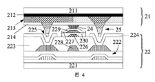
図4は、本発明の他の実施例に係る液晶表示パネルの構造断面図である。本実施例において、同一の構造要素に図2に示す実施例と同一の符号を付する。図4に示すように、図2に示す実施例に比べると、本実施例のアレイ基板22は、タッチ電極229及び誘電体分離層(Interlayer dielectric isolation、ILD。層間誘電体分離とも呼ばれる。)230を更に含む。ここで、パッシベーション層227、タッチ電極229、誘電体分離層230及び共通電極層226は、順にフォトスペーサー24の下方に位置し、フォトスペーサー24は、パッシベーション層227に当接する。
FIG. 4 is a structural sectional view of a liquid crystal display panel according to another embodiment of the present invention. In this embodiment, the same structural elements are designated by the same reference numerals as those in the embodiment shown in FIG. As shown in FIG. 4, as compared with the embodiment shown in FIG. 2, the
本実施例において、タッチ電極229と共通電極層226との間に生じた静電容量の変化を検出すれば、タッチパネル操作を実現することができる。タッチ電極229が液晶表示パネルの内部に設けられるため、本実施例は、in−cell技術を用いた液晶表示パネルと見なすことができる。それに対応して、図2に示す実施例は、非in−cell技術を用いた液晶表示パネルと見なすことができる。
In this embodiment, the touch panel operation can be realized by detecting the change in capacitance generated between the
上述のように、本発明の実施例は、カラーフィルム基板の液晶セルに対向する側に、アレイ基板の片側におけるコンタクトホールに対応して挿入可能な凸柱を設け、凸柱とコンタクトホールとの係合により、カラーフィルム基板とアレイ基板との間の相対的な移動ができるだけ回避され、フォトスペーサーが変位して表示領域に入ることが防止され、フォトスペーサーの安定性が改善され、表示領域に損傷を与えることが回避されることを目的とする。これを基に、本発明の前記実施例を改良することができ、改良される実施例は、全て本発明の保護範囲に属する。 As described above, in the embodiment of the present invention, a convex column that can be inserted corresponding to a contact hole on one side of the array substrate is provided on the side of the color film substrate facing the liquid crystal cell, and the convex column and the contact hole are provided. Engagement avoids relative movement between the color film substrate and the array substrate as much as possible, prevents the photospacer from shifting and entering the display area, improves the stability of the photospacer, and in the display area. The purpose is to avoid damaging it. Based on this, the above-described embodiment of the present invention can be improved, and all the improved examples belong to the protection scope of the present invention.
本発明の実施例は、図5に示す液晶表示装置50を更に提供する。前記液晶表示装置50は、液晶表示パネル51と、液晶表示パネル51に光線を供給する光源モジュール52と、を含む。液晶表示パネル51は、前記図2及び図3に示す実施例に係る液晶表示パネルを含む。前記液晶表示装置50は、前記凸柱及びコンタクトホールの設計を有するため、同じ有益な効果を有する。
Examples of the present invention further provide the liquid
上述した説明は、本発明の実施例に過ぎず、本発明の範囲を限定するものではない。本明細書及び図面の内容に基づいた等価構造又は等価工程の変更、例えば、各実施例間の技術特徴の組み合わせ、又は他の関連技術分野への直接若しくは間接使用は、全て本発明の保護範囲に属する。 The above description is merely an embodiment of the present invention and does not limit the scope of the present invention. Modifications to the equivalent structure or process based on the contents of this specification and drawings, such as the combination of technical features between each embodiment, or direct or indirect use in other related technical fields are all within the scope of the invention. Belongs to.
Claims (12)
互いに対向して離間するように設けられたカラーフィルム基板及びアレイ基板と、
前記カラーフィルム基板と前記アレイ基板との間に設けられたフォトスペーサーと、を含み、
前記アレイ基板の前記カラーフィルム基板に対向する側にコンタクトホールが開設され、前記カラーフィルム基板の前記アレイ基板に対向する側に凸柱が設けられ、前記凸柱の高さは前記フォトスペーサーの高さよりも大きく、前記凸柱の頂部は前記コンタクトホールに挿入され、
前記カラーフィルム基板は、第1の基体と、前記第1の基体の前記アレイ基板に対向する側に形成されるカラーフィルタ層と、前記カラーフィルタ層の前記アレイ基板に対向する側に形成される保護層と、を含み、前記凸柱は、前記カラーフィルタ層及び前記保護層を形成する複数回の露光現像のうちの少なくとも1回で形成され、
前記アレイ基板は、第2の基体と、前記第2の基体に形成された薄膜トランジスタ、平坦化層、画素電極層と、を含み、前記コンタクトホールは、前記平坦化層に開設され、前記画素電極層は、前記コンタクトホールに形成され、前記コンタクトホールを介して前記薄膜トランジスタのドレインに電気的に接続され、
前記アレイ基板は、順に前記フォトスペーサーの下方に位置するパッシベーション層、タッチ電極、誘電体分離層及び共通電極層を更に含み、前記フォトスペーサーは、前記パッシベーション層に当接する、
液晶表示パネル。 It is a liquid crystal display panel
A color film substrate and an array substrate provided so as to face each other and are separated from each other.
Includes a photospacer provided between the color film substrate and the array substrate.
A contact hole is opened on the side of the array substrate facing the color film substrate, a convex pillar is provided on the side of the color film substrate facing the array substrate, and the height of the convex pillar is the height of the photo spacer. Larger than that, the top of the convex column is inserted into the contact hole and
The color film substrate is formed on a first substrate, a color filter layer formed on the side of the first substrate facing the array substrate, and a color filter layer formed on the side of the color filter layer facing the array substrate. The convex column is formed by at least one of a plurality of exposure developments forming the color filter layer and the protective layer, including a protective layer.
The array substrate includes a second substrate, a thin film transistor, a flattening layer, and a pixel electrode layer formed on the second substrate, and the contact hole is formed in the flattening layer to form the pixel electrode. The layer is formed in the contact hole and is electrically connected to the drain of the thin film transistor through the contact hole.
The array substrate further includes a passivation layer, a touch electrode, a dielectric separation layer, and a common electrode layer located below the photo spacer in order, and the photo spacer abuts on the passivation layer.
Liquid crystal display panel.
互いに対向して離間するように設けられたカラーフィルム基板及びアレイ基板と、
前記カラーフィルム基板と前記アレイ基板との間に設けられたフォトスペーサーと、を含み、
前記アレイ基板の前記カラーフィルム基板に対向する側にコンタクトホールが開設され、前記カラーフィルム基板の前記アレイ基板に対向する側に凸柱が設けられ、前記凸柱の高さは前記フォトスペーサーの高さより大きく、前記凸柱の頂部は前記コンタクトホールに挿入され、
前記アレイ基板は、第2の基体と、前記第2の基体に形成された薄膜トランジスタ、平坦化層、画素電極層と、を含み、前記コンタクトホールは、前記平坦化層に開設され、前記画素電極層は、前記コンタクトホールに形成され、前記コンタクトホールを介して前記薄膜トランジスタのドレインに電気的に接続され、
前記アレイ基板は、順に前記フォトスペーサーの下方に位置するパッシベーション層、タッチ電極、誘電体分離層及び共通電極層を更に含み、前記フォトスペーサーは、前記パッシベーション層に当接する、
液晶表示パネル。 It is a liquid crystal display panel
A color film substrate and an array substrate provided so as to face each other and are separated from each other.
Includes a photospacer provided between the color film substrate and the array substrate.
A contact hole is opened on the side of the array substrate facing the color film substrate, a convex pillar is provided on the side of the color film substrate facing the array substrate, and the height of the convex pillar is the height of the photo spacer. Larger, the top of the convex column is inserted into the contact hole
The array substrate includes a second substrate, a thin film transistor, a flattening layer, and a pixel electrode layer formed on the second substrate, and the contact hole is formed in the flattening layer to form the pixel electrode. The layer is formed in the contact hole and is electrically connected to the drain of the thin film transistor through the contact hole.
The array substrate further includes a passivation layer, a touch electrode, a dielectric separation layer, and a common electrode layer located below the photo spacer in order, and the photo spacer abuts on the passivation layer.
Liquid crystal display panel.
請求項2に記載の液晶表示パネル。 The color film substrate includes a first substrate and a color filter layer formed on the side of the first substrate facing the array substrate, and the convex pillars form a plurality of the color filter layer. Formed at least once of exposure and development,
The liquid crystal display panel according to claim 2.
請求項2に記載の液晶表示パネル。 The color film substrate is formed on a first substrate, a color filter layer formed on the side of the first substrate facing the array substrate, and a color filter layer formed on the side of the color filter layer facing the array substrate. The convex column is formed by at least one of a plurality of exposure developments forming the color filter layer and the protective layer, including a protective layer.
The liquid crystal display panel according to claim 2.
請求項4に記載の液晶表示パネル。 The color film substrate further includes a black matrix layer formed between the first substrate and the color filter layer.
The liquid crystal display panel according to claim 4.
請求項4に記載の液晶表示パネル。 The color filter layer includes a red filter, a green filter, a blue filter and a white filter.
The liquid crystal display panel according to claim 4.
前記液晶表示パネルは、
互いに対向して離間するように設けられたカラーフィルム基板及びアレイ基板と、
前記カラーフィルム基板と前記アレイ基板との間に設けられたフォトスペーサーと、を含み、
前記アレイ基板の前記カラーフィルム基板に対向する側にコンタクトホールが開設され、前記カラーフィルム基板の前記アレイ基板に対向する側に凸柱が設けられ、前記凸柱の高さは、前記フォトスペーサーの高さよりも大きく、前記凸柱の頂部は、前記コンタクトホールに挿入され、
前記アレイ基板は、第2の基体と、前記第2の基体に形成された薄膜トランジスタ、平坦化層、画素電極層と、を含み、前記コンタクトホールは、前記平坦化層に開設され、前記画素電極層は、前記コンタクトホールに形成され、前記コンタクトホールを介して前記薄膜トランジスタのドレインに電気的に接続され、
前記アレイ基板は、順に前記フォトスペーサーの下方に位置するパッシベーション層、タッチ電極、誘電体分離層及び共通電極層を更に含み、前記フォトスペーサーは、前記パッシベーション層に当接する、
液晶表示装置。 A liquid crystal display device including a liquid crystal display panel and a light source module that supplies light rays to the liquid crystal display panel.
The liquid crystal display panel
A color film substrate and an array substrate provided so as to face each other and are separated from each other.
Includes a photospacer provided between the color film substrate and the array substrate.
A contact hole is opened on the side of the array substrate facing the color film substrate, a convex pillar is provided on the side of the color film substrate facing the array substrate, and the height of the convex pillar is the height of the photo spacer. Larger than the height, the top of the convex column is inserted into the contact hole and
The array substrate includes a second substrate, a thin film transistor, a flattening layer, and a pixel electrode layer formed on the second substrate, and the contact hole is formed in the flattening layer to form the pixel electrode. The layer is formed in the contact hole and is electrically connected to the drain of the thin film transistor through the contact hole.
The array substrate further includes a passivation layer, a touch electrode, a dielectric separation layer, and a common electrode layer located below the photo spacer in order, and the photo spacer abuts on the passivation layer.
Liquid crystal display device.
請求項8に記載の液晶表示装置。 The color film substrate includes a first substrate and a color filter layer formed on the side of the first substrate facing the array substrate, and the convex pillars form a plurality of the color filter layer. Formed at least once of exposure and development,
The liquid crystal display device according to claim 8.
請求項8に記載の液晶表示装置。 The color film substrate is formed on a first substrate, a color filter layer formed on the side of the first substrate facing the array substrate, and a color filter layer formed on the side of the color filter layer facing the array substrate. The convex column is formed by at least one of a plurality of exposure developments forming the color filter layer and the protective layer, including a protective layer.
The liquid crystal display device according to claim 8.
請求項10に記載の液晶表示装置。 The color film substrate further includes a black matrix layer formed between the first substrate and the color filter layer.
The liquid crystal display device according to claim 10.
請求項9に記載の液晶表示装置。 The color filter layer includes a red filter, a green filter and a blue filter, or the color filter layer includes a red filter, a green filter, a blue filter and a white filter.
The liquid crystal display device according to claim 9.
Applications Claiming Priority (3)
| Application Number | Priority Date | Filing Date | Title |
|---|---|---|---|
| CN201610695291.XA CN106125390A (en) | 2016-08-19 | 2016-08-19 | Display panels and liquid crystal indicator |
| CN201610695291.X | 2016-08-19 | ||
| PCT/CN2016/098172 WO2018032551A1 (en) | 2016-08-19 | 2016-09-06 | Liquid crystal display panel and liquid crystal display device |
Publications (2)
| Publication Number | Publication Date |
|---|---|
| JP2019525256A JP2019525256A (en) | 2019-09-05 |
| JP6854882B2 true JP6854882B2 (en) | 2021-04-07 |
Family
ID=57279083
Family Applications (1)
| Application Number | Title | Priority Date | Filing Date |
|---|---|---|---|
| JP2019509477A Active JP6854882B2 (en) | 2016-08-19 | 2016-09-06 | Liquid crystal display panel and liquid crystal display device |
Country Status (6)
| Country | Link |
|---|---|
| US (1) | US10180601B2 (en) |
| EP (1) | EP3502774B1 (en) |
| JP (1) | JP6854882B2 (en) |
| KR (1) | KR20190032492A (en) |
| CN (1) | CN106125390A (en) |
| WO (1) | WO2018032551A1 (en) |
Families Citing this family (11)
| Publication number | Priority date | Publication date | Assignee | Title |
|---|---|---|---|---|
| CN106371236A (en) * | 2016-10-24 | 2017-02-01 | 厦门天马微电子有限公司 | Display panel and display device |
| CN106950736A (en) * | 2017-04-05 | 2017-07-14 | 惠科股份有限公司 | Contact surface plate and its manufacture method |
| CN107490904A (en) * | 2017-08-25 | 2017-12-19 | 惠科股份有限公司 | Liquid crystal display panel and liquid crystal display device |
| CN107706212B (en) * | 2017-09-06 | 2019-08-30 | 武汉华星光电半导体显示技术有限公司 | A kind of preparation method and display panel of display panel |
| CN107797332A (en) * | 2017-11-22 | 2018-03-13 | 深圳市华星光电技术有限公司 | A kind of liquid crystal display panel and liquid crystal display device |
| KR102543486B1 (en) * | 2018-02-20 | 2023-06-14 | 삼성디스플레이 주식회사 | Display device |
| CN207992626U (en) * | 2018-02-23 | 2018-10-19 | 京东方科技集团股份有限公司 | A kind of substrate, mask plate, display panel and display device |
| CN108508658B (en) * | 2018-03-30 | 2020-12-25 | 京东方科技集团股份有限公司 | Color film substrate, manufacturing method of color film substrate and display panel |
| KR102573550B1 (en) * | 2018-08-31 | 2023-08-31 | 엘지디스플레이 주식회사 | Light Emitting Display Device and Manufacturing Method thereof |
| CN109164677B (en) * | 2018-09-05 | 2021-12-07 | 京东方科技集团股份有限公司 | Photoetching method, preparation method of flexible substrate and photoresist drying device |
| CN113359357B (en) * | 2021-06-17 | 2022-08-05 | 武汉华星光电技术有限公司 | Liquid crystal display panel and liquid crystal display device |
Family Cites Families (27)
| Publication number | Priority date | Publication date | Assignee | Title |
|---|---|---|---|---|
| JP3999824B2 (en) * | 1995-08-21 | 2007-10-31 | 東芝電子エンジニアリング株式会社 | Liquid crystal display element |
| JP3757079B2 (en) * | 1999-05-26 | 2006-03-22 | Nec液晶テクノロジー株式会社 | Color liquid crystal display device |
| TW554221B (en) * | 2001-01-09 | 2003-09-21 | Matsushita Electric Ind Co Ltd | Liquid crystal display device and manufacturing method thereof |
| US7583279B2 (en) * | 2004-04-09 | 2009-09-01 | Samsung Electronics Co., Ltd. | Subpixel layouts and arrangements for high brightness displays |
| KR20050043220A (en) * | 2003-11-05 | 2005-05-11 | 엘지.필립스 엘시디 주식회사 | Fabrication method of liquid crystal display device using color filter substrate formed by back exposure and structure of the same |
| KR100740041B1 (en) * | 2005-06-30 | 2007-07-16 | 엘지.필립스 엘시디 주식회사 | Liquid crystal panel having dual column spacer, and method for manufacturing the same |
| KR101192761B1 (en) * | 2005-11-29 | 2012-10-18 | 엘지디스플레이 주식회사 | Liquid Crystal Display Device and method of manufacturing the same |
| US7626675B2 (en) | 2006-04-20 | 2009-12-01 | Chungwa Picture Tubes, Ltd. | Color filter substrate and liquid crystal display panel with spacer having a recess or clipping opening in which an active device is wedged therein |
| CN101071210A (en) * | 2006-05-08 | 2007-11-14 | 中华映管股份有限公司 | Colour filter substrate and its liquid crystal display panel |
| JP2009069391A (en) * | 2007-09-12 | 2009-04-02 | Hitachi Displays Ltd | Liquid crystal display device |
| KR20090097565A (en) * | 2008-03-12 | 2009-09-16 | 삼성전자주식회사 | Liquid crystal display panel and method for manufacturing the liquid crystal display panel |
| JP5191453B2 (en) * | 2009-06-29 | 2013-05-08 | 株式会社ジャパンディスプレイウェスト | Touch sensor, display device, and electronic device |
| JP5077367B2 (en) * | 2010-01-28 | 2012-11-21 | 凸版印刷株式会社 | Color filter substrate for transflective liquid crystal display device, manufacturing method thereof, and transflective liquid crystal display device |
| KR20120033688A (en) | 2010-09-30 | 2012-04-09 | 엘지디스플레이 주식회사 | Liquid crystal display device |
| CN102109628A (en) * | 2011-01-28 | 2011-06-29 | 深圳市华星光电技术有限公司 | Structure of CF (color filter) and manufacture method thereof |
| JP5450516B2 (en) * | 2011-06-20 | 2014-03-26 | 株式会社ジャパンディスプレイ | Liquid crystal display |
| JP5837350B2 (en) * | 2011-07-21 | 2015-12-24 | 株式会社ジャパンディスプレイ | Liquid crystal display |
| KR101524449B1 (en) * | 2011-12-22 | 2015-06-02 | 엘지디스플레이 주식회사 | Liquid crystal display device and Method for manufacturing the same |
| KR101466556B1 (en) * | 2012-03-29 | 2014-11-28 | 엘지디스플레이 주식회사 | Liquid crystal display device and Method for manufacturing the same |
| CN102955297B (en) * | 2012-10-22 | 2015-09-09 | 京东方科技集团股份有限公司 | A kind of display panels and preparation method thereof |
| CN103033981B (en) * | 2013-01-09 | 2016-05-11 | 深圳市华星光电技术有限公司 | Colored filter substrate and manufacture method thereof and liquid crystal panel |
| JP2016031513A (en) * | 2014-07-30 | 2016-03-07 | 大日本印刷株式会社 | High-definition color filter |
| CN104597656B (en) * | 2015-02-13 | 2018-04-06 | 深圳市华星光电技术有限公司 | Color membrane substrates, manufacture method and liquid crystal panel |
| US9910530B2 (en) * | 2015-02-27 | 2018-03-06 | Panasonic Liquid Crystal Display Co., Ltd. | Display panel with touch detection function |
| CN104880865B (en) * | 2015-06-19 | 2019-03-19 | 武汉华星光电技术有限公司 | Array substrate and preparation method thereof, liquid crystal display panel |
| US20170017338A1 (en) * | 2015-07-17 | 2017-01-19 | Innolux Corporation | Touch display device |
| CN105093742B (en) * | 2015-08-06 | 2019-01-22 | 武汉华星光电技术有限公司 | array substrate, liquid crystal display panel and liquid crystal display |
-
2016
- 2016-08-19 CN CN201610695291.XA patent/CN106125390A/en active Pending
- 2016-09-06 JP JP2019509477A patent/JP6854882B2/en active Active
- 2016-09-06 WO PCT/CN2016/098172 patent/WO2018032551A1/en active Application Filing
- 2016-09-06 KR KR1020197005171A patent/KR20190032492A/en not_active Application Discontinuation
- 2016-09-06 EP EP16913307.1A patent/EP3502774B1/en active Active
- 2016-09-06 US US15/128,398 patent/US10180601B2/en active Active
Also Published As
| Publication number | Publication date |
|---|---|
| US20180180920A1 (en) | 2018-06-28 |
| US10180601B2 (en) | 2019-01-15 |
| EP3502774B1 (en) | 2023-01-04 |
| EP3502774A4 (en) | 2020-01-22 |
| CN106125390A (en) | 2016-11-16 |
| WO2018032551A1 (en) | 2018-02-22 |
| JP2019525256A (en) | 2019-09-05 |
| KR20190032492A (en) | 2019-03-27 |
| EP3502774A1 (en) | 2019-06-26 |
Similar Documents
| Publication | Publication Date | Title |
|---|---|---|
| JP6854882B2 (en) | Liquid crystal display panel and liquid crystal display device | |
| US9851600B2 (en) | Liquid crystal display panel and manufacturing method thereof | |
| KR101954979B1 (en) | Color filter substrate, Liquid crystal display apparatus and method for fabricating color filter | |
| US9606392B2 (en) | Display panel and liquid crystal display including the same | |
| EP3312668B1 (en) | Array substrate and method for manufacturing same, and display device | |
| KR101835545B1 (en) | Liquid crystal display device and Method for manufacturing the same | |
| US9595549B2 (en) | Display device comprising a plurality of microcavities and an encapsulation layer that seals the plurality of microcavities and method of manufacturing the same | |
| US20210041730A1 (en) | Display panel, manufacturing method thereof and display device | |
| JP5503300B2 (en) | Method for manufacturing liquid crystal display device, liquid crystal display device and electronic apparatus | |
| KR20140095120A (en) | Display device and manufacturing method thereof | |
| KR20140082049A (en) | Display device and manufacturing method thereof | |
| WO2017193633A1 (en) | Display substrate and preparation method therefor, and display device | |
| US9116297B2 (en) | Color filter substrate, manufacturing method thereof and liquid crystal panel | |
| EP2808729A1 (en) | Display device and manufacturing method thereof | |
| KR20150097889A (en) | Liquid crystal display | |
| JP2007316329A (en) | Liquid crystal display device and manufacturing method thereof | |
| WO2019075887A1 (en) | Array substrate and display panel | |
| KR20140097782A (en) | Liquid Crystal Display Device and Method of manufacturing the sames | |
| US20160202520A1 (en) | Display device and related manufacturing method | |
| US20160154286A1 (en) | Liquid crystal display device and method of manufacturing the same | |
| US9477110B2 (en) | Display device and manufacturing method thereof | |
| US20160291394A1 (en) | Liquid crystal display device and method of manufacturing the same | |
| JP2011180549A (en) | Liquid crystal display device, method of manufacturing the same, and electronic apparatus | |
| JP2012078479A (en) | Liquid crystal display device | |
| KR20050090643A (en) | Liquid crystal display device and method for fabricating the same |
Legal Events
| Date | Code | Title | Description |
|---|---|---|---|
| A621 | Written request for application examination |
Free format text: JAPANESE INTERMEDIATE CODE: A621 Effective date: 20190218 |
|
| A131 | Notification of reasons for refusal |
Free format text: JAPANESE INTERMEDIATE CODE: A131 Effective date: 20191217 |
|
| A977 | Report on retrieval |
Free format text: JAPANESE INTERMEDIATE CODE: A971007 Effective date: 20191218 |
|
| A521 | Request for written amendment filed |
Free format text: JAPANESE INTERMEDIATE CODE: A523 Effective date: 20200317 |
|
| A131 | Notification of reasons for refusal |
Free format text: JAPANESE INTERMEDIATE CODE: A131 Effective date: 20200902 |
|
| A521 | Request for written amendment filed |
Free format text: JAPANESE INTERMEDIATE CODE: A523 Effective date: 20201014 |
|
| TRDD | Decision of grant or rejection written | ||
| A01 | Written decision to grant a patent or to grant a registration (utility model) |
Free format text: JAPANESE INTERMEDIATE CODE: A01 Effective date: 20210312 |
|
| A61 | First payment of annual fees (during grant procedure) |
Free format text: JAPANESE INTERMEDIATE CODE: A61 Effective date: 20210316 |
|
| R150 | Certificate of patent or registration of utility model |
Ref document number: 6854882 Country of ref document: JP Free format text: JAPANESE INTERMEDIATE CODE: R150 |
|
| R250 | Receipt of annual fees |
Free format text: JAPANESE INTERMEDIATE CODE: R250 |