JP6851838B2 - Laminated lens structure, camera module, and electronics - Google Patents

Laminated lens structure, camera module, and electronics Download PDF

Info

Publication number
JP6851838B2
JP6851838B2 JP2017011989A JP2017011989A JP6851838B2 JP 6851838 B2 JP6851838 B2 JP 6851838B2 JP 2017011989 A JP2017011989 A JP 2017011989A JP 2017011989 A JP2017011989 A JP 2017011989A JP 6851838 B2 JP6851838 B2 JP 6851838B2
Authority
JP
Japan
Prior art keywords
lens
substrate
resin
laminated
camera module
Prior art date
Legal status (The legal status is an assumption and is not a legal conclusion. Google has not performed a legal analysis and makes no representation as to the accuracy of the status listed.)
Active
Application number
JP2017011989A
Other languages
Japanese (ja)
Other versions
JP2018120112A (en
JP2018120112A5 (en
Inventor
光成 星
光成 星
根来 陽一
陽一 根来
Current Assignee (The listed assignees may be inaccurate. Google has not performed a legal analysis and makes no representation or warranty as to the accuracy of the list.)
Sony Semiconductor Solutions Corp
Original Assignee
Sony Semiconductor Solutions Corp
Priority date (The priority date is an assumption and is not a legal conclusion. Google has not performed a legal analysis and makes no representation as to the accuracy of the date listed.)
Filing date
Publication date
Application filed by Sony Semiconductor Solutions Corp filed Critical Sony Semiconductor Solutions Corp
Priority to JP2017011989A priority Critical patent/JP6851838B2/en
Priority to KR1020197015135A priority patent/KR102508561B1/en
Priority to US16/477,975 priority patent/US11493671B2/en
Priority to PCT/JP2018/000954 priority patent/WO2018139259A1/en
Priority to CN201880007604.5A priority patent/CN110199215B/en
Publication of JP2018120112A publication Critical patent/JP2018120112A/en
Publication of JP2018120112A5 publication Critical patent/JP2018120112A5/ja
Application granted granted Critical
Publication of JP6851838B2 publication Critical patent/JP6851838B2/en
Active legal-status Critical Current
Anticipated expiration legal-status Critical

Links

Images

Classifications

    • GPHYSICS
    • G02OPTICS
    • G02BOPTICAL ELEMENTS, SYSTEMS OR APPARATUS
    • G02B3/00Simple or compound lenses
    • G02B3/0006Arrays
    • G02B3/0037Arrays characterized by the distribution or form of lenses
    • G02B3/0062Stacked lens arrays, i.e. refractive surfaces arranged in at least two planes, without structurally separate optical elements in-between
    • G02B3/0068Stacked lens arrays, i.e. refractive surfaces arranged in at least two planes, without structurally separate optical elements in-between arranged in a single integral body or plate, e.g. laminates or hybrid structures with other optical elements
    • BPERFORMING OPERATIONS; TRANSPORTING
    • B29WORKING OF PLASTICS; WORKING OF SUBSTANCES IN A PLASTIC STATE IN GENERAL
    • B29DPRODUCING PARTICULAR ARTICLES FROM PLASTICS OR FROM SUBSTANCES IN A PLASTIC STATE
    • B29D11/00Producing optical elements, e.g. lenses or prisms
    • B29D11/00009Production of simple or compound lenses
    • B29D11/00365Production of microlenses
    • B29D11/00375Production of microlenses by moulding lenses in holes through a substrate
    • BPERFORMING OPERATIONS; TRANSPORTING
    • B29WORKING OF PLASTICS; WORKING OF SUBSTANCES IN A PLASTIC STATE IN GENERAL
    • B29DPRODUCING PARTICULAR ARTICLES FROM PLASTICS OR FROM SUBSTANCES IN A PLASTIC STATE
    • B29D11/00Producing optical elements, e.g. lenses or prisms
    • B29D11/00009Production of simple or compound lenses
    • B29D11/00403Producing compound lenses
    • GPHYSICS
    • G02OPTICS
    • G02BOPTICAL ELEMENTS, SYSTEMS OR APPARATUS
    • G02B7/00Mountings, adjusting means, or light-tight connections, for optical elements
    • G02B7/02Mountings, adjusting means, or light-tight connections, for optical elements for lenses
    • G02B7/021Mountings, adjusting means, or light-tight connections, for optical elements for lenses for more than one lens
    • GPHYSICS
    • G03PHOTOGRAPHY; CINEMATOGRAPHY; ANALOGOUS TECHNIQUES USING WAVES OTHER THAN OPTICAL WAVES; ELECTROGRAPHY; HOLOGRAPHY
    • G03BAPPARATUS OR ARRANGEMENTS FOR TAKING PHOTOGRAPHS OR FOR PROJECTING OR VIEWING THEM; APPARATUS OR ARRANGEMENTS EMPLOYING ANALOGOUS TECHNIQUES USING WAVES OTHER THAN OPTICAL WAVES; ACCESSORIES THEREFOR
    • G03B30/00Camera modules comprising integrated lens units and imaging units, specially adapted for being embedded in other devices, e.g. mobile phones or vehicles
    • HELECTRICITY
    • H04ELECTRIC COMMUNICATION TECHNIQUE
    • H04NPICTORIAL COMMUNICATION, e.g. TELEVISION
    • H04N23/00Cameras or camera modules comprising electronic image sensors; Control thereof
    • H04N23/50Constructional details
    • H04N23/55Optical parts specially adapted for electronic image sensors; Mounting thereof

Description

本技術は、積層レンズ構造体、カメラモジュール、および、電子機器に関し、特に、レンズ樹脂の硬化収縮による変形を低減することができるようにした積層レンズ構造体、カメラモジュール、および、電子機器に関する。 The present technology relates to a laminated lens structure, a camera module, and an electronic device, and more particularly to a laminated lens structure, a camera module, and an electronic device capable of reducing deformation due to curing shrinkage of the lens resin.

ウエハ基板の平面方向にレンズを複数配列させるウエハレベルレンズプロセスは、レンズを形成する際の形状精度や位置精度の要求が厳しい。 In the wafer level lens process in which a plurality of lenses are arranged in the plane direction of the wafer substrate, there are strict requirements for shape accuracy and position accuracy when forming the lens.

ウエハレベルレンズプロセスについては、これまでも様々な技術が考案され、提案されている。ウエハレベルレンズプロセスでは、基板に形成した貫通孔内にレンズ材料である熱可塑性樹脂や熱硬化性樹脂などが充填された後、金型で成形してレンズ部が形成される(例えば、特許文献1参照)。 Various techniques have been devised and proposed for the wafer level lens process. In the wafer level lens process, a lens material such as a thermoplastic resin or a thermosetting resin is filled in a through hole formed in a substrate, and then molded with a mold to form a lens portion (for example, Patent Document). 1).

特開2009−300596号公報JP-A-2009-300596

ウエハレベルレンズプロセスでは、製造時のレンズ樹脂の硬化収縮により、例えば、レンズ形状が型と異なってしまったり、基板が反ってしまうことがある。 In the wafer level lens process, for example, the lens shape may be different from the mold or the substrate may be warped due to the curing shrinkage of the lens resin during manufacturing.

本技術は、このような状況に鑑みてなされたものであり、レンズ樹脂の硬化収縮による変形を低減することができるようにするものである。 This technique has been made in view of such a situation, and makes it possible to reduce the deformation of the lens resin due to curing shrinkage.

本技術の第1の側面の積層レンズ構造体は、基板に形成された貫通孔の内側にレンズ樹脂部が配置されたレンズ付き基板どうしが直接接合により接合されて積層されており、前記レンズ樹脂部は、光を屈折させるレンズとしての性能を有するレンズ部と、前記レンズ部を前記基板に担持する担持部とを有し、前記担持部の厚みの最も薄い部分である最薄部の厚み方向の中心位置が、前記レンズ部の中央部の厚み方向の中心位置と、前記レンズ部の外周部の厚み方向の中心位置との間に位置する。 In the laminated lens structure on the first side surface of the present technology, substrates with lenses in which a lens resin portion is arranged inside a through hole formed in the substrate are directly bonded and laminated, and the lens resin is said to be laminated. The portion has a lens portion having a performance as a lens that refracts light and a supporting portion that supports the lens portion on the substrate, and the thickness direction of the thinnest portion that is the thinnest portion of the supporting portion. Is located between the center position of the central portion of the lens portion in the thickness direction and the center position of the outer peripheral portion of the lens portion in the thickness direction.

本技術の第1の側面においては、基板に形成された貫通孔の内側にレンズ樹脂部が配置されたレンズ付き基板どうしが直接接合により接合されて積層されており、前記レンズ樹脂部には、光を屈折させるレンズとしての性能を有するレンズ部と、前記レンズ部を前記基板に担持する担持部とが設けられ、前記担持部の厚みの最も薄い部分である最薄部の厚み方向の中心位置が、前記レンズ部の中央部の厚み方向の中心位置と、前記レンズ部の外周部の厚み方向の中心位置との間に位置するように構成される。 In the first aspect of the present technology, the lenses-equipped substrates in which the lens resin portion is arranged inside the through hole formed in the substrate are joined and laminated by direct bonding, and the lens resin portion is formed with the lens resin portion. A lens portion having a performance as a lens that refracts light and a supporting portion that supports the lens portion on the substrate are provided, and a central position in the thickness direction of the thinnest portion, which is the thinnest portion of the supporting portion. Is configured to be located between the center position of the central portion of the lens portion in the thickness direction and the center position of the outer peripheral portion of the lens portion in the thickness direction.

本技術の第の側面のカメラモジュールは、基板に形成された貫通孔の内側にレンズ樹脂部が配置されたレンズ付き基板どうしが直接接合により接合されて積層されており、前記レンズ樹脂部は、光を屈折させるレンズとしての性能を有するレンズ部と、前記レンズ部を前記基板に接合する担持部とを有し、前記担持部の厚みの最も薄い最薄部の厚み方向の中心位置が、前記レンズ部の中央部の厚み方向の中心位置と、前記レンズ部の外周部の厚み方向の中心位置との間に位置する積層レンズ構造体を備える。 In the camera module on the second side surface of the present technology, substrates with lenses in which a lens resin portion is arranged inside a through hole formed in the substrate are directly bonded and laminated, and the lens resin portion is laminated. The center position in the thickness direction of the thinnest portion, which has a lens portion having a performance as a lens for refracting light and a supporting portion for joining the lens portion to the substrate, is the thinnest of the supporting portions. A laminated lens structure located between the center position of the central portion of the lens portion in the thickness direction and the center position of the outer peripheral portion of the lens portion in the thickness direction is provided.

本技術の第の側面においては、基板に形成された貫通孔の内側にレンズ樹脂部が配置されたレンズ付き基板どうしが直接接合により接合されて積層されており、前記レンズ樹脂部は、光を屈折させるレンズとしての性能を有するレンズ部と、前記レンズ部を前記基板に接合する担持部とを有し、前記担持部の厚みの最も薄い最薄部の厚み方向の中心位置が、前記レンズ部の中央部の厚み方向の中心位置と、前記レンズ部の外周部の厚み方向の中心位置との間に位置する積層レンズ構造体が設けられる。 In the second aspect of the present technology, the lenses-equipped substrates in which the lens resin portion is arranged inside the through hole formed in the substrate are joined and laminated by direct bonding, and the lens resin portion is formed by light. The lens has a lens portion having a performance as a lens that refracts the lens and a supporting portion that joins the lens portion to the substrate, and the center position in the thickness direction of the thinnest portion having the thinnest thickness of the supporting portion is the lens. A laminated lens structure located between the center position in the thickness direction of the central portion of the portion and the center position in the thickness direction of the outer peripheral portion of the lens portion is provided.

本技術の第の側面の電子機器は、基板に形成された貫通孔の内側にレンズ樹脂部が配置されたレンズ付き基板どうしが直接接合により接合されて積層されており、前記レンズ樹脂部は、光を屈折させるレンズとしての性能を有するレンズ部と、前記レンズ部を前記基板に接合する担持部とを有し、前記担持部の厚みの最も薄い最薄部の厚み方向の中心位置が、前記レンズ部の中央部の厚み方向の中心位置と、前記レンズ部の外周部の厚み方向の中心位置との間に位置する積層レンズ構造体を備えるカメラモジュールを備える。 In the electronic device on the third side surface of the present technology, the lenses-equipped substrates in which the lens resin portion is arranged inside the through hole formed in the substrate are joined and laminated by direct bonding, and the lens resin portion is laminated. The center position in the thickness direction of the thinnest portion, which has a lens portion having a performance as a lens for refracting light and a supporting portion for joining the lens portion to the substrate, is the thinnest of the supporting portions. The camera module includes a laminated lens structure located between the center position of the central portion of the lens portion in the thickness direction and the center position of the outer peripheral portion of the lens portion in the thickness direction.

本技術の第の側面においては、基板に形成された貫通孔の内側にレンズ樹脂部が配置されたレンズ付き基板どうしが直接接合により接合されて積層されており、前記レンズ樹脂部は、光を屈折させるレンズとしての性能を有するレンズ部と、前記レンズ部を前記基板に接合する担持部とを有し、前記担持部の厚みの最も薄い最薄部の厚み方向の中心位置が、前記レンズ部の中央部の厚み方向の中心位置と、前記レンズ部の外周部の厚み方向の中心位置との間に位置する積層レンズ構造体を備えるカメラモジュールが設けられる。 In the third aspect of the present technology, the lenses-equipped substrates in which the lens resin portion is arranged inside the through hole formed in the substrate are joined and laminated by direct bonding, and the lens resin portion is formed by light. The lens has a lens portion having a performance as a lens for refracting the lens and a supporting portion for joining the lens portion to the substrate, and the center position in the thickness direction of the thinnest portion having the thinnest thickness of the supporting portion is the lens. A camera module including a laminated lens structure located between the center position in the thickness direction of the central portion of the portion and the center position in the thickness direction of the outer peripheral portion of the lens portion is provided.

積層レンズ構造体、カメラモジュール、及び、電子機器は、独立した装置であっても良いし、他の装置に組み込まれるモジュールであっても良い。 The laminated lens structure, the camera module, and the electronic device may be an independent device or a module incorporated in another device.

本技術の第1乃至第の側面によれば、レンズ樹脂の硬化収縮による変形を低減することができる。 According to the first to third aspects of the present technology, it is possible to reduce the deformation of the lens resin due to curing shrinkage.

なお、ここに記載された効果は必ずしも限定されるものではなく、本開示中に記載されたいずれかの効果であってもよい。 The effects described here are not necessarily limited, and may be any of the effects described in the present disclosure.

本技術を適用した積層レンズ構造体を用いたカメラモジュールの第1の実施の形態を示す図である。It is a figure which shows the 1st Embodiment of the camera module using the laminated lens structure to which this technique is applied. 特許文献1に開示された積層レンズ構造体の断面構造図である。It is sectional drawing of the laminated lens structure disclosed in Patent Document 1. 図1のカメラモジュールの積層レンズ構造体の断面構造図である。It is sectional drawing of the laminated lens structure of the camera module of FIG. レンズ付き基板の直接接合を説明する図である。It is a figure explaining the direct bonding of the substrate with a lens. 図1のカメラモジュールを形成する工程を示す図である。It is a figure which shows the process of forming the camera module of FIG. 図1のカメラモジュールを形成する工程を示す図である。It is a figure which shows the process of forming the camera module of FIG. 図1のカメラモジュールを形成する別の工程を示す図である。It is a figure which shows another process which forms the camera module of FIG. レンズ付き基板の構成を説明する図である。It is a figure explaining the structure of the substrate with a lens. 本技術を適用した積層レンズ構造体を用いたカメラモジュールの第2の実施の形態を示す図である。It is a figure which shows the 2nd Embodiment of the camera module using the laminated lens structure to which this technique is applied. 本技術を適用した積層レンズ構造体を用いたカメラモジュールの第3の実施の形態を示す図である。It is a figure which shows the 3rd Embodiment of the camera module using the laminated lens structure to which this technique is applied. 本技術を適用した積層レンズ構造体を用いたカメラモジュールの第4の実施の形態を示す図である。It is a figure which shows the 4th Embodiment of the camera module using the laminated lens structure to which this technique is applied. 本技術を適用した積層レンズ構造体を用いたカメラモジュールの第5の実施の形態を示す図である。It is a figure which shows the 5th Embodiment of the camera module using the laminated lens structure to which this technique is applied. 第4の実施の形態に係るカメラモジュールの詳細構成を説明する図である。It is a figure explaining the detailed structure of the camera module which concerns on 4th Embodiment. 担体基板とレンズ樹脂部の平面図と断面図である。It is a top view and a cross-sectional view of a carrier substrate and a lens resin part. 積層レンズ構造体と絞り板を示す断面図である。It is sectional drawing which shows the laminated lens structure and the diaphragm plate. 本技術を適用した積層レンズ構造体を用いたカメラモジュールの第6の実施の形態を示す図である。It is a figure which shows the 6th Embodiment of the camera module using the laminated lens structure to which this technique is applied. 本技術を適用した積層レンズ構造体を用いたカメラモジュールの第7の実施の形態を示す図である。It is a figure which shows the 7th Embodiment of the camera module using the laminated lens structure to which this technique is applied. レンズ付き基板の詳細構成を示す断面図である。It is sectional drawing which shows the detailed structure of the substrate with a lens. レンズ付き基板の製造方法を説明する図である。It is a figure explaining the manufacturing method of the substrate with a lens. レンズ付き基板の製造方法を説明する図である。It is a figure explaining the manufacturing method of the substrate with a lens. レンズ付き基板の製造方法を説明する図である。It is a figure explaining the manufacturing method of the substrate with a lens. レンズ付き基板の製造方法を説明する図である。It is a figure explaining the manufacturing method of the substrate with a lens. レンズ付き基板の製造方法を説明する図である。It is a figure explaining the manufacturing method of the substrate with a lens. レンズ付き基板の製造方法を説明する図である。It is a figure explaining the manufacturing method of the substrate with a lens. レンズ付き基板の製造方法を説明する図である。It is a figure explaining the manufacturing method of the substrate with a lens. レンズ付き基板の製造方法を説明する図である。It is a figure explaining the manufacturing method of the substrate with a lens. レンズ付き基板の製造方法を説明する図である。It is a figure explaining the manufacturing method of the substrate with a lens. レンズ付き基板の製造方法を説明する図である。It is a figure explaining the manufacturing method of the substrate with a lens. レンズ付き基板の製造方法を説明する図である。It is a figure explaining the manufacturing method of the substrate with a lens. 基板状態のレンズ付き基板どうしの接合を説明する図である。It is a figure explaining the joining of the substrate with a lens in the substrate state. 基板状態のレンズ付き基板どうしの接合を説明する図である。It is a figure explaining the joining of the substrate with a lens in the substrate state. 5枚のレンズ付き基板を基板状態で積層する第1の積層方法を説明する図である。It is a figure explaining the 1st laminating method of laminating 5 substrates with a lens in a substrate state. 5枚のレンズ付き基板を基板状態で積層する第2の積層方法を説明する図である。It is a figure explaining the 2nd laminating method of laminating 5 substrates with a lens in a substrate state. 本技術を適用した積層レンズ構造体を用いたカメラモジュールの第8の実施の形態を示す図である。It is a figure which shows the 8th Embodiment of the camera module using the laminated lens structure to which this technique is applied. 本技術を適用した積層レンズ構造体を用いたカメラモジュールの第9の実施の形態を示す図である。It is a figure which shows the 9th Embodiment of the camera module using the laminated lens structure to which this technique is applied. 本技術を適用した積層レンズ構造体を用いたカメラモジュールの第10の実施の形態を示す図である。It is a figure which shows the tenth embodiment of the camera module using the laminated lens structure to which this technique is applied. 本技術を適用した積層レンズ構造体を用いたカメラモジュールの第11の実施の形態を示す図である。It is a figure which shows the eleventh embodiment of the camera module using the laminated lens structure to which this technique is applied. 比較構造例1としてのウエハレベル積層構造の断面図である。It is sectional drawing of the wafer level laminated structure as a comparative structure example 1. FIG. 比較構造例2としてのレンズアレイ基板の断面図である。It is sectional drawing of the lens array substrate as a comparative structure example 2. FIG. 図39のレンズアレイ基板の製造方法を説明する図である。It is a figure explaining the manufacturing method of the lens array substrate of FIG. 比較構造例3としてのレンズアレイ基板の断面図である。It is sectional drawing of the lens array substrate as a comparative structure example 3. FIG. 図41のレンズアレイ基板の製造方法を説明する図である。It is a figure explaining the manufacturing method of the lens array substrate of FIG. 41. 比較構造例4としてのレンズアレイ基板の断面図である。It is sectional drawing of the lens array substrate as a comparative structure example 4. FIG. 図43のレンズアレイ基板の製造方法を説明する図である。It is a figure explaining the manufacturing method of the lens array substrate of FIG. 43. 比較構造例5としてのレンズアレイ基板の断面図である。It is sectional drawing of the lens array substrate as a comparative structure example 5. レンズとなる樹脂がもたらす作用を説明する図である。It is a figure explaining the action which the resin which becomes a lens brings. レンズとなる樹脂がもたらす作用を説明する図である。It is a figure explaining the action which the resin which becomes a lens brings. 比較構造例6としてのレンズアレイ基板を模式的に表した図である。It is a figure which represented typically the lens array substrate as a comparative structure example 6. 比較構造例7としての積層レンズ構造体の断面図である。It is sectional drawing of the laminated lens structure as a comparative structure example 7. 図49の積層レンズ構造体がもたらす作用を説明する図である。It is a figure explaining the action which the laminated lens structure of FIG. 49 brings. 比較構造例8としての積層レンズ構造体の断面図である。It is sectional drawing of the laminated lens structure as a comparative structure example 8. 図51の積層レンズ構造体がもたらす作用を説明する図である。It is a figure explaining the action which the laminated lens structure of FIG. 51 brings. 本構造を採用した積層レンズ構造体の断面図である。It is sectional drawing of the laminated lens structure which adopted this structure. 図53の積層レンズ構造体を模式的に表した図である。FIG. 5 is a diagram schematically showing the laminated lens structure of FIG. 53. カバーガラスに絞りを追加した第1の構成例を示す図である。It is a figure which shows the 1st configuration example which added the diaphragm to the cover glass. 図55のカバーガラスの製造方法を説明する図である。It is a figure explaining the manufacturing method of the cover glass of FIG. カバーガラスに絞りを追加した第2の構成例を示す図である。It is a figure which shows the 2nd structural example which added the diaphragm to the cover glass. カバーガラスに絞りを追加した第3の構成例を示す図である。It is a figure which shows the 3rd configuration example which added the diaphragm to the cover glass. 貫通孔の開口自体を絞り機構とする構成例を示す図である。It is a figure which shows the configuration example which uses the opening of a through hole itself as a diaphragm mechanism. 金属接合を用いたウエハレベルでの貼り合わせを説明する図である。It is a figure explaining the bonding at the wafer level using the metal bonding. 高濃度ドープ基板を用いたレンズ付き基板の例を示す図である。It is a figure which shows the example of the substrate with a lens which used the high-concentration dope substrate. 図61のAのレンズ付き基板の製造方法を説明する図である。It is a figure explaining the manufacturing method of the substrate with a lens of FIG. 61A. 図61のBのレンズ付き基板の製造方法を説明する図である。It is a figure explaining the manufacturing method of the substrate with a lens of B of FIG. 61. カメラモジュールに備わる絞り板の平面形状の例を表す図である。It is a figure which shows the example of the planar shape of the diaphragm plate provided in the camera module. カメラモジュールの受光領域の構成を説明する図である。It is a figure explaining the structure of the light receiving area of a camera module. カメラモジュールの受光領域の画素配列の第1の例を示す図である。It is a figure which shows the 1st example of the pixel arrangement of the light receiving area of a camera module. カメラモジュールの受光領域の画素配列の第2の例を示す図である。It is a figure which shows the 2nd example of the pixel arrangement of the light receiving area of a camera module. カメラモジュールの受光領域の画素配列の第3の例を示す図である。It is a figure which shows the 3rd example of the pixel arrangement of the light receiving area of a camera module. カメラモジュールの受光領域の画素配列の第4の例を示す図である。It is a figure which shows the 4th example of the pixel arrangement of the light receiving area of a camera module. 図66に示した画素配列の変形例を示す図である。It is a figure which shows the modification of the pixel array shown in FIG. 図68の画素配列の変形例を示す図である。It is a figure which shows the modification of the pixel array of FIG. 68. 図69の画素配列の変形例を示す図である。It is a figure which shows the modification of the pixel array of FIG. 69. カメラモジュールの受光領域の画素配列の第5の例を示す図である。It is a figure which shows the 5th example of the pixel arrangement of the light receiving area of a camera module. カメラモジュールの受光領域の画素配列の第6の例を示す図である。It is a figure which shows the sixth example of the pixel arrangement of the light receiving area of a camera module. カメラモジュールの受光領域の画素配列の第7の例を示す図である。It is a figure which shows the 7th example of the pixel arrangement of the light receiving area of a camera module. カメラモジュールの受光領域の画素配列の第8の例を示す図である。It is a figure which shows the 8th example of the pixel arrangement of the light receiving area of a camera module. カメラモジュールの受光領域の画素配列の第9の例を示す図である。It is a figure which shows the 9th example of the pixel arrangement of the light receiving area of a camera module. カメラモジュールの受光領域の画素配列の第10の例を示す図である。It is a figure which shows the tenth example of the pixel arrangement of the light receiving area of a camera module. カメラモジュールの受光領域の画素配列の第11の例を示す図である。It is a figure which shows the eleventh example of the pixel arrangement of the light receiving area of a camera module. レンズ樹脂の硬化収縮による変形を説明する図である。It is a figure explaining the deformation by curing shrinkage of a lens resin. 硬化収縮によるレンズ形状の変形を低減するレンズ樹脂部の形状例を示す図である。It is a figure which shows the shape example of the lens resin part which reduces the deformation of a lens shape due to curing shrinkage. 第1腕部の厚み方向の中心位置とレンズ部の金型からの乖離量との関係を検証した結果を示す図である。It is a figure which shows the result of having verified the relationship between the center position in the thickness direction of the 1st arm part, and the amount of deviation from a mold of a lens part. 金型からの乖離量の定義を説明する図である。It is a figure explaining the definition of the deviation amount from a mold. レンズ形状が異なる他のレンズ付き基板の例を示す図である。It is a figure which shows the example of another substrate with a lens which has a different lens shape. 第1腕部の厚み方向の中心位置とレンズ部の金型からの乖離量との関係を検証した結果を示す図である。It is a figure which shows the result of having verified the relationship between the center position in the thickness direction of the 1st arm part and the amount of deviation from a mold of a lens part. 第1腕部の厚み方向の中心位置とレンズ付き基板の反り量との関係を検証した結果を示す図である。It is a figure which shows the result of having verified the relationship between the center position in the thickness direction of the 1st arm portion and the amount of warpage of a substrate with a lens. 図86の計算機シミュレーションを行ったレンズ形状を説明する図である。It is a figure explaining the lens shape which performed the computer simulation of FIG. 86. 貫通孔の側壁がテーパ形状ではない場合の検証結果を示す図である。It is a figure which shows the verification result when the side wall of a through hole is not tapered. 環境温度の変化によるレンズ樹脂部の形状変化をシミュレーションした結果を示す図である。It is a figure which shows the result of simulating the shape change of the lens resin part by the change of the environmental temperature. 温度変化による形状変化を低減したレンズ樹脂部の形状例を示す図である。It is a figure which shows the shape example of the lens resin part which reduced the shape change by a temperature change. レンズ樹脂部の第1腕部の断面図を示す図である。It is a figure which shows the cross-sectional view of the 1st arm part of a lens resin part. 温度変化によるレンズ部の高さ方向位置のずれ量と曲率半径のずれ量を比較した検証結果を説明する図である。It is a figure explaining the verification result which compared the deviation amount of the position in the height direction of a lens part and the deviation amount of the radius of curvature by a temperature change. 温度変化によるレンズ部の高さ方向位置のずれ量と曲率半径のずれ量を比較した検証結果を説明する図である。It is a figure explaining the verification result which compared the deviation amount of the position in the height direction of a lens part and the deviation amount of the radius of curvature by a temperature change. 本技術を適用した電子機器としての撮像装置の構成例を示すブロック図である。It is a block diagram which shows the configuration example of the image pickup apparatus as an electronic device to which this technology is applied. 体内情報取得システムの概略的な構成の一例を示すブロック図であるIt is a block diagram which shows an example of the schematic structure of the body information acquisition system. 内視鏡手術システムの概略的な構成の一例を示す図である。It is a figure which shows an example of the schematic structure of the endoscopic surgery system. カメラヘッド及びCCUの機能構成の一例を示すブロック図である。It is a block diagram which shows an example of the functional structure of a camera head and a CCU. 車両制御システムの概略的な構成の一例を示すブロック図である。It is a block diagram which shows an example of the schematic structure of a vehicle control system. 車外情報検出部及び撮像部の設置位置の一例を示す説明図である。It is explanatory drawing which shows an example of the installation position of the vehicle exterior information detection unit and the image pickup unit.

以下、本技術を実施するための形態(以下、実施の形態という)について説明する。なお、説明は以下の順序で行う。
1.カメラモジュールの第1の実施の形態
2.カメラモジュールの第2の実施の形態
3.カメラモジュールの第3の実施の形態
4.カメラモジュールの第4の実施の形態
5.カメラモジュールの第5の実施の形態
6.第4の実施の形態のカメラモジュールの詳細構成
7.カメラモジュールの第6の実施の形態
8.カメラモジュールの第7の実施の形態
9.レンズ付き基板の詳細構成
10.レンズ付き基板の製造方法
11.レンズ付き基板どうしの接合
12.カメラモジュールの第8及び第9の実施の形態
13.カメラモジュールの第10の実施の形態
14.カメラモジュールの第11の実施の形態
15.他の構造と比較した本構造の効果
16.各種の変形例
17.受光素子の画素配列と絞り板の構造と用途説明
18.レンズ樹脂部の第1の形状例
19.レンズ樹脂部の第2の形状例
20.電子機器への適用例
21.体内情報取得システムへの応用例
22.内視鏡手術システムへの応用例
23.移動体への応用例
Hereinafter, embodiments for carrying out the present technology (hereinafter referred to as embodiments) will be described. The explanation will be given in the following order.
1. 1. First Embodiment of the camera module 2. Second embodiment of the camera module 3. Third embodiment of the camera module 4. 4. Fourth embodiment of the camera module. 6. A fifth embodiment of the camera module. Detailed configuration of the camera module according to the fourth embodiment 7. 6. A sixth embodiment of the camera module. 7. The seventh embodiment of the camera module 9. Detailed configuration of the substrate with lens 10. Method for manufacturing a substrate with a lens 11. Joining substrates with lenses 12. Eighth and ninth embodiments of the camera module 13. 10. The tenth embodiment of the camera module 14. 11. The eleventh embodiment of the camera module 15. Effect of this structure compared to other structures 16. Various modifications 17. Pixel arrangement of light receiving elements, structure of diaphragm plate, and description of application 18. First shape example of the lens resin portion 19. Second shape example of the lens resin portion 20. Application example to electronic devices 21. Application example to internal information acquisition system 22. Application example to endoscopic surgery system 23. Application example to mobile

<1.カメラモジュールの第1の実施の形態>
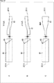
図1は、本技術を適用した積層レンズ構造体を用いたカメラモジュールの第1の実施の形態を示す図である。
<1. First Embodiment of Camera Module>
FIG. 1 is a diagram showing a first embodiment of a camera module using a laminated lens structure to which the present technology is applied.

図1のAは、カメラモジュール1の第1の実施の形態としてのカメラモジュール1Aの構成を示す模式図である。図1のBは、カメラモジュール1Aの概略断面図である。 FIG. 1A is a schematic view showing the configuration of the camera module 1A as the first embodiment of the camera module 1. FIG. 1B is a schematic cross-sectional view of the camera module 1A.

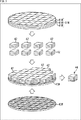
カメラモジュール1Aは、積層レンズ構造体11と受光素子12とを備える。積層レンズ構造体11は、縦横それぞれ5個ずつ、合計25個の光学ユニット13を備える。光学ユニット13は、1本の光軸方向に複数枚のレンズ21を含んで構成される。カメラモジュール1Aは、光学ユニット13を複数個備えた複眼カメラモジュールである。 The camera module 1A includes a laminated lens structure 11 and a light receiving element 12. The laminated lens structure 11 includes five optical units 13 in each of the vertical and horizontal directions, for a total of 25 optical units 13. The optical unit 13 includes a plurality of lenses 21 in the direction of one optical axis. The camera module 1A is a compound eye camera module including a plurality of optical units 13.

カメラモジュール1Aが備える複数個の光学ユニット13の光軸は、図1のBに示されるように、モジュールの外側に向かって広がるように配置され、これにより広角の画像の撮影が可能とされている。 As shown in FIG. 1B, the optical axes of the plurality of optical units 13 included in the camera module 1A are arranged so as to spread toward the outside of the module, which enables wide-angle image capture. There is.

なお、図1のBでは、簡単のため、積層レンズ構造体11はレンズ21を3層だけ積層した構造になっているが、より多くのレンズ21を積層して良いことは言うまでもない。 In addition, in B of FIG. 1, for the sake of simplicity, the laminated lens structure 11 has a structure in which only three layers of lenses 21 are laminated, but it goes without saying that more lenses 21 may be laminated.

図1のカメラモジュール1Aは、複数個の光学ユニット13を介して撮影した複数枚の画像をつなぎ合わせて、1枚の広角画像を作り出すことができる。複数枚の画像をつなぎ合わせるため、各画像を撮影する各光学ユニット13の形成および配置には、高い精度が要求される。また、特に広角側の光学ユニット13は、レンズ21への光の入射角度が小さいため、光学ユニット13の内での各レンズ21の位置関係と配置にも、高い精度が要求される。 The camera module 1A of FIG. 1 can create one wide-angle image by joining a plurality of images taken through a plurality of optical units 13. In order to join a plurality of images, high accuracy is required for the formation and arrangement of each optical unit 13 for capturing each image. Further, since the optical unit 13 on the wide-angle side has a small incident angle of light on the lens 21, high accuracy is required for the positional relationship and arrangement of each lens 21 in the optical unit 13.

図2は、特許文献1が開示する、樹脂による固着技術を用いた積層レンズ構造体の断面構造図である。 FIG. 2 is a cross-sectional structure diagram of a laminated lens structure using a resin fixing technique disclosed in Patent Document 1.

図2に示される積層レンズ構造体500においては、レンズ511を備えた基板512どうしを固着する手段として、樹脂513が用いられている。樹脂513は、UV硬化性などのエネルギー硬化性樹脂である。 In the laminated lens structure 500 shown in FIG. 2, resin 513 is used as a means for fixing the substrates 512 having the lens 511 to each other. Resin 513 is an energy curable resin such as UV curable.

基板512どうしを貼り合わせる前に、基板512表面全面に樹脂513の層が形成される。その後、基板512どうしが貼り合わされ、さらに、樹脂513が硬化される。これにより、貼り合わせた基板512どうしが固着される。 Before the substrates 512 are bonded to each other, a layer of resin 513 is formed on the entire surface of the substrates 512. After that, the substrates 512 are bonded to each other, and the resin 513 is further cured. As a result, the bonded substrates 512 are fixed to each other.

しかし、樹脂513を硬化させた際に、樹脂513は硬化収縮する。図2に示される構造の場合、基板512全体に樹脂513の層を形成した後、樹脂513を硬化させるため、樹脂513の変位量が大きくなってしまう。 However, when the resin 513 is cured, the resin 513 is cured and shrunk. In the case of the structure shown in FIG. 2, since the resin 513 is cured after the layer of the resin 513 is formed on the entire substrate 512, the displacement amount of the resin 513 becomes large.

また、基板512どうしを貼り合わせて形成した積層レンズ構造体500を個片化し、撮像素子を組み合わせてカメラモジュールを形成した後も、カメラモジュールに備わる積層レンズ構造体500は、図2に示されるように、レンズ511を備えた基板512間全体に、樹脂513が存在している。このため、カメラモジュールをカメラの筐体内に搭載し、実使用した際に、機器の発熱による温度上昇により、積層レンズ構造体500の基板間の樹脂が熱膨張する懸念がある。 Further, even after the laminated lens structure 500 formed by laminating the substrates 512 to each other is separated into individual pieces and the image pickup elements are combined to form the camera module, the laminated lens structure 500 provided in the camera module is shown in FIG. As described above, the resin 513 is present in the entire space between the substrates 512 provided with the lens 511. Therefore, when the camera module is mounted in the housing of the camera and actually used, there is a concern that the resin between the substrates of the laminated lens structure 500 may thermally expand due to the temperature rise due to the heat generated by the device.

図3は、図1のカメラモジュール1Aの積層レンズ構造体11のみを示した断面構造図である。 FIG. 3 is a cross-sectional structure diagram showing only the laminated lens structure 11 of the camera module 1A of FIG.

カメラモジュール1Aの積層レンズ構造体11も、レンズ21を備えたレンズ付き基板41を複数枚積層して形成されている。 The laminated lens structure 11 of the camera module 1A is also formed by laminating a plurality of lens-equipped substrates 41 having a lens 21.

カメラモジュール1Aの積層レンズ構造体11では、レンズ21を備えたレンズ付き基板41どうしを固定する手段として、図2の積層レンズ構造体500やその他の先行技術文献に示されるものとは全く異なる固定手段が用いられている。 In the laminated lens structure 11 of the camera module 1A, as a means for fixing the lens-equipped substrates 41 provided with the lens 21, the laminated lens structure 500 of FIG. 2 and other fixings completely different from those shown in the prior art documents are fixed. Means are used.

すなわち、積層される2枚のレンズ付き基板41は、一方の基板表面に形成した酸化物や窒化物による表面層と、他方の基板表面に形成した酸化物や窒化物による表面層と、の間の共有結合によって、直接接合される。具体例として、図4に示されるように、積層する2枚のレンズ付き基板41それぞれの表面に、表面層としてシリコン酸化膜もしくはシリコン窒化膜が形成され、これに水酸基を結合させた後、2枚のレンズ付き基板41どうしが貼り合わされ、昇温されて脱水縮合される。その結果、2枚のレンズ付き基板41の表面層の間で、シリコン−酸素共有結合が形成される。これにより2枚のレンズ付き基板41が直接接合される。なお、縮合の結果、2枚の表面層に含まれる元素同士が直接共有結合を形成することも起こり得る。 That is, the two laminated substrates 41 with lenses are between a surface layer made of oxides and nitrides formed on the surface of one substrate and a surface layer made of oxides and nitrides formed on the surface of the other substrate. It is directly joined by the covalent bond of. As a specific example, as shown in FIG. 4, a silicon oxide film or a silicon nitride film is formed as a surface layer on the surface of each of the two lens-equipped substrates 41 to be laminated, and after bonding a hydroxyl group to the silicon oxide film or silicon nitride film, 2 The substrates 41 with lenses are bonded to each other, heated to a high temperature, and dehydrated and condensed. As a result, a silicon-oxygen covalent bond is formed between the surface layers of the two lens-equipped substrates 41. As a result, the two substrates 41 with lenses are directly bonded. As a result of condensation, elements contained in the two surface layers may directly form a covalent bond.

本明細書では、このように、2枚のレンズ付き基板41の間に配置した無機物の層を介して2枚のレンズ付き基板41を固定すること、あるいは、2枚のレンズ付き基板41の表面にそれぞれ配置した無機物の層どうしを化学結合させることで2枚のレンズ付き基板41を固定すること、あるいは、2枚のレンズ付き基板41の表面にそれぞれ配置した無機物の層の間に脱水縮合による結合を形成することで2枚のレンズ付き基板41を固定すること、あるいは、2枚のレンズ付き基板41の表面にそれぞれ配置した無機物の層の間に、酸素を介した共有結合あるいは互いの無機物の層に含まれる元素どうしの共有結合を形成することで2枚のレンズ付き基板41を固定すること、あるいは、2枚のレンズ付き基板41の表面にそれぞれ配置したシリコン酸化物層もしくはシリコン窒化物層の間に、シリコン―酸素共有結合あるいはシリコン―シリコン共有結合を形成することで2枚のレンズ付き基板41を固定すること、を直接接合と呼ぶ。 In the present specification, the two lens-attached substrates 41 are fixed via the inorganic layer arranged between the two lens-attached substrates 41, or the surface of the two lens-attached substrates 41 is described. The two lens-equipped substrates 41 are fixed by chemically bonding the inorganic layers arranged in each of the above, or by dehydration condensation between the inorganic layers arranged on the surfaces of the two lens-equipped substrates 41. The two lens-equipped substrates 41 can be fixed by forming a bond, or covalent bonds or mutual inorganic substances can be covalently bonded between the layers of inorganic substances arranged on the surfaces of the two lens-equipped substrates 41, respectively. The two lens-equipped substrates 41 are fixed by forming a covalent bond between the elements contained in the layers, or the silicon oxide layer or silicon nitride arranged on the surface of the two lens-equipped substrates 41, respectively. Fixing two lens-attached substrates 41 by forming a silicon-oxygen covalent bond or a silicon-silicon covalent bond between layers is called a direct bond.

この貼り合わせと昇温による脱水縮合を行うため、本実施の形態では、半導体装置やフラットディスプレイ装置の製造分野で使用される基板を用いて、基板状態でレンズが形成され、基板状態で貼り合わせおよび昇温による脱水縮合が行われ、基板状態で共有結合による接合が行われる。2枚のレンズ付き基板41の表面に形成した無機物の層の間を、共有結合によって接合させた構造は、特許文献1が開示する図2で説明した技術を用いた場合に懸念される、基板全体に渡る樹脂513の硬化収縮による変形や、実使用時の樹脂513の熱膨張による変形を抑える、という作用または効果をもたらす。 In order to perform this bonding and dehydration condensation by raising the temperature, in the present embodiment, a lens is formed in the substrate state using a substrate used in the manufacturing field of semiconductor devices and flat display devices, and the lenses are bonded in the substrate state. Then, dehydration condensation is performed by raising the temperature, and bonding by covalent bonding is performed in the substrate state. The structure in which the layers of inorganic substances formed on the surfaces of the two lens-equipped substrates 41 are covalently bonded to each other is a substrate of concern when the technique described with reference to FIG. 2 disclosed in Patent Document 1 is used. It has the effect or effect of suppressing deformation due to curing shrinkage of the resin 513 and deformation due to thermal expansion of the resin 513 during actual use.

図5及び図6は、積層レンズ構造体11と受光素子12を組み合わせた図1のカメラモジュール1Aを形成する工程を示す図である。 5 and 6 are views showing a process of forming the camera module 1A of FIG. 1 in which the laminated lens structure 11 and the light receiving element 12 are combined.

まず、図5に示されるように、各レンズ21(不図示)が平面方向に複数形成されたレンズ付き基板41Wが複数枚用意され、これらが積層される。これにより、基板状態のレンズ付き基板41Wが複数枚積層された、基板状態の積層レンズ構造体11Wが得られる。 First, as shown in FIG. 5, a plurality of lens-attached substrates 41W in which a plurality of lenses 21 (not shown) are formed in the plane direction are prepared, and these are laminated. As a result, a laminated lens structure 11W in a substrate state is obtained in which a plurality of 41W substrates with lenses in the substrate state are laminated.

次に、図6に示されるように、受光素子12が平面方向に複数形成された基板状態のセンサ基板43Wが、図5に示した基板状態の積層レンズ構造体11Wとは別に作製され、用意される。 Next, as shown in FIG. 6, the sensor substrate 43W in the substrate state in which a plurality of light receiving elements 12 are formed in the plane direction is prepared separately from the laminated lens structure 11W in the substrate state shown in FIG. Will be done.

そして、基板状態のセンサ基板43Wと、基板状態の積層レンズ構造体11Wが、積層され、貼り合わせた基板のモジュール毎に外部端子を着けることで、基板状態のカメラモジュール44Wが得られる。 Then, the sensor substrate 43W in the substrate state and the laminated lens structure 11W in the substrate state are laminated, and an external terminal is attached to each module of the substrate in which the substrate state is attached, whereby the camera module 44W in the substrate state can be obtained.

最後に、基板状態のカメラモジュール44Wが、モジュール単位またはチップ単位に個片化される。個片化されたカメラモジュール44が、別途用意された筐体(不図示)に封入されることで、最終的なカメラモジュール44が得られる。 Finally, the camera module 44W in the board state is fragmented into module units or chip units. The individualized camera module 44 is enclosed in a separately prepared housing (not shown) to obtain the final camera module 44.

なお、本明細書及び図面においては、例えば、レンズ付き基板41Wのように、符号に“W”が付加された部品は、それが基板状態(ウエハ状態)であることを表し、レンズ付き基板41のように“W”が付されていないものは、モジュール単位またはチップ単位に個片化された状態であることを表す。その他、センサ基板43W、カメラモジュール44Wなどについても同様である。 In addition, in this specification and a drawing, for example, a component to which "W" is added to a code | symbol, such as a substrate 41W with a lens, indicates that it is a substrate state (wafer state), and the substrate 41 with a lens. Those without "W" such as "W" indicate that the lens is individualized in module units or chip units. The same applies to the sensor substrate 43W, the camera module 44W, and the like.

図7は、積層レンズ構造体11と受光素子12を組み合わせた図1のカメラモジュール1Aを形成する別の工程を示す図である。 FIG. 7 is a diagram showing another step of forming the camera module 1A of FIG. 1 in which the laminated lens structure 11 and the light receiving element 12 are combined.

まず、上述した工程と同様に、基板状態のレンズ付き基板41Wが複数枚積層された、基板状態の積層レンズ構造体11Wが製造される。 First, similarly to the above-described process, a laminated lens structure 11W in a substrate state is manufactured in which a plurality of substrates 41W with a lens in a substrate state are laminated.

次に、基板状態の積層レンズ構造体11Wが、個片化される。 Next, the laminated lens structure 11W in the substrate state is individualized.

また、基板状態の積層レンズ構造体11Wとは別に、基板状態のセンサ基板43Wが作製され、用意される。 Further, separately from the laminated lens structure 11W in the substrate state, a sensor substrate 43W in the substrate state is produced and prepared.

そして、基板状態のセンサ基板43Wの各受光素子12の上に、個片化された積層レンズ構造体11が1個ずつマウントされる。 Then, one individual laminated lens structure 11 is mounted on each light receiving element 12 of the sensor substrate 43W in the substrate state.

最後に、個片化された積層レンズ構造体11がマウントされた、基板状態のセンサ基板43Wがモジュール単位またはチップ単位に個片化される。積層レンズ構造体11がマウントされ、個片化されたセンサ基板43が、別途用意された筐体(不図示)に封入され、さらに外部端子が着けられることで、最終的なカメラモジュール44が得られる。 Finally, the sensor substrate 43W in the substrate state on which the individualized laminated lens structure 11 is mounted is individualized in module units or chip units. The laminated lens structure 11 is mounted, the individualized sensor substrate 43 is enclosed in a separately prepared housing (not shown), and an external terminal is attached to obtain the final camera module 44. Be done.

さらに、積層レンズ構造体11と受光素子12を組み合わせた図1のカメラモジュール1Aを形成する別の工程の例として、図7に示した基板状態のセンサ基板43Wを個片化し、その結果得られた個々の受光素子12へ、個片化後の積層レンズ構造体11をそれぞれマウントして、個片化されたカメラモジュール44を得ても良い。 Further, as an example of another step of forming the camera module 1A of FIG. 1 in which the laminated lens structure 11 and the light receiving element 12 are combined, the sensor substrate 43W in the substrate state shown in FIG. 7 is fragmented and obtained as a result. The laminated lens structure 11 after the individualization may be mounted on each of the individual light receiving elements 12 to obtain the individualized camera module 44.

図8は、カメラモジュール1Aにおけるレンズ付き基板41の構成を説明する図である。 FIG. 8 is a diagram illustrating a configuration of a substrate 41 with a lens in the camera module 1A.

図8のAは、図1のAと同様の、カメラモジュール1Aの構成を示す模式図である。 FIG. 8A is a schematic diagram showing the configuration of the camera module 1A similar to that of FIG. 1A.

図8のBは、図1のBと同様の、カメラモジュール1Aの概略断面図である。 FIG. 8B is a schematic cross-sectional view of the camera module 1A similar to FIG. 1B.

カメラモジュール1Aは、図8のBに示されるように、複数枚のレンズ21を組み合わせて形成し、1本の光軸を備えた光学ユニット13を、複数個備えた複眼カメラモジュールである。積層レンズ構造体11は、縦横それぞれ5個ずつ、合計25個の光学ユニット13を備える。 As shown in B of FIG. 8, the camera module 1A is a compound eye camera module formed by combining a plurality of lenses 21 and including a plurality of optical units 13 having one optical axis. The laminated lens structure 11 includes five optical units 13 in each of the vertical and horizontal directions, for a total of 25 optical units 13.

カメラモジュール1Aでは、複数個の光学ユニット13の光軸が、モジュールの外側に向かって広がるように配置され、これにより、広角の画像の撮影が可能とされている。図8のBでは、簡単のため、積層レンズ構造体11は、レンズ付き基板41を3層だけ積層した構造になっているが、より多くのレンズ付き基板41を積層して良いことは言うまでもない。 In the camera module 1A, the optical axes of the plurality of optical units 13 are arranged so as to spread toward the outside of the module, whereby a wide-angle image can be captured. In FIG. 8B, for the sake of simplicity, the laminated lens structure 11 has a structure in which only three layers of the lens-equipped substrates 41 are laminated, but it goes without saying that more lens-equipped substrates 41 may be laminated. ..

図8のC乃至Eは、積層レンズ構造体11を構成する3層のレンズ付き基板41それぞれの平面形状を示す図である。 C to E of FIG. 8 are views showing the planar shapes of the three-layer lens-attached substrates 41 constituting the laminated lens structure 11.

図8のCは、3層のうちの最上層のレンズ付き基板41の平面図であり、図8のDは、中層のレンズ付き基板41の平面図であり、図8のDは、最下層のレンズ付き基板41の平面図である。カメラモジュール1は、複眼広角カメラモジュールであるため、上層になるに従って、レンズ21の径が大きくなると共に、レンズ間のピッチが広がっている。 C in FIG. 8 is a plan view of the uppermost lens-equipped substrate 41 of the three layers, D in FIG. 8 is a plan view of the middle-layer lens-equipped substrate 41, and D in FIG. 8 is the lowest layer. It is a top view of the substrate 41 with a lens of. Since the camera module 1 is a compound-eye wide-angle camera module, the diameter of the lens 21 increases and the pitch between the lenses increases as the layer becomes higher.

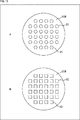
図8のF乃至Hは、図8のC乃至Eに示したレンズ付き基板41を得るための、基板状態のレンズ付き基板41Wの平面図である。 F to H in FIG. 8 are plan views of the lens-attached substrate 41W in the substrate state for obtaining the lens-attached substrate 41 shown in FIGS. 8C to E.

図8のFに示されるレンズ付き基板41Wは、図8のCのレンズ付き基板41に対応する基板状態を示し、図8のGに示されるレンズ付き基板41Wは、図8のDのレンズ付き基板41に対応する基板状態を示し、図8のHに示されるレンズ付き基板41Wは、図8のEのレンズ付き基板41に対応する基板状態を示している。 The lensed substrate 41W shown in F of FIG. 8 shows the substrate state corresponding to the lensed substrate 41 of C in FIG. 8, and the lensed substrate 41W shown in G of FIG. 8 has the lens of D in FIG. The substrate state corresponding to the substrate 41 is shown, and the lens-equipped substrate 41W shown in H of FIG. 8 shows the substrate state corresponding to the lens-attached substrate 41 of E of FIG.

図8のF乃至Hに示される基板状態のレンズ付き基板41Wは、図8のAに示したカメラモジュール1Aを、基板1枚につき8個得られる構成とされている。 The substrate 41W with a lens in the substrate state shown in F to H of FIG. 8 has a configuration in which eight camera modules 1A shown in A of FIG. 8 can be obtained for each substrate.

図8のF乃至Hの各レンズ付き基板41Wの間で、モジュール単位のレンズ付き基板41内のレンズ間のピッチは、上層のレンズ付き基板41Wと下層のレンズ付き基板41Wとで異なる一方、各レンズ付き基板41Wにおいて、モジュール単位のレンズ付き基板41を配置するピッチは、上層のレンズ付き基板41Wから下層のレンズ付き基板41Wまで、一定となっていることがわかる。 Among the lenses-equipped substrates 41W of F to H in FIG. 8, the pitch between the lenses in the lens-equipped substrate 41 for each module differs between the upper-layer lens-equipped substrate 41W and the lower-layer lens-equipped substrate 41W, while each of them. It can be seen that in the lens-equipped substrate 41W, the pitch at which the lens-equipped substrate 41 is arranged for each module is constant from the upper layer lens-equipped substrate 41W to the lower layer lens-equipped substrate 41W.

<2.カメラモジュールの第2の実施の形態>
図9は、本技術を適用した積層レンズ構造体を用いたカメラモジュールの第2の実施の形態を示す図である。
<2. Second Embodiment of the camera module>
FIG. 9 is a diagram showing a second embodiment of a camera module using a laminated lens structure to which the present technology is applied.

図9のAは、カメラモジュール1の第2の実施の形態としてのカメラモジュール1Bの外観を示す模式図である。図9のBは、カメラモジュール1Bの概略断面図である。 FIG. 9A is a schematic view showing the appearance of the camera module 1B as the second embodiment of the camera module 1. FIG. 9B is a schematic cross-sectional view of the camera module 1B.

カメラモジュール1Bは、2個の光学ユニット13を備える。2個の光学ユニット13は、積層レンズ構造体11の最上層に、絞り板51を備える。絞り板51には、開口部52が設けられている。 The camera module 1B includes two optical units 13. The two optical units 13 include a diaphragm plate 51 on the uppermost layer of the laminated lens structure 11. The aperture plate 51 is provided with an opening 52.

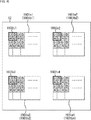
カメラモジュール1Bは2個の光学ユニット13を備えるが、これら2つの光学ユニット13の光学パラメータは異なる。すなわち、カメラモジュール1Bは、光学性能が異なる2種類の光学ユニット13を備える。2種類の光学ユニット13は、例えば、近景を撮影するための焦点距離が短い光学ユニット13と、遠景を撮影するために焦点距離が長い光学ユニット13とすることができる。 The camera module 1B includes two optical units 13, but the optical parameters of these two optical units 13 are different. That is, the camera module 1B includes two types of optical units 13 having different optical performances. The two types of optical units 13 can be, for example, an optical unit 13 having a short focal length for photographing a near view and an optical unit 13 having a long focal length for photographing a distant view.

カメラモジュール1Bでは、2つの光学ユニット13の光学パラメータが異なるため、例えば、図9のBに示されように、2つの光学ユニット13のレンズ21の枚数が異なる。また、2つの光学ユニット13が備える積層レンズ構造体11の同じ層のレンズ21において、径、厚さ、表面形状、体積、または、隣接するレンズとの距離、のいずれかが異なる構成が可能となっている。このため、カメラモジュール1Bにおけるレンズ21の平面形状は、例えば、図9のCに示されるように、2つの光学ユニット13が同じ径のレンズ21を備えていても良いし、図9のDに示すように、
異なる形状のレンズ21を備えていても良いし、図9のEに示すように、一方がレンズ21を備えない空洞21Xとなった構造でも良い。
In the camera module 1B, since the optical parameters of the two optical units 13 are different, for example, as shown in B of FIG. 9, the number of lenses 21 of the two optical units 13 is different. Further, the lenses 21 having the same layer of the laminated lens structure 11 included in the two optical units 13 can be configured to have different diameters, thicknesses, surface shapes, volumes, or distances from adjacent lenses. It has become. Therefore, as for the planar shape of the lens 21 in the camera module 1B, for example, as shown in C of FIG. 9, the two optical units 13 may have the lens 21 having the same diameter, and in D of FIG. As shown,
Lenses 21 having different shapes may be provided, or as shown in E of FIG. 9, one of them may have a hollow 21X structure without the lens 21.

図9のF乃至Hは、図9のC乃至Eに示したレンズ付き基板41を得るための、基板状態のレンズ付き基板41Wの平面図である。 F to H in FIG. 9 are plan views of the lens-attached substrate 41W in the substrate state for obtaining the lens-attached substrate 41 shown in FIGS. 9C to E.

図9のFに示されるレンズ付き基板41Wは、図9のCのレンズ付き基板41に対応する基板状態を示し、図9のGに示されるレンズ付き基板41Wは、図9のDのレンズ付き基板41に対応する基板状態を示し、図9のHに示されるレンズ付き基板41Wは、図9のEのレンズ付き基板41に対応する基板状態を示している。 The lensed substrate 41W shown in F of FIG. 9 shows the substrate state corresponding to the lensed substrate 41 of C in FIG. 9, and the lensed substrate 41W shown in G of FIG. 9 has the lens of D in FIG. The substrate state corresponding to the substrate 41 is shown, and the lens-equipped substrate 41W shown in H of FIG. 9 shows the substrate state corresponding to the lens-equipped substrate 41 of E of FIG.

図9のF乃至Hに示される基板状態のレンズ付き基板41Wは、図9のAに示したカメラモジュール1Bを、基板1枚につき16個得られる構成とされている。 The lens-attached substrate 41W in the substrate state shown in F to H of FIG. 9 has a configuration in which 16 camera modules 1B shown in A of FIG. 9 can be obtained for each substrate.

図9のF乃至Hに示されるように、カメラモジュール1Bを形成するために、基板状態のレンズ付き基板41Wの基板全面に同じ形状のレンズを形成することや、異なる形状のレンズを形成することや、レンズを形成したり形成しなかったりすることが可能である。 As shown in F to H of FIG. 9, in order to form the camera module 1B, a lens having the same shape or a lens having a different shape is formed on the entire surface of the substrate 41W with a lens in the substrate state. Or, it is possible to form or not form a lens.

<3.カメラモジュールの第3の実施の形態>
図10は、本技術を適用した積層レンズ構造体を用いたカメラモジュールの第3の実施の形態を示す図である。
<3. Third Embodiment of the camera module>
FIG. 10 is a diagram showing a third embodiment of a camera module using a laminated lens structure to which the present technology is applied.

図10のAは、カメラモジュール1の第3の実施の形態としてのカメラモジュール1Cの外観を示す模式図である。図10のBは、カメラモジュール1Cの概略断面図である。 FIG. 10A is a schematic view showing the appearance of the camera module 1C as the third embodiment of the camera module 1. FIG. 10B is a schematic cross-sectional view of the camera module 1C.

カメラモジュール1Cは、光の入射面上に、縦横2個ずつ、合計4個の光学ユニット13を備える。4個の光学ユニット13どうしでは、レンズ21の形状は同じになっている。 The camera module 1C includes a total of four optical units 13 on the incident surface of light, two in each of the vertical and horizontal directions. The shape of the lens 21 is the same among the four optical units 13.

4個の光学ユニット13は、積層レンズ構造体11の最上層に、絞り板51を備えるが、その絞り板51の開口部52の大きさが、4個の光学ユニット13の間で異なる。これにより、カメラモジュール1Cは、例えば、以下のようなカメラモジュール1Cを実現することができる。すなわち、例えば防犯用の監視カメラにおいて、昼間のカラー画像監視用に、RGB3種類のカラーフィルタを備えてRGB3種の光を受光する受光画素と、夜間の白黒画像監視用に、RGB用のカラーフィルタを備えない受光画素と、を備えた受光素子12を用いたカメラモジュール1Cにおいて、照度が低い夜間の白黒画像を撮影するための画素だけ絞りの開口の大きさを大きくすることが可能となる。このため、1個のカメラモジュール1Cにおけるレンズ21の平面形状は、例えば図10のCに示されるように、4つの光学ユニット13が備えるレンズ21の径は同じであって、かつ、図10のDに示されるように、絞り板51の開口部52の大きさは、光学ユニット13によっては異なる。 The four optical units 13 include a diaphragm plate 51 on the uppermost layer of the laminated lens structure 11, but the size of the opening 52 of the diaphragm plate 51 differs among the four optical units 13. Thereby, the camera module 1C can realize, for example, the following camera module 1C. That is, for example, in a security surveillance camera, a light receiving pixel equipped with RGB 3 types of color filters for daytime color image monitoring and receiving RGB 3 types of light, and an RGB color filter for nighttime black and white image monitoring. In the camera module 1C using the light receiving pixel not provided with the light receiving pixel and the light receiving element 12 provided with the light receiving pixel, it is possible to increase the size of the aperture of the aperture by only the pixel for capturing a black and white image at night when the illumination is low. Therefore, the planar shape of the lens 21 in one camera module 1C has the same diameter of the lens 21 included in the four optical units 13 as shown in C of FIG. 10, for example, and the diameter of the lens 21 included in FIG. 10 is the same. As shown in D, the size of the opening 52 of the aperture plate 51 differs depending on the optical unit 13.

図10のEは、図10のCに示したレンズ付き基板41を得るための、基板状態のレンズ付き基板41Wの平面図である。図10のFは、図10のDに示した絞り板51を得るための、基板状態での絞り板51Wを示す平面図である。 FIG. 10E is a plan view of the lens-equipped substrate 41W in the substrate state for obtaining the lens-equipped substrate 41 shown in FIG. 10C. FIG. 10F is a plan view showing the diaphragm plate 51W in the substrate state for obtaining the diaphragm plate 51 shown in FIG. 10D.

図10のEの基板状態のレンズ付き基板41W、及び、図10のFの基板状態の絞り板51Wでは、図10のAに示したカメラモジュール1Cを、基板1枚につき8個得られる構成とされている。 In the substrate 41W with a lens in the substrate state of E in FIG. 10 and the diaphragm plate 51W in the substrate state of F in FIG. 10, eight camera modules 1C shown in A of FIG. 10 can be obtained for each substrate. Has been done.

図10のFに示されるように、基板状態での絞り板51Wでは、カメラモジュール1Cを形成するために、カメラモジュール1Cが備える光学ユニット13毎に、異なる開口部52の大きさを設定することができる。 As shown in F of FIG. 10, in the aperture plate 51W in the substrate state, in order to form the camera module 1C, a different size of the opening 52 is set for each optical unit 13 included in the camera module 1C. Can be done.

<4.カメラモジュールの第4の実施の形態>
図11は、本技術を適用した積層レンズ構造体を用いたカメラモジュールの第4の実施の形態を示す図である。
<4. Fourth Embodiment of Camera Module>
FIG. 11 is a diagram showing a fourth embodiment of a camera module using a laminated lens structure to which the present technology is applied.

図11のAは、カメラモジュール1の第4の実施の形態としてのカメラモジュール1Dの外観を示す模式図である。図11のBは、カメラモジュール1Dの概略断面図である。 FIG. 11A is a schematic view showing the appearance of the camera module 1D as the fourth embodiment of the camera module 1. FIG. 11B is a schematic cross-sectional view of the camera module 1D.

カメラモジュール1Dは、カメラモジュール1Cと同様に、光の入射面上に、縦横2個ずつ、合計4個の光学ユニット13を備える。4個の光学ユニット13どうしでは、レンズ21の形状と絞り板51の開口部52の大きさは同じになっている。 Similar to the camera module 1C, the camera module 1D includes two optical units 13 in each of the vertical and horizontal directions on the incident surface of light, for a total of four optical units 13. In the four optical units 13, the shape of the lens 21 and the size of the opening 52 of the aperture plate 51 are the same.

カメラモジュール1Dは、光の入射面の縦方向と横方向のそれぞれについて2個ずつ配置した光学ユニット13に備わる光軸が、同じ方向に延びている。図11のBに示される1点鎖線は、光学ユニット13それぞれの光軸を表している。この様な構造のカメラモジュール1Dは、超解像技術を利用して、1個の光学ユニット13で撮影するよりも、解像度が高い画像を撮影することに適している。 In the camera module 1D, two optical axes are arranged in each of the vertical direction and the horizontal direction of the incident surface of light, and the optical axes provided in the optical units 13 extend in the same direction. The alternate long and short dash line shown in B of FIG. 11 represents the optical axis of each of the optical units 13. The camera module 1D having such a structure is suitable for taking an image having a higher resolution than taking a picture with one optical unit 13 by using super-resolution technology.

カメラモジュール1Dでは、縦方向と横方向のそれぞれについて、光軸が同じ方向を向きながら、異なる位置に配置された複数個の受光素子12で画像を撮影することにより、あるいは1個の受光素子12の中の異なる領域の受光画素で画像を撮影することにより、光軸が同じ方向を向きながら、必ずしも同一ではない複数枚の画像を得ることができる。これら同一ではない複数枚の画像が持っている場所毎の画像データを合わせることで、解像度が高い画像を得ることができる。このため、1個カメラモジュール1Dにおけるレンズ21の平面形状は、図11のCに示されるように、4つの光学ユニット13で同じになっていることが望ましい。 In the camera module 1D, images are taken by a plurality of light receiving elements 12 arranged at different positions while the optical axes are oriented in the same direction in each of the vertical direction and the horizontal direction, or one light receiving element 12 is used. By taking images with light receiving pixels in different regions of the inside, it is possible to obtain a plurality of images that are not necessarily the same while the optical axes are oriented in the same direction. An image with high resolution can be obtained by combining the image data for each location held by a plurality of images that are not the same. Therefore, it is desirable that the planar shape of the lens 21 in the one camera module 1D is the same for the four optical units 13 as shown in FIG. 11C.

図11のDは、図11のCに示したレンズ付き基板41を得るための、基板状態のレンズ付き基板41Wの平面図である。基板状態のレンズ付き基板41Wは、図11のAに示したカメラモジュール1Dを、基板1枚につき8個得られる構成とされている。 FIG. 11D is a plan view of the lens-equipped substrate 41W in the substrate state for obtaining the lens-equipped substrate 41 shown in FIG. 11C. The substrate 41W with a lens in the substrate state has a configuration in which eight camera modules 1D shown in FIG. 11A can be obtained for each substrate.

図11のDに示されるように、基板状態のレンズ付き基板41Wでは、カメラモジュール1Dを形成するために、カメラモジュール1Dが複数個のレンズ21を備え、この1個のモジュール用のレンズ群が、基板上に一定のピッチで複数個配置されている。 As shown in D of FIG. 11, in the substrate 41W with a lens in the substrate state, the camera module 1D includes a plurality of lenses 21 in order to form the camera module 1D, and the lens group for this one module is provided. , A plurality of them are arranged on the substrate at a constant pitch.

<5.カメラモジュールの第5の実施の形態>
図12は、本技術を適用した積層レンズ構造体を用いたカメラモジュールの第5の実施の形態を示す図である。
<5. Fifth Embodiment of Camera Module>
FIG. 12 is a diagram showing a fifth embodiment of a camera module using a laminated lens structure to which the present technology is applied.

図12のAは、カメラモジュール1の第5の実施の形態としてのカメラモジュール1Eの外観を示す模式図である。図12のBは、カメラモジュール1Eの概略断面図である。 FIG. 12A is a schematic view showing the appearance of the camera module 1E as the fifth embodiment of the camera module 1. FIG. 12B is a schematic cross-sectional view of the camera module 1E.

カメラモジュール1Eは、1本の光軸を有する光学ユニット13をカメラモジュール1E内に1個備える、単眼のカメラモジュールである。 The camera module 1E is a monocular camera module including one optical unit 13 having one optical axis in the camera module 1E.

図12のCは、カメラモジュール1Eにおけるレンズ21の平面形状を示すレンズ付き基板41の平面図である。カメラモジュール1Eは、1個の光学ユニット13を備える。 FIG. 12C is a plan view of the lens-equipped substrate 41 showing the plan shape of the lens 21 in the camera module 1E. The camera module 1E includes one optical unit 13.

図12のDは、図12のCに示したレンズ付き基板41を得るための、基板状態のレンズ付き基板41Wの平面図である。基板状態のレンズ付き基板41Wは、図12のAに示したカメラモジュール1Eを、基板1枚につき32個得られる構成とされている。 FIG. 12D is a plan view of the lens-equipped substrate 41W in the substrate state for obtaining the lens-equipped substrate 41 shown in FIG. 12C. The substrate 41W with a lens in the substrate state has a configuration in which 32 camera modules 1E shown in FIG. 12A can be obtained for each substrate.

図12のDに示されるように、基板状態のレンズ付き基板41Wでは、カメラモジュール1E用のレンズ21が、基板上に一定のピッチで複数個配置されている。 As shown in D of FIG. 12, in the substrate 41W with a lens in the substrate state, a plurality of lenses 21 for the camera module 1E are arranged on the substrate at a constant pitch.

<6.第4の実施の形態のカメラモジュールの詳細構成>
次に、図13を参照して、図11に示した第4の実施の形態に係るカメラモジュール1Dの詳細構成について説明する。
<6. Detailed configuration of the camera module of the fourth embodiment>
Next, with reference to FIG. 13, the detailed configuration of the camera module 1D according to the fourth embodiment shown in FIG. 11 will be described.

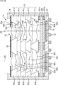
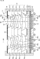
図13は、図11のBに示したカメラモジュール1Dの断面図である。 FIG. 13 is a cross-sectional view of the camera module 1D shown in FIG. 11B.

カメラモジュール1Dは、複数のレンズ付き基板41a乃至41eが積層された積層レンズ構造体11と、受光素子12を含んで構成される。積層レンズ構造体11は、
複数個の光学ユニット13を備える。1点鎖線84は、それぞれの光学ユニット13の光軸を表す。受光素子12は、積層レンズ構造体11の下側に配置されている。カメラモジュール1Dにおいて、上方からカメラモジュール1D内へと入射した光は、積層レンズ構造体11を透過し、積層レンズ構造体11の下側に配置された受光素子12で受光される。
The camera module 1D includes a laminated lens structure 11 in which a plurality of lens-attached substrates 41a to 41e are laminated, and a light receiving element 12. The laminated lens structure 11 is
A plurality of optical units 13 are provided. The alternate long and short dash line 84 represents the optical axis of each optical unit 13. The light receiving element 12 is arranged below the laminated lens structure 11. In the camera module 1D, the light incident on the camera module 1D from above passes through the laminated lens structure 11 and is received by the light receiving element 12 arranged under the laminated lens structure 11.

積層レンズ構造体11は、積層された5枚のレンズ付き基板41a乃至41eを備える。5枚のレンズ付き基板41a乃至41eを特に区別しない場合には、単に、レンズ付き基板41と記述して説明する。 The laminated lens structure 11 includes five laminated substrates 41a to 41e with lenses. When the five lens-attached substrates 41a to 41e are not particularly distinguished, the description will be simply described as the lens-attached substrate 41.

積層レンズ構造体11を構成する各レンズ付き基板41の貫通孔83の断面形状は、下側(受光素子12を配置する側)に向かって開口幅が小さくなる、いわゆる下すぼみの形状となっている The cross-sectional shape of the through hole 83 of each lens-equipped substrate 41 constituting the laminated lens structure 11 has a so-called downward recess shape in which the opening width decreases toward the lower side (the side on which the light receiving element 12 is arranged). Is

積層レンズ構造体11の上には、絞り板51が配置されている。絞り板51は、例えば、光吸収性もしくは遮光性を有する材料で形成された層を備える。絞り板51には、開口部52が設けられている。 A diaphragm plate 51 is arranged on the laminated lens structure 11. The diaphragm plate 51 includes, for example, a layer made of a material having a light absorbing property or a light blocking property. The aperture plate 51 is provided with an opening 52.

受光素子12は、例えば、表面照射型または裏面照射型のCMOS(Complementary Metal Oxide Semiconductor)イメージセンサで構成される。受光素子12の積層レンズ構造体11側となる上側の面には、オンチップレンズ71が形成されており、受光素子12の下側の面には、信号を入出力する外部端子72が形成されている。 The light receiving element 12 is composed of, for example, a front-illuminated or back-illuminated CMOS (Complementary Metal Oxide Semiconductor) image sensor. An on-chip lens 71 is formed on the upper surface of the light receiving element 12 on the laminated lens structure 11 side, and an external terminal 72 for inputting / outputting signals is formed on the lower surface of the light receiving element 12. ing.

積層レンズ構造体11、受光素子12、絞り板51などは、レンズバレル74に収納されている。 The laminated lens structure 11, the light receiving element 12, the diaphragm plate 51, and the like are housed in the lens barrel 74.

受光素子12の上側には、構造材73が配置されている。その構造材73を介して、積層レンズ構造体11と受光素子12とが固定されている。構造材73は、例えばエポキシ系の樹脂である。 A structural material 73 is arranged on the upper side of the light receiving element 12. The laminated lens structure 11 and the light receiving element 12 are fixed via the structural material 73. The structural material 73 is, for example, an epoxy-based resin.

本実施の形態では、積層レンズ構造体11は、積層された5枚のレンズ付き基板41a乃至41eを備えるが、レンズ付き基板41の積層枚数は2枚以上であれば特に限定されない。 In the present embodiment, the laminated lens structure 11 includes five laminated substrates 41a to 41e with lenses, but the number of laminated substrates 41 with lenses is not particularly limited as long as it is two or more.

積層レンズ構造体11を構成するそれぞれのレンズ付き基板41は、担体基板81にレンズ樹脂部82が追加された構成である。担体基板81は貫通孔83を有し、貫通孔83の内側に、レンズ樹脂部82が形成されている。レンズ樹脂部82は、上述したレンズ21を含み、担体基板81まで延在してレンズ21を担持する部位も併せて、レンズ21を構成する材料によって一体となった部分を表す。 Each of the lens-attached substrates 41 constituting the laminated lens structure 11 has a configuration in which a lens resin portion 82 is added to the carrier substrate 81. The carrier substrate 81 has a through hole 83, and a lens resin portion 82 is formed inside the through hole 83. The lens resin portion 82 includes the above-mentioned lens 21, and also includes a portion extending to the carrier substrate 81 to support the lens 21 and represents a portion integrated with the material constituting the lens 21.

なお、レンズ付き基板41a乃至41eそれぞれの担体基板81、レンズ樹脂部82、または、貫通孔83を区別する場合には、図13に示されるように、レンズ付き基板41a乃至41eに対応して、担体基板81a乃至81e、レンズ樹脂部82a乃至82e、または、貫通孔83a乃至83eのように記述して説明する。 When distinguishing the carrier substrate 81, the lens resin portion 82, or the through hole 83 of each of the lens-attached substrates 41a to 41e, as shown in FIG. 13, the lens-attached substrates 41a to 41e correspond to the lens-attached substrates 41a to 41e. The description will be described as the carrier substrates 81a to 81e, the lens resin portions 82a to 82e, or the through holes 83a to 83e.

<レンズ樹脂部の詳細説明>
次に、レンズ付き基板41aのレンズ樹脂部82aを例に、レンズ樹脂部82の形状について説明する。
<Detailed explanation of the lens resin part>
Next, the shape of the lens resin portion 82 will be described by taking the lens resin portion 82a of the substrate 41a with a lens as an example.

図14は、レンズ付き基板41aを構成する担体基板81aとレンズ樹脂部82aの平面図と断面図である。 FIG. 14 is a plan view and a cross-sectional view of the carrier substrate 81a and the lens resin portion 82a constituting the lens-attached substrate 41a.

図14に示される担体基板81aとレンズ樹脂部82aの断面図は、平面図に示されているB‐B’線とC‐C’線の断面図である。 The cross-sectional view of the carrier substrate 81a and the lens resin portion 82a shown in FIG. 14 is a cross-sectional view of lines BB'and C-C'shown in the plan view.

レンズ樹脂部82aは、レンズ21を構成する材料によって一体となって形成した部位であり、レンズ部91と担持部92を備える。上述した説明において、レンズ21とは、レンズ部91またはレンズ樹脂部82a全体に相当する。 The lens resin portion 82a is a portion integrally formed of materials constituting the lens 21, and includes a lens portion 91 and a supporting portion 92. In the above description, the lens 21 corresponds to the lens portion 91 or the entire lens resin portion 82a.

レンズ部91は、レンズとしての性能を有する部位、言い換えれば、「光を屈折させて集束もしくは発散させる部位」、あるいは、「凸面や凹面や非球面などの曲面を備えた部位、もしくはフレネルレンズや回折格子を利用したレンズで用いる複数個の多角形を連続して配置した部位」である。 The lens unit 91 is a portion having a performance as a lens, in other words, a "portion that refracts light to focus or diverge", or a "portion having a curved surface such as a convex surface, a concave surface, or an aspherical surface, or a Fresnel lens. This is a portion in which a plurality of polygons used in a lens using a diffraction grating are continuously arranged.

担持部92は、レンズ部91から担体基板81aまで延在してレンズ部91を担持する部位である。担持部92は、腕部101と脚部102で構成され、レンズ部91の外周に位置する。 The supporting portion 92 is a portion extending from the lens portion 91 to the carrier substrate 81a to support the lens portion 91. The supporting portion 92 is composed of an arm portion 101 and a leg portion 102, and is located on the outer periphery of the lens portion 91.

腕部101は、レンズ部91の外側に、レンズ部91に接して配置し、レンズ部91から外側方向へ一定の膜厚で延在する部位である。脚部102は、担持部92のなかで腕部101以外の部分で、かつ貫通孔83aの側壁に接する部分を含む部位である。脚部102は、腕部101よりも樹脂の膜厚が厚いことが好ましい。 The arm portion 101 is arranged outside the lens portion 91 in contact with the lens portion 91, and extends outward from the lens portion 91 with a constant film thickness. The leg portion 102 is a portion of the supported portion 92 other than the arm portion 101 and includes a portion in contact with the side wall of the through hole 83a. It is preferable that the leg portion 102 has a thicker resin film thickness than the arm portion 101.

担体基板81aに形成された貫通孔83aの平面形状は円形であり、その断面形状は当然直径の方向によらず同じである。レンズ形成時に上型と下型の形によって決まる形状であるレンズ樹脂部82aの形状も、その断面形状が直径の方向によらず同じとなるように形成されている。 The planar shape of the through hole 83a formed in the carrier substrate 81a is circular, and the cross-sectional shape thereof is naturally the same regardless of the direction of the diameter. The shape of the lens resin portion 82a, which is a shape determined by the shapes of the upper mold and the lower mold when the lens is formed, is also formed so that the cross-sectional shape is the same regardless of the direction of the diameter.

図15は、図13のカメラモジュール1Dの一部である積層レンズ構造体11と絞り板51を示す断面図である。 FIG. 15 is a cross-sectional view showing a laminated lens structure 11 and an aperture plate 51 which are a part of the camera module 1D of FIG.

カメラモジュール1Dでは、モジュールに入射される光が絞り板51で絞られた後、積層レンズ構造体11の内部で広げられて、積層レンズ構造体11の下方に配置された受光素子12(図15では不図示)へと入射される。すなわち、積層レンズ構造体11全体について概観すると、モジュールに入射された光は、絞り板51の開口部52から下側に向かって、ほぼ末広がりに広がって進行する。このため、積層レンズ構造体11に備わるレンズ樹脂部82の大きさの一例として、図15の積層レンズ構造体11においては、絞り板51の直下に配置されたレンズ付き基板41aに備わるレンズ樹脂部82aが最も小さく、積層レンズ構造体11の最下層に配置されたレンズ付き基板41eに備わるレンズ樹脂部82eが最も大きくなっている。 In the camera module 1D, the light incident on the module is focused by the diaphragm plate 51, then spread inside the laminated lens structure 11 and arranged below the laminated lens structure 11 (FIG. 15). (Not shown). That is, when the entire laminated lens structure 11 is reviewed, the light incident on the module spreads and travels substantially toward the lower side from the opening 52 of the diaphragm plate 51. Therefore, as an example of the size of the lens resin portion 82 provided in the laminated lens structure 11, in the laminated lens structure 11 of FIG. 15, the lens resin portion provided in the lens-equipped substrate 41a arranged directly under the aperture plate 51. 82a is the smallest, and the lens resin portion 82e provided on the lens-equipped substrate 41e arranged at the bottom layer of the laminated lens structure 11 is the largest.

仮にレンズ付き基板41のレンズ樹脂部82の厚さを一定にした場合、大きさが小さなレンズよりも大きなレンズを作る方が難しい。それは例えば、レンズを製造する際にレンズに加わる荷重によってレンズが変形しやすい、大きさが大きいゆえに強度を保つのが難しい、との理由による。このため、大きさが大きなレンズは、大きさが小さなレンズよりも、厚さを厚くすることが好ましい。このため、図15の積層レンズ構造体11においては、レンズ樹脂部82の厚さは、最下層に配置したレンズ付き基板41eに備わるレンズ樹脂部82eが最も厚くなっている。 If the thickness of the lens resin portion 82 of the substrate 41 with a lens is made constant, it is more difficult to make a lens having a larger size than a lens having a smaller size. This is because, for example, the lens is easily deformed by the load applied to the lens when the lens is manufactured, and it is difficult to maintain the strength due to its large size. For this reason, it is preferable that a lens having a large size has a larger thickness than a lens having a small size. Therefore, in the laminated lens structure 11 of FIG. 15, the thickness of the lens resin portion 82 is the thickest in the lens resin portion 82e provided in the lens-attached substrate 41e arranged in the lowermost layer.

図15の積層レンズ構造体11は、レンズ設計の自由度を高めるために、さらに以下の特徴の少なくとも一つを備える。
(1) 担体基板81の厚さが、積層レンズ構造体11を構成する少なくとも複数枚のレンズ付き基板41の間で異なる。例えば、担体基板81の厚さが、下層のレンズ付き基板41の方が厚い。
(2) レンズ付き基板41に備わる貫通孔83の開口幅が、積層レンズ構造体11を構成する少なくとも複数枚のレンズ付き基板41の間で異なる。例えば、貫通孔83の開口幅が、下層のレンズ付き基板41の方が大きい。
(3) レンズ付き基板41に備わるレンズ部91の直径が、積層レンズ構造体11を構成する少なくとも複数枚のレンズ付き基板41の間で異なる。例えば、レンズ部91の直径が、下層のレンズ付き基板41のレンズ部91の方が大きい。
(4) レンズ付き基板41に備わるレンズ部91の厚さが、積層レンズ構造体11を構成する少なくとも複数枚のレンズ付き基板41の間で異なる。例えば、レンズ部91の厚さが、下層のレンズ付き基板41のレンズ部91の方が厚い。
(5) レンズ付き基板41に備わるレンズ間の距離が、積層レンズ構造体11を構成する少なくとも複数枚のレンズ付き基板41の間で異なる。
(6) レンズ付き基板41に備わるレンズ樹脂部82の体積が、積層レンズ構造体11を構成する少なくとも複数枚のレンズ付き基板41の間で、異なる。例えば、レンズ樹脂部82の体積が、下層のレンズ付き基板41のレンズ樹脂部82の方が大きい。
(7) レンズ付き基板41に備わるレンズ樹脂部82の材料が、積層レンズ構造体11を構成する少なくとも複数枚のレンズ付き基板41の間で異なる。
The laminated lens structure 11 of FIG. 15 further includes at least one of the following features in order to increase the degree of freedom in lens design.
(1) The thickness of the carrier substrate 81 differs among at least a plurality of lens-attached substrates 41 constituting the laminated lens structure 11. For example, the thickness of the carrier substrate 81 is thicker in the lower layer substrate 41 with a lens.
(2) The opening width of the through hole 83 provided in the lens-equipped substrate 41 differs between at least a plurality of lens-equipped substrates 41 constituting the laminated lens structure 11. For example, the opening width of the through hole 83 is larger in the lower layer lens-attached substrate 41.
(3) The diameter of the lens portion 91 provided on the lens-attached substrate 41 differs between at least a plurality of lens-attached substrates 41 constituting the laminated lens structure 11. For example, the diameter of the lens portion 91 is larger in the lens portion 91 of the lower layer substrate 41 with a lens.
(4) The thickness of the lens portion 91 provided on the lens-attached substrate 41 differs between at least a plurality of lens-attached substrates 41 constituting the laminated lens structure 11. For example, the thickness of the lens portion 91 is thicker in the lens portion 91 of the lower layer substrate 41 with a lens.
(5) The distance between the lenses provided on the lens-equipped substrate 41 differs between at least a plurality of lens-equipped substrates 41 constituting the laminated lens structure 11.
(6) The volume of the lens resin portion 82 provided on the lens-attached substrate 41 differs between at least a plurality of lens-attached substrates 41 constituting the laminated lens structure 11. For example, the volume of the lens resin portion 82 is larger in the lens resin portion 82 of the lower layer lens-attached substrate 41.
(7) The material of the lens resin portion 82 provided on the lens-attached substrate 41 is different among at least a plurality of lens-attached substrates 41 constituting the laminated lens structure 11.

一般的に、カメラモジュールに入射される入射光は、垂直入射光と射入射光とを併せて含んでいる。射入射光の多くは絞り板51に当たり、そこで吸収もしくはカメラモジュール1Dの外側へ反射される。絞り板51によって絞りきれなかった射入射光は、その入射角度によっては貫通孔83の側壁に当たってしまい、そこで反射される可能性がある。 Generally, the incident light incident on the camera module includes both the vertically incident light and the emitted incident light. Most of the emitted and incident light hits the diaphragm plate 51, where it is absorbed or reflected to the outside of the camera module 1D. Depending on the angle of incidence, the emitted incident light that cannot be narrowed down by the diaphragm plate 51 may hit the side wall of the through hole 83 and be reflected there.

射入射光の反射光が進行する方向は、図13において示される、射入射光85の入射角度と、貫通孔83の側壁の角度とによって決まる。貫通孔83の開口幅が、入射側から受光素子12側へ向かって大きくなる、いわゆる、末広がりの形状の場合、絞り板51によって絞りきれなかった特定の入射角度の射入射光85が、貫通孔83の側壁に当たってしまった際には、それが受光素子12方向へと反射されてしまい、これが迷光あるいはノイズ光となる可能性がある。 The direction in which the reflected light of the emitted incident light travels is determined by the incident angle of the emitted incident light 85 and the angle of the side wall of the through hole 83 shown in FIG. In the case of a so-called divergent shape in which the opening width of the through hole 83 increases from the incident side toward the light receiving element 12, the emitted incident light 85 at a specific incident angle that cannot be narrowed down by the diaphragm plate 51 is the through hole. When it hits the side wall of 83, it is reflected in the direction of the light receiving element 12, which may become stray light or noise light.

しかしながら、図13に示した積層レンズ構造体11においては、図15に示されるように、貫通孔83は、下側(受光素子12を配置する側)に向かって開口幅が小さくなる、いわゆる下すぼみの形状となっている。この形状の場合、貫通孔83の側壁に当たった射入射光85は、下側方向いわゆる受光素子12の方向ではなく、上側方向、いわゆる入射側方向へと反射される。これにより、迷光あるいはノイズ光の発生を抑えるという作用または効果が得られる。 However, in the laminated lens structure 11 shown in FIG. 13, as shown in FIG. 15, the through hole 83 has a so-called lower opening width that becomes smaller toward the lower side (the side on which the light receiving element 12 is arranged). It has a dented shape. In the case of this shape, the emitted incident light 85 that hits the side wall of the through hole 83 is reflected not in the downward direction, that is, in the direction of the light receiving element 12, but in the upward direction, that is, in the so-called incident side direction. As a result, the action or effect of suppressing the generation of stray light or noise light can be obtained.

レンズ付き基板41の貫通孔83は、その側壁に当たって反射される光を低減するために、光吸収性の材料を側壁に配置するとなお良い。 It is more preferable that the through hole 83 of the substrate 41 with a lens has a light absorbing material arranged on the side wall in order to reduce the light reflected by the side wall thereof.

一例として、カメラモジュール1Dをカメラとして使用する際に受光したい波長の光(例えば可視光)を、第1の光とし、その第1の光とは波長が異なる光(例えばUV光)を、第2の光とした場合、第2の光(UV光)によって硬化する樹脂に、第1の光(可視光)の吸収材料としてカーボン粒子を分散させたものを、担体基板81の表面に塗布または噴射し、貫通孔83の側壁部の樹脂のみに第2の光(UV光)を照射して硬化させ、これ以外の領域の樹脂を除去することで、貫通孔83の側壁に、第1の光(可視光)に対する光吸収性を有する材料の層を形成して良い。 As an example, when the camera module 1D is used as a camera, light having a wavelength to be received (for example, visible light) is set as the first light, and light having a wavelength different from that of the first light (for example, UV light) is set as the first light. In the case of light 2, a resin cured by the second light (UV light) in which carbon particles are dispersed as a material for absorbing the first light (visible light) is applied or coated on the surface of the carrier substrate 81. By injecting and irradiating only the resin on the side wall of the through hole 83 with the second light (UV light) to cure it, and removing the resin in the other region, the first side wall of the through hole 83 is exposed to the first light. A layer of material having light absorption to light (visible light) may be formed.

図15に示した積層レンズ構造体11は、積層した複数枚のレンズ付き基板41の一番上に、絞り板51を配置した構造の例である。絞り板51は、積層した複数枚のレンズ付き基板41の一番上ではなく、中間のレンズ付き基板41のどこかに挿入して配置しても良い。 The laminated lens structure 11 shown in FIG. 15 is an example of a structure in which a diaphragm plate 51 is arranged on the top of a plurality of laminated substrates 41 with lenses. The diaphragm plate 51 may be inserted and arranged somewhere in the intermediate lens-equipped substrate 41 instead of the top of the plurality of laminated lens-equipped substrates 41.

さらに別の例として、板状の絞り板51をレンズ付き基板41と別に備えるのではなく、レンズ付き基板41の表面に、光吸収性を有する材料の層を形成して、これを絞りとして機能させても良い。例えば、上記第2の光(UV光)によって硬化する樹脂に、上記第1の光(可視光)の吸収材料としてカーボン粒子を分散させたものを、レンズ付き基板41の表面に塗布または噴射し、絞りとして機能させる際に光を透過させたい領域を除いて、それ以外の領域の樹脂へ第2の光(UV光)を照射して、上記樹脂を硬化させて残し、硬化させなかった領域、すなわち絞りとして機能させる際に光を透過させたい領域、の樹脂を除去することで、レンズ付き基板41の表面に絞りを形成しても良い。 As yet another example, instead of providing the plate-shaped diaphragm plate 51 separately from the lens-equipped substrate 41, a layer of a material having light absorption is formed on the surface of the lens-equipped substrate 41, and this function as an aperture. You may let me. For example, a resin cured by the second light (UV light) in which carbon particles are dispersed as a material for absorbing the first light (visible light) is applied or sprayed onto the surface of a substrate 41 with a lens. Except for the region where light should be transmitted when functioning as a diaphragm, the resin in the other region is irradiated with a second light (UV light) to cure and leave the resin, and the region is not cured. That is, the aperture may be formed on the surface of the substrate 41 with a lens by removing the resin in the region where light is desired to be transmitted when functioning as the aperture.

なお、上記表面に絞りを形成するレンズ付き基板41は、積層レンズ構造体11の最上層に配置されたレンズ付き基板41であって良いし、あるいは、積層レンズ構造体11の内層となるレンズ付き基板41であっても良い。 The substrate 41 with a lens that forms an aperture on the surface may be a substrate 41 with a lens arranged on the uppermost layer of the laminated lens structure 11, or has a lens that is an inner layer of the laminated lens structure 11. It may be the substrate 41.

図15に示した積層レンズ構造体11は、レンズ付き基板41を積層した構造を備える。 The laminated lens structure 11 shown in FIG. 15 includes a structure in which a substrate 41 with a lens is laminated.

別の実施形態として、積層レンズ構造体11は、レンズ付き基板41を複数枚と、レンズ樹脂部82を備えない担体基板81を少なくも1枚、併せて備えた構造であっても良い。この構造において、レンズ樹脂部82を備えない担体基板81は、積層レンズ構造体11の最下層もしくは最上層に配置しても良いし、積層レンズ構造体11における内側の層として配置しても良い。この構造は、例えば、積層レンズ構造体11が備える複数枚のレンズ間の距離や、積層レンズ構造体11の最下層のレンズ樹脂部82と積層レンズ構造体11の下側に配置される受光素子12との距離を、任意に設定し得る、と言う作用または効果をもたらす。 As another embodiment, the laminated lens structure 11 may have a structure in which a plurality of substrates 41 with lenses and at least one carrier substrate 81 without a lens resin portion 82 are provided in combination. In this structure, the carrier substrate 81 not provided with the lens resin portion 82 may be arranged on the lowermost layer or the uppermost layer of the laminated lens structure 11, or may be arranged as an inner layer in the laminated lens structure 11. .. This structure includes, for example, the distance between a plurality of lenses included in the laminated lens structure 11 and the light receiving element arranged below the lens resin portion 82 of the lowermost layer of the laminated lens structure 11 and the laminated lens structure 11. It has the effect or effect that the distance to 12 can be set arbitrarily.

あるいはまた、この構造は、レンズ樹脂部82を備えない担体基板81の開口幅を適切に設定し、かつ、開口部を除いた領域に光吸収性を有する材料を配置することによって、これを絞り板として機能させ得る、と言う作用または効果をもたらす。 Alternatively, this structure narrows down the opening width of the carrier substrate 81 that does not have the lens resin portion 82 by appropriately setting the opening width and arranging a material having light absorption in a region excluding the opening. It has the effect or effect of being able to function as a board.

<7.カメラモジュールの第6の実施の形態>
図16は、本技術を適用した積層レンズ構造体を用いたカメラモジュールの第6の実施の形態を示す図である。
<7. 6th Embodiment of Camera Module>
FIG. 16 is a diagram showing a sixth embodiment of a camera module using a laminated lens structure to which the present technology is applied.

図16において、図13に示した第4の実施の形態と対応する部分については同一の符号を付してあり、図13のカメラモジュール1Dと異なる部分に注目して説明する。 In FIG. 16, the parts corresponding to the fourth embodiment shown in FIG. 13 are designated by the same reference numerals, and the parts different from the camera module 1D in FIG. 13 will be described.

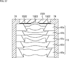
図16に示されるカメラモジュール1Fにおいても、図13に示したカメラモジュール1Dと同様に、入射した光が、絞り板51で絞られた後、積層レンズ構造体11の内部で広がり、積層レンズ構造体11の下方に配置された受光素子12へと入射される。すなわち、積層レンズ構造体11全体について概観すると、光は、絞り板51の開口部52から下側に向かって、末広がりに広がって進行する。 In the camera module 1F shown in FIG. 16, similarly to the camera module 1D shown in FIG. 13, the incident light is focused by the diaphragm plate 51 and then spreads inside the laminated lens structure 11 to form a laminated lens structure. It is incident on the light receiving element 12 arranged below the body 11. That is, when the entire laminated lens structure 11 is reviewed, the light spreads toward the lower side from the opening 52 of the diaphragm plate 51 and travels.

図16のカメラモジュール1Fは、積層レンズ構造体11を構成する各レンズ付き基板41の貫通孔83の断面形状が、下側(受光素子12を配置する側)に向かって開口幅が大きくなる、いわゆる末広がりの形状となっている点が、図13に示したカメラモジュール1Dと異なる。 In the camera module 1F of FIG. 16, the cross-sectional shape of the through hole 83 of each lens-equipped substrate 41 constituting the laminated lens structure 11 increases in opening width toward the lower side (the side on which the light receiving element 12 is arranged). It differs from the camera module 1D shown in FIG. 13 in that it has a so-called divergent shape.

カメラモジュール1Fの積層レンズ構造体11は、入射した光が、絞り板51の開口部52から下側に向かって末広がりに広がって進行する構造であるため、貫通孔83の開口幅が下側向かって大きくなる末広がり形状は、貫通孔83の開口幅が下側に向かって小さくなる下すぼみ形状よりも、例えば、担体基板81が光路の邪魔になりにくい。これにより、レンズ設計の自由度が高いという作用をもたらす。 Since the laminated lens structure 11 of the camera module 1F has a structure in which the incident light spreads downward from the opening 52 of the diaphragm plate 51 toward the lower side, the opening width of the through hole 83 is directed downward. For example, the carrier substrate 81 is less likely to obstruct the optical path in the divergent shape that becomes larger than the downward dent shape in which the opening width of the through hole 83 decreases downward. This has the effect of increasing the degree of freedom in lens design.

また、担持部92を含めたレンズ樹脂部82の基板平面方向の断面積は、貫通孔83の開口幅が下側に向かって小さくなる下すぼみ形状の場合、レンズ樹脂部82の下面においては、レンズ21に入射した光線を透過させるために特定の大きさとなり、かつ、レンズ樹脂部82の下面から上面に向かって、その断面積が大きくなって行く。 Further, when the cross-sectional area of the lens resin portion 82 including the supporting portion 92 in the substrate plane direction is a downward recess shape in which the opening width of the through hole 83 decreases downward, the lower surface of the lens resin portion 82 may have a cross-sectional area. It has a specific size for transmitting light rays incident on the lens 21, and its cross-sectional area increases from the lower surface to the upper surface of the lens resin portion 82.

これに対して、貫通孔83の開口幅が下側向かって大きくなる末広がり形状の場合、レンズ樹脂部82の下面における断面積は、下すぼみ形状の場合と概ね同じとなるが、レンズ樹脂部82の下面から上面に向かって、その断面積が小さくなって行く。 On the other hand, in the case of the divergent shape in which the opening width of the through hole 83 increases downward, the cross-sectional area on the lower surface of the lens resin portion 82 is substantially the same as in the case of the downward recessed shape, but the lens resin portion 82. The cross-sectional area of the lens decreases from the lower surface to the upper surface.

これにより、貫通孔83の開口幅が下側に向かって大きくなる構造は、担持部92を含めたレンズ樹脂部82の大きさを、小さく抑えることができるという作用または効果をもたらす。また、これにより、先に述べたレンズが大きい場合に生じるレンズ形成の難しさを、低減できるという作用または効果をもたらす。 As a result, the structure in which the opening width of the through hole 83 increases downward brings about an action or effect that the size of the lens resin portion 82 including the supporting portion 92 can be suppressed to a small size. Further, this brings about an action or effect that the difficulty of lens formation that occurs when the lens is large as described above can be reduced.

<8.カメラモジュールの第7の実施の形態>
図17は、本技術を適用した積層レンズ構造体を用いたカメラモジュールの第7の実施の形態を示す図である。
<8. Seventh Embodiment of the camera module>
FIG. 17 is a diagram showing a seventh embodiment of a camera module using a laminated lens structure to which the present technology is applied.

図17においても、図13と対応する部分については同一の符号を付してあり、図13に示したカメラモジュール1Dと異なる部分に注目して説明する。 Also in FIG. 17, the parts corresponding to those in FIG. 13 are designated by the same reference numerals, and the parts different from the camera module 1D shown in FIG. 13 will be mainly described.

図17のカメラモジュール1Gは、やはり、積層レンズ構造体11を構成する各レンズ付き基板41のレンズ樹脂部82と貫通孔83の形状が、図13に示したカメラモジュール1Dと異なる。 The camera module 1G of FIG. 17 is also different from the camera module 1D shown in FIG. 13 in the shapes of the lens resin portion 82 and the through hole 83 of each lens-attached substrate 41 constituting the laminated lens structure 11.

カメラモジュール1Gの積層レンズ構造体11は、貫通孔83の形状が、下側(受光素子12を配置する側)に向かって開口幅が小さくなる、いわゆる下すぼみの形状となったレンズ付き基板41と、貫通孔83の形状が、下側に向かって開口幅が大きくなる、いわゆる末広がりの形状となったレンズ付き基板41と、の双方を備える。 The laminated lens structure 11 of the camera module 1G has a substrate 41 with a lens in which the shape of the through hole 83 is a so-called downward recess in which the opening width becomes smaller toward the lower side (the side where the light receiving element 12 is arranged). And the substrate 41 with a lens in which the shape of the through hole 83 has a so-called divergent shape in which the opening width increases toward the lower side.

貫通孔83が、下側に向かって開口幅が小さくなる、いわゆる下すぼみの形状となったレンズ付き基板41は、先に述べたように、貫通孔83の側壁に当たった射入射光85が、上側方向いわゆる入射側方向へと反射され、これにより迷光あるいはノイズ光の発生を抑える、という作用または効果をもたらす。 As described above, the lens-equipped substrate 41 in which the through hole 83 has a so-called downward recessed shape in which the opening width becomes smaller toward the lower side receives the emitted incident light 85 that hits the side wall of the through hole 83. , It is reflected in the upper direction, that is, the incident side direction, which has the effect or effect of suppressing the generation of stray light or noise light.

そこで、図17の積層レンズ構造体11においては、積層レンズ構造体11を構成する複数枚のレンズ付き基板41のうち、特に上側(入射側)の複数枚において、貫通孔83が、下側に向かって開口幅が小さくなる、いわゆる下すぼみの形状となったレンズ付き基板41が用いられている。 Therefore, in the laminated lens structure 11 of FIG. 17, the through hole 83 is on the lower side, particularly on the upper side (incident side) of the plurality of lens-attached substrates 41 constituting the laminated lens structure 11. A substrate 41 with a lens having a so-called downward recess shape in which the opening width becomes smaller toward the end is used.

貫通孔83が、下側に向かって開口幅が大きくなる、いわゆる末広がりの形状となったレンズ付き基板41は、先に述べたように、レンズ付き基板41に備わる担体基板81が光路の邪魔となりにくく、これによって、レンズ設計の自由度が増す、あるいは、レンズ付き基板41に備わる担持部92を含めたレンズ樹脂部82の大きさを小さく抑える、という作用または効果をもたらす。 In the lens-equipped substrate 41 in which the through hole 83 has a so-called divergent shape in which the opening width increases toward the lower side, as described above, the carrier substrate 81 provided in the lens-equipped substrate 41 obstructs the optical path. It is difficult, and this increases the degree of freedom in lens design, or brings about the action or effect of suppressing the size of the lens resin portion 82 including the supporting portion 92 provided on the lens-attached substrate 41 to a small size.

図17の積層レンズ構造体11においては、光は絞りから下側に向かって、末広がりに広がって進行するため、積層レンズ構造体11を構成する複数枚のレンズ付き基板41のうち、下側に配置した何枚かのレンズ付き基板41に備わるレンズ樹脂部82の大きさが大きい。このような大きいレンズ樹脂部82において、末広がりの形状の貫通孔83を用いると、レンズ樹脂部82の大きさを抑制する作用が大きく現れる。 In the laminated lens structure 11 of FIG. 17, since the light spreads toward the lower side from the diaphragm and travels divergently, it is located on the lower side of the plurality of lens-attached substrates 41 constituting the laminated lens structure 11. The size of the lens resin portion 82 provided on some of the arranged substrates 41 with lenses is large. When the through hole 83 having a divergent shape is used in such a large lens resin portion 82, the effect of suppressing the size of the lens resin portion 82 is greatly exhibited.

そこで、図17の積層レンズ構造体11においては、積層レンズ構造体11を構成する複数枚のレンズ付き基板41のうち、特に下側の複数枚において、貫通孔83が、下側に向かって開口幅が大きくなる、いわゆる末広がりの形状となったレンズ付き基板41を用いている。 Therefore, in the laminated lens structure 11 of FIG. 17, the through hole 83 opens toward the lower side, particularly in the lower plurality of the plurality of lens-attached substrates 41 constituting the laminated lens structure 11. A substrate 41 with a lens having a so-called divergent shape having a large width is used.

<9.レンズ付き基板の詳細構成>
次に、レンズ付き基板41の詳細構成について説明する。
<9. Detailed configuration of substrate with lens>
Next, the detailed configuration of the substrate 41 with a lens will be described.

図18は、レンズ付き基板41の詳細構成を示す断面図である。 FIG. 18 is a cross-sectional view showing a detailed configuration of the substrate 41 with a lens.

なお、図18では、5枚のレンズ付き基板41a乃至41eのうちの、最上層のレンズ付き基板41aが図示されているが、その他のレンズ付き基板41も同様に構成されている。 In FIG. 18, of the five lens-attached substrates 41a to 41e, the uppermost lens-attached substrate 41a is shown, but the other lens-attached substrates 41 are similarly configured.

レンズ付き基板41の構成としては、図18のA乃至Cのいずれかの構成をとることができる。 As the configuration of the substrate 41 with a lens, any of the configurations A to C in FIG. 18 can be adopted.

図18のAに示されるレンズ付き基板41には、担体基板81に設けられた貫通孔83に対して、上面からみて貫通孔83を塞ぐようにレンズ樹脂部82が形成されている。レンズ樹脂部82は、図14を参照して説明したように、中央部のレンズ部91(不図示)と、その周辺部の担持部92(不図示)で構成される。 In the substrate 41 with a lens shown in FIG. 18A, a lens resin portion 82 is formed so as to close the through hole 83 when viewed from the upper surface with respect to the through hole 83 provided in the carrier substrate 81. As described with reference to FIG. 14, the lens resin portion 82 includes a lens portion 91 (not shown) in the central portion and a supporting portion 92 (not shown) in the peripheral portion thereof.

レンズ付き基板41の貫通孔83となる側壁には、光反射を起因とするゴーストやフレアを防止するために光吸収性もしくは遮光性を有する膜121が成膜されている。これらの膜121を便宜的に遮光膜121と呼ぶ。 A film 121 having light absorption or light shielding properties is formed on the side wall of the lens-equipped substrate 41, which is a through hole 83, in order to prevent ghosts and flares caused by light reflection. These films 121 are conveniently referred to as light-shielding films 121.

担体基板81とレンズ樹脂部82の上側表面には、酸化物もしくは窒化物あるいはその他の絶縁物を含む上側表面層122が形成されており 、担体基板81とレンズ樹脂部82の下側表面には、酸化物もしくは窒化物あるいはその他の絶縁物を含む下側表面層123が形成されている。 An upper surface layer 122 containing an oxide, a nitride, or other insulating material is formed on the upper surface of the carrier substrate 81 and the lens resin portion 82, and the lower surface of the carrier substrate 81 and the lens resin portion 82 is formed. A lower surface layer 123 containing oxides or nitrides or other insulators is formed.

上側表面層122は、一例として、低屈折膜と高屈折膜を交互に複数層積層した反射防止膜を構成している。反射防止膜は、例えば、低屈折膜と高屈折膜を交互に合計4層積層して構成することができる。低屈折膜は、例えば、SiOx(1≦x≦2)、SiOC、SiOFなどの酸化膜、高屈折膜は、例えば、TiO、TaO、Nb2O5などの金属酸化膜で構成される。 As an example, the upper surface layer 122 constitutes an antireflection film in which a plurality of layers of low-refractive film and high-refractive film are alternately laminated. The antireflection film can be formed by, for example, alternately laminating a total of four layers of low-refractive film and high-refractive film. The low refraction film is composed of, for example, an oxide film such as SiOx (1 ≦ x ≦ 2), SiOC, SiOF, and the high refraction film is composed of, for example, a metal oxide film such as TiO, TaO, Nb2O5.

なお、上側表面層122の構成は、例えば、光学シミュレーションを用いて所望の反射防止性能が得られるように設計されていればよく、低屈折膜及び高屈折膜の材料、膜厚、積層数などは特に限定されない。本実施の形態では、上側表面層122の最表面は、低屈折膜となっており、その膜厚は、例えば20乃至1000nm、密度は、例えば2.2乃至2.5g/cm3、平坦度が、例えば1nm以下程度の二乗平均粗さRq(RMS)となっている。また、詳細は後述するが、この上側表面層122は、他のレンズ付き基板41と接合される際の接合膜にもなっている。 The structure of the upper surface layer 122 may be designed so as to obtain desired antireflection performance by using, for example, optical simulation, and the material, film thickness, number of layers, etc. of the low refraction film and the high refraction film may be obtained. Is not particularly limited. In the present embodiment, the outermost surface of the upper surface layer 122 is a low-refractive film, the thickness thereof is, for example, 20 to 1000 nm, the density is, for example, 2.2 to 2.5 g / cm3, and the flatness is high. For example, the root mean square roughness Rq (RMS) is about 1 nm or less. Further, as will be described in detail later, the upper surface layer 122 also serves as a bonding film when bonded to another substrate with a lens 41.

上側表面層122は、一例として、低屈折膜と高屈折膜を交互に複数層積層した反射防止膜であって良く、そのなかでも無機物の反射防止膜であって良い。上側表面層122は、別の例として、酸化物もしくは窒化物あるいはその他の絶縁物を含む単層膜であっても良く、そのなかでも無機物の膜であっても良い。 As an example, the upper surface layer 122 may be an antireflection film in which a plurality of layers of a low refraction film and a high refraction film are alternately laminated, and among them, an inorganic antireflection film may be used. As another example, the upper surface layer 122 may be a single-layer film containing an oxide, a nitride, or other insulating material, and may be an inorganic film.

下側表面層123も、一例として、低屈折膜と高屈折膜を交互に複数層積層した反射防止膜であって良く、そのなかでも無機物の反射防止膜であって良い。下側表面層123は、別の例として、酸化物もしくは窒化物あるいはその他の絶縁物を含む単層膜であっても良く、そのなかでも無機物の膜であっても良い。 As an example, the lower surface layer 123 may be an antireflection film in which a plurality of layers of a low refraction film and a high refraction film are alternately laminated, and among them, an inorganic antireflection film may be used. As another example, the lower surface layer 123 may be a single-layer film containing an oxide, a nitride, or other insulating material, and may be an inorganic film.

図18のB及びCのレンズ付き基板41については、図18のAに示したレンズ付き基板41と異なる部分についてのみ説明する。 The lens-equipped substrates 41 of B and C in FIG. 18 will be described only in a portion different from the lens-attached substrate 41 shown in A of FIG.

図18のBに示されるレンズ付き基板41においては、担体基板81とレンズ樹脂部82の下側表面に形成されている膜が、図18のAに示したレンズ付き基板41と異なる。 In the lens-attached substrate 41 shown in FIG. 18B, the film formed on the lower surface of the carrier substrate 81 and the lens resin portion 82 is different from the lens-attached substrate 41 shown in FIG. 18A.

図18のBのレンズ付き基板41では、担体基板81の下側表面には、酸化物もしくは窒化物あるいはその他の絶縁物を含む下側表面層124が形成されている一方、レンズ樹脂部82の下側表面には、下側表面層124が形成されていない。下側表面層124は、上側表面層122と同一材料でもよいし、異なる材料でもよい。 In the lens-attached substrate 41 of FIG. 18B, a lower surface layer 124 containing an oxide, a nitride, or other insulating material is formed on the lower surface of the carrier substrate 81, while the lens resin portion 82 of the lens resin portion 82. The lower surface layer 124 is not formed on the lower surface. The lower surface layer 124 may be made of the same material as the upper surface layer 122, or may be made of a different material.

このような構造は、例えば、レンズ樹脂部82を形成する前に、担体基板81の下側表面に下側表面層124を形成しておき、その後、レンズ樹脂部82を形成する製法により、形成し得る。あるいは、レンズ樹脂部82を形成した後に、レンズ樹脂部82にマスクを形成し、担体基板81上にはマスクを形成しない状態で、下側表面層124を構成する膜を、例えばPVDにより、担体基板81の下側表面に堆積させることで、形成し得る。 Such a structure is formed, for example, by a manufacturing method in which a lower surface layer 124 is formed on the lower surface of the carrier substrate 81 before the lens resin portion 82 is formed, and then the lens resin portion 82 is formed. Can be done. Alternatively, after the lens resin portion 82 is formed, a mask is formed on the lens resin portion 82, and the film constituting the lower surface layer 124 is formed on the carrier substrate 81 without forming the mask, for example, by using PVD as a carrier. It can be formed by depositing it on the lower surface of the substrate 81.

図18のCのレンズ付き基板41においては、担体基板81の上側表面に、酸化物もしくは窒化物あるいはその他の絶縁物を含む上側表面層125が形成されている一方、レンズ樹脂部82の上側表面には、上側表面層125が形成されていない。 In the lens-attached substrate 41 of FIG. 18C, an upper surface layer 125 containing an oxide, a nitride, or other insulating material is formed on the upper surface of the carrier substrate 81, while the upper surface of the lens resin portion 82 is formed. The upper surface layer 125 is not formed on the surface.

同様に、レンズ付き基板41の下側表面においても、担体基板81の下側表面に、酸化物もしくは窒化物あるいはその他の絶縁物を含む下側表面層124が形成されている一方、レンズ樹脂部82の下側表面には、下側表面層124が形成されていない。 Similarly, on the lower surface of the lens-attached substrate 41, the lower surface layer 124 containing an oxide, a nitride, or other insulating material is formed on the lower surface of the carrier substrate 81, while the lens resin portion. The lower surface layer 124 is not formed on the lower surface of 82.

このような構造は、例えば、レンズ樹脂部82が形成される前に、担体基板81に上側表面層125と下側表面層124を形成しておき、その後、レンズ樹脂部82を形成する製法により、形成し得る。あるいは、レンズ樹脂部82を形成した後に、レンズ樹脂部82にマスクを形成し、担体基板81上にはマスクを形成しない状態で、上側表面層125および下側表面層124を構成する膜を、例えばPVDにより、担体基板81の表面に堆積させることで、形成し得る。下側表面層124と上側表面層125は、同一材料でもよいし、異なる材料でもよい。 Such a structure is obtained, for example, by a manufacturing method in which an upper surface layer 125 and a lower surface layer 124 are formed on the carrier substrate 81 before the lens resin portion 82 is formed, and then the lens resin portion 82 is formed. , Can be formed. Alternatively, after the lens resin portion 82 is formed, a mask is formed on the lens resin portion 82, and the films forming the upper surface layer 125 and the lower surface layer 124 are formed on the carrier substrate 81 without forming the mask. It can be formed by depositing it on the surface of the carrier substrate 81, for example, by PVD. The lower surface layer 124 and the upper surface layer 125 may be made of the same material or different materials.

レンズ付き基板41は、以上のように構成することができる。 The substrate 41 with a lens can be configured as described above.

<10.レンズ付き基板の製造方法>
次に、図19乃至図29を参照して、レンズ付き基板41の製造方法を説明する。
<10. Manufacturing method of substrate with lens >
Next, a method of manufacturing the lens-attached substrate 41 will be described with reference to FIGS. 19 to 29.

初めに、複数の貫通孔83が形成された基板状態の担体基板81Wが用意される。担体基板81Wは、例えば、通常の半導体装置に用いる、シリコンの基板を用いることができる。担体基板81Wの形状は、例えば図19のAに示されるような円形で、その直径は、例えば200mmや300mmなどとされる。担体基板81Wは、シリコンの基板ではなく、例えば、ガラスの基板、樹脂の基板、あるいは金属の基板であっても良い。 First, a carrier substrate 81W in a substrate state in which a plurality of through holes 83 are formed is prepared. As the carrier substrate 81W, for example, a silicon substrate used in a normal semiconductor device can be used. The shape of the carrier substrate 81W is, for example, a circle as shown in FIG. 19A, and the diameter thereof is, for example, 200 mm or 300 mm. The carrier substrate 81W may be, for example, a glass substrate, a resin substrate, or a metal substrate instead of the silicon substrate.

また、貫通孔83の平面形状は、本実施の形態では、図19のAに示されるように円形であるとするが、図19のBに示されるように、貫通孔83の平面形状は、例えば四角形などの多角形であっても良い。 Further, in the present embodiment, the planar shape of the through hole 83 is circular as shown in A of FIG. 19, but as shown in B of FIG. 19, the planar shape of the through hole 83 is For example, it may be a polygon such as a quadrangle.

貫通孔83の開口幅は、例えば、100μm程度から20mm程度まで採り得る。この場合、担体基板81Wには、例えば100個程度から500万個程度まで配置し得る。 The opening width of the through hole 83 can be, for example, from about 100 μm to about 20 mm. In this case, for example, about 100 to about 5 million can be arranged on the carrier substrate 81W.

本明細書においては、レンズ付き基板41の平面方向における貫通孔83の大きさを、開口幅と呼ぶ。開口幅は、特に断り書きがが無い限り、貫通孔83の平面形状が四角形である場合は一辺の長さ、貫通孔83の平面形状が円形である場合は直径を意味する。 In the present specification, the size of the through hole 83 in the plane direction of the lens-equipped substrate 41 is referred to as an opening width. Unless otherwise specified, the opening width means the length of one side when the plane shape of the through hole 83 is quadrangular, and the diameter when the plane shape of the through hole 83 is circular.

貫通孔83は、図20に示されるように、担体基板81Wの第1の表面における第1の開口幅131よりも、第1の表面と対向する第2の表面における第2の開口幅132の方が、小さくなっている。 As shown in FIG. 20, the through hole 83 has a second opening width 132 on the second surface facing the first surface rather than the first opening width 131 on the first surface of the carrier substrate 81W. Is smaller.

第1の開口幅131よりも第2の開口幅132の方が小さい貫通孔83の3次元形状の例として、貫通孔83は、図20のAに示される円錐台の形状であって良いし、多角形の角錐台の形状であっても良い。貫通孔83の側壁の断面形状は、図20のAに示されるような直線であって良いし、図20のBに示されるような曲線であってもよい。あるいはまた、図20のCに示されるように、段差があっても良い。 As an example of the three-dimensional shape of the through hole 83 in which the second opening width 132 is smaller than the first opening width 131, the through hole 83 may have the shape of the truncated cone shown in FIG. 20A. , It may be in the shape of a polygonal truncated cone. The cross-sectional shape of the side wall of the through hole 83 may be a straight line as shown in A of FIG. 20 or a curved line as shown in B of FIG. Alternatively, as shown in FIG. 20C, there may be a step.

第1の開口幅131よりも第2の開口幅132の方が小さい形状である貫通孔83は、貫通孔83内に樹脂を供給し、この樹脂を、第1と第2の表面のそれぞれから対向する方向へ型部材で押すことでレンズ樹脂部82を形成する際に、レンズ樹脂部82となる樹脂が、対向する2つの型部材からの力を受けて、貫通孔83の側壁に押し付けられる。これにより、レンズ樹脂部82となる樹脂と担体基板との密着強度が高くなるという作用をもたらし得る。 The through hole 83, which has a shape in which the second opening width 132 is smaller than the first opening width 131, supplies a resin into the through hole 83, and this resin is supplied from each of the first and second surfaces. When the lens resin portion 82 is formed by pushing the lens resin portion 82 in the opposite direction with the mold member, the resin to be the lens resin portion 82 is pressed against the side wall of the through hole 83 by receiving the force from the two opposing mold members. .. This can bring about the effect of increasing the adhesion strength between the resin to be the lens resin portion 82 and the carrier substrate.

なお、貫通孔83の他の実施の形態として、第1の開口幅131と第2の開口幅132が等しい形状、すなわち貫通孔83の側壁の断面形状が垂直となる形状であっても良い。 As another embodiment of the through hole 83, the first opening width 131 and the second opening width 132 may have the same shape, that is, the cross-sectional shape of the side wall of the through hole 83 may be vertical.

<ウェットエッチングを用いた貫通孔の形成方法>
担体基板81Wの貫通孔83は、担体基板81Wをウェットエッチングにより、エッチングすることによって形成することができる。具体的には、担体基板81Wをエッチングする前に、担体基板81Wの非開口領域がエッチングされることを防ぐためのエッチングマスクが、担体基板81Wの表面に形成される。エッチングマスクの材料には、例えばシリコン酸化膜あるいはシリコン窒化膜などの絶縁膜が用いられる。エッチングマスクは、エッチングマスク材料の層を担体基板81Wの表面に形成し、この層に貫通孔83の平面形状となるパターンを開口することで、形成される。エッチングマスクが形成された後、担体基板81Wをエッチングすることにより、担体基板81Wに貫通孔83が形成される。
<Method of forming through holes using wet etching>
The through hole 83 of the carrier substrate 81W can be formed by etching the carrier substrate 81W by wet etching. Specifically, before etching the carrier substrate 81W, an etching mask for preventing the non-open area of the carrier substrate 81W from being etched is formed on the surface of the carrier substrate 81W. As the material of the etching mask, for example, an insulating film such as a silicon oxide film or a silicon nitride film is used. The etching mask is formed by forming a layer of the etching mask material on the surface of the carrier substrate 81W and opening a planar pattern of the through holes 83 in this layer. After the etching mask is formed, the carrier substrate 81W is etched to form a through hole 83 in the carrier substrate 81W.

担体基板81Wとして、例えば、基板表面方位が(100)の単結晶シリコンを使用する場合、貫通孔83を形成するためには、KOHなどのアルカリ性の溶液を用いた結晶異方性ウェットエッチングを採用することができる。 When, for example, single crystal silicon having a substrate surface orientation of (100) is used as the carrier substrate 81W, crystal anisotropic wet etching using an alkaline solution such as KOH is adopted to form the through holes 83. can do.

基板表面方位が(100)の単結晶シリコンである担体基板81Wに、KOHなどのアルカリ性の溶液を用いた結晶異方性ウェットエッチングを行うと、開口側壁に(111)面が現れるようにエッチングが進行する。その結果、エッチングマスクの開口部の平面形状が円形もしくは四角形のどちらであっても、平面形状が四角形であって、貫通孔83の開口幅は第1の開口幅131よりも第2の開口幅132の方が小さく、貫通孔83の3次元形状が角錐台もしくはこれに類似の形状となる貫通孔83が得られる。角錐台となる貫通孔83の側壁の角度は、基板平面に対して、約55°の角度となる。 When crystal anisotropic wet etching using an alkaline solution such as KOH is performed on a carrier substrate 81W which is a single crystal silicon having a substrate surface orientation of (100), the etching is performed so that the (111) plane appears on the opening side wall. proceed. As a result, regardless of whether the planar shape of the opening of the etching mask is circular or quadrangular, the planar shape is quadrangular, and the opening width of the through hole 83 is a second opening width rather than the first opening width 131. 132 is smaller, and a through hole 83 having a three-dimensional shape of the through hole 83 having a pyramid base or a shape similar thereto can be obtained. The angle of the side wall of the through hole 83, which is the pyramid base, is about 55 ° with respect to the substrate plane.

貫通孔形成のためのエッチングは、別の実施の例として、国際公開第2011/010739号などに開示された、結晶方位の制約を受けずに任意の形状にシリコンをエッチング可能な薬液を用いたウェットエッチングによって行っても良い。この薬液としては、例えば、TMAH(水酸化テトラメチルアンモニウム)水溶液に、界面活性剤であるポリオキシエチレンアルキルフェニルエーテル、ポリオキシアルキレンアルキルエーテル、ポリエチレングリコールの少なくとも1つを加えた薬液、もしくは、KOH水溶液にイソプロピルアルコールを加えた薬液、などを採用することができる。 For the etching for forming the through hole, as another example of implementation, a chemical solution disclosed in International Publication No. 2011/010739, etc., which can etch silicon into an arbitrary shape without being restricted by the crystal orientation, was used. It may be performed by wet etching. The chemical solution includes, for example, a chemical solution obtained by adding at least one of a surfactant, polyoxyethylene alkylphenyl ether, polyoxyalkylene alkyl ether, or polyethylene glycol, to an aqueous solution of TMAH (tetramethylammonium hydroxide), or KOH. A chemical solution obtained by adding isopropyl alcohol to an aqueous solution can be adopted.

基板表面方位が(100)の単結晶シリコンである担体基板81Wに、上述したいずれかの薬液を用いて貫通孔83形成のためのエッチングを行うと、エッチングマスクの開口部の平面形状が円形である場合は、平面形状が円形であって、第1の開口幅131よりも第2の開口幅132の方が小さく、3次元形状が円錐台もしくはこれに類似の形状、となる貫通孔83が得られる。 When the carrier substrate 81W, which is a single crystal silicon having a substrate surface orientation of (100), is etched for forming the through hole 83 using any of the above-mentioned chemical solutions, the planar shape of the opening of the etching mask becomes circular. In some cases, the through hole 83 has a circular planar shape, the second opening width 132 is smaller than the first opening width 131, and the three-dimensional shape is a truncated cone or a similar shape. can get.

エッチングマスクの開口部の平面形状が四角形である場合には、平面形状が四角形であって、開口幅は第1の開口幅131よりも第2の開口幅132の方が小さく、3次元形状が角錐台もしくはこれに類似の形状、となる貫通孔83が得られる。上記円錐台もしくは角錐台となる貫通孔83の側壁の角度は、基板平面に対して、約45°の角度となる。 When the planar shape of the opening of the etching mask is quadrangular, the planar shape is quadrangular, and the opening width is smaller in the second opening width 132 than in the first opening width 131, and the three-dimensional shape is large. A through hole 83 having a shape similar to that of a pyramidal table can be obtained. The angle of the side wall of the through hole 83, which is the truncated cone or the truncated cone, is about 45 ° with respect to the substrate plane.

<ドライエッチングを用いた貫通孔の形成方法>
また、貫通孔83形成のエッチングには、上述したウェットエッチングではなく、ドライエッチングを用いることも可能である。
<Method of forming through holes using dry etching>
Further, it is also possible to use dry etching instead of the wet etching described above for the etching for forming the through hole 83.

図21を参照して、ドライエッチングを用いた貫通孔83の形成方法について説明する。 A method of forming the through hole 83 using dry etching will be described with reference to FIG.

図21のAに示されるように、担体基板81Wの一方の表面に、エッチングマスク141が形成される。エッチングマスク141は、貫通孔83を形成する部分が開口されたマスクパターンとなっている。 As shown in FIG. 21A, an etching mask 141 is formed on one surface of the carrier substrate 81W. The etching mask 141 has a mask pattern in which a portion forming the through hole 83 is opened.

次に、図21のBに示されるように、エッチングマスク141の側壁を保護するための保護膜142が形成された後、図21のCに示されるように、ドライエッチングにより担体基板81Wが所定の深さでエッチングされる。ドライエッチング工程により、担体基板81W表面とエッチングマスク141表面の保護膜142は除去されるが、エッチングマスク141側面の保護膜142は残存し、エッチングマスク141の側壁は保護される。エッチング後、図21のDに示されるように、側壁の保護膜142が除去され、エッチングマスク141が、開口パターンのパターンサイズを大きくする方向に後退される。 Next, as shown in FIG. 21B, after the protective film 142 for protecting the side wall of the etching mask 141 is formed, as shown in FIG. 21C, the carrier substrate 81W is predetermined by dry etching. Etched to the depth of. By the dry etching step, the protective film 142 on the surface of the carrier substrate 81W and the surface of the etching mask 141 is removed, but the protective film 142 on the side surface of the etching mask 141 remains, and the side wall of the etching mask 141 is protected. After etching, as shown in D of FIG. 21, the protective film 142 on the side wall is removed, and the etching mask 141 is retracted in the direction of increasing the pattern size of the opening pattern.

そして、再び、図21のB乃至Dの保護膜形成工程、ドライエッチング工程、エッチングマスク後退工程が、複数回繰り返し行われる。これにより、図21のEに示されるように、担体基板81Wは、周期性のある段差を持つ階段形状(凹凸形状)となるようにエッチングされる。 Then, the protective film forming step, the dry etching step, and the etching mask retreating step of FIGS. 21B are repeated a plurality of times again. As a result, as shown in E of FIG. 21, the carrier substrate 81W is etched so as to have a stepped shape (concave and convex shape) having a periodic step.

最後に、エッチングマスク141が除去されると、図21のFに示されるように、階段形状の側壁をもつ貫通孔83が、担体基板81Wに形成される。貫通孔83の階段形状の平面方向の幅(1段の幅)は、例えば、400nm乃至1μm程度とされる。 Finally, when the etching mask 141 is removed, a through hole 83 having a stepped side wall is formed in the carrier substrate 81W, as shown in F of FIG. The width of the stepped hole 83 in the plane direction (width of one step) is, for example, about 400 nm to 1 μm.

以上のようにドライエッチングを用いて貫通孔83を形成する場合には、保護膜形成工程、ドライエッチング工程、エッチングマスク後退工程が繰り返し実行される。 When the through hole 83 is formed by dry etching as described above, the protective film forming step, the dry etching step, and the etching mask retreating step are repeatedly executed.

貫通孔83の側壁が周期性のある階段形状(凹凸形状)であることにより、入射光の反射を抑制することができる。また、仮に、貫通孔83の側壁がランダムな大きさの凹凸形状である場合には、貫通孔83内に形成されるレンズと側壁との間の密着層にボイド(空隙)が発生し、そのボイドが原因でレンズとの密着性が低下する場合がある。しかしながら、上述した形成方法によれば、貫通孔83の側壁は周期性のある凹凸形状となるので、密着性が向上し、レンズ位置ずれによる光学特性の変化を抑制することができる。 Since the side wall of the through hole 83 has a periodic staircase shape (concave and convex shape), reflection of incident light can be suppressed. Further, if the side wall of the through hole 83 has a concave-convex shape of a random size, a void (void) is generated in the close contact layer between the lens and the side wall formed in the through hole 83. Adhesion to the lens may decrease due to voids. However, according to the above-mentioned forming method, since the side wall of the through hole 83 has a periodic concave-convex shape, the adhesion is improved and the change in the optical characteristics due to the lens misalignment can be suppressed.

各工程で使用される材料の一例としては、例えば、担体基板81Wは単結晶シリコン、エッチングマスク141はフォトレジスト、保護膜142は、C4F8やCHF3などのガスプラズマを用いて形成するフロカーボンポリマー、エッチング処理は、SF6/O2、C4F8/SF6などFを含むガスを用いたプラズマエッチング、マスク後退工程は、O2ガス、CF4/O2などO2を含むプラズマエッチングとすることができる。 As an example of the material used in each step, for example, the carrier substrate 81W is a single crystal silicon, the etching mask 141 is a photoresist, and the protective film 142 is a fluorocarbon polymer formed by using gas plasma such as C4F8 or CHF3. The etching process can be plasma etching using gas containing F such as SF6 / O2 and C4F8 / SF6, and the mask retreat step can be plasma etching using O2 gas and gas containing O2 such as CF4 / O2.

あるいはまた、担体基板81Wは単結晶シリコン、エッチングマスク141はSiO2、エッチングは、Cl2を含むプラズマ、保護膜142は、O2プラズマを用いてエッチング対象材を酸化させた酸化膜、エッチング処理は、Cl2を含むガスを用いたプラズマエッチングマスク後退工程は、CF4/O2などFを含むガスを用いたプラズマエッチングとすることができる。 Alternatively, the carrier substrate 81W is monocrystalline silicon, the etching mask 141 is SiO2, the etching is plasma containing Cl2, the protective film 142 is an oxide film obtained by oxidizing the material to be etched using O2 plasma, and the etching process is Cl2. The plasma etching mask retreat step using a gas containing F can be plasma etching using a gas containing F such as CF4 / O2.

以上のように、ウェットエッチング、または、ドライエッチングにより、担体基板81Wに、複数の貫通孔83を同時形成することができるが、担体基板81Wには、図22のAに示されるように、貫通孔83を形成していない領域に貫通溝151を形成しても良い。 As described above, a plurality of through holes 83 can be simultaneously formed in the carrier substrate 81W by wet etching or dry etching, but the carrier substrate 81W is penetrated as shown in FIG. 22A. A through groove 151 may be formed in a region where the hole 83 is not formed.

図22のAは、貫通孔83に加えて貫通溝151を形成した担体基板81Wの平面図である。 FIG. 22A is a plan view of the carrier substrate 81W in which the through groove 151 is formed in addition to the through hole 83.

貫通溝151は、例えば、図22のAに示されるように、行列状に配置された複数個の貫通孔83を避けて、行方向と列方向のそれぞれの貫通孔83の間の一部にだけ配置される。 The through groove 151 is formed in a part between the through holes 83 in the row direction and the through hole 83 in the column direction, avoiding a plurality of through holes 83 arranged in a matrix, for example, as shown in A of FIG. Is placed only.

また、担体基板81Wの貫通溝151は、積層レンズ構造体11を構成する各レンズ付き基板41どうしで、同一の位置に配置することができる。この場合には、積層レンズ構造体11として複数枚の担体基板81Wが積層された状態では、図22のBの断面図のように、複数枚の担体基板81Wの貫通溝151が、複数枚の担体基板81Wの間で貫通した構造となる。 Further, the through groove 151 of the carrier substrate 81W can be arranged at the same position between the substrates 41 with lenses constituting the laminated lens structure 11. In this case, in a state where a plurality of carrier substrates 81W are laminated as the laminated lens structure 11, a plurality of through grooves 151 of the plurality of carrier substrates 81W are formed as shown in the cross-sectional view of FIG. 22B. The structure is such that it penetrates between the carrier substrates 81W.

レンズ付き基板41の一部としての担体基板81Wの貫通溝151は、例えば、レンズ付き基板41を変形させる応力がレンズ付き基板41の外部から働く場合に、応力によるレンズ付き基板41の変形を緩和する作用または効果をもたらし得る。 The through groove 151 of the carrier substrate 81W as a part of the lens-attached substrate 41 alleviates the deformation of the lens-attached substrate 41 due to the stress when the stress for deforming the lens-attached substrate 41 acts from the outside of the lens-attached substrate 41, for example. Can bring about an action or effect.

あるいは、貫通溝151は、例えば、レンズ付き基板41を変形させる応力がレンズ付き基板41の内部から発生する場合に、応力によるレンズ付き基板41の変形を緩和する作用または効果をもたらし得る。 Alternatively, the through groove 151 may bring about an action or effect of alleviating the deformation of the lens-attached substrate 41 due to the stress when the stress for deforming the lens-attached substrate 41 is generated from the inside of the lens-attached substrate 41, for example.

<レンズ付き基板の製造方法>
次に、図23を参照して、基板状態のレンズ付き基板41Wの製造方法について説明する。
<Manufacturing method of substrate with lens>
Next, with reference to FIG. 23, a method of manufacturing the substrate 41W with a lens in the substrate state will be described.

初めに、図23のAに示されるように、貫通孔83が複数形成された担体基板81Wが用意される。貫通孔83の側壁には遮光膜121が成膜されている。図23では、紙面の制約上、2個の貫通孔83のみが示されているが、実際には、図19で示したように、担体基板81Wの平面方向に、多数の貫通孔83が形成されている。また、担体基板81Wの外周に近い領域には、位置合わせのためのアライメントマーク(不図示)が形成されている。 First, as shown in FIG. 23A, a carrier substrate 81W on which a plurality of through holes 83 are formed is prepared. A light-shielding film 121 is formed on the side wall of the through hole 83. In FIG. 23, only two through holes 83 are shown due to space limitations, but in reality, as shown in FIG. 19, a large number of through holes 83 are formed in the plane direction of the carrier substrate 81W. Has been done. Further, an alignment mark (not shown) for alignment is formed in a region near the outer circumference of the carrier substrate 81W.

担体基板81W上側の表側平坦部171と、下側の裏側平坦部172は、後の工程で行われるプラズマ接合が可能な程度に平坦に形成された平坦面となっている。担体基板81Wの厚みは、最終的にレンズ付き基板41として個片化され、他のレンズ付き基板41と重ねられた際に、レンズ間距離を決定するスペーサとしての役割も担っている。 The front flat portion 171 on the upper side of the carrier substrate 81W and the back flat portion 172 on the lower side are flat surfaces formed flat enough to allow plasma bonding to be performed in a later step. The thickness of the carrier substrate 81W is finally individualized as a substrate with a lens 41, and when it is overlapped with another substrate with a lens 41, it also plays a role as a spacer for determining the distance between lenses.

担体基板81Wには、熱膨張係数が10ppm/℃以下の低熱膨張係数の基材を用いるのが好ましい。 For the carrier substrate 81W, it is preferable to use a substrate having a low coefficient of thermal expansion of 10 ppm / ° C. or less.

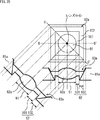
次に、図23のBに示されるように、凹形状の光学転写面182が一定の間隔で複数配置された下型181の上に、担体基板81Wが配置される。より詳しくは、凹形状の光学転写面182が担体基板81Wの貫通孔83の内側に位置するように、担体基板81Wの裏側平坦部172と下型181の平坦面183とが重ね合わされる。下型181の光学転写面182は、担体基板81Wの貫通孔83と1対1に対応するように形成されており、対応する光学転写面182と貫通孔83の中心が光軸方向で一致するように、担体基板81Wと下型181の平面方向の位置が調整される。下型181は、硬質の型部材で形成されており、例えば、金属やシリコン、石英、ガラスで構成される。 Next, as shown in B of FIG. 23, the carrier substrate 81W is arranged on the lower mold 181 in which a plurality of concave optical transfer surfaces 182 are arranged at regular intervals. More specifically, the flat surface 172 on the back side of the carrier substrate 81W and the flat surface 183 of the lower mold 181 are overlapped so that the concave optical transfer surface 182 is located inside the through hole 83 of the carrier substrate 81W. The optical transfer surface 182 of the lower mold 181 is formed so as to correspond one-to-one with the through hole 83 of the carrier substrate 81W, and the centers of the corresponding optical transfer surface 182 and the through hole 83 coincide with each other in the optical axis direction. As described above, the positions of the carrier substrate 81W and the lower mold 181 in the plane direction are adjusted. The lower mold 181 is made of a hard mold member, and is made of, for example, metal, silicon, quartz, or glass.

次に、図23のCに示されるように、重ね合わされた下型181と担体基板81Wの貫通孔83の内側に、エネルギー硬化性樹脂191が充填(滴下)される。レンズ樹脂部82は、このエネルギー硬化性樹脂191を用いて形成される。そのため、エネルギー硬化性樹脂191は、気泡を含まないようにあらかじめ脱泡処理されていることが好ましい。脱泡処理としては、真空脱泡処理、または、遠心力による脱泡処理であることが好ましい。また、真空脱泡処理は充填後に行うことが好ましい。脱泡処理を行うことにより、気泡を抱き込むことなく、レンズ樹脂部82の成形が可能となる。 Next, as shown in C of FIG. 23, the energy curable resin 191 is filled (dropped) inside the through hole 83 of the stacked lower mold 181 and the carrier substrate 81W. The lens resin portion 82 is formed by using this energy curable resin 191. Therefore, the energy curable resin 191 is preferably defoamed in advance so as not to contain air bubbles. The defoaming treatment is preferably a vacuum defoaming treatment or a defoaming treatment by centrifugal force. Further, it is preferable that the vacuum defoaming treatment is performed after filling. By performing the defoaming treatment, the lens resin portion 82 can be molded without embracing air bubbles.

次に、図23のDに示されるように、重ね合わされた下型181と担体基板81Wの上に、上型201が配置される。上型201には、凹形状の光学転写面202が一定の間隔で複数配置されており、下型181を配置したときと同様に、貫通孔83の中心と光学転写面202の中心が光軸方向で一致するように、精度良く位置決めされた上で、上型201が配置される。 Next, as shown in D of FIG. 23, the upper die 201 is arranged on the stacked lower die 181 and the carrier substrate 81W. A plurality of concave optical transfer surfaces 202 are arranged at regular intervals in the upper mold 201, and the center of the through hole 83 and the center of the optical transfer surface 202 are optical axes as in the case where the lower mold 181 is arranged. The upper die 201 is arranged after being accurately positioned so as to match in the direction.

紙面上の縦方向となる高さ方向については、上型201と下型181との間隔を制御する制御装置により、上型201と下型181との間隔が予め定めた距離となるように、上型201の位置が固定される。このとき、上型201の光学転写面202と下型181の光学転写面182とで挟まれる空間は、光学設計によって計算されたレンズ樹脂部82(レンズ21)の厚みと等しくなる。 Regarding the height direction, which is the vertical direction on the paper surface, the control device that controls the distance between the upper mold 201 and the lower mold 181 is used so that the distance between the upper mold 201 and the lower mold 181 is a predetermined distance. The position of the upper die 201 is fixed. At this time, the space sandwiched between the optical transfer surface 202 of the upper mold 201 and the optical transfer surface 182 of the lower mold 181 is equal to the thickness of the lens resin portion 82 (lens 21) calculated by the optical design.

あるいはまた、図23のEに示されるように、下型181を配置したときと同様に、上型201の平坦面203と、担体基板81Wの表側平坦部171とを、重ね合わせても良い。この場合、上型201と下型181との距離は、担体基板81Wの厚みと同値となり、平面方向及び高さ方向の高精度な位置合わせが可能となる。 Alternatively, as shown in E of FIG. 23, the flat surface 203 of the upper die 201 and the front flat portion 171 of the carrier substrate 81W may be overlapped in the same manner as when the lower die 181 is arranged. In this case, the distance between the upper die 201 and the lower die 181 is the same as the thickness of the carrier substrate 81W, and highly accurate positioning in the plane direction and the height direction becomes possible.

上型201と下型181との間隔が予め設定した距離となるように制御したとき、上述した図23のCの工程において、担体基板81Wの貫通孔83の内側に滴下されたエネルギー硬化性樹脂191の充填量は、担体基板81Wの貫通孔83と、その上下の上型201及び下型181とで囲まれる空間から溢れないようにコントロールされた量となっている。これにより、エネルギー硬化性樹脂191の材料を無駄にすることなく、製造コストを削減することができる。 When the distance between the upper mold 201 and the lower mold 181 is controlled to be a preset distance, the energy-curable resin dropped inside the through hole 83 of the carrier substrate 81W in the step C of FIG. 23 described above. The filling amount of 191 is a controlled amount so as not to overflow from the space surrounded by the through hole 83 of the carrier substrate 81W and the upper die 201 and the lower die 181 above and below the through hole 83. As a result, the manufacturing cost can be reduced without wasting the material of the energy curable resin 191.

続いて、図23のEに示される状態において、エネルギー硬化性樹脂191の硬化処理が行われる。エネルギー硬化性樹脂191は、例えば、熱またはUV光をエネルギーとして与え、所定の時間放置することで、硬化する。硬化中には、上型201を下方向に押し込んだり、アライメントをすることにより、エネルギー硬化性樹脂191の収縮による変形を最小限に抑制することができる。 Subsequently, the energy curable resin 191 is cured in the state shown in E of FIG. 23. The energy-curable resin 191 is cured by, for example, applying heat or UV light as energy and leaving it to stand for a predetermined time. By pushing the upper mold 201 downward or aligning the upper mold 201 during curing, deformation due to shrinkage of the energy curable resin 191 can be suppressed to a minimum.

エネルギー硬化性樹脂191の代わりに、熱可塑性樹脂を用いても良い。その場合には、図23のEに示される状態において、上型201と下型181を昇温することでエネルギー硬化性樹脂191がレンズ形状に成形され、冷却することで硬化する。 A thermoplastic resin may be used instead of the energy curable resin 191. In that case, in the state shown in E of FIG. 23, the energy curable resin 191 is formed into a lens shape by raising the temperature of the upper mold 201 and the lower mold 181 and is cured by cooling.

次に、図23のFに示されるように、上型201と下型181の位置を制御する制御装置が、上型201を上方向、下型181を下方向へ移動させて、上型201と下型181を担体基板81Wから離型する。上型201と下型181が担体基板81Wから離型されると、担体基板81Wの貫通孔83の内側に、レンズ21を含むレンズ樹脂部82が形成されている。 Next, as shown in F of FIG. 23, the control device that controls the positions of the upper die 201 and the lower die 181 moves the upper die 201 upward and the lower die 181 downward, and the upper die 201 And the lower mold 181 are released from the carrier substrate 81W. When the upper mold 201 and the lower mold 181 are released from the carrier substrate 81W, a lens resin portion 82 including the lens 21 is formed inside the through hole 83 of the carrier substrate 81W.

なお、担体基板81Wと接触する上型201と下型181の表面をフッ素系またはシリコン系等の離型剤でコーティングしてもよい。そのようにすることにより、上型201と下型181から担体基板81Wを容易に離型することができる。また、担体基板81Wとの接触面から容易に離型する方法として、フッ素含有DLC(Diamond Like Carbon)等の各種コーティングを行ってもよい。 The surfaces of the upper mold 201 and the lower mold 181 that come into contact with the carrier substrate 81W may be coated with a release agent such as fluorine-based or silicon-based. By doing so, the carrier substrate 81W can be easily released from the upper mold 201 and the lower mold 181. Further, as a method of easily releasing the mold from the contact surface with the carrier substrate 81W, various coatings such as fluorine-containing DLC (Diamond Like Carbon) may be applied.

次に、図23のGに示されるように、担体基板81Wとレンズ樹脂部82の表面に上側表面層122が形成され、担体基板81Wとレンズ樹脂部82の裏面に、下側表面層123が形成される。上側表面層122及び下側表面層123の成膜前後において、必要に応じてCMP(Chemical Mechanical Polishing)等を行うことで、担体基板81Wの表側平坦部171と裏側平坦部172を平坦化してもよい。 Next, as shown in G of FIG. 23, the upper surface layer 122 is formed on the surface of the carrier substrate 81W and the lens resin portion 82, and the lower surface layer 123 is formed on the back surface of the carrier substrate 81W and the lens resin portion 82. It is formed. Even if the front flat portion 171 and the back flat portion 172 of the carrier substrate 81W are flattened by performing CMP (Chemical Mechanical Polishing) or the like as necessary before and after the film formation of the upper surface layer 122 and the lower surface layer 123. Good.

以上のように、担体基板81Wに形成された貫通孔83に、エネルギー硬化性樹脂191を上型201と下型181を用いて加圧成型(インプリント)することで、レンズ樹脂部82を形成し、レンズ付き基板41を製造することができる。 As described above, the lens resin portion 82 is formed by pressure molding (imprinting) the energy curable resin 191 in the through hole 83 formed in the carrier substrate 81W using the upper mold 201 and the lower mold 181. However, the substrate 41 with a lens can be manufactured.

光学転写面182及び光学転写面202の形状は、上述した凹形状に限定されるものではなく、レンズ樹脂部82の形状に応じて適宜決定される。図15に示したように、レンズ付き基板41a乃至41eのレンズ形状は、光学系設計により導出された様々な形状をとることができ、例えば、両凸形状、両凹形状、平凸形状、平凹形状、凸メニスカス形状、凹メニスカス形状、更には高次非球面形状などでもよい。 The shapes of the optical transfer surface 182 and the optical transfer surface 202 are not limited to the concave shape described above, and are appropriately determined according to the shape of the lens resin portion 82. As shown in FIG. 15, the lens shapes of the lens-attached substrates 41a to 41e can take various shapes derived by the optical system design, for example, biconvex shape, biconcave shape, plano-convex shape, and flat shape. A concave shape, a convex meniscus shape, a concave meniscus shape, a higher-order aspherical shape, or the like may be used.

また、光学転写面182及び光学転写面202の形状は、形成後のレンズ形状がモスアイ構造となる形状とすることもできる。 Further, the shapes of the optical transfer surface 182 and the optical transfer surface 202 may be such that the lens shape after formation has a moth-eye structure.

上述した製造方法によれば、エネルギー硬化性樹脂191の硬化収縮によるレンズ樹脂部82どうしの平面方向の距離の変動を、担体基板81Wの介在によって断ち切ることができるので、レンズ距離間精度を高精度に制御することができる。また、強度の弱いエネルギー硬化性樹脂191を、強度の強い担体基板81Wによって補強する効果がある。これにより、ハンドリング性の良いレンズを複数配置したレンズアレイ基板を提供することができるとともに、レンズアレイ基板の反りを抑制できる効果を有する。 According to the manufacturing method described above, the fluctuation of the distance between the lens resin portions 82 in the plane direction due to the curing shrinkage of the energy curable resin 191 can be cut off by the intervention of the carrier substrate 81W, so that the accuracy between the lens distances is highly accurate. Can be controlled to. Further, the energy curable resin 191 having a weak strength has an effect of being reinforced by the carrier substrate 81W having a strong strength. This makes it possible to provide a lens array substrate in which a plurality of lenses having good handleability are arranged, and also has an effect of suppressing warpage of the lens array substrate.

<貫通孔形状が多角形の例>
図19のBに示したように、貫通孔83の平面形状は、例えば四角形などの多角形であっても良い。
<Example of polygonal through hole shape>
As shown in FIG. 19B, the planar shape of the through hole 83 may be a polygon such as a quadrangle.

図24は、貫通孔83の平面形状が四角形である場合の、レンズ付き基板41aの担体基板81aとレンズ樹脂部82aの平面図と断面図である。 FIG. 24 is a plan view and a cross-sectional view of the carrier substrate 81a of the lens-attached substrate 41a and the lens resin portion 82a when the planar shape of the through hole 83 is quadrangular.

図24におけるレンズ付き基板41aの断面図は、平面図のB‐B’線とC‐C’線における断面図を示している。 The cross-sectional view of the substrate 41a with a lens in FIG. 24 shows the cross-sectional views taken along the lines B-B'and C-C'in the plan view.

B‐B’線断面図とC‐C’線断面図を比較して判るように、貫通孔83aが四角形の場合、貫通孔83aの中心から貫通孔83aの上部外縁までの距離、および、貫通孔83aの中心から貫通孔83aの下部外縁までの距離は、四角形である貫通孔83aの辺方向と対角線方向とで異なり、対角線方向の方が大きい。このため、貫通孔83aの平面形状が四角形の場合、レンズ部91を円形にすると、レンズ部91外周から貫通孔83a側壁までの距離、言い換えれば、担持部92の長さを、四角形の辺方向と対角線方向とで異なる長さにする必要がある。 As can be seen by comparing the BB'line sectional view and the CC'line sectional view, when the through hole 83a is quadrangular, the distance from the center of the through hole 83a to the upper outer edge of the through hole 83a and the penetration. The distance from the center of the hole 83a to the lower outer edge of the through hole 83a differs between the side direction and the diagonal direction of the quadrangular through hole 83a, and is larger in the diagonal direction. Therefore, when the planar shape of the through hole 83a is quadrangular, if the lens portion 91 is made circular, the distance from the outer circumference of the lens portion 91 to the side wall of the through hole 83a, in other words, the length of the supporting portion 92, is set in the side direction of the quadrangle. It is necessary to make the length different in the diagonal direction.

そこで、図24に示されるレンズ樹脂部82aは、以下の構造を備える。
(1)レンズ部91の外周に配置した腕部101の長さは、四角形の辺方向と対角線方向とで同じである。
(2)腕部101の外側に配置し、貫通孔83a側壁まで延在する脚部102の長さは、四角形の辺方向の脚部102の長さよりも対角線方向の脚部102の長さの方を、長くしている。
Therefore, the lens resin portion 82a shown in FIG. 24 has the following structure.
(1) The length of the arm portion 101 arranged on the outer circumference of the lens portion 91 is the same in the side direction and the diagonal direction of the quadrangle.
(2) The length of the leg 102, which is arranged outside the arm 101 and extends to the side wall of the through hole 83a, is the length of the leg 102 in the diagonal direction rather than the length of the leg 102 in the side direction of the quadrangle. The one is longer.

図24に示されるように、脚部102は、レンズ部91に直接は接していない一方、腕部101は、レンズ部91に直接接している。 As shown in FIG. 24, the leg portion 102 is not in direct contact with the lens portion 91, while the arm portion 101 is in direct contact with the lens portion 91.

図24のレンズ樹脂部82aでは、レンズ部91に直接接している腕部101の長さと厚さを、レンズ部91の外周全体に渡って一定にすることで、レンズ部91全体を偏りなく一定の力で支える、という作用または効果をもたらし得る。 In the lens resin portion 82a of FIG. 24, the length and thickness of the arm portion 101 that is in direct contact with the lens portion 91 are made constant over the entire outer circumference of the lens portion 91, so that the entire lens portion 91 is uniformly constant. It can bring about the action or effect of supporting with the power of.

さらに、レンズ部91全体を偏りなく一定の力で支えることにより、例えば、貫通孔83aを取り囲む担体基板81aから、貫通孔83aの外周全体に渡って応力が加わるような場合には、これをレンズ部91全体に偏りなく伝えることで、レンズ部91の特定の部分だけに偏って応力が伝わることを抑える、という作用または効果をもたらし得る。 Further, by supporting the entire lens portion 91 with a constant force without bias, for example, when stress is applied from the carrier substrate 81a surrounding the through hole 83a to the entire outer circumference of the through hole 83a, the lens is used. By transmitting the stress evenly to the entire portion 91, it is possible to bring about an action or effect of suppressing the stress from being transmitted unevenly only to a specific portion of the lens portion 91.

図25は、平面形状が四角形である貫通孔83のその他の例について示す、レンズ付き基板41aの担体基板81aとレンズ樹脂部82aの平面図と断面図である。 FIG. 25 is a plan view and a cross-sectional view of the carrier substrate 81a and the lens resin portion 82a of the lens-attached substrate 41a showing another example of the through hole 83 having a quadrangular planar shape.

図25におけるレンズ付き基板41aの断面図は、平面図のB‐B’線とC‐C’線における断面図を示している。 The cross-sectional view of the substrate 41a with a lens in FIG. 25 shows the cross-sectional views taken along the lines B-B'and C-C'in the plan view.

図25においても、図22と同様に、貫通孔83aの中心から貫通孔83aの上部外縁までの距離、および、貫通孔83aの中心から貫通孔83aの下部外縁までの距離は、四角形である貫通孔83aの辺方向と対角線方向とで異なり、対角線方向の方が大きい。このため、貫通孔83aの平面形状が四角形の場合、レンズ部91を円形にすると、レンズ部91外周から貫通孔83a側壁までの距離、言い換えれば、担持部92の長さを、四角形の辺方向と対角線方向とで異なる長さにする必要がある。 In FIG. 25, similarly to FIG. 22, the distance from the center of the through hole 83a to the upper outer edge of the through hole 83a and the distance from the center of the through hole 83a to the lower outer edge of the through hole 83a are quadrangular penetrations. The side direction and the diagonal direction of the hole 83a are different, and the diagonal direction is larger. Therefore, when the planar shape of the through hole 83a is quadrangular, if the lens portion 91 is made circular, the distance from the outer circumference of the lens portion 91 to the side wall of the through hole 83a, in other words, the length of the supporting portion 92, is set in the side direction of the quadrangle. It is necessary to make the length different in the diagonal direction.

そこで、図25に示されるレンズ樹脂部82aは、以下の構造を備える。
(1)レンズ部91の外周に配置した脚部102の長さを、貫通孔83aの四角形の4つの辺に沿って、一定にしている。
(2)上記(1)の構造を実現するために、腕部101の長さは、四角形の辺方向の腕部の長さよりも対角線方向の腕部の長さの方を、長くしている。
Therefore, the lens resin portion 82a shown in FIG. 25 has the following structure.
(1) The length of the leg portion 102 arranged on the outer circumference of the lens portion 91 is made constant along the four sides of the quadrangle of the through hole 83a.
(2) In order to realize the structure of (1) above, the length of the arm 101 is made longer in the diagonal direction than in the side direction of the quadrangle. ..

図25に示されるように、脚部102は腕部101よりも、樹脂の膜厚が厚い。このため、レンズ付き基板41aの平面方向の単位面積当たりの体積も、脚部102は腕部101よりも大きい。 As shown in FIG. 25, the leg portion 102 has a thicker resin film thickness than the arm portion 101. Therefore, the volume of the lens-attached substrate 41a per unit area in the plane direction is also larger in the leg portion 102 than in the arm portion 101.

図25の実施例では、脚部102の体積をできるだけ小さくし、かつ、貫通孔83aの四角形の4辺に沿って一定にすることで、例えば樹脂の膨潤のような変形が発生するような場合には、これによる体積変化をできるだけ抑え、かつ体積変化がレンズ部91の外周全体に渡ってできるだけ偏らないようにする、という作用または効果をもたらし得る。 In the embodiment of FIG. 25, when the volume of the leg portion 102 is made as small as possible and kept constant along the four sides of the quadrangle of the through hole 83a, deformation such as swelling of the resin occurs. Can bring about the action or effect that the volume change due to this is suppressed as much as possible and the volume change is not biased as much as possible over the entire outer circumference of the lens portion 91.

図26は、レンズ付き基板41のレンズ樹脂部82と貫通孔83の他の実施形態を示す断面図である。 FIG. 26 is a cross-sectional view showing another embodiment of the lens resin portion 82 and the through hole 83 of the substrate 41 with a lens.

図26に示されるレンズ樹脂部82と貫通孔83は、以下の構造を備える。
(1)貫通孔83の側壁は、段付き部221を備える段付き形状である。
(2)レンズ樹脂部82の担持部92の脚部102が、貫通孔83の側壁上方に配置されるだけでなく、貫通孔83に備わる段付き部221の上にも、レンズ付き基板41の平面方向に延在している。
The lens resin portion 82 and the through hole 83 shown in FIG. 26 have the following structures.
(1) The side wall of the through hole 83 has a stepped shape including a stepped portion 221.
(2) The leg portion 102 of the supporting portion 92 of the lens resin portion 82 is arranged not only above the side wall of the through hole 83, but also on the stepped portion 221 provided in the through hole 83 of the lens-equipped substrate 41. It extends in the plane direction.

図27を参照して、図26に示した段付き形状の貫通孔83の形成方法について説明する。 A method of forming the stepped through hole 83 shown in FIG. 26 will be described with reference to FIG. 27.

初めに、図27のAに示されるように、担体基板81Wの一方の面に、貫通孔開口の際のウェットエッチングに対する耐性を有するエッチングストップ膜241が形成される。エッチングストップ膜241は、例えば、シリコン窒化膜とすることができる。 First, as shown in FIG. 27A, an etching stop film 241 having resistance to wet etching at the time of opening a through hole is formed on one surface of the carrier substrate 81W. The etching stop film 241 can be, for example, a silicon nitride film.

次いで、担体基板81Wのもう一方の面に、貫通孔開口の際のウェットエッチングに対する耐性を有するハードマスク242が形成される。ハードマスク242も、例えばシリコン窒化膜とすることができる。 Next, a hard mask 242 having resistance to wet etching at the time of opening the through hole is formed on the other surface of the carrier substrate 81W. The hard mask 242 can also be, for example, a silicon nitride film.

次に、図27のBに示されるように、ハードマスク242の所定の領域が、1回目のエッチングのために開口される。1回目のエッチングでは、貫通孔83の段付き部221の上段となる部分がエッチングされる。このため、1回目のエッチングのためのハードマスク242の開口部は、図26に記載のレンズ付き基板41の上側基板表面における開口に対応した領域となる。 Next, as shown in B of FIG. 27, a predetermined area of the hard mask 242 is opened for the first etching. In the first etching, the upper portion of the stepped portion 221 of the through hole 83 is etched. Therefore, the opening of the hard mask 242 for the first etching is a region corresponding to the opening on the upper substrate surface of the lens-equipped substrate 41 shown in FIG. 26.

次に、図27のCに示されるように、ウェットエッチングにより、ハードマスク242の開口部に応じて、担体基板81Wが所定の深さ分だけエッチングされる。 Next, as shown in FIG. 27C, the carrier substrate 81W is etched by a predetermined depth according to the opening of the hard mask 242 by wet etching.

次に、図27のDに示されるように、エッチング後の担体基板81Wの表面に、ハードマスク243が改めて形成され、貫通孔83の段付き部221の下側となる部分に対応してハードマスク243が開口される。2回目のハードマスク243も、例えばシリコン窒化膜を採用することができる。 Next, as shown in D of FIG. 27, a hard mask 243 is formed again on the surface of the carrier substrate 81W after etching, and the hard mask 243 corresponds to the lower portion of the stepped portion 221 of the through hole 83. The mask 243 is opened. For the second hard mask 243, for example, a silicon nitride film can be adopted.

次に、図27のEに示されるように、ウェットエッチングにより、ハードマスク243の開口部に応じて、エッチングストップ膜241に到達するまで担体基板81Wがエッチングされる。 Next, as shown in E of FIG. 27, the carrier substrate 81W is etched by wet etching according to the opening of the hard mask 243 until it reaches the etching stop film 241.

最後に、図27のFに示されるように、担体基板81Wの上側表面のハードマスク243と、下側表面のエッチングストップ膜241が除去される。 Finally, as shown in F of FIG. 27, the hard mask 243 on the upper surface of the carrier substrate 81W and the etching stop film 241 on the lower surface are removed.

以上のように、ウェットエッチングによる貫通孔形成のための担体基板81Wのエッチングを2回に分けて行うことで、図26に示した段付き形状の貫通孔83が得られる。 As described above, by etching the carrier substrate 81W for forming the through hole by wet etching in two steps, the stepped through hole 83 shown in FIG. 26 can be obtained.

図28は、貫通孔83aが段付き部221を有し、かつ、貫通孔83aの平面形状が円形である場合の、レンズ付き基板41aの担体基板81aとレンズ樹脂部82aの平面図と断面図である。 FIG. 28 is a plan view and a cross-sectional view of the carrier substrate 81a and the lens resin portion 82a of the lensed substrate 41a when the through hole 83a has the stepped portion 221 and the planar shape of the through hole 83a is circular. Is.

図28におけるレンズ付き基板41aの断面図は、平面図のB‐B’線とC‐C’線における断面図を示している。 The cross-sectional view of the substrate 41a with a lens in FIG. 28 shows the cross-sectional views taken along the lines B-B'and C-C'in the plan view.

貫通孔83aの平面形状が円形である場合、貫通孔83aの断面形状は当然直径の方向によらず同じである。これに加えて、レンズ樹脂部82aの外縁、腕部101、及び脚部102の断面形状も、直径の方向によらず同じとなるように形成されている。 When the planar shape of the through hole 83a is circular, the cross-sectional shape of the through hole 83a is naturally the same regardless of the direction of the diameter. In addition to this, the cross-sectional shapes of the outer edge of the lens resin portion 82a, the arm portion 101, and the leg portion 102 are also formed to be the same regardless of the direction of the diameter.

図28の段付き形状を有する貫通孔83aは、貫通孔83a内に段付き部221を備えない図14の貫通孔83aと比較して、レンズ樹脂部82の担持部92の脚部102が、貫通孔83aの側壁と接触する面積を大きくできる、という作用または効果をもたらす。また、これにより、レンズ樹脂部82と貫通孔83aの側壁との密着強度、言い換えれば、レンズ樹脂部82aと担体基板81Wとの密着強度を増加させる、という作用または効果をもたらす。 In the stepped through hole 83a of FIG. 28, the leg portion 102 of the supporting portion 92 of the lens resin portion 82 is compared with the through hole 83a of FIG. 14 in which the stepped portion 221 is not provided in the through hole 83a. It has the effect or effect that the area in contact with the side wall of the through hole 83a can be increased. Further, this brings about an action or effect of increasing the adhesion strength between the lens resin portion 82 and the side wall of the through hole 83a, in other words, the adhesion strength between the lens resin portion 82a and the carrier substrate 81W.

図29は、貫通孔83aが段付き部221を有し、かつ、貫通孔83aの平面形状が四角形である場合の、レンズ付き基板41aの担体基板81aとレンズ樹脂部82aの平面図と断面図である。 FIG. 29 is a plan view and a cross-sectional view of the carrier substrate 81a and the lens resin portion 82a of the lensed substrate 41a when the through hole 83a has the stepped portion 221 and the planar shape of the through hole 83a is quadrangular. Is.

図29におけるレンズ付き基板41aの断面図は、平面図のB‐B’線とC‐C’線における断面図を示している。 The cross-sectional view of the substrate 41a with a lens in FIG. 29 shows the cross-sectional views taken along the lines B-B'and C-C'in the plan view.

図29に示されるレンズ樹脂部82と貫通孔83は、以下の構造を備える。
(1)レンズ部91の外周に配置した腕部101の長さは、四角形の辺方向と対角線方向とで同じである。
(2)腕部101の外側に配置し、貫通孔83aの側壁まで延在する脚部102の長さは、四角形の辺方向の脚部102の長さよりも、対角線方向の脚部102の長さが長い。
The lens resin portion 82 and the through hole 83 shown in FIG. 29 have the following structures.
(1) The length of the arm portion 101 arranged on the outer circumference of the lens portion 91 is the same in the side direction and the diagonal direction of the quadrangle.
(2) The length of the leg 102, which is arranged outside the arm 101 and extends to the side wall of the through hole 83a, is the length of the leg 102 in the diagonal direction rather than the length of the leg 102 in the side direction of the quadrangle. Is long.

図29に示されるように、脚部102は、レンズ部91に直接は接していない一方、腕部101は、レンズ部91に直接接している。 As shown in FIG. 29, the leg portion 102 is not in direct contact with the lens portion 91, while the arm portion 101 is in direct contact with the lens portion 91.

図29のレンズ樹脂部82aでは、図24に記載のレンズ樹脂部82aと同様に、レンズ部91に直接接している腕部101の長さと厚さを、レンズ部91の外周全体に渡って一定にすることで、レンズ部91全体を偏りなく一定の力で支える、という作用または効果をもたらし得る。 In the lens resin portion 82a of FIG. 29, similarly to the lens resin portion 82a shown in FIG. 24, the length and thickness of the arm portion 101 directly in contact with the lens portion 91 are constant over the entire outer circumference of the lens portion 91. This can bring about the action or effect of supporting the entire lens portion 91 with a constant force without bias.

さらに、レンズ部91全体を偏りなく一定の力で支えることにより、例えば、貫通孔83aを取り囲む担体基板81aから、貫通孔83aの外周全体に渡って応力が加わるような場合には、これをレンズ部91全体に偏りなく伝えることで、レンズ部91の特定の部分だけに偏って応力が伝わることを抑える、という作用または効果をもたらし得る。 Further, by supporting the entire lens portion 91 with a constant force without bias, for example, when stress is applied from the carrier substrate 81a surrounding the through hole 83a to the entire outer circumference of the through hole 83a, the lens is used. By transmitting the stress evenly to the entire portion 91, it is possible to bring about an action or effect of suppressing the stress from being transmitted unevenly only to a specific portion of the lens portion 91.

さらに、図29の貫通孔83aの構造は、貫通孔83a内に段付き部221を備えない図24等の貫通孔83aと比較して、レンズ樹脂部82aの担持部92の脚部102が、貫通孔83aの側壁と接触する面積を大きくできる、という作用または効果をもたらす。これにより、レンズ樹脂部82aと貫通孔83aの側壁部との密着強度、言い換えれば、レンズ樹脂部82aと担体基板81aとの密着強度が増加する、という作用または効果をもたらす。 Further, in the structure of the through hole 83a of FIG. 29, the leg portion 102 of the supporting portion 92 of the lens resin portion 82a is compared with the through hole 83a of FIG. 24 or the like which does not have the stepped portion 221 in the through hole 83a. It has the effect or effect that the area in contact with the side wall of the through hole 83a can be increased. This has the effect or effect of increasing the adhesion strength between the lens resin portion 82a and the side wall portion of the through hole 83a, in other words, the adhesion strength between the lens resin portion 82a and the carrier substrate 81a.

<11.レンズ付き基板どうしの直接接合>
次に、複数のレンズ付き基板41が形成された基板状態のレンズ付き基板41Wどうしの直接接合について説明する。
<11. Direct bonding between substrates with lenses>
Next, direct bonding between the lens-attached substrates 41W in a substrate state in which a plurality of lens-attached substrates 41 are formed will be described.

以下の説明では、図30に示されるように、複数のレンズ付き基板41aが形成された基板状態のレンズ付き基板41Wを、レンズ付き基板41W−aと記述し、複数のレンズ付き基板41bが形成された基板状態のレンズ付き基板41Wを、レンズ付き基板41W−bと記述する。その他のレンズ付き基板41c乃至41eについても同様に表す。 In the following description, as shown in FIG. 30, a substrate with a lens 41W in which a plurality of substrates 41a with lenses are formed is described as a substrate with lenses 41W-a, and the substrates 41b with a plurality of lenses are formed. The lens-equipped substrate 41W in the state of the substrate is described as the lens-equipped substrate 41W-b. The same applies to the other substrates with lenses 41c to 41e.

図31を参照して、基板状態のレンズ付き基板41W−aと、基板状態のレンズ付き基板41W−bとの直接接合について説明する。 With reference to FIG. 31, direct bonding between the substrate with a lens 41W-a in the substrate state and the substrate with a lens 41W-b in the substrate state will be described.

なお、図31では、レンズ付き基板41W−aの各部と対応するレンズ付き基板41W−bの部分には、レンズ付き基板41W−aと同じ符号を付して説明する。 In FIG. 31, the parts of the lens-equipped substrate 41W-b corresponding to the respective parts of the lens-equipped substrate 41W-a will be described with the same reference numerals as those of the lens-equipped substrate 41W-a.

レンズ付き基板41W−aとレンズ付き基板41W−bの上側表面には、上側表面層122または125が形成されている。レンズ付き基板41W−aとレンズ付き基板41W−bの下側表面には、下側表面層123または124が形成されている。そして、図31のAに示されるように、レンズ付き基板41W−aと41W−aの接合される面となる、レンズ付き基板41W−aの裏側平坦部172を含む下側表面全体、及び、レンズ付き基板41W−bの表側平坦部171を含む上側表面全体に、プラズマ活性処理が施される。プラズマ活性処理に使用されるガスは、O2、N2、He、Ar、H2などプラズマ処理可能なガスであれば何でもよい。ただし、プラズマ活性処理に使用されるガスとして、上側表面層122及び下側表面層123の構成元素と同じガスを使用すると、上側表面層122及び下側表面層123の膜自体の変質を抑制することができるので、好ましい。 An upper surface layer 122 or 125 is formed on the upper surfaces of the lens-equipped substrate 41W-a and the lens-equipped substrate 41W-b. A lower surface layer 123 or 124 is formed on the lower surfaces of the lens-equipped substrate 41W-a and the lens-equipped substrate 41W-b. Then, as shown in FIG. 31A, the entire lower surface including the back flat portion 172 of the lens-equipped substrate 41W-a, which is the surface to which the lens-attached substrate 41W-a and 41W-a are joined, and The entire upper surface of the lens-equipped substrate 41W-b including the front flat portion 171 is subjected to plasma activation treatment. The gas used for the plasma activation treatment may be any gas that can be plasma treated, such as O2, N2, He, Ar, and H2. However, if the same gas as the constituent elements of the upper surface layer 122 and the lower surface layer 123 is used as the gas used for the plasma activation treatment, the deterioration of the film itself of the upper surface layer 122 and the lower surface layer 123 is suppressed. It is preferable because it can be used.

そして、図31のBに示されるように、活性化された表面状態のレンズ付き基板41W−aの裏側平坦部172と、レンズ付き基板41W−bの表側平坦部171とを貼り合わせる。 Then, as shown in B of FIG. 31, the back side flat portion 172 of the activated surface state of the lens-equipped substrate 41W-a and the front side flat portion 171 of the lens-equipped substrate 41W-b are bonded together.

このレンズ付き基板どうしの貼り合わせ処理により、レンズ付き基板41W−aの下側表面層123または124の表面のOH基の水素とレンズ付き基板41W−bの上側表面層122または125の表面のOH基の水素との間に水素結合が生じる。これにより、レンズ付き基板41W−aとレンズ付き基板41W−bとが固定される。このレンズ付き基板どうしの貼り合わせ処理は、大気圧の条件下で行い得る。 By the bonding process between the lenses with lenses, hydrogen of OH groups on the surface of the lower surface layer 123 or 124 of the lens-attached substrate 41W-a and OH of the surface of the upper surface layer 122 or 125 of the lens-attached substrate 41W-b. A hydrogen bond is formed with the hydrogen of the group. As a result, the lens-equipped substrate 41W-a and the lens-equipped substrate 41W-b are fixed. The bonding process between the substrates with lenses can be performed under atmospheric pressure conditions.

上記貼り合わせ処理を行ったレンズ付き基板41W−aとレンズ付き基板41W−bに、アニール処理を加える。これによりOH基どうしが水素結合した状態から脱水縮合が起きて、レンズ付き基板41W−aの下側表面層123または124と、レンズ付き基板41W−bの上側表面層122または125との間に、酸素を介した共有結合が形成される。あるいは、レンズ付き基板41W−aの下側表面層123または124に含まれる元素と、レンズ付き基板41W−bの上側表面層122または125に含まれる元素とが共有結合する。これらの結合により、2枚のレンズ付き基板が強固に固定される。このように、上側に配置したレンズ付き基板41Wの下側表面層123または124と、下側に配置したレンズ付き基板41Wの上側表面層122または125との間に共有結合が形成され、これによって2枚のレンズ付き基板41Wが固定されることを、本明細書では直接接合と呼ぶ。特許文献1が開示する複数枚のレンズ付き基板を基板全面に渡って樹脂によって固着する方法は、樹脂の硬化収縮や熱膨張とこれによるレンズの変形の懸念がある。これに対して、本技術の直接接合は、複数枚のレンズ付き基板41Wを固定する際に樹脂を用いないため、これによる硬化収縮や熱膨張を起こすことなく、複数枚のレンズ付き基板41Wを固定することができる、という作用または効果をもたらす。 An annealing treatment is applied to the lens-attached substrate 41W-a and the lens-attached substrate 41W-b that have undergone the above-mentioned bonding treatment. As a result, dehydration condensation occurs from the state where the OH groups are hydrogen-bonded to each other, and between the lower surface layer 123 or 124 of the lens-attached substrate 41W-a and the upper surface layer 122 or 125 of the lens-attached substrate 41W-b. , Oxygen-mediated covalent bonds are formed. Alternatively, the element contained in the lower surface layer 123 or 124 of the lens-attached substrate 41W-a and the element contained in the upper surface layer 122 or 125 of the lens-attached substrate 41W-b are covalently bonded. By these couplings, the two lens-attached substrates are firmly fixed. In this way, a covalent bond is formed between the lower surface layer 123 or 124 of the lens-equipped substrate 41W arranged on the upper side and the upper surface layer 122 or 125 of the lens-attached substrate 41W arranged on the lower side. Fixing the two lens-equipped substrates 41W is referred to as direct bonding in the present specification. The method of fixing a plurality of lens-attached substrates disclosed in Patent Document 1 with a resin over the entire surface of the substrate may cause curing shrinkage or thermal expansion of the resin and deformation of the lens due to this. On the other hand, the direct bonding of this technology does not use resin when fixing a plurality of substrates 41W with lenses, so that the substrates 41W with multiple lenses can be bonded without causing curing shrinkage or thermal expansion due to this. It has the effect or effect of being able to be fixed.

上記アニール処理も、大気圧の条件下で行い得る。このアニール処理は、脱水縮合を行うため、100℃以上または150℃以上もしくは200℃以上で行い得る。一方、このアニール処理は、レンズ樹脂部82を形成するためのエネルギー性硬化樹脂191を熱から保護する観点やエネルギー性硬化樹脂191からの脱ガスを抑える観点から、400℃以下または350℃以下もしくは300℃以下で行い得る。 The annealing treatment can also be performed under atmospheric pressure conditions. Since this annealing treatment is dehydration condensation, it can be performed at 100 ° C. or higher, 150 ° C. or higher, or 200 ° C. or higher. On the other hand, this annealing treatment is 400 ° C. or lower, 350 ° C. or lower, or from the viewpoint of protecting the energy-curing resin 191 for forming the lens resin portion 82 from heat and suppressing degassing from the energy-curing resin 191. It can be done at 300 ° C. or lower.

上記レンズ付き基板41Wどうしの貼り合わせ処理あるいは上記レンズ付き基板41Wどうしの直接接合処理を、仮に大気圧以外の条件下で行った場合には、接合されたレンズ付き基板41W−aとレンズ付き基板41W−bを大気圧の環境に戻すと、接合されたレンズ樹脂部82とレンズ樹脂部82との間の空間と、レンズ樹脂部82の外部との圧力差が生じてしまう。この圧力差により、レンズ樹脂部82に圧力が加わり、レンズ樹脂部82が変形してしまう懸念がある。 If the bonding process between the lenses-equipped substrates 41W or the direct bonding process between the lens-attached substrates 41W is performed under conditions other than atmospheric pressure, the bonded substrate with lens 41W-a and the substrate with lens will be bonded. When 41W-b is returned to the atmospheric pressure environment, a pressure difference occurs between the space between the bonded lens resin portion 82 and the lens resin portion 82 and the outside of the lens resin portion 82. Due to this pressure difference, pressure is applied to the lens resin portion 82, and there is a concern that the lens resin portion 82 may be deformed.

上記レンズ付き基板41Wどうしの貼り合わせ処理あるいは上記レンズ付き基板どうしの直接接合処理の双方を、大気圧の条件下で行うことは、接合を大気圧以外の条件下で行った場合に懸念されるレンズ樹脂部82の変形を回避することができる、という作用または効果をもたらす。 Performing both the bonding process between the lenses-equipped substrates 41W and the direct bonding process between the lens-equipped substrates under atmospheric pressure is a concern when the bonding is performed under conditions other than atmospheric pressure. It has the effect or effect that the deformation of the lens resin portion 82 can be avoided.

プラズマ活性処理を施した基板を直接接合する、言い換えればプラズマ接合することで、例えば、接着剤として樹脂を用いた場合のような流動性、熱膨張を抑制することができるので、レンズ付き基板41W−aとレンズ付き基板41W−bを接合する際の位置精度を向上させることができる。 By directly bonding the plasma-activated substrates, in other words, plasma bonding, it is possible to suppress fluidity and thermal expansion as in the case of using a resin as an adhesive, so that the substrate with a lens 41W It is possible to improve the position accuracy when joining −a and the substrate with lens 41W−b.

レンズ付き基板41W−aの裏側平坦部172と、レンズ付き基板41W−bの表側平坦部171には、上述したように、上側表面層122または下側表面層123が成膜されている。この上側表面層122及び下側表面層123は、先に行ったプラズマ活性処理により、ダングリングボンドが形成されやすくなっている。即ち、レンズ付き基板41W−aの裏側平坦部172に成膜した下側表面層123と、レンズ付き基板41W−bの表側平坦部171に成膜した上側表面層122は、接合強度を増加させる役割も有している。 As described above, the upper surface layer 122 or the lower surface layer 123 is formed on the back side flat portion 172 of the lens-equipped substrate 41W-a and the front side flat portion 171 of the lens-equipped substrate 41W-b. Dangling bonds are easily formed on the upper surface layer 122 and the lower surface layer 123 by the plasma activation treatment performed earlier. That is, the lower surface layer 123 formed on the back flat portion 172 of the lens-attached substrate 41W-a and the upper surface layer 122 formed on the front flat portion 171 of the lens-attached substrate 41W-b increase the bonding strength. It also has a role.

また、上側表面層122または下側表面層123が酸化膜で構成されている場合には、プラズマ(O2)による膜質変化の影響を受けないため、レンズ樹脂部82に対しては、プラズマによる腐食を抑制する効果も有する。 Further, when the upper surface layer 122 or the lower surface layer 123 is composed of an oxide film, it is not affected by the change in film quality due to plasma (O2), so that the lens resin portion 82 is corroded by plasma. It also has the effect of suppressing.

以上のように、複数のレンズ付き基板41aが形成された基板状態のレンズ付き基板41W−aと、複数のレンズ付き基板41bが形成された基板状態のレンズ付き基板41W−が、プラズマによる表面活性化処理を施したうえで直接接合される、言い換えれば、プラズマ接合を用いて接合される。 As described above, the surface activity of the lens-attached substrate 41W-a in which the plurality of lens-attached substrates 41a are formed and the lens-attached substrate 41W- in the substrate state in which the plurality of lens-attached substrates 41b are formed are due to plasma. It is directly bonded after being subjected to chemical treatment, in other words, it is bonded using plasma bonding.

図32は、図31を参照して説明した基板状態のレンズ付き基板41Wどうしの接合方法を用いて、図13の積層レンズ構造体11に対応する5枚のレンズ付き基板41a乃至41eを基板状態で積層する第1の積層方法を示している。 In FIG. 32, the five lens-attached substrates 41a to 41e corresponding to the laminated lens structure 11 of FIG. 13 are subjected to the substrate state by using the method of joining the lens-attached substrates 41W in the substrate state described with reference to FIG. The first laminating method of laminating with is shown.

最初に、図32のAに示されるように、積層レンズ構造体11において最下層に位置する基板状態のレンズ付き基板41W−eが用意される。 First, as shown in A of FIG. 32, a substrate with a lens 41W-e in a substrate state located at the lowest layer in the laminated lens structure 11 is prepared.

次に、図32のBに示されるように、積層レンズ構造体11において下から2層目に位置する基板状態のレンズ付き基板41W−dが、基板状態のレンズ付き基板41W−eの上に接合される。 Next, as shown in B of FIG. 32, the substrate-state lens-attached substrate 41W-d located in the second layer from the bottom in the laminated lens structure 11 is placed on the substrate-state lens-attached substrate 41W-e. Be joined.

次に、図32のCに示されるように、積層レンズ構造体11において下から3層目に位置する基板状態のレンズ付き基板41W−cが、基板状態のレンズ付き基板41W−dの上に接合される。 Next, as shown in C of FIG. 32, the substrate-state lens-attached substrate 41W-c located in the third layer from the bottom in the laminated lens structure 11 is placed on the substrate-state lens-attached substrate 41W-d. Be joined.

次に、図32のDに示されるように、積層レンズ構造体11において下から4層目に位置する基板状態のレンズ付き基板41W−bが、基板状態のレンズ付き基板41W−cの上に接合させる。 Next, as shown in D of FIG. 32, the substrate-state lens-attached substrate 41W-b located in the fourth layer from the bottom in the laminated lens structure 11 is placed on the substrate-state lens-attached substrate 41W-c. Join.

次に、図32のEに示されるように、積層レンズ構造体11において下から5層目に位置する基板状態のレンズ付き基板41W−aが、基板状態のレンズ付き基板41W−bの上に接合される。 Next, as shown in E of FIG. 32, the substrate-state lens-attached substrate 41W-a located in the fifth layer from the bottom in the laminated lens structure 11 is placed on the substrate-state lens-attached substrate 41W-b. Be joined.

最後に、図32のFに示されるように、積層レンズ構造体11においてレンズ付き基板41aの上層に位置する絞り板51Wが、基板状態のレンズ付き基板41W−aの上に接合される。 Finally, as shown in F of FIG. 32, the diaphragm plate 51W located on the upper layer of the lens-equipped substrate 41a in the laminated lens structure 11 is joined onto the lens-equipped substrate 41W-a in the substrate state.

以上のように、基板状態の5枚のレンズ付き基板41W-a乃至41W-eを、積層レンズ構造体11における下層のレンズ付き基板41Wから、上層のレンズ付き基板41Wへと、1枚ずつ順番に積層していくことで、基板状態の積層レンズ構造体11Wが得られる。 As described above, the five lens-attached substrates 41W-a to 41W-e in the substrate state are sequentially arranged one by one from the lower lens-attached substrate 41W in the laminated lens structure 11 to the upper lens-attached substrate 41W. The laminated lens structure 11W in the substrate state can be obtained by laminating the lenses.

図33は、図31を参照して説明した基板状態のレンズ付き基板41Wどうしの接合方法を用いて、図13の積層レンズ構造体11に対応する5枚のレンズ付き基板41a乃至41eを基板状態で積層する第2の積層方法を示している。 In FIG. 33, the five lens-attached substrates 41a to 41e corresponding to the laminated lens structure 11 of FIG. 13 are subjected to the substrate state by using the method of joining the lens-attached substrates 41W in the substrate state described with reference to FIG. The second laminating method of laminating with is shown.

最初に、図33のAに示されるように、積層レンズ構造体11においてレンズ付き基板41aの上層に位置する絞り板51Wが用意される。 First, as shown in A of FIG. 33, a diaphragm plate 51W located on the upper layer of the lens-equipped substrate 41a in the laminated lens structure 11 is prepared.

次に、図33のBに示されるように、積層レンズ構造体11において最上層に位置する基板状態のレンズ付き基板41W−aが、上下を反転させたうえで、絞り板51Wの上に接合される。 Next, as shown in B of FIG. 33, the lens-attached substrate 41W-a located in the uppermost layer of the laminated lens structure 11 is inverted and joined onto the diaphragm plate 51W. Will be done.

次に、図33のCに示されるように、積層レンズ構造体11において上から2層目に位置する基板状態のレンズ付き基板41W−bが、上下を反転させたうえで、基板状態のレンズ付き基板41W−aの上に接合される。 Next, as shown in FIG. 33C, the substrate 41W-b with a lens in the substrate state located in the second layer from the top in the laminated lens structure 11 is turned upside down and then the lens in the substrate state. It is joined on the attached substrate 41W-a.

次に、図33のDに示されるように、積層レンズ構造体11において上から3層目に位置する基板状態のレンズ付き基板41W−cが、上下を反転させたうえで、基板状態のレンズ付き基板41W−bの上に接合される。 Next, as shown in D of FIG. 33, the substrate 41W-c with a lens in the substrate state located in the third layer from the top in the laminated lens structure 11 is turned upside down and then the lens in the substrate state. It is joined on the attached substrate 41W-b.

次に、図33のEに示されるように、積層レンズ構造体11において上から4層目に位置する基板状態のレンズ付き基板41W−dが、上下を反転させたうえで、基板状態のレンズ付き基板41W−cの上に接合される。 Next, as shown in E of FIG. 33, the substrate 41W-d with a lens in the substrate state located in the fourth layer from the top in the laminated lens structure 11 is turned upside down and then the lens in the substrate state. It is joined on the attached substrate 41W-c.

最後に、図33のFに示されるように、積層レンズ構造体11において上から5層目に位置する基板状態のレンズ付き基板41W−eが、上下を反転させたうえで、基板状態のレンズ付き基板41W−dの上に接合される。 Finally, as shown in F of FIG. 33, the substrate 41W-e with a lens in the substrate state located in the fifth layer from the top in the laminated lens structure 11 is turned upside down and then the lens in the substrate state. It is joined on the attached substrate 41W-d.

以上のように、基板状態の5枚のレンズ付き基板41W-a乃至41W-eを、積層レンズ構造体11における上層のレンズ付き基板41Wから、下層のレンズ付き基板41Wへと、1枚ずつ順番に積層していくことで、基板状態の積層レンズ構造体11Wが得られる。 As described above, the five lens-attached substrates 41W-a to 41W-e in the substrate state are sequentially arranged one by one from the upper lens-attached substrate 41W in the laminated lens structure 11 to the lower lens-attached substrate 41W. The laminated lens structure 11W in the substrate state can be obtained by laminating the lenses.

図32または図33で説明した積層方法により積層した基板状態の5枚のレンズ付き基板41W-a乃至41W-eは、ブレード若しくはレーザなどを用いてモジュール単位またはチップ単位に個片化されることで、5枚のレンズ付き基板41a乃至41eが積層された積層レンズ構造体11となる。 The five lens-attached substrates 41W-a to 41W-e in the substrate state in which they are laminated by the lamination method described with reference to FIG. 32 or 33 are individualized into module units or chip units using a blade or a laser. The laminated lens structure 11 is formed by laminating the five lens-attached substrates 41a to 41e.

<12.カメラモジュールの第8及び第9の実施の形態>
図34は、本技術を適用した積層レンズ構造体を用いたカメラモジュールの第8の実施の形態を示す図である。
<12. Eighth and ninth embodiments of the camera module>
FIG. 34 is a diagram showing an eighth embodiment of a camera module using a laminated lens structure to which the present technology is applied.

図35は、本技術を適用した積層レンズ構造体を用いたカメラモジュールの第9の実施の形態を示す図である。 FIG. 35 is a diagram showing a ninth embodiment of a camera module using a laminated lens structure to which the present technology is applied.

図34及び図35の説明では、図13に示したカメラモジュールEと異なる部分についてのみ説明する。 In the description of FIGS. 34 and 35, only the portion different from the camera module E shown in FIG. 13 will be described.

図34のカメラモジュール1Hと図35のカメラモジュール1Jは、図13に示したカメラモジュールEにおける構造材73の部分が異なる構造に置き換えられている。 In the camera module 1H of FIG. 34 and the camera module 1J of FIG. 35, the portion of the structural material 73 in the camera module E shown in FIG. 13 is replaced with a different structure.

図34のカメラモジュール1Hでは、カメラモジュール1Jにおける構造材73の部分が、構造材301a及び301bと、光透過性基板302に置き換えられている。 In the camera module 1H of FIG. 34, the portion of the structural material 73 in the camera module 1J is replaced with the structural materials 301a and 301b and the light transmissive substrate 302.

具体的には、受光素子12の上側の一部に、構造材301aが配置されている。その構造材301aを介して、受光素子12と光透過性基板302が固定されている。構造材301aは、例えばエポキシ系の樹脂である。 Specifically, the structural material 301a is arranged on a part of the upper side of the light receiving element 12. The light receiving element 12 and the light transmissive substrate 302 are fixed via the structural material 301a. The structural material 301a is, for example, an epoxy-based resin.

光透過性基板302の上側には、構造材301bが配置されている。その構造材301bを介して、光透過性基板302と積層レンズ構造体11が固定されている。構造材301bは、例えばエポキシ系の樹脂である。 The structural material 301b is arranged on the upper side of the light transmissive substrate 302. The light transmissive substrate 302 and the laminated lens structure 11 are fixed via the structural material 301b. The structural material 301b is, for example, an epoxy-based resin.

これに対して、図35のカメラモジュール1Jでは、図34のカメラモジュール1Hの構造材301aの部分が、光透過性を有する樹脂層311に置き換えられている。 On the other hand, in the camera module 1J of FIG. 35, the portion of the structural material 301a of the camera module 1H of FIG. 34 is replaced with the light-transmitting resin layer 311.

樹脂層311は、受光素子12の上側全面に配置されている。その樹脂層311を介して、受光素子12と光透過性基板302が固定されている。受光素子12の上側全面に配置された樹脂層311は、光透過性基板302の上方から光透過性基板302に応力が加わった場合に、これが受光素子12の一部の領域に集中して印加されることを防ぎ、受光素子12全面に応力を分散させて受け止める作用または効果をもたらす。 The resin layer 311 is arranged on the entire upper surface of the light receiving element 12. The light receiving element 12 and the light transmissive substrate 302 are fixed via the resin layer 311. The resin layer 311 arranged on the entire upper surface of the light receiving element 12 is applied concentratedly to a part of the light receiving element 12 when stress is applied to the light transmitting substrate 302 from above the light transmitting substrate 302. It prevents the stress from being generated and provides an action or effect of distributing and receiving the stress over the entire surface of the light receiving element 12.

光透過性基板302の上側には、構造材301bが配置されている。その構造材301bを介して、光透過性基板302と積層レンズ構造体11が固定されている。 The structural material 301b is arranged on the upper side of the light transmissive substrate 302. The light transmissive substrate 302 and the laminated lens structure 11 are fixed via the structural material 301b.

図34のカメラモジュール1Hと図35のカメラモジュール1Jは、受光素子12の上側に光透過性基板302を備える。光透過性基板302は、例えば、カメラモジュール1Hまたは1Jを製造する途中で、受光素子12に傷が着くことを抑える、という作用または効果をもたらす。 The camera module 1H of FIG. 34 and the camera module 1J of FIG. 35 include a light transmitting substrate 302 on the upper side of the light receiving element 12. The light transmissive substrate 302 has, for example, an action or effect of suppressing scratches on the light receiving element 12 during the manufacturing of the camera module 1H or 1J.

<13.カメラモジュールの第10の実施の形態>
図36は、本技術を適用した積層レンズ構造体を用いたカメラモジュールの第10の実施の形態を示す図である。
<13. Tenth Embodiment of Camera Module>
FIG. 36 is a diagram showing a tenth embodiment of a camera module using a laminated lens structure to which the present technology is applied.

図36に示されるカメラモジュール1Jにおいて、積層レンズ構造体11は、レンズバレル74に収納されている。レンズバレル74は、シャフト331に沿って移動する移動部材332と、固定部材333で固定されている。レンズバレル74が不図示の駆動モータによってシャフト331の軸方向に移動されることにより、積層レンズ構造体11から受光素子12の撮像面までの距離が調整される。 In the camera module 1J shown in FIG. 36, the laminated lens structure 11 is housed in the lens barrel 74. The lens barrel 74 is fixed by a moving member 332 that moves along the shaft 331 and a fixing member 333. By moving the lens barrel 74 in the axial direction of the shaft 331 by a drive motor (not shown), the distance from the laminated lens structure 11 to the image pickup surface of the light receiving element 12 is adjusted.

レンズバレル74、シャフト331、移動部材332、及び、固定部材333は、ハウジング334に収納されている。受光素子12の上部には保護基板335が配置され、保護基板335とハウジング334が、接着剤336により接続されている。 The lens barrel 74, the shaft 331, the moving member 332, and the fixing member 333 are housed in the housing 334. A protective substrate 335 is arranged on the upper portion of the light receiving element 12, and the protective substrate 335 and the housing 334 are connected by an adhesive 336.

上記の積層レンズ構造体11を移動させる機構は、カメラモジュール1Jを用いたカメラが、画像を撮影する際に、オートフォーカス動作を行うことを可能にする、という作用または効果をもたらす。 The mechanism for moving the laminated lens structure 11 brings about an action or effect of enabling a camera using the camera module 1J to perform an autofocus operation when taking an image.

<14.カメラモジュールの第11の実施の形態>
図37は、本技術を適用した積層レンズ構造体を用いたカメラモジュールの第11の実施の形態を示す図である。
<14. Eleventh embodiment of the camera module>
FIG. 37 is a diagram showing an eleventh embodiment of a camera module using a laminated lens structure to which the present technology is applied.

図37のカメラモジュール1Lは、圧電素子による焦点調節機構を追加したカメラモジュールである。 The camera module 1L in FIG. 37 is a camera module to which a focus adjustment mechanism using a piezoelectric element is added.

即ち、カメラモジュール1Lでは、図34のカメラモジュール1Hと同様に、受光素子12の上側の一部に、構造材301aが配置されている。その構造材301aを介して、受光素子12と光透過性基板302が固定されている。構造材301aは、例えばエポキシ系の樹脂である。 That is, in the camera module 1L, the structural material 301a is arranged on a part of the upper side of the light receiving element 12 as in the camera module 1H of FIG. 34. The light receiving element 12 and the light transmissive substrate 302 are fixed via the structural material 301a. The structural material 301a is, for example, an epoxy-based resin.

光透過性基板302の上側には、圧電素子351が配置されている。その圧電素子351を介して、光透過性基板302と積層レンズ構造体11が固定されている。 A piezoelectric element 351 is arranged on the upper side of the light transmissive substrate 302. The light transmissive substrate 302 and the laminated lens structure 11 are fixed via the piezoelectric element 351.

カメラモジュール1Lでは、積層レンズ構造体11の下側に配置した圧電素子351へ電圧を印加および遮断することで、積層レンズ構造体11を上下方向に移動させることができる。積層レンズ構造体11を移動する手段としては、圧電素子351に限らず、電圧の印加および遮断によって形状が変化する他のデバイスを用いることができる。例えばMEMSデバイスを用いることができる。 In the camera module 1L, the laminated lens structure 11 can be moved in the vertical direction by applying and blocking a voltage to the piezoelectric element 351 arranged below the laminated lens structure 11. As the means for moving the laminated lens structure 11, not only the piezoelectric element 351 but also other devices whose shape changes depending on the application and interruption of voltage can be used. For example, a MEMS device can be used.

上記の積層レンズ構造体11を移動させる機構は、カメラモジュール1Lを用いたカメラが、画像を撮影する際に、オートフォーカス動作を行うことを可能にする、という作用または効果をもたらす。 The mechanism for moving the laminated lens structure 11 brings about an action or effect of enabling a camera using the camera module 1L to perform an autofocus operation when taking an image.

<15.他の構造と比較した本構造の効果>
積層レンズ構造体11は、レンズ付き基板41どうしを直接接合により固着させた構造(以下、本構造という。)である。本構造の作用及び効果について、レンズが形成されたレンズ付き基板のその他の構造と比較して説明する。
<15. Effect of this structure compared to other structures>
The laminated lens structure 11 has a structure in which substrates 41 with lenses are directly bonded to each other (hereinafter, referred to as this structure). The operation and effect of this structure will be described in comparison with other structures of the lens-attached substrate on which the lens is formed.

<比較構造例1>
図38は、本構造と比較するための第1の基板構造(以下、比較構造例1という。)であって、特開2011−138089号公報(以下、比較文献1という。)において図14(b)として開示されたウエハレベル積層構造の断面図である。
<Comparative structure example 1>
FIG. 38 is a first substrate structure (hereinafter referred to as comparative structure example 1) for comparison with the present structure, and is shown in FIG. 14 (hereinafter referred to as Comparative Document 1) in Japanese Patent Application Laid-Open No. 2011-138089 (hereinafter referred to as Comparative Document 1). It is sectional drawing of the wafer level laminated structure disclosed as b).

図38に示されるウエハレベル積層構造1000は、ウエハ基板1010上にイメージセンサ1011が複数配列されているセンサアレイ基板1012の上に、2枚のレンズアレイ基板1021が、柱状のスペーサ1022を介して積層された構造を有する。各レンズアレイ基板1021は、レンズ付き基板1031と、そのレンズ付き基板1031に複数形成された貫通孔部分に形成されているレンズ1032とで構成される。 In the wafer level laminated structure 1000 shown in FIG. 38, two lens array substrates 1021 are placed on a sensor array substrate 1012 in which a plurality of image sensors 1011 are arranged on the wafer substrate 1010 via columnar spacers 1022. It has a laminated structure. Each lens array substrate 1021 is composed of a substrate with a lens 1031 and a lens 1032 formed in a plurality of through-hole portions formed in the substrate with a lens 1031.

<比較構造例2>
図39は、本構造と比較するための第2の基板構造(以下、比較構造例2という。)であって、特開2009−279790号公報(以下、比較文献2という。)において図5(a)として開示されたレンズアレイ基板の断面図である。
<Comparative structure example 2>
FIG. 39 is a second substrate structure (hereinafter referred to as comparative structure example 2) for comparison with the present structure, and is shown in FIG. 5 (hereinafter referred to as Comparative Document 2) in JP-A-2009-279790 (hereinafter referred to as Comparative Document 2). It is sectional drawing of the lens array substrate disclosed as a).

図39に示されるレンズアレイ基板1041では、板状の基板1051に設けられた複数の貫通孔1052それぞれに、レンズ1053が設けられている。各レンズ1053は、樹脂(エネルギー硬化性樹脂)1054で形成されており、その樹脂1054は、基板1051の上面にも形成されている。 In the lens array substrate 1041 shown in FIG. 39, a lens 1053 is provided in each of the plurality of through holes 1052 provided in the plate-shaped substrate 1051. Each lens 1053 is formed of a resin (energy curable resin) 1054, and the resin 1054 is also formed on the upper surface of the substrate 1051.

図40を参照して、図39のレンズアレイ基板1041の製造方法について簡単に説明する。 The manufacturing method of the lens array substrate 1041 of FIG. 39 will be briefly described with reference to FIG. 40.

図40のAは、複数個の貫通孔1052が形成された基板1051が、下型1061の上に置かれた状態を示している。下型1061は、この後の工程で、樹脂1054を下方から上方へ押す金型である。 FIG. 40A shows a state in which the substrate 1051 on which a plurality of through holes 1052 are formed is placed on the lower mold 1061. The lower mold 1061 is a mold that pushes the resin 1054 from the lower side to the upper side in a subsequent step.

図40のBは、複数個の貫通孔1052内部と基板1051上面に樹脂1054を塗布した後、上型1062を基板1051の上に配置し、上型1062と下型1061を用いて、加圧成型している状態を示している。上型1062は、樹脂1054を上方から下方へ押す金型である。図40のBに示される状態で、樹脂1054の硬化が行われる。 In FIG. 40B, after applying the resin 1054 to the inside of the plurality of through holes 1052 and the upper surface of the substrate 1051, the upper die 1062 is placed on the substrate 1051 and the upper die 1062 and the lower die 1061 are used to pressurize. It shows the state of molding. The upper mold 1062 is a mold that pushes the resin 1054 from the upper side to the lower side. The resin 1054 is cured in the state shown in FIG. 40B.

図40のCは、樹脂1054が硬化した後、上型1062と下型1061を離形させ、レンズアレイ基板1041が完成した状態を示している。 FIG. 40C shows a state in which the upper die 1062 and the lower die 1061 are released after the resin 1054 is cured to complete the lens array substrate 1041.

このレンズアレイ基板1041は、(1)基板1051の貫通孔1052の位置に形成された樹脂1054がレンズ1053となり、このレンズ1053が基板1051に複数個形成され、かつ、(2)これら複数個のレンズ1053の間に位置する基板1051の上側表面全体に、樹脂1054の薄い層が形成されている、ことが特徴である。 In the lens array substrate 1041, (1) the resin 1054 formed at the position of the through hole 1052 of the substrate 1051 becomes the lens 1053, and a plurality of these lenses 1053 are formed on the substrate 1051 and (2) a plurality of these lenses. It is characterized in that a thin layer of resin 1054 is formed on the entire upper surface of the substrate 1051 located between the lenses 1053.

このレンズアレイ基板1041を複数積層した構造体を形成する場合、基板1051の上側表面全体に形成された樹脂1054の薄い層が、基板どうしを接着する接着剤としての作用または効果をもたらす。 When forming a structure in which a plurality of lens array substrates 1041 are laminated, a thin layer of resin 1054 formed on the entire upper surface of the substrate 1051 provides an action or effect as an adhesive for adhering the substrates to each other.

また、レンズアレイ基板1041を複数積層した構造体を形成する場合、比較構造例1として示した図38のウエハレベル積層構造1000と比較して、基板どうしを接着する面積を大きくすることができるので、基板どうしをより強い力で接着することができる。 Further, when forming a structure in which a plurality of lens array substrates 1041 are laminated, the area for adhering the substrates can be increased as compared with the wafer level laminated structure 1000 shown in FIG. 38 as Comparative Structure Example 1. , The substrates can be bonded to each other with a stronger force.

<比較構造例2において樹脂がもたらす作用>
比較構造例2である図39のレンズアレイ基板1041が開示されている比較文献2では、レンズ1053となる樹脂1054の作用として、以下のことが開示されている。
<Action of resin in Comparative Structure Example 2>
In Comparative Document 2 in which the lens array substrate 1041 of FIG. 39, which is a comparative structure example 2, is disclosed, the following is disclosed as the action of the resin 1054 serving as the lens 1053.

比較構造例2では、樹脂1054としてエネルギー硬化性樹脂が使用されている。そして、エネルギー硬化性樹脂の一例として、光硬化性樹脂が使用されている。エネルギー硬化性樹脂として光硬化性樹脂を使用した場合、UV光が樹脂1054に照射されると、樹脂1054が硬化する。この硬化により、樹脂1054では、硬化収縮が起きる。 In Comparative Structure Example 2, an energy curable resin is used as the resin 1054. A photocurable resin is used as an example of the energy curable resin. When a photocurable resin is used as the energy curable resin, the resin 1054 is cured when the resin 1054 is irradiated with UV light. Due to this curing, curing shrinkage occurs in the resin 1054.

しかし、図39のレンズアレイ基板1041の構造によれば、樹脂1054の硬化収縮が起きても、複数個あるレンズ1053の間には基板1051が介在するので、樹脂1054の硬化収縮によるレンズ1053間の距離の変動を断ち切ることができ、これにより、複数個のレンズ1053を配置したレンズアレイ基板1041の反りを抑制することができるとしている。 However, according to the structure of the lens array substrate 1041 of FIG. 39, even if the curing shrinkage of the resin 1054 occurs, the substrate 1051 is interposed between the plurality of lenses 1053. It is said that the fluctuation of the distance can be cut off, and thus the warp of the lens array substrate 1041 in which the plurality of lenses 1053 are arranged can be suppressed.

<比較構造例3>
図41は、本構造と比較するための第3の基板構造(以下、比較構造例3という。)であって、特開2010−256563号公報(以下、比較文献3という。)において図1として開示されたレンズアレイ基板の断面図である。
<Comparative structure example 3>
FIG. 41 is a third substrate structure (hereinafter referred to as comparative structure example 3) for comparison with the present structure, which is referred to as FIG. 1 in Japanese Patent Application Laid-Open No. 2010-256563 (hereinafter referred to as Comparative Document 3). It is sectional drawing of the disclosed lens array substrate.

図41に示されるレンズアレイ基板1081では、板状の基板1091に設けられた複数の貫通孔1092それぞれに、レンズ1093が設けられている。各レンズ1093は樹脂(エネルギー硬化性樹脂)1094で形成されており、その樹脂1094は、貫通孔1092が設けられていない基板1091の上面にも形成されている。 In the lens array substrate 1081 shown in FIG. 41, a lens 1093 is provided in each of the plurality of through holes 1092 provided in the plate-shaped substrate 1091. Each lens 1093 is formed of a resin (energy curable resin) 1094, and the resin 1094 is also formed on the upper surface of the substrate 1091 in which the through hole 1092 is not provided.

図42を参照して、図41のレンズアレイ基板1081の製造方法について簡単に説明する。 The manufacturing method of the lens array substrate 1081 of FIG. 41 will be briefly described with reference to FIG. 42.

図42のAは、複数個の貫通孔1092が形成された基板1091が、下型1101の上に置かれた状態を示している。下型1101は、この後の工程で、樹脂1094を下方から上方へ押す金型である。 FIG. 42A shows a state in which the substrate 1091 on which a plurality of through holes 1092 are formed is placed on the lower mold 1101. The lower mold 1101 is a mold that pushes the resin 1094 from the lower side to the upper side in a subsequent step.

図42のBは、複数個の貫通孔1092内部と基板1091上面に樹脂1094を塗布した後、上型1102を基板1091の上に配置し、上型1102と下型1101を用いて、加圧成型している状態を示している。上型1102は、樹脂1094を上方から下方へ押す金型である。図42のBに示される状態で、樹脂1094の硬化が行われる。 In FIG. 42B, after applying the resin 1094 to the inside of the plurality of through holes 1092 and the upper surface of the substrate 1091, the upper die 1102 is placed on the substrate 1091 and the upper die 1102 and the lower die 1101 are used to pressurize. It shows the state of molding. The upper mold 1102 is a mold that pushes the resin 1094 from above to below. The resin 1094 is cured in the state shown in B of FIG. 42.

図42のCは、樹脂1094が硬化した後、上型1102と下型1101を離形させ、レンズアレイ基板1081が完成した状態を示している。 FIG. 42C shows a state in which the lens array substrate 1081 is completed by releasing the upper mold 1102 and the lower mold 1101 after the resin 1094 is cured.

このレンズアレイ基板1081は、(1)基板1091の貫通孔1092の位置に形成された樹脂1094がレンズ1093となり、このレンズ1093が基板1091に複数個形成され、かつ、(2)これら複数個のレンズ1093の間に位置する基板1091の上側表面全体に、樹脂1094の薄い層が形成されている、ことが特徴である。 In the lens array substrate 1081, (1) the resin 1094 formed at the position of the through hole 1092 of the substrate 1091 becomes the lens 1093, and a plurality of these lenses 1093 are formed on the substrate 1091 and (2) a plurality of these lenses. It is characterized in that a thin layer of resin 1094 is formed on the entire upper surface of the substrate 1091 located between the lenses 1093.

<比較構造例3において樹脂がもたらす作用>
比較構造例3である図41のレンズアレイ基板1081が開示されている比較文献3では、レンズ1093となる樹脂1094の作用として、以下のことが開示されている。
<Action of resin in Comparative Structure Example 3>
In Comparative Document 3 in which the lens array substrate 1081 of FIG. 41, which is a comparative structure example 3, is disclosed, the following is disclosed as the action of the resin 1094 serving as the lens 1093.

比較構造例3では、樹脂1094としてエネルギー硬化性樹脂が使用されている。そして、エネルギー硬化性樹脂の一例として、光硬化性樹脂が使用されている。エネルギー硬化性樹脂として光硬化性樹脂を使用した場合、UV光が樹脂1094に照射されると、樹脂1094が硬化する。この硬化により、樹脂1094では、硬化収縮が起きる。 In Comparative Structure Example 3, an energy curable resin is used as the resin 1094. A photocurable resin is used as an example of the energy curable resin. When a photocurable resin is used as the energy curable resin, the resin 1094 is cured when the resin 1094 is irradiated with UV light. This curing causes curing shrinkage in the resin 1094.

しかし、図41のレンズアレイ基板1081の構造によれば、樹脂1094の硬化収縮が起きても、複数個あるレンズ1093の間には基板1091が介在するので、樹脂1094の硬化収縮によるレンズ1093間の距離の変動を断ち切ることができ、これにより、複数個のレンズ1093を配置したレンズアレイ基板1081の反りを抑制することができるとしている。 However, according to the structure of the lens array substrate 1081 of FIG. 41, even if the resin 1094 is cured and shrunk, the substrate 1091 is interposed between the plurality of lenses 1093. It is said that the fluctuation of the distance can be cut off, and thus the warp of the lens array substrate 1081 on which the plurality of lenses 1093 are arranged can be suppressed.

以上のように、比較文献2及び3では、光硬化性樹脂が硬化する際、硬化収縮が起きることが開示されている。なお、光硬化性樹脂が硬化する際、硬化収縮が起きることは、比較文献2及び3以外にも、例えば、特開2013−1091号公報などでも開示されている。 As described above, Comparative Documents 2 and 3 disclose that curing shrinkage occurs when the photocurable resin is cured. It should be noted that the fact that curing shrinkage occurs when the photocurable resin is cured is disclosed not only in Comparative Documents 2 and 3 but also in, for example, Japanese Patent Application Laid-Open No. 2013-1091.

また、樹脂をレンズの形状に成型し、成型後の樹脂を硬化させると、樹脂に硬化収縮が起きて問題となるのは、光硬化性樹脂に限ったことではない。例えば、光硬化性樹脂と同様にエネルギー硬化性樹脂の一種である熱硬化性樹脂においても、硬化の際に硬化収縮が起きることが問題となる。このことは、例えば、比較文献1や3、特開2010−204631号公報などにおいても開示されている。 Further, when the resin is molded into the shape of a lens and the molded resin is cured, the resin undergoes curing shrinkage, which is not limited to the photocurable resin. For example, a thermosetting resin, which is a kind of energy curable resin as well as a photocurable resin, has a problem that curing shrinkage occurs during curing. This is also disclosed in, for example, Comparative Documents 1 and 3, JP-A-2010-204631 and the like.

<比較構造例4>
図43は、本構造と比較するための第4の基板構造(以下、比較構造例4という。)であって、上述した比較文献2において図6として開示されたレンズアレイ基板の断面図である。
<Comparative structure example 4>
FIG. 43 is a fourth substrate structure (hereinafter referred to as comparative structure example 4) for comparison with the present structure, and is a cross-sectional view of the lens array substrate disclosed as FIG. 6 in the above-mentioned Comparative Document 2. ..

図43のレンズアレイ基板1121は、図39に示したレンズアレイ基板1041と比較すると、貫通孔1042部分以外の基板1141の形状が、上側だけでなく下側にも突出した形状となっている点、及び、基板1141の下側表面の一部にも、樹脂1144が形成されている点が異なる。レンズアレイ基板1121のその他の構成は、図39に示したレンズアレイ基板1041と同様である。 Compared with the lens array substrate 1041 shown in FIG. 39, the lens array substrate 1121 of FIG. 43 has a shape in which the shape of the substrate 1141 other than the through hole 1042 portion protrudes not only on the upper side but also on the lower side. The difference is that the resin 1144 is also formed on a part of the lower surface of the substrate 1141. Other configurations of the lens array substrate 1121 are the same as those of the lens array substrate 1041 shown in FIG. 39.

図44は、図43のレンズアレイ基板1121の製造方法を説明する図であって、図40のBに対応する図である。 FIG. 44 is a diagram illustrating a method of manufacturing the lens array substrate 1121 of FIG. 43, and is a diagram corresponding to B of FIG. 40.

図44は、複数個の貫通孔1142内部と基板1141上面に樹脂1144を塗布した後、上型1152と下型1151を用いて、加圧成型している状態を示している。樹脂1144は、基板1141下面と下型1151との間にも注入されている。図44に示される状態で、樹脂1144の硬化が行われる。 FIG. 44 shows a state in which the resin 1144 is applied to the inside of the plurality of through holes 1142 and the upper surface of the substrate 1141 and then pressure-molded using the upper die 1152 and the lower die 1151. The resin 1144 is also injected between the lower surface of the substrate 1141 and the lower mold 1151. The resin 1144 is cured in the state shown in FIG.

このレンズアレイ基板1121は、(1)基板1141の貫通孔1142の位置に形成された樹脂1144がレンズ1143となり、このレンズ1143が基板1141に複数個形成され、かつ、(2)これら複数個のレンズ1143の間に位置する基板1141の上側表面全体に、樹脂1144の薄い層が形成されているだけでなく、基板1141の下側表面の一部にも、樹脂1144の薄い層が形成されている、ことが特徴である。 In the lens array substrate 1121, resin 1144 formed at the position of the through hole 1142 of the substrate 1141 serves as a lens 1143, and a plurality of these lenses 1143 are formed on the substrate 1141 and (2) a plurality of these lenses. Not only is a thin layer of resin 1144 formed on the entire upper surface of the substrate 1141 located between the lenses 1143, but a thin layer of resin 1144 is also formed on a part of the lower surface of the substrate 1141. It is a feature that it is.

<比較構造例4において樹脂がもたらす作用>
比較構造例4である図43のレンズアレイ基板1121が開示されている比較文献2では、レンズ1143となる樹脂1144の作用として、以下のことが開示されている。
<Action of resin in Comparative Structure Example 4>
In Comparative Document 2 in which the lens array substrate 1121 of FIG. 43, which is a comparative structure example 4, is disclosed, the following is disclosed as the action of the resin 1144 serving as the lens 1143.

比較構造例4である図43のレンズアレイ基板1121においても、樹脂1144として、エネルギー硬化性樹脂の一例である光硬化性樹脂が使用されている。そして、UV光が樹脂1144に照射されると、樹脂1144が硬化する。この硬化により、比較構造例2および3と同様に、樹脂1144では、硬化収縮が起きる。 Also in the lens array substrate 1121 of FIG. 43, which is a comparative structure example 4, a photocurable resin, which is an example of an energy curable resin, is used as the resin 1144. Then, when the resin 1144 is irradiated with UV light, the resin 1144 is cured. Due to this curing, curing shrinkage occurs in the resin 1144, as in Comparative Structure Examples 2 and 3.

しかし、比較構造例4のレンズアレイ基板1121では、複数個のレンズ1143の間に位置する基板1141の上側表面全体だけでなく、基板1141の下側表面の一定の領域にも、樹脂1144の薄い層が形成されている。 However, in the lens array substrate 1121 of Comparative Structure Example 4, the resin 1144 is thin not only on the entire upper surface of the substrate 1141 located between the plurality of lenses 1143 but also on a certain region of the lower surface of the substrate 1141. Layers are formed.

このように、基板1141の上側表面と下側表面の双方に樹脂1144を形成した構造とすることにより、レンズアレイ基板1121全体の反りの方向を相殺することができる。 By forming the resin 1144 on both the upper surface and the lower surface of the substrate 1141 in this way, the direction of warpage of the entire lens array substrate 1121 can be offset.

これに対して、比較構造例2として図39に示したレンズアレイ基板1041では、複数個のレンズ1053の間に位置する基板1051の上側表面全体には樹脂1054の薄い層が形成されているが、基板1051の下側表面には、樹脂1054の薄い層が一切形成されていない。 On the other hand, in the lens array substrate 1041 shown in FIG. 39 as a comparative structure example 2, a thin layer of resin 1054 is formed on the entire upper surface of the substrate 1051 located between the plurality of lenses 1053. , No thin layer of resin 1054 is formed on the lower surface of the substrate 1051.

従って、図43のレンズアレイ基板1121では、図39のレンズアレイ基板1041と比較して、反り量をより小さくしたレンズアレイ基板を提供することができる。 Therefore, the lens array substrate 1121 of FIG. 43 can provide a lens array substrate having a smaller amount of warpage than the lens array substrate 1041 of FIG. 39.

<比較構造例5>
図45は、本構造と比較するための第5の基板構造(以下、比較構造例5という。)であって、上述した比較文献2において図9として開示されたレンズアレイ基板の断面図である。
<Comparative structure example 5>
FIG. 45 is a fifth substrate structure (hereinafter referred to as comparative structure example 5) for comparison with the present structure, and is a cross-sectional view of the lens array substrate disclosed as FIG. 9 in Comparative Document 2 described above. ..

図45のレンズアレイ基板1161は、図39に示したレンズアレイ基板1041と比較すると、基板1171に形成された貫通孔1172近傍の基板裏面に、樹脂はみだし領域1175を有している点が異なる。レンズアレイ基板1161のその他の構成は、図39に示したレンズアレイ基板1041と同様である。 The lens array substrate 1161 of FIG. 45 is different from the lens array substrate 1041 shown in FIG. 39 in that the resin protruding region 1175 is provided on the back surface of the substrate in the vicinity of the through hole 1172 formed in the substrate 1171. Other configurations of the lens array substrate 1161 are the same as those of the lens array substrate 1041 shown in FIG. 39.

なお、図45のレンズアレイ基板1161は、個片化された後の状態を示している。 The lens array substrate 1161 of FIG. 45 shows a state after being separated into individual pieces.

このレンズアレイ基板1161は、(1)基板1171の貫通孔1172の位置に形成された樹脂1174がレンズ1173となり、このレンズ1173が基板1171に複数個形成され、かつ、(2)これら複数個のレンズ1173の間に位置する基板1171の上側表面全体に、樹脂1174の薄い層が形成されているだけでなく、基板1171の下側表面の一部にも、樹脂1174の薄い層が形成されている、ことが特徴である。 In the lens array substrate 1161, resin 1174 formed at the position of the through hole 1172 of the substrate 1171 serves as a lens 1173, and a plurality of these lenses 1173 are formed on the substrate 1171, and (2) a plurality of these lenses. Not only is a thin layer of resin 1174 formed on the entire upper surface of the substrate 1171 located between the lenses 1173, but a thin layer of resin 1174 is also formed on a part of the lower surface of the substrate 1171. It is a feature that it is.

<比較構造例5において樹脂がもたらす作用>
比較構造例5である図45のレンズアレイ基板1161が開示されている比較文献2では、レンズ1173となる樹脂1174の作用として、以下のことが開示されている。
<Action of resin in Comparative Structure Example 5>
In Comparative Document 2 in which the lens array substrate 1161 of FIG. 45, which is a comparative structure example 5, is disclosed, the following is disclosed as the action of the resin 1174 serving as the lens 1173.

比較構造例5である図45のレンズアレイ基板1161においても、樹脂1174として、エネルギー硬化性樹脂の一例である光硬化性樹脂が使用されている。そして、UV光が樹脂1174に照射されると、樹脂1174が硬化する。この硬化により、比較構造例2および3と同様に、樹脂1174では、硬化収縮が起きる。 Also in the lens array substrate 1161 of FIG. 45, which is a comparative structure example 5, a photocurable resin, which is an example of an energy curable resin, is used as the resin 1174. Then, when the resin 1174 is irradiated with UV light, the resin 1174 is cured. Due to this curing, curing shrinkage occurs in the resin 1174, as in Comparative Structure Examples 2 and 3.

しかし、比較構造例5のレンズアレイ基板1171では、複数個のレンズ1173の間に位置する基板1171の上側表面全体だけでなく、基板1171の下側表面の一定の領域にも、樹脂1174の薄い層(樹脂はみだし領域1175)が形成されている。これにより、レンズアレイ基板1171全体の反りの方向を相殺し、反り量をより小さくしたレンズアレイ基板を提供することができる。 However, in the lens array substrate 1171 of Comparative Structure Example 5, the resin 1174 is thin not only on the entire upper surface of the substrate 1171 located between the plurality of lenses 1173 but also on a certain region of the lower surface of the substrate 1171. A layer (resin protruding region 1175) is formed. As a result, it is possible to provide a lens array substrate in which the direction of warpage of the entire lens array substrate 1171 is canceled out and the amount of warpage is smaller.

<比較構造例2乃至5において樹脂がもたらす作用の比較>
比較構造例2乃至5において樹脂がもたらす作用についてまとめると、次のようになる。
<Comparison of the effects of the resin in Comparative Structure Examples 2 to 5>
The effects of the resin in Comparative Structure Examples 2 to 5 can be summarized as follows.

(1)比較構造例2及び3のように、レンズアレイ基板の上面全体に樹脂の層を配置した構造の場合、複数個のレンズを配置した基板に、反りが発生してしまう。 (1) In the case of the structure in which the resin layer is arranged on the entire upper surface of the lens array substrate as in the comparative structure examples 2 and 3, the substrate on which the plurality of lenses are arranged is warped.

図46は、比較構造例2及び3のように、レンズアレイ基板の上面全体に樹脂の層を配置した構造を模式的に表した図であり、レンズとなる樹脂がもたらす作用を説明する図である。 FIG. 46 is a diagram schematically showing a structure in which a resin layer is arranged on the entire upper surface of the lens array substrate as in Comparative Structure Examples 2 and 3, and is a diagram for explaining the action of the resin as a lens. is there.

図46のA及びBに示されるように、レンズアレイ基板1211(レンズ及び貫通孔の図示は省略)の上面に配置された光硬化性樹脂1212の層では、硬化のためのUV光の照射により、硬化収縮が生じる。これにより、光硬化性樹脂1212の層内では、光硬化性樹脂1212に起因した収縮方向の力が発生する。 As shown in A and B of FIG. 46, the layer of the photocurable resin 1212 arranged on the upper surface of the lens array substrate 1211 (the lens and the through hole are not shown) is irradiated with UV light for curing. , Curing shrinkage occurs. As a result, a force in the shrinkage direction caused by the photocurable resin 1212 is generated in the layer of the photocurable resin 1212.

一方、レンズアレイ基板1211自体は、UV光を照射しても、収縮も膨張もしない。すなわち、レンズアレイ基板1211自体には、基板に起因した力は発生しない。その結果、レンズアレイ基板1211は、図46のCに示されるように、下に凸の形状に反ってしまう。 On the other hand, the lens array substrate 1211 itself does not shrink or expand even when irradiated with UV light. That is, the force caused by the substrate is not generated on the lens array substrate 1211 itself. As a result, the lens array substrate 1211 warps in a downwardly convex shape as shown in FIG. 46C.

(2)しかし、比較構造例4および5のように、レンズアレイ基板の上面と下面の双方に樹脂の層を配置した構造の場合、レンズアレイ基板の反りの方向が相殺されるので、比較構造例2及び3よりも、レンズアレイ基板の反り量を小さくすることができる。 (2) However, in the case of a structure in which resin layers are arranged on both the upper surface and the lower surface of the lens array substrate as in the comparative structure examples 4 and 5, the warp direction of the lens array substrate is canceled out, so that the comparative structure is used. The amount of warpage of the lens array substrate can be made smaller than in Examples 2 and 3.

図47は、比較構造例4及び5のように、レンズアレイ基板の上面と下面の双方に樹脂の層を配置した構造を模式的に表した図であり、レンズとなる樹脂がもたらす作用を説明する図である。 FIG. 47 is a diagram schematically showing a structure in which resin layers are arranged on both the upper surface and the lower surface of the lens array substrate as in Comparative Structure Examples 4 and 5, and explains the action of the resin as a lens. It is a figure to do.

図47のA及びBに示されるように、レンズアレイ基板1211の上面に配置した光硬化性樹脂1212の層では、硬化のためのUV光の照射により、硬化収縮が生じる。これにより、レンズアレイ基板1211の上面に配置した光硬化性樹脂1212の層内では、光硬化性樹脂1212に起因した収縮方向の力が発生する。このため、レンズアレイ基板1211の上面側では、レンズアレイ基板1211を下に凸の形状に反らせようとする力が働く。 As shown in A and B of FIG. 47, the layer of the photocurable resin 1212 arranged on the upper surface of the lens array substrate 1211 undergoes curing shrinkage by irradiation with UV light for curing. As a result, a force in the shrinkage direction due to the photocurable resin 1212 is generated in the layer of the photocurable resin 1212 arranged on the upper surface of the lens array substrate 1211. Therefore, on the upper surface side of the lens array substrate 1211, a force that tends to warp the lens array substrate 1211 downward into a convex shape acts.

これに対して、レンズアレイ基板1211自体は、UV光を照射しても、収縮も膨張もしない。すなわち、レンズアレイ基板1211自体には、基板に起因した力は発生しない。 On the other hand, the lens array substrate 1211 itself does not shrink or expand even when irradiated with UV light. That is, the force caused by the substrate is not generated on the lens array substrate 1211 itself.

一方、レンズアレイ基板1211の下面に配置した光硬化性樹脂1212の層では、硬化のためのUV光の照射により、硬化収縮が生じる。これにより、レンズアレイ基板1211の下面に配置した光硬化性樹脂1212の層内では、光硬化性樹脂1212に起因した収縮方向の力が発生する。このため、レンズアレイ基板1211の下面側では、レンズアレイ基板1211を上に凸の形状に反らせようとする力が働く。 On the other hand, in the layer of the photocurable resin 1212 arranged on the lower surface of the lens array substrate 1211, curing shrinkage occurs by irradiation with UV light for curing. As a result, a force in the shrinkage direction due to the photocurable resin 1212 is generated in the layer of the photocurable resin 1212 arranged on the lower surface of the lens array substrate 1211. Therefore, on the lower surface side of the lens array substrate 1211, a force that tends to warp the lens array substrate 1211 upward in a convex shape acts.

レンズアレイ基板1211の上面側における、レンズアレイ基板1211を下に凸の形状に反らせようとする力と、レンズアレイ基板1211の下面側における、レンズアレイ基板1211を上に凸の形状に反らせようとする力は、相殺されるように働く。 The force that causes the lens array substrate 1211 to warp downward into a convex shape on the upper surface side of the lens array substrate 1211 and the force that causes the lens array substrate 1211 to warp upward into a convex shape on the lower surface side of the lens array substrate 1211. The power to do works to be offset.

その結果、図47のCに示されるように、比較構造例4及び5におけるレンズアレイ基板1211の反り量は、図46のCに示した比較構造例2及び3における反り量よりも低減される。 As a result, as shown in C of FIG. 47, the amount of warpage of the lens array substrate 1211 in Comparative Structure Examples 4 and 5 is smaller than the amount of warpage in Comparative Structure Examples 2 and 3 shown in FIG. 46C. ..

以上のように、レンズアレイ基板を反らせる力およびレンズアレイ基板の反り量は、
(1)当該レンズアレイ基板の上面において当該レンズアレイ基板に作用する力の方向および大きさと、
(2)当該レンズアレイ基板の下面において当該レンズアレイ基板に作用する力の方向および大きさと、の相対関係の影響を受ける。
As described above, the force to warp the lens array substrate and the amount of warpage of the lens array substrate are
(1) The direction and magnitude of the force acting on the lens array substrate on the upper surface of the lens array substrate,
(2) It is affected by the relative relationship between the direction and magnitude of the force acting on the lens array substrate on the lower surface of the lens array substrate.

<比較構造例6>
そこで、例えば、図48のAに示されるように、レンズアレイ基板1211の上面に配置する光硬化性樹脂1212の層及び面積と、レンズアレイ基板1211の下面に配置する光硬化性樹脂1212の層及び面積とを、同一にするレンズアレイ基板構造が考えられる。このレンズアレイ基板構造を、本構造と比較するための第6の基板構造(以下、比較構造例6という。)と呼ぶ。
<Comparative structure example 6>
Therefore, for example, as shown in FIG. 48A, the layer and area of the photocurable resin 1212 arranged on the upper surface of the lens array substrate 1211 and the layer of the photocurable resin 1212 arranged on the lower surface of the lens array substrate 1211. A lens array substrate structure in which the area and the area are the same can be considered. This lens array substrate structure is referred to as a sixth substrate structure (hereinafter referred to as comparative structure example 6) for comparison with this structure.

比較構造例6では、レンズアレイ基板1211の上面に配置された光硬化性樹脂1212の層では、光硬化性樹脂1212に起因した収縮方向の力が発生する。レンズアレイ基板1211自体は、基板に起因した力が発生しない。このため、レンズアレイ基板1211の上面側では、レンズアレイ基板1211を下に凸の形状に反らせようとする力が働く。 In Comparative Structure Example 6, in the layer of the photocurable resin 1212 arranged on the upper surface of the lens array substrate 1211, a force in the shrinkage direction due to the photocurable resin 1212 is generated. The lens array substrate 1211 itself does not generate a force due to the substrate. Therefore, on the upper surface side of the lens array substrate 1211, a force that tends to warp the lens array substrate 1211 downward into a convex shape acts.

一方、レンズアレイ基板1211の下面に配置された光硬化性樹脂1212の層では、光硬化性樹脂1212に起因した収縮方向の力が発生する。レンズアレイ基板1211自体は、基板に起因した力が発生しない。このため、レンズアレイ基板1211の下面側では、レンズアレイ基板1211を上に凸の形状に反らせようとする力が働く。 On the other hand, in the layer of the photocurable resin 1212 arranged on the lower surface of the lens array substrate 1211, a force in the shrinkage direction due to the photocurable resin 1212 is generated. The lens array substrate 1211 itself does not generate a force due to the substrate. Therefore, on the lower surface side of the lens array substrate 1211, a force that tends to warp the lens array substrate 1211 upward in a convex shape acts.

レンズアレイ基板1211を反らせようとする上記2つの力が、図47のAに示した構造よりもさらに相殺する方向に働く。その結果、レンズアレイ基板1211を反らせる力およびレンズアレイ基板1211の反り量は、比較構造例4および5よりもさらに低減される。 The above two forces that try to warp the lens array substrate 1211 work in a direction that further cancels the structure shown in FIG. 47A. As a result, the force for bending the lens array substrate 1211 and the amount of warpage of the lens array substrate 1211 are further reduced as compared with Comparative Structure Examples 4 and 5.

<比較構造例7>
ところで、実際には、カメラモジュールに組み込まれる積層レンズ構造体を構成するレンズ付き基板の形状は全て同じではない。より具体的には、積層レンズ構造体を構成する複数のレンズ付き基板どうしは、例えば、レンズ付き基板の厚さや貫通孔の大きさが異なっていたり、貫通孔に形成されるレンズの厚みや形状、体積などが異なる場合がある。さらに言えば、レンズ付き基板の上面及び下面に形成される光硬化性樹脂の膜厚なども、各レンズ付き基板で異なる場合もある。
<Comparative structure example 7>
By the way, in reality, the shapes of the lenses-equipped substrates forming the laminated lens structure incorporated in the camera module are not all the same. More specifically, the plurality of lens-equipped substrates constituting the laminated lens structure differ in, for example, the thickness of the lens-equipped substrate and the size of the through-hole, and the thickness and shape of the lens formed in the through-hole. , Volume, etc. may be different. Furthermore, the film thickness of the photocurable resin formed on the upper surface and the lower surface of the lens-equipped substrate may also be different for each lens-equipped substrate.

図49は、第7の基板構造(以下、比較構造例7という。)としての、3枚のレンズ付き基板の積層で構成される積層レンズ構造体の断面図である。この積層レンズ構造体では、図48で示した比較構造例6と同様に、各レンズ付き基板の上面及び下面に配置された光硬化性樹脂の層及び面積が同一に形成されているものとする。 FIG. 49 is a cross-sectional view of a laminated lens structure composed of three laminated substrates with lenses as a seventh substrate structure (hereinafter referred to as comparative structure example 7). In this laminated lens structure, it is assumed that the layers and areas of the photocurable resins arranged on the upper surface and the lower surface of the substrate with each lens are formed in the same manner as in the comparative structure example 6 shown in FIG. ..

図49に示される積層レンズ構造体1311は、3枚のレンズ付き基板1321乃至1323で構成される。 The laminated lens structure 1311 shown in FIG. 49 is composed of three lens-attached substrates 1321 to 1323.

以下では、3枚のレンズ付き基板1321乃至1323のうち、真ん中のレンズ付き基板1321を、第1のレンズ付き基板1321、最上層のレンズ付き基板1322を、第2のレンズ付き基板1322、最下層のレンズ付き基板1323を、第3のレンズ付き基板1323という。 In the following, among the three lens-equipped substrates 1321 to 1323, the middle lens-equipped substrate 1321 is used, the first lens-equipped substrate 1321, the top-layer lens-equipped substrate 1322, the second lens-equipped substrate 1322, and the bottom layer. The lens-equipped substrate 1323 is referred to as a third lens-equipped substrate 1323.

最上層に配置された第2のレンズ付き基板1322と、最下層に配置された第3のレンズ付き基板1323は、基板の厚さ、及び、レンズの厚さが異なる。 The thickness of the substrate and the thickness of the lens are different between the second substrate with a lens 1322 arranged on the uppermost layer and the third substrate with a lens 1323 arranged on the lowermost layer.

より具体的には、レンズの厚さが、第2のレンズ付き基板1322よりも第3のレンズ付き基板1323の方が厚く形成されており、それに伴い、基板の厚さも、第2のレンズ付き基板1322よりも第3のレンズ付き基板1323の方が厚く形成されている。 More specifically, the thickness of the lens is formed to be thicker in the third lens-attached substrate 1323 than in the second lens-attached substrate 1322, and accordingly, the thickness of the substrate is also with the second lens. The third lens-attached substrate 1323 is formed thicker than the substrate 1322.

第1のレンズ付き基板1321と第2のレンズ付き基板1322との接触面、及び、第1のレンズ付き基板1321と第3のレンズ付き基板1323との接触面には、樹脂1341が全面に渡って形成されている。 Resin 1341 covers the entire contact surface between the first lens-equipped substrate 1321 and the second lens-equipped substrate 1322 and the contact surface between the first lens-equipped substrate 1321 and the third lens-equipped substrate 1323. Is formed.

3枚のレンズ付き基板1321乃至1323の貫通孔の断面形状は、基板上面よりも基板下面の方が広い、いわゆる末広がり形状である。 The cross-sectional shape of the through holes of the three lens-attached substrates 1321 to 1323 is a so-called divergent shape in which the lower surface of the substrate is wider than the upper surface of the substrate.

図50を参照して、形状の異なる3枚のレンズ付き基板1321乃至1323がもたらす作用について説明する。 With reference to FIG. 50, the effects of the three lens-attached substrates 1321 to 1323 having different shapes will be described.

図50のA乃至Cは、図49に示した積層レンズ構造体1311を模式的に表した図である。 A to C of FIG. 50 is a diagram schematically showing the laminated lens structure 1311 shown in FIG. 49.

この積層レンズ構造体1311のように、第1のレンズ付き基板1321の上面と下面に、基板の厚さが異なる第2のレンズ付き基板1322と第3のレンズ付き基板1323を配置した場合、3枚のレンズ付き基板1321乃至1323の接触面全面に渡って存在する樹脂1341の層が、積層レンズ構造体1311の厚さ方向のどの位置に存在するかによって、この積層レンズ構造体1311を反らせる力、及び、積層レンズ構造体1311の反る量が、変わる。 When the second lens-equipped substrate 1322 and the third lens-equipped substrate 1323 having different thicknesses are arranged on the upper surface and the lower surface of the first lens-equipped substrate 1321 as in the laminated lens structure 1311, 3 The force that causes the laminated lens structure 1311 to warp depending on the position in the thickness direction of the laminated lens structure 1311 in which the layer of resin 1341 existing over the entire contact surface of the single lens-attached substrates 1321 to 1323 is present. , And the amount of warpage of the laminated lens structure 1311 changes.

3枚のレンズ付き基板1321乃至1323の接触面全面に渡って存在する樹脂1341の層が、積層レンズ構造体1311の中心線、即ち、積層レンズ構造体1311の厚さ方向の中点を通って、基板平面方向に走る線に対して対称に配置されていないと、第1のレンズ付き基板1321の上面と下面に配置された樹脂1341の硬化収縮によって発生する力の作用を、図48のCに示したように、完全に相殺することはできない。その結果、積層レンズ構造体1311はどちらかの方向へ反ってしまう。 A layer of resin 1341 existing over the entire contact surface of the three lens-attached substrates 1321 to 1323 passes through the center line of the laminated lens structure 1311, that is, the midpoint in the thickness direction of the laminated lens structure 1311. If the resin 1341 is not arranged symmetrically with respect to the line running in the plane direction of the substrate, the action of the force generated by the curing shrinkage of the resin 1341 arranged on the upper surface and the lower surface of the first lens-equipped substrate 1321 is shown in FIG. 48C. As shown in, it cannot be completely offset. As a result, the laminated lens structure 1311 warps in either direction.

例えば、第1のレンズ付き基板1321の上面と下面の2層の樹脂1341が、積層レンズ構造体1311の厚さ方向の中心線よりも上側方向にずれて配置される場合、2層の樹脂1341が硬化収縮を起こすと、積層レンズ構造体1311は、図50のCに示されるように、下に凸の形状に反ってしまう。 For example, when the two layers of resin 1341 on the upper surface and the lower surface of the first lens-equipped substrate 1321 are arranged so as to be offset upward from the center line in the thickness direction of the laminated lens structure 1311, the two layers of resin 1341 When the lens undergoes curing shrinkage, the laminated lens structure 1311 warps in a downwardly convex shape as shown in FIG. 50C.

さらに、第2のレンズ付き基板1322と第3のレンズ付き基板1323のうち、厚さが薄い方の基板の貫通孔の断面形状が、第1のレンズ付き基板1321の方向に向かって大きくなる形状である場合には、レンズの欠損あるいは破損、となる懸念が増加する。 Further, of the second lens-equipped substrate 1322 and the third lens-equipped substrate 1323, the shape in which the cross-sectional shape of the through hole of the thinner substrate increases toward the first lens-equipped substrate 1321. If this is the case, there is an increased concern that the lens will be damaged or damaged.

図49に示した例では、第2のレンズ付き基板1322と第3のレンズ付き基板1323のうち、厚さが薄い方の第2のレンズ付き基板1322の貫通孔の断面形状が、第1のレンズ付き基板1321の方向に向かって大きくなる末広がり形状である。このような形状において、第1のレンズ付き基板1321の上面と下面の2層の樹脂1341が硬化収縮した際には、積層レンズ構造体1311には、図50のCに示したように下に凸の形状に反る力が作用し、この力は、図50のDに示されるように、第2のレンズ付き基板1322において、レンズと基板が離間する方向の力として作用する。この作用により、第2のレンズ付き基板1322のレンズ1332が、欠損あるいは破損、となる懸念が増加する。 In the example shown in FIG. 49, the cross-sectional shape of the through hole of the second lens-equipped substrate 1322, which is the thinner of the second lens-equipped substrate 1322 and the third lens-equipped substrate 1323, is the first. It has a divergent shape that increases in the direction of the lens-equipped substrate 1321. In such a shape, when the two layers of resin 1341 on the upper surface and the lower surface of the first lens-attached substrate 1321 are cured and shrunk, the laminated lens structure 1311 is displayed on the lower surface as shown in FIG. 50C. A force that warps the convex shape acts, and this force acts as a force in the direction in which the lens and the substrate are separated from each other in the second lens-attached substrate 1322, as shown in D of FIG. Due to this action, there is an increased concern that the lens 1332 of the second lens-attached substrate 1322 will be damaged or damaged.

次に、樹脂が熱膨張する場合について考える。 Next, consider the case where the resin thermally expands.

<比較構造例8>
図51は、第8の基板構造(以下、比較構造例8という。)としての、3枚のレンズ付き基板の積層で構成される積層レンズ構造体の断面図である。この積層レンズ構造体では、図48で示した比較構造例6と同様に、各レンズ付き基板の上面及び下面に配置された光硬化性樹脂の層及び面積が同一に形成されているものとする。
<Comparative structure example 8>
FIG. 51 is a cross-sectional view of a laminated lens structure composed of three laminated substrates with lenses as an eighth substrate structure (hereinafter referred to as comparative structure example 8). In this laminated lens structure, it is assumed that the layers and areas of the photocurable resins arranged on the upper surface and the lower surface of the substrate with each lens are formed in the same manner as in the comparative structure example 6 shown in FIG. ..

図51の比較構造例8は、3枚のレンズ付き基板1321乃至1323の貫通孔の断面形状が、基板上面よりも基板下面の方が狭い、いわゆる下すぼみ形状である点のみが、図49の比較構造例7と異なる。 In the comparative structure example 8 of FIG. 51, only the point that the cross-sectional shape of the through holes of the three lens-attached substrates 1321 to 1323 is narrower on the lower surface of the substrate than on the upper surface of the substrate, that is, a so-called downward recess shape, is shown in FIG. 49. It is different from the comparative structure example 7.

図52のA乃至Cは、図51に示した積層レンズ構造体1311を模式的に表した図である。 A to C of FIG. 52 are views schematically showing the laminated lens structure 1311 shown in FIG. 51.

ユーザがカメラモジュールを実使用する際、動作に伴う消費電力の増大によりカメラの筐体内の温度が上昇し、カメラモジュールの温度も上昇する。この温度上昇により、図51の積層レンズ構造体1311において、第1のレンズ付き基板1321の上面と下面に配置された樹脂1341が熱膨張する。 When the user actually uses the camera module, the temperature inside the camera housing rises due to the increase in power consumption associated with the operation, and the temperature of the camera module also rises. Due to this temperature rise, in the laminated lens structure 1311 of FIG. 51, the resin 1341 arranged on the upper surface and the lower surface of the first lens-attached substrate 1321 thermally expands.

第1のレンズ付き基板1321の上面と下面に配置する樹脂1341の面積と厚さを、図48のAのように同一にしたとしても、3枚のレンズ付き基板1321乃至1323の接触面全面に渡って存在する樹脂1341の層が、積層レンズ構造体1311の中心線、即ち、積層レンズ構造体1311の厚さ方向の中点を通って、基板平面方向に走る線に対して対称に配置されていないと、第1のレンズ付き基板1321の上面と下面に配置された樹脂1341の熱膨張によって発生する発生する力の作用を、図48のCに示したように、完全に相殺することはできない。その結果、積層レンズ構造体1311はどちらかの方向へ反ってしまう。 Even if the area and thickness of the resin 1341 arranged on the upper surface and the lower surface of the first lens-attached substrate 1321 are the same as shown in A of FIG. 48, the entire contact surface of the three lens-attached substrates 1321 to 1323 is covered. The layers of resin 1341 existing across the lens are arranged symmetrically with respect to the center line of the laminated lens structure 1311, that is, the line running in the plane direction of the substrate through the midpoint in the thickness direction of the laminated lens structure 1311. Otherwise, the action of the force generated by the thermal expansion of the resin 1341 arranged on the upper surface and the lower surface of the first lens-equipped substrate 1321 cannot be completely canceled as shown in FIG. 48C. Can not. As a result, the laminated lens structure 1311 warps in either direction.

例えば、第1のレンズ付き基板1321の上面と下面の2層の樹脂1341が、積層レンズ構造体1311の厚さ方向の中心線よりも上側方向にずれて配置される場合、2層の樹脂1341が熱膨張を起こすと、積層レンズ構造体1311は、図52のCに示されるように、上に凸の形状に反ってしまう。 For example, when the two layers of resin 1341 on the upper surface and the lower surface of the first lens-equipped substrate 1321 are arranged so as to be offset upward from the center line in the thickness direction of the laminated lens structure 1311, the two layers of resin 1341 When the lens expands thermally, the laminated lens structure 1311 warps in an upwardly convex shape as shown in C of FIG. 52.

さらに、図51に示した例では、第2のレンズ付き基板1322と第3のレンズ付き基板1323のうち、厚さが薄い方の第2のレンズ付き基板1322の貫通孔の断面形状が、第1のレンズ付き基板1321の方向に向かって小さくなる下すぼみ形状である。このような形状において、第1のレンズ付き基板1321の上面と下面の2層の樹脂1341が熱膨張した際には、積層レンズ構造体1311には、上に凸の形状に反る力が作用し、この力は、図52のDに示されるように、第2のレンズ付き基板1322において、レンズと基板が離間する方向の力として作用する。この作用により、第2のレンズ付き基板1322のレンズ1332が、欠損あるいは破損、となる懸念が増加する。 Further, in the example shown in FIG. 51, the cross-sectional shape of the through hole of the second lens-equipped substrate 1322, which is the thinner of the second lens-equipped substrate 1322 and the third lens-equipped substrate 1323, is the first. It has a downward dent shape that becomes smaller toward the lens-equipped substrate 1321 of 1. In such a shape, when the two layers of resin 1341 on the upper surface and the lower surface of the first lens-attached substrate 1321 thermally expands, a force that warps the laminated lens structure 1311 in an upwardly convex shape acts on the laminated lens structure 1311. However, as shown in D of FIG. 52, this force acts as a force in the direction in which the lens and the substrate are separated from each other in the second lens-attached substrate 1322. Due to this action, there is an increased concern that the lens 1332 of the second lens-attached substrate 1322 will be damaged or damaged.

<本構造>
図53は、本構造を採用した3枚のレンズ付き基板1361乃至1363からなる積層レンズ構造体1371を示す図である。
<This structure>
FIG. 53 is a diagram showing a laminated lens structure 1371 composed of three lens-attached substrates 1361 to 1363 adopting this structure.

図53のAは、図49の積層レンズ構造体1311に対応した構造であり、貫通孔の断面形状が、いわゆる末広がり形状の構造である。一方、図53のBは、図51の積層レンズ構造体1311に対応した構造であり、貫通孔の断面形状が、いわゆる下すぼみ形状の構造である。 FIG. 53A is a structure corresponding to the laminated lens structure 1311 of FIG. 49, and the cross-sectional shape of the through hole is a so-called divergent shape. On the other hand, FIG. 53B is a structure corresponding to the laminated lens structure 1311 of FIG. 51, and the cross-sectional shape of the through hole is a so-called downward recessed structure.

図54は、本構造がもたらす作用を説明するため、図53の積層レンズ構造体1371を模式的に示した図である。 FIG. 54 is a diagram schematically showing the laminated lens structure 1371 of FIG. 53 in order to explain the action brought about by this structure.

積層レンズ構造体1371は、真ん中の第1のレンズ付き基板1361の上方に第2のレンズ付き基板1362を配置し、第1のレンズ付き基板1361の下方に第3のレンズ付き基板1363を配置した構造である。 In the laminated lens structure 1371, the second lens-equipped substrate 1362 is arranged above the first lens-equipped substrate 1361 in the middle, and the third lens-equipped substrate 1363 is arranged below the first lens-equipped substrate 1361. It is a structure.

最上層に配置された第2のレンズ付き基板1362と、最下層に配置された第3のレンズ付き基板1363は、基板の厚さ、及び、レンズの厚さが異なる。より具体的には、レンズの厚さが、第2のレンズ付き基板1362よりも第3のレンズ付き基板1363の方が厚く形成されており、それに伴い、基板の厚さも、第2のレンズ付き基板1362よりも第3のレンズ付き基板1363の方が厚く形成されている。 The thickness of the substrate and the thickness of the lens are different between the second substrate with a lens 1362 arranged on the uppermost layer and the third substrate with a lens 1363 arranged on the lowermost layer. More specifically, the thickness of the lens is formed to be thicker in the third lens-attached substrate 1363 than in the second lens-attached substrate 1362, and accordingly, the thickness of the substrate is also with the second lens. The third lens-attached substrate 1363 is formed thicker than the substrate 1362.

本構造の積層レンズ構造体1371では、レンズ付き基板どうしを固着する手段として、基板どうしの直接接合が用いられる。言い換えれば、固着させるレンズ付き基板へプラズマ活性処理が施され、固着させる2つのレンズ付き基板がプラズマ接合される。さらに言い換えれば、積層する2枚のレンズ付き基板それぞれの表面に、シリコン酸化膜を形成し、これに水酸基を結合させた後、2枚のレンズ付き基板どうしを貼り合わせ、これを昇温して脱水縮合させる。こうして、2枚のレンズ付き基板が、シリコン−酸素共有結合により、直接接合されている。 In the laminated lens structure 1371 of this structure, direct bonding between the substrates is used as a means for fixing the substrates with lenses. In other words, the plasma activation treatment is applied to the substrate with a lens to be fixed, and the two substrates with a lens to be fixed are plasma-bonded. In other words, a silicon oxide film is formed on the surface of each of the two laminated substrates with lenses, a hydroxyl group is bonded to the silicon oxide film, and then the two substrates with lenses are bonded to each other and the temperature is raised. Dehydrate and condense. In this way, the two lens-attached substrates are directly bonded by a silicon-oxygen covalent bond.

したがって、本構造の積層レンズ構造体1371においては、レンズ付き基板どうしを固着する手段として、樹脂による接着は用いられていない。このため、レンズ付き基板とレンズ付き基板との間に、レンズ形成用の樹脂もしくは基板を接着するための樹脂が配置されない。また、レンズ付き基板の上面や下面に樹脂が配置されないため、レンズ付き基板の上面や下面において、樹脂が熱膨張したり、硬化収縮することはない。 Therefore, in the laminated lens structure 1371 of this structure, adhesion by resin is not used as a means for fixing the substrates with lenses to each other. Therefore, the resin for forming the lens or the resin for adhering the substrate is not arranged between the substrate with the lens and the substrate with the lens. Further, since the resin is not arranged on the upper surface or the lower surface of the lens-equipped substrate, the resin does not thermally expand or cure and shrink on the upper surface or the lower surface of the lens-equipped substrate.

従って、積層レンズ構造体1371では、第1のレンズ付き基板1351の上層及び下層に、レンズの厚さ、及び、基板の厚さが異なる第2のレンズ付き基板1362と第3のレンズ付き基板1363が配置されても、上述した各比較構造例1乃至8のような、硬化収縮に起因した基板の反り、及び、熱膨張に起因した基板の反りは発生しない。 Therefore, in the laminated lens structure 1371, the second lens-attached substrate 1362 and the third lens-attached substrate 1363 have different lens thicknesses and substrate thicknesses on the upper and lower layers of the first lens-attached substrate 1351. However, the warpage of the substrate due to curing shrinkage and the warp of the substrate due to thermal expansion as in the above-mentioned comparative structure examples 1 to 8 do not occur.

即ち、レンズ付き基板どうしを直接接合により固着させた本構造は、上方と下方に、レンズの厚さ、及び、基板の厚さが異なるレンズ付き基板を積層した場合でも、上述した各比較構造例1乃至8よりも、基板の反りを大きく抑制することができる、という作用及び効果をもたらす。 That is, in this structure in which the substrates with lenses are directly bonded to each other, even when the substrates with lenses having different lens thicknesses and the thicknesses of the substrates are laminated on the upper side and the lower side, the above-mentioned comparative structure examples are used. It brings about the action and effect that the warp of the substrate can be suppressed more than 1 to 8.

<16.各種の変形例>
上述した各実施の形態のその他の変形例について、以下説明する。
<16. Various variants>
Other modifications of each of the above-described embodiments will be described below.

<16.1 光学絞り付きカバーガラス>
積層レンズ構造体11の上部には、積層レンズ構造体11のレンズ21の表面を保護するため、カバーガラスを設ける場合がある。この場合、カバーガラスに、光学絞りの機能を持たせるようにすることができる。
<16.1 Cover glass with optical diaphragm>
A cover glass may be provided on the upper part of the laminated lens structure 11 in order to protect the surface of the lens 21 of the laminated lens structure 11. In this case, the cover glass can be provided with the function of an optical diaphragm.

図55は、カバーガラスが光学絞りの機能を備える第1の構成を示す図である。 FIG. 55 is a diagram showing a first configuration in which the cover glass has an optical diaphragm function.

図55に示されるカバーガラスが光学絞りの機能を備える第1の構成例では、積層レンズ構造体11の上部にカバーガラス1501がさらに積層されている。そして、積層レンズ構造体11とカバーガラス1501の外側に、レンズバレル74が配置されている。 In the first configuration example in which the cover glass shown in FIG. 55 has the function of an optical diaphragm, the cover glass 1501 is further laminated on the upper portion of the laminated lens structure 11. The lens barrel 74 is arranged on the outside of the laminated lens structure 11 and the cover glass 1501.

カバーガラス1501のレンズ付き基板41a側の面(図中、カバーガラス1501の下面)に、遮光膜1502が形成されている。ここで、各レンズ付き基板41a乃至41eのレンズ中心(光学中心)から所定の範囲は、遮光膜1502が形成されていない開口部1503となっており、開口部1503は、光学絞りとして機能する。これにより、例えば、図13のカメラモジュール1D等で構成されていた絞り板51が省略されている。 A light-shielding film 1502 is formed on the surface of the cover glass 1501 on the lens-equipped substrate 41a side (lower surface of the cover glass 1501 in the drawing). Here, a predetermined range from the lens center (optical center) of the substrates 41a to 41e with lenses is an opening 1503 in which the light-shielding film 1502 is not formed, and the opening 1503 functions as an optical diaphragm. As a result, for example, the aperture plate 51 composed of the camera module 1D and the like shown in FIG. 13 is omitted.

図56は、遮光膜1502が形成されたカバーガラス1501の製造方法を説明する図である。 FIG. 56 is a diagram illustrating a method of manufacturing the cover glass 1501 on which the light-shielding film 1502 is formed.

初めに、図56のAに示されるように、例えば、ウエハもしくはパネルの形態のカバーガラス(ガラス基板)1501Wの一方の面全体に、光吸収材料がスピンコート塗布されることにより、遮光膜1502が形成される。遮光膜1502となる光吸収材料としては、例えば、カーボンブラック顔料や、チタンブラック顔料を内添した光吸収性を有する樹脂が用いられる。 First, as shown in A of FIG. 56, for example, a light absorbing material is spin-coated on the entire one surface of a cover glass (glass substrate) 1501W in the form of a wafer or a panel to obtain a light-shielding film 1502. Is formed. As the light absorbing material to be the light-shielding film 1502, for example, a carbon black pigment or a resin having a light absorbing property with a titanium black pigment added therein is used.

次に、遮光膜1502の所定の領域がリソグラフィ技術またはエッチング処理によって除去されることにより、図56のBに示されるように、開口部1503が所定の間隔で複数形成される。開口部1503の配置は、図23の担体基板81Wの貫通孔83の配置と1対1に対応する。なお、遮光膜1502と開孔部1503の別の形成方法の例として、開口部1503を除いた領域へインクジェットによって遮光膜1502となる光吸収材料噴射するという方法を用いることもできる。 Next, a predetermined region of the light-shielding film 1502 is removed by a lithography technique or an etching process, so that a plurality of openings 1503 are formed at predetermined intervals as shown in B of FIG. The arrangement of the openings 1503 corresponds to the arrangement of the through holes 83 of the carrier substrate 81W in FIG. 23 on a one-to-one basis. As an example of another method for forming the light-shielding film 1502 and the opening 1503, a method of injecting a light absorbing material to be the light-shielding film 1502 by inkjet into a region excluding the opening 1503 can also be used.

以上のようにして製造された基板状態のカバーガラス1501Wと、同じく基板状態の複数枚のレンズ付き基板41Wとが、貼り合わされた後、ブレードもしくはレーザなどを活用したダイシング等により個片化される。これにより、図55に示した、絞り機能を備えるカバーガラス1501が積層された積層レンズ構造体11が完成する。 The cover glass 1501W in the substrate state manufactured as described above and the substrate 41W with a plurality of lenses in the same substrate state are bonded to each other and then separated into pieces by dicing using a blade or a laser or the like. .. As a result, the laminated lens structure 11 in which the cover glass 1501 having the aperture function shown in FIG. 55 is laminated is completed.

このように、半導体プロセスの一工程として、カバーガラス1501を形成することにより、別の組み立て工程でカバーガラスを形成する場合に懸念されるゴミ欠陥の発生を抑制することができる。 As described above, by forming the cover glass 1501 as one step of the semiconductor process, it is possible to suppress the occurrence of dust defects, which is a concern when the cover glass is formed in another assembly step.

図55に示した第1の構成例によれば、塗布により光学絞りを形成するので、遮光膜1502は1μm程度の薄い膜厚で形成することができ、絞り機構が所定の厚みを有することにより入射光が遮蔽されることに起因する光学性能の劣化(周辺部の減光)を抑えることができる。 According to the first configuration example shown in FIG. 55, since the optical diaphragm is formed by coating, the light-shielding film 1502 can be formed with a thin film thickness of about 1 μm, and the diaphragm mechanism has a predetermined thickness. It is possible to suppress deterioration of optical performance (dimming of the peripheral portion) due to shielding of incident light.

なお、上述した例では、カバーガラス1501Wの個片化を、複数枚のレンズ付き基板41Wと接合した後に行ったが、接合前に行っても良い。換言すれば、遮光膜1502を備えたカバーガラス1501と5枚のレンズ付き基板41a乃至41eとの接合は、ウエハレベルで行っても良いし、チップレベルで行っても良い。 In the above-mentioned example, the cover glass 1501W is fragmented after joining with a plurality of lens-attached substrates 41W, but it may be performed before joining. In other words, the cover glass 1501 provided with the light-shielding film 1502 and the five lens-attached substrates 41a to 41e may be bonded at the wafer level or at the chip level.

遮光膜1502の表面は粗くしてもよい。この場合、遮光膜1502を形成したカバーガラス1501表面の表面反射を減らすとともに、遮光膜1502の表面積を増大させることができるので、カバーガラス1501とレンズ付き基板41との接合強度を向上させることができる。 The surface of the light-shielding film 1502 may be rough. In this case, the surface reflection on the surface of the cover glass 1501 on which the light-shielding film 1502 is formed can be reduced and the surface area of the light-shielding film 1502 can be increased, so that the bonding strength between the cover glass 1501 and the lens-attached substrate 41 can be improved. it can.

遮光膜1502の表面を粗面にする方法としては、例えば、遮光膜1502となる光吸収材料を塗布後、エッチングなどにより粗面に加工する方法、光吸収材料を塗布前のカバーガラス1501を粗面に形成後、光吸収材料を塗布する方法、凝集する光吸収材料により成膜後に表面に凹凸が生じるようにする方法、固形分を含んだ光吸収材料により成膜後に表面に凹凸が生じるようにする方法、などがある。 Examples of the method of roughening the surface of the light-shielding film 1502 include a method of applying a light-absorbing material to be the light-shielding film 1502 and then processing the surface to a rough surface by etching or the like, or roughening the cover glass 1501 before applying the light-absorbing material. A method of applying a light-absorbing material after forming on a surface, a method of making the surface uneven after film formation by a coagulating light-absorbing material, and a method of causing unevenness on the surface after film formation by a light-absorbing material containing solid content. There is a way to do it.

また、遮光膜1502とカバーガラス1501との間に、反射防止膜を形成してもよい。 Further, an antireflection film may be formed between the light-shielding film 1502 and the cover glass 1501.

カバーガラス1501が絞りの支持基板を兼用することにより、カメラモジュール1のサイズを小型化することができる。 Since the cover glass 1501 also serves as the support substrate for the diaphragm, the size of the camera module 1 can be reduced.

図57は、カバーガラスが光学絞りの機能を備える第2の構成を示す図である。 FIG. 57 is a diagram showing a second configuration in which the cover glass has an optical diaphragm function.

図57に示されるカバーガラスが光学絞りの機能を備える第2の構成例では、カバーガラス1501が、レンズバレル74の開口部の位置に配置されている。その他の構成は、図55に示した第1の構成例と同じである。 In the second configuration example in which the cover glass shown in FIG. 57 has the function of an optical diaphragm, the cover glass 1501 is arranged at the position of the opening of the lens barrel 74. Other configurations are the same as those of the first configuration example shown in FIG. 55.

図58は、カバーガラスが光学絞りの機能を備える第3の構成を示す図である。 FIG. 58 is a diagram showing a third configuration in which the cover glass has an optical diaphragm function.

図58に示されるカバーガラスが光学絞りの機能を備える第3の構成例では、遮光膜1502が、カバーガラス1501の上面、換言すれば、レンズ付き基板41aと反対側に形成されている。その他の構成は、図55に示した第1の構成例と同じである。 In the third configuration example in which the cover glass shown in FIG. 58 has the function of an optical diaphragm, the light-shielding film 1502 is formed on the upper surface of the cover glass 1501, in other words, on the side opposite to the lens-attached substrate 41a. Other configurations are the same as those of the first configuration example shown in FIG. 55.

なお、図57に示した、レンズバレル74の開口部にカバーガラス1501を配置した構成においても、遮光膜1502を、カバーガラス1501の上面に形成してもよい。 In the configuration in which the cover glass 1501 is arranged at the opening of the lens barrel 74 shown in FIG. 57, the light-shielding film 1502 may be formed on the upper surface of the cover glass 1501.

<16.2 貫通孔による絞り形成>
次に、上述した絞り板51やカバーガラス1501を用いた絞りに代えて、レンズ付き基板41の貫通孔83の開口自体を絞り機構とする例について説明する。
<16.2 Aperture formation by through holes>
Next, an example will be described in which the opening itself of the through hole 83 of the lens-equipped substrate 41 is used as the diaphragm mechanism instead of the diaphragm using the diaphragm plate 51 and the cover glass 1501 described above.

図59のAは、貫通孔83の開口自体を絞り機構とする第1の構成例を示す図である。 FIG. 59A is a diagram showing a first configuration example in which the opening of the through hole 83 itself is used as a drawing mechanism.

なお、図59の説明においては、図58に示した積層レンズ構造体11と異なる部分についてのみ説明し、同一部分の説明は適宜省略する。また、図59では、図が煩雑になるのを避けるため、説明に必要となる符号のみ図示されている。 In the description of FIG. 59, only the portion different from the laminated lens structure 11 shown in FIG. 58 will be described, and the description of the same portion will be omitted as appropriate. Further, in FIG. 59, in order to avoid complicating the figure, only the reference numerals necessary for the explanation are shown.

図59のAに示される積層レンズ構造体11fは、図58に示した積層レンズ構造体11を構成する5枚のレンズ付き基板41a乃至41eのうち、光入射側に最も近く、受光素子12から最も遠い位置にあるレンズ付き基板41aが、レンズ付き基板41fに置き換えられた構成とされている。 The laminated lens structure 11f shown in FIG. 59A is closest to the light incident side among the five lens-attached substrates 41a to 41e constituting the laminated lens structure 11 shown in FIG. 58, and is from the light receiving element 12. The lens-equipped substrate 41a at the farthest position is replaced with the lens-equipped substrate 41f.

レンズ付き基板41fを図58のレンズ付き基板41aと比較すると、図58のレンズ付き基板41aでは、上面の穴径が下面の穴径よりも大きくなっているのに対して、図59のレンズ付き基板41fでは、上面の穴径D1が下面の穴径D2よりも小さくなっている。すなわち、レンズ付き基板41fの貫通孔83の断面形状は、いわゆる末広がり形状となっている。 Comparing the substrate 41f with a lens with the substrate 41a with a lens of FIG. 58, the hole diameter of the upper surface of the substrate 41a with a lens of FIG. 58 is larger than the hole diameter of the lower surface, whereas the substrate with a lens of FIG. 59 has a lens. In the substrate 41f, the hole diameter D1 on the upper surface is smaller than the hole diameter D2 on the lower surface. That is, the cross-sectional shape of the through hole 83 of the lens-equipped substrate 41f is a so-called divergent shape.

レンズ付き基板41fの貫通孔83に形成されているレンズ21の最表面の高さ位置は、図59のAにおいて一点鎖線で示される、レンズ付き基板41fの最上面の位置よりも低くなっている。 The height position of the outermost surface of the lens 21 formed in the through hole 83 of the lens-equipped substrate 41f is lower than the position of the uppermost surface of the lens-equipped substrate 41f shown by the alternate long and short dash line in FIG. 59A. ..

積層レンズ構造体11fでは、複数枚のレンズ付き基板41のうち、最上層のレンズ付き基板41fの貫通孔83の光入射側の穴径が最も小さくなることにより、この貫通孔83の穴径の最も小さい部分(穴径D1の部分)が、入射光の光線を制限する光学絞りとして機能する。 In the laminated lens structure 11f, the hole diameter of the through hole 83 on the light incident side of the uppermost lens-equipped substrate 41f is the smallest among the plurality of lens-equipped substrates 41, so that the hole diameter of the through hole 83 is increased. The smallest portion (the portion having the hole diameter D1) functions as an optical diaphragm that limits the light rays of the incident light.

図59のBは、貫通孔83の開口自体を絞り機構とする第2の構成例を示す図である。 FIG. 59B is a diagram showing a second configuration example in which the opening of the through hole 83 itself is used as a drawing mechanism.

図59のBに示される積層レンズ構造体11gは、図58に示した積層レンズ構造体11を構成する5枚のレンズ付き基板41a乃至41eのうち、やはり、最上層のレンズ付き基板41aが、レンズ付き基板41gに置き換えられた構成とされている。そして、レンズ付き基板41gのさらに上に、基板1511が積層された構成とされている。 In the laminated lens structure 11g shown in FIG. 59B, among the five lens-attached substrates 41a to 41e constituting the laminated lens structure 11 shown in FIG. 58, the uppermost lens-attached substrate 41a is also used. It is configured to be replaced with 41 g of a substrate with a lens. The substrate 1511 is laminated on the lens-attached substrate 41 g.

レンズ付き基板41gの貫通孔83の穴径は、図59のAに示したレンズ付き基板41fと同様、光入射側の方が小さい末広がり形状になっている。基板1511は、貫通孔83を有するが、レンズ21を保持していない基板である。レンズ付き基板41gと基板1511の貫通孔83の断面形状は、いずれも、いわゆる末広がり形状となっている。 Similar to the lens-equipped substrate 41f shown in FIG. 59A, the hole diameter of the through hole 83 of the lens-equipped substrate 41g has a divergent shape that is smaller on the light incident side. The substrate 1511 is a substrate having a through hole 83 but not holding the lens 21. The cross-sectional shapes of the lens-attached substrate 41 g and the through hole 83 of the substrate 1511 are both so-called divergent shapes.

レンズ付き基板41gの上に基板1511が積層されることにより、入射光が入射される平面領域が、図59のAのレンズ付き基板41fよりもさらに狭められている。基板1511の上面の穴径D3は、レンズ21の曲面部分(レンズ部91)の直径D4よりも小さく構成されている。これにより、基板1511の貫通孔83の穴径の最も小さい部分(穴径D3の部分)が、入射光の光線を制限する光学絞りとして機能する。 By stacking the substrate 1511 on the lens-equipped substrate 41g, the plane region on which the incident light is incident is further narrowed as compared with the lens-equipped substrate 41f of FIG. 59A. The hole diameter D3 on the upper surface of the substrate 1511 is smaller than the diameter D4 of the curved surface portion (lens portion 91) of the lens 21. As a result, the portion having the smallest hole diameter (the portion having the hole diameter D3) of the through hole 83 of the substrate 1511 functions as an optical diaphragm that limits the light beam of the incident light.

光学絞りの位置は、積層レンズ構造体11gのなかの最上面のレンズ21からできるだけ離れた位置にある方が、射出瞳位置を離し、シェーディングを抑えることができる。 When the position of the optical diaphragm is as far as possible from the lens 21 on the uppermost surface of the laminated lens structure 11g, the exit pupil position can be separated and shading can be suppressed.

図59のBに示されるように、5枚のレンズ付き基板41b乃至41e及び41gのさらに上に基板1511を積層することにより、光学絞りの位置を、積層レンズ構造体11gのなかで最上面のレンズ21となる、レンズ付き基板41gのレンズ21から、光入射方向の反対方向に大きく離れた位置とすることができ、シェーディングを抑えることができる。 As shown in B of FIG. 59, by laminating the substrate 1511 on the five lens-attached substrates 41b to 41e and 41g, the position of the optical diaphragm is set on the uppermost surface of the laminated lens structure 11g. The position can be set to a large distance in the direction opposite to the light incident direction from the lens 21 of the substrate with a lens 41 g, which is the lens 21, and shading can be suppressed.

図59のCは、貫通孔83の開口自体を絞り機構とする第3の構成例を示す図である。 FIG. 59C is a diagram showing a third configuration example in which the opening of the through hole 83 itself is used as a drawing mechanism.

図59のCに示される積層レンズ構造体11hは、図58に示した積層レンズ構造体11を構成する5枚のレンズ付き基板41a乃至41fのうちのレンズ付き基板41aのさらに上に、基板1512が積層された構成とされている。 The laminated lens structure 11h shown in FIG. 59C is a substrate 1512 on the lens-attached substrate 41a of the five lens-attached substrates 41a to 41f constituting the laminated lens structure 11 shown in FIG. 58. Is laminated.

基板1512は、貫通孔83を有するが、レンズ21を保持していない基板である。基板1512の貫通孔83は、穴径が基板1512の最上面と最下面で異なり、上面の穴径D5が下面の穴径D5よりも小さい、いわゆる末広がり形状である。また、基板1512の最上面の穴径D5は、レンズ21の曲面部分(レンズ部91)の直径よりも小さく構成されている。これにより、この貫通孔83の穴径の最も小さい部分(穴径D5の部分)が、入射光の光線を制限する光学絞りとして機能する。なお、基板1512の形状の別の例として、上面の穴径D5が下面の穴径D5よりも大きい、いわゆる下すぼみの形状であっても良い。 The substrate 1512 is a substrate having a through hole 83 but not holding the lens 21. The through hole 83 of the substrate 1512 has a so-called divergent shape in which the hole diameter differs between the uppermost surface and the lowermost surface of the substrate 1512, and the hole diameter D5 on the upper surface is smaller than the hole diameter D5 on the lower surface. Further, the hole diameter D5 on the uppermost surface of the substrate 1512 is smaller than the diameter of the curved surface portion (lens portion 91) of the lens 21. As a result, the portion having the smallest hole diameter (the portion having the hole diameter D5) of the through hole 83 functions as an optical diaphragm that limits the light beam of the incident light. As another example of the shape of the substrate 1512, the hole diameter D5 on the upper surface may be larger than the hole diameter D5 on the lower surface, that is, a so-called downward dent shape may be used.

なお、図59のA乃至Cの例は、いずれも、積層レンズ構造体11を構成する複数枚のレンズ付き基板41のなかで、最上面(受光素子12から最も離れた位置)のレンズ付き基板41fの貫通孔83の穴径を、光学絞りとして構成したり、最上層に配置した基板1511若しくは1512の貫通孔83の穴径を、光学絞りとして構成する例である。 In each of the examples A to C in FIG. 59, the lens-equipped substrate on the uppermost surface (the position farthest from the light receiving element 12) among the plurality of lens-attached substrates 41 constituting the laminated lens structure 11. This is an example in which the hole diameter of the through hole 83 of 41f is configured as an optical diaphragm, or the hole diameter of the through hole 83 of the substrate 1511 or 1512 arranged on the uppermost layer is configured as an optical diaphragm.

しかしながら、積層レンズ構造体11を構成する複数枚のレンズ付き基板41のなかの、最上面以外のレンズ付き基板41b乃至41eいずれかの貫通孔83の穴径を、上述したレンズ付き基板41fまたは基板1511若しくは1512のように構成し、光学絞りとして機能させてもよい。 However, among the plurality of lens-attached substrates 41 constituting the laminated lens structure 11, the hole diameter of the through hole 83 of any of the lens-attached substrates 41b to 41e other than the uppermost surface is set to the above-mentioned lens-attached substrate 41f or the substrate. It may be configured as 1511 or 1512 and function as an optical diaphragm.

ただし、シェーディングを抑える観点では、図59のA乃至Cに示したように、光学絞りの機能を有するレンズ付き基板41は、最上層、または、可能な限り上方(受光素子12から最も遠い位置)に配置した方がよい。 However, from the viewpoint of suppressing shading, as shown in FIGS. 59A to 59C, the lens-equipped substrate 41 having an optical diaphragm function is on the uppermost layer or as high as possible (the position farthest from the light receiving element 12). It is better to place it in.

以上のように、積層レンズ構造体11を構成する複数枚のレンズ付き基板41のなかの所定の1枚のレンズ付き基板41、または、レンズ21を保持していない基板1511若しくは1512が、光学絞りの機能を兼ね備えることで、積層レンズ構造体11及びカメラモジュール1としてのサイズを小型化することができる。 As described above, the predetermined single lens-equipped substrate 41 among the plurality of lens-equipped substrates 41 constituting the laminated lens structure 11, or the substrate 1511 or 1512 that does not hold the lens 21 has an optical diaphragm. By combining the above functions, the size of the laminated lens structure 11 and the camera module 1 can be reduced.

光学絞りが、レンズ21を保持するレンズ付き基板41と一体とすることで、結像性能に影響を与える絞りに最も近いレンズ曲面と光学絞りの位置精度が向上し、結像性能を向上させることができる。 By integrating the optical diaphragm with the substrate 41 with a lens that holds the lens 21, the positional accuracy of the lens curved surface and the optical diaphragm closest to the diaphragm, which affects the imaging performance, is improved, and the imaging performance is improved. Can be done.

<16.3 金属接合によるウエハレベル接合>
上述した実施の形態では、貫通孔83にレンズ21が形成されたレンズ付き基板41Wどうしを、プラズマ接合により貼り合わせるようにしたが、金属接合を用いて貼り合わせるようにすることもできる。
<16.3 Wafer level bonding by metal bonding>
In the above-described embodiment, the lenses-attached substrates 41W having the lens 21 formed in the through hole 83 are bonded to each other by plasma bonding, but they can also be bonded by using a metal bonding.

図60は、金属接合を用いたウエハレベルでの貼り合わせを説明する図である。 FIG. 60 is a diagram illustrating bonding at the wafer level using metal bonding.

初めに、図60のAに示されるように、複数形成された貫通孔1532のそれぞれにレンズ1533が形成された基板状態のレンズ付き基板1531W-aが用意され、そのレンズ付き基板1531W-aの上側表面と下側表面に、反射防止膜1535が成膜される。 First, as shown in FIG. 60A, a substrate with a lens 1531W-a in which a lens 1533 is formed in each of a plurality of formed through holes 1532 is prepared, and the substrate with a lens 1531W-a is prepared. Antireflection films 1535 are formed on the upper surface and the lower surface.

このレンズ付き基板1531Wは、上述した基板状態のレンズ付き基板41Wに対応するものである。また、反射防止膜1535は、上述した上側表面層122と下側表面層123に対応する。 The lens-equipped substrate 1531W corresponds to the lens-equipped substrate 41W in the substrate state described above. Further, the antireflection film 1535 corresponds to the above-mentioned upper surface layer 122 and lower surface layer 123.

ここで、レンズ付き基板1531W-aの上側表面に形成された反射防止膜1535の一部に、異物1536が混入された状態を想定する。レンズ付き基板1531W-aの上側表面は、後述する図60のDの工程において、レンズ付き基板1531W-bと接合される面である。 Here, it is assumed that the foreign matter 1536 is mixed in a part of the antireflection film 1535 formed on the upper surface of the lens-equipped substrate 1531W-a. The upper surface of the lens-attached substrate 1531W-a is a surface to be joined to the lens-attached substrate 1531W-b in the step D of FIG. 60, which will be described later.

次に、図60のBに示されるように、金属膜1542が、レンズ付き基板1531W-bとの接合面となるレンズ付き基板1531W-aの上側表面に形成される。このとき、レンズ1533が形成されている貫通孔1532の部分は、金属膜1542が形成されないように、メタルマスク1541を用いてマスクされる。 Next, as shown in FIG. 60B, a metal film 1542 is formed on the upper surface of the lens-equipped substrate 1531W-a, which is a bonding surface with the lens-attached substrate 1531W-b. At this time, the portion of the through hole 1532 in which the lens 1533 is formed is masked by using the metal mask 1541 so that the metal film 1542 is not formed.

金属膜1542の材料としては、例えば、金属接合としてよく使用されるCuを用いることができる。金属膜1542の成膜方法としては、低温で形成が可能な蒸着法やスパッタ法、イオンプレーティング法などのPVD法を用いることができる。 As the material of the metal film 1542, for example, Cu, which is often used for metal bonding, can be used. As a film forming method for the metal film 1542, a PVD method such as a vapor deposition method, a sputtering method, or an ion plating method, which can be formed at a low temperature, can be used.

なお、金属膜1542の材料としては、Cu以外に、Ni、Co、Mn、Al、Sn、In、Ag、Zn等や、これら2種以上の合金材料を用いても良い。また、塑性変形し易い金属材料であれば、例示した以外の材料でもよい。 As the material of the metal film 1542, in addition to Cu, Ni, Co, Mn, Al, Sn, In, Ag, Zn and the like, and two or more kinds of alloy materials thereof may be used. Further, as long as it is a metal material that is easily plastically deformed, a material other than those illustrated may be used.

金属膜1542の成膜法として、PVD法とメタルマスクによる形成以外にも、例えば、銀粒子などの金属ナノ粒子を用いたインクジェット法を用いてもよい。 As a method for forming the metal film 1542, in addition to the PVD method and the formation by the metal mask, for example, an inkjet method using metal nanoparticles such as silver particles may be used.

次に、図60のCに示されるように、接合前の前処理として、大気に開放した際に金属膜1542の表面に形成される酸化被膜を、ギ酸、水素ガス、水素ラジカルなどの還元性ガスを用いて除去することにより、金属膜1542の表面が清浄化される。 Next, as shown in FIG. 60C, as a pretreatment before joining, the oxide film formed on the surface of the metal film 1542 when opened to the atmosphere is reduced to reduce formic acid, hydrogen gas, hydrogen radicals, etc. The surface of the metal film 1542 is cleaned by removing it with a gas.

金属膜1542の表面の清浄化の方法として、還元ガス以外にも、プラズマ中のArイオンを金属表面に入射させてスパッタ作用により物理的に酸化被膜を除去しても良い。 As a method for cleaning the surface of the metal film 1542, in addition to the reducing gas, Ar ions in the plasma may be incident on the metal surface to physically remove the oxide film by sputtering.

上述した図60のA乃至Cと同様の工程によって、接合するもう一方の基板状態のレンズ付き基板1531Wであるレンズ付き基板1531W-bが用意される。 By the same steps as A to C in FIG. 60 described above, the lens-equipped substrate 1531W-b, which is the lens-attached substrate 1531W in the state of the other substrate to be joined, is prepared.

そして、図60のDに示されるように、レンズ付き基板1531W-bの接合面と、レンズ付き基板1531W-aの接合面とが向き合うように配置され、位置合わせが行われた後、適切な圧力が加えられると、レンズ付き基板1531W-aの金属膜1542とレンズ付き基板1531W-bの金属膜1542が、金属接合により接合される。 Then, as shown in D of FIG. 60, the joint surface of the lens-equipped substrate 1531W-b and the joint surface of the lens-equipped substrate 1531W-a are arranged so as to face each other, and after the alignment is performed, it is appropriate. When pressure is applied, the metal film 1542 of the lens-equipped substrate 1531W-a and the metal film 1542 of the lens-equipped substrate 1531W-b are joined by metal bonding.

ここで、レンズ付き基板1531W-bの接合面となるレンズ付き基板1531W-bの下側表面にも、例えば、異物1543が混入されているとする。しかしながら、異物1536や異物1543があっても、金属膜1542として、塑性変形し易い金属材料を用いているので、金属膜1542は変形し、レンズ付き基板1531W-aとレンズ付き基板1531W-bとが接合される。 Here, it is assumed that, for example, foreign matter 1543 is also mixed in the lower surface of the lens-equipped substrate 1531W-b, which is the joint surface of the lens-equipped substrate 1531W-b. However, even if there is a foreign matter 1536 or a foreign matter 1543, since a metal material that is easily plastically deformed is used as the metal film 1542, the metal film 1542 is deformed, and the lens-attached substrate 1531W-a and the lens-attached substrate 1531W-b Are joined.

最後に、図60のEに示されるように、熱処理を加えることにより、金属の原子間接合、結晶化を促し、接合強度が高められる。なお、この熱処理工程は省略することもできる。 Finally, as shown in E of FIG. 60, by applying a heat treatment, interatomic bonding and crystallization of the metal are promoted, and the bonding strength is enhanced. Note that this heat treatment step can be omitted.

以上のようにして、複数の貫通孔1532のそれぞれにレンズ1533が形成されたレンズ付き基板1531Wどうしを、金属接合を用いて貼り合わせることができる。 As described above, the lens-attached substrates 1531W having the lens 1533 formed in each of the plurality of through holes 1532 can be bonded to each other by using a metal joint.

なお、レンズ付き基板1531W-aと金属膜1542の接合を得るために、密着層となる膜を、レンズ付き基板1531W-aと金属膜1542との間に形成することも可能である。この場合、密着層は、反射防止膜1535の上側(外側)、換言すれば、反射防止膜1535と金属膜1542の間に形成される。密着層としては、例えば、Ti、Ta、または、Wなどを用いることができる。または、Ti、Ta、Wなどの窒化物若しくは酸化物、または、窒化物と酸化物との積層構造を用いても良い。レンズ付き基板1531W-bと金属膜1542との接合についても同様である。 In order to obtain a bond between the lens-attached substrate 1531W-a and the metal film 1542, it is also possible to form a film to be an adhesion layer between the lens-attached substrate 1531W-a and the metal film 1542. In this case, the adhesion layer is formed on the upper side (outer side) of the antireflection film 1535, in other words, between the antireflection film 1535 and the metal film 1542. As the adhesion layer, for example, Ti, Ta, W, or the like can be used. Alternatively, a nitride or oxide such as Ti, Ta, W, or a laminated structure of the nitride and the oxide may be used. The same applies to the bonding between the lens-equipped substrate 1531W-b and the metal film 1542.

また、レンズ付き基板1531W-aに成膜する金属膜1542の材料と、レンズ付き基板1531W-bに成膜する金属膜1542の材料は、異なる金属材料としてもよい。 Further, the material of the metal film 1542 formed on the lens-attached substrate 1531W-a and the material of the metal film 1542 formed on the lens-attached substrate 1531W-b may be different metal materials.

基板状態のレンズ付き基板1531Wどうしを、ヤング率が低く塑性変形し易い金属接合を用いて貼り合わせることで、接合面に異物が存在する場合であっても押し当て圧により変形することで接触面積が得られる。 By bonding 1531W substrates with lenses in the substrate state using a metal joint that has a low Young's modulus and is easily plastically deformed, even if foreign matter is present on the joint surface, it is deformed by pressing pressure and the contact area. Is obtained.

金属接合を用いて貼り合わせた複数のレンズ付き基板1531Wを個片化して積層レンズ構造体11とし、上述したカメラモジュール1に組み込んだ場合、金属膜1542は、封止性に優れ、側面からの光や水分の流入を防止することができるので、信頼性の高い積層レンズ構造体11及びカメラモジュール1を作製することができる。 When a plurality of lens-attached substrates 1531W bonded together using a metal joint are separated into a laminated lens structure 11 and incorporated into the camera module 1 described above, the metal film 1542 has excellent sealing properties and is viewed from the side surface. Since the inflow of light and moisture can be prevented, a highly reliable laminated lens structure 11 and a camera module 1 can be manufactured.

<16.4 高濃度ドープ基板を用いたレンズ付き基板>
図61は、上述したレンズ付き基板41aの変形例であるレンズ付き基板41a’−1と41a’−2の断面図である。
<16.4 Substrate with lens using high-concentration doped substrate>
FIG. 61 is a cross-sectional view of the lens-attached substrates 41a'-1 and 41a'-2, which are modifications of the lens-attached substrate 41a described above.

図61のレンズ付き基板41a’−1と41a’−2の説明では、上述したレンズ付き基板41aと同一の部分の説明は省略し、異なる部分についてのみ説明する。 In the description of the lens-equipped substrates 41a'-1 and 41a'-2 of FIG. 61, the description of the same portion as the lens-attached substrate 41a described above will be omitted, and only the different portions will be described.

図61のAに示されるレンズ付き基板41a’−1は、シリコン基板に、B(ボロン)が高濃度に拡散(イオン注入)された高濃度ドープ基板である。レンズ付き基板41a’−1の不純物濃度は、例えば、1×1019cm-3程度の濃度であり、レンズ付き基板41a’−1は、広い範囲の波長の光を効率よく吸収することができる。 The lens-equipped substrate 41a'-1 shown in FIG. 61A is a high-concentration-doped substrate in which B (boron) is diffused (ion-implanted) to a high concentration on a silicon substrate. The impurity concentration of the lens-attached substrate 41a'-1 is, for example, about 1 x 10 19 cm -3 , and the lens-attached substrate 41a'-1 can efficiently absorb light having a wide range of wavelengths. ..

レンズ付き基板41a’−1のその他の構成は、上述したレンズ付き基板41aと同様である。 Other configurations of the lens-attached substrate 41a'-1 are the same as those of the lens-attached substrate 41a described above.

一方、図61のBに示されるレンズ付き基板41a’−2では、シリコン基板の領域が、不純物濃度が異なる2つの領域、即ち、第1の領域1551と第2の領域1552に分けられる。 On the other hand, in the lens-attached substrate 41a'-2 shown in FIG. 61B, the region of the silicon substrate is divided into two regions having different impurity concentrations, that is, a first region 1551 and a second region 1552.

第1の領域1551は、光が入射される側の基板表面から所定の深さ(例えば、3μm程度)に形成されている。第1の領域1551の不純物濃度は、例えば、1×1016cm-3程度の高濃度である。第2の領域1552は、その不純物濃度が、例えば、1×1010cm-3程度とされ、第1の濃度よりも低い濃度にされている。第1の領域1551及び第2の領域1552に拡散(イオン注入)されたイオンは、例えば、レンズ付き基板41a’−1と同様に、B(ボロン)である。 The first region 1551 is formed at a predetermined depth (for example, about 3 μm) from the surface of the substrate on the side where light is incident. The impurity concentration of the first region 1551 is, for example, a high concentration of about 1 × 10 16 cm -3. The impurity concentration of the second region 1552 is, for example, about 1 × 10 10 cm -3 , which is lower than the first concentration. The ions diffused (ion-implanted) in the first region 1551 and the second region 1552 are B (boron), as in the case of the lens-equipped substrate 41a'-1.

レンズ付き基板41a’−2の光入射側となる第1の領域1551の不純物濃度は、1×1016cm-3程度であり、レンズ付き基板41a’−1の不純物濃度(例えば、1×1019cm-3)よりも低い。そこで、レンズ付き基板41a’−2では、貫通孔83の側壁に形成される遮光膜121’の膜厚が、図61のAのレンズ付き基板41a’−1の遮光膜121よりも厚く形成されている。例えば、レンズ付き基板41a’−1の遮光膜121の膜厚が2μmであるとすると、レンズ付き基板41a’−2の遮光膜121’の膜厚は、5μmに形成されている。 The impurity concentration of the first region 1551 on the light incident side of the lens-attached substrate 41a'-2 is about 1 × 10 16 cm -3 , and the impurity concentration of the lens-attached substrate 41a'-1 (for example, 1 × 10). It is lower than 19 cm -3). Therefore, in the lens-equipped substrate 41a'-2, the film thickness of the light-shielding film 121'formed on the side wall of the through hole 83 is formed to be thicker than that of the light-shielding film 121 of the lens-equipped substrate 41a'-1 of FIG. 61A. ing. For example, assuming that the film thickness of the light-shielding film 121 of the lens-equipped substrate 41a'-1 is 2 μm, the film thickness of the light-shielding film 121'of the lens-equipped substrate 41a'-2 is 5 μm.

レンズ付き基板41a’−2のその他の構成は、上述したレンズ付き基板41aと同様である。 Other configurations of the lens-attached substrate 41a'-2 are the same as those of the lens-attached substrate 41a described above.

以上のように、レンズ付き基板41a’−1及び41a’−2として、高濃度ドープ基板を採用することにより、遮光膜121や上側表面層122を透過して基板に到達した光を基材そのもので吸収することができるので、反射光を抑制することができる。ドーピング量は、基板に到達した光を吸収できればよいため、基板に到達してくる光量や、遮光膜121や上側表面層122の膜厚によって、適宜設定することができる。 As described above, by adopting the high-concentration doped substrate as the substrates 41a'-1 and 41a'-2 with lenses, the light that has passed through the light-shielding film 121 and the upper surface layer 122 and reached the substrate is transmitted to the substrate itself. Since it can be absorbed by, the reflected light can be suppressed. Since it is sufficient that the amount of light that reaches the substrate can be absorbed, the doping amount can be appropriately set depending on the amount of light that reaches the substrate and the film thickness of the light-shielding film 121 and the upper surface layer 122.

また、レンズ付き基板41a’−1及び41a’−2として、取扱い容易なシリコン基板を用いるので、ハンドリングが容易である。遮光膜121や上側表面層122を透過して基板に到達した光を基材そのもので吸収することができるので、遮光膜121や上側表面層122、積層される基板自体の厚み等を薄くすることもでき、薄膜化、構造の簡便化が可能である。 Further, since a silicon substrate that is easy to handle is used as the substrates 41a'-1 and 41a'-2 with lenses, handling is easy. Since the light that has passed through the light-shielding film 121 and the upper surface layer 122 and reached the substrate can be absorbed by the substrate itself, the thickness of the light-shielding film 121, the upper surface layer 122, and the laminated substrate itself should be reduced. It is also possible to make it thinner and simplify the structure.

なお、レンズ付き基板41a’−1及び41a’−2において、シリコン基板にドープされるイオンは、B(ボロン)に限られず、その他、例えば、リン(P)、ヒ素(As)、またはアンチモン(Sb)などでもよく、さらに言えば、光吸収量が増加するバンド構造をとることができる元素であればよい。 In the lens-attached substrates 41a'-1 and 41a'-2, the ions doped in the silicon substrate are not limited to B (boron), and other, for example, phosphorus (P), arsenic (As), or antimony ( Sb) or the like may be used, and more specifically, any element that can have a band structure that increases the amount of light absorption may be used.

また、積層レンズ構造体11を構成するその他のレンズ付き基板41b乃至41eについても、レンズ付き基板41a’−1及び41a’−2と同様の構成とすることができる。 Further, the other lens-attached substrates 41b to 41e constituting the laminated lens structure 11 can also have the same configuration as the lens-attached substrates 41a'-1 and 41a'-2.

<製造方法>
図62を参照して、図61のAに示したレンズ付き基板41a’−1の製造方法について説明する。
<Manufacturing method>
A method for manufacturing the lens-attached substrate 41a'-1 shown in FIG. 61A will be described with reference to FIG. 62.

初めに、図62のAに示されるように、B(ボロン)が高濃度に拡散(イオン注入)された基板状態の高濃度ドープ基板1561Wが用意される。高濃度ドープ基板1561Wの不純物濃度は、例えば、1×1019cm-3程度である。 First, as shown in A in FIG. 62, a high-concentration doped substrate 1561W in a substrate state in which B (boron) is diffused (ion-implanted) to a high concentration is prepared. The impurity concentration of the high-concentration doped substrate 1561 W is, for example, about 1 × 10 19 cm -3.

次に、図62のBに示されるように、高濃度ドープ基板1561Wの所定の位置に、エッチングにより、貫通孔83が形成される。図62では、紙面の制約上、2個の貫通孔83のみが示されているが、実際には、高濃度ドープ基板1561Wの平面方向に、多数の貫通孔83が形成されている。 Next, as shown in B of FIG. 62, a through hole 83 is formed by etching at a predetermined position of the high-concentration doped substrate 1561W. In FIG. 62, only two through holes 83 are shown due to space limitations, but in reality, a large number of through holes 83 are formed in the plane direction of the high-concentration doped substrate 1561W.

次に、図62のCに示されるように、貫通孔83の側壁に、黒色のレジスト材料をスプレーコートによって塗布することにより、遮光膜121が成膜される。 Next, as shown in C of FIG. 62, a light-shielding film 121 is formed by applying a black resist material to the side wall of the through hole 83 by a spray coat.

そして、図62のDに示されるように、レンズ21を含むレンズ樹脂部82が、図23を参照して説明した上型201と下型181を用いた加圧成型により、貫通孔83の内側に形成される。 Then, as shown in D of FIG. 62, the lens resin portion 82 including the lens 21 is formed inside the through hole 83 by pressure molding using the upper mold 201 and the lower mold 181 described with reference to FIG. 23. Is formed in.

その後、図示は省略するが、高濃度ドープ基板1561Wとレンズ樹脂部82の上側表面に上側表面層122が成膜され、高濃度ドープ基板1561Wとレンズ樹脂部82の下側表面に下側表面層123が成膜され、個片化される。これにより、図61のAに示したレンズ付き基板41a’−1が完成する。 After that, although not shown, the upper surface layer 122 is formed on the upper surface of the high-concentration doped substrate 1561W and the lens resin portion 82, and the lower surface layer is formed on the lower surface of the high-concentration doped substrate 1561W and the lens resin portion 82. 123 is formed into a film and is separated into individual pieces. As a result, the lens-attached substrate 41a'-1 shown in FIG. 61A is completed.

次に、図63を参照して、図61のBに示したレンズ付き基板41a’−2の製造方法について説明する。 Next, with reference to FIG. 63, a method of manufacturing the lens-attached substrate 41a'-2 shown in FIG. 61B will be described.

初めに、図63のAに示されるように、B(ボロン)が所定の濃度で拡散(イオン注入)された基板状態のドープ基板1571Wが用意される。ドープ基板1571Wの不純物濃度は、例えば、1×1010cm-3程度である。 First, as shown in A in FIG. 63, a doped substrate 1571W in a substrate state in which B (boron) is diffused (ion-implanted) at a predetermined concentration is prepared. The impurity concentration of the doped substrate 1571 W is, for example, about 1 × 10 10 cm -3.

次に、図63のBに示されるように、ドープ基板1571Wの所定の位置に、エッチングにより、貫通孔83が形成される。図63では、紙面の制約上、2個の貫通孔83のみが示されているが、実際には、ドープ基板1571Wの平面方向に、多数の貫通孔83が形成されている。 Next, as shown in B of FIG. 63, a through hole 83 is formed by etching at a predetermined position of the dope substrate 1571W. In FIG. 63, only two through holes 83 are shown due to space limitations, but in reality, a large number of through holes 83 are formed in the plane direction of the dope substrate 1571W.

次に、図63のCに示されるように、ドープ基板1571Wの光入射面側の基板表面から所定の深さ(例えば、3μm程度)まで、B(ボロン)がイオン注入された後、900℃で熱処理が施される。その結果、図63のDに示されるように、不純物濃度が高濃度である第1の領域1551と、それよりも低濃度である第2の領域1552が形成される。 Next, as shown in C of FIG. 63, after B (boron) is ion-implanted from the substrate surface of the doped substrate 1571W on the light incident surface side to a predetermined depth (for example, about 3 μm), the temperature is 900 ° C. Heat treatment is performed at. As a result, as shown in D of FIG. 63, a first region 1551 having a high impurity concentration and a second region 1552 having a lower impurity concentration are formed.

そして、図63のEに示されるように、貫通孔83の側壁に、黒色のレジスト材料をスプレーコートによって塗布することにより、遮光膜121が成膜される。 Then, as shown in E of FIG. 63, a light-shielding film 121 is formed by applying a black resist material to the side wall of the through hole 83 by a spray coat.

また、図63のFに示されるように、レンズ21を含むレンズ樹脂部82が、図23を参照して説明した上型201と下型181を用いた加圧成型により、貫通孔83の内側に形成される。 Further, as shown in F of FIG. 63, the lens resin portion 82 including the lens 21 is formed inside the through hole 83 by pressure molding using the upper mold 201 and the lower mold 181 described with reference to FIG. 23. Is formed in.

その後、図示は省略するが、ドープ基板1571Wとレンズ樹脂部82の上側表面に上側表面層122が成膜され、ドープ基板1571Wとレンズ樹脂部82の下側表面に下側表面層123が成膜され、個片化される。これにより、図61のBに示したレンズ付き基板41a’−2が完成する。 After that, although not shown, the upper surface layer 122 is formed on the upper surface of the dope substrate 1571W and the lens resin portion 82, and the lower surface layer 123 is formed on the lower surface of the dope substrate 1571W and the lens resin portion 82. And individualized. As a result, the lens-attached substrate 41a'-2 shown in FIG. 61B is completed.

図1に示した積層レンズ構造体11を構成するレンズ付き基板41a乃至41eのそれぞれを、図61に示したような高濃度ドープ基板とすることができる。これにより、基板自体の光吸収量を上げることができる。 Each of the lens-attached substrates 41a to 41e constituting the laminated lens structure 11 shown in FIG. 1 can be a high-concentration-doped substrate as shown in FIG. As a result, the amount of light absorption of the substrate itself can be increased.

<17.受光素子の画素配列と絞り板の構造と用途説明>
次に、図10と図11で示したカメラモジュール1が備える受光素子12の画素配列と絞り板51の構成についてさらに説明する。
<17. Pixel arrangement of light receiving elements, structure of diaphragm plate, and description of application>
Next, the pixel arrangement of the light receiving element 12 and the configuration of the diaphragm plate 51 included in the camera module 1 shown in FIGS. 10 and 11 will be further described.

図64は、図10と図11で示したカメラモジュール1に備わる絞り板51の平面形状の例を表す図である。 FIG. 64 is a diagram showing an example of the planar shape of the diaphragm plate 51 provided in the camera module 1 shown in FIGS. 10 and 11.

絞り板51は、光を吸収もしくは反射することで入射を防ぐ遮蔽領域51aと、光を透過させる開口領域51bとを備える。 The diaphragm plate 51 includes a shielding region 51a that prevents incident by absorbing or reflecting light, and an opening region 51b that transmits light.

図10と図11で示したカメラモジュール1に備わる4個の光学ユニット13は、絞り板51の開口領域51bの開口径が、図64のA乃至Dに示されるように、4個とも同じ大きさであっても良いし、異なる大きさであっても良い。図64の図中の「L」、「M」、「S」は、開口領域51bの開口径が「大」、「中」、「小」であることを表す。 The four optical units 13 provided in the camera module 1 shown in FIGS. 10 and 11 have the same aperture diameter in the aperture region 51b of the diaphragm plate 51, as shown in FIGS. 64A to 64. It may be small or different in size. “L”, “M”, and “S” in the figure of FIG. 64 indicate that the opening diameter of the opening region 51b is “large”, “medium”, and “small”.

図64のAに記載の絞り板51は、4個の開口領域51bの開口径が同じである。 The diaphragm plate 51 shown in FIG. 64A has the same opening diameters of the four opening regions 51b.

図64のBに記載の絞り板51は、2個の開口領域51bの開口径の大きさが「中」つまり、標準的な絞りの開口である。これは例えば図13に記載したように、絞り板51が、レンズ付き基板41のレンズ21にやや重畳していて良い、言い換えれば、レンズ21の直径よりも絞り板51の開口領域51bの方がやや小さくて良い。そして、図64のBに記載の絞り板51の残りの2個の開口領域51bは、開口径の大きさが「大」つまり、先に述べた開口径の大きさが「中」のものよりも、開口径が大きい。この大きな開口領域51bは、例えば被写体の照度が低い場合に、より多くの光をカメラモジュール1に備わる受光素子12へ入射させるという作用をもたらす。 The diaphragm plate 51 shown in FIG. 64B has a size of the opening diameter of the two opening regions 51b being "medium", that is, a standard diaphragm opening. For example, as shown in FIG. 13, the diaphragm plate 51 may be slightly superimposed on the lens 21 of the substrate 41 with a lens, in other words, the aperture region 51b of the diaphragm plate 51 is larger than the diameter of the lens 21. It can be a little small. The remaining two opening regions 51b of the diaphragm plate 51 shown in FIG. 64B have a larger opening diameter, that is, a larger opening diameter than the above-mentioned medium opening diameter. However, the opening diameter is large. This large aperture region 51b has the effect of causing more light to enter the light receiving element 12 provided in the camera module 1, for example, when the illuminance of the subject is low.

図64のCに記載の絞り板51は、2個の開口領域51bの開口径の大きさが「中」つまり、標準的な絞りの開口である。そして、図64のCに記載の絞り板51の残りの2個の開口領域51bは、開口径の大きさが「小」つまり、先に述べた開口径の大きさが「中」のものよりも、開口径が小さい。この小さな開口領域51bは、例えば被写体の照度が高く、ここからの光を開口径の大きさが「中」である開口領域51bを通してカメラモジュール1に備わる受光素子12へ入射させると受光素子12に備わる光電変換部で発生する電荷が光電変換部の飽和電荷量を越えてしまうような場合に、受光素子12へ入射する光量を減らすという作用をもたらす。 The diaphragm plate 51 shown in FIG. 64C has a size of the opening diameter of the two opening regions 51b being “medium”, that is, a standard diaphragm opening. The remaining two opening regions 51b of the diaphragm plate 51 shown in FIG. 64C have an opening diameter of "small", that is, an opening diameter of "medium". However, the opening diameter is small. In this small aperture region 51b, for example, when the light from the subject has high illuminance and the light from the aperture region 51b is incident on the light receiving element 12 provided in the camera module 1 through the opening region 51b having a “medium” aperture diameter, the light receiving element 12 receives light. When the electric charge generated by the photoelectric conversion unit provided exceeds the saturated charge amount of the photoelectric conversion unit, the effect of reducing the amount of light incident on the light receiving element 12 is brought about.

図64のDに記載の絞り板51は、2個の開口領域51bの開口径の大きさが「中」つまり、標準的な絞りの開口である。そして、図64のDに記載の絞り板51の残りの2個の開口領域51bは、開口径の大きさが1個が「大」、1個が「小」である。これらの開口領域51bは、図64のBと図64のCで述べた開口径の大きさが「大」および「小」の開口領域51bと同様の作用をもたらす。 In the diaphragm plate 51 shown in FIG. 64D, the size of the aperture diameter of the two aperture regions 51b is "medium", that is, the aperture of a standard diaphragm. The remaining two opening regions 51b of the diaphragm plate 51 shown in FIG. 64D have an opening diameter of one "large" and one "small". These opening regions 51b have the same effects as the opening regions 51b having "large" and "small" aperture diameters described in B of FIG. 64 and C of FIG. 64.

図65は、図10と図11で示したカメラモジュール1の受光領域の構成を示している。 FIG. 65 shows the configuration of the light receiving region of the camera module 1 shown in FIGS. 10 and 11.

カメラモジュール1は、図65に示されるように、4個の光学ユニット13(不図示)を備える。そして、これら4個の光学ユニット13へ入射した光を、それぞれの光学ユニット13に対応した受光手段でそれぞれ受光する。そのために、図10と図11で示したカメラモジュール1は、受光素子12が、4個の受光領域1601a1乃至1601a4を備える。 As shown in FIG. 65, the camera module 1 includes four optical units 13 (not shown). Then, the light incident on these four optical units 13 is received by the light receiving means corresponding to each optical unit 13. Therefore, in the camera module 1 shown in FIGS. 10 and 11, the light receiving element 12 includes four light receiving regions 1601a1 to 1601a4.

なお受光手段に関わる別の実施の形態として、カメラモジュール1に備わる1個の光学ユニット13へ入射した光を受光する受光領域1601aを、受光素子12が1個備え、カメラモジュール1がこのような受光素子12を、カメラモジュール1に備わる光学ユニット13の個数分、例えば図10と図11に記載のカメラモジュール1の場合は4個、備える構成であっても良い。 As another embodiment related to the light receiving means, the light receiving element 12 includes one light receiving region 1601a for receiving the light incident on one optical unit 13 provided in the camera module 1, and the camera module 1 has such a light receiving region 1601a. The light receiving elements 12 may be provided by the number of optical units 13 provided in the camera module 1, for example, four in the case of the camera modules 1 shown in FIGS. 10 and 11.

受光領域1601a1乃至1601a4は、それぞれに光を受光する画素をアレイ状に配列した画素アレイ1601b1乃至1601b4を備える。 The light receiving regions 1601a1 to 1601a4 include pixel arrays 1601b1 to 1601b4 in which pixels that receive light are arranged in an array.

なお、図65では、簡単のため、画素アレイに備わる画素を駆動するための回路や画素を読み出すための回路を省略し、受光領域1601a1乃至1601a4と、画素アレイ1601b1乃至1601b4とを同じ大きさで表している。 In FIG. 65, for the sake of simplicity, the circuit for driving the pixels and the circuit for reading out the pixels provided in the pixel array are omitted, and the light receiving regions 1601a1 to 1601a4 and the pixel arrays 1601b1 to 1601b4 have the same size. Represents.

受光領域1601a1乃至1601a4に備わる画素アレイ1601b1乃至1601b4は、複数の画素からなる画素の繰り返し単位1602c1乃至1602c4を備え、これら繰り返し単位1602c1乃至1602c4を縦方向と横方向との双方にそれぞれ複数個アレイ状に配列することで、画素アレイ1601b1乃至1601b4が構成されている。 The pixel arrays 1601b1 to 1601b4 provided in the light receiving regions 1601a1 to 1601a4 include repeating units 1602c1 to 1602c4 of pixels composed of a plurality of pixels, and a plurality of repeating units 1602c1 to 1602c4 are arranged in both the vertical direction and the horizontal direction, respectively. The pixel arrays 1601b1 to 1601b4 are configured by arranging them in.

受光素子12に備わる4個の受光領域1601a1乃至1601a4上には、それぞれに光学ユニット13が配置される。4個の光学ユニット13は、その一部として絞り板51を備える。図65では、絞り板51の4個の開口領域51bの開口径の一例として、図64のDに示した絞り板51の開口領域51bが破線で示されている。 Optical units 13 are arranged on the four light receiving regions 1601a1 to 1601a4 provided in the light receiving element 12. The four optical units 13 include a diaphragm plate 51 as a part thereof. In FIG. 65, as an example of the opening diameters of the four opening regions 51b of the diaphragm plate 51, the opening region 51b of the diaphragm plate 51 shown in FIG. 64D is shown by a broken line.

画像の信号処理の分野では、原画像に対して適応してすることでより解像度が高い画像を得る技術として、超解像技術が知られている。その一例は、例えば特開2015−102794に開示されている。 In the field of image signal processing, super-resolution technology is known as a technology for obtaining an image with higher resolution by adapting to the original image. An example thereof is disclosed in, for example, Japanese Patent Application Laid-Open No. 2015-102794.

図10と図11に記載のカメラモジュール1は、断面構造として、図13、図16、図17や、図34、図35、図37、図55に記載の構造を取り得る。 The camera module 1 shown in FIGS. 10 and 11 may have the structure shown in FIGS. 13, 16, 17, and 34, 35, 37, and 55 as a cross-sectional structure.

これらのカメラモジュール1は、光の入射面となるモジュール1の表面の縦方向と横方向のそれぞれについて2個ずつ配置した光学ユニット13に備わる光軸が、同じ方向に延びている。これにより、光軸が同じ方向を向きながら、異なる受光領域を用いて、必ずしも同一ではない複数枚の画像を得ることができる。 In these camera modules 1, the optical axes provided in the optical units 13 arranged in each of the vertical direction and the horizontal direction of the surface of the module 1 which is the incident surface of light extend in the same direction. As a result, it is possible to obtain a plurality of images that are not necessarily the same by using different light receiving regions while the optical axes are oriented in the same direction.

この様な構造のカメラモジュール1は、得られた複数枚の原画像を基に、これらへ超解像技術を利用して、1個の光学ユニット13から得られる1枚の画像よりも、解像度が高い画像を得ることに適している。 The camera module 1 having such a structure has a resolution higher than that of one image obtained from one optical unit 13 by using super-resolution technology based on the obtained plurality of original images. Is suitable for obtaining high-quality images.

図66乃至図69は、図10と図11で示したカメラモジュール1の受光領域の画素の構成例を示している。 66 to 69 show a configuration example of pixels in the light receiving region of the camera module 1 shown in FIGS. 10 and 11.

なお、図66乃至図69において、Gの画素は、緑色波長の光を受光する画素を表し、Rの画素は、赤色波長の光を受光する画素を表し、Bの画素は、青色波長の光を受光する画素を表す。Cの画素は、可視光の全波長領域の光を受光する画素を表す。 In FIGS. 66 to 69, the pixel G represents a pixel that receives light of green wavelength, the pixel R represents a pixel that receives light of red wavelength, and the pixel B represents light of blue wavelength. Represents a pixel that receives light. The pixel C represents a pixel that receives light in the entire wavelength region of visible light.

図66は、カメラモジュール1の受光素子12に備わる4個の画素アレイ1601b1乃至1601b4の画素配列の第1の例を示している。 FIG. 66 shows a first example of a pixel array of four pixel arrays 1601b1 to 1601b4 provided in the light receiving element 12 of the camera module 1.

4個の画素アレイ1601b1乃至1601b4では、それぞれ、繰り返し単位1602c1乃至1602c4が行方向及び列方向に繰り返し配列されている。図66の繰り返し単位1602c1乃至1602c4それぞれは、R,G,B,Gの画素で構成されている。 In the four pixel arrays 1601b1 to 1601b4, the repeating units 1602c1 to 1602c4 are repeatedly arranged in the row direction and the column direction, respectively. Each of the repeating units 1602c1 to 1602c4 in FIG. 66 is composed of R, G, B, and G pixels.

図66の画素配列は、可視光が照射された被写体からの入射光を赤色(R)・緑色(G)・青色(B)に分光してRGB3色からなる画像を得ることに適する、という作用をもたらす。 The pixel array of FIG. 66 is suitable for obtaining an image composed of three RGB colors by splitting the incident light from the subject irradiated with visible light into red (R), green (G), and blue (B). Bring.

図67は、カメラモジュール1の受光素子12に備わる4個の画素アレイ1601b1乃至1601b4の画素配列の第2の例を示している。 FIG. 67 shows a second example of the pixel array of the four pixel arrays 1601b1 to 1601b4 provided in the light receiving element 12 of the camera module 1.

図67の画素配列は、図66の画素配列とは、繰り返し単位1602c1乃至1602c4を構成する各画素が受光する光の波長(色)の組合せが異なる。図67では、繰り返し単位1602c1乃至1602c4それぞれは、R,G,B,Cの画素で構成されている。 The pixel array of FIG. 67 is different from the pixel array of FIG. 66 in the combination of wavelengths (colors) of light received by each pixel constituting the repeating units 1602c1 to 1602c4. In FIG. 67, each of the repeating units 1602c1 to 1602c4 is composed of pixels of R, G, B, and C.

図67の画素配列は、上述のようにR,G,Bに分光しないで可視光の全波長領域の光を受光するCの画素を備える。Cの画素は分光した一部の光を受光するR,G,Bの画素よりも受光する光量が多い。このためこの構成は、例えば被写体の照度が低い場合であっても、この受光量の多いCの画素で得られる情報、例えば被写体の輝度情報を用いて、明度がより高い画像あるいは輝度についての階調性がより多い画像を得ることができる、という作用をもたらす。 The pixel array of FIG. 67 includes pixels C that receive light in the entire wavelength region of visible light without being split into R, G, and B as described above. The pixel C receives more light than the pixels R, G, and B that receive a part of the dispersed light. Therefore, in this configuration, for example, even when the illuminance of the subject is low, the information obtained from the C pixel having a large amount of light received, for example, the brightness information of the subject, is used to determine the image or the brightness with higher brightness. It has the effect of being able to obtain an image with more tonality.

図68は、カメラモジュール1の受光素子12に備わる4個の画素アレイ1601b1乃至1601b4の画素配列の第3の例を示している。 FIG. 68 shows a third example of the pixel array of the four pixel arrays 1601b1 to 1601b4 provided in the light receiving element 12 of the camera module 1.

図68では、繰り返し単位1602c1乃至1602c4それぞれは、R,C,B,Cの画素で構成されている。 In FIG. 68, each of the repeating units 1602c1 to 1602c4 is composed of pixels of R, C, B, and C.

図68に記載の画素の繰り返し単位1602c1乃至1602c4は、Gの画素を備えない。Gの画素に相当する情報は、C、R、及びBの画素からの情報を演算処理することによって得る。例えば、Cの画素の出力値から、Rの画素とBの画素の出力値を減じることによって得る。 The pixel repeating units 1602c1 to 1602c4 shown in FIG. 68 do not include G pixels. The information corresponding to the pixel of G is obtained by arithmetically processing the information from the pixels of C, R, and B. For example, it is obtained by subtracting the output values of the R pixel and the B pixel from the output value of the C pixel.

図68に記載の画素の繰り返し単位1602c1乃至1602c4は、全波長領域の光を受光するCの画素を、図67に記載の繰り返し単位1602c1乃至1602c4の2倍となる2個備える。また、図68に備わる画素アレイ1601bにおけるCの画素のピッチが、画素アレイ1601bの縦方向と横方向の双方において、図67に備わる画素アレイ1601bにおけるCの画素のピッチの2倍となるように、図68に記載の画素の繰り返し単位1602c1乃至1602c4は、2個のCの画素を繰り返し単位1602cの外形線の対角線方向に配置している。 The pixel repeating units 1602c1 to 1602c4 shown in FIG. 68 include two pixels C that receive light in the entire wavelength region, which is twice the repeating units 1602c1 to 1602c4 shown in FIG. 67. Further, the pitch of the C pixels in the pixel array 1601b provided in FIG. 68 is twice the pitch of the C pixels in the pixel array 1601b provided in FIG. 67 in both the vertical direction and the horizontal direction of the pixel array 1601b. In the pixel repeating units 1602c1 to 1602c4 shown in FIG. 68, two C pixels are arranged in the diagonal direction of the outer line of the repeating unit 1602c.

このため図68に記載の構成は、例えば被写体の照度が低い場合に、受光量の多いCの画素から得る情報、例えば輝度情報を、図67に記載の構成と比較して、2倍の解像度で得ることが可能となり、これにより解像度が2倍高くて鮮明な画像を得ることができる、という作用をもたらす。 Therefore, the configuration shown in FIG. 68 has twice the resolution of the information obtained from the C pixel having a large amount of light received, for example, the luminance information, as compared with the configuration shown in FIG. 67, for example, when the illuminance of the subject is low. This makes it possible to obtain a clear image with twice the resolution.

図69は、カメラモジュール1の受光素子12に備わる4個の画素アレイ1601b1乃至1601b4の画素配列の第4の例を示している。 FIG. 69 shows a fourth example of the pixel array of the four pixel arrays 1601b1 to 1601b4 provided in the light receiving element 12 of the camera module 1.

図69では、繰り返し単位1602c1乃至1602c4それぞれは、R,C,C,Cの画素で構成されている。 In FIG. 69, each of the repeating units 1602c1 to 1602c4 is composed of pixels of R, C, C, and C.

例えば、自動車に搭載して前方を撮影するカメラ用途の場合、カラー画像は必ずしも必要とされない場合が多々ある。前方を走行する自動車の赤色のブレーキランプと道路に設置された信号機の赤信号を認識できて、かつ、その他の被写体の形状を認識できることを要求される場合が多い。 For example, in the case of a camera used in an automobile to shoot the front, a color image is often not always required. In many cases, it is required to be able to recognize the red brake lamp of an automobile traveling ahead and the red light of a traffic light installed on the road, and to be able to recognize the shape of other subjects.

このため図69に記載の構成は、Rの画素を備えることで自動車の赤色のブレーキランプと道路に設置された信号機の赤信号を認識し、かつ、受光量の多いCの画素を図68に記載の画素の繰り返し単位1602cよりもさらに数多く備えることで、例えば被写体の照度が低い場合にも、より解像度が高くて鮮明な画像を得ることができる、という作用をもたらす。 Therefore, in the configuration shown in FIG. 69, the red brake lamp of the automobile and the red signal of the traffic light installed on the road are recognized by providing the R pixel, and the C pixel having a large light receiving amount is shown in FIG. 68. By providing more than the repeating unit 1602c of the described pixels, for example, even when the illuminance of the subject is low, a clearer image with higher resolution can be obtained.

なお、図66乃至69に示した受光素子12を備えるカメラモジュール1は、そのいずれもが、絞り板51の形状として、図64のA乃至Dに記載のいずれを用いても良い。 In any of the camera modules 1 provided with the light receiving element 12 shown in FIGS. 66 to 69, any of the shapes shown in A to D in FIG. 64 may be used as the shape of the diaphragm plate 51.

図66乃至69に示した受光素子12のいずれかと、図64のA乃至Dいずれかの絞り板51を備えた、図10と図11に記載のカメラモジュール1は、光の入射面となるカメラモジュール1の表面の縦方向と横方向のそれぞれについて2個ずつ配置した光学ユニット13に備わる光軸が、同じ方向に延びている。 The camera module 1 shown in FIGS. 10 and 11 provided with any of the light receiving elements 12 shown in FIGS. 66 to 69 and the diaphragm plate 51 of any of A to D in FIG. 64 is a camera serving as an incident surface of light. The optical axes provided in the optical units 13 arranged two in each of the vertical direction and the horizontal direction of the surface of the module 1 extend in the same direction.

このような構造のカメラモジュール1は、得られた複数枚の原画像へ超解像技術を適応して、より解像度が高い画像を得ることができる、という作用をもたらす。 The camera module 1 having such a structure has an effect that a super-resolution technique can be applied to a plurality of obtained original images to obtain an image having a higher resolution.

図70は、図66に示した画素配列の変形例を示している。 FIG. 70 shows a modified example of the pixel array shown in FIG.

図66の繰り返し単位1602c1乃至1602c4は、R,G,B,Gの画素で構成され、同色の2つのGの画素の構造が同一であるのに対して、図70では、繰り返し単位1602c1乃至1602c4は、R,G1,B,G2の画素で構成され、同色の2つのGの画素、即ち、G1の画素とG2の画素で、画素の構造が異なる。 The repeating units 1602c1 to 1602c4 in FIG. 66 are composed of R, G, B, and G pixels and have the same structure of two G pixels of the same color, whereas in FIG. 70, the repeating units 1602c1 to 1602c4 Is composed of R, G1, B, and G2 pixels, and two G pixels of the same color, that is, a G1 pixel and a G2 pixel, have different pixel structures.

G1の画素とG2の画素は、画素に備わる信号生成手段(例えばフォトダイオード)として、G1の画素よりもG2の画素の方が、その適正な動作限界が高いもの(例えば飽和電荷量が大きいもの)を備える。かつ、画素に備わる生成信号の変換手段(例えば電荷電圧変換容量)の大きさも、G1の画素よりもG2の画素の方が大きいものを備える。 As for the G1 pixel and the G2 pixel, as a signal generation means (for example, a photodiode) provided in the pixel, the G2 pixel has a higher appropriate operation limit than the G1 pixel (for example, a large saturation charge amount). ) Is provided. In addition, the size of the generated signal conversion means (for example, charge-voltage conversion capacity) provided in the pixel is also provided in that the pixel of G2 is larger than the pixel of G1.

これらの構成により、G2の画素は、単位時間当たりに一定量の信号(例えば電荷)が生成した場合の出力信号がG1の画素よりも小さく抑えられ、かつ飽和電荷量が大きいために、例えば、被写体の照度が高い場合にも、画素が動作限界には至らず、これにより高い階調性を有する画像を得られる、という作用をもたらす。 With these configurations, the G2 pixel has a smaller output signal than the G1 pixel when a certain amount of signal (for example, charge) is generated per unit time, and the saturated charge amount is large. Therefore, for example, Even when the illuminance of the subject is high, the pixels do not reach the operation limit, which brings about the effect that an image having high gradation can be obtained.

一方、G1の画素は、単位時間当たりに一定量の信号(例えば電荷)が生成した場合に、G2の画素よりも大きな出力信号が得られるため、例えば、被写体の照度が低い場合にも、高い階調性を有する画像を得られる、という作用をもたらす。 On the other hand, the G1 pixel obtains a larger output signal than the G2 pixel when a certain amount of signal (for example, charge) is generated per unit time, so that it is high even when the illuminance of the subject is low, for example. It has the effect of obtaining an image with gradation.

図70に記載の受光素子12は、このようなG1の画素とG2の画素とを備えるため、広い照度範囲において高い階調性を有する画像を得られる、いわゆるダイナミックレンジの広い画像を得られる、という作用をもたらす。 Since the light receiving element 12 shown in FIG. 70 includes such G1 pixels and G2 pixels, it is possible to obtain an image having high gradation in a wide illuminance range, that is, an image having a wide dynamic range. Brings the effect.

図71は、図68の画素配列の変形例を示している。 FIG. 71 shows a modified example of the pixel array of FIG. 68.

図68の繰り返し単位1602c1乃至1602c4は、R,C,B,Cの画素で構成され、同色の2つのCの画素の構造が同一であるのに対して、図71では、繰り返し単位1602c1乃至1602c4は、R,C1,B,C2の画素で構成され、同色の2つのCの画素、即ち、C1の画素とC2の画素で、画素の構造が異なる。 The repeating units 1602c1 to 1602c4 in FIG. 68 are composed of pixels of R, C, B, and C, and the structures of two pixels of C having the same color are the same, whereas in FIG. 71, the repeating units 1602c1 to 1602c4 Is composed of R, C1, B, and C2 pixels, and two C pixels of the same color, that is, a C1 pixel and a C2 pixel, have different pixel structures.

C1の画素とC2の画素も、画素に備わる信号生成手段(例えばフォトダイオード)として、C1の画素よりもC2の画素の方が、その動作限界が高いもの(例えば飽和電荷量が大きいもの)を備える。かつ、画素に備わる生成信号の変換手段(例えば電荷電圧変換容量)の大きさも、C1の画素よりもC2の画素の方が大きいものを備える。 As for the C1 pixel and the C2 pixel, as a signal generation means (for example, a photodiode) provided in the pixel, the C2 pixel has a higher operation limit than the C1 pixel (for example, a saturation charge amount is large). Be prepared. In addition, the size of the generated signal conversion means (for example, charge-voltage conversion capacity) provided in the pixel is also provided in that the pixel of C2 is larger than the pixel of C1.

図72は、図69の画素配列の変形例を示している。 FIG. 72 shows a modified example of the pixel array of FIG. 69.

図69の繰り返し単位1602c1乃至1602c4は、R,C,C,Cの画素で構成され、同色の3つのCの画素の構造が同一であるのに対して、図72では、繰り返し単位1602c1乃至1602c4は、R,C1,C2,C3の画素で構成され、同色の3つのCの画素、即ち、C1乃至C3の画素で、画素の構造が異なる。 The repeating units 1602c1 to 1602c4 in FIG. 69 are composed of pixels of R, C, C, and C, and have the same structure of three pixels of C of the same color, whereas in FIG. 72, the repeating units 1602c1 to 1602c4 Is composed of R, C1, C2, and C3 pixels, and has three C pixels of the same color, that is, C1 to C3 pixels, which have different pixel structures.

例えば、C1乃至C3の画素も、画素に備わる信号生成手段(例えばフォトダイオード)として、C1の画素よりもC2の画素、C2の画素よりもC3の画素の方が、その動作限界が高いもの(例えば飽和電荷量が大きいもの)を備える。また、画素に備わる生成信号の変換手段(例えば電荷電圧変換容量)の大きさも、C1の画素よりもC2の画素、C2の画素よりもC3の画素の方が大きいものを備える。 For example, as for the pixels C1 to C3, as a signal generation means (for example, a photodiode) provided in the pixels, the operation limit of the C2 pixel is higher than that of the C1 pixel, and the operation limit of the C3 pixel is higher than that of the C2 pixel (for example). For example, one having a large amount of saturated charge). Further, the size of the generated signal conversion means (for example, charge-voltage conversion capacity) provided in the pixel is also provided in that the pixel of C2 is larger than the pixel of C1 and the pixel of C3 is larger than the pixel of C2.

図71及び図72に記載の受光素子12は、上記の構成を備えるため、図70に記載の受光素子12と同様、広い照度範囲において高い階調性を有する画像を得られる、いわゆるダイナミックレンジの広い画像を得られる、という作用をもたらす。 Since the light receiving element 12 shown in FIGS. 71 and 72 has the above configuration, an image having high gradation can be obtained in a wide illuminance range like the light receiving element 12 shown in FIG. 70, which is a so-called dynamic range. It has the effect of obtaining a wide image.

図70乃至図72に記載の受光素子12を備えるカメラモジュール1の絞り板51の構成としては、図64のA乃至Dに示した各種の絞り板51の構成や、それらの変形例を採用することができる。 As the configuration of the diaphragm plate 51 of the camera module 1 including the light receiving element 12 shown in FIGS. 70 to 72, the configurations of the various diaphragm plates 51 shown in FIGS. be able to.

図70乃至図72に示した受光素子12のいずれかと、図64のA乃至Dいずれかの絞り板51を備えた、図10と図11に記載のカメラモジュール1は、光の入射面となるカメラモジュール1の表面の縦方向と横方向のそれぞれについて2個ずつ配置した光学ユニット13に備わる光軸が、同じ方向に延びている。 The camera module 1 shown in FIGS. 10 and 11 provided with any of the light receiving elements 12 shown in FIGS. 70 to 72 and the diaphragm plate 51 in any of A to D of FIG. 64 serves as an incident surface of light. The optical axes provided in the optical units 13 arranged two in each of the vertical direction and the horizontal direction of the surface of the camera module 1 extend in the same direction.

このような構造のカメラモジュール1は、得られた複数枚の原画像へ超解像技術を適応して、より解像度が高い画像を得ることができる、という作用をもたらす。 The camera module 1 having such a structure has an effect that a super-resolution technique can be applied to a plurality of obtained original images to obtain an image having a higher resolution.

図73のAは、カメラモジュール1の受光素子12に備わる4個の画素アレイ1601b1乃至1601b4の画素配列の第5の例を示している。 FIG. 73A shows a fifth example of the pixel array of the four pixel arrays 1601b1 to 1601b4 provided in the light receiving element 12 of the camera module 1.

受光素子12に備わる4個の画素アレイ1601b1乃至1601b4は、上述したように必ずしも同一の構造ではなく、図73のAに示されるように、異なる構造であっても良い。 The four pixel arrays 1601b1 to 1601b4 provided in the light receiving element 12 do not necessarily have the same structure as described above, but may have different structures as shown in A of FIG. 73.

図73のAに示される受光素子12においては、画素アレイ1601b1と画素アレイ1601b4の構造が同じであり、画素アレイ1601b1と1601b4を構成する繰り返し単位1602c1と1602c4の構造も同じである。 In the light receiving element 12 shown in FIG. 73A, the structures of the pixel array 1601b1 and the pixel array 1601b4 are the same, and the structures of the repeating units 1602c1 and 1602c4 constituting the pixel arrays 1601b1 and 1601b4 are also the same.

これに対して、画素アレイ1601b2と画素アレイ1601b3の構造は、画素アレイ1601b1と画素アレイ1601b4の構造と異なる。具体的には、画素アレイ1601b2と画素アレイ1601b3の繰り返し単位1602c2と1602c3に含まれる画素サイズが、画素アレイ1601b1と画素アレイ1601b4の繰り返し単位1602c1と1602c4の画素サイズより大きい。さらに言えば、画素に含まれる光電変換部の大きさが大きい。画素サイズが大きいため、繰り返し単位1602c2と1602c3の領域サイズも、繰り返し単位1602c1と1602c4の領域サイズよりも大きい。このため、画素アレイ1601b2と画素アレイ1601b3は、画素アレイ1601b1と画素アレイ1601b4と比較して、同じ面積ではあるが、少ない画素数で構成されている。 On the other hand, the structures of the pixel array 1601b2 and the pixel array 1601b3 are different from the structures of the pixel array 1601b1 and the pixel array 1601b4. Specifically, the pixel size included in the repeating units 1602c2 and 1602c3 of the pixel array 1601b2 and the pixel array 1601b3 is larger than the pixel sizes of the repeating units 1602c1 and 1602c4 of the pixel array 1601b1 and the pixel array 1601b4. Furthermore, the size of the photoelectric conversion unit included in the pixel is large. Due to the large pixel size, the area sizes of the repeating units 1602c2 and 1602c3 are also larger than the area sizes of the repeating units 1602c1 and 1602c4. Therefore, the pixel array 1601b2 and the pixel array 1601b3 have the same area as the pixel array 1601b1 and the pixel array 1601b4, but are configured with a smaller number of pixels.

図73のAの受光素子12を備えるカメラモジュール1の絞り板51の構成としては、図64のA乃至Cに示した各種の絞り板51の構成、もしくは、図73のB乃至Dに示される絞り板51の構成、または、それらの変形例を採用することができる。 The configuration of the aperture plate 51 of the camera module 1 including the light receiving element 12 of A in FIG. 73 is the configuration of various aperture plates 51 shown in A to C of FIG. 64, or the configurations of various aperture plates 51 shown in B to D of FIG. 73. The configuration of the diaphragm plate 51 or a modified example thereof can be adopted.

一般的に、大きな画素を用いる受光素子は、小さな画素を用いる受光素子よりも、信号ノイズ比(S/N比)の良い画像を得られる、という作用をもたらす。 In general, a light receiving element using large pixels has an effect of obtaining an image having a better signal noise ratio (S / N ratio) than a light receiving element using small pixels.

例えば信号の読み出し回路や読み出した信号を増幅する回路でのノイズの大きさは、大きな画素を用いる受光素子と小さな画素を用いる受光素子とでほぼ同じであるのに対して、画素に備わる信号生成部で生成する信号の大きさは、画素が大きいほど大きくなる。 For example, the magnitude of noise in a signal reading circuit or a circuit that amplifies a read signal is almost the same between a light receiving element using a large pixel and a light receiving element using a small pixel, whereas the signal generation provided in the pixel is provided. The magnitude of the signal generated by the unit increases as the pixel size increases.

このため、大きな画素を用いる受光素子は、小さな画素を用いる受光素子よりも、信号ノイズ比(S/N比)の良い画像を得られる、という作用をもたらす。 Therefore, the light receiving element using large pixels has an effect that an image having a better signal noise ratio (S / N ratio) can be obtained than the light receiving element using small pixels.

一方、画素アレイの大きさが同じであるならば、小さな画素を用いる受光素子は、大きな画素を用いる受光素子よりも、解像度が高くなる。 On the other hand, if the size of the pixel array is the same, the light receiving element using small pixels has a higher resolution than the light receiving element using large pixels.

このため、小さな画素を用いる受光素子は、大きな画素を用いる受光素子よりも、解像度の高い画像を得られる、という作用をもたらす。 Therefore, a light receiving element using small pixels has an effect of obtaining an image having a higher resolution than a light receiving element using large pixels.

図73のAに記載の受光素子12に備わる上記の構成は、例えば、被写体の照度が高くそれゆえ受光素子12において大きな信号が得られる場合には、画素サイズが小さく解像度が高い受光領域1601a1と1601a4を用いて、解像度の高い画像を得ることが可能となり、さらにこれら2枚の画像へ超解像技術を適応してより解像度の高い画像をも得る、という作用をもたらす。 The above configuration provided in the light receiving element 12 shown in FIG. 73A is, for example, a light receiving region 1601a1 having a small pixel size and a high resolution when the illuminance of the subject is high and therefore a large signal can be obtained in the light receiving element 12. Using 1601a4, it becomes possible to obtain a high-resolution image, and further, the super-resolution technique is applied to these two images to obtain a higher-resolution image.

また、被写体の照度が低くそれゆえ受光素子12において大きな信号が得られないために、画像のS/N比が低下する懸念がある場合には、S/N比の高い画像が得られる受光領域1601a2と1601a3を用いて、S/N比の高い画像を得ることが可能となり、さらにこれら2枚の画像へ超解像技術を適応してより解像度の高い画像をも得る、という作用をもたらす。 Further, when there is a concern that the S / N ratio of the image may decrease because the illuminance of the subject is low and therefore a large signal cannot be obtained by the light receiving element 12, the light receiving region where an image having a high S / N ratio can be obtained. By using 1601a2 and 1601a3, it is possible to obtain an image having a high S / N ratio, and further, by applying a super-resolution technique to these two images, an image having a higher resolution can be obtained.

この場合、図73のAに示した受光素子12を備えるカメラモジュール1は、絞り板51の形状として、図73のB乃至Dに記載した絞り板51の形状に関わる3枚のうち、例えば、図73のBに記載の絞り板51の形状を用いて良い。 In this case, the camera module 1 provided with the light receiving element 12 shown in A of FIG. 73 has, for example, three of the three diaphragm plates 51 having the shape of the diaphragm plates 51 shown in FIGS. The shape of the diaphragm plate 51 shown in B of FIG. 73 may be used.

図73のB乃至Dに記載した絞り板51の形状に関わる3枚のうち、例えば、図73のCの絞り板51は、大きな画素を用いた受光領域1601a2と1601a3と組み合わせて用いる絞り板51の開口領域51bが、他の受光領域と組み合わせて用いる絞り板51の開口領域51bよりも大きい。 Of the three diaphragm plates 51 related to the shape of the diaphragm plates 51 shown in FIGS. 73B to 73, for example, the diaphragm plate 51 of FIG. 73C is a diaphragm plate 51 used in combination with light receiving regions 1601a2 and 1601a3 using large pixels. The opening region 51b of the diaphragm plate 51 is larger than the opening region 51b of the diaphragm plate 51 used in combination with another light receiving region.

このため、図73のB乃至Dに記載した絞り板51の形状に関わる3枚のうち、図73のCの絞り板51を、図73のAに示した受光素子12と組み合わせて用いるカメラモジュール1は、図73のBの絞り板51を、図73のAに示した受光素子12と組み合わせて用いるカメラモジュール1よりも、例えば、被写体の照度が低くそれゆえ受光素子12において大きな信号が得られない場合に、受光領域1601a2と1601a3とにおいて、よりS/N比の高い画像を得ることが可能になる、という作用をもたらす。 Therefore, of the three diaphragm plates 51 related to the shape of the diaphragm plates 51 shown in FIGS. 73B to 73, the diaphragm plate 51 of C in FIG. 73 is used in combination with the light receiving element 12 shown in A of FIG. 73. 1 is, for example, lower in the illuminance of the subject than the camera module 1 in which the aperture plate 51 of B in FIG. 73 is used in combination with the light receiving element 12 shown in A of FIG. 73, and therefore a larger signal is obtained in the light receiving element 12. If this is not the case, it is possible to obtain an image having a higher S / N ratio in the light receiving regions 1601a2 and 1601a3.

図73のB乃至Dに記載した絞り板51の形状に関わる3枚のうち、例えば、図73のDの絞り板51は、大きな画素を用いた受光領域1601a2と1601a3と組み合わせて用いる絞り板51の開口領域51bが、他の受光領域と組み合わせて用いる絞り板51の開口領域51bよりも小さい。 Of the three diaphragm plates 51 related to the shape of the diaphragm plates 51 shown in FIGS. 73B to 73, for example, the diaphragm plate 51 of FIG. 73D is a diaphragm plate 51 used in combination with light receiving regions 1601a2 and 1601a3 using large pixels. The opening region 51b of the diaphragm plate 51 is smaller than the opening region 51b of the diaphragm plate 51 used in combination with another light receiving region.

このため、図73のB乃至Dに記載した絞り板51の形状に関わる3枚のうち、図73のDの絞り板51を、図73のAに示した受光素子12と組み合わせて用いるカメラモジュール1は、図73のB乃至Dに記載した絞り板51の形状に関わる3枚のうち、図73のBの絞り板51を、図73のAに示した受光素子12と組み合わせて用いるカメラモジュール1よりも、例えば、被写体の照度が高くそれゆえ受光素子12において大きな信号が得られる場合に、受光領域1601a2と1601a3へ入射する光の量を抑える、という作用をもたらす。 Therefore, of the three diaphragm plates 51 related to the shape of the diaphragm plates 51 shown in FIGS. 73B to 73, the diaphragm plate 51 of FIG. 73D is used in combination with the light receiving element 12 shown in A of FIG. 73. Reference numeral 1 denotes a camera module in which the diaphragm plate 51 of FIG. 73B is used in combination with the light receiving element 12 shown in FIG. 73A among the three diaphragm plates 51 related to the shape of the diaphragm plates 51 shown in FIGS. For example, when the illuminance of the subject is higher than that of 1, and therefore a larger signal is obtained in the light receiving element 12, the amount of light incident on the light receiving regions 1601a2 and 1601a3 is suppressed.

これにより、受光領域1601a2と1601a3に備わる画素へ過大な光が入射してしまい、これにより受光領域1601a2と1601a3に備わる画素の適正な動作限界を超えてしまう(例えば飽和電荷量を越えてしまう)という事態の発生を抑える、という作用をもたらす。 As a result, excessive light is incident on the pixels provided in the light receiving regions 1601a2 and 1601a3, which exceeds the appropriate operating limit of the pixels provided in the light receiving regions 1601a2 and 1601a3 (for example, the saturated charge amount is exceeded). It has the effect of suppressing the occurrence of such a situation.

図74のAは、カメラモジュール1の受光素子12に備わる4個の画素アレイ1601b1乃至1601b4の画素配列の第6の例を示している。 FIG. 74A shows a sixth example of the pixel arrangement of the four pixel arrays 1601b1 to 1601b4 provided in the light receiving element 12 of the camera module 1.

図74のAに示される受光素子12においては、画素アレイ1601b1の繰り返し単位1602c1の領域サイズが、画素アレイ1601b2及び1601b3の繰り返し単位1602c1及び1602c2の領域サイズよりも小さい。画素アレイ1601b4の繰り返し単位1602c4の領域サイズは、画素アレイ1601b2及び1601b3の繰り返し単位1602c1及び1602c2の領域サイズよりも大きい。 In the light receiving element 12 shown in FIG. 74A, the region size of the repeating unit 1602c1 of the pixel array 1601b1 is smaller than the region size of the repeating units 1602c1 and 1602c2 of the pixel arrays 1601b2 and 1601b3. The area size of the repeating unit 1602c4 of the pixel array 1601b4 is larger than the area size of the repeating units 1602c1 and 1602c2 of the pixel arrays 1601b2 and 1601b3.

即ち、繰り返し単位1602c1乃至1602c4の領域サイズには、繰り返し単位1602c1<(繰り返し単位1602c2=繰り返し単位1602c3)<繰り返し単位1602c4、という関係がある。 That is, the region sizes of the repeating units 1602c1 to 1602c4 have a relationship of repeating unit 1602c1 <(repeating unit 1602c2 = repeating unit 1602c3) <repeating unit 1602c4.

繰り返し単位1602c1乃至1602c4の領域サイズが大きいほど、画素サイズも大きく、光電変換部のサイズも大きい。 The larger the area size of the repeating units 1602c1 to 1602c4, the larger the pixel size and the larger the size of the photoelectric conversion unit.

図74のAの受光素子12を備えるカメラモジュール1の絞り板51の構成としては、図64のA乃至Cに示した各種の絞り板51の構成、もしくは、図74のB乃至Dに示される絞り板51の構成、または、それらの変形例を採用することができる。 The configuration of the aperture plate 51 of the camera module 1 including the light receiving element 12 of A in FIG. 74 is the configuration of various aperture plates 51 shown in A to C of FIG. 64, or the configurations of various aperture plates 51 shown in B to D of FIG. The configuration of the diaphragm plate 51 or a modified example thereof can be adopted.

図74のAに記載の受光素子12に備わる上記の構成は、例えば、被写体の照度が高くそれゆえ受光素子12において大きな信号が得られる場合には、画素サイズが小さく解像度が高い受光領域1601a1を用いて、解像度の高い画像を得ることが可能となる、という作用をもたらす。 In the above configuration provided in the light receiving element 12 shown in FIG. 74A, for example, when the illuminance of the subject is high and therefore a large signal can be obtained in the light receiving element 12, the light receiving region 1601a1 having a small pixel size and high resolution is provided. It has the effect of making it possible to obtain an image with high resolution.

また、被写体の照度が低くそれゆえ受光素子12において大きな信号が得られないために、画像のS/N比が低下する懸念がある場合には、S/N比の高い画像が得られる受光領域1601a2と1601a3を用いて、S/N比の高い画像を得ることが可能となり、さらにこれら2枚の画像へ超解像技術を適応してより解像度の高い画像をも得る、という作用をもたらす。 Further, when there is a concern that the S / N ratio of the image may decrease because the illuminance of the subject is low and therefore a large signal cannot be obtained by the light receiving element 12, the light receiving region where an image having a high S / N ratio can be obtained. By using 1601a2 and 1601a3, it is possible to obtain an image having a high S / N ratio, and further, by applying a super-resolution technique to these two images, an image having a higher resolution can be obtained.

被写体の照度がさらに低くそれゆえ受光素子12において画像のS/N比がさらに低下する懸念がある場合には、S/N比のさらに高い画像が得られる受光領域1601a4を用いて、S/N比のさらに高い画像を得ることが可能となり、という作用をもたらす。 When the illuminance of the subject is further low and therefore there is a concern that the S / N ratio of the image in the light receiving element 12 is further lowered, the light receiving region 1601a4 at which an image having a higher S / N ratio can be obtained is used for S / N. It is possible to obtain an image with a higher ratio, which has the effect of.

この場合、図74のAに示した受光素子12を備えるカメラモジュール1は、絞り板51の形状として、図74のB乃至Dに記載した絞り板51の形状に関わる3枚のうち、例えば、図74のBに記載の絞り板51の形状を用いて良い。 In this case, the camera module 1 provided with the light receiving element 12 shown in FIG. 74A has, for example, three of the three diaphragm plates 51 having the shape of the diaphragm plates 51 shown in FIGS. The shape of the diaphragm plate 51 shown in B of FIG. 74 may be used.

図74のB乃至Dに記載した絞り板51の形状に関わる3枚のうち、例えば、図74のCの絞り板51は、大きな画素を用いた受光領域1601a2と1601a3と組み合わせて用いる絞り板51の開口領域51bが、小さな画像を用いた受光領域1601a1と組み合わせて用いる絞り板51の開口領域51bよりも大きい。また、さらに大きな画素を用いた受光領域1601a4と組み合わせて用いる絞り板51の開口領域51bは、さらに大きい。 Of the three diaphragm plates 51 related to the shape of the diaphragm plates 51 shown in FIGS. 74B to 74, for example, the diaphragm plate 51 of FIG. 74C is a diaphragm plate 51 used in combination with light receiving regions 1601a2 and 1601a3 using large pixels. The opening region 51b of the diaphragm plate 51 is larger than the opening region 51b of the diaphragm plate 51 used in combination with the light receiving region 1601a1 using a small image. Further, the opening region 51b of the diaphragm plate 51 used in combination with the light receiving region 1601a4 using a larger pixel is even larger.

このため、図74のB乃至Dに記載した絞り板51の形状に関わる3枚のうち、図74のCの絞り板51を、図74のAに示した受光素子12と組み合わせて用いるカメラモジュール1は、図74のB乃至Dに記載した絞り板51の形状に関わる3枚のうち、図74のBの絞り板51を、図74のAに示した受光素子12と組み合わせて用いるカメラモジュール1よりも、例えば、被写体の照度が低くそれゆえ受光素子12において大きな信号が得られない場合に、受光領域1601a2と1601a3とにおいて、よりS/N比の高い画像を得ることが可能になると共に、被写体の照度がさらに低い場合に、受光領域1601a4において、さらにS/N比の高い画像を得ることが可能になる、という作用をもたらす。 Therefore, of the three diaphragm plates 51 related to the shape of the diaphragm plates 51 shown in FIGS. 74B to D, the diaphragm plate 51 of C in FIG. 74 is used in combination with the light receiving element 12 shown in A of FIG. 74. Reference numeral 1 denotes a camera module in which the diaphragm plate 51 of FIG. 74B is used in combination with the light receiving element 12 shown in FIG. 74A among the three diaphragm plates 51 related to the shape of the diaphragm plates 51 shown in FIGS. For example, when the illuminance of the subject is low and therefore a large signal cannot be obtained in the light receiving element 12, it becomes possible to obtain an image having a higher S / N ratio in the light receiving regions 1601a2 and 1601a3. When the illuminance of the subject is further low, it is possible to obtain an image having a higher S / N ratio in the light receiving region 1601a4.

図74のB乃至Dに記載した絞り板51の形状に関わる3枚のうち、例えば、図74のDの絞り板51は、大きな画素を用いた受光領域1601a2と1601a3と組み合わせて用いる絞り板51の開口領域51bが、小さな画像を用いた受光領域1601a1と組み合わせて用いる絞り板51の開口領域51bよりも小さい。また、さらに大きな画素を用いた受光領域1601a4と組み合わせて用いる絞り板51の開口領域51bは、さらに小さい。 Of the three diaphragm plates 51 related to the shape of the diaphragm plates 51 shown in FIGS. 74B to 74, for example, the diaphragm plate 51 of FIG. 74D is a diaphragm plate 51 used in combination with light receiving regions 1601a2 and 1601a3 using large pixels. The opening region 51b of the diaphragm plate 51 is smaller than the opening region 51b of the diaphragm plate 51 used in combination with the light receiving region 1601a1 using a small image. Further, the opening region 51b of the diaphragm plate 51 used in combination with the light receiving region 1601a4 using a larger pixel is even smaller.

このため、図74のB乃至Dに記載した絞り板51の形状に関わる3枚のうち、図74のDの絞り板51を、図74のAに示した受光素子12と組み合わせて用いるカメラモジュール1は、図74のB乃至Dに記載した絞り板51の形状に関わる3枚のうち、図74のBの絞り板51を、図74のAに示した受光素子12と組み合わせて用いるカメラモジュール1よりも、例えば、被写体の照度が高くそれゆえ受光素子12において大きな信号が得られる場合に、受光領域1601a2と1601a3へ入射する光の量を抑える、という作用をもたらす。 Therefore, of the three diaphragm plates 51 related to the shape of the diaphragm plates 51 shown in FIGS. 74B to D, the diaphragm plate 51 of FIG. 74D is used in combination with the light receiving element 12 shown in A of FIG. 74. Reference numeral 1 denotes a camera module in which the diaphragm plate 51 of FIG. 74B is used in combination with the light receiving element 12 shown in FIG. 74A among the three diaphragm plates 51 related to the shape of the diaphragm plates 51 shown in FIGS. For example, when the illuminance of the subject is higher than that of 1, and therefore a larger signal is obtained in the light receiving element 12, the amount of light incident on the light receiving regions 1601a2 and 1601a3 is suppressed.

これにより、受光領域1601a2と1601a3に備わる画素へ過大な光が入射してしまい、これにより受光領域1601a2と1601a3に備わる画素の適正な動作限界を超えてしまう(例えば飽和電荷量を越えてしまう)という事態の発生を抑える、という作用をもたらす。 As a result, excessive light is incident on the pixels provided in the light receiving regions 1601a2 and 1601a3, which exceeds the appropriate operating limit of the pixels provided in the light receiving regions 1601a2 and 1601a3 (for example, the saturated charge amount is exceeded). It has the effect of suppressing the occurrence of such a situation.

また、受光領域1601a4へ入射する光の量をさらに抑え、これにより、受光領域1601a4に備わる画素へ過大な光が入射してしまい、これにより受光領域1601a4に備わる画素の適正な動作限界を超えてしまう(例えば飽和電荷量を越えてしまう)という事態の発生をも抑える、という作用をもたらす。 Further, the amount of light incident on the light receiving region 1601a4 is further suppressed, so that excessive light is incident on the pixels provided in the light receiving region 1601a4, which exceeds the appropriate operating limit of the pixels provided in the light receiving region 1601a4. It also has the effect of suppressing the occurrence of a situation in which the amount of electric charge is exceeded (for example, the saturated charge amount is exceeded).

なお、別の実施形態として、例えば一般的なカメラで用いられるように、複数枚の板を組み合わせ、その位置関係を変えることで開口の大きさを変える絞りと同様の構造を用いて、開口領域51bが可変となる絞り板51をカメラモジュールが備え、被写体の照度に応じて絞りの開口の大きさを変える構造としても良い。 As another embodiment, for example, as used in a general camera, an opening region is used by using a structure similar to that of a diaphragm in which a plurality of plates are combined and the size of the opening is changed by changing the positional relationship thereof. The camera module may include an aperture plate 51 in which 51b is variable, and the size of the aperture of the aperture may be changed according to the illuminance of the subject.

例えば、図73のAと図74のAに記載の受光素子12を用いる場合に、被写体の照度が低い場合には、図73のB乃至Dと図74のB乃至Dに記載した絞り板51の形状に関わる3枚のうち、図73のCと図74のCの形状を用いて、これよりも被写体の照度が高い場合には、図73のBと図74のBの形状を用いて、これよりもさらに被写体の照度が高い場合には、図73のDと図74のDの形状を用いる、という構造としても良い。 For example, when the light receiving elements 12 shown in A of FIG. 73 and A of FIG. 74 are used and the illuminance of the subject is low, the diaphragm plates 51 shown in B to D of FIG. 73 and B to D of FIG. 74 are used. Of the three images related to the shape of, the shapes of C in FIG. 73 and C in FIG. 74 are used, and when the illuminance of the subject is higher than this, the shapes of B in FIG. 73 and B in FIG. 74 are used. When the illuminance of the subject is higher than this, the shapes of D in FIG. 73 and D in FIG. 74 may be used.

図75は、カメラモジュール1の受光素子12に備わる4個の画素アレイ1601b1乃至1601b4の画素配列の第7の例を示している。 FIG. 75 shows a seventh example of the pixel array of the four pixel arrays 1601b1 to 1601b4 provided in the light receiving element 12 of the camera module 1.

図75に示される受光素子12では、画素アレイ1601b1の全画素は、緑色の波長の光を受光する画素で構成されている。画素アレイ1601b2の全画素は、青色の波長の光を受光する画素で構成されている。画素アレイ1601b3の全画素は、赤色の波長の光を受光する画素で構成されている。画素アレイ1601b4の全画素は、緑色の波長の光を受光する画素で構成されている。 In the light receiving element 12 shown in FIG. 75, all the pixels of the pixel array 1601b1 are composed of pixels that receive light having a green wavelength. All the pixels of the pixel array 1601b2 are composed of pixels that receive light having a blue wavelength. All the pixels of the pixel array 1601b3 are composed of pixels that receive light having a red wavelength. All the pixels of the pixel array 1601b4 are composed of pixels that receive light having a green wavelength.

図76は、カメラモジュール1の受光素子12に備わる4個の画素アレイ1601b1乃至1601b4の画素配列の第8の例を示している。 FIG. 76 shows an eighth example of a pixel array of four pixel arrays 1601b1 to 1601b4 provided in the light receiving element 12 of the camera module 1.

図76に示される受光素子12では、画素アレイ1601b1の全画素は、緑色の波長の光を受光する画素で構成されている。画素アレイ1601b2の全画素は、青色の波長の光を受光する画素で構成されている。画素アレイ1601b3の全画素は、赤色の波長の光を受光する画素で構成されている。画素アレイ1601b4の全画素は、可視光全体の領域の波長の光を受光する画素で構成されている。 In the light receiving element 12 shown in FIG. 76, all the pixels of the pixel array 1601b1 are composed of pixels that receive light having a green wavelength. All the pixels of the pixel array 1601b2 are composed of pixels that receive light having a blue wavelength. All the pixels of the pixel array 1601b3 are composed of pixels that receive light having a red wavelength. All the pixels of the pixel array 1601b4 are composed of pixels that receive light having a wavelength in the entire visible light region.

図77は、カメラモジュール1の受光素子12に備わる4個の画素アレイ1601b1乃至1601b4の画素配列の第9の例を示している。 FIG. 77 shows a ninth example of the pixel array of the four pixel arrays 1601b1 to 1601b4 provided in the light receiving element 12 of the camera module 1.

図77に示される受光素子12では、画素アレイ1601b1の全画素は、可視光全体の領域の波長の光を受光する画素で構成されている。画素アレイ1601b2の全画素は、青色の波長の光を受光する画素で構成されている。画素アレイ1601b3の全画素は、赤色の波長の光を受光する画素で構成されている。画素アレイ1601b4の全画素は、可視光全体の領域の波長の光を受光する画素で構成されている。 In the light receiving element 12 shown in FIG. 77, all the pixels of the pixel array 1601b1 are composed of pixels that receive light having a wavelength in the entire visible light region. All the pixels of the pixel array 1601b2 are composed of pixels that receive light having a blue wavelength. All the pixels of the pixel array 1601b3 are composed of pixels that receive light having a red wavelength. All the pixels of the pixel array 1601b4 are composed of pixels that receive light having a wavelength in the entire visible light region.

図78は、カメラモジュール1の受光素子12に備わる4個の画素アレイ1601b1乃至1601b4の画素配列の第10の例を示している。 FIG. 78 shows a tenth example of a pixel array of four pixel arrays 1601b1 to 1601b4 provided in the light receiving element 12 of the camera module 1.

図78に示される受光素子12では、画素アレイ1601b1の全画素は、可視光全体の領域の波長の光を受光する画素で構成されている。画素アレイ1601b2の全画素は、可視光全体の領域の光を受光する画素で構成されている。画素アレイ1601b3の全画素は、赤色の波長の光を受光する画素で構成されている。画素アレイ1601b4の全画素は、可視光全体の領域の波長の光を受光する画素で構成されている。 In the light receiving element 12 shown in FIG. 78, all the pixels of the pixel array 1601b1 are composed of pixels that receive light having a wavelength in the entire visible light region. All the pixels of the pixel array 1601b2 are composed of pixels that receive light in the entire visible light region. All the pixels of the pixel array 1601b3 are composed of pixels that receive light having a red wavelength. All the pixels of the pixel array 1601b4 are composed of pixels that receive light having a wavelength in the entire visible light region.

図75乃至図78に示したように、受光素子12の画素アレイ1601b1乃至1601b4は、画素アレイ単位で同一帯域の波長の光を受光するように構成することができる。 As shown in FIGS. 75 to 78, the pixel arrays 1601b1 to 1601b4 of the light receiving element 12 can be configured to receive light having a wavelength of the same band in units of pixel arrays.

従来から知られるRGB3板式の固体撮像装置は、受光素子を3個備えそれぞれの受光素子が、R画像のみ、G画像のみ、B画像のみ、を撮影する。従来から知られるRGB3板式の固体撮像装置は、1個の光学ユニットへ入射した光を、プリズムによって3方向へ分光した後、3個の受光素子を用いて受光している。このため、3個の受光素子へ入射する被写体画像の位置は、3個の間で同一である。このためこれら3個の画像へ超解像技術を適用して、感度の高い画像を得ることは難しい。 A conventionally known RGB 3-plate solid-state image pickup device includes three light-receiving elements, and each light-receiving element captures only an R image, only a G image, and only a B image. Conventionally known RGB 3-plate solid-state image pickup devices, light incident on one optical unit is separated in three directions by a prism, and then received by three light receiving elements. Therefore, the positions of the subject images incident on the three light receiving elements are the same among the three. Therefore, it is difficult to obtain a highly sensitive image by applying super-resolution technology to these three images.

これに対して、図75乃至図78に記載の受光素子12いずれかを用いる、図10と図11に記載のカメラモジュール1は、光の入射面となるカメラモジュール1の表面において、その面内の縦方向と横方向のそれぞれに2個ずつ光学ユニット13が配置され、かつこれら4個の光学ユニット13に備わる光軸が、平行となって同じ方向に延びている。これにより、光軸が同じ方向を向きながら、受光素子12が備える4個の異なる受光領域1601a1乃至1601a4を用いて、必ずしも同一ではない複数枚の画像を得ることができる。 On the other hand, the camera module 1 shown in FIGS. 10 and 11, which uses any of the light receiving elements 12 shown in FIGS. 75 to 78, is in-plane on the surface of the camera module 1 which is an incident surface of light. Two optical units 13 are arranged in each of the vertical direction and the horizontal direction, and the optical axes provided in these four optical units 13 are parallel and extend in the same direction. As a result, it is possible to obtain a plurality of images that are not necessarily the same by using the four different light receiving regions 1601a1 to 1601a4 included in the light receiving element 12 while the optical axes are oriented in the same direction.

この様な構造のカメラモジュール1は、上記の配置の4個の光学ユニット13から得られた複数枚の画像を基に、これらへ超解像技術を利用して、1個の光学ユニット13から得られる1枚の画像よりも、解像度が高い画像を得ることができる、という作用をもたらす。 The camera module 1 having such a structure is based on a plurality of images obtained from the four optical units 13 in the above arrangement, and uses super-resolution technology to these images from one optical unit 13. It has the effect of being able to obtain an image having a higher resolution than the obtained single image.

なお、図75に記載の受光素子12によって、G、R、G、B、4枚の画像を得る構成は、図66に記載の受光素子12において、G、R、G、B、4個の画素を繰り返し単位とする構成によってもたらされる作用と、同様の作用をもたらす。 The configuration for obtaining four images of G, R, G, B by the light receiving element 12 shown in FIG. 75 is such that G, R, G, B, and four images are obtained in the light receiving element 12 shown in FIG. It has the same effect as the effect brought about by the configuration in which the pixel is a repeating unit.

図76に記載の受光素子12において、R、G、B、C、4枚の画像を得る構成は、図67に記載の受光素子12において、R、G、B、C、4個の画素を繰り返し単位とする構成によってもたらされる作用と、同様の作用をもたらす。 In the light receiving element 12 shown in FIG. 76, R, G, B, C, and four images are obtained. In the light receiving element 12 shown in FIG. 67, R, G, B, C, and four pixels are used. It has the same effect as the effect brought about by the structure of the repeating unit.

図77に記載の受光素子12において、R、C、B、C、4枚の画像を得る構成は、図68に記載の受光素子12において、R、C、B、C、4個の画素を繰り返し単位とする構成によってもたらされる作用と、同様の作用をもたらす。 In the light receiving element 12 shown in FIG. 77, R, C, B, C, and four images are obtained. In the light receiving element 12 shown in FIG. 68, R, C, B, C, and four pixels are used. It has the same effect as the effect brought about by the structure of the repeating unit.

図78に記載の受光素子12において、R、C、C、C、4枚の画像を得る構成は、図69に記載の受光素子12において、R、C、C、C、4個の画素を繰り返し単位とする構成によってもたらされる作用と、同様の作用をもたらす。 In the light receiving element 12 shown in FIG. 78, R, C, C, C, and four images are obtained. In the light receiving element 12 shown in FIG. 69, R, C, C, C, and four pixels are used. It has the same effect as the effect brought about by the structure of the repeating unit.

図75乃至図78に示した受光素子12いずれかを備えるカメラモジュール1の絞り板51の構成としては、図64のA乃至Dに示した各種の絞り板51の構成や、それらの変形例を採用することができる。 As the configuration of the diaphragm plate 51 of the camera module 1 including any of the light receiving elements 12 shown in FIGS. 75 to 78, the configurations of various diaphragm plates 51 shown in FIGS. Can be adopted.

図79のAは、カメラモジュール1の受光素子12に備わる4個の画素アレイ1601b1乃至1601b4の画素配列の第11の例を示している。 FIG. 79A shows an eleventh example of a pixel array of four pixel arrays 1601b1 to 1601b4 provided in the light receiving element 12 of the camera module 1.

図79のAに示される受光素子12においては、画素アレイ1601b1乃至1601b4それぞれで、1画素の画素サイズ、または、各画素が受光する光の波長が異なる。 In the light receiving element 12 shown in FIG. 79A, the pixel size of one pixel or the wavelength of light received by each pixel is different for each of the pixel arrays 1601b1 to 1601b4.

画素サイズについては、画素アレイ1601b1が最も小さく、画素アレイ1601b2と1601b3が同サイズで、画素アレイ1601b1よりも大きく、画素アレイ1601b4が、画素アレイ1601b2と1601b3よりも、さらに大きく構成されている。画素サイズの大きさは、各画素が備える光電変換部の大きさと比例する。 Regarding the pixel size, the pixel array 1601b1 is the smallest, the pixel arrays 1601b2 and 1601b3 have the same size, are larger than the pixel array 1601b1, and the pixel array 1601b4 is further configured to be larger than the pixel arrays 1601b2 and 1601b3. The size of the pixel size is proportional to the size of the photoelectric conversion unit included in each pixel.

各画素が受光する光の波長については、画素アレイ1601b1、1601b2、及び1601b4は、可視光全体の領域の波長の光を受光する画素で構成され、画素アレイ1601b3は、赤色の波長の光を受光する画素で構成されている。 Regarding the wavelength of light received by each pixel, the pixel arrays 1601b1, 1601b2, and 1601b4 are composed of pixels that receive light having a wavelength in the entire visible light region, and the pixel array 1601b3 receives light having a red wavelength. It is composed of pixels to be used.

図79のAに記載の受光素子12に備わる上記の構成は、例えば、被写体の照度が高くそれゆえ受光素子12において大きな信号が得られる場合には、画素サイズが小さく解像度が高い受光領域1601a1を用いて、解像度の高い画像を得ることが可能となる、という作用をもたらす。 In the above configuration provided in the light receiving element 12 shown in FIG. 79A, for example, when the illuminance of the subject is high and therefore a large signal can be obtained in the light receiving element 12, the light receiving region 1601a1 having a small pixel size and high resolution is provided. It has the effect of making it possible to obtain an image with high resolution.

また、被写体の照度が低くそれゆえ受光素子12において大きな信号が得られないために、画像のS/N比が低下する懸念がある場合には、S/N比の高い画像が得られる受光領域1601a2を用いて、S/N比の高い画像を得ることが可能となる、という作用をもたらす。 Further, when there is a concern that the S / N ratio of the image may decrease because the illuminance of the subject is low and therefore a large signal cannot be obtained by the light receiving element 12, the light receiving region where an image having a high S / N ratio can be obtained. Using 1601a2, it is possible to obtain an image having a high S / N ratio.

被写体の照度がさらに低くそれゆえ受光素子12において画像のS/N比がさらに低下する懸念がある場合には、S/N比のさらに高い画像が得られる受光領域1601a4を用いて、S/N比のさらに高い画像を得ることが可能となり、という作用をもたらす。 When the illuminance of the subject is further low and therefore there is a concern that the S / N ratio of the image is further lowered in the light receiving element 12, the light receiving region 1601a4 that can obtain an image having a higher S / N ratio is used for S / N. It is possible to obtain an image with a higher ratio, which has the effect of.

なお、図79のAに記載の受光素子12へ、図79のB乃至Dに記載した絞り板51の形状に関わる3枚のうち、図79のBの絞り板51を組み合わせて用いる構成は、図74のAに記載の受光素子12へ、図74のB乃至Dに記載した絞り板51の形状に関わる3枚のうち、図74のBの絞り板51を組み合わせて用いる構成によってもたらされる作用と、同様の作用をもたらす。 The configuration in which the light receiving element 12 shown in FIG. 79A is combined with the diaphragm plate 51 shown in FIG. 79B among the three pieces related to the shape of the diaphragm plate 51 shown in FIGS. 79B to D is used. The action brought about by the configuration in which the light receiving element 12 shown in FIG. 74A is used in combination with the diaphragm plate 51 of FIG. 74B among the three pieces related to the shape of the diaphragm plate 51 shown in FIGS. 74B to D. And bring about the same effect.

また、図79のAに記載の受光素子12へ、図79のB乃至Dに記載した絞り板51の形状に関わる3枚のうち、図79のCの絞り板51を組み合わせて用いる構成は、図74のAに記載の受光素子12へ、図74のB乃至Dに記載した絞り板51の形状に関わる3枚のうち、図74のCの絞り板51を組み合わせて用いる構成によってもたらされる作用と、同様の作用をもたらす。 Further, the configuration in which the light receiving element 12 shown in A of FIG. 79 is combined with the diaphragm plate 51 of C of FIG. 79 among the three pieces related to the shape of the diaphragm plate 51 shown in B to D of FIG. 79 is used. The action brought about by the configuration in which the light receiving element 12 shown in FIG. 74A is used in combination with the diaphragm plate 51 shown in FIG. 74C among the three pieces related to the shape of the diaphragm plate 51 shown in FIGS. 74B to D. And bring about the same effect.

また、図79のAに記載の受光素子12へ、図79のB乃至Dに記載した絞り板51の形状に関わる3枚のうち、図79のDの絞り板51を組み合わせて用いる構成は、図74のAに記載の受光素子12へ、図74のB乃至Dに記載した絞り板51の形状に関わる3枚のうち、図74のDの絞り板51を組み合わせて用いることによってもたらされる作用と、同様の作用をもたらす。 Further, the configuration in which the light receiving element 12 shown in A of FIG. 79 is combined with the diaphragm plate 51 of D of FIG. 79 among the three pieces related to the shape of the diaphragm plate 51 shown in B to D of FIG. 79 is used. The action brought about by using the light receiving element 12 shown in FIG. 74A in combination with the diaphragm plate 51 of FIG. 74D among the three pieces related to the shape of the diaphragm plate 51 shown in FIGS. 74B to D. And bring about the same effect.

図79のAの受光素子12を備えるカメラモジュール1には、図64のA若しくはDに示した絞り板51の構成、若しくは、図79のB乃至Dに示される絞り板51の構成、または、それらの変形例を採用することができる。 The camera module 1 including the light receiving element 12 of A in FIG. 79 has the configuration of the diaphragm plate 51 shown in A or D of FIG. 64, the configuration of the diaphragm plate 51 shown in B to D of FIG. 79, or the configuration of the diaphragm plate 51. Examples of those modifications can be adopted.

<18.レンズ樹脂部の第1の形状例>
次に、基板状態のレンズ付き基板41Wを製造する際の、レンズ材料である樹脂の硬化収縮による変形を低減するためのレンズ樹脂部82の形状について説明する。
<18. First shape example of the lens resin part>
Next, the shape of the lens resin portion 82 for reducing deformation due to curing shrinkage of the resin as the lens material when manufacturing the substrate 41W with a lens in the substrate state will be described.

詳細については図23を参照して説明したが、レンズ樹脂部82は、図80のAに示されるように、担体基板81Wに形成された貫通孔83の内側に、エネルギー硬化性樹脂191が充填(滴下)された後、光学転写面202を有する上型201と、光学転写面182を有する下型181で挟み込み、例えば、熱またはUV光をエネルギーとして与えて、エネルギー硬化性樹脂191を硬化させることによって、成形される。 Although the details have been described with reference to FIG. 23, in the lens resin portion 82, as shown in A of FIG. 80, the inside of the through hole 83 formed in the carrier substrate 81W is filled with the energy curable resin 191. After being (dropped), it is sandwiched between an upper mold 201 having an optical transfer surface 202 and a lower mold 181 having an optical transfer surface 182, and for example, heat or UV light is applied as energy to cure the energy curable resin 191. By doing so, it is molded.

このとき、エネルギー硬化性樹脂191の硬化収縮により、硬化後のレンズ形状が金型と異なることがある。つまり、硬化後に、金型から剥離したレンズ形状は、金型形状とは異なることがあり、図80のAの例のように、エネルギー硬化性樹脂191が硬化されたレンズ樹脂部82と、上型201の光学転写面202を、比べてみると、隙間が生じることになる。 At this time, the shape of the lens after curing may be different from that of the mold due to the curing shrinkage of the energy curable resin 191. That is, the lens shape peeled off from the mold after curing may be different from the mold shape, and as in the example of A in FIG. 80, the lens resin portion 82 in which the energy curable resin 191 is cured and the lens resin portion 82 are above. Comparing the optical transfer surface 202 of the mold 201, a gap will be formed.

あるいはまた、エネルギー硬化性樹脂191の硬化収縮により、図80のBに示されるように、基板状態のレンズ付き基板41Wが反ってしまうことがある。図80のBは、図19のBに示した、貫通孔83の平面形状が四角形である場合のレンズ付き基板41Wの例を示している。 Alternatively, the curing shrinkage of the energy-curable resin 191 may cause the lens-attached substrate 41W in the substrate state to warp, as shown in FIG. 80B. FIG. 80B shows an example of the lens-equipped substrate 41W shown in FIG. 19B when the planar shape of the through hole 83 is quadrangular.

そこで、以下では、レンズ樹脂の硬化収縮によるレンズ形状の変化を低減したり、レンズ付き基板41Wの反りを抑制することができるレンズ樹脂部82の形状について説明する。 Therefore, in the following, the shape of the lens resin portion 82 capable of reducing the change in the lens shape due to the curing shrinkage of the lens resin and suppressing the warp of the lens-attached substrate 41W will be described.

(硬化収縮によるレンズ形状の変形を低減する担持部の形状)
図81は、硬化収縮による変形を低減したレンズ樹脂部82の形状例(以下、第1の形状例とも称する。)を示している。
(Shape of carrier that reduces deformation of lens shape due to curing shrinkage)
FIG. 81 shows a shape example (hereinafter, also referred to as a first shape example) of the lens resin portion 82 in which deformation due to curing shrinkage is reduced.

図81のAは、第1の形状例に係るレンズ樹脂部82を有するレンズ付き基板41を4分割した1/4相当部分の斜視図を示している。図81のBは、図81のAの断面図である。 FIG. 81A shows a perspective view of a 1/4 equivalent portion of the lens-equipped substrate 41 having the lens resin portion 82 according to the first shape example, which is divided into four parts. B of FIG. 81 is a cross-sectional view of A of FIG. 81.

なお、図81において図示しない3/4相当部分のレンズ付き基板41の形状も、図81のAに示す形状と点対称または線対称に表され、同様である。また、図81では、個片化した後のレンズ付き基板41のレンズ形状について説明するが、個片化する前の基板状態のレンズ付き基板41Wにおいても同様である。 The shape of the lens-attached substrate 41, which is not shown in FIG. 81, is also point-symmetrical or line-symmetrical with the shape shown in A of FIG. 81, and is the same. Further, in FIG. 81, the lens shape of the lens-attached substrate 41 after being individualized will be described, but the same applies to the lens-attached substrate 41W in the state of the substrate before being individualized.

レンズ付き基板41は、担体基板81に形成された貫通孔83の内側にレンズ樹脂部82が配置された構成である。レンズ樹脂部82は、レンズ21を構成する材料によって一体となって形成した部位であり、レンズ部91と担持部92を備える。 The lens-attached substrate 41 has a configuration in which the lens resin portion 82 is arranged inside the through hole 83 formed in the carrier substrate 81. The lens resin portion 82 is a portion integrally formed of materials constituting the lens 21, and includes a lens portion 91 and a supporting portion 92.

レンズ部91は、レンズとしての性能を有する部位、言い換えれば、「光を屈折させて集束もしくは発散させる部位」、あるいは、「凸面や凹面や非球面などの曲面を備えた部位、もしくはフレネルレンズや回折格子を利用したレンズで用いる複数個の多角形を連続して配置した部位」である。 The lens unit 91 is a portion having a performance as a lens, in other words, a "portion that refracts light to focus or diverge", or a "portion having a curved surface such as a convex surface, a concave surface, or an aspherical surface, or a Fresnel lens. This is a portion in which a plurality of polygons used in a lens using a diffraction grating are continuously arranged.

担持部92は、レンズ部91から担体基板81まで延在してレンズ部91を担持する部位であり、レンズ部91を担体基板81に接合する接合部であると言える。担持部92は、腕部101と脚部102で構成され、レンズ部91の外周側に位置する。 It can be said that the supporting portion 92 is a portion extending from the lens portion 91 to the carrier substrate 81 to support the lens portion 91, and is a joining portion for joining the lens portion 91 to the carrier substrate 81. The supporting portion 92 is composed of an arm portion 101 and a leg portion 102, and is located on the outer peripheral side of the lens portion 91.

以上のレンズ樹脂部82の説明は、図14、図24等を参照して説明した内容と同じである。 The above description of the lens resin portion 82 is the same as that described with reference to FIGS. 14, 24, and the like.

図81のレンズ樹脂部82の形状が、図14、図24等で示したレンズ樹脂部82の形状と異なる点は、担持部92の一部である腕部101が、厚みの異なる第1腕部101aと第2腕部101bとに分けられている点である。 The shape of the lens resin portion 82 of FIG. 81 is different from the shape of the lens resin portion 82 shown in FIGS. 14 and 24, in that the arm portion 101, which is a part of the supporting portion 92, has a first arm having a different thickness. It is a point that it is divided into a portion 101a and a second arm portion 101b.

第1腕部101aは、平面方向において脚部102に近い側の部分であり、担持部92のなかで最も厚みの薄い部分である最薄部である。 The first arm portion 101a is a portion closer to the leg portion 102 in the plane direction, and is the thinnest portion of the supporting portion 92, which is the thinnest portion.

一方、第2腕部101bは、平面方向においてレンズ部91に近い側の部分であり、レンズ部91の外周部分と同程度の厚みを備えている部分である。 On the other hand, the second arm portion 101b is a portion closer to the lens portion 91 in the plane direction, and is a portion having the same thickness as the outer peripheral portion of the lens portion 91.

図81のBに示されるように、第1腕部101aの厚みは、レンズ部91の最も厚い部分の厚さよりも薄い。また、第1腕部101aの厚み方向の中心位置2011は、レンズ部91の中央部(光軸中心)L1における厚み方向の中心位置2012と、レンズ部91の外周部L2における厚み方向の中心位置2013との間に位置する。 As shown in B of FIG. 81, the thickness of the first arm portion 101a is thinner than the thickness of the thickest portion of the lens portion 91. Further, the center position 2011 in the thickness direction of the first arm portion 101a is the center position 2012 in the thickness direction in the central portion (center of the optical axis) L1 of the lens portion 91 and the center position in the thickness direction in the outer peripheral portion L2 of the lens portion 91. It is located between 2013.

また、最薄部である第1腕部101aの厚み方向の中心位置2011は、レンズ部91の重心の厚み方向の位置と略一致し、担体基板81の厚み方向の中心位置2014とも略一致する。 Further, the center position 2011 in the thickness direction of the first arm portion 101a, which is the thinnest portion, substantially coincides with the position in the thickness direction of the center of gravity of the lens portion 91, and substantially coincides with the center position 2014 in the thickness direction of the carrier substrate 81. ..

略一致の程度としては、最薄部である第1腕部101aの厚み方向の中心位置2011と、レンズ部91の重心の厚み方向の位置との差は、レンズ部91の最も厚い部分の厚みの1/3以下となることがより好ましい。 As for the degree of substantially agreement, the difference between the center position 2011 in the thickness direction of the first arm portion 101a, which is the thinnest portion, and the position in the thickness direction of the center of gravity of the lens portion 91 is the thickness of the thickest portion of the lens portion 91. It is more preferable that it is 1/3 or less of.

また、最薄部である第1腕部101aの厚み方向の中心位置2011と、担体基板81の厚み方向の中心位置2014との差は、担体基板81の厚みの15%以下となることがより好ましい。 Further, the difference between the center position 2011 in the thickness direction of the first arm portion 101a, which is the thinnest portion, and the center position 2014 in the thickness direction of the carrier substrate 81 is 15% or less of the thickness of the carrier substrate 81. preferable.

図82は、第1腕部101aの厚み方向の中心位置2011を様々に変えて、硬化収縮後のレンズ部91の金型からの乖離量を検証した結果を示すグラフである。 FIG. 82 is a graph showing the results of verifying the amount of deviation of the lens portion 91 from the mold after curing and shrinking by variously changing the center position 2011 of the first arm portion 101a in the thickness direction.

図82の横軸は、担体基板81の下面を基準とした、第1腕部101aの厚み方向の中心位置2011を表し、縦軸は、硬化収縮後のレンズ部91の金型からの乖離量を表す。 The horizontal axis of FIG. 82 represents the center position 2011 in the thickness direction of the first arm portion 101a with respect to the lower surface of the carrier substrate 81, and the vertical axis represents the amount of deviation of the lens portion 91 from the mold after curing and shrinking. Represents.

図82のグラフでは、第1腕部101aの厚みを、第2腕部101bの厚みよりも薄い0.1mmとした場合、第2腕部101bの厚みと同じ0.3mmとした場合、第2腕部101bの厚みより厚い0.5mmとした場合、の3種類の場合について、横軸で示される第1腕部101aの厚み方向の中心位置2011を様々に変えた際の、硬化収縮後のレンズ部91の金型からの乖離量が示されている。 In the graph of FIG. 82, when the thickness of the first arm portion 101a is 0.1 mm, which is thinner than the thickness of the second arm portion 101b, and when the thickness is 0.3 mm, which is the same as the thickness of the second arm portion 101b, the second arm portion is second. When 0.5 mm is thicker than the thickness of the arm 101b, the center position 2011 in the thickness direction of the first arm 101a indicated by the horizontal axis is variously changed in the three cases, after curing and shrinking. The amount of deviation of the lens unit 91 from the mold is shown.

図83は、図82の縦軸に示される、金型からの乖離量の定義を説明する図である。 FIG. 83 is a diagram for explaining the definition of the amount of deviation from the mold, which is shown on the vertical axis of FIG. 82.

硬化収縮後のレンズ樹脂部82と金型それぞれの高さ方向(厚み方向)の位置が図83上側のグラフのように計測された場合、レンズ部91と金型との高さの差分が、図83下側のグラフのように算出される。図83の2つのグラフの横軸は、レンズ部91の中央部L1を基準としたときの径方向の位置を表す。 When the positions of the lens resin portion 82 and the mold in the height direction (thickness direction) after curing shrinkage are measured as shown in the graph on the upper side of FIG. 83, the difference in height between the lens portion 91 and the mold is It is calculated as shown in the lower graph of FIG. 83. The horizontal axis of the two graphs in FIG. 83 represents the radial position of the lens portion 91 with reference to the central portion L1.

図83下側のグラフのように算出されたレンズ部91と金型との高さ方向の差分のうち、レンズ部91と金型との高さ方向の差分が最も大きくなる、レンズ部91の中央部L1の値が、金型からの乖離量として、図82のグラフの縦軸で表される。 Of the differences in the height direction between the lens unit 91 and the mold calculated as shown in the lower graph of FIG. 83, the difference in the height direction between the lens unit 91 and the mold is the largest. The value of the central portion L1 is represented by the vertical axis of the graph of FIG. 82 as the amount of deviation from the mold.

図82に戻って、検証結果のグラフを参照すると、横軸で示される第1腕部101aの厚み方向の中心位置2011が、レンズ部91の中央部L1の厚み方向の中心位置2012と、レンズ部91の外周部L2の厚み方向の中心位置2013との間に位置する場合が、縦軸で示される金型からの乖離量が少ない。 Returning to FIG. 82 and referring to the graph of the verification result, the center position 2011 in the thickness direction of the first arm portion 101a indicated by the horizontal axis is the center position 2012 in the thickness direction of the central portion L1 of the lens portion 91 and the lens. When the portion 91 is located between the outer peripheral portion L2 and the center position 2013 in the thickness direction, the amount of deviation from the mold shown on the vertical axis is small.

また、第1腕部101aの厚みを、第2腕部101bの厚みよりも薄い0.1mmとした場合、第2腕部101bの厚みと同じ0.3mmとした場合、第2腕部101bの厚みより厚い0.5mmとした場合、の3種類を比較すると、第1腕部101aの厚みを、第2腕部101bの厚みよりも薄い0.1mmとした場合が、金型からの乖離量が少ない。 Further, when the thickness of the first arm portion 101a is 0.1 mm, which is thinner than the thickness of the second arm portion 101b, and when the thickness is 0.3 mm, which is the same as the thickness of the second arm portion 101b, the thickness of the second arm portion 101b Comparing the three types when the thickness is 0.5 mm, which is thicker than the thickness, the amount of deviation from the mold is when the thickness of the first arm 101a is 0.1 mm, which is thinner than the thickness of the second arm 101b. Less is.

従って、図82の検証結果によれば、第1腕部101aの厚み方向の中心位置2011を、レンズ部91の中央部L1の厚み方向の中心位置2012と、レンズ部91の外周部L2の厚み方向の中心位置2013との間に位置するようにし、かつ、第1腕部101aの厚みを薄く形成すること、すなわち第1腕部101aを最薄部とすることで、金型からの乖離量を少なくすることができることが明らかとなった。 Therefore, according to the verification result of FIG. 82, the center position 2011 in the thickness direction of the first arm portion 101a, the center position 2012 in the thickness direction of the central portion L1 of the lens portion 91, and the thickness of the outer peripheral portion L2 of the lens portion 91. The amount of deviation from the mold is set so that it is located between the center position in the direction 2013 and the thickness of the first arm portion 101a is formed to be thin, that is, the first arm portion 101a is the thinnest portion. It became clear that the number can be reduced.

図84は、レンズ形状が異なる他のレンズ付き基板41の例を示している。 FIG. 84 shows an example of another substrate with a lens 41 having a different lens shape.

図84は、レンズ樹脂部82の形状が異なる点を除いて、図81のレンズ付き基板41と同様である。即ち、図84のレンズ樹脂部82のレンズ形状は、レンズ部91の曲面形状、第2腕部101bの厚み、脚部102の厚み等が、図81のレンズ樹脂部82のレンズ形状と異なる。 FIG. 84 is the same as the lens-attached substrate 41 of FIG. 81, except that the shape of the lens resin portion 82 is different. That is, the lens shape of the lens resin portion 82 of FIG. 84 is different from the lens shape of the lens resin portion 82 of FIG. 81 in the curved surface shape of the lens portion 91, the thickness of the second arm portion 101b, the thickness of the leg portion 102, and the like.

図85は、図84に示したレンズ樹脂部82において、第1腕部101aの厚み方向の中心位置2011を様々に変えて、硬化収縮後のレンズ部91の金型からの乖離量を検証した結果を示すグラフである。 In FIG. 85, in the lens resin portion 82 shown in FIG. 84, the center position 2011 of the first arm portion 101a in the thickness direction was variously changed to verify the amount of deviation of the lens portion 91 from the mold after curing and shrinking. It is a graph which shows the result.

図85のグラフでは、第1腕部101aの厚みを、0.1mm、0.3mm、及び、0.5mmとした場合、の3種類の場合について、第1腕部101aの厚み方向の中心位置2011を様々に変えた際の、硬化収縮後のレンズ部91の金型からの乖離量が示されている。 In the graph of FIG. 85, when the thickness of the first arm portion 101a is 0.1 mm, 0.3 mm, and 0.5 mm, the center position of the first arm portion 101a in the thickness direction is obtained in three cases. The amount of deviation of the lens portion 91 from the mold after curing and shrinking when 2011 is changed in various ways is shown.

第1腕部101aの厚みを0.5mmとした場合、第1腕部101aの厚みと第2腕部101bの最外周部分の厚みが等しくなっている。 When the thickness of the first arm portion 101a is 0.5 mm, the thickness of the first arm portion 101a and the thickness of the outermost peripheral portion of the second arm portion 101b are equal to each other.

図85の検証結果のグラフを参照すると、図84に示したレンズ樹脂部82の形状を採用した場合においても、横軸で示される第1腕部101aの厚み方向の中心位置2011を、レンズ部91の中央部L1の厚み方向の中心位置2012と、レンズ部91の外周部L2の厚み方向の中心位置2013との間に位置するようにし、かつ、第1腕部101aを最薄部とすることで、金型からの乖離量を少なくすることができることが分かる。 With reference to the graph of the verification result of FIG. 85, even when the shape of the lens resin portion 82 shown in FIG. 84 is adopted, the center position 2011 of the first arm portion 101a shown by the horizontal axis in the thickness direction is set to the lens portion. It should be located between the center position 2012 of the central portion L1 of the 91 in the thickness direction and the center position 2013 of the outer peripheral portion L2 of the lens portion 91 in the thickness direction, and the first arm portion 101a should be the thinnest portion. Therefore, it can be seen that the amount of deviation from the mold can be reduced.

以上のように、第1腕部101aの厚み方向の中心位置2011が、レンズ部91の中央部L1の厚み方向の中心位置2012と、レンズ部91の外周部L2の厚み方向の中心位置2013との間に位置するようにして、第1腕部101aを、レンズ部91の最も厚い部分よりも薄くし、担持部92のなかで最も薄い最薄部となるようにすることで、レンズ樹脂の硬化収縮によるレンズ形状の変化を低減することができる。なお、第2腕部101bと脚部102は、場合によっては存在しなくてもかまわない。 As described above, the center position 2011 in the thickness direction of the first arm portion 101a is the center position 2012 in the thickness direction of the central portion L1 of the lens portion 91 and the center position 2013 in the thickness direction of the outer peripheral portion L2 of the lens portion 91. By making the first arm portion 101a thinner than the thickest portion of the lens portion 91 and making it the thinnest portion of the supporting portion 92, the lens resin can be formed so as to be located between the two. It is possible to reduce the change in lens shape due to curing shrinkage. The second arm portion 101b and the leg portion 102 may not be present in some cases.

(レンズ付き基板の反りを抑制する担持部の形状)
図81乃至図85では、レンズ樹脂の硬化収縮によるレンズ形状の変形を低減するためのレンズ樹脂部82の形状について説明した。
(Shape of carrier that suppresses warpage of the substrate with lens)
In FIGS. 81 to 85, the shape of the lens resin portion 82 for reducing the deformation of the lens shape due to the curing shrinkage of the lens resin has been described.

次に、レンズ付き基板41Wの反りを抑制するためのレンズ樹脂部82の形状について説明する。 Next, the shape of the lens resin portion 82 for suppressing the warp of the lens-attached substrate 41W will be described.

レンズ付き基板41Wの反りを抑制するためには、担体基板81Wの厚み方向の中心位置2014と、腕部101の最薄部である第1腕部101aの厚み方向の中心位置2011とが、略一致するように、腕部101を形成する必要がある。 In order to suppress the warp of the lens-attached substrate 41W, the center position 2014 in the thickness direction of the carrier substrate 81W and the center position 2011 in the thickness direction of the first arm portion 101a, which is the thinnest portion of the arm portion 101, are substantially defined. It is necessary to form the arm 101 so as to match.

図86及び図87を参照して、担体基板81Wの厚み方向の中心位置2014に対して、第1腕部101aの厚み方向の中心位置2011を様々に変えて、レンズ付き基板41Wの反り量を検証した結果について説明する。 With reference to FIGS. 86 and 87, the center position 2011 in the thickness direction of the first arm portion 101a is variously changed with respect to the center position 2014 in the thickness direction of the carrier substrate 81W, and the amount of warpage of the substrate 41W with a lens is adjusted. The verification results will be described.

図86は、担体基板81Wの厚み方向の中心位置2014に対して、第1腕部101aの厚み方向の中心位置2011を様々に変えて、レンズ付き基板41Wの反り量を検証した結果を示すグラフである。 FIG. 86 is a graph showing the results of verifying the amount of warpage of the lens-attached substrate 41W by variously changing the center position 2011 of the first arm portion 101a in the thickness direction with respect to the center position 2014 in the thickness direction of the carrier substrate 81W. Is.

図86の横軸は、担体基板81Wの厚み方向の中心位置2014と第1腕部101aの厚み方向の中心位置2011との差(中央高さ差)を表し、縦軸は、レンズ付き基板41Wの反り量を表す。 The horizontal axis of FIG. 86 represents the difference (center height difference) between the center position 2014 in the thickness direction of the carrier substrate 81W and the center position 2011 in the thickness direction of the first arm portion 101a, and the vertical axis represents the substrate 41W with a lens. Represents the amount of warpage.

図86のグラフには、図87のA乃至Cに示される3種類のレンズ形状に関する、計算機シミュレーションによる検証結果がプロットされている。 In the graph of FIG. 86, the verification results by computer simulation are plotted for the three types of lens shapes shown in FIGS. 87A to 87C.

図86のグラフにおいて円形で示されたプロットは、図87のAに示される、下に凸の形状のレンズ部91を有するレンズ樹脂部82の検証結果を示している。 The plot shown in a circle in the graph of FIG. 86 shows the verification result of the lens resin portion 82 having the downwardly convex lens portion 91 shown in A of FIG. 87.

図86のグラフにおいて正方形で示されたプロットは、図87のBに示される、上に凸の形状のレンズ部91を有するレンズ樹脂部82の検証結果を示している。 The plot shown as a square in the graph of FIG. 86 shows the verification result of the lens resin portion 82 having the upwardly convex lens portion 91 shown in B of FIG. 87.

図86のグラフにおいて三角形で示されたプロットは、図87のCに示される、上下に凸の楕円形状のレンズ部91を有するレンズ樹脂部82の検証結果を示している。 The plot shown by the triangle in the graph of FIG. 86 shows the verification result of the lens resin portion 82 having the vertically convex elliptical lens portion 91 shown in C of FIG. 87.

図86の検証結果のグラフによれば、担体基板81Wと第1腕部101aの中央高さ差と、レンズ付き基板41Wの反り量は、線形な関係を有し、担体基板81Wの厚み方向の中心位置2014と、腕部101の最薄部である第1腕部101aの厚み方向の中心位置2011を略一致させればよいことが分かる。 According to the graph of the verification result of FIG. 86, the difference in the center height between the carrier substrate 81W and the first arm portion 101a and the amount of warpage of the lens-attached substrate 41W have a linear relationship and are in the thickness direction of the carrier substrate 81W. It can be seen that the center position 2014 and the center position 2011 in the thickness direction of the first arm portion 101a, which is the thinnest portion of the arm portion 101, should be substantially coincident with each other.

例えば、図86のグラフにおいて破線の矩形で示される、レンズ付き基板41Wの反り量が−300μmから+300μmまでの範囲が反り量の許容範囲であるとすると、担体基板81Wと第1腕部101aの中央高さ差を、−100μmから+40μmまでの範囲とすればよい。 For example, assuming that the range of the warp amount of the lens-attached substrate 41W shown by the broken line rectangle in the graph of FIG. 86 from −300 μm to +300 μm is the allowable range of the warp amount, the carrier substrate 81W and the first arm portion 101a The central height difference may be in the range of -100 μm to +40 μm.

なお、図86のグラフでは、反り量がゼロとなる中央高さ差は、負の値となっている。これは、第1腕部101aの厚み方向の中心位置2011を、担体基板81Wの厚み方向の中心位置2014よりも下側、換言すれば、担体基板81Wの下面側に配置した方が、反り量をゼロとするためには好ましいことを意味している。ただし、この条件は、貫通孔83の側壁がテーパ形状を有している場合の条件となる。 In the graph of FIG. 86, the central height difference at which the amount of warpage is zero is a negative value. This is because the amount of warpage when the center position 2011 in the thickness direction of the first arm portion 101a is arranged below the center position 2014 in the thickness direction of the carrier substrate 81W, in other words, on the lower surface side of the carrier substrate 81W. It means that it is preferable to make the value zero. However, this condition is a condition when the side wall of the through hole 83 has a tapered shape.

例えば、図88のAに示されるように、貫通孔83の側壁がテーパ形状ではない場合(鉛直面である場合)には、図88のBの計算機シミュレーションによる検証結果で示されるように、反り量がゼロとなる中央高さ差はゼロのときとなる。 For example, as shown in A of FIG. 88, when the side wall of the through hole 83 is not tapered (when facing vertically), it is warped as shown in the verification result by the computer simulation of FIG. 88B. The central height difference at which the amount is zero is when it is zero.

逆に、貫通孔83の側壁が、下面よりも上面がレンズ部91に張り出している逆テーパ形状を有している場合、第1腕部101aの厚み方向の中心位置2011は、担体基板81Wの厚み方向の中心位置2014よりも上側、換言すれば、担体基板81Wの上面側に配置した場合に、反り量がゼロとなる。 On the contrary, when the side wall of the through hole 83 has an inverted tapered shape in which the upper surface of the through hole 83 projects from the lower surface to the lens portion 91, the center position 2011 of the first arm portion 101a in the thickness direction is the carrier substrate 81W. When arranged above the center position 2014 in the thickness direction, in other words, on the upper surface side of the carrier substrate 81W, the amount of warpage becomes zero.

従って、最薄部である第1腕部101aの厚み方向の中心位置2011は、担体基板81Wの厚み方向の中心位置2014と略一致し、さらに、担体基板81Wの厚み方向の中心位置2014と、貫通孔83の側壁となす角が鋭角となる担体基板81Wの平面(担体基板81Wの上面または下面)との間に位置することが好ましい。 Therefore, the center position 2011 in the thickness direction of the first arm portion 101a, which is the thinnest portion, substantially coincides with the center position 2014 in the thickness direction of the carrier substrate 81W, and further, the center position 2014 in the thickness direction of the carrier substrate 81W. It is preferably located between the flat surface of the carrier substrate 81W (upper surface or lower surface of the carrier substrate 81W) having a sharp angle formed with the side wall of the through hole 83.

最薄部である第1腕部101aの厚み方向の中心位置2011と、担体基板81Wの厚み方向の中心位置2014との略一致の程度は、例えば、担体基板81Wの厚みの15%以下となることが好ましい。 The degree of substantially agreement between the center position 2011 in the thickness direction of the first arm portion 101a, which is the thinnest portion, and the center position 2014 in the thickness direction of the carrier substrate 81W is, for example, 15% or less of the thickness of the carrier substrate 81W. Is preferable.

図81乃至図88を参照して説明したレンズ樹脂部82の第1の形状例をまとめると、第1腕部101aの厚み方向の中心位置2011を、レンズ部91の中央部L1の厚み方向の中心位置2012と、レンズ部91の外周部L2の厚み方向の中心位置2013との間に位置し、第1腕部101aの厚みを担持部92のなかで最も薄い最薄部とすることで、レンズ樹脂の硬化収縮によるレンズ形状の変形を低減することができる。 Summarizing the first shape example of the lens resin portion 82 described with reference to FIGS. 81 to 88, the center position 2011 in the thickness direction of the first arm portion 101a is set to the thickness direction of the central portion L1 of the lens portion 91. It is located between the center position 2012 and the center position 2013 in the thickness direction of the outer peripheral portion L2 of the lens portion 91, and the thickness of the first arm portion 101a is set to be the thinnest and thinnest portion among the supporting portions 92. Deformation of the lens shape due to curing shrinkage of the lens resin can be reduced.

また、最薄部である第1腕部101aの厚み方向の中心位置2011を、担体基板81Wの厚み方向の中心位置2014と略一致させることで、レンズ付き基板41Wの反りを抑制することができる。さらに、略一致している場合でも、担体基板81Wの厚み方向の中心位置2014と、貫通孔83の側壁となす角が鋭角となる担体基板81Wの平面(担体基板81Wの上面または下面)との間に位置することが、より好ましい。 Further, by making the center position 2011 of the first arm portion 101a, which is the thinnest portion, in the thickness direction substantially coincide with the center position 2014 of the carrier substrate 81W in the thickness direction, the warp of the lens-attached substrate 41W can be suppressed. .. Further, even if they are substantially the same, the center position 2014 in the thickness direction of the carrier substrate 81W and the flat surface (upper surface or lower surface) of the carrier substrate 81W having an acute angle formed with the side wall of the through hole 83. It is more preferable to be located in between.

なお、レンズ樹脂部82の第1の形状例では、貫通孔83の平面形状が、図19のBに示した四角形(多角形)である場合の例で説明したが、図19のAに示した円形であっても同様である。 In the first shape example of the lens resin portion 82, the case where the planar shape of the through hole 83 is the quadrangle (polygon) shown in FIG. 19B has been described, but it is shown in FIG. 19A. The same applies even if it is a circular shape.

<19.レンズ樹脂部の第2の形状例>
次に、レンズ付き基板41が組み込まれた製品(例えば、カメラモジュール1)を使用している際の温度変化による、レンズ樹脂部82の形状変化について考える。
<19. Second shape example of the lens resin part>
Next, consider a change in the shape of the lens resin portion 82 due to a temperature change when using a product (for example, the camera module 1) in which the substrate 41 with a lens is incorporated.

レンズ樹脂部82の、特にレンズ部91の形状は、温度変化による膨張または収縮によって変化する。 The shape of the lens resin portion 82, particularly the lens portion 91, changes due to expansion or contraction due to a temperature change.

図89は、レンズ樹脂部82周辺の温度である環境温度が、設計温度である20℃から、60℃に上昇した場合の、レンズ樹脂部82の形状変化をシミュレーションした結果を示している。 FIG. 89 shows the result of simulating the shape change of the lens resin portion 82 when the environmental temperature, which is the temperature around the lens resin portion 82, rises from the design temperature of 20 ° C. to 60 ° C.

環境温度が、設計温度である20℃から60℃に上昇した場合、レンズ樹脂部82の形状は、図89右上のグラフの実線で示される形状から、破線で示される形状に変化する。20℃の場合と60℃の場合のレンズ部91の中央部L1の高さ方向(厚み方向)の位置の差は、−550+(−610)=−60[μm]である。なお、負の符号は、図89におけるレンズの下方向を表す。 When the environmental temperature rises from the design temperature of 20 ° C. to 60 ° C., the shape of the lens resin portion 82 changes from the shape shown by the solid line in the graph on the upper right of FIG. 89 to the shape shown by the broken line. The difference in the height direction (thickness direction) of the central portion L1 of the lens portion 91 between the case of 20 ° C. and the case of 60 ° C. is −550 + (−610) = −60 [μm]. The negative reference numeral indicates the downward direction of the lens in FIG. 89.

また、20℃の場合と60℃の場合のレンズ部91の曲率半径の差は、5.0−4.18=−0.82[mm]である。 The difference in the radius of curvature of the lens unit 91 between the case of 20 ° C. and the case of 60 ° C. is 5.0-4.18 = −0.82 [mm].

レンズ特性としては、一般に、レンズ部91の曲率半径の変化よりも、レンズ部91の高さ方向(厚み方向)の変化の影響が大きい。 As for the lens characteristics, in general, the influence of the change in the height direction (thickness direction) of the lens portion 91 is larger than the change in the radius of curvature of the lens portion 91.

従って、環境温度が変化した場合に、特に、レンズ部91の高さ方向の位置変化を抑えることが重要となる。 Therefore, when the environmental temperature changes, it is particularly important to suppress the change in the position of the lens unit 91 in the height direction.

図90は、温度変化による形状変化を低減したレンズ樹脂部82の形状例(以下、第2の形状例とも称する。)を示している。 FIG. 90 shows a shape example (hereinafter, also referred to as a second shape example) of the lens resin portion 82 in which the shape change due to the temperature change is reduced.

図90のAは、第2の形状例に係るレンズ樹脂部82を有するレンズ付き基板41を4分割した1/4相当部分の斜視図を示している。図90のBは、図90のAのレンズ付き基板41を上面からみた平面図である。 FIG. 90A shows a perspective view of a portion corresponding to 1/4 of the lens-attached substrate 41 having the lens resin portion 82 according to the second shape example divided into four parts. B of FIG. 90 is a plan view of the substrate 41 with a lens of A of FIG. 90 as viewed from above.

なお、図90において図示しない3/4相当部分のレンズ付き基板41の形状も、図90のAに示す形状と点対称または線対称に表され、同様である。また、図90では、個片化した後のレンズ付き基板41のレンズ形状について図示しているが、個片化する前の基板状態のレンズ付き基板41Wにおいても同様である。 The shape of the lens-equipped substrate 41, which is not shown in FIG. 90, is also point-symmetrical or line-symmetrical with the shape shown in A of FIG. 90, and is the same. Further, although FIG. 90 shows the lens shape of the lens-attached substrate 41 after the individualization, the same applies to the lens-attached substrate 41W in the substrate state before the individualization.

第2の形状例に係るレンズ樹脂部82は、レンズ部91と担持部92を備え、担持部92は、第1腕部101aと第2腕部101bとからなる腕部101のみを有する。図90のレンズ付き基板41において、担体基板81の貫通孔83の側壁は傾斜していない(テーパ形状ではない)ため、レンズ樹脂部82の担持部92は脚部102を有していない。 The lens resin portion 82 according to the second shape example includes a lens portion 91 and a supporting portion 92, and the supporting portion 92 has only an arm portion 101 composed of a first arm portion 101a and a second arm portion 101b. In the lens-attached substrate 41 of FIG. 90, since the side wall of the through hole 83 of the carrier substrate 81 is not inclined (not tapered), the supporting portion 92 of the lens resin portion 82 does not have the leg portion 102.

第1腕部101aには、複数の孔2051が形成されている。複数の孔2051は、第1腕部101a内に、レンズ部91の中心位置を中心とする円状に配列されている。複数の孔2051は、非貫通孔であり、担持部92の第1の面(図90のAにおける上面)から掘り込んで形成された第1の非貫通孔2051Aと、担持部92の第2の面(図90のAにおける下面)から掘り込んで形成された第2の非貫通孔2051Bとが所定の規則で配置されている。 A plurality of holes 2051 are formed in the first arm portion 101a. The plurality of holes 2051 are arranged in the first arm portion 101a in a circular shape centered on the center position of the lens portion 91. The plurality of holes 2051 are non-through holes, and the first non-through hole 2051A formed by digging from the first surface (upper surface in A in FIG. 90) of the carrier portion 92 and the second non-through hole 2051A of the carrier portion 92. A second non-through hole 2051B formed by digging from the surface (lower surface in A in FIG. 90) is arranged according to a predetermined rule.

図90の例では、4個連続で配列した第1の非貫通孔2051Aの次に1個の第2の非貫通孔2051Bを配置し、第1の非貫通孔2051Aと第2の非貫通孔2051Bが、4対1の割合で規則的に配置されている。この第1の非貫通孔2051Aと第2の非貫通孔2051Bの個数の比率は、レンズ形状によって変わり得る。また、第1の非貫通孔2051Aまたは第2の非貫通孔2051Bのいずれか一方のみを連続的に配列してもよい。 In the example of FIG. 90, one second non-through hole 2051B is arranged next to the first non-through hole 2051A arranged four times in succession, and the first non-through hole 2051A and the second non-through hole 2051A and the second non-through hole 2051A are arranged. 2051B are regularly arranged at a ratio of 4: 1. The ratio of the number of the first non-through holes 2051A to the number of the second non-through holes 2051B can vary depending on the lens shape. Further, only one of the first non-through hole 2051A or the second non-through hole 2051B may be continuously arranged.

なお、第1の非貫通孔2051Aと第2の非貫通孔2051Bの平面形状を、円形ではなく、四角形、八角形などの多角形とすることもできる。 The planar shape of the first non-through hole 2051A and the second non-through hole 2051B may be a polygon such as a quadrangle or an octagon instead of a circle.

図91のAは、図90のBの平面図ににおいてA‐A’線で示される、複数の孔2051の中心を通る部分の断面図である。 A of FIG. 91 is a cross-sectional view of a portion passing through the center of a plurality of holes 2051 shown by a line AA'in the plan view of B of FIG. 90.

図90に示した第2の形状例に係るレンズ樹脂部82の第1腕部101aは、第1の非貫通孔2051Aと第2の非貫通孔2051Bを備えることにより、図91のAに示されるように、第1の厚み2052を有する第1部分2053と、第1の厚み2052以外の第2の厚み2054を有する第2部分2055とを有する凹凸形状を有する。 The first arm portion 101a of the lens resin portion 82 according to the second shape example shown in FIG. 90 is shown in FIG. 91A by providing the first non-through hole 2051A and the second non-through hole 2051B. As such, it has a concavo-convex shape having a first portion 2053 having a first thickness 2052 and a second portion 2055 having a second thickness 2054 other than the first thickness 2052.

図91のAに示される第1の非貫通孔2051Aと第2の非貫通孔2051Bの断面は、側壁が鉛直に掘り込まれた形状を有している。 The cross section of the first non-through hole 2051A and the second non-through hole 2051B shown in A of FIG. 91 has a shape in which the side wall is dug vertically.

しかしながら、第1の非貫通孔2051Aと第2の非貫通孔2051Bの側壁は、図91のBに示されるように、傾斜したテーパ形状であってもよい。図91のBでは、第1の非貫通孔2051Aと第2の非貫通孔2051Bの上面の径よりも下面の径が小さいテーパ形状の例が示されているが、上面の径よりも下面の径が大きい逆テーパ形状でもよい。この場合においても、第1腕部101aは、第1の厚み2052を有する第1部分2053と、第1の厚み2052以外の第2の厚み2054を有する第2部分2055とを有する凹凸形状を有する。 However, the side walls of the first non-through hole 2051A and the second non-through hole 2051B may have an inclined tapered shape as shown in B of FIG. In FIG. 91B, an example of a tapered shape in which the diameter of the lower surface is smaller than the diameter of the upper surface of the first non-through hole 2051A and the second non-through hole 2051B is shown, but the diameter of the lower surface is smaller than the diameter of the upper surface. An inverted taper shape having a large diameter may be used. Also in this case, the first arm portion 101a has a concave-convex shape having a first portion 2053 having a first thickness 2052 and a second portion 2055 having a second thickness 2054 other than the first thickness 2052. ..

また、第1腕部101aは、図91のCに示されるような、波型に凹凸を持たせた形状でもよい。図91のCに示される第1腕部101aは、担持部92の第1の面(図91のCにおける上面)から掘り込んで形成された第1の凹部2061Aと、担持部92の第2の面(図91のCにおける下面)から掘り込んで形成された第2の凹部2061Bとが4対1の割合で規則的に配列されている。この場合においても、第1腕部101aは、第1の厚み2052を有する第1部分2053と、第1の厚み2052以外の第2の厚み2054を有する第2部分2055とを有する凹凸形状を有する。 Further, the first arm portion 101a may have a corrugated shape as shown in C of FIG. 91. The first arm portion 101a shown in C of FIG. 91 has a first recess 2061A formed by digging from the first surface of the supporting portion 92 (upper surface in C of FIG. 91) and a second of the supporting portion 92. The second recess 2061B formed by digging from the surface (lower surface in C in FIG. 91) is regularly arranged at a ratio of 4: 1. Also in this case, the first arm portion 101a has a concave-convex shape having a first portion 2053 having a first thickness 2052 and a second portion 2055 having a second thickness 2054 other than the first thickness 2052. ..

以上のように、第2の形状例に係るレンズ樹脂部82の担持部92は、レンズ部91の中心位置を中心とする円状に、第1の厚み2052を有する第1部分2053と、第1の厚み2052以外の第2の厚み2054を有する第2部分2055とを有する凹凸形状を有していればよい。 As described above, the supporting portion 92 of the lens resin portion 82 according to the second shape example has the first portion 2053 having the first thickness 2052 in a circular shape centered on the center position of the lens portion 91, and the first portion 2053. It suffices to have a concavo-convex shape having a second portion 2055 having a second thickness 2054 other than the thickness 2052 of 1.

次に、計算機シミュレーションにより、上述した凹凸形状を有する担持部92の効果を検証した結果について説明する。計算機シミュレーションによる検証では、本開示の凹凸形状を有する担持部92の形状と、その他の担持部92の形状とで、温度変化によるレンズ部91の高さ方向位置のずれ量と曲率半径のずれ量を比較した。 Next, the result of verifying the effect of the supported portion 92 having the above-mentioned uneven shape by computer simulation will be described. In the verification by computer simulation, the amount of deviation of the lens portion 91 in the height direction and the amount of deviation of the radius of curvature due to the temperature change between the shape of the supporting portion 92 having the uneven shape of the present disclosure and the shape of the other supporting portion 92. Was compared.

図92は、計算機シミュレーションによる検証を行った各種のレンズ樹脂部82の形状を示す斜視図である。 FIG. 92 is a perspective view showing the shapes of various lens resin portions 82 verified by computer simulation.

図92のAは、本開示の凹凸形状を有するレンズ樹脂部82の一実施の形態の1/4相当部分の斜視図である。 FIG. 92A is a perspective view of a portion corresponding to 1/4 of the embodiment of the lens resin portion 82 having the uneven shape of the present disclosure.

図92のAに示されるレンズ樹脂部82は、腕部101の第1腕部101aに、上面から掘り込んで形成された第1の非貫通孔2051Aを連続的に配置した構造を有する。 The lens resin portion 82 shown in FIG. 92A has a structure in which the first non-through hole 2051A formed by digging from the upper surface is continuously arranged in the first arm portion 101a of the arm portion 101.

図92のBは、本開示の凹凸形状を有するレンズ樹脂部82の他の一実施の形態の1/4相当部分の斜視図である。 FIG. 92B is a perspective view of a portion corresponding to 1/4 of another embodiment of the lens resin portion 82 having the uneven shape of the present disclosure.

図92のBに示されるレンズ樹脂部82は、腕部101の第1腕部101aに、上面から掘り込んで形成された第1の非貫通孔2051Aと、下面から掘り込んで形成された第2の非貫通孔2051Bとを4対1の割合で規則的に配置した構造を有する。 The lens resin portion 82 shown in FIG. 92B has a first non-through hole 2051A formed by digging from the upper surface and a first non-through hole 2051A formed by digging from the lower surface of the first arm portion 101a of the arm portion 101. It has a structure in which 2 non-through holes 2051B and 2 non-through holes 2051B are regularly arranged at a ratio of 4: 1.

図92のCは、本開示の凹凸形状を有するレンズ樹脂部82と比較するための第1比較例のレンズ樹脂部82の1/4相当部分を示す斜視図である。 FIG. 92C is a perspective view showing a portion corresponding to 1/4 of the lens resin portion 82 of the first comparative example for comparison with the lens resin portion 82 having the uneven shape of the present disclosure.

図92のCに示される第1比較例のレンズ樹脂部82は、腕部101の第1腕部101aと第2腕部101bが同じ厚みかつ同じ高さ位置であり、第1腕部101aには凹部が形成されていない構造を有する。 In the lens resin portion 82 of the first comparative example shown in FIG. 92C, the first arm portion 101a and the second arm portion 101b of the arm portion 101 have the same thickness and the same height position, and the first arm portion 101a has the same thickness. Has a structure in which no recess is formed.

図92のDは、本開示の凹凸形状を有するレンズ樹脂部82と比較するための第2比較例のレンズ樹脂部82の1/4相当部分を示す斜視図である。 FIG. 92D is a perspective view showing a portion corresponding to 1/4 of the lens resin portion 82 of the second comparative example for comparison with the lens resin portion 82 having the uneven shape of the present disclosure.

図92のDに示される第2比較例のレンズ樹脂部82は、腕部101の第1腕部101aと第2腕部101bが同じ厚みで異なる高さ位置であり、第1腕部101aには凹部が形成されていない構造を有する。 In the lens resin portion 82 of the second comparative example shown in D of FIG. 92, the first arm portion 101a and the second arm portion 101b of the arm portion 101 have the same thickness but different height positions, and the first arm portion 101a has a different height position. Has a structure in which no recess is formed.

図92のEは、本開示の凹凸形状を有するレンズ樹脂部82と比較するための第3比較例のレンズ樹脂部82の1/4相当部分を示す斜視図である。 FIG. 92E is a perspective view showing a portion corresponding to 1/4 of the lens resin portion 82 of the third comparative example for comparison with the lens resin portion 82 having the uneven shape of the present disclosure.

図92のEに示される第3比較例のレンズ樹脂部82は、腕部101の第1腕部101aと第2腕部101bが同じ厚みで異なる高さ位置であり、第1腕部101aには、レンズ部91の中心位置を中心とする円状に、下面から掘り込んで形成された凹部(溝)が一様に形成された構造を有する。 In the lens resin portion 82 of the third comparative example shown in E of FIG. 92, the first arm portion 101a and the second arm portion 101b of the arm portion 101 have the same thickness but different height positions, and the first arm portion 101a has a different height position. Has a structure in which recesses (grooves) formed by digging from the lower surface are uniformly formed in a circular shape centered on the center position of the lens portion 91.

図92のFは、本開示の凹凸形状を有するレンズ樹脂部82と比較するための第4比較例のレンズ樹脂部82の1/4相当部分を示す斜視図である。 FIG. 92F is a perspective view showing a portion corresponding to 1/4 of the lens resin portion 82 of the fourth comparative example for comparison with the lens resin portion 82 having the uneven shape of the present disclosure.

図92のFに示される第4比較例のレンズ樹脂部82は、腕部101の第1腕部101aと第2腕部101bが同じ厚みで異なる高さ位置であり、第1腕部101aには、レンズ部91の中心位置を中心とする円状に、上面から掘り込んで形成された凹部(溝)が一様に形成された構造を有する。 In the lens resin portion 82 of the fourth comparative example shown in F of FIG. 92, the first arm portion 101a and the second arm portion 101b of the arm portion 101 have the same thickness but different height positions, and the first arm portion 101a has a different height position. Has a structure in which recesses (grooves) formed by digging from the upper surface are uniformly formed in a circular shape centered on the center position of the lens portion 91.

図92のGは、本開示の凹凸形状を有するレンズ樹脂部82と比較するための第5比較例のレンズ樹脂部82の1/4相当部分を示す斜視図である。 FIG. 92G is a perspective view showing a portion corresponding to 1/4 of the lens resin portion 82 of the fifth comparative example for comparison with the lens resin portion 82 having the uneven shape of the present disclosure.

図92のGに示される第5比較例のレンズ樹脂部82は、腕部101の第1腕部101aと第2腕部101bが同じ厚みで異なる高さ位置であり、第1腕部101aには、レンズ部91の中心位置を中心とする円状に、下面から掘り込んで形成された凹部(溝)と、上面から掘り込んで形成された凹部(溝)の両方が、一様に形成された構造を有する。 In the lens resin portion 82 of the fifth comparative example shown in G of FIG. 92, the first arm portion 101a and the second arm portion 101b of the arm portion 101 have the same thickness but different height positions, and the first arm portion 101a has a different height position. Is a circular shape centered on the center position of the lens portion 91, and both a recess (groove) formed by digging from the lower surface and a recess (groove) formed by digging from the upper surface are uniformly formed. Has a structure that has been made.

図93は、図92のA及びBに示したレンズ樹脂部82の各実施の形態と、図92のC乃至Gに示した第1比較例乃至第5比較例のレンズ樹脂部82において、環境温度を変化させたときの、レンズ部91の高さ方向位置のずれ量と曲率半径のずれ量を計測した結果を示すグラフである。なお、環境温度は、図89と同様に20℃から60℃へ変化させた。 FIG. 93 shows the environment in each embodiment of the lens resin portion 82 shown in FIGS. 92A and 92, and in the lens resin portion 82 of the first comparative example to the fifth comparative example shown in C to G of FIG. 92. It is a graph which shows the result of having measured the deviation amount of the position in the height direction of the lens part 91 and the deviation amount of the radius of curvature when the temperature was changed. The environmental temperature was changed from 20 ° C. to 60 ° C. as in FIG. 89.

図93のA乃至Gで示される各棒グラフのずれ量は、それぞれ、図92のA乃至Gに示したレンズ樹脂部82の形状を用いたときの結果を示す。 The amount of deviation of each bar graph shown by A to G in FIG. 93 shows the result when the shape of the lens resin portion 82 shown in A to G of FIG. 92 is used, respectively.

上述したように、レンズ特性としては、一般に、レンズ部91の曲率半径の変化よりも、レンズ部91の高さ方向(厚み方向)の位置変化の影響が大きいため、環境温度の変化に対して、高さ方向の位置変化を抑えることが重要となる。 As described above, as the lens characteristics, in general, the influence of the change in the position of the lens portion 91 in the height direction (thickness direction) is larger than the change in the radius of curvature of the lens portion 91, so that the change in the environmental temperature is affected. , It is important to suppress the position change in the height direction.

図93のグラフを参照すると、図92のA及びBに示したレンズ樹脂部82の構造におけるレンズ部91の高さ方向位置のずれ量は、図92のC乃至Gに示した第1比較例乃至第5比較例のレンズ樹脂部82の構造よりも、極めて少ない。 With reference to the graph of FIG. 93, the amount of deviation of the lens portion 91 in the height direction position in the structure of the lens resin portion 82 shown in FIGS. 92A and 92 is the first comparative example shown in C to G of FIG. 92. It is extremely smaller than the structure of the lens resin portion 82 of the fifth comparative example.

これは、レンズ樹脂部82の第1腕部101aに第1の非貫通孔2051Aまたは第2の非貫通孔2051Bを形成して凹凸形状を設けたことにより、レンズ部91の熱膨張により生じる応力を逃がすことができるためである。 This is because the first non-through hole 2051A or the second non-through hole 2051B is formed in the first arm portion 101a of the lens resin portion 82 to form a concave-convex shape, so that the stress generated by the thermal expansion of the lens portion 91 occurs. This is because it is possible to escape.

従って、レンズ樹脂部82の第2の形状例によれば、環境温度の変化による、レンズ部91の形状変化を抑制することができる。 Therefore, according to the second shape example of the lens resin portion 82, the shape change of the lens portion 91 due to the change in the environmental temperature can be suppressed.

第1の非貫通孔2051Aと第2の非貫通孔2051Bは、図23を参照して説明した金型を用いた製造方法により、レンズ部91と同時形成することができるので、第1の非貫通孔2051Aと第2の非貫通孔2051Bを形成するために工程が増えることはない。 Since the first non-through hole 2051A and the second non-through hole 2051B can be simultaneously formed with the lens portion 91 by the manufacturing method using the mold described with reference to FIG. 23, the first non-through hole 2051A and the second non-through hole 2051B can be formed at the same time. The number of steps is not increased to form the through hole 2051A and the second non-through hole 2051B.

なお、レンズ樹脂部82の第2の形状例では、貫通孔83の平面形状が、図19のAに示した円形である場合の例で説明したが、図19のBに示した四角形などの多角形であっても同様である。また、第1腕部101aに形成される複数の孔2051は、非貫通孔であるとしたが、貫通孔としてもよい。 In the second shape example of the lens resin portion 82, the case where the planar shape of the through hole 83 is the circular shape shown in A of FIG. 19 has been described, but the quadrangle shown in B of FIG. 19 or the like has been described. The same applies to polygons. Further, although the plurality of holes 2051 formed in the first arm portion 101a are non-through holes, they may be through holes.

以上の、レンズ樹脂の硬化収縮によるレンズ形状の変化や基板の反り、温度変化によるレンズ形状の変化を抑制したレンズ付き基板41は、第1乃至第11の実施の形態に係るカメラモジュール1の積層レンズ構造体11を構成するレンズ付き基板41として採用し得る。 The lens-attached substrate 41 that suppresses changes in the lens shape due to curing shrinkage of the lens resin, warpage of the substrate, and changes in the lens shape due to temperature changes is the stacking of the camera modules 1 according to the first to eleventh embodiments. It can be adopted as a substrate 41 with a lens constituting the lens structure 11.

<20.電子機器への適用例>
上述したカメラモジュール1は、デジタルスチルカメラやビデオカメラ等の撮像装置や、撮像機能を有する携帯端末装置や、画像読取部に固体撮像装置を用いる複写機など、画像取込部(光電変換部)に固体撮像装置を用いる電子機器に組み込んだ形で使用することが可能である。
<20. Application example to electronic devices>
The camera module 1 described above is an image capture unit (photoelectric conversion unit) such as an image pickup device such as a digital still camera or a video camera, a portable terminal device having an image pickup function, or a copier that uses a solid-state image sensor as an image reader. It can be used in a form incorporated in an electronic device that uses a solid-state image sensor.

図94は、本技術を適用した電子機器としての、撮像装置の構成例を示すブロック図である。 FIG. 94 is a block diagram showing a configuration example of an image pickup apparatus as an electronic device to which the present technology is applied.

図94の撮像装置3000は、カメラモジュール3002、およびカメラ信号処理回路であるDSP(Digital Signal Processor)回路3003を備える。また、撮像装置3000は、フレームメモリ3004、表示部3005、記録部3006、操作部3007、および電源部3008も備える。DSP回路3003、フレームメモリ3004、表示部3005、記録部3006、操作部3007および電源部3008は、バスライン3009を介して相互に接続されている。 The image pickup apparatus 3000 of FIG. 94 includes a camera module 3002 and a DSP (Digital Signal Processor) circuit 3003 which is a camera signal processing circuit. The image pickup apparatus 3000 also includes a frame memory 3004, a display unit 3005, a recording unit 3006, an operation unit 3007, and a power supply unit 3008. The DSP circuit 3003, the frame memory 3004, the display unit 3005, the recording unit 3006, the operation unit 3007, and the power supply unit 3008 are connected to each other via the bus line 3009.

カメラモジュール3002内のイメージセンサ3001は、被写体からの入射光(像光)を取り込んで撮像面上に結像された入射光の光量を画素単位で電気信号に変換して画素信号として出力する。このカメラモジュール3002として、上述したカメラモジュール1が採用されており、イメージセンサ3001は、上述した受光素子12に対応する。イメージセンサ3001は、カメラモジュール3002の積層レンズ構造体11の光学ユニット13の各レンズ21を通過した光を受光して、画素信号を出力する。 The image sensor 3001 in the camera module 3002 takes in the incident light (image light) from the subject, converts the amount of the incident light imaged on the imaging surface into an electric signal in pixel units, and outputs it as a pixel signal. The above-mentioned camera module 1 is adopted as the camera module 3002, and the image sensor 3001 corresponds to the above-mentioned light receiving element 12. The image sensor 3001 receives light that has passed through each lens 21 of the optical unit 13 of the laminated lens structure 11 of the camera module 3002, and outputs a pixel signal.

表示部3005は、例えば、液晶パネルや有機EL(Electro Luminescence)パネル等のパネル型表示装置からなり、イメージセンサ3001で撮像された動画または静止画を表示する。記録部3006は、イメージセンサ3001で撮像された動画または静止画を、ハードディスクや半導体メモリ等の記録媒体に記録する。 The display unit 3005 comprises a panel-type display device such as a liquid crystal panel or an organic EL (Electro Luminescence) panel, and displays a moving image or a still image captured by the image sensor 3001. The recording unit 3006 records a moving image or a still image captured by the image sensor 3001 on a recording medium such as a hard disk or a semiconductor memory.

操作部3007は、ユーザによる操作の下に、撮像装置3000が持つ様々な機能について操作指令を発する。電源部3008は、DSP回路3003、フレームメモリ3004、表示部3005、記録部3006および操作部3007の動作電源となる各種の電源を、これら供給対象に対して適宜供給する。 The operation unit 3007 issues operation commands for various functions of the image pickup apparatus 3000 under the operation of the user. The power supply unit 3008 appropriately supplies various power sources serving as operating power sources for the DSP circuit 3003, the frame memory 3004, the display unit 3005, the recording unit 3006, and the operation unit 3007 to these supply targets.

上述したように、カメラモジュール3002として、高精度に位置決めされて接合(積層)された積層レンズ構造体11を搭載したカメラモジュール1を用いることで、高画質化及び小型化を実現することができる。従って、ビデオカメラやデジタルスチルカメラ、さらには携帯電話機等のモバイル機器向けカメラモジュールなどの撮像装置3000においても、半導体パッケージの小型化と、撮像画像の高画質化の両立を図ることができる。 As described above, by using the camera module 1 equipped with the laminated lens structure 11 which is positioned and joined (laminated) with high accuracy as the camera module 3002, high image quality and miniaturization can be realized. .. Therefore, even in the image pickup device 3000 such as a video camera, a digital still camera, and a camera module for mobile devices such as mobile phones, it is possible to achieve both miniaturization of the semiconductor package and high image quality of the captured image.

積層レンズ構造体11を構成する複数枚のレンズ付き基板41において、温度変化によるレンズ21の変形を抑制したレンズ樹脂部82の形状を採用することで、カメラモジュール3002として、撮像画像の高画質化に貢献する。 By adopting the shape of the lens resin portion 82 that suppresses the deformation of the lens 21 due to the temperature change in the plurality of lens-attached substrates 41 constituting the laminated lens structure 11, the image quality of the captured image is improved as the camera module 3002. Contribute to.

<21.体内情報取得システムへの応用例>
本開示に係る技術(本技術)は、様々な製品へ応用することができる。例えば、本開示に係る技術は、カプセル型内視鏡を用いた患者の体内情報取得システムに適用されてもよい。
<21. Application example to internal information acquisition system>
The technology according to the present disclosure (the present technology) can be applied to various products. For example, the technique according to the present disclosure may be applied to a patient's internal information acquisition system using a capsule endoscope.

図95は、本開示に係る技術(本技術)が適用され得る、カプセル型内視鏡を用いた患者の体内情報取得システムの概略的な構成の一例を示すブロック図である。 FIG. 95 is a block diagram showing an example of a schematic configuration of a patient's internal information acquisition system using a capsule endoscope to which the technique according to the present disclosure (the present technique) can be applied.

体内情報取得システム10001は、カプセル型内視鏡10100と、外部制御装置10200とから構成される。 The in-vivo information acquisition system 10001 includes a capsule-type endoscope 10100 and an external control device 10200.

カプセル型内視鏡10100は、検査時に、患者によって飲み込まれる。カプセル型内視鏡10100は、撮像機能及び無線通信機能を有し、患者から自然排出されるまでの間、胃や腸等の臓器の内部を蠕動運動等によって移動しつつ、当該臓器の内部の画像(以下、体内画像ともいう)を所定の間隔で順次撮像し、その体内画像についての情報を体外の外部制御装置10200に順次無線送信する。 The capsule endoscope 10100 is swallowed by the patient at the time of examination. The capsule endoscope 10100 has an imaging function and a wireless communication function, and moves inside an organ such as the stomach or intestine by peristaltic movement or the like until it is naturally excreted from the patient, and inside the organ. Images (hereinafter, also referred to as internal organ images) are sequentially imaged at predetermined intervals, and information about the internal organ images is sequentially wirelessly transmitted to an external control device 10200 outside the body.

外部制御装置10200は、体内情報取得システム10001の動作を統括的に制御する。また、外部制御装置10200は、カプセル型内視鏡10100から送信されてくる体内画像についての情報を受信し、受信した体内画像についての情報に基づいて、表示装置(図示せず)に当該体内画像を表示するための画像データを生成する。 The external control device 10200 comprehensively controls the operation of the internal information acquisition system 10001. Further, the external control device 10200 receives information about the internal image transmitted from the capsule endoscope 10100, and based on the information about the received internal image, the internal image is displayed on a display device (not shown). Generate image data to display.

体内情報取得システム10001では、このようにして、カプセル型内視鏡10100が飲み込まれてから排出されるまでの間、患者の体内の様子を撮像した体内画像を随時得ることができる。 In this way, the in-vivo information acquisition system 10001 can obtain an in-vivo image of the inside of the patient at any time from the time when the capsule-type endoscope 10100 is swallowed until it is excreted.

カプセル型内視鏡10100と外部制御装置10200の構成及び機能についてより詳細に説明する。 The configuration and function of the capsule endoscope 10100 and the external control device 10200 will be described in more detail.

カプセル型内視鏡10100は、カプセル型の筐体10101を有し、その筐体10101内には、光源部10111、撮像部10112、画像処理部10113、無線通信部10114、給電部10115、電源部10116、及び制御部10117が収納されている。 The capsule endoscope 10100 has a capsule-shaped housing 10101, and the light source unit 10111, the imaging unit 10112, the image processing unit 10113, the wireless communication unit 10114, the power feeding unit 10115, and the power supply unit are contained in the housing 10101. The 10116 and the control unit 10117 are housed.

光源部10111は、例えばLED(Light Emitting Diode)等の光源から構成され、撮像部10112の撮像視野に対して光を照射する。 The light source unit 10111 is composed of, for example, a light source such as an LED (Light Emitting Diode), and irradiates the imaging field of view of the imaging unit 10112 with light.

撮像部10112は、撮像素子、及び当該撮像素子の前段に設けられる複数のレンズからなる光学系から構成される。観察対象である体組織に照射された光の反射光(以下、観察光という)は、当該光学系によって集光され、当該撮像素子に入射する。撮像部10112では、撮像素子において、そこに入射した観察光が光電変換され、その観察光に対応する画像信号が生成される。撮像部10112によって生成された画像信号は、画像処理部10113に提供される。 The image pickup unit 10112 is composed of an image pickup element and an optical system including a plurality of lenses provided in front of the image pickup element. The reflected light (hereinafter referred to as observation light) of the light applied to the body tissue to be observed is collected by the optical system and incident on the image pickup element. In the image pickup unit 10112, the observation light incident on the image pickup device is photoelectrically converted, and an image signal corresponding to the observation light is generated. The image signal generated by the image capturing unit 10112 is provided to the image processing unit 10113.

画像処理部10113は、CPU(Central Processing Unit)やGPU(Graphics Processing Unit)等のプロセッサによって構成され、撮像部10112によって生成された画像信号に対して各種の信号処理を行う。画像処理部10113は、信号処理を施した画像信号を、RAWデータとして無線通信部10114に提供する。 The image processing unit 10113 is configured by a processor such as a CPU (Central Processing Unit) or a GPU (Graphics Processing Unit), and performs various signal processing on the image signal generated by the imaging unit 10112. The image processing unit 10113 provides the signal-processed image signal to the wireless communication unit 10114 as RAW data.

無線通信部10114は、画像処理部10113によって信号処理が施された画像信号に対して変調処理等の所定の処理を行い、その画像信号を、アンテナ10114Aを介して外部制御装置10200に送信する。また、無線通信部10114は、外部制御装置10200から、カプセル型内視鏡10100の駆動制御に関する制御信号を、アンテナ10114Aを介して受信する。無線通信部10114は、外部制御装置10200から受信した制御信号を制御部10117に提供する。 The wireless communication unit 10114 performs predetermined processing such as modulation processing on the image signal that has been signal-processed by the image processing unit 10113, and transmits the image signal to the external control device 10200 via the antenna 10114A. Further, the wireless communication unit 10114 receives a control signal related to drive control of the capsule endoscope 10100 from the external control device 10200 via the antenna 10114A. The wireless communication unit 10114 provides the control unit 10117 with a control signal received from the external control device 10200.

給電部10115は、受電用のアンテナコイル、当該アンテナコイルに発生した電流から電力を再生する電力再生回路、及び昇圧回路等から構成される。給電部10115では、いわゆる非接触充電の原理を用いて電力が生成される。 The power feeding unit 10115 is composed of an antenna coil for receiving power, a power regeneration circuit that regenerates power from the current generated in the antenna coil, a booster circuit, and the like. In the power feeding unit 10115, electric power is generated using the so-called non-contact charging principle.

電源部10116は、二次電池によって構成され、給電部10115によって生成された電力を蓄電する。図95では、図面が煩雑になることを避けるために、電源部10116からの電力の供給先を示す矢印等の図示を省略しているが、電源部10116に蓄電された電力は、光源部10111、撮像部10112、画像処理部10113、無線通信部10114、及び制御部10117に供給され、これらの駆動に用いられ得る。 The power supply unit 10116 is composed of a secondary battery and stores the electric power generated by the power supply unit 10115. In FIG. 95, in order to avoid complication of the drawing, the illustration of the arrow or the like indicating the power supply destination from the power supply unit 10116 is omitted, but the power stored in the power supply unit 10116 is the light source unit 10111. , Image processing unit 10112, image processing unit 10113, wireless communication unit 10114, and control unit 10117, and can be used to drive these.

制御部10117は、CPU等のプロセッサによって構成され、光源部10111、撮像部10112、画像処理部10113、無線通信部10114、及び、給電部10115の駆動を、外部制御装置10200から送信される制御信号に従って適宜制御する。 The control unit 10117 is composed of a processor such as a CPU, and is a control signal transmitted from the external control device 10200 to drive the light source unit 10111, the imaging unit 10112, the image processing unit 10113, the wireless communication unit 10114, and the power feeding unit 10115. Control as appropriate according to.

外部制御装置10200は、CPU,GPU等のプロセッサ、又はプロセッサとメモリ等の記憶素子が混載されたマイクロコンピュータ若しくは制御基板等で構成される。外部制御装置10200は、カプセル型内視鏡10100の制御部10117に対して制御信号を、アンテナ10200Aを介して送信することにより、カプセル型内視鏡10100の動作を制御する。カプセル型内視鏡10100では、例えば、外部制御装置10200からの制御信号により、光源部10111における観察対象に対する光の照射条件が変更され得る。また、外部制御装置10200からの制御信号により、撮像条件(例えば、撮像部10112におけるフレームレート、露出値等)が変更され得る。また、外部制御装置10200からの制御信号により、画像処理部10113における処理の内容や、無線通信部10114が画像信号を送信する条件(例えば、送信間隔、送信画像数等)が変更されてもよい。 The external control device 10200 is composed of a processor such as a CPU and a GPU, or a microcomputer or a control board on which a processor and a storage element such as a memory are mixedly mounted. The external control device 10200 controls the operation of the capsule endoscope 10100 by transmitting a control signal to the control unit 10117 of the capsule endoscope 10100 via the antenna 10200A. In the capsule endoscope 10100, for example, a control signal from the external control device 10200 can change the light irradiation conditions for the observation target in the light source unit 10111. Further, the imaging conditions (for example, the frame rate in the imaging unit 10112, the exposure value, etc.) can be changed by the control signal from the external control device 10200. Further, the content of processing in the image processing unit 10113 and the conditions for transmitting the image signal by the wireless communication unit 10114 (for example, transmission interval, number of transmitted images, etc.) may be changed by the control signal from the external control device 10200. ..

また、外部制御装置10200は、カプセル型内視鏡10100から送信される画像信号に対して、各種の画像処理を施し、撮像された体内画像を表示装置に表示するための画像データを生成する。当該画像処理としては、例えば現像処理(デモザイク処理)、高画質化処理(帯域強調処理、超解像処理、NR(Noise reduction)処理及び/若しくは手ブレ補正処理等)、並びに/又は拡大処理(電子ズーム処理)等、各種の信号処理を行うことができる。外部制御装置10200は、表示装置の駆動を制御して、生成した画像データに基づいて撮像された体内画像を表示させる。あるいは、外部制御装置10200は、生成した画像データを記録装置(図示せず)に記録させたり、印刷装置(図示せず)に印刷出力させてもよい。 Further, the external control device 10200 performs various image processing on the image signal transmitted from the capsule-type endoscope 10100, and generates image data for displaying the captured internal image on the display device. The image processing includes, for example, development processing (demosaic processing), high image quality processing (band enhancement processing, super-resolution processing, NR (Noise reduction) processing and / or camera shake correction processing, etc.), and / or enlargement processing ( Various signal processing such as electronic zoom processing) can be performed. The external control device 10200 controls the drive of the display device to display the captured internal image based on the generated image data. Alternatively, the external control device 10200 may have the generated image data recorded in a recording device (not shown) or printed out in a printing device (not shown).

以上、本開示に係る技術が適用され得る体内情報取得システムの一例について説明した。本開示に係る技術は、以上説明した構成のうち、撮像部10112に適用され得る。具体的には、撮像部10112として、第1乃至第11の実施の形態に係るカメラモジュール1を適用することができる。撮像部10112に本開示に係る技術を適用することにより、カプセル型内視鏡10100をより小型化できるため、患者の負担を更に軽減することができる。また、撮像部10112に本開示に係る技術を適用することにより、より鮮明な術部画像を得ることができるため、検査の精度が向上する。 The above is an example of an in-vivo information acquisition system to which the technology according to the present disclosure can be applied. The technique according to the present disclosure can be applied to the imaging unit 10112 among the configurations described above. Specifically, the camera module 1 according to the first to eleventh embodiments can be applied as the image pickup unit 10112. By applying the technique according to the present disclosure to the imaging unit 10112, the capsule endoscope 10100 can be further miniaturized, so that the burden on the patient can be further reduced. Further, by applying the technique according to the present disclosure to the imaging unit 10112, a clearer surgical site image can be obtained, so that the accuracy of the examination is improved.

<22.内視鏡手術システムへの応用例>
本開示に係る技術(本技術)は、様々な製品へ応用することができる。例えば、本開示に係る技術は、内視鏡手術システムに適用されてもよい。
<22. Application example to endoscopic surgery system>
The technology according to the present disclosure (the present technology) can be applied to various products. For example, the techniques according to the present disclosure may be applied to endoscopic surgery systems.

図96は、本開示に係る技術(本技術)が適用され得る内視鏡手術システムの概略的な構成の一例を示す図である。 FIG. 96 is a diagram showing an example of a schematic configuration of an endoscopic surgery system to which the technique according to the present disclosure (the present technique) can be applied.

図96では、術者(医師)11131が、内視鏡手術システム11000を用いて、患者ベッド11133上の患者11132に手術を行っている様子が図示されている。図示するように、内視鏡手術システム11000は、内視鏡11100と、気腹チューブ11111やエネルギー処置具11112等の、その他の術具11110と、内視鏡11100を支持する支持アーム装置11120と、内視鏡下手術のための各種の装置が搭載されたカート11200と、から構成される。 FIG. 96 shows a surgeon (doctor) 11131 performing surgery on patient 11132 on patient bed 11133 using the endoscopic surgery system 11000. As shown, the endoscopic surgery system 11000 includes an endoscope 11100, other surgical tools 11110 such as an abdominal tube 11111 and an energy treatment tool 11112, and a support arm device 11120 that supports the endoscope 11100. , A cart 11200 equipped with various devices for endoscopic surgery.

内視鏡11100は、先端から所定の長さの領域が患者11132の体腔内に挿入される鏡筒11101と、鏡筒11101の基端に接続されるカメラヘッド11102と、から構成される。図示する例では、硬性の鏡筒11101を有するいわゆる硬性鏡として構成される内視鏡11100を図示しているが、内視鏡11100は、軟性の鏡筒を有するいわゆる軟性鏡として構成されてもよい。 The endoscope 11100 is composed of a lens barrel 11101 in which a region having a predetermined length from the tip is inserted into the body cavity of the patient 11132, and a camera head 11102 connected to the base end of the lens barrel 11101. In the illustrated example, the endoscope 11100 configured as a so-called rigid mirror having a rigid barrel 11101 is illustrated, but the endoscope 11100 may be configured as a so-called flexible mirror having a flexible barrel. Good.

鏡筒11101の先端には、対物レンズが嵌め込まれた開口部が設けられている。内視鏡11100には光源装置11203が接続されており、当該光源装置11203によって生成された光が、鏡筒11101の内部に延設されるライトガイドによって当該鏡筒の先端まで導光され、対物レンズを介して患者11132の体腔内の観察対象に向かって照射される。なお、内視鏡11100は、直視鏡であってもよいし、斜視鏡又は側視鏡であってもよい。 An opening in which an objective lens is fitted is provided at the tip of the lens barrel 11101. A light source device 11203 is connected to the endoscope 11100, and the light generated by the light source device 11203 is guided to the tip of the lens barrel by a light guide extending inside the lens barrel 11101 to be an objective. It is irradiated toward the observation target in the body cavity of the patient 11132 through the lens. The endoscope 11100 may be a direct endoscope, a perspective mirror, or a side endoscope.

カメラヘッド11102の内部には光学系及び撮像素子が設けられており、観察対象からの反射光(観察光)は当該光学系によって当該撮像素子に集光される。当該撮像素子によって観察光が光電変換され、観察光に対応する電気信号、すなわち観察像に対応する画像信号が生成される。当該画像信号は、RAWデータとしてカメラコントロールユニット(CCU: Camera Control Unit)11201に送信される。 An optical system and an image sensor are provided inside the camera head 11102, and the reflected light (observation light) from the observation target is focused on the image sensor by the optical system. The observation light is photoelectrically converted by the image pickup device, and an electric signal corresponding to the observation light, that is, an image signal corresponding to the observation image is generated. The image signal is transmitted as RAW data to the camera control unit (CCU: Camera Control Unit) 11201.

CCU11201は、CPU(Central Processing Unit)やGPU(Graphics Processing Unit)等によって構成され、内視鏡11100及び表示装置11202の動作を統括的に制御する。さらに、CCU11201は、カメラヘッド11102から画像信号を受け取り、その画像信号に対して、例えば現像処理(デモザイク処理)等の、当該画像信号に基づく画像を表示するための各種の画像処理を施す。 The CCU11201 is composed of a CPU (Central Processing Unit), a GPU (Graphics Processing Unit), and the like, and comprehensively controls the operations of the endoscope 11100 and the display device 11202. Further, the CCU 11201 receives an image signal from the camera head 11102, and performs various image processing on the image signal for displaying an image based on the image signal, such as development processing (demosaic processing).

表示装置11202は、CCU11201からの制御により、当該CCU11201によって画像処理が施された画像信号に基づく画像を表示する。 The display device 11202 displays an image based on the image signal processed by the CCU 11201 under the control of the CCU 11201.

光源装置11203は、例えばLED(Light Emitting Diode)等の光源から構成され、術部等を撮影する際の照射光を内視鏡11100に供給する。 The light source device 11203 is composed of, for example, a light source such as an LED (Light Emitting Diode), and supplies irradiation light for photographing an operating part or the like to the endoscope 11100.

入力装置11204は、内視鏡手術システム11000に対する入力インタフェースである。ユーザは、入力装置11204を介して、内視鏡手術システム11000に対して各種の情報の入力や指示入力を行うことができる。例えば、ユーザは、内視鏡11100による撮像条件(照射光の種類、倍率及び焦点距離等)を変更する旨の指示等を入力する。 The input device 11204 is an input interface to the endoscopic surgery system 11000. The user can input various information and input instructions to the endoscopic surgery system 11000 via the input device 11204. For example, the user inputs an instruction to change the imaging conditions (type of irradiation light, magnification, focal length, etc.) by the endoscope 11100.

処置具制御装置11205は、組織の焼灼、切開又は血管の封止等のためのエネルギー処置具11112の駆動を制御する。気腹装置11206は、内視鏡11100による視野の確保及び術者の作業空間の確保の目的で、患者11132の体腔を膨らめるために、気腹チューブ11111を介して当該体腔内にガスを送り込む。レコーダ11207は、手術に関する各種の情報を記録可能な装置である。プリンタ11208は、手術に関する各種の情報を、テキスト、画像又はグラフ等各種の形式で印刷可能な装置である。 The treatment tool control device 11205 controls the drive of the energy treatment tool 11112 for cauterizing, incising, sealing a blood vessel, or the like of a tissue. The pneumoperitoneum device 11206 uses a gas in the pneumoperitoneum tube 11111 to inflate the body cavity of the patient 11132 for the purpose of securing the field of view by the endoscope 11100 and securing the work space of the operator. To send. The recorder 11207 is a device capable of recording various information related to surgery. The printer 11208 is a device capable of printing various information related to surgery in various formats such as text, images, and graphs.

なお、内視鏡11100に術部を撮影する際の照射光を供給する光源装置11203は、例えばLED、レーザ光源又はこれらの組み合わせによって構成される白色光源から構成することができる。RGBレーザ光源の組み合わせにより白色光源が構成される場合には、各色(各波長)の出力強度及び出力タイミングを高精度に制御することができるため、光源装置11203において撮像画像のホワイトバランスの調整を行うことができる。また、この場合には、RGBレーザ光源それぞれからのレーザ光を時分割で観察対象に照射し、その照射タイミングに同期してカメラヘッド11102の撮像素子の駆動を制御することにより、RGBそれぞれに対応した画像を時分割で撮像することも可能である。当該方法によれば、当該撮像素子にカラーフィルタを設けなくても、カラー画像を得ることができる。 The light source device 11203 that supplies the irradiation light to the endoscope 11100 when photographing the surgical site can be composed of, for example, an LED, a laser light source, or a white light source composed of a combination thereof. When a white light source is configured by combining RGB laser light sources, the output intensity and output timing of each color (each wavelength) can be controlled with high accuracy. Therefore, the light source device 11203 adjusts the white balance of the captured image. It can be carried out. Further, in this case, the laser light from each of the RGB laser light sources is irradiated to the observation target in a time-divided manner, and the drive of the image sensor of the camera head 11102 is controlled in synchronization with the irradiation timing to support each of RGB. It is also possible to capture the image in a time-divided manner. According to this method, a color image can be obtained without providing a color filter on the image sensor.

また、光源装置11203は、出力する光の強度を所定の時間ごとに変更するようにその駆動が制御されてもよい。その光の強度の変更のタイミングに同期してカメラヘッド11102の撮像素子の駆動を制御して時分割で画像を取得し、その画像を合成することにより、いわゆる黒つぶれ及び白とびのない高ダイナミックレンジの画像を生成することができる。 Further, the drive of the light source device 11203 may be controlled so as to change the intensity of the output light at predetermined time intervals. By controlling the drive of the image sensor of the camera head 11102 in synchronization with the timing of changing the light intensity to acquire an image in a time-divided manner and synthesizing the image, so-called high dynamic without blackout and overexposure. Range images can be generated.

また、光源装置11203は、特殊光観察に対応した所定の波長帯域の光を供給可能に構成されてもよい。特殊光観察では、例えば、体組織における光の吸収の波長依存性を利用して、通常の観察時における照射光(すなわち、白色光)に比べて狭帯域の光を照射することにより、粘膜表層の血管等の所定の組織を高コントラストで撮影する、いわゆる狭帯域光観察(Narrow Band Imaging)が行われる。あるいは、特殊光観察では、励起光を照射することにより発生する蛍光により画像を得る蛍光観察が行われてもよい。蛍光観察では、体組織に励起光を照射し当該体組織からの蛍光を観察すること(自家蛍光観察)、又はインドシアニングリーン(ICG)等の試薬を体組織に局注するとともに当該体組織にその試薬の蛍光波長に対応した励起光を照射し蛍光像を得ること等を行うことができる。光源装置11203は、このような特殊光観察に対応した狭帯域光及び/又は励起光を供給可能に構成され得る。 Further, the light source device 11203 may be configured to be able to supply light in a predetermined wavelength band corresponding to special light observation. In special light observation, for example, by utilizing the wavelength dependence of light absorption in body tissue to irradiate light in a narrow band as compared with the irradiation light (that is, white light) in normal observation, the surface layer of the mucous membrane. A so-called narrow band imaging (Narrow Band Imaging) is performed in which a predetermined tissue such as a blood vessel is photographed with high contrast. Alternatively, in the special light observation, fluorescence observation may be performed in which an image is obtained by fluorescence generated by irradiating with excitation light. In fluorescence observation, the body tissue is irradiated with excitation light to observe the fluorescence from the body tissue (autofluorescence observation), or a reagent such as indocyanine green (ICG) is locally injected into the body tissue and the body tissue is injected. It is possible to obtain a fluorescence image by irradiating excitation light corresponding to the fluorescence wavelength of the reagent. The light source device 11203 may be configured to be capable of supplying narrow band light and / or excitation light corresponding to such special light observation.

図97は、図96に示すカメラヘッド11102及びCCU11201の機能構成の一例を示すブロック図である。 FIG. 97 is a block diagram showing an example of the functional configuration of the camera head 11102 and CCU11201 shown in FIG. 96.

カメラヘッド11102は、レンズユニット11401と、撮像部11402と、駆動部11403と、通信部11404と、カメラヘッド制御部11405と、を有する。CCU11201は、通信部11411と、画像処理部11412と、制御部11413と、を有する。カメラヘッド11102とCCU11201とは、伝送ケーブル11400によって互いに通信可能に接続されている。 The camera head 11102 includes a lens unit 11401, an imaging unit 11402, a driving unit 11403, a communication unit 11404, and a camera head control unit 11405. CCU11201 has a communication unit 11411, an image processing unit 11412, and a control unit 11413. The camera head 11102 and CCU11201 are communicatively connected to each other by a transmission cable 11400.

レンズユニット11401は、鏡筒11101との接続部に設けられる光学系である。鏡筒11101の先端から取り込まれた観察光は、カメラヘッド11102まで導光され、当該レンズユニット11401に入射する。レンズユニット11401は、ズームレンズ及びフォーカスレンズを含む複数のレンズが組み合わされて構成される。 The lens unit 11401 is an optical system provided at a connection portion with the lens barrel 11101. The observation light taken in from the tip of the lens barrel 11101 is guided to the camera head 11102 and incident on the lens unit 11401. The lens unit 11401 is configured by combining a plurality of lenses including a zoom lens and a focus lens.

撮像部11402は、撮像素子で構成される。撮像部11402を構成する撮像素子は、1つ(いわゆる単板式)であってもよいし、複数(いわゆる多板式)であってもよい。撮像部11402が多板式で構成される場合には、例えば各撮像素子によってRGBそれぞれに対応する画像信号が生成され、それらが合成されることによりカラー画像が得られてもよい。あるいは、撮像部11402は、3D(Dimensional)表示に対応する右目用及び左目用の画像信号をそれぞれ取得するための1対の撮像素子を有するように構成されてもよい。3D表示が行われることにより、術者11131は術部における生体組織の奥行きをより正確に把握することが可能になる。なお、撮像部11402が多板式で構成される場合には、各撮像素子に対応して、レンズユニット11401も複数系統設けられ得る。 The image pickup unit 11402 is composed of an image pickup element. The image sensor constituting the image pickup unit 11402 may be one (so-called single plate type) or a plurality (so-called multi-plate type). When the image pickup unit 11402 is composed of a multi-plate type, for example, each image pickup element may generate an image signal corresponding to each of RGB, and a color image may be obtained by synthesizing them. Alternatively, the image pickup unit 11402 may be configured to have a pair of image pickup elements for acquiring image signals for the right eye and the left eye corresponding to 3D (Dimensional) display, respectively. The 3D display enables the operator 11131 to more accurately grasp the depth of the biological tissue in the surgical site. When the image pickup unit 11402 is composed of a multi-plate type, a plurality of lens units 11401 may be provided corresponding to each image pickup element.

また、撮像部11402は、必ずしもカメラヘッド11102に設けられなくてもよい。例えば、撮像部11402は、鏡筒11101の内部に、対物レンズの直後に設けられてもよい。 Further, the imaging unit 11402 does not necessarily have to be provided on the camera head 11102. For example, the imaging unit 11402 may be provided inside the lens barrel 11101 immediately after the objective lens.

駆動部11403は、アクチュエータによって構成され、カメラヘッド制御部11405からの制御により、レンズユニット11401のズームレンズ及びフォーカスレンズを光軸に沿って所定の距離だけ移動させる。これにより、撮像部11402による撮像画像の倍率及び焦点が適宜調整され得る。 The drive unit 11403 is composed of an actuator, and moves the zoom lens and the focus lens of the lens unit 11401 by a predetermined distance along the optical axis under the control of the camera head control unit 11405. As a result, the magnification and focus of the image captured by the imaging unit 11402 can be adjusted as appropriate.

通信部11404は、CCU11201との間で各種の情報を送受信するための通信装置によって構成される。通信部11404は、撮像部11402から得た画像信号をRAWデータとして伝送ケーブル11400を介してCCU11201に送信する。 The communication unit 11404 is configured by a communication device for transmitting and receiving various types of information to and from the CCU11201. The communication unit 11404 transmits the image signal obtained from the image pickup unit 11402 as RAW data to the CCU 11201 via the transmission cable 11400.

また、通信部11404は、CCU11201から、カメラヘッド11102の駆動を制御するための制御信号を受信し、カメラヘッド制御部11405に供給する。当該制御信号には、例えば、撮像画像のフレームレートを指定する旨の情報、撮像時の露出値を指定する旨の情報、並びに/又は撮像画像の倍率及び焦点を指定する旨の情報等、撮像条件に関する情報が含まれる。 Further, the communication unit 11404 receives a control signal for controlling the drive of the camera head 11102 from the CCU 11201 and supplies the control signal to the camera head control unit 11405. The control signal includes, for example, information to specify the frame rate of the captured image, information to specify the exposure value at the time of imaging, and / or information to specify the magnification and focus of the captured image, and the like. Contains information about the condition.

なお、上記のフレームレートや露出値、倍率、焦点等の撮像条件は、ユーザによって適宜指定されてもよいし、取得された画像信号に基づいてCCU11201の制御部11413によって自動的に設定されてもよい。後者の場合には、いわゆるAE(Auto Exposure)機能、AF(Auto Focus)機能及びAWB(Auto White Balance)機能が内視鏡11100に搭載されていることになる。 The imaging conditions such as the frame rate, exposure value, magnification, and focus may be appropriately specified by the user, or may be automatically set by the control unit 11413 of the CCU 11201 based on the acquired image signal. Good. In the latter case, the endoscope 11100 is equipped with a so-called AE (Auto Exposure) function, an AF (Auto Focus) function, and an AWB (Auto White Balance) function.

カメラヘッド制御部11405は、通信部11404を介して受信したCCU11201からの制御信号に基づいて、カメラヘッド11102の駆動を制御する。 The camera head control unit 11405 controls the drive of the camera head 11102 based on the control signal from the CCU 11201 received via the communication unit 11404.

通信部11411は、カメラヘッド11102との間で各種の情報を送受信するための通信装置によって構成される。通信部11411は、カメラヘッド11102から、伝送ケーブル11400を介して送信される画像信号を受信する。 The communication unit 11411 is composed of a communication device for transmitting and receiving various types of information to and from the camera head 11102. The communication unit 11411 receives an image signal transmitted from the camera head 11102 via the transmission cable 11400.

また、通信部11411は、カメラヘッド11102に対して、カメラヘッド11102の駆動を制御するための制御信号を送信する。画像信号や制御信号は、電気通信や光通信等によって送信することができる。 Further, the communication unit 11411 transmits a control signal for controlling the driving of the camera head 11102 to the camera head 11102. Image signals and control signals can be transmitted by telecommunications, optical communication, or the like.

画像処理部11412は、カメラヘッド11102から送信されたRAWデータである画像信号に対して各種の画像処理を施す。 The image processing unit 11412 performs various image processing on the image signal which is the RAW data transmitted from the camera head 11102.

制御部11413は、内視鏡11100による術部等の撮像、及び、術部等の撮像により得られる撮像画像の表示に関する各種の制御を行う。例えば、制御部11413は、カメラヘッド11102の駆動を制御するための制御信号を生成する。 The control unit 11413 performs various controls related to the imaging of the surgical site and the like by the endoscope 11100 and the display of the captured image obtained by the imaging of the surgical site and the like. For example, the control unit 11413 generates a control signal for controlling the drive of the camera head 11102.

また、制御部11413は、画像処理部11412によって画像処理が施された画像信号に基づいて、術部等が映った撮像画像を表示装置11202に表示させる。この際、制御部11413は、各種の画像認識技術を用いて撮像画像内における各種の物体を認識してもよい。例えば、制御部11413は、撮像画像に含まれる物体のエッジの形状や色等を検出することにより、鉗子等の術具、特定の生体部位、出血、エネルギー処置具11112の使用時のミスト等を認識することができる。制御部11413は、表示装置11202に撮像画像を表示させる際に、その認識結果を用いて、各種の手術支援情報を当該術部の画像に重畳表示させてもよい。手術支援情報が重畳表示され、術者11131に提示されることにより、術者11131の負担を軽減することや、術者11131が確実に手術を進めることが可能になる。 Further, the control unit 11413 causes the display device 11202 to display the captured image in which the surgical unit or the like is reflected, based on the image signal that has been image-processed by the image processing unit 11412. At this time, the control unit 11413 may recognize various objects in the captured image by using various image recognition techniques. For example, the control unit 11413 detects the shape, color, and the like of the edge of an object included in the captured image to remove surgical tools such as forceps, a specific biological part, bleeding, and mist when using the energy treatment tool 11112. Can be recognized. When displaying the captured image on the display device 11202, the control unit 11413 may superimpose and display various surgical support information on the image of the surgical unit by using the recognition result. By superimposing and displaying the surgical support information and presenting it to the surgeon 11131, it is possible to reduce the burden on the surgeon 11131 and to allow the surgeon 11131 to proceed with the surgery reliably.

カメラヘッド11102及びCCU11201を接続する伝送ケーブル11400は、電気信号の通信に対応した電気信号ケーブル、光通信に対応した光ファイバ、又はこれらの複合ケーブルである。 The transmission cable 11400 connecting the camera head 11102 and CCU11201 is an electric signal cable corresponding to electric signal communication, an optical fiber corresponding to optical communication, or a composite cable thereof.

ここで、図示する例では、伝送ケーブル11400を用いて有線で通信が行われていたが、カメラヘッド11102とCCU11201との間の通信は無線で行われてもよい。 Here, in the illustrated example, the communication is performed by wire using the transmission cable 11400, but the communication between the camera head 11102 and the CCU11201 may be performed wirelessly.

以上、本開示に係る技術が適用され得る内視鏡手術システムの一例について説明した。本開示に係る技術は、以上説明した構成のうち、カメラヘッド11102のレンズユニット11401及び撮像部11402に適用され得る。具体的には、レンズユニット11401及び撮像部11402として、第1乃至第11の実施の形態に係るカメラモジュール1を適用することができる。レンズユニット11401及び撮像部11402に本開示に係る技術を適用することにより、カメラヘッド11102を小型化しつつも、より鮮明な術部画像を得ることができる。 The example of the endoscopic surgery system to which the technique according to the present disclosure can be applied has been described above. The technique according to the present disclosure can be applied to the lens unit 11401 and the imaging unit 11402 of the camera head 11102 among the configurations described above. Specifically, the camera module 1 according to the first to eleventh embodiments can be applied as the lens unit 11401 and the imaging unit 11402. By applying the technique according to the present disclosure to the lens unit 11401 and the imaging unit 11402, it is possible to obtain a clearer surgical site image while reducing the size of the camera head 11102.

なお、ここでは、一例として内視鏡手術システムについて説明したが、本開示に係る技術は、その他、例えば、顕微鏡手術システム等に適用されてもよい。 Although the endoscopic surgery system has been described here as an example, the technique according to the present disclosure may be applied to other, for example, a microscopic surgery system.

<23.移動体への応用例>
本開示に係る技術(本技術)は、様々な製品へ応用することができる。例えば、本開示に係る技術は、自動車、電気自動車、ハイブリッド電気自動車、自動二輪車、自転車、パーソナルモビリティ、飛行機、ドローン、船舶、ロボット等のいずれかの種類の移動体に搭載される装置として実現されてもよい。
<23. Application example to mobile>
The technology according to the present disclosure (the present technology) can be applied to various products. For example, the technology according to the present disclosure is realized as a device mounted on a moving body of any kind such as an automobile, an electric vehicle, a hybrid electric vehicle, a motorcycle, a bicycle, a personal mobility, an airplane, a drone, a ship, and a robot. You may.

図98は、本開示に係る技術が適用され得る移動体制御システムの一例である車両制御システムの概略的な構成例を示すブロック図である。 FIG. 98 is a block diagram showing a schematic configuration example of a vehicle control system, which is an example of a mobile control system to which the technique according to the present disclosure can be applied.

車両制御システム12000は、通信ネットワーク12001を介して接続された複数の電子制御ユニットを備える。図98に示した例では、車両制御システム12000は、駆動系制御ユニット12010、ボディ系制御ユニット12020、車外情報検出ユニット12030、車内情報検出ユニット12040、及び統合制御ユニット12050を備える。また、統合制御ユニット12050の機能構成として、マイクロコンピュータ12051、音声画像出力部12052、及び車載ネットワークI/F(interface)12053が図示されている。 The vehicle control system 12000 includes a plurality of electronic control units connected via the communication network 12001. In the example shown in FIG. 98, the vehicle control system 12000 includes a drive system control unit 12010, a body system control unit 12020, an outside information detection unit 12030, an in-vehicle information detection unit 12040, and an integrated control unit 12050. Further, as a functional configuration of the integrated control unit 12050, a microcomputer 12051, an audio image output unit 12052, and an in-vehicle network I / F (interface) 12053 are shown.

駆動系制御ユニット12010は、各種プログラムにしたがって車両の駆動系に関連する装置の動作を制御する。例えば、駆動系制御ユニット12010は、内燃機関又は駆動用モータ等の車両の駆動力を発生させるための駆動力発生装置、駆動力を車輪に伝達するための駆動力伝達機構、車両の舵角を調節するステアリング機構、及び、車両の制動力を発生させる制動装置等の制御装置として機能する。 The drive system control unit 12010 controls the operation of the device related to the drive system of the vehicle according to various programs. For example, the drive system control unit 12010 provides a driving force generator for generating the driving force of the vehicle such as an internal combustion engine or a driving motor, a driving force transmission mechanism for transmitting the driving force to the wheels, and a steering angle of the vehicle. It functions as a control device such as a steering mechanism for adjusting and a braking device for generating braking force of the vehicle.

ボディ系制御ユニット12020は、各種プログラムにしたがって車体に装備された各種装置の動作を制御する。例えば、ボディ系制御ユニット12020は、キーレスエントリシステム、スマートキーシステム、パワーウィンドウ装置、あるいは、ヘッドランプ、バックランプ、ブレーキランプ、ウィンカー又はフォグランプ等の各種ランプの制御装置として機能する。この場合、ボディ系制御ユニット12020には、鍵を代替する携帯機から発信される電波又は各種スイッチの信号が入力され得る。ボディ系制御ユニット12020は、これらの電波又は信号の入力を受け付け、車両のドアロック装置、パワーウィンドウ装置、ランプ等を制御する。 The body system control unit 12020 controls the operation of various devices mounted on the vehicle body according to various programs. For example, the body system control unit 12020 functions as a keyless entry system, a smart key system, a power window device, or a control device for various lamps such as headlamps, back lamps, brake lamps, blinkers or fog lamps. In this case, the body system control unit 12020 may be input with radio waves transmitted from a portable device that substitutes for the key or signals of various switches. The body system control unit 12020 receives inputs of these radio waves or signals and controls a vehicle door lock device, a power window device, a lamp, and the like.

車外情報検出ユニット12030は、車両制御システム12000を搭載した車両の外部の情報を検出する。例えば、車外情報検出ユニット12030には、撮像部12031が接続される。車外情報検出ユニット12030は、撮像部12031に車外の画像を撮像させるとともに、撮像された画像を受信する。車外情報検出ユニット12030は、受信した画像に基づいて、人、車、障害物、標識又は路面上の文字等の物体検出処理又は距離検出処理を行ってもよい。 The vehicle exterior information detection unit 12030 detects information outside the vehicle equipped with the vehicle control system 12000. For example, the image pickup unit 12031 is connected to the vehicle exterior information detection unit 12030. The vehicle outside information detection unit 12030 causes the image pickup unit 12031 to capture an image of the outside of the vehicle and receives the captured image. The vehicle exterior information detection unit 12030 may perform object detection processing or distance detection processing such as a person, a vehicle, an obstacle, a sign, or a character on the road surface based on the received image.

撮像部12031は、光を受光し、その光の受光量に応じた電気信号を出力する光センサである。撮像部12031は、電気信号を画像として出力することもできるし、測距の情報として出力することもできる。また、撮像部12031が受光する光は、可視光であっても良いし、赤外線等の非可視光であっても良い。 The imaging unit 12031 is an optical sensor that receives light and outputs an electric signal according to the amount of the light received. The image pickup unit 12031 can output an electric signal as an image or can output it as distance measurement information. Further, the light received by the imaging unit 12031 may be visible light or invisible light such as infrared light.

車内情報検出ユニット12040は、車内の情報を検出する。車内情報検出ユニット12040には、例えば、運転者の状態を検出する運転者状態検出部12041が接続される。運転者状態検出部12041は、例えば運転者を撮像するカメラを含み、車内情報検出ユニット12040は、運転者状態検出部12041から入力される検出情報に基づいて、運転者の疲労度合い又は集中度合いを算出してもよいし、運転者が居眠りをしていないかを判別してもよい。 The in-vehicle information detection unit 12040 detects information in the vehicle. For example, a driver state detection unit 12041 that detects the driver's state is connected to the in-vehicle information detection unit 12040. The driver state detection unit 12041 includes, for example, a camera that images the driver, and the in-vehicle information detection unit 12040 determines the degree of fatigue or concentration of the driver based on the detection information input from the driver state detection unit 12041. It may be calculated, or it may be determined whether the driver is dozing.

マイクロコンピュータ12051は、車外情報検出ユニット12030又は車内情報検出ユニット12040で取得される車内外の情報に基づいて、駆動力発生装置、ステアリング機構又は制動装置の制御目標値を演算し、駆動系制御ユニット12010に対して制御指令を出力することができる。例えば、マイクロコンピュータ12051は、車両の衝突回避あるいは衝撃緩和、車間距離に基づく追従走行、車速維持走行、車両の衝突警告、又は車両のレーン逸脱警告等を含むADAS(Advanced Driver Assistance System)の機能実現を目的とした協調制御を行うことができる。 The microcomputer 12051 calculates the control target value of the driving force generator, the steering mechanism, or the braking device based on the information inside and outside the vehicle acquired by the vehicle exterior information detection unit 12030 or the vehicle interior information detection unit 12040, and the drive system control unit. A control command can be output to 12010. For example, the microcomputer 12051 realizes ADAS (Advanced Driver Assistance System) functions including vehicle collision avoidance or impact mitigation, follow-up driving based on inter-vehicle distance, vehicle speed maintenance driving, vehicle collision warning, or vehicle lane deviation warning. It is possible to perform cooperative control for the purpose of.

また、マイクロコンピュータ12051は、車外情報検出ユニット12030又は車内情報検出ユニット12040で取得される車両の周囲の情報に基づいて駆動力発生装置、ステアリング機構又は制動装置等を制御することにより、運転者の操作に拠らずに自律的に走行する自動運転等を目的とした協調制御を行うことができる。 Further, the microcomputer 12051 controls the driving force generating device, the steering mechanism, the braking device, and the like based on the information around the vehicle acquired by the vehicle exterior information detection unit 12030 or the vehicle interior information detection unit 12040. It is possible to perform coordinated control for the purpose of automatic driving that runs autonomously without depending on the operation.

また、マイクロコンピュータ12051は、車外情報検出ユニット12030で取得される車外の情報に基づいて、ボディ系制御ユニット12020に対して制御指令を出力することができる。例えば、マイクロコンピュータ12051は、車外情報検出ユニット12030で検知した先行車又は対向車の位置に応じてヘッドランプを制御し、ハイビームをロービームに切り替える等の防眩を図ることを目的とした協調制御を行うことができる。 Further, the microprocessor 12051 can output a control command to the body system control unit 12020 based on the information outside the vehicle acquired by the vehicle exterior information detection unit 12030. For example, the microcomputer 12051 controls the headlamps according to the position of the preceding vehicle or the oncoming vehicle detected by the external information detection unit 12030, and performs coordinated control for the purpose of anti-glare such as switching the high beam to the low beam. It can be carried out.

音声画像出力部12052は、車両の搭乗者又は車外に対して、視覚的又は聴覚的に情報を通知することが可能な出力装置へ音声及び画像のうちの少なくとも一方の出力信号を送信する。図98の例では、出力装置として、オーディオスピーカ12061、表示部12062及びインストルメントパネル12063が例示されている。表示部12062は、例えば、オンボードディスプレイ及びヘッドアップディスプレイの少なくとも一つを含んでいてもよい。 The audio-image output unit 12052 transmits an output signal of at least one of audio and an image to an output device capable of visually or audibly notifying the passenger of the vehicle or the outside of the vehicle. In the example of FIG. 98, an audio speaker 12061, a display unit 12062, and an instrument panel 12063 are exemplified as output devices. The display unit 12062 may include, for example, at least one of an onboard display and a heads-up display.

図99は、撮像部12031の設置位置の例を示す図である。 FIG. 99 is a diagram showing an example of the installation position of the imaging unit 12031.

図99では、車両12100は、撮像部12031として、撮像部12101,12102,12103,12104,12105を有する。 In FIG. 99, the vehicle 12100 has image pickup units 12101, 12102, 12103, 12104, 12105 as the image pickup unit 12031.

撮像部12101,12102,12103,12104,12105は、例えば、車両12100のフロントノーズ、サイドミラー、リアバンパ、バックドア及び車室内のフロントガラスの上部等の位置に設けられる。フロントノーズに備えられる撮像部12101及び車室内のフロントガラスの上部に備えられる撮像部12105は、主として車両12100の前方の画像を取得する。サイドミラーに備えられる撮像部12102,12103は、主として車両12100の側方の画像を取得する。リアバンパ又はバックドアに備えられる撮像部12104は、主として車両12100の後方の画像を取得する。撮像部12101及び12105で取得される前方の画像は、主として先行車両又は、歩行者、障害物、信号機、交通標識又は車線等の検出に用いられる。 The imaging units 12101, 12102, 12103, 12104, 12105 are provided at positions such as, for example, the front nose, side mirrors, rear bumpers, back doors, and the upper part of the windshield in the vehicle interior of the vehicle 12100. The imaging unit 12101 provided on the front nose and the imaging unit 12105 provided on the upper part of the windshield in the vehicle interior mainly acquire an image in front of the vehicle 12100. The imaging units 12102 and 12103 provided in the side mirrors mainly acquire images of the side of the vehicle 12100. The imaging unit 12104 provided on the rear bumper or the back door mainly acquires an image of the rear of the vehicle 12100. The images in front acquired by the imaging units 12101 and 12105 are mainly used for detecting a preceding vehicle or a pedestrian, an obstacle, a traffic light, a traffic sign, a lane, or the like.

なお、図99には、撮像部12101ないし12104の撮影範囲の一例が示されている。撮像範囲12111は、フロントノーズに設けられた撮像部12101の撮像範囲を示し、撮像範囲12112,12113は、それぞれサイドミラーに設けられた撮像部12102,12103の撮像範囲を示し、撮像範囲12114は、リアバンパ又はバックドアに設けられた撮像部12104の撮像範囲を示す。例えば、撮像部12101ないし12104で撮像された画像データが重ね合わせられることにより、車両12100を上方から見た俯瞰画像が得られる。 Note that FIG. 99 shows an example of the photographing range of the imaging units 12101 to 12104. The imaging range 12111 indicates the imaging range of the imaging unit 12101 provided on the front nose, the imaging ranges 12112 and 12113 indicate the imaging ranges of the imaging units 12102 and 12103 provided on the side mirrors, respectively, and the imaging range 12114 indicates the imaging range of the imaging units 12102 and 12103. The imaging range of the imaging unit 12104 provided on the rear bumper or the back door is shown. For example, by superimposing the image data captured by the imaging units 12101 to 12104, a bird's-eye view image of the vehicle 12100 as viewed from above can be obtained.

撮像部12101ないし12104の少なくとも1つは、距離情報を取得する機能を有していてもよい。例えば、撮像部12101ないし12104の少なくとも1つは、複数の撮像素子からなるステレオカメラであってもよいし、位相差検出用の画素を有する撮像素子であってもよい。 At least one of the imaging units 12101 to 12104 may have a function of acquiring distance information. For example, at least one of the image pickup units 12101 to 12104 may be a stereo camera composed of a plurality of image pickup elements, or may be an image pickup element having pixels for phase difference detection.

例えば、マイクロコンピュータ12051は、撮像部12101ないし12104から得られた距離情報を基に、撮像範囲12111ないし12114内における各立体物までの距離と、この距離の時間的変化(車両12100に対する相対速度)を求めることにより、特に車両12100の進行路上にある最も近い立体物で、車両12100と略同じ方向に所定の速度(例えば、0km/h以上)で走行する立体物を先行車として抽出することができる。さらに、マイクロコンピュータ12051は、先行車の手前に予め確保すべき車間距離を設定し、自動ブレーキ制御(追従停止制御も含む)や自動加速制御(追従発進制御も含む)等を行うことができる。このように運転者の操作に拠らずに自律的に走行する自動運転等を目的とした協調制御を行うことができる。 For example, the microcomputer 12051 has a distance to each three-dimensional object within the imaging range 12111 to 12114 based on the distance information obtained from the imaging units 12101 to 12104, and a temporal change of this distance (relative velocity with respect to the vehicle 12100). By obtaining, it is possible to extract as the preceding vehicle a three-dimensional object that is the closest three-dimensional object on the traveling path of the vehicle 12100 and that travels in substantially the same direction as the vehicle 12100 at a predetermined speed (for example, 0 km / h or more). it can. Further, the microprocessor 12051 can set an inter-vehicle distance to be secured in front of the preceding vehicle in advance, and can perform automatic braking control (including follow-up stop control), automatic acceleration control (including follow-up start control), and the like. In this way, it is possible to perform coordinated control for the purpose of automatic driving or the like in which the vehicle travels autonomously without depending on the operation of the driver.

例えば、マイクロコンピュータ12051は、撮像部12101ないし12104から得られた距離情報を元に、立体物に関する立体物データを、2輪車、普通車両、大型車両、歩行者、電柱等その他の立体物に分類して抽出し、障害物の自動回避に用いることができる。例えば、マイクロコンピュータ12051は、車両12100の周辺の障害物を、車両12100のドライバが視認可能な障害物と視認困難な障害物とに識別する。そして、マイクロコンピュータ12051は、各障害物との衝突の危険度を示す衝突リスクを判断し、衝突リスクが設定値以上で衝突可能性がある状況であるときには、オーディオスピーカ12061や表示部12062を介してドライバに警報を出力することや、駆動系制御ユニット12010を介して強制減速や回避操舵を行うことで、衝突回避のための運転支援を行うことができる。 For example, the microcomputer 12051 converts three-dimensional object data related to a three-dimensional object into two-wheeled vehicles, ordinary vehicles, large vehicles, pedestrians, electric poles, and other three-dimensional objects based on the distance information obtained from the imaging units 12101 to 12104. It can be classified and extracted and used for automatic avoidance of obstacles. For example, the microprocessor 12051 identifies obstacles around the vehicle 12100 into obstacles that are visible to the driver of the vehicle 12100 and obstacles that are difficult to see. Then, the microcomputer 12051 determines the collision risk indicating the risk of collision with each obstacle, and when the collision risk is equal to or higher than the set value and there is a possibility of collision, the microcomputer 12051 via the audio speaker 12061 or the display unit 12062. By outputting an alarm to the driver and performing forced deceleration and avoidance steering via the drive system control unit 12010, driving support for collision avoidance can be provided.

撮像部12101ないし12104の少なくとも1つは、赤外線を検出する赤外線カメラであってもよい。例えば、マイクロコンピュータ12051は、撮像部12101ないし12104の撮像画像中に歩行者が存在するか否かを判定することで歩行者を認識することができる。かかる歩行者の認識は、例えば赤外線カメラとしての撮像部12101ないし12104の撮像画像における特徴点を抽出する手順と、物体の輪郭を示す一連の特徴点にパターンマッチング処理を行って歩行者か否かを判別する手順によって行われる。マイクロコンピュータ12051が、撮像部12101ないし12104の撮像画像中に歩行者が存在すると判定し、歩行者を認識すると、音声画像出力部12052は、当該認識された歩行者に強調のための方形輪郭線を重畳表示するように、表示部12062を制御する。また、音声画像出力部12052は、歩行者を示すアイコン等を所望の位置に表示するように表示部12062を制御してもよい。 At least one of the imaging units 12101 to 12104 may be an infrared camera that detects infrared rays. For example, the microcomputer 12051 can recognize a pedestrian by determining whether or not a pedestrian is present in the captured image of the imaging units 12101 to 12104. Such pedestrian recognition includes, for example, a procedure for extracting feature points in an image captured by an imaging unit 12101 to 12104 as an infrared camera, and pattern matching processing for a series of feature points indicating the outline of an object to determine whether or not the pedestrian is a pedestrian. It is done by the procedure to determine. When the microcomputer 12051 determines that a pedestrian is present in the captured images of the imaging units 12101 to 12104 and recognizes the pedestrian, the audio image output unit 12052 outputs a square contour line for emphasizing the recognized pedestrian. The display unit 12062 is controlled so as to superimpose and display. Further, the audio image output unit 12052 may control the display unit 12062 so as to display an icon or the like indicating a pedestrian at a desired position.

以上、本開示に係る技術が適用され得る車両制御システムの一例について説明した。本開示に係る技術は、以上説明した構成のうち、撮像部12031に適用され得る。具体的には、撮像部12031として、第1乃至第11の実施の形態に係るカメラモジュール1を適用することができる。撮像部12031に本開示に係る技術を適用することにより、小型化しつつも、より見やすい撮影画像を得ることができたり、距離情報を取得することができる。また、得られた撮影画像や距離情報を用いて、ドライバの疲労を軽減したり、ドライバや車両の安全度を高めることが可能になる。 The example of the vehicle control system to which the technique according to the present disclosure can be applied has been described above. The technique according to the present disclosure can be applied to the imaging unit 12031 among the configurations described above. Specifically, the camera module 1 according to the first to eleventh embodiments can be applied as the image pickup unit 12031. By applying the technique according to the present disclosure to the imaging unit 12031, it is possible to obtain a photographed image that is easier to see and to acquire distance information while reducing the size. Further, by using the obtained photographed image and distance information, it becomes possible to reduce the fatigue of the driver and improve the safety level of the driver and the vehicle.

また、本技術は、可視光の入射光量の分布を検知して画像として撮像する固体撮像装置への適用に限らず、赤外線やX線、あるいは粒子等の入射量の分布を画像として撮像する固体撮像装置や、広義の意味として、圧力や静電容量など、他の物理量の分布を検知して画像として撮像する指紋検出センサ等の固体撮像装置(物理量分布検知装置)全般に対して適用可能である。 In addition, this technology is not limited to application to a solid-state image sensor that detects the distribution of the incident light amount of visible light and captures it as an image, but is also a solid that captures the distribution of the incident amount of infrared rays, X-rays, particles, etc. as an image. It can be applied to image sensors and, in a broad sense, all solid-state image sensors (physical quantity distribution detection devices) such as fingerprint detection sensors that detect the distribution of other physical quantities such as pressure and capacitance and capture images as images. is there.

また、本技術は、固体撮像装置に限らず、他の半導体集積回路を有する半導体装置全般に対して適用可能である。 Further, this technique is applicable not only to a solid-state image sensor but also to all semiconductor devices having other semiconductor integrated circuits.

本技術の実施の形態は、上述した実施の形態に限定されるものではなく、本技術の要旨を逸脱しない範囲において種々の変更が可能である。 The embodiment of the present technology is not limited to the above-described embodiment, and various changes can be made without departing from the gist of the present technology.

例えば、上述した複数の実施の形態の全てまたは一部を組み合わせた形態を採用することができる。 For example, a form in which all or a part of the plurality of embodiments described above can be combined can be adopted.

なお、本明細書に記載された効果はあくまで例示であって限定されるものではなく、本明細書に記載されたもの以外の効果があってもよい。 It should be noted that the effects described in the present specification are merely examples and are not limited, and effects other than those described in the present specification may be obtained.

なお、本技術は以下のような構成も取ることができる。
(1)
基板に形成された貫通孔の内側にレンズ樹脂部が配置されたレンズ付き基板どうしが直接接合により接合されて積層されており、
前記レンズ樹脂部は、光を屈折させるレンズとしての性能を有するレンズ部と、前記レンズ部を前記基板に担持する担持部とを有し、
前記担持部の厚みの最も薄い部分である最薄部の厚み方向の中心位置が、前記レンズ部の中央部の厚み方向の中心位置と、前記レンズ部の外周部の厚み方向の中心位置との間に位置する
積層レンズ構造体。
(2)
前記最薄部の厚みは、前記レンズ部の最も厚い部分の厚さよりも薄い
前記(1)に記載の積層レンズ構造体。
(3)
前記最薄部の厚み方向の中心位置は、前記レンズ部の重心の厚み方向の位置と略一致する
前記(1)または(2)に記載の積層レンズ構造体。
(4)
前記最薄部の厚み方向の中心位置は、前記基板の厚み方向の中心位置と略一致する
前記(1)乃至(3)のいずれかに記載の積層レンズ構造体。
(5)
前記貫通孔の側壁はテーパ形状を有しており、
前記担持部の最薄部の厚み方向の中心位置は、前記基板の厚み方向の中心位置と、前記貫通孔の側壁となす角が鋭角となる前記基板の平面との間に位置する
前記(1)乃至(4)のいずれかに記載の積層レンズ構造体。
(6)
基板に形成された貫通孔の内側にレンズ樹脂部が配置されたレンズ付き基板どうしが直接接合により接合されて積層されており、
前記レンズ樹脂部は、光を屈折させるレンズとしての性能を有するレンズ部と、前記レンズ部を前記基板に担持する担持部とを有し、
前記担持部の厚みの最も薄い最薄部の厚み方向の中心位置が、前記基板の厚み方向の中心位置と略一致する
積層レンズ構造体。
(7)
前記貫通孔の側壁はテーパ形状を有しており、
前記担持部の最薄部の厚み方向の中心位置は、前記基板の厚み方向の中心位置と、前記貫通孔の側壁となす角が鋭角となる前記基板の平面との間に位置する
前記(6)に記載の積層レンズ構造体。
(8)
前記最薄部の厚み方向の中心位置が、前記レンズ部の中央部の厚み方向の中心位置と、前記レンズ部の外周部の厚み方向の中心位置との間に位置する
前記(6)または(7)に記載の積層レンズ構造体。
(9)
前記最薄部の厚み方向の中心位置は、前記レンズ部の重心の厚み方向の位置と略一致する
前記(6)乃至(8)のいずれかに記載の積層レンズ構造体。
(10)
基板に形成された貫通孔の内側にレンズ樹脂部が配置されたレンズ付き基板どうしが直接接合により接合されて積層されており、
前記レンズ樹脂部は、光を屈折させるレンズとしての性能を有するレンズ部と、前記レンズ部を前記基板に担持する担持部とを有し、
前記担持部は、前記レンズ部の中心位置を中心とする円状に、第1の厚みを有する第1部分と、前記第1の厚み以外の第2の厚みを有する第2部分とを有する凹凸形状を有する
積層レンズ構造体。
(11)
前記担持部は、複数の孔を有し、
前記第2部分は、前記孔の部分である
前記(10)に記載の積層レンズ構造体。
(12)
前記孔は、非貫通孔である
前記(11)に記載の積層レンズ構造体。
(13)
前記複数の孔は、前記担持部の第一の面から形成されている孔と、前記第一の面と反対側の第二の面から形成されている孔を有する
前記(12)に記載の積層レンズ構造体。
(14)
前記孔は、孔の上面の径よりも孔の下面の径が小さいテーパ形状を有する
前記(11)乃至(13)のいずれかに記載の積層レンズ構造体。
(15)
前記基板に形成された前記貫通孔の平面形状は、四角形である
前記(10)乃至(14)のいずれかに記載の積層レンズ構造体。
(16)
前記基板に形成された前記貫通孔の平面形状は、円形である
前記(10)乃至(14)のいずれかに記載の積層レンズ構造体。
(17)
基板に形成された貫通孔の内側にレンズ樹脂部が配置されたレンズ付き基板どうしが直接接合により接合されて積層されており、
前記レンズ樹脂部は、光を屈折させるレンズとしての性能を有するレンズ部と、前記レンズ部を前記基板に接合する担持部とを有し、
前記担持部の厚みの最も薄い最薄部の厚み方向の中心位置が、前記レンズ部の中央部の厚み方向の中心位置と、前記レンズ部の外周部の厚み方向の中心位置との間に位置する
積層レンズ構造体
を備えるカメラモジュール。
(18)
基板に形成された貫通孔の内側にレンズ樹脂部が配置されたレンズ付き基板どうしが直接接合により接合されて積層されており、
前記レンズ樹脂部は、光を屈折させるレンズとしての性能を有するレンズ部と、前記レンズ部を前記基板に接合する担持部とを有し、
前記担持部の厚みの最も薄い最薄部の厚み方向の中心位置が、前記レンズ部の中央部の厚み方向の中心位置と、前記レンズ部の外周部の厚み方向の中心位置との間に位置する
積層レンズ構造体を備えるカメラモジュール
を備える電子機器。
The present technology can also have the following configurations.
(1)
The lens-equipped substrates in which the lens resin portion is arranged inside the through hole formed in the substrate are joined and laminated by direct bonding.
The lens resin portion has a lens portion having a performance as a lens that refracts light, and a supporting portion that supports the lens portion on the substrate.
The center position in the thickness direction of the thinnest portion, which is the thinnest portion of the carrying portion, is the center position of the central portion of the lens portion in the thickness direction and the center position of the outer peripheral portion of the lens portion in the thickness direction. A laminated lens structure located in between.
(2)
The laminated lens structure according to (1), wherein the thickness of the thinnest portion is thinner than the thickness of the thickest portion of the lens portion.
(3)
The laminated lens structure according to (1) or (2), wherein the center position of the thinnest portion in the thickness direction substantially coincides with the position of the center of gravity of the lens portion in the thickness direction.
(4)
The laminated lens structure according to any one of (1) to (3), wherein the center position of the thinnest portion in the thickness direction substantially coincides with the center position of the substrate in the thickness direction.
(5)
The side wall of the through hole has a tapered shape and has a tapered shape.
The center position of the thinnest portion of the supporting portion in the thickness direction is located between the center position in the thickness direction of the substrate and the plane of the substrate having an acute angle formed with the side wall of the through hole (1). ) To (4). The laminated lens structure according to any one of (4).
(6)
The lens-equipped substrates in which the lens resin portion is arranged inside the through hole formed in the substrate are joined and laminated by direct bonding.
The lens resin portion has a lens portion having a performance as a lens that refracts light, and a supporting portion that supports the lens portion on the substrate.
A laminated lens structure in which the center position in the thickness direction of the thinnest portion having the thinnest thickness of the supporting portion substantially coincides with the center position in the thickness direction of the substrate.
(7)
The side wall of the through hole has a tapered shape and has a tapered shape.
The center position of the thinnest portion of the supporting portion in the thickness direction is located between the center position in the thickness direction of the substrate and the plane of the substrate having an acute angle formed with the side wall of the through hole (6). ). The laminated lens structure.
(8)
The center position of the thinnest portion in the thickness direction is located between the center position of the central portion of the lens portion in the thickness direction and the center position of the outer peripheral portion of the lens portion in the thickness direction. The laminated lens structure according to 7).
(9)
The laminated lens structure according to any one of (6) to (8), wherein the center position of the thinnest portion in the thickness direction substantially coincides with the position of the center of gravity of the lens portion in the thickness direction.
(10)
The lens-equipped substrates in which the lens resin portion is arranged inside the through hole formed in the substrate are joined and laminated by direct bonding.
The lens resin portion has a lens portion having a performance as a lens that refracts light, and a supporting portion that supports the lens portion on the substrate.
The supported portion has an uneven shape having a first portion having a first thickness and a second portion having a second thickness other than the first thickness in a circular shape centered on the center position of the lens portion. A laminated lens structure having a shape.
(11)
The carrier has a plurality of holes and has a plurality of holes.
The laminated lens structure according to (10) above, wherein the second portion is a portion of the hole.
(12)
The laminated lens structure according to (11) above, wherein the hole is a non-through hole.
(13)
The plurality of holes according to (12) above, wherein the plurality of holes have a hole formed from a first surface of the supporting portion and a hole formed from a second surface opposite to the first surface. Laminated lens structure.
(14)
The laminated lens structure according to any one of (11) to (13), wherein the hole has a tapered shape in which the diameter of the lower surface of the hole is smaller than the diameter of the upper surface of the hole.
(15)
The laminated lens structure according to any one of (10) to (14), wherein the planar shape of the through hole formed on the substrate is quadrangular.
(16)
The laminated lens structure according to any one of (10) to (14), wherein the planar shape of the through hole formed in the substrate is circular.
(17)
The lens-equipped substrates in which the lens resin portion is arranged inside the through hole formed in the substrate are joined and laminated by direct bonding.
The lens resin portion has a lens portion having a performance as a lens that refracts light, and a supporting portion that joins the lens portion to the substrate.
The center position in the thickness direction of the thinnest portion having the thinnest thickness of the carrying portion is located between the center position in the thickness direction of the central portion of the lens portion and the center position in the thickness direction of the outer peripheral portion of the lens portion. A camera module with a laminated lens structure.
(18)
The lens-equipped substrates in which the lens resin portion is arranged inside the through hole formed in the substrate are joined and laminated by direct bonding.
The lens resin portion has a lens portion having a performance as a lens that refracts light, and a supporting portion that joins the lens portion to the substrate.
The center position in the thickness direction of the thinnest portion having the thinnest thickness of the carrying portion is located between the center position in the thickness direction of the central portion of the lens portion and the center position in the thickness direction of the outer peripheral portion of the lens portion. An electronic device equipped with a camera module having a laminated lens structure.

1 カメラモジュール, 11 積層レンズ構造体, 12 受光素子, 13 光学ユニット, 21 レンズ,41(41a乃至41g) レンズ付き基板, 43 センサ基板, 51 絞り板, 52 開口部, 81 担体基板, 82 レンズ樹脂部, 83 貫通孔, 91 レンズ部, 92 担持部, 101 腕部, 101a 第1腕部, 101b 第2腕部, 102 脚部, 2051 孔, 2051A 第1の非貫通孔, 2051B 第2の非貫通孔, 2061A 第1の凹部, 2061B 第2の凹部, 3000 撮像装置, 3001 イメージセンサ, 3002 カメラモジュール 1 Camera module, 11 Laminated lens structure, 12 Light receiving element, 13 Optical unit, 21 Lens, 41 (41a to 41g) Substrate with lens, 43 Sensor substrate, 51 Aperture plate, 52 Opening, 81 Carrier substrate, 82 Lens resin Part, 83 through hole, 91 lens part, 92 carrying part, 101 arm part, 101a first arm part, 101b second arm part, 102 leg part, 2051 hole, 2051A first non-through hole, 2051B second non Through hole, 2061A first recess, 2061B second recess, 3000 image pickup device, 3001 image sensor, 3002 camera module

Claims (7)

基板に形成された貫通孔の内側にレンズ樹脂部が配置されたレンズ付き基板どうしが直接接合により接合されて積層されており、
前記レンズ樹脂部は、光を屈折させるレンズとしての性能を有するレンズ部と、前記レンズ部を前記基板に担持する担持部とを有し、
前記担持部の厚みの最も薄い部分である最薄部の厚み方向の中心位置が、前記レンズ部の中央部の厚み方向の中心位置と、前記レンズ部の外周部の厚み方向の中心位置との間に位置する
積層レンズ構造体。
The lens-equipped substrates in which the lens resin portion is arranged inside the through hole formed in the substrate are joined and laminated by direct bonding.
The lens resin portion has a lens portion having a performance as a lens that refracts light, and a supporting portion that supports the lens portion on the substrate.
The center position in the thickness direction of the thinnest portion, which is the thinnest portion of the carrying portion, is the center position of the central portion of the lens portion in the thickness direction and the center position of the outer peripheral portion of the lens portion in the thickness direction. A laminated lens structure located in between.
前記最薄部の厚みは、前記レンズ部の最も厚い部分の厚さよりも薄い
請求項1に記載の積層レンズ構造体。
The laminated lens structure according to claim 1, wherein the thickness of the thinnest portion is thinner than the thickness of the thickest portion of the lens portion.
前記最薄部の厚み方向の中心位置は、前記レンズ部の重心の厚み方向の位置と略一致する
請求項1に記載の積層レンズ構造体。
The laminated lens structure according to claim 1, wherein the center position of the thinnest portion in the thickness direction substantially coincides with the position of the center of gravity of the lens portion in the thickness direction.
前記最薄部の厚み方向の中心位置は、前記基板の厚み方向の中心位置と略一致する
請求項1に記載の積層レンズ構造体。
The laminated lens structure according to claim 1, wherein the center position of the thinnest portion in the thickness direction substantially coincides with the center position of the substrate in the thickness direction.
前記貫通孔の側壁はテーパ形状を有しており、
前記担持部の最薄部の厚み方向の中心位置は、前記基板の厚み方向の中心位置と、前記貫通孔の側壁となす角が鋭角となる前記基板の平面との間に位置する
請求項4に記載の積層レンズ構造体。
The side wall of the through hole has a tapered shape and has a tapered shape.
The center position of the thinnest portion of the supporting portion in the thickness direction is located between the center position in the thickness direction of the substrate and the plane of the substrate having an acute angle formed with the side wall of the through hole. The laminated lens structure described in 1.
基板に形成された貫通孔の内側にレンズ樹脂部が配置されたレンズ付き基板どうしが直接接合により接合されて積層されており、
前記レンズ樹脂部は、光を屈折させるレンズとしての性能を有するレンズ部と、前記レンズ部を前記基板に接合する担持部とを有し、
前記担持部の厚みの最も薄い最薄部の厚み方向の中心位置が、前記レンズ部の中央部の厚み方向の中心位置と、前記レンズ部の外周部の厚み方向の中心位置との間に位置する
積層レンズ構造体
を備えるカメラモジュール。
The lens-equipped substrates in which the lens resin portion is arranged inside the through hole formed in the substrate are joined and laminated by direct bonding.
The lens resin portion has a lens portion having a performance as a lens that refracts light, and a supporting portion that joins the lens portion to the substrate.
The center position in the thickness direction of the thinnest portion having the thinnest thickness of the carrying portion is located between the center position in the thickness direction of the central portion of the lens portion and the center position in the thickness direction of the outer peripheral portion of the lens portion. A camera module with a laminated lens structure.
基板に形成された貫通孔の内側にレンズ樹脂部が配置されたレンズ付き基板どうしが直接接合により接合されて積層されており、
前記レンズ樹脂部は、光を屈折させるレンズとしての性能を有するレンズ部と、前記レンズ部を前記基板に接合する担持部とを有し、
前記担持部の厚みの最も薄い最薄部の厚み方向の中心位置が、前記レンズ部の中央部の厚み方向の中心位置と、前記レンズ部の外周部の厚み方向の中心位置との間に位置する
積層レンズ構造体を備えるカメラモジュール
を備える電子機器。
The lens-equipped substrates in which the lens resin portion is arranged inside the through hole formed in the substrate are joined and laminated by direct bonding.
The lens resin portion has a lens portion having a performance as a lens that refracts light, and a supporting portion that joins the lens portion to the substrate.
The center position in the thickness direction of the thinnest portion having the thinnest thickness of the carrying portion is located between the center position in the thickness direction of the central portion of the lens portion and the center position in the thickness direction of the outer peripheral portion of the lens portion. An electronic device equipped with a camera module having a laminated lens structure.
JP2017011989A 2017-01-26 2017-01-26 Laminated lens structure, camera module, and electronics Active JP6851838B2 (en)

Priority Applications (5)

Application Number Priority Date Filing Date Title
JP2017011989A JP6851838B2 (en) 2017-01-26 2017-01-26 Laminated lens structure, camera module, and electronics
KR1020197015135A KR102508561B1 (en) 2017-01-26 2018-01-16 Laminated lens structures, camera modules, and electronic devices
US16/477,975 US11493671B2 (en) 2017-01-26 2018-01-16 Stacked lens structure, camera module, and electronic apparatus
PCT/JP2018/000954 WO2018139259A1 (en) 2017-01-26 2018-01-16 Stacked lens structure, camera module, and electronic apparatus
CN201880007604.5A CN110199215B (en) 2017-01-26 2018-01-16 Stacked lens structure, camera module, and electronic device

Applications Claiming Priority (1)

Application Number Priority Date Filing Date Title
JP2017011989A JP6851838B2 (en) 2017-01-26 2017-01-26 Laminated lens structure, camera module, and electronics

Publications (3)

Publication Number Publication Date
JP2018120112A JP2018120112A (en) 2018-08-02
JP2018120112A5 JP2018120112A5 (en) 2020-02-06
JP6851838B2 true JP6851838B2 (en) 2021-03-31

Family

ID=61163769

Family Applications (1)

Application Number Title Priority Date Filing Date
JP2017011989A Active JP6851838B2 (en) 2017-01-26 2017-01-26 Laminated lens structure, camera module, and electronics

Country Status (5)

Country Link
US (1) US11493671B2 (en)
JP (1) JP6851838B2 (en)
KR (1) KR102508561B1 (en)
CN (1) CN110199215B (en)
WO (1) WO2018139259A1 (en)

Families Citing this family (6)

* Cited by examiner, † Cited by third party
Publication number Priority date Publication date Assignee Title
KR102396022B1 (en) * 2017-03-16 2022-05-09 에베 그룹 에. 탈너 게엠베하 Method for bonding at least three substrates
US10852460B2 (en) * 2017-08-04 2020-12-01 Canon Kabushiki Kaisha Diffraction optical element, manufacturing method thereof, and optical apparatus
CN113366359B (en) 2019-03-12 2022-11-15 奥林巴斯株式会社 Imaging device for endoscope and endoscope
JP2022147493A (en) * 2021-03-23 2022-10-06 株式会社ダイセル Optical element, optical module, and method for manufacturing optical element or optical module
TWI808479B (en) * 2021-07-16 2023-07-11 大立光電股份有限公司 Lens assembly, optical unit and electronic device
WO2023096474A1 (en) * 2021-11-26 2023-06-01 노바옵틱스 주식회사 Infrared lens mold device having non-dicing type wafer mask, and method for manufacturing infrared lens using same

Family Cites Families (25)

* Cited by examiner, † Cited by third party
Publication number Priority date Publication date Assignee Title
WO2004027880A2 (en) * 2002-09-17 2004-04-01 Koninklijke Philips Electronics N.V. Camera device, method of manufacturing a camera device, wafer scale package
KR100674838B1 (en) * 2005-02-28 2007-01-26 삼성전기주식회사 A layer-built camera module
US20080290435A1 (en) * 2007-05-21 2008-11-27 Micron Technology, Inc. Wafer level lens arrays for image sensor packages and the like, image sensor packages, and related methods
TWI478808B (en) * 2007-12-19 2015-04-01 Heptagon Micro Optics Pte Ltd Manufacturing optical elements
US7741652B2 (en) * 2008-03-07 2010-06-22 Visera Technologies Company Limited Alignment device and application thereof
JP2009279790A (en) 2008-05-20 2009-12-03 Sharp Corp Lens, its method for manufacturing, lens array, camera module, its method for manufacturing, and electronic equipment
JP2009300596A (en) 2008-06-11 2009-12-24 Sharp Corp Plastic lens, molding die, and method for manufacturing plastic lens
JP4768060B2 (en) * 2008-09-25 2011-09-07 シャープ株式会社 Optical element, optical element wafer, optical element wafer module, optical element module, optical element module manufacturing method, electronic element wafer module, electronic element module manufacturing method, electronic element module, and electronic information device
TW201024065A (en) * 2008-12-18 2010-07-01 E Pin Optical Industry Co Ltd Array optical glass lens module and method of manufacturing the same
JP2010204632A (en) 2009-02-06 2010-09-16 Fujifilm Corp Method of manufacturing wafer level lens array, wafer lens array, lens module and imaging unit
JP2010237319A (en) 2009-03-30 2010-10-21 Sharp Corp Plastic lens, plastic lens wafer, molding die, plastic lens unit, image capturing apparatus, electronic device, and method of manufacturing plastic lens
JP2010256563A (en) 2009-04-23 2010-11-11 Sharp Corp Lens array, method for manufacturing the lens array, and utilization thereof
EP3081369B1 (en) * 2009-06-02 2021-05-19 Fraunhofer-Gesellschaft zur Förderung der angewandten Forschung e.V. Method for manufacturing a lens
WO2011010739A1 (en) 2009-07-23 2011-01-27 国立大学法人名古屋大学 Method for producing microstructure
CN102053325B (en) * 2009-10-30 2013-07-31 鸿富锦精密工业(深圳)有限公司 Lens module
JP2011138089A (en) 2010-01-04 2011-07-14 Fujifilm Corp Wafer-level lens array, lens module and imaging unit
JP2012032528A (en) * 2010-07-29 2012-02-16 Sony Corp Lens forming method, lens, and camera module
US8000041B1 (en) 2010-09-20 2011-08-16 Visera Technologies Company Limited Lens modules and fabrication methods thereof
US8308379B2 (en) * 2010-12-01 2012-11-13 Digitaloptics Corporation Three-pole tilt control system for camera module
JP5401628B2 (en) * 2011-03-01 2014-01-29 富士フイルム株式会社 Lens module manufacturing method and lens module
JP2013001091A (en) 2011-06-21 2013-01-07 Konica Minolta Advanced Layers Inc Method of manufacturing optical element
US9244246B2 (en) * 2013-03-14 2016-01-26 Himax Technologies Limited Wafer level device and wafer level lens with concave and convex modeling
JP6257285B2 (en) 2013-11-27 2018-01-10 キヤノン株式会社 Compound eye imaging device
WO2015093438A1 (en) * 2013-12-18 2015-06-25 コニカミノルタ株式会社 Compound-eye imaging optics and imaging device
JP6967830B2 (en) * 2015-07-31 2021-11-17 ソニーセミコンダクタソリューションズ株式会社 Semiconductor devices, lens modules and their manufacturing methods, and electronic devices

Also Published As

Publication number Publication date
CN110199215B (en) 2022-05-13
JP2018120112A (en) 2018-08-02
US11493671B2 (en) 2022-11-08
KR20190107653A (en) 2019-09-20
KR102508561B1 (en) 2023-03-10
US20200124774A1 (en) 2020-04-23
WO2018139259A1 (en) 2018-08-02
CN110199215A (en) 2019-09-03

Similar Documents

Publication Publication Date Title
JP6949515B2 (en) Camera modules, their manufacturing methods, and electronic devices
JP6878018B2 (en) AF module, camera module, and electronic devices
JP6851838B2 (en) Laminated lens structure, camera module, and electronics
JP6976688B2 (en) Camera modules and their manufacturing methods, as well as electronic devices
JP6918409B2 (en) Camera modules and their manufacturing methods, as well as electronic devices
CN110431460B (en) Laminated lens structure, method for manufacturing laminated lens structure, and electronic apparatus
US11460712B2 (en) Camera module, method of manufacturing the same, and electronic apparatus
TWI741108B (en) Lens module, method of producing lens module, imaging device, and electronic device
JP6987518B2 (en) Laminated lens structure and its manufacturing method, as well as electronic devices
US11609362B2 (en) Stacked lens structure and method of manufacturing the same, and electronic apparatus
WO2018139253A1 (en) Laminated lens structure and method of manufacturing the same, and electronic apparatus

Legal Events

Date Code Title Description
A521 Request for written amendment filed

Free format text: JAPANESE INTERMEDIATE CODE: A523

Effective date: 20191219

A621 Written request for application examination

Free format text: JAPANESE INTERMEDIATE CODE: A621

Effective date: 20191219

A131 Notification of reasons for refusal

Free format text: JAPANESE INTERMEDIATE CODE: A131

Effective date: 20201124

A521 Request for written amendment filed

Free format text: JAPANESE INTERMEDIATE CODE: A523

Effective date: 20210114

TRDD Decision of grant or rejection written
A01 Written decision to grant a patent or to grant a registration (utility model)

Free format text: JAPANESE INTERMEDIATE CODE: A01

Effective date: 20210209

A61 First payment of annual fees (during grant procedure)

Free format text: JAPANESE INTERMEDIATE CODE: A61

Effective date: 20210310

R150 Certificate of patent or registration of utility model

Ref document number: 6851838

Country of ref document: JP

Free format text: JAPANESE INTERMEDIATE CODE: R150