JP6835599B2 - Linear power supply - Google Patents
Linear power supply Download PDFInfo
- Publication number
- JP6835599B2 JP6835599B2 JP2017003944A JP2017003944A JP6835599B2 JP 6835599 B2 JP6835599 B2 JP 6835599B2 JP 2017003944 A JP2017003944 A JP 2017003944A JP 2017003944 A JP2017003944 A JP 2017003944A JP 6835599 B2 JP6835599 B2 JP 6835599B2
- Authority
- JP
- Japan
- Prior art keywords
- voltage
- power supply
- output
- linear power
- output voltage
- Prior art date
- Legal status (The legal status is an assumption and is not a legal conclusion. Google has not performed a legal analysis and makes no representation as to the accuracy of the status listed.)
- Active
Links
- 230000007423 decrease Effects 0.000 claims description 6
- 238000010586 diagram Methods 0.000 description 6
- 230000005540 biological transmission Effects 0.000 description 2
- 239000003990 capacitor Substances 0.000 description 2
- 230000000630 rising effect Effects 0.000 description 2
- 239000006096 absorbing agent Substances 0.000 description 1
- QVGXLLKOCUKJST-UHFFFAOYSA-N atomic oxygen Chemical compound [O] QVGXLLKOCUKJST-UHFFFAOYSA-N 0.000 description 1
- 238000001816 cooling Methods 0.000 description 1
- 230000000694 effects Effects 0.000 description 1
- 230000005669 field effect Effects 0.000 description 1
- 238000009499 grossing Methods 0.000 description 1
- 238000002347 injection Methods 0.000 description 1
- 239000007924 injection Substances 0.000 description 1
- 229910044991 metal oxide Inorganic materials 0.000 description 1
- 150000004706 metal oxides Chemical class 0.000 description 1
- 229910052760 oxygen Inorganic materials 0.000 description 1
- 239000001301 oxygen Substances 0.000 description 1
- 230000003071 parasitic effect Effects 0.000 description 1
- 239000004065 semiconductor Substances 0.000 description 1
- 230000035939 shock Effects 0.000 description 1
- 239000000725 suspension Substances 0.000 description 1
- 230000000007 visual effect Effects 0.000 description 1
- XLYOFNOQVPJJNP-UHFFFAOYSA-N water Substances O XLYOFNOQVPJJNP-UHFFFAOYSA-N 0.000 description 1
Images


Classifications
-
- G—PHYSICS
- G05—CONTROLLING; REGULATING
- G05F—SYSTEMS FOR REGULATING ELECTRIC OR MAGNETIC VARIABLES
- G05F1/00—Automatic systems in which deviations of an electric quantity from one or more predetermined values are detected at the output of the system and fed back to a device within the system to restore the detected quantity to its predetermined value or values, i.e. retroactive systems
- G05F1/10—Regulating voltage or current
- G05F1/46—Regulating voltage or current wherein the variable actually regulated by the final control device is dc
- G05F1/56—Regulating voltage or current wherein the variable actually regulated by the final control device is dc using semiconductor devices in series with the load as final control devices
-
- H—ELECTRICITY
- H03—ELECTRONIC CIRCUITRY
- H03K—PULSE TECHNIQUE
- H03K17/00—Electronic switching or gating, i.e. not by contact-making and –breaking
- H03K17/51—Electronic switching or gating, i.e. not by contact-making and –breaking characterised by the components used
- H03K17/56—Electronic switching or gating, i.e. not by contact-making and –breaking characterised by the components used by the use, as active elements, of semiconductor devices
- H03K17/687—Electronic switching or gating, i.e. not by contact-making and –breaking characterised by the components used by the use, as active elements, of semiconductor devices the devices being field-effect transistors
Description
本発明は、リニア電源に関する。 The present invention relates to a linear power supply.
従来より、様々なデバイスの電源手段として、リニア電源(=LDO[low drop out]レギュレータなどのシリーズレギュレータ)が用いられている。 Conventionally, linear power supplies (= series regulators such as LDO [low drop out] regulators) have been used as power supply means for various devices.
なお、上記に関連する従来技術の一例としては、特許文献1を挙げることができる。
As an example of the prior art related to the above,
特に、近年では、デバイスの低消費電力化に伴い、これに搭載されるリニア電源についても、その消費電力の低減が進められている。 In particular, in recent years, as the power consumption of devices has been reduced, the power consumption of the linear power supplies mounted on the devices has also been reduced.
しかしながら、従来のリニア電源では、その消費電力を低減するために、出力段の駆動電流が常に小さく絞られていたので、起動時間(=出力電圧の立ち上げ開始から目標値到達までの所要時間)が長くなってしまっていた。 However, in the conventional linear power supply, the drive current of the output stage is always reduced to a small value in order to reduce the power consumption, so that the start-up time (= the time required from the start of the output voltage rise to the arrival of the target value). Has become long.
本明細書中に開示されている発明は、本願の発明者により見出された上記課題に鑑み、消費電力の低減と起動時間の短縮を両立することのできるリニア電源を提供することを目的とする。 An object of the invention disclosed in the present specification is to provide a linear power source capable of achieving both reduction in power consumption and reduction in start-up time in view of the above problems found by the inventor of the present application. To do.
本明細書中に開示されているリニア電源は、入力電圧の入力端と出力電圧の出力端との間に接続された出力トランジスタと、前記出力電圧またはこれに応じた帰還電圧が所定の基準電圧と一致するように前記出力トランジスタを駆動するドライバと、前記出力電圧の立ち上がりと共に減少するドレイン電流を生成して起動時に増強すべき電流に足し合わせるデプレッション型NMOSFETと、を有する構成(第1の構成)とされている。 The linear power supply disclosed in the present specification has an output transistor connected between an input end of an input voltage and an output end of an output voltage, and the output voltage or a feedback voltage corresponding thereto is a predetermined reference voltage. A configuration (first configuration) including a driver that drives the output transistor so as to match the above, and a depletion type NMOSFET that generates a drain current that decreases with the rise of the output voltage and adds it to the current that should be increased at startup. ).
なお、上記第1の構成から成るリニア電源において、前記デプレッション型NMOSFETは、前記ドレイン電流を前記ドライバの駆動電流に足し合わせる構成(第2の構成)にするとよい。 In the linear power supply having the first configuration, the depletion type MOSFET may have a configuration (second configuration) in which the drain current is added to the drive current of the driver.
また、上記第2の構成から成るリニア電源において、前記デプレッション型NMOSFETは、ドレインが前記ドライバの出力段に接続されており、ソースが前記出力電圧の出力端に接続されており、ゲートが定電圧の印加端に接続されている構成(第3の構成)にするとよい。 Further, in the linear power supply having the second configuration, in the depletion type MOSFET, the drain is connected to the output stage of the driver, the source is connected to the output end of the output voltage, and the gate is a constant voltage. It is preferable to have a configuration (third configuration) connected to the application end of.
また、上記第3の構成から成るリニア電源において、前記定電圧は、前記出力電圧の立ち上げ開始時点において、前記デプレッション型NMOSFETのゲート・ソース間電圧がオンスレッショルド電圧以上となる電圧値に設定されている構成(第4の構成)にするとよい。 Further, in the linear power supply having the third configuration, the constant voltage is set to a voltage value at which the gate-source voltage of the depletion type MOSFET becomes equal to or higher than the on-threshold voltage at the start of the rise of the output voltage. It is preferable to use the configuration (fourth configuration).
また、上記第4の構成から成るリニア電源において、前記定電圧は、接地電圧である構成(第5の構成)にするとよい。 Further, in the linear power supply having the fourth configuration, the constant voltage may be a ground voltage configuration (fifth configuration).
また、上記第4の構成から成るリニア電源において、前記定電圧は、正電圧である構成(第6の構成)にしてもよい。 Further, in the linear power supply having the fourth configuration, the constant voltage may be a positive voltage (sixth configuration).
また、上記第6の構成から成るリニア電源において、前記正電圧は、前記出力電圧を分圧して生成される分圧電圧である構成(第7の構成)にするとよい。 Further, in the linear power supply having the sixth configuration, the positive voltage may be a voltage dividing voltage generated by dividing the output voltage (seventh configuration).
また、上記第1〜第7いずれかの構成から成るリニア電源において、前記ドレイン電流は、遅くとも前記出力電圧が目標値に到達するまでにゼロ値となる構成(第8の構成)にするとよい。 Further, in the linear power supply having any of the first to seventh configurations, the drain current may be set to a zero value by the time the output voltage reaches the target value (eighth configuration) at the latest.
また、上記第1〜第7いずれかの構成から成るリニア電源において、前記ドレイン電流は、前記出力電圧が目標値に到達した後も流れ続ける構成(第9の構成)にしてもよい。 Further, in the linear power supply having any of the first to seventh configurations, the drain current may continue to flow even after the output voltage reaches the target value (the ninth configuration).
また、本明細書中に開示されているリニア電源は、入力電圧の入力端と出力電圧の出力端との間に接続された出力トランジスタと、前記出力電圧またはこれに応じた帰還電圧が所定の基準電圧と一致するように前記出力トランジスタを駆動するドライバと、前記出力電圧の立ち上がりと共に減少するドレイン電流を生成して前記出力電圧の出力端に流し込むデプレッション型NMOSFETと、を有する構成(第10の構成)とされている。 Further, in the linear power supply disclosed in the present specification, an output transistor connected between an input end of an input voltage and an output end of an output voltage, and the output voltage or a feedback voltage corresponding thereto are predetermined. A configuration having a driver that drives the output transistor so as to match the reference voltage, and a depletion type NMOSFET that generates a drain current that decreases with the rise of the output voltage and flows it into the output end of the output voltage (10th). Configuration).
本明細書中に開示されている発明によれば、消費電力の低減と起動時間の短縮を両立することのできるリニア電源を提供することが可能となる。 According to the invention disclosed in the present specification, it is possible to provide a linear power source capable of achieving both reduction in power consumption and reduction in start-up time.
<第1実施形態>
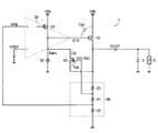
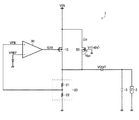
図1は、リニア電源の第1実施形態を示す図である。本実施形態のリニア電源1は、出力トランジスタ10と、出力分圧部20と、ドライバ30と、デプレッション型NMOSFET[N-channel type metal oxide semiconductor field effect transistor]40とを有し、入力電圧VINを降圧して所望の出力電圧VOUTを生成する。出力電圧VOUTは、後段の負荷2(=二次電源やマイコンなど)に供給されている。なお、出力電圧VOUTの出力端と接地端(=接地電圧0Vの印加端)との間には、出力電圧VOUTを平滑するための出力キャパシタ3を並列接続しておくとよい。リニア電源1は、例えば、IC内蔵の基準電圧源として用いることができる。
<First Embodiment>
FIG. 1 is a diagram showing a first embodiment of a linear power supply. The
出力トランジスタ10は、入力電圧VINの入力端と出力電圧VOUTの出力端との間に接続されており、ドライバ30からのゲート信号G10に応じて導通度(裏を返せばオン抵抗値)が制御される。なお、本図の例では、出力トランジスタ10として、PMOSFET[P-channel type MOSFET]が用いられている。従って、ゲート信号G10が低いほど、出力トランジスタ10の導通度が高くなり、出力電圧VOUTが上昇する。逆に、ゲート信号G10が高いほど、出力トランジスタ10の導通度が低くなり、出力電圧VOUTが低下する。
The
出力分圧部20は、出力電圧VOUTの出力端と接地端との間に直列接続された抵抗21及び22(抵抗値:R1及びR2)を含み、両抵抗相互間の接続ノードから出力電圧VOUTに応じた帰還電圧VFB(=VOUT×{R2/(R1+R2)})を出力する。ただし、出力電圧VOUTがドライバ30の入力ダイナミックレンジに収まっていれば、出力分圧部20を割愛して出力電圧VOUTをドライバ30に直接入力しても構わない。
The output
ドライバ30は、非反転入力端(+)に入力される帰還電圧VFBが反転入力端(−)に入力される所定の基準電圧VREFと一致するようにゲート信号G10を生成して出力トランジスタ10を駆動する。なお、ドライバ30は、その出力段を構成する回路要素として、PMOSFET31と電流源32を含む。
The
PMOSFET31は、入力電圧VINの入力端と出力トランジスタ10のゲートとの間に接続されており、帰還電圧VFBと基準電圧VREFとの差分値ΔV(=VFB−VREF)に応じて導通度が制御される。具体的には、差分値ΔVが高いほど、PMOSFET31の導通度が高くなり、ゲート信号G10が上昇する。逆に、差分値ΔVが低いほど、PMOSFET31の導通度が低くなり、ゲート信号G10が低下する。
The PMOSFET 31 is connected between the input end of the input voltage VIN and the gate of the
電流源32は、出力トランジスタ10のゲートと接地端との間に接続されており、ドライバ30の駆動電流Idrvを生成する。なお、リニア電源1の消費電力を低減するためには、定常的に流れるドライバ30の駆動電流Idrvをできるだけ小さく絞っておくことが望ましい。
The
デプレッション型NMOSFET40は、出力電圧VOUTの立ち上がりと共に減少するドレイン電流Idを生成し、これを起動時に増強すべき電流(本図ではドライバ30の駆動電流Idrv)に足し合わせる電流ブースターとして機能する。その接続関係について述べると、デプレッション型NMOSFET40は、ドレインがドライバ30の出力段(具体的には駆動電流Idrvを生成する電流源32の出力端)に接続されており、ソースが出力電圧VOUTの出力端に接続されており、ゲートが定電圧V1(本図では接地電圧0V)の印加端に接続されている。
The depletion type NMOSFET 40 functions as a current booster that generates a drain current Id that decreases with the rise of the output voltage VOUT and adds this to the current to be increased at startup (the drive current Idrv of the
以下では、デプレッション型NMOSFET40の導入意義について詳細に説明する。
Hereinafter, the significance of introducing the
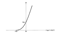
図2は、デプレッション型NMOSFET40のId−Vgs特性図である。図示のように、デプレッション型NMOSFET40は、負のオンスレッショルド電圧(=−Vth)を持っており、そのゲート・ソース間電圧Vgs(=V1−VOUT)が0Vであっても正のドレイン電流Id(いわゆるドレイン飽和電流Idss)を流すことができる。
FIG. 2 is an Id-Vgs characteristic diagram of the
上記の特性に鑑み、デプレッション型NMOSFET40を電流ブースターとして機能させるためには、出力電圧VOUTの立ち上げ開始時点(VOUT=0V)において、デプレッション型NMOSFET40のゲート・ソース間電圧Vgsがオンスレッショルド電圧(=−Vth)以上となるように、定電圧V1を適切な電圧値(例えばV1=0V)に設定しておけばよいことが分かる。
In view of the above characteristics, in order to make the
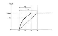
図3は、第1実施形態(V1=0V)における出力電圧VOUTの立ち上げ挙動を示すタイムチャートである。なお、本図中の実線は電流ブースターありの挙動を示しており、小破線は電流ブースターなしの挙動(従来挙動)を示している。 FIG. 3 is a time chart showing the start-up behavior of the output voltage VOUT in the first embodiment (V1 = 0V). The solid line in this figure shows the behavior with the current booster, and the small broken line shows the behavior without the current booster (conventional behavior).
時刻t1において、リニア電源1が起動すると、出力電圧VOUTが0V付近から立ち上がり始める。ここで、VOUT=0Vであるときには、デプレッション型NMOSFET40のゲート・ソース間電圧Vgs(=−VOUT)も0Vとなる。
When the
ただし、先にも述べたように、デプレッション型NMOSFET40は、負のオンスレッショルド電圧(=−Vth)を持っており、そのゲート・ソース間電圧Vgsが0Vであっても、正のドレイン電流Idを流すことができる。
However, as described above, the
従って、リニア電源1の起動時には、ドライバ30の出力段に流れる駆動電流を(Idrv+Id)まで増強することができるので、ゲート信号G10を素早く引き下げることが可能となり、延いては、出力電圧VOUTの立ち上げを高速化することが可能となる。
Therefore, when the
特に、出力トランジスタ10のゲート・ソース間に大きい寄生容量Cgsが付随している場合には、デプレッション型NMOSFET40の導入が有効となる。
In particular, when a large parasitic capacitance Cgs is attached between the gate and source of the
その後、出力電圧VOUTが上昇し、時刻t2において、デプレッション型NMOSFET40のゲート・ソース間電圧Vgs(=−VOUT)がオンスレッショルド電圧(=−Vth)よりも低くなると、デプレッション型NMOSFET40がオフするので、ドレイン電流Idがゼロ値となる。その結果、時刻t2以降、ドライバ30の出力段には、電流源32で生成される駆動電流Idrvのみが流れる状態となり、出力電圧VOUTの上昇速度(=実線の傾き)が従来挙動のそれ(=小破線の傾き)と等しくなる。
After that, when the output voltage VOUT rises and the gate-source voltage Vgs (= −VOUT) of the
なお、本図の例では、時刻t1〜t2に亘る電流ブースト動作により、リニア電源1の起動時間(=出力電圧VOUTが立ち上げ開始当初の初期値0Vから目標値Vtargetに到達するまでの所要時間)が、従来の「T1(=t4−t1)」から「T2(=t3−t1)」まで短縮されている。
In the example of this figure, the start time of the linear power supply 1 (= the time required for the output voltage VOUT to reach the target value Vtarget from the
このように、デプレッション型NMOSFET40を用いて、リニア電源1の起動時にのみ電流ブースト動作を行う構成であれば、リニア電源1の定常動作時における消費電流を不必要に増大させることなく、リニア電源1の起動時間を短縮することが可能となる。
As described above, if the
また、本実施形態のリニア電源1であれば、実績のある既存回路にデプレッション型NMOSFET40を一つ追加するだけで、上記の電流ブースト動作を実現することができる、という点も大きなメリットであると言える。
Further, the
<第2実施形態>
図4は、リニア電源の第2実施形態を示す図である。本実施形態のリニア電源1は、先出の第1実施形態(図1)をベースとしつつ、デプレッション型NMOSFET40のゲートに正の定電圧V1(>0V)を印加した構成とされている。
<Second Embodiment>
FIG. 4 is a diagram showing a second embodiment of the linear power supply. The
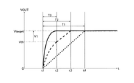
図5は、第2実施形態における出力電圧VOUTの立ち上げ挙動を示すタイムチャートである。なお、本図中の実線は第2実施形態(V1>0V)の挙動を示しており、大破線は第1実施形態(V1=0V)の挙動を示しており、小破線は電流ブースターなしの挙動(従来挙動)を示している。 FIG. 5 is a time chart showing the start-up behavior of the output voltage VOUT in the second embodiment. The solid line in this figure shows the behavior of the second embodiment (V1> 0V), the large broken line shows the behavior of the first embodiment (V1 = 0V), and the small broken line shows the behavior without the current booster. The behavior (conventional behavior) is shown.
本実施形態のリニア電源1であれば、VOUT>Vth+V1となるまで、デプレッション型NMOSFET40がオフしなくなる。すなわち、定電圧V1の電圧値に応じて、デプレッション型NMOSFET40のオフタイミングを任意に調整することができる。
With the
また、本実施形態のリニア電源1であれば、起動時におけるデプレッション型NMOSFET40のゲート・ソース間電圧Vgsが正電圧(>0V)となるので、電流ブースト動作時のドレイン電流Idが第1実施形態のそれよりも大きくなる(図2を参照)。従って、出力電圧VOUTを第1実施形態よりも迅速に立ち上げることも可能となる。
Further, in the case of the
なお、本図の例では、Vth+V1=Vtargetとなるように、定電圧V1の電圧値が設定されている。このような設定を行うことにより、出力電圧VOUTがその目標値Vtargetに到達するまで、ドレイン電流Idを流し続けることができる。従って、第1実施形態(大破線)と異なり、出力電圧VOUTの上昇途中で電流ブースト動作が終了しないので、電流ブースト動作の効果を最大限に享受することが可能となる。 In the example of this figure, the voltage value of the constant voltage V1 is set so that Vth + V1 = Vtaget. By making such a setting, the drain current Id can continue to flow until the output voltage VOUT reaches the target value Vtaget. Therefore, unlike the first embodiment (large broken line), the current boost operation does not end while the output voltage VOUT is rising, so that the effect of the current boost operation can be enjoyed to the maximum.
特に、本図の例では、定電圧V1の最適化(V1=Vtarget−Vth)により、リニア電源1の起動時間が、第1実施形態の「T2(=t3−t1)」から「T3(=t2−t1)」までさらに短縮されている。
In particular, in the example of this figure, the start-up time of the
<第3実施形態>
図6は、リニア電源の第3実施形態を示す図である。本実施形態のリニア電源1は、先の第2実施形態(図4)をベースとしつつ、出力分圧部20に抵抗23(抵抗値:R3)を追加することにより、出力電圧VOUTを分圧して生成される分圧電圧(=VOUT×{(R1+R2)/(R1+R2+R3)})を正の定電圧V1として、デプレッション型NMOSFET40のゲートに印加した構成とされている。
<Third Embodiment>
FIG. 6 is a diagram showing a third embodiment of the linear power supply. The
本構成を採用することにより、別途新たに電源を用意することなく、抵抗23を一つ追加するだけで、デプレッション型NMOSFET40のゲートに正の定電圧V1を印加することが可能となる。
By adopting this configuration, it is possible to apply a positive constant voltage V1 to the gate of the depletion type NMOSFET 40 simply by adding one
なお、本実施形態のリニア電源1では、Vgs=−α×VOUT(ただし、分圧比α={R3/(R1+R2+R3)})として表すことができる。
In the
従って、α≦Vth/Vtargetを満たすように分圧比αを設定すると、ドレイン電流Idは、遅くとも出力電圧VOUTが目標値Vtargetに到達するまでにゼロ値となる。従って、リニア電源1の定常動作時における消費電流を不要に増大せずに済む。
Therefore, if the voltage division ratio α is set so as to satisfy α ≦ Vth / Vtaget, the drain current Id becomes a zero value by the time the output voltage VOUT reaches the target value Vtaget at the latest. Therefore, it is not necessary to unnecessarily increase the current consumption during steady operation of the
逆に、α>Vth/Vtargetを満たすように分圧比αを設定すると、ドレイン電流Idは、出力電圧VOUTが目標値Vtargetに到達した後も、ゼロ値とならずに流れ続ける。このように、リニア電源1の定常動作中にデプレッション型NMOSFET40をフルオフさせる必要はなく、小さく絞られたドレイン電流Idを駆動電流Idrvに代えて(または駆動電流Idrvと共に)ドライバ30の出力段に流し続けても構わない。本構成を採用すれば、必要に応じて電流源32を割愛することができるので、リニア電源1の回路規模を縮小することが可能となる。
On the contrary, when the voltage division ratio α is set so as to satisfy α> Vth / Vtaget, the drain current Id continues to flow without becoming a zero value even after the output voltage VOUT reaches the target value Vtaget. In this way, it is not necessary to fully turn off the depletion type NMOSFET 40 during the steady operation of the
<第4実施形態>
図7は、リニア電源の第4実施形態を示す図である。本実施形態のリニア電源1は、先出の第1〜第3実施形態(図1、図4、図6)をベースとしつつ、ドライバ30の電流ブースターとして機能するデプレッション型NMOSFET40に代えて、出力トランジスタ10と並列にデプレッション型NMOSFET50を有する構成とされている。
<Fourth Embodiment>
FIG. 7 is a diagram showing a fourth embodiment of the linear power supply. The
デプレッション型NMOSFET50は、出力電圧VOUTの立ち上がりと共に減少するドレイン電流Idを生成し、これを出力電圧VOUTの出力端に流し込むことにより、出力電圧VOUTを直接的に持ち上げる出力ブースターとして機能する。その接続関係について述べると、デプレッション型NMOSFET50は、ドレインが入力電圧VINの入力端に接続されており、ソースが出力電圧VOUTの出力端に接続されており、ゲートが定電圧V1(本図では接地電圧0V)の印加端に接続されている。
The depletion type NMOSFET 50 functions as an output booster that directly raises the output voltage VOUT by generating a drain current Id that decreases with the rise of the output voltage VOUT and pouring this into the output end of the output voltage VOUT. Speaking of the connection relationship, in the
例えば、負荷2が軽い場合(=負荷2が高インピーダンスであって負荷2に流れる電流が小さい場合)には、本実施形態で示したように、デプレッション型NMOSFET50を用いて出力電圧VOUTを直接的に持ち上げることも可能である。
For example, when the
なお、本実施形態では、第1〜第3実施形態のデプレッション型NMOSFET40に代えてデプレッション型NMOSFET50を設けた構成を例に挙げたが、デプレッション型NMOSFET40及び50の双方を設けても構わない。
In this embodiment, the configuration in which the
<車両への適用>
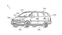
図8は、車両Xの外観図である。本構成例の車両Xは、不図示のバッテリから電源電圧の供給を受けて動作する種々の電子機器X11〜X18を搭載している。なお、本図における電子機器X11〜X18の搭載位置は、図示の便宜上、実際とは異なる場合がある。
<Application to vehicles>
FIG. 8 is an external view of the vehicle X. The vehicle X of this configuration example is equipped with various electronic devices X11 to X18 that operate by receiving a power supply voltage from a battery (not shown). The mounting positions of the electronic devices X11 to X18 in this figure may differ from the actual mounting positions for convenience of illustration.
電子機器X11は、エンジンに関連する制御(インジェクション制御、電子スロットル制御、アイドリング制御、酸素センサヒータ制御、及び、オートクルーズ制御など)を行うエンジンコントロールユニットである。 The electronic device X11 is an engine control unit that performs control related to the engine (injection control, electronic throttle control, idling control, oxygen sensor heater control, auto cruise control, etc.).
電子機器X12は、HID[high intensity discharged lamp]やDRL[daytime running lamp]などの点消灯制御を行うランプコントロールユニットである。 The electronic device X12 is a lamp control unit that controls turning on and off such as HID [high intensity discharged lamp] and DRL [daytime running lamp].
電子機器X13は、トランスミッションに関連する制御を行うトランスミッションコントロールユニットである。 The electronic device X13 is a transmission control unit that performs control related to the transmission.
電子機器X14は、車両Xの運動に関連する制御(ABS[anti-lock brake system]制御、EPS[electric power steering]制御、電子サスペンション制御など)を行う制動ユニットである。 The electronic device X14 is a braking unit that performs controls related to the movement of the vehicle X (ABS [anti-lock brake system] control, EPS [electric power steering] control, electronic suspension control, etc.).
電子機器X15は、ドアロックや防犯アラームなどの駆動制御を行うセキュリティコントロールユニットである。 The electronic device X15 is a security control unit that controls drive such as a door lock and a security alarm.
電子機器X16は、ワイパー、電動ドアミラー、パワーウィンドウ、ダンパー(ショックアブソーバー)、電動サンルーフ、及び、電動シートなど、標準装備品やメーカーオプション品として、工場出荷段階で車両Xに組み込まれている電子機器である。 The electronic device X16 is an electronic device incorporated in the vehicle X at the factory shipment stage as standard equipment such as a wiper, an electric door mirror, a power window, a damper (shock absorber), an electric sunroof, and an electric seat as a manufacturer's option. Is.
電子機器X17は、車載A/V[audio/visual]機器、カーナビゲーションシステム、及び、ETC[electronic toll collection system]など、ユーザオプション品として任意で車両Xに装着される電子機器である。 The electronic device X17 is an electronic device that is optionally mounted on the vehicle X as a user option such as an in-vehicle A / V [audio / visual] device, a car navigation system, and an ETC [electronic toll collection system].
電子機器X18は、車載ブロア、オイルポンプ、ウォーターポンプ、バッテリ冷却ファンなど、高耐圧系モータを備えた電子機器である。 The electronic device X18 is an electronic device provided with a high withstand voltage motor such as an in-vehicle blower, an oil pump, a water pump, and a battery cooling fan.
なお、先に説明したリニア電源1は、電子機器X11〜X18のいずれにも組み込むことが可能である。
The
<その他の変形例>
なお、本明細書中に開示されている種々の技術的特徴は、上記実施形態のほか、その技術的創作の主旨を逸脱しない範囲で種々の変更を加えることが可能である。すなわち、上記実施形態は、全ての点で例示であって制限的なものではないと考えられるべきであり、本発明の技術的範囲は、上記実施形態の説明ではなく、特許請求の範囲によって示されるものであり、特許請求の範囲と均等の意味及び範囲内に属する全ての変更が含まれると理解されるべきである。
<Other variants>
In addition to the above-described embodiment, various technical features disclosed in the present specification can be modified in various ways without departing from the spirit of the technical creation. That is, it should be considered that the above-described embodiment is exemplary in all respects and is not restrictive, and the technical scope of the present invention is shown not by the description of the above-mentioned embodiment but by the scope of claims. It should be understood that it includes all changes that fall within the meaning and scope of the claims.
本明細書中に開示されている発明は、車両関連機器、船舶関連機器、事務機器、ポータブル機器、ないしは、スマートフォンなどに利用することが可能である。 The invention disclosed in the present specification can be used for vehicle-related equipment, ship-related equipment, office equipment, portable equipment, smartphones, and the like.
1 リニア電源
2 負荷
3 出力キャパシタ
10 出力トランジスタ(PMOSFET)
20 出力分圧部
21、22、23 抵抗
30 ドライバ
31 PMOSFET
32 電流源
40、50 デプレッション型NMOSFET
X 車両
X11〜X18 電子機器
1
20
32
X Vehicle X11-X18 Electronic Equipment
Claims (10)
前記入力電圧の入力端と前記出力電圧の出力端との間に接続された出力トランジスタと、
前記出力電圧またはこれに応じた帰還電圧が所定の基準電圧と一致するように前記出力トランジスタを駆動するドライバと、
負のオンスレッショルド電圧を持ち、前記リニア電源の起動時に前記出力電圧が0Vであってもオンして前記出力電圧の立ち上がりと共に減少するドレイン電流を生成し、前記ドレイン電流を前記リニア電源の起動時間を短縮するために増強すべき電流に足し合わせるデプレッション型NMOSFETと、
を有することを特徴とするリニア電源。 A linear power supply configured to step down the input voltage to generate an output voltage.
And an output transistor connected between an output terminal of the input terminal and the output voltage of said input voltage,
A driver that drives the output transistor so that the output voltage or the feedback voltage corresponding thereto matches a predetermined reference voltage.
It has a negative on-threshold voltage, and even if the output voltage is 0V when the linear power supply is started, it turns on to generate a drain current that decreases with the rise of the output voltage, and the drain current is used as the start-up time of the linear power supply. Depression type MOSFET that adds to the current that should be increased in order to shorten
A linear power supply characterized by having.
前記入力電圧の入力端と前記出力電圧の出力端との間に接続された出力トランジスタと、
前記出力電圧またはこれに応じた帰還電圧が所定の基準電圧と一致するように前記出力トランジスタを駆動するドライバと、
負のオンスレッショルド電圧を持ち、前記リニア電源の起動時に前記出力電圧が0Vであってもオンして前記出力電圧の立ち上がりと共に減少するドレイン電流を生成し、前記ドレイン電流を前記出力電圧の出力端に流し込むデプレッション型NMOSFETと、
を有することを特徴とするリニア電源。 A linear power supply configured to step down the input voltage to generate an output voltage.
And an output transistor connected between an output terminal of the input terminal and the output voltage of said input voltage,
A driver that drives the output transistor so that the output voltage or the feedback voltage corresponding thereto matches a predetermined reference voltage.
Has a negative on-threshold voltage, the linear supply the output voltage during startup of generating a drain current which decreases with a rise of the output voltage is turned on even 0V, the output terminal of the output voltage of the drain current Depression type MOSFET to pour into
A linear power supply characterized by having.
Priority Applications (2)
| Application Number | Priority Date | Filing Date | Title |
|---|---|---|---|
| JP2017003944A JP6835599B2 (en) | 2017-01-13 | 2017-01-13 | Linear power supply |
| US15/868,083 US10359795B2 (en) | 2017-01-13 | 2018-01-11 | Linear power source |
Applications Claiming Priority (1)
| Application Number | Priority Date | Filing Date | Title |
|---|---|---|---|
| JP2017003944A JP6835599B2 (en) | 2017-01-13 | 2017-01-13 | Linear power supply |
Publications (2)
| Publication Number | Publication Date |
|---|---|
| JP2018112962A JP2018112962A (en) | 2018-07-19 |
| JP6835599B2 true JP6835599B2 (en) | 2021-02-24 |
Family
ID=62841380
Family Applications (1)
| Application Number | Title | Priority Date | Filing Date |
|---|---|---|---|
| JP2017003944A Active JP6835599B2 (en) | 2017-01-13 | 2017-01-13 | Linear power supply |
Country Status (2)
| Country | Link |
|---|---|
| US (1) | US10359795B2 (en) |
| JP (1) | JP6835599B2 (en) |
Families Citing this family (3)
| Publication number | Priority date | Publication date | Assignee | Title |
|---|---|---|---|---|
| JP2020135372A (en) * | 2019-02-19 | 2020-08-31 | ローム株式会社 | Power supply circuit |
| JP7271227B2 (en) * | 2019-02-27 | 2023-05-11 | ローム株式会社 | power circuit |
| CN113157040B (en) * | 2021-04-28 | 2022-07-12 | 晋江三伍微电子有限公司 | Low dropout linear voltage stabilizing circuit and electronic equipment |
Family Cites Families (3)
| Publication number | Priority date | Publication date | Assignee | Title |
|---|---|---|---|---|
| JP2014038541A (en) | 2012-08-20 | 2014-02-27 | Yamaha Corp | Power supply circuit including regulator |
| JP6261343B2 (en) * | 2013-03-06 | 2018-01-17 | エスアイアイ・セミコンダクタ株式会社 | Voltage regulator |
| JP6316632B2 (en) * | 2014-03-25 | 2018-04-25 | エイブリック株式会社 | Voltage regulator |
-
2017
- 2017-01-13 JP JP2017003944A patent/JP6835599B2/en active Active
-
2018
- 2018-01-11 US US15/868,083 patent/US10359795B2/en active Active
Also Published As
| Publication number | Publication date |
|---|---|
| US10359795B2 (en) | 2019-07-23 |
| JP2018112962A (en) | 2018-07-19 |
| US20180203477A1 (en) | 2018-07-19 |
Similar Documents
| Publication | Publication Date | Title |
|---|---|---|
| JP7177661B2 (en) | linear power supply circuit | |
| US10067520B2 (en) | Linear power supply circuit | |
| JP6510828B2 (en) | LINEAR POWER SUPPLY AND ELECTRONIC DEVICE USING THE SAME | |
| JP6893788B2 (en) | Linear power supply | |
| JP6835599B2 (en) | Linear power supply | |
| JP7295881B2 (en) | linear power supply circuit | |
| JP7230249B2 (en) | linear power supply circuit | |
| US11262777B2 (en) | Power supply circuit, power supply device, and motor vehicle including the same | |
| US11068003B2 (en) | Differential amplifier | |
| JP2020099139A (en) | Switching device | |
| JP2021033472A (en) | Linear power supply | |
| JP6830364B2 (en) | Soft start circuit and power supply equipped with this | |
| US11586235B2 (en) | Linear power supply circuit with phase compensation circuit | |
| US20230198401A1 (en) | Switch control circuit, voltage output device, and vehicle | |
| JP7139142B2 (en) | switch device |
Legal Events
| Date | Code | Title | Description |
|---|---|---|---|
| A621 | Written request for application examination |
Free format text: JAPANESE INTERMEDIATE CODE: A621 Effective date: 20191218 |
|
| A977 | Report on retrieval |
Free format text: JAPANESE INTERMEDIATE CODE: A971007 Effective date: 20200930 |
|
| A131 | Notification of reasons for refusal |
Free format text: JAPANESE INTERMEDIATE CODE: A131 Effective date: 20201013 |
|
| A521 | Request for written amendment filed |
Free format text: JAPANESE INTERMEDIATE CODE: A523 Effective date: 20201209 |
|
| TRDD | Decision of grant or rejection written | ||
| A01 | Written decision to grant a patent or to grant a registration (utility model) |
Free format text: JAPANESE INTERMEDIATE CODE: A01 Effective date: 20210126 |
|
| A61 | First payment of annual fees (during grant procedure) |
Free format text: JAPANESE INTERMEDIATE CODE: A61 Effective date: 20210204 |
|
| R150 | Certificate of patent or registration of utility model |
Ref document number: 6835599 Country of ref document: JP Free format text: JAPANESE INTERMEDIATE CODE: R150 |
|
| R250 | Receipt of annual fees |
Free format text: JAPANESE INTERMEDIATE CODE: R250 |