JP6828058B2 - Magnetic Resonance Imaging Cryogenic magnetic field sensing to compensate for magnetic field fluctuations in magnets - Google Patents
Magnetic Resonance Imaging Cryogenic magnetic field sensing to compensate for magnetic field fluctuations in magnets Download PDFInfo
- Publication number
- JP6828058B2 JP6828058B2 JP2018563821A JP2018563821A JP6828058B2 JP 6828058 B2 JP6828058 B2 JP 6828058B2 JP 2018563821 A JP2018563821 A JP 2018563821A JP 2018563821 A JP2018563821 A JP 2018563821A JP 6828058 B2 JP6828058 B2 JP 6828058B2
- Authority
- JP
- Japan
- Prior art keywords
- superconducting
- magnetic field
- magnet
- coil
- compensation
- Prior art date
- Legal status (The legal status is an assumption and is not a legal conclusion. Google has not performed a legal analysis and makes no representation as to the accuracy of the status listed.)
- Expired - Fee Related
Links
Images


Classifications
-
- G—PHYSICS
- G01—MEASURING; TESTING
- G01R—MEASURING ELECTRIC VARIABLES; MEASURING MAGNETIC VARIABLES
- G01R33/00—Arrangements or instruments for measuring magnetic variables
- G01R33/20—Arrangements or instruments for measuring magnetic variables involving magnetic resonance
- G01R33/28—Details of apparatus provided for in groups G01R33/44 - G01R33/64
- G01R33/38—Systems for generation, homogenisation or stabilisation of the main or gradient magnetic field
- G01R33/389—Field stabilisation, e.g. by field measurements and control means or indirectly by current stabilisation
-
- G—PHYSICS
- G01—MEASURING; TESTING
- G01R—MEASURING ELECTRIC VARIABLES; MEASURING MAGNETIC VARIABLES
- G01R33/00—Arrangements or instruments for measuring magnetic variables
- G01R33/20—Arrangements or instruments for measuring magnetic variables involving magnetic resonance
- G01R33/28—Details of apparatus provided for in groups G01R33/44 - G01R33/64
- G01R33/38—Systems for generation, homogenisation or stabilisation of the main or gradient magnetic field
- G01R33/381—Systems for generation, homogenisation or stabilisation of the main or gradient magnetic field using electromagnets
- G01R33/3815—Systems for generation, homogenisation or stabilisation of the main or gradient magnetic field using electromagnets with superconducting coils, e.g. power supply therefor
-
- G—PHYSICS
- G01—MEASURING; TESTING
- G01R—MEASURING ELECTRIC VARIABLES; MEASURING MAGNETIC VARIABLES
- G01R33/00—Arrangements or instruments for measuring magnetic variables
- G01R33/20—Arrangements or instruments for measuring magnetic variables involving magnetic resonance
- G01R33/28—Details of apparatus provided for in groups G01R33/44 - G01R33/64
- G01R33/42—Screening
- G01R33/421—Screening of main or gradient magnetic field
-
- H—ELECTRICITY
- H01—ELECTRIC ELEMENTS
- H01F—MAGNETS; INDUCTANCES; TRANSFORMERS; SELECTION OF MATERIALS FOR THEIR MAGNETIC PROPERTIES
- H01F6/00—Superconducting magnets; Superconducting coils
- H01F6/006—Supplying energising or de-energising current; Flux pumps
Landscapes
- Physics & Mathematics (AREA)
- Condensed Matter Physics & Semiconductors (AREA)
- General Physics & Mathematics (AREA)
- Engineering & Computer Science (AREA)
- Power Engineering (AREA)
- Health & Medical Sciences (AREA)
- Epidemiology (AREA)
- Electromagnetism (AREA)
- Magnetic Resonance Imaging Apparatus (AREA)
Description
本願は、一般に、超伝導磁石技術、及びそれを使用する磁気共鳴イメージング及び分光技術に関する。 The present application generally relates to superconducting magnet technology and magnetic resonance imaging and spectroscopic techniques using it.
磁気共鳴(MR)イメージングは、経時的に安定している静磁場から利益を得る。MRIスキャナの主(又は静)磁場は、一般にB0磁場と表され、核スピンを整列させる(統計的意味で)ために高い値を有する。医用イメージングで使用されるいくつかのMRスキャナでは、B0は0.2テスラから3.0テスラの範囲にあり、さらに高い値、例えばB0=7テスラが研究用途で使用される。これらの高い磁場を達成するために、超伝導磁石が一般に使用される。超伝導磁石巻線を製作するのに好適ないくつかの超伝導材料には、一般に20Kより低い臨界温度(TC)を有するニオブチタン、ニオブ−スズなどが含まれる。それにより、超伝導磁石巻線は、適切に低い極低温に巻線を維持するために、真空ジャケット付きLHeデュワーに収容されている液体ヘリウム(LHe)に浸されるか、又は他のタイプのクライオスタットに配置される。より高いTCをもつ超伝導材料を使用する磁石では、磁石クライオスタットは、液体窒素(LN2)又は真空に浸されるなどの他の形態を取ることができる。 Magnetic resonance (MR) imaging benefits from a static magnetic field that is stable over time. The main (or static) magnetic field of an MRI scanner is commonly referred to as the B0 magnetic field and has a high value for aligning nuclear spins (in a statistical sense). In some MR scanners used in medical imaging, B 0 is in the range of 0.2 Tesla to 3.0 Tesla, and higher values such as B 0 = 7 Tesla are used for research purposes. Superconducting magnets are commonly used to achieve these high magnetic fields. Some superconducting material suitable for fabricating the superconducting magnet windings, generally niobium titanium having a low critical temperature (T C) than 20K, niobium -, and the like tin. Thereby, the superconducting magnet winding is immersed in liquid helium (LHe) contained in a vacuum jacketed LHe dewar, or of any other type, in order to maintain the winding at an appropriately low cryogenic temperature. Placed on the cryostat. The magnet using the superconducting material having a higher T C, magnet cryostat may take other forms, such as immersed in liquid nitrogen (LN 2) or a vacuum.
しかしながら、ほんの数nTの程度の小さな時間的B0変動がMR画像品質を劣化させる可能性がある。典型的な医用イメージング用途で許容されるnT変動の量は、周波数に依存しており、0.01から100Hzにおいて約1から100nTの範囲である。したがって、許容できる変動は、10億分の1(ppb)の範囲にある。これよりも大きいB0変動は、MRスキャナのまわりの外部源、例えば、スキャナの近傍の電気線路、又は列車、自動車、エレベータのような移動する磁性物体などによって容易に引き起こされる。それゆえに、MR磁石は、一般に、良好な画質を得るために外部磁場変動を補償するように装備される。そのような装備は、本明細書ではB0補償システムと呼ばれる。B0補償システムの設計目標は、一般に、外部B0磁場外乱を1/10から1/100に減少させることである。B0磁場外乱低減率は、本明細書では遮蔽率と呼ばれ、より高い遮蔽率はより良好なB0補償に対応する。(「外部」B0磁場は、磁石自体の外側のB0磁場を指し、一般に、イメージング視野(FOV)における、例えば、水平ボアタイプMRスキャナのボアのアイソセンタにおけるB0磁場を指す)。 However, small time B 0 fluctuations in the degree of few nT might degrade the MR image quality. The amount of nT variation allowed in typical medical imaging applications is frequency dependent and ranges from about 1 to 100 nT at 0.01 to 100 Hz. Therefore, the permissible variation is in the parts per billion (ppb). Larger B0 fluctuations are easily caused by external sources around the MR scanner, such as electrical tracks near the scanner, or moving magnetic objects such as trains, automobiles, and elevators. Therefore, MR magnets are generally equipped to compensate for external magnetic field fluctuations in order to obtain good image quality. Such equipment is referred to herein as B 0 compensation system. Design goal of B 0 compensation system, generally, it is to reduce the external B 0 magnetic field disturbance from 1/10 to 1/100. The B 0 magnetic field disturbance reduction rate is referred to herein as the shielding rate, and a higher shielding rate corresponds to a better B 0 compensation. ( "External" B 0 magnetic field, points outside the B 0 field of the magnet itself, generally refers in imaging field of view (FOV), for example, the B 0 magnetic field at the isocenter of the horizontal bore-type MR scanner bore).
様々なタイプのB0補償システムが開発されている。能動補償手法では、磁場センサが、イメージングFOVに又はその近くに設置され、測定された磁場が、B0磁場外乱を能動的に阻止するためのフィードバック制御で使用される。B0変動を能動的に補償する1つのやり方は、能動的に補償磁場を印加するものである。例えば、制御電子機器が1つ又は複数のコイルを駆動して、磁石のところに補償磁場を発生する。代替として、磁気共鳴周波数は磁場に比例する(磁気回転比が比例定数となる)ので、能動補償は、測定されたMR信号に実行される(例えばソフトウェアで)周波数調節とすることができる。 Various types of B0 compensation systems have been developed. In active compensation technique, the magnetic field sensor is installed in the imaging FOV or near, the measured magnetic field is used in a feedback control to actively prevent the B 0 field disturbance. One method of actively compensating for B 0 fluctuations is to actively apply a compensating magnetic field. For example, a control electronic device drives one or more coils to generate a compensating magnetic field at a magnet. Alternatively, the magnetic resonance frequency is proportional to the magnetic field (the gyromagnetic ratio is a constant of proportionality), so active compensation can be a frequency adjustment performed on the measured MR signal (eg, in software).
他のタイプのB0補償システムは、受動的であり、超伝導磁石巻線とともに配置された超伝導回路を磁石クライオスタットに追加することを必要とする。いくつかの受動B0補償システムが、例えば、Reichert、米国特許第4,926,289号(「Actively shielded, superconducting magnet of an NMR tomography apparatus」)及びOverweg、米国特許第5,426,366号(「Magnetic resonance apparatus comprising a superconducting magnet」)に記載されている。これらの構想は、超伝導回路が磁束を一定に保つという原理に基づいている。1つの構想では、B0補償回路は、磁石巻線に電気的に接続され、その接続は、戦略的に選ばれた場所、一般に巻線コイル内で行われる。接続点を適切に設計することによって、100を超える遮蔽率を得ることが可能である。代替の設計では、B0補償回路の巻線の磁石巻線との磁気結合が、電気接続の代わりに用いられる。この場合もまた、適切な結合設計により、100を超える遮蔽率が準DC外乱に対して得られる。 Other types of B0 compensation systems are passive and require the addition of superconducting circuits placed with the superconducting magnet windings to the magnet cryostat. Several passive B 0 compensation system, for example, Reichert, U.S. Patent No. 4,926,289 ( "Actively shielded, superconducting magnet of an NMR tomography apparatus ") and Overweg, U.S. Patent No. 5,426,366 ( It is described in "Magnetic resonance application patents comprising a superconducting system"). These concepts are based on the principle that superconducting circuits keep magnetic flux constant. In one concept, B 0 compensation circuit is electrically connected to the magnet windings, the connection, the location chosen for strategic, is generally carried out at a winding coil. By properly designing the connection points, it is possible to obtain a shielding rate of more than 100. In an alternative design, the magnetic coupling between the magnet winding of the windings of the B 0 compensation circuit is used in place of the electrical connection. Again, with proper coupling design, a shielding rate greater than 100 can be obtained for quasi-DC disturbances.
本明細書では、これらの既存のB0補償システムにはいくつかの欠点があることが認識されている。能動B0補償の場合には、磁場センサをイメージングFOVの近くに(及び好ましくはイメージングFOVに対して対称に)位置づけることの困難さなどの要因に起因して、十分に正確なB0測定値(ppb範囲の精度)を得ることが困難である。受動B0補償の場合には、利得は、固定されており、あまり均一でない外乱源に対して調節することができない。準DCでない外乱を補償することも一般に実現可能でない。このタイプの外乱は固定した周波数応答を有する。磁石の金属クライオスタットは、受動B0補償システムの応答に影響を及ぼす。これは、補償が受動的であり調節できないので、補正することができない。MR磁石に電気的に接続された受動B0補償システムの場合には、最適な接続点は、通常、MR磁石のコイル巻線の内部にあり、コイルに余分なリードインリードアウト接続を必要とし、これは、製造コスト及び複雑さを付加する。MR磁石に誘導的に結合する受動B0補償システムの場合には、補償回路は余分に巻かれた超伝導コイルを必要とし、それは、遮蔽率設計基準(例えば、設計によっては少なくとも100の遮蔽率)を満たすように設計されなければならず、それは、この場合もやはり、コスト及び製造複雑さを増加させる。 It is recognized herein that these existing B0 compensation systems have some drawbacks. In the case of active B 0 compensation, sufficiently accurate B 0 measurements due to factors such as difficulty in positioning the magnetic field sensor near (and preferably symmetrical with respect to the imaging FOV) the imaging FOV. It is difficult to obtain (accuracy in the ppb range). In the case of passive B 0 compensation gain is fixed and can not be adjusted with respect to the disturbance source not very uniform. Compensating for non-quasi-DC disturbances is also generally not feasible. This type of disturbance has a fixed frequency response. Metal cryostat magnet affects the response of the passive B 0 compensation system. This cannot be corrected because the compensation is passive and cannot be adjusted. In the case of electrically connected passive B 0 compensation system in MR magnets, optimum connection point is normally located inside of the coil winding of the MR magnet, it requires extra lead-lead-out connected to the coil , This adds manufacturing cost and complexity. In the case of passive B 0 compensation system for inductively coupled to the MR magnet, the compensation circuit requires a superconducting coil extra wound, it is shielding ratio design criteria (e.g., blocking rate of at least 100 depending on the design ) Must be designed, which again increases cost and manufacturing complexity.
以下は、上記の問題などに対処する新しい改善されたシステム及び方法を開示する。 The following discloses new and improved systems and methods to address the above issues and the like.
1つの開示される態様では、超伝導磁石は、磁石クライオスタットと、磁石クライオスタットの内部に配置され、電流が超伝導磁石コイルに流れるとき静(B0)磁場を発生するように構成された超伝導磁石コイルと、磁石クライオスタットの内部に配置され、超伝導磁石コイルによって発生されるB0磁場の時間的変動を低減するために超伝導磁石コイルに結合された超伝導B0補償回路と、磁石クライオスタットの内部に配置され、超伝導B0補償回路に流れる電流を測定するように接続された電流センサとを含む。 In one disclosed embodiment, the superconducting magnet is located inside a magnet cryostat and a superconducting magnet that is configured to generate a static (B 0 ) magnetic field when an electric current flows through the superconducting magnet coil. a magnet coil, placed inside the magnet cryostat, the superconducting B 0 compensation circuit coupled to the superconducting magnet coil in order to reduce the temporal variation in the B 0 magnetic field generated by superconducting magnet coils, the magnet cryostat Includes a current sensor located inside the magnet and connected to measure the current flowing through the superconducting B0 compensation circuit.
別の開示される態様では、超伝導磁石を動作させる方法が開示される。この方法は、磁石クライオスタットを使用して、超伝導磁石コイルと、超伝導磁石コイルに結合された超伝導B0補償回路とを冷却するステップと、超伝導磁石コイルに電気的にエネルギーを与えて静(B0)磁場を発生するステップと、超伝導B0補償回路を使用してB0磁場の時間的変動を低減するステップと、磁石クライオスタットの内部に配置された電流センサを使用して、超伝導B0補償回路に流れる電流を測定するステップと、超伝導B0補償回路に流れる測定された電流に基づいて能動B0補償(及び/又はソース位置の先験的知識による傾斜補償)を実行するステップとを有する。 In another disclosed aspect, a method of operating a superconducting magnet is disclosed. This method uses a magnet cryostat, giving a superconducting magnet coil, and cooling the superconducting B 0 compensation circuit coupled to the superconducting magnet coil, the electrical energy in the superconducting magnet coil Using a step to generate a static (B 0 ) magnetic field, a step to reduce the temporal fluctuation of the B 0 magnetic field using a superconducting B 0 compensation circuit, and a current sensor located inside the magnet cryostat, measuring the current flowing through the superconducting B 0 compensation circuit, an active B 0 compensation based on the measured current flowing through the superconducting B 0 compensation circuit (and / or tilt compensation by a priori knowledge of the source location) Has steps to perform.
別の開示される態様では、磁気共鳴(MR)イメージングデバイスが開示される。超伝導磁石は、磁石クライオスタットと、磁石クライオスタットの内部に配置された超伝導磁石コイルと、磁石クライオスタットの内部に配置され、超伝導磁石コイルに結合された超伝導B0補償回路と、磁石クライオスタットの内部に配置され、超伝導B0補償回路に流れる電流を測定するように接続された電流センサとを含む。能動B0補償コンポーネントは、超伝導B0補償回路に流れる電流の測定値を受け取るために電流センサに動作可能に接続される。能動B0補償コンポーネントは、超伝導B0補償回路に流れる電流に基づいて能動B0磁場補償を行うように構成される。 In another disclosed embodiment, a magnetic resonance (MR) imaging device is disclosed. Superconducting magnet, a magnet cryostat, the superconducting magnet coils disposed in the interior of the magnet cryostat is disposed inside the magnet cryostat, the superconducting B 0 compensation circuit coupled to the superconducting magnet coil, the magnet cryostat Includes a current sensor located internally and connected to measure the current flowing through the superconducting B0 compensation circuit. The active B 0 compensation component is operably connected to the current sensor to receive a measurement of the current flowing through the superconducting B 0 compensation circuit. The active B 0 compensation component is configured to perform active B 0 magnetic field compensation based on the current flowing through the superconducting B 0 compensation circuit.
1つの利点は、製造コストを低減したB0補償システムを提供することにある。 One advantage is to provide a B0 compensation system with reduced manufacturing costs.
別の利点は、設計制約が緩和されたB0補償システムを提供することにある。 Another advantage is to provide a B0 compensation system with relaxed design constraints.
別の利点は、イメージング視野(FOV)に又はそれに隣接して磁場センサを設置する必要なしに、能動感知を有するB0補償システムを提供することにある。 Another advantage is to provide a B0 compensation system with active sensing without the need to install a magnetic field sensor in or adjacent to the imaging field of view (FOV).
別の利点は、能動B0補償を行うために外部磁場センサの代用として受動超伝導B0補償回路を相乗的に活用するB0補償システムを提供することにある。 Another advantage is to provide a B 0 compensation system that synergistically utilizes a passive superconducting B 0 compensation circuit as a substitute for an external magnetic field sensor to perform active B 0 compensation.
別の利点は、粗いB0補償を行うための受動超伝導B0補償回路と、能動B0補償の追加の成分を供給する極低温磁場センサとを相乗的に活用するB0補償システムを提供することにある。 Another advantage is that it provides a B 0 compensation system that synergistically utilizes a passive superconducting B 0 compensation circuit for coarse B 0 compensation and a cryogenic magnetic field sensor that supplies additional components of active B 0 compensation. To do.
別の利点は、磁場センサが磁石クライオスタットの内部に設置されており、したがって、外部に置かれた磁場センサと比較して熱センサ雑音が低減されたB0補償システムを提供することにある。 Another advantage is that the magnetic field sensor is installed inside the magnet cryostat, thus providing a B0 compensation system with reduced thermal sensor noise compared to an externally placed magnetic field sensor.
所与の実施形態は、本開示を読み理解すると当業者には明らかになるように、上記の利点のどれも提供しないか、上記の利点のうちの1つ、2つ、さらに多く、又はすべてを提供し、及び/又は他の利点を提供する。 A given embodiment does not provide any of the above advantages, or one, two, more, or all of the above advantages, as will become apparent to those skilled in the art upon reading and understanding the present disclosure. And / or provide other benefits.
本発明は、様々なコンポーネント及びコンポーネントの構成の形態、並びに様々なステップ及びステップの構成の形態をとる。図面は、単に好ましい実施形態を説明するためのものであり、本発明を限定するものとして解釈されるべきでない。特に明記しない限り、図面は、概略であり、原寸に比例している又は異なるコンポーネントの相対的寸法を説明するものと解釈されるべきでない。 The present invention takes various components and forms of component configuration, as well as various steps and steps. The drawings are merely intended to illustrate preferred embodiments and should not be construed as limiting the invention. Unless otherwise stated, drawings are schematic and should not be construed as describing the relative dimensions of components that are proportional to or different from their original size.
本明細書で開示するB0補償デバイス実施形態では、超伝導B0補償回路は、磁石クライオスタットの内部に配置された極低温電流センサと相乗的に組み合わされる。極低温電流センサは、超伝導B0補償回路に流れる電流を感知する。極低温電流センサは、超伝導B0補償回路によって行われる粗いB0補償に加えて能動B0補償を実行するための磁場センサの代用品として働く。別の見方をすると、受動超伝導B0補償回路は、受動B0補償を行う通常の機能に加えて、補正されるべき外乱の能動補償を実行するための代用磁場センサの追加の役割を果たす。 The B 0 compensation device embodiments disclosed herein, the superconducting B 0 compensation circuit is synergistically combined with the cryogenic current sensor arranged in the interior of the magnet cryostat. The cryogenic current sensor senses the current flowing through the superconducting B0 compensation circuit. The cryogenic current sensor acts as a substitute for a magnetic field sensor to perform active B 0 compensation in addition to the coarse B 0 compensation provided by the superconducting B 0 compensation circuit. From another viewpoint, the passive superconducting B 0 compensation circuit, in addition to the normal function of performing passive B 0 compensation, additional role of surrogate field sensors for performing active compensation of disturbance to be corrected ..
そのような構成には本質的な利点がある。超伝導B0補償回路の設計及び製造許容範囲は、超伝導B0補償回路が部分的な遮蔽(すなわち、粗いB0補償)しか実行しないのでそれほど重要でない。実効遮蔽率は、超伝導B0補償回路からの受動補償と、測定電流(能動補償で通常使用されるB0磁場測定の代用として役立つ)に基づいて行われる能動補償との組合せによって達成される。これにより、超伝導B0補償回路の設計及び製造のコストの低減が可能になる。別の利点は、遮蔽率が利得並びに周波数応答で調節され、それによって、性能の改善が可能になることである。また別の利点は、多重巻きソレノイドコイルによる磁束変換及び/又は磁石クライオスタットの内部のB0磁場に対する磁場センサの適切な方位を使用して、磁場センサにより測定された磁場を外乱源磁場に比べて増幅することができるので、極低温電流センサがソレノイドコイル/磁場センサを使用して高感度を提供できることである。加えて、極低温電流センサは、設計に関係なく、低温で動作するので固有熱雑音が低下する。さらにまた別の利点は、能動B0補償のために通常使用され、イメージング視野(FOV)に又はそれに隣接して設置されなければならない磁場センサが、磁石クライオスタットの内部に置かれた電流センサと取り替えられ、それにより、イメージングFOV内又はその近くの貴重な空間が解放されることである。 Such a configuration has essential advantages. Design and manufacturing tolerance of superconducting B 0 compensation circuit superconducting B 0 compensation partial shielding (i.e., coarse B 0 compensation) is not so important because it does not only perform. The effective shielding ratio is achieved by the combination of the active compensation is performed based on a passive compensation from superconducting B 0 compensation circuit, the measured current (serve as a substitute for the active compensation in the B 0 field measurements commonly used) .. This makes it possible to reduce the cost of designing and manufacturing the superconducting B0 compensation circuit. Another advantage is that the shielding factor is regulated by the gain as well as the frequency response, which allows for improved performance. Another advantage is to use the proper orientation of the magnetic field sensor with respect to the interior of the B 0 magnetic field flux conversion and / or magnet cryostat according multi-turn solenoid coil, as compared to the magnetic field measured by the magnetic field sensor to the disturbance source field Being able to amplify, the cryogenic current sensor can provide high sensitivity using a solenoid coil / magnetic field sensor. In addition, the cryogenic current sensor operates at low temperatures, regardless of design, thus reducing intrinsic thermal noise. Yet another advantage is normally used for active B 0 compensation, the magnetic field sensor that must be placed adjacent to or in the imaging field-of-view (FOV) is replaced with a current sensor placed in the interior of the magnet cryostat This frees up valuable space in or near the imaging FOV.
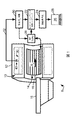
図1を参照すると、例示の磁気共鳴(MR)イメージングデバイス8は、磁石クライオスタット12に配置された超伝導磁石10を含む。磁石クライオスタット12は、超電導臨界温度より低い温度に磁石10の超伝導コイルを維持する。超伝導磁石コイルを製作するのに好適ないくつかの例示の超伝導材料には、一般に20Kより低い臨界温度(TC)を有するニオブチタン、ニオブ−スズなどが含まれる。いくつかの実施形態において、磁石クライオスタット12は真空ジャケット付き液体ヘリウム(LHe)デュワーを含み、磁石コイルは、適切に低い極低温に巻線を維持するためにLHeデュワーの内部のLHeに浸される。しかしながら、他の磁石クライオスタット設計、例えば、TCより低い温度に維持された真空空間に磁石コイルが配置される設計が考えられる。例示の実施形態では、磁石10は、水平ボア14を画定する水平ソレノイド超伝導磁石10である。水平ボア14の中に、患者又は他のイメージング対象者が、コーチ又は他の患者支持器16上に載った後MRイメージング及び/又は分光のために入れられる。これは単に例示の実施形態であり、他の超伝導磁石設計、例えば、垂直ボア磁石が考えられる。
Referring to FIG. 1, the exemplary magnetic resonance (MR) imaging device 8 includes a
超伝導磁石10は、図1に示すような静(B0)磁場を発生する。例示の水平ボア設計では、B0ベクトルは水平方向を向いているが、他の方位が磁石設計に応じて使用されてもよい。静(B0)磁場は、時間的に一定である(MRイメージングデバイス8を稼働にするときの初期ランプアップの間以外、又はメンテナンスなどのためのランプダウンの間以外)ように意図されており、一般に、強磁場であり、例えば、いくつかの設計では範囲0.2〜7.0テスラの大きさ|B0|を有するが、より高い又はより低い磁場強度も考えられる。例示のMRイメージングデバイス8は、高周波(RF)コイル18をさらに含み、高周波(RF)コイル18は、例示の実施形態では、円筒状ホールボディバードケージコイルであるが、横電磁(TEM)RFコイルなどの他の設計が使用されてもよい。加えて、例示の単一ホールボディRFコイル18は、1つ又は複数の局所RFコイルと取り替えられるか又はそれにより補足されてもよく、例えば、別の非限定の事例として、ホールボディRFコイルは対象者のMRを励起するために送信コイルとして使用されてもよく、個別の局所受信コイル、フェーズドアレイコイルアレイなどが、MR信号受信器として使用されてもよい。RFコイルの選ばれた構成は、送信/受信(Tx/Rx)電子機器20、例えば、イメージング対象者に磁気共鳴を発生させるために磁気共鳴周波数(本明細書ではf0として表す)でRFコイルを励起するように調整された無線周波数送信器によって駆動され、RF受信電子機器がMR信号を受信する。図1は概略であり、MRイメージングデバイスは、一般に、図1に示されていない多数の他の従来のコンポーネント、例えば、MR信号を操作し及び/又は空間的に符号化するための抵抗性傾斜磁場コイルなどを含む。
The
MRイメージングシステム8は、MRイメージング及び/又は分光データを取得するために知られたやり方で適切に使用される。例えば、1つの例示のイメージングシーケンスにおいて、稼働中の超伝導磁石10は、ボア14内のイメージングFOVに静(B0)磁場を生成する。B0磁場は、核スピンを(統計的に)配向させる。核スピンは、RFシステム18、20により印加されたRFパルスによって励起される。励起された磁気共鳴は、傾斜磁場コイル(図示せず)により印加された傾斜磁場によって空間的に制限され、及び/又は位相及び/又は周波数符号化され、このように操作された励起磁気共鳴は、RFシステム18、20によって検出され、MRイメージングデータ取得ハードウェア22によって処理されて、MRイメージングデータが発生される。取得ハードウェア22は、例えば、RFトランシーバ20(又はRFトランシーバ20がアナログ出力を生成する場合、アナログ−デジタル変換回路を含む)からのデジタル化MR信号を受信し、オプションとして、周波数及び/又は位相調節又は補正、k空間データとしてのフォーマットなどのMR信号への前処理を実行するようにプログラムされたコンピュータを含む。取得ハードウェア22は、一般に、(オプションとして前処理された)MRデータを記憶するための非一時的記憶媒体をさらに含む。例えば、非一時的記憶媒体は、ハードディスク、RAIDディスクアセンブリ、ソリッドステートドライブ(SSD)などである。例えば、特定用途向け集積回路(ASIC)などのオプションの追加のコンポーネントをもつ適切にプログラムされたコンピュータによって具現された画像再構成コンポーネント24は、選ばれた空間符号化にとって好適な画像再構成アルゴリズムを実行して、取得したMRイメージングデータからMR画像を再構成する。追加として又は代替として、励起され検出された磁気共鳴は、分光的に分析される。得られたデータは、コンピュータ28のディスプレイコンポーネント26、又は他の電子データ提示デバイス(例えば、プリンタなどで印刷される)に表示される。実施形態によっては、提示コンピュータ28は、様々な処理コンポーネント22、24を組み入れることもできる。
The MR imaging system 8 is appropriately used in a known manner for acquiring MR imaging and / or spectroscopic data. For example, in one exemplary imaging sequence, a running
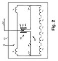
図1を引き続き参照し、図2をさらに参照して、磁石クライオスタット12に配置された超伝導磁石10をより詳細に説明する。磁石10のほとんどのコンポーネントに図2では符号が付されているが、図1では符号が付されていないことに留意されたい。超伝導磁石10は、複数の超伝導磁石コイルC1、C2、C3、C4、C5、C6、S1、S2を含む。複数の超伝導磁石コイルC1、C2、C3、C4、C5、C6、S1、S2は、磁石クライオスタット12の内部に配置され、電流が超伝導磁石コイルC1、C2、C3、C4、C5、C6、S1、S2に流れるとき静(B0)磁場を発生するように構成される。例示の超伝導磁石10は、6つの主コイルC1、C2、C3、C4、C5、C6と、2つのシールドコイルS1、S2とを含む。しかしながら、主コイルの数は6つ以外とすることができ、シールドコイルの数は2つ以外とすることができる。さらに、シールドコイルを完全に省略することが考えられる。超伝導磁石コイルC1、C2、C3、C4、C5、C6、S1、S2は、銅マトリクスに配分されたニオブチタン、ニオブ−スズなどのような任意の適切な超伝導材料の巻線を含む。高温超伝導材料の使用も考えられる。超伝導磁石10は、DC電源を接続して磁石電流をランプするために磁石クライオスタット12内のポートを介してアクセス可能な端子、磁石クライオスタット12の真空ジャケッティングなどのような概略の図2に示されていない他のコンポーネントを含む。磁石コイルC1、C2、C3、C4、C5、C6、S1、S2の位置、コイルごとの巻数、及び他の設計特性は、FOVにわたる高い空間均一性をもつイメージングFOV内の静B0磁場を生成するように設計される。
The
図1及び図2を引き続き参照すると、超伝導磁石10は、超伝導B0補償回路30をさらに含み、超伝導B0補償回路30は、磁石クライオスタット12の内部に配置され、超伝導磁石コイルによって発生されるB0磁場の時間的変動を低減するために超伝導磁石コイルC1、C2、C3、C4、C5、C6、S1、S2に結合される。図2の実施形態において、この結合は、主磁石コイルC1、C2、C3、C4、C5、C6とシールドコイルS1、S2との間を接続する端子との超伝導B0補償回路30の電気接続32、34によるものである。例示の超伝導B0補償回路30は、主磁石コイルC1、C2、C3、C4、C5、C6を横切る(又は等価的にシールドコイルS1、S2を横切る)超伝導短絡を含む。超伝導B0補償回路30は、望ましくない蓄積電流を除去するために回路30をリセットする目的で、又は磁石ランピング及びクエンチの間に回路30を開くために、超伝導スイッチ36をさらに含む。例えば、超伝導B0補償回路30のいくつかの好適な設計が、例えば、Reichert、米国特許第4,926,289号(「Actively shielded, superconducting magnet of an NMR tomography apparatus」、及びOverweg、米国特許第5,426,366号(「Magnetic resonance apparatus comprising a superconducting magnet」)に記載されている。しかしながら、超伝導B0補償回路30は、粗いB0補償(例えば10の程度の遮蔽率であるが、より高い又はより低い値が考えられる)を行うだけで十分である。結果として、設計制約が緩和される。例えば、そのような超伝導B0補償回路は、通常、設計基準遮蔽率を達成するために磁石コイルの内部で接続されなければならないが、図2の実施形態では、接続32、34は、超伝導磁石コイルC1、C2、C3、C4、C5、C6、S1、S2のうちのいずれかの外部の端子で行われ、それにより製造が単純になる。
With continued reference to FIGS. 1 and 2,
図1及び図2のB0補償は、イメージングFOVの(又はその近くの)外部B0磁場の通常の測定の代わりになる代用信号に基づいて動作する能動コンポーネントをさらに含む。この目的のために、電流センサ40が、磁石クライオスタット12の内部に配置され、超伝導B0補償回路30に流れる電流を測定するように接続される。超伝導B0補償回路30に流れる電流のこの測定は、能動B0補償に使用される代用信号である。電流センサ40は極低温電流センサである。その理由は、電流センサ40が、動作の間、磁石クライオスタット12の内部に配置され、それに応じて、例えば、超伝導磁石コイルの超伝導の臨界温度TCより低い極低温に維持されるからである。例示の電流センサ40には、超伝導センサコイル40を通過して超伝導B0補償回路30に流れる電流に応じてセンサコイル磁場を発生するための、超伝導B0補償回路30に電気的に接続された超伝導センサコイル42と、センサコイル磁場を測定するように構成された磁場センサ44とが含まれる。オプションの磁気シールド46は、超伝導センサコイル42及び磁場センサ44を取り囲む。例として、1つの実施形態では、磁場センサはホール効果センサとすることができるが、他の磁場センサが使用されてもよい。この例示の電流センサ設計では、センサコイル42は超伝導であるが、磁場センサ44は必ずしも超伝導コンポーネントではない(ただし磁場センサ44は例えばTCより低い極低温で動作可能である)ことに留意されたい。概略の図2にはそのように示されていないが、最大感度を得るために、磁場センサ44は超伝導センサコイル42の内部に配置されることが好ましく、超伝導センサコイル42は、例えば、ソレノイドコイルとすることができ、その結果、B0補償回路30に流れる(したがって、センサコイル42も通る)電流によって発生される磁場が、ソレノイドコイルのターン数だけ増幅される。オプションの磁気シールド46は、磁石クライオスタット12の内部のB0磁場及び/又は磁気的外乱が電流センサの動作に干渉するのを阻止する。いくつかの適切な実施形態では、磁気シールド46は、コイル/センサアセンブリ42、44を少なくとも部分的に取り囲むアルミニウム又は銅の円筒状遮蔽である。磁気干渉の低減は、追加として又は代替として、コンポーネント42、44を適切な向きにすることによっても得られる。例示の図2では、ソレノイドセンサコイル42は、B0磁場ベクトルを横切る向きの磁場ベクトルを生成するように配向されている。磁場センサ44が平面ホール効果センサである場合、それは、ソレノイドセンサコイル42によって発生された磁場を検出するが、B0磁場には非感受性であるように配向されている。
The B 0 compensation of FIGS. 1 and 2 further includes an active component that operates on a substitute signal that replaces the usual measurement of the external B 0 magnetic field (or near) of the imaging FOV. For this purpose, a
図1及び図2を引き続き参照し、図1に特に着目すると、極低温電流センサ40は、能動B0補償コンポーネント50によって受信される信号を出力する。例示の図1及び図2において、この信号は、電気接続52、例えば、磁場センサ44に接続され、クライオスタットフィードスルー(図示せず)を通って能動B0補償コンポーネント50に行くワイヤを介して伝えられる。(磁場センサ44はそれ自体超伝導コンポーネントでないので、このワイヤは超伝導である必要がなく、それによって構成が簡単になることに留意されたい。)代替実施形態(図示せず)では、極低温電流センサ40が、磁場センサ44の出力を能動B0補償コンポーネント50にワイヤレスで送信するワイヤレス送信器を含むことが考えられる。
Figure 1 and continuing reference to FIG. 2, in particular focusing on FIG 1, cryogenic
能動B0補償コンポーネント50は、任意の従来のB0補償機構を使用することができる。例えば、いくつかの実施形態では、能動B0補償コンポーネント50は、MRイメージングデバイス8により取得されたMRイメージングデータのMR周波数を調節することによって、超伝導B0補償回路30に流れる電流に基づいて能動B0磁場補償を行う。この手法は、B0補償コンポーネント50の出力をイメージングデータ取得ハードウェア22に供給する実線矢印によって図1に図式的に示されており、本明細書において図6を参照して後でより詳細に説明する。別の実施形態では、能動B0補償コンポーネント50は、MRイメージングデバイス8のMR周波数を調節することによって、例えば、B0補償コンポーネント50からRFトランシーバコンポーネント20まで延びる破線の出力矢印により図1に図式的に示されているようにRFトランシーバコンポーネント20を制御することによって、能動B0磁場補償を行う。また別の例示の手法では、能動B0補償コンポーネント50は、補償磁場を発生することによって、例えば、抵抗性コイル又は超伝導補償コイル(図示せず)に電気的にエネルギーを与えることによって、能動B0磁場補償を行う。例えば、Ham等、米国特許第6,731,113号(「Method of and device for the compensation of variations of the main magnetic field during magnetic resonance imaging」)を参照されたい。
Active B 0 compensation component 50 can use any conventional B 0 compensation mechanism. For example, in some embodiments, the active B 0 compensation component 50 is based on the current flowing through the superconducting B 0 compensation circuit 30 by adjusting the MR frequency of the MR imaging data acquired by the MR imaging device 8. Active B 0 magnetic field compensation is performed. This technique is graphically illustrated in FIG. 1 by a solid arrow supplying the output of the B 0 compensation component 50 to the imaging
図3を参照すると、代替実施形態では、磁石コイルへの電気接続32、34を有する図2の超伝導B0補償回路30が、超伝導B0補償回路60と取り替えられており、超伝導B0補償回路60は、B0補償回路60の補償回路コイルCC1、CC2と超伝導主磁石コイルC1、C2、C3、C4、C5、C6との間の誘導結合によって超伝導磁石コイルに結合されている。図3の超伝導B0補償回路60は、回路60をリセットする目的で前に説明した超伝導スイッチ36をさらに含み、(図の事例では)オプションの磁気シールド46とともに、超伝導センサコイル42と、センサコイル磁場を測定するように構成された磁場センサ44とを含む前に説明した極低温電流センサ40を接続している。図2の実施形態と同様に、図3の超伝導B0補償回路60は、粗いB0補償(例えば、10の程度の遮蔽率)を行うだけで十分である。結果として、設計制約が緩和される。例えば、より少ない数の補償回路コイルCC1、CC2、例えば、例示の図3では2つの補償回路コイルCC1、CC2のみを結合のために使用することができ、それにより製造が単純になる。
Referring to FIG. 3, in the alternative embodiment, the superconducting B 0 compensating circuit 30 of FIG. 2 having
図4を参照すると、別の代替実施形態では、超伝導B0補償回路70は、図3の回路60と類似しているが、シールドコイルS1、S2に結合されている。具体的には、図4の事例では、補償回路コイルCC1はシールドコイルS1に結合され、補償回路コイルCC2はシールドコイルS2に結合される。図4の超伝導B0補償回路70は、回路70をリセットする目的で、前に説明した超伝導スイッチ36をさらに含み、(事例では)オプションの磁気シールド46とともに、超伝導センサコイル42と、センサコイル磁場を測定するように構成された磁場センサ44とを含む前に説明した極低温電流センサ40を接続している。この場合も、超伝導B0補償回路70は、粗いB0補償(例えば、10の程度の遮蔽率)を行うだけで十分である。結果として、設計制約が緩和される。例えば、より少ない数の補償回路コイルCC1、CC2を使用することができる。
Referring to FIG. 4, in another alternative embodiment, the superconducting B 0 compensation circuit 70 is similar to the
図4の実施形態において、B0補償回路70の補償回路コイルCC1、CC2は、ボア14の軸に対してより大きい半径のところに(すなわち、磁石アイソセンタから遠く離れて)置かれ、シールドコイルS1、S2の近くに置かれる。これにはいくつかの利点がある。この構成の補償回路コイルCC1、CC2は、大きいピックアップ区域を有し、イメージングFOVにおいて比較的小さい補正磁場を発生し、イメージングFOVにおいて比較的均一な磁場を発生することができる。補償コイルCC1、CC2が磁石アイソセンタから遠く離れているのでB0補償回路70の構成は受動補償が小さいことを当業者は予期するが、これは、図4の構成において、補償コイルCC1、CC2の主磁石コイルC1、C2、C3、C4、C5、C6との若干の結合も存在するので必ずしも正しくはない。B0補償回路70の電流変化は、磁石の主磁石コイルC1、C2、C3、C4、C5、C6の電流変化を引き起こし、それは、さらに、受動B0補償コンポーネントに寄与する補償磁場を与える。
In the embodiment of FIG. 4, the compensation circuit coils CC 1 and CC 2 of the B 0 compensation circuit 70 are placed at a larger radius with respect to the axis of the bore 14 (that is, far away from the magnet isocenter) and shielded. placed near the
次に図5を参照すると、B0補償回路60又はB0補償回路70に直列に接続された余分な磁場コイルの電気回路図が示される。図5を参照して、これらの実施形態で磁場増幅を得る方法を説明する。補償コイルCC1、CC2の設計は、外乱磁場Bdistに対して磁場センサ44のところで最大磁場増幅を与えるように(言い換えれば、磁場センサ44のところに磁場を最適に集中させるように)最適化される。外部源からの外乱磁場Bdistは、B0補償回路60、70の大径補償コイルCC1、CC2によってピックアップされる。補償回路のすべての補償コイルCC1、CC2は、電気的に直列に接続され、外乱磁場Bdistとの結合では単一のピックアップコイルとして効果的に動作する。この単一の効果的なピックアップコイルは、図5においてインダクタンスLpとして表わされている。すべての補償コイルCC1、CC2の総合計面積はApである。さらに、磁場センサ44を取り囲む(磁場センサ44に少なくとも結合される)超伝導センサコイル42があり、このセンサコイル42のインダクタンスはインダクタンスLsで表される。センサコイル42は、nsターン、総合計面積As、及び磁場定数ksを有する。
Next, referring to FIG. 5, an electric circuit diagram of an extra magnetic field coil connected in series with the B 0 compensation circuit 60 or the B 0 compensation circuit 70 is shown. A method of obtaining magnetic field amplification in these embodiments will be described with reference to FIG. The design of the compensating coils CC 1 and CC 2 is optimal so that the disturbance magnetic field B dust is given maximum magnetic field amplification at the magnetic field sensor 44 (in other words, the magnetic field is optimally concentrated at the magnetic field sensor 44). Be transformed. The disturbance magnetic field B dust from the external source is picked up by the large diameter compensation coils CC 1 and CC 2 of the B 0 compensation circuits 60 and 70. All the compensating coils CC 1 and CC 2 of the compensating circuit are electrically connected in series and effectively operate as a single pickup coil in combination with the disturbance magnetic field B dust . This single effective pickup coil is represented in FIG. 5 as the inductance L p . Total total area of all the
外部磁場(又は実際にはそのz成分)が量Bdist(これは外乱磁場Bdistである)だけ変化する場合、これは、B0補償回路60又はB0補償回路70に磁束Bdist・Apを発生する。これは、図5にIで示されたB0補償回路の電流変化を与え、これは、磁場センサ44に磁場変化Bs=I・ksを与える。誘導電流Iは、超伝導回路の全磁束が一定のままであるということから計算される。そこで、
Bs=I・ks
及び
Bdist・Ap+I・(Lp+Ls)=0
であり、その結果、
Bs/Bdist=−ks・Ap/(Lp+Ls)
である。例示の設計プロセスは以下の通りである。補償コイルCC1、CC2を容易に巻くことができる場所、及び実際に使用されるターン数などの実際的な考慮から得られる所与の補償コイルCC1、CC2から開始する。これらの考慮は、補償コイルCC1、CC2、より詳しくはAp及びLpの値を規定する。次いで、比Bs/Bdistが最大になるように、Ls及びksの値が最適化される。Lsを与えるセンサコイル42は、Lpに比べて多いターン数をもつ小さいコイルであるべきであることが分かる。適切な手法で、インダクタンスLsは、実際的な考慮事項によって選ばれる。適切な目標はLs≒Lpであり、その理由は、これが最適な磁束トランスをもたらすからである。次いで、磁場センサ44のまわりにぴったり適合するコイルLsの最小直径を決定する。最後に、センサコイル42のターン数nsがLs≒Lpまで増加される。
If the external magnetic field (or its z component) changes by the amount B dust (which is the disturbance magnetic field B dust ), then this is the magnetic flux B dust A to the B 0 compensation circuit 60 or B 0 compensation circuit 70. Generate p . This gives the current change of the B 0 compensation circuit shown by I in FIG. 5, which gives the
B s = I · k s
And B dust · A p + I · (L p + L s ) = 0
And as a result,
B s / B dist = -k s · A p / (L p + L s)
Is. The exemplary design process is as follows. Start with the given compensating coils CC 1 and CC 2 obtained from practical considerations such as where the compensating coils CC 1 and CC 2 can be easily wound and the number of turns actually used. These considerations specify the values of the compensation coils CC 1 , CC 2 , and more specifically Ap and L p . The values of L s and k s are then optimized so that the ratio B s / B dust is maximized. It can be seen that the
一例として、Lpを規定する補償コイルCC1、CC2が、各々1.50メートルの直径の2ターンを有し、一方、Lsを規定するセンサコイル42が、6mm直径の小さい管に巻かれた68ターンを有する場合、以下の近似値が見いだされる。この場合、Ap=1.8m2、Lp=18μH、Ls=18μH、及びks=0.01T/Aである。すると、これは、Bs/Bdist=500の磁場増幅を与える。これは単に説明のための例であり、より一般的には、この値はコイルの実際の形状に基づいて選択される。加えて、磁石の主コイルとの結合がオプションとして考慮に入れられるが、これは、例示を簡単にするために上記の例では無視されている。非常に重要な磁場増幅が上記の手法によって得られることが分かる。この増幅により、より低コストの磁場センサを使用することができ、及び/又は所与の磁場センサに対してより良好な感度を得ることができる。
As an example, the compensating coils CC 1 and CC 2 defining L p each have two turns with a diameter of 1.50 meters, while the
磁場センサ44は、磁石10の主B0磁場の振幅及び空間傾斜が比較的低い磁石クライオスタット12内の位置に置かれることが好ましい。さらに、やはり、磁場センサ44は、B0磁場に対して低い感度又はゼロの感度を有するように、主B0磁場を横切る向きにされるべきである。これらの手法は、代替として又は組合せて、振動誘起磁場誤差の潜在的な影響を低減し、範囲が限られた磁場センサ、例えば、従来のホールプローブ、巨大磁気抵抗(GMR)センサ、又は磁束ゲート磁力計の使用を容易にする。
The
代替として、磁場センサは、磁気共鳴(MR)ベースプローブとすることができる。その理由は、MRデバイス8が、そのようなMRプローブを駆動し読み取るための基盤を有するからである。この変形実施形態では、MRプローブの方位は主B0磁場と一直線になっていなければならない。磁場が適度に均一である磁石内の位置が選ばれるべきであり、その位置が高磁場区域である場合、それは問題とはならない。このプローブでは、MRプローブの感度が高いので、増幅Bs/Bdistはあまり重要でなくなる。 Alternatively, the magnetic field sensor can be a magnetic resonance (MR) based probe. The reason is that the MR device 8 has a basis for driving and reading such an MR probe. In this modified embodiment, the orientation of the MR probe must be in line with the main B 0 magnetic field. A position within the magnet where the magnetic field is reasonably uniform should be chosen, and if that position is in the high magnetic field area, it does not matter. With this probe, the amplification B s / B dust is less important due to the high sensitivity of the MR probe.
次に図6を参照して、MRイメージングデバイス8により取得されたMRイメージングデータのMR周波数を調節することによって、超伝導B0補償回路30に(又は回路60に、又は回路70に)流れる電流に基づいて能動B0磁場補償を行う能動B0補償コンポーネント50の例示の実施形態を説明する。この手法では、伝達関数を使用して、磁場感知の利得及び周波数依存特性を扱う。磁場センサ44は、磁場に対して低域通過フィルタとして振る舞う金属筐体であるクライオスタット12の内部に置かれる。したがって、磁場センサ44の感度は、外部外乱の周波数が増加するにつれて低下する。これは、例えば超伝導磁石10の開発段階の間に一度測定又は計算された伝達関数を使用して補正される。測定は以下のように行われる。それは、磁石に均一の外部磁場を発生させるソースコイルを必要とする。次に、周波数掃引によりこのソースコイルを駆動するとき、磁場は、磁場センサ44、並びに磁石10のアイソセンタに置かれた別の較正プローブ(この他の較正プローブは室温で動作している)を用いて測定されるべきである。H(ω)が極低温磁場センサ44を用いて測定された応答であり、G(ω)が磁石アイソセンタで室温較正プローブを用いて測定された磁場応答であるとする。すると、G(ω)は、受動B0補償が受動B0補償回路30(又は回路60、又は回路70)によって行われた後に得られる正味磁場であり、B0磁場変動の残りは能動的に補償されるべきである。H(ω)はその残りの磁場に対応するセンサ信号である。そのため、G(ω)/H(ω)を、能動B0補償のための伝達関数として使用することができる(これは、極低温磁場センサ44によって測定された信号に対して利得並びに周波数補正を設定する)。次いで、補正された信号がMRイメージングデバイス8によって使用されて、B0の残りのずれが補償される。これは、前に説明したようないくつかのやり方で、例えば、MRデータを補正することによって、又はRF周波数を調節することによって、又は補償磁場を印加することによって行われる。図6の例示の実施形態では、信号は補正されたMR周波数f0に変換され、それは周波数補正としてMRイメージングデータ取得ハードウェア22に供給される。この能動B0補償手法は、回転磁気関係42.58MHz/TのためにB0又はf0のシフトが等価であるという観察に基づく。シフトされたMR周波数f0が、ソフトウェアで、図6に示すように、生MRデータを補正することによってもたらされる。代替として、図1に示した能動B0補償コンポーネント50からの破線の出力矢印で示すように、この補正されたMR周波数f0は、RFトランシーバハードウェア20の周波数をシフトすることによってハードウェアで適用されてもよい。
Next, referring to FIG. 6, the current flowing in the superconducting B0 compensation circuit 30 (or in the
一般に、能動B0補償コンポーネント50は、伝達関数G(ω)/H(ω)を実現するデジタル信号処理(DSP)としての上記の信号処理と、補正されたMR周波数f0への変換とを実現するようにプログラムされた電子プロセッサ(例えば、コンピュータ、マイクロコントローラなど)を含む。ソフトウェアベース補正では、これは、例えば画像再構成24を実施するMRイメージングデータ処理ソフトウェアと一体化されてもよい。RFトランシーバハードウェア20が制御される実施形態では、この手法は、補正されたf0をこのハードウェア20のデジタル又はアナログ周波数セットポイント制御部に供給する。代替実施形態では、アナログ信号処理回路を使用して、例えばオペアンプ(opアンプ)ベース回路を使用して、オプションとして、デジタル補正f0出力が必要とされる場合アナログ−デジタル(A/D)変換器とともに、信号処理を実施することが考えられる。
In general, the active B 0 compensation component 50 performs the above signal processing as digital signal processing (DSP) that realizes the transfer function G (ω) / H (ω) and conversion to the corrected MR frequency f 0 . Includes electronic processors programmed to implement (eg, computers, microcontrollers, etc.). In software-based correction, this may be integrated with MR imaging data processing software that performs, for example,
例示のB0補償の実施形態は、外部外乱磁場の均一な部分を補償し、それは通常十分である。他の考えられる実施形態では、B0補償は、外部外乱磁場のx、y、及び/又はz傾斜に同様に適用される。この手法は、外乱磁場の均一部分の補正と類似しているが、ピックアップコイルの形状は、x、y、及びz傾斜コイルの形状に類似するように選ばれる。この拡張により、磁石の近くにある外乱源に対する補償が改善される。 An exemplary B0 compensation embodiment compensates for a uniform portion of the external disturbance magnetic field, which is usually sufficient. In embodiments where other possible, B 0 compensation is similarly applied to the external disturbance magnetic field of x, y, and / or z-gradient. This method is similar to the correction of the uniform portion of the disturbance magnetic field, but the shape of the pickup coil is chosen to be similar to the shape of the x, y, and z tilt coils. This extension improves compensation for disturbance sources near the magnet.
好ましい実施形態を参照して本発明を説明した。先の詳細な説明を読み理解する際に、変更及び改変を他者が思いつくことがある。本発明は、すべてのそのような変更及び改変が添付の特許請求の範囲又はその均等物の範囲内にある限り、すべてのそのような変更及び改変を含むと解釈されることが意図されている。 The present invention has been described with reference to preferred embodiments. Others may come up with changes and modifications as they read and understand the detailed explanation above. The present invention is intended to be construed as including all such modifications and modifications, as long as all such modifications and modifications are within the scope of the appended claims or equivalents thereof. ..
Claims (19)
前記磁石クライオスタットの内部に配置され、電流が流れるとき静磁場(B0)を発生する超伝導磁石コイルと、
前記磁石クライオスタットの内部に配置され、前記超伝導磁石コイルによって発生される前記静磁場の時間的変動を低減するために前記超伝導磁石コイルに結合された超伝導B0補償回路と、
前記磁石クライオスタットの内部に配置され、前記超伝導B0補償回路に流れる電流を測定するように接続された電流センサと、
前記超伝導B0補償回路に流れる電流の測定値を受け取るために前記電流センサに動作可能に接続され、前記超伝導B0補償回路に流れる電流に基づいて能動静磁場補償を行う能動B0補償コンポーネントと
を含む、超伝導磁石。 With the magnet cryostat,
A superconducting magnet coil that is placed inside the magnet cryostat and generates a static magnetic field (B 0 ) when an electric current flows.
Wherein disposed within the magnet cryostat, the superconducting B 0 compensation circuit coupled to said superconducting magnet coils in order to reduce the time variation of the said static magnetic field generated by superconducting magnet coils,
A current sensor located inside the magnet cryostat and connected to measure the current flowing through the superconducting B0 compensation circuit.
Said operatively connected to said current sensor for receiving a measurement of the current flowing through the superconducting B 0 compensation circuit, the active B 0 compensate that actively static magnetic field compensation based on the current flowing through the superconducting B 0 compensation circuit Superconducting magnets, including components.
超伝導センサコイルを通過して前記超伝導B0補償回路に流れる電流に応じて、センサコイル磁場を発生するための、前記超伝導B0補償回路に電気的に接続された超伝導センサコイルと、
前記センサコイル磁場を測定する磁場センサと
を含む、請求項1に記載の超伝導磁石。 The current sensor
Depending on the current flowing through the superconducting B 0 compensation circuit through a superconducting sensor coils, for generating a sensor coil magnetic field, a superconducting sensor coils the electrically connected to the superconducting B 0 compensation circuit ,
The superconducting magnet according to claim 1, further comprising a magnetic field sensor for measuring the sensor coil magnetic field.
前記磁場センサが、前記センサコイル磁場を感知し、前記センサコイル磁場を横切る向きの前記静磁場を感知しないように配向されている、請求項5に記載の超伝導磁石。 The superconducting sensor coil is oriented at the current sensor to generate the sensor coil magnetic field in a direction across the static magnetic field.
The superconducting magnet according to claim 5, wherein the magnetic field sensor is oriented so as to sense the sensor coil magnetic field and not the static magnetic field in a direction crossing the sensor coil magnetic field.
前記超伝導B0補償回路が、前記補償回路コイルと、(1)前記主コイル及び(2)前記シールドコイルの一方との間の誘導結合によって前記超伝導磁石コイルに結合される、請求項10に記載の超伝導磁石。 The superconducting magnet coil includes a main coil and a shield coil.
10. The superconducting B0 compensation circuit is coupled to the superconducting magnet coil by an inductive coupling between the compensation circuit coil and one of (1) the main coil and (2) the shield coil. The superconducting magnet described in.
磁石クライオスタットを使用して、超伝導磁石コイルと、前記超伝導磁石コイルに結合された超伝導B0補償回路とを冷却するステップと、
前記超伝導磁石コイルに電気的にエネルギーを与えて静磁場(B0)を発生するステップと、
前記超伝導B0補償回路を使用して前記静磁場の時間的変動を低減するステップと、
前記磁石クライオスタットの内部に配置された電流センサを使用して、前記超伝導B0補償回路に流れる電流を測定するステップと、
前記超伝導B0補償回路に流れる、測定された電流に基づいて能動静磁場補償を実行するステップと
を有する、方法。 A method of operating a superconducting magnet, wherein the method is
And cooling using a magnet cryostat, the superconducting magnet coil, said superconducting B 0 compensation circuit coupled to the superconducting magnet coil,
A step of electrically applying energy to the superconducting magnet coil to generate a static magnetic field (B 0 ), and
A step of reducing the temporal fluctuation of the static magnetic field by using the superconducting B0 compensation circuit, and
A step of measuring the current flowing through the superconducting B0 compensation circuit using a current sensor arranged inside the magnet cryostat, and a step of measuring the current flowing through the superconducting B0 compensation circuit.
A method comprising the step of performing active static magnetic field compensation based on a measured current flowing through the superconducting B0 compensation circuit.
前記超伝導B0補償回路に流れる前記測定された電流に基づいて、前記静磁場に配置された対象者から取得された磁気共鳴イメージングデータの周波数を調節するステップを有する、請求項12に記載の方法。 The step of performing active static magnetic field compensation is
12. The twelfth aspect of claim 12 , wherein the step comprises adjusting the frequency of magnetic resonance imaging data acquired from a subject placed in the static magnetic field based on the measured current flowing through the superconducting B0 compensation circuit. Method.
前記超伝導B0補償回路に流れる前記測定された電流に基づいて、前記静磁場に配置された対象者から磁気共鳴イメージングデータを取得する磁気共鳴イメージングデバイスの磁気共鳴周波数を調節するステップを有する、請求項12に記載の方法。 The step to be performed is
A step of adjusting the magnetic resonance frequency of a magnetic resonance imaging device that acquires magnetic resonance imaging data from a subject placed in the static magnetic field based on the measured current flowing through the superconducting B0 compensation circuit. The method according to claim 12 .
前記超伝導B0補償回路に流れる前記測定された電流に基づいて補償磁場を発生するステップを有する、請求項12に記載の方法。 The step to be performed is
12. The method of claim 12 , comprising the step of generating a compensating magnetic field based on the measured current flowing through the superconducting B0 compensating circuit.
前記超伝導B0補償回路に流れる電流の測定値を受け取るために前記電流センサに動作可能に接続され、前記超伝導B0補償回路に流れる前記電流に基づいて能動静磁場補償を行う能動B0補償コンポーネントと
を含む、磁気共鳴イメージングデバイス。 A magnet cryostat, the superconducting magnet coil disposed inside the magnet cryostat, and the disposed inside the magnet cryostat, the superconducting superconducting B 0 compensation circuit coupled to the magnet coil, the interior of the magnet cryostat A superconducting magnet, including a current sensor arranged in, and connected to measure the current flowing through the superconducting B0 compensating circuit.
Wherein said operatively connected to the current sensor to receive a measurement of the current flowing through the superconducting B 0 compensation circuit, an active B 0 that actively static magnetic field compensation, based on the current flowing through the superconducting B 0 compensation circuit Magnetic resonance imaging device, including with compensation components.
前記超伝導B0補償回路に電気的に接続された超伝導センサコイルと、
前記超伝導センサコイルによって発生された磁場を測定する磁場センサと
を含む、請求項16に記載の磁気共鳴イメージングデバイス。
The current sensor
A superconducting sensor coil electrically connected to the superconducting B0 compensation circuit,
The magnetic resonance imaging device according to claim 16 , further comprising a magnetic field sensor that measures a magnetic field generated by the superconducting sensor coil.
Applications Claiming Priority (3)
| Application Number | Priority Date | Filing Date | Title |
|---|---|---|---|
| US201662346672P | 2016-06-07 | 2016-06-07 | |
| US62/346,672 | 2016-06-07 | ||
| PCT/EP2017/063597 WO2017211756A1 (en) | 2016-06-07 | 2017-06-05 | Cryogenic field sensing for compensating magnetic field variations in magnetic resonance imaging magnets |
Publications (3)
| Publication Number | Publication Date |
|---|---|
| JP2019524177A JP2019524177A (en) | 2019-09-05 |
| JP2019524177A5 JP2019524177A5 (en) | 2020-09-10 |
| JP6828058B2 true JP6828058B2 (en) | 2021-02-10 |
Family
ID=59009695
Family Applications (1)
| Application Number | Title | Priority Date | Filing Date |
|---|---|---|---|
| JP2018563821A Expired - Fee Related JP6828058B2 (en) | 2016-06-07 | 2017-06-05 | Magnetic Resonance Imaging Cryogenic magnetic field sensing to compensate for magnetic field fluctuations in magnets |
Country Status (5)
| Country | Link |
|---|---|
| US (1) | US10761163B2 (en) |
| EP (1) | EP3465245A1 (en) |
| JP (1) | JP6828058B2 (en) |
| CN (1) | CN109313245B (en) |
| WO (1) | WO2017211756A1 (en) |
Families Citing this family (6)
| Publication number | Priority date | Publication date | Assignee | Title |
|---|---|---|---|---|
| WO2017064539A1 (en) * | 2015-10-16 | 2017-04-20 | Synaptive Medical (Barbados) Inc. | Magnetic resonance imaging system capable of rapid field ramping |
| WO2020254158A1 (en) * | 2019-06-20 | 2020-12-24 | Koninklijke Philips N.V. | Quench protection for high temperature superconducting (hts) leads |
| US12039403B2 (en) * | 2020-12-22 | 2024-07-16 | International Business Machines Corporation | Semi-active magnetic shielding for qubit unit components of quantum computing apparatuses |
| EP4053860B1 (en) * | 2021-03-05 | 2023-06-21 | Bruker Switzerland AG | A method for charging a superconductor bulk magnet by field-cooling, with at least one non-homogeneous magnetic field component of the applied charger magnetic field |
| CN113534028B (en) * | 2021-06-30 | 2023-03-10 | 中南大学湘雅二医院 | A skin-specific surface phased array receiving coil |
| JP2025027386A (en) * | 2023-08-14 | 2025-02-27 | キヤノンメディカルシステムズ株式会社 | Magnetic Resonance Imaging System |
Family Cites Families (26)
| Publication number | Priority date | Publication date | Assignee | Title |
|---|---|---|---|---|
| EP0299325B1 (en) | 1987-07-17 | 1991-12-18 | Siemens Aktiengesellschaft | Actively shielded supraconducting magnet of a nuclear spin tomographic apparatus |
| US5214383A (en) | 1990-10-29 | 1993-05-25 | Resonex, Inc. | MRI apparatus with external magnetic field compensation |
| US5426366A (en) * | 1992-12-11 | 1995-06-20 | U.S. Philips Corporation | Magnetic resonance apparatus comprising a superconducting magnet |
| DE19510142A1 (en) | 1995-03-21 | 1996-09-26 | Siemens Ag | Magnetic resonance device with stray magnetic field compensation |
| DE19536390A1 (en) | 1995-09-29 | 1997-04-03 | Siemens Ag | Fundamental field measurement appts. for controlling fundamental field of NMR tomography magnet |
| JP3753505B2 (en) * | 1997-07-07 | 2006-03-08 | ジーイー横河メディカルシステム株式会社 | Disturbance magnetic field compensation method and magnetic resonance imaging apparatus |
| JPH11164820A (en) * | 1997-12-05 | 1999-06-22 | Hitachi Medical Corp | Superconducting magnet |
| WO2000054069A1 (en) | 1999-03-10 | 2000-09-14 | Koninklijke Philips Electronics N.V. | Method of and device for the compensation of variations of the main magnetic field during magnetic resonance imaging |
| US6396268B1 (en) | 2000-10-02 | 2002-05-28 | Ge Medical Systems Global Technology Company, Llc | Magnetic resonance imaging device having magnetic field disturbance compensation |
| JP3884243B2 (en) | 2001-06-21 | 2007-02-21 | ジーイー・メディカル・システムズ・グローバル・テクノロジー・カンパニー・エルエルシー | External magnetic field measurement method, static magnetic field correction method, external magnetic field measurement apparatus, and MRI apparatus |
| JP4193382B2 (en) * | 2001-07-19 | 2008-12-10 | 株式会社日立製作所 | Magnetic field measuring device |
| US6960914B2 (en) * | 2003-06-27 | 2005-11-01 | Ge Medical Systems Global Technology Company, Llc | Methods and apparatus for imaging systems |
| EP1938083A2 (en) * | 2005-10-12 | 2008-07-02 | Koninklijke Philips Electronics N.V. | Magnetic sensor device with field compensation |
| JP2008020266A (en) * | 2006-07-11 | 2008-01-31 | National Institute For Materials Science | Superconducting magnet device |
| DE102006035949B4 (en) | 2006-07-31 | 2009-11-26 | Bruker Biospin Ag | Apparatus and method for compensating magnetic field disturbances in high field homogeneity magnetic fields |
| CN100495597C (en) * | 2006-09-30 | 2009-06-03 | 中国科学院电工研究所 | Conduction Cooled Superconducting Magnet System for Gyrotron |
| GB2457729B (en) * | 2008-02-25 | 2010-03-10 | Siemens Magnet Technology Ltd | Superconducting magnet current adjustment by flux pumping |
| CN101422365B (en) * | 2008-12-16 | 2010-12-01 | 中国科学院物理研究所 | Adjustment device and adjustment method for balanced pulse external magnetic field in high temperature SQUID application |
| JP5222324B2 (en) * | 2010-07-14 | 2013-06-26 | 株式会社日立製作所 | Superconducting coil, superconducting magnet and operation method thereof |
| US8604793B2 (en) * | 2010-10-21 | 2013-12-10 | General Electric Company | Superconducting magnet having cold iron shimming capability |
| US9279871B2 (en) | 2011-12-20 | 2016-03-08 | General Electric Company | System and apparatus for compensating for magnetic field distortion in an MRI system |
| WO2014025265A1 (en) * | 2012-08-07 | 2014-02-13 | Hts-110 Limited | Improved magnetic field control |
| EP2954343A1 (en) * | 2013-02-06 | 2015-12-16 | Koninklijke Philips N.V. | Active compensation for field distorting components in a magnetic resonance imaging system with a gantry |
| CN103616650B (en) * | 2013-11-25 | 2017-04-19 | 中国科学院上海微系统与信息技术研究所 | Superconducting magnetic compensation device and method based on predistortion |
| US9810755B2 (en) * | 2013-12-16 | 2017-11-07 | General Electric Company | System and method for energizing a superconducting magnet |
| CN104224179A (en) * | 2014-09-10 | 2014-12-24 | 中国科学院电工研究所 | Magnetic field stabilizing method and device for magnetic resonance imaging system |
-
2017
- 2017-06-05 JP JP2018563821A patent/JP6828058B2/en not_active Expired - Fee Related
- 2017-06-05 US US16/305,946 patent/US10761163B2/en active Active
- 2017-06-05 EP EP17727883.5A patent/EP3465245A1/en not_active Withdrawn
- 2017-06-05 WO PCT/EP2017/063597 patent/WO2017211756A1/en not_active Ceased
- 2017-06-05 CN CN201780035546.2A patent/CN109313245B/en active Active
Also Published As
| Publication number | Publication date |
|---|---|
| CN109313245B (en) | 2021-05-14 |
| EP3465245A1 (en) | 2019-04-10 |
| CN109313245A (en) | 2019-02-05 |
| US20190154777A1 (en) | 2019-05-23 |
| WO2017211756A1 (en) | 2017-12-14 |
| US10761163B2 (en) | 2020-09-01 |
| JP2019524177A (en) | 2019-09-05 |
Similar Documents
| Publication | Publication Date | Title |
|---|---|---|
| JP6828058B2 (en) | Magnetic Resonance Imaging Cryogenic magnetic field sensing to compensate for magnetic field fluctuations in magnets | |
| US7414401B1 (en) | System and method for shielded dynamic shimming in an MRI scanner | |
| US5227728A (en) | Gradient driver control in magnetic resonance imaging | |
| US9279871B2 (en) | System and apparatus for compensating for magnetic field distortion in an MRI system | |
| US8314615B2 (en) | Apparatus and method to improve magnet stability in an MRI system | |
| JP5512003B2 (en) | Gradient coil system with correction winding and manufacturing method thereof | |
| JP2010525892A (en) | Low magnetic field SQUID-MRI apparatus, component and method | |
| US9810755B2 (en) | System and method for energizing a superconducting magnet | |
| US9274188B2 (en) | System and apparatus for compensating for magnetic field distortion in an MRI system | |
| CN103389480A (en) | MR antenna with compensation for variable distance to shield | |
| US6825667B1 (en) | Magnetic resonance imaging apparatus and method for maintaining high uniformity of magnetic field in magnetic resonance imaging apparatus | |
| US5631561A (en) | Arrangement for measuring and controlling the basic field of an NMR tomography apparatus | |
| US6960914B2 (en) | Methods and apparatus for imaging systems | |
| US9989617B2 (en) | B1 field-based regulation within a sequence for NMR | |
| US20040021465A1 (en) | Non-coupling magnetic sheilding coil | |
| US7224167B2 (en) | Magnetic field generating apparatus and method for magnetic resonance imaging | |
| US20090206839A1 (en) | System, method and apparatus for compensating for drift in a main magnetic field in an mri system | |
| US9182465B2 (en) | MRT gradient system with integrated main magnetic field generation | |
| GB2343251A (en) | MRI gradient field probe | |
| Felder et al. | MRI Instrumentation | |
| US20050146332A1 (en) | Method and apparatus for magnetic resonance imaging | |
| JP4067546B2 (en) | Magnetic resonance imaging apparatus and static magnetic field uniformity maintaining method | |
| Kelley | Hardware Considerations in Ultra High Field MRI: An Overview of System Integration | |
| JP7049123B2 (en) | Magnetic resonance imaging device | |
| Klein | MRI System |
Legal Events
| Date | Code | Title | Description |
|---|---|---|---|
| A521 | Request for written amendment filed |
Free format text: JAPANESE INTERMEDIATE CODE: A523 Effective date: 20200604 |
|
| A621 | Written request for application examination |
Free format text: JAPANESE INTERMEDIATE CODE: A621 Effective date: 20200604 |
|
| A521 | Request for written amendment filed |
Free format text: JAPANESE INTERMEDIATE CODE: A523 Effective date: 20200731 |
|
| A871 | Explanation of circumstances concerning accelerated examination |
Free format text: JAPANESE INTERMEDIATE CODE: A871 Effective date: 20200731 |
|
| A975 | Report on accelerated examination |
Free format text: JAPANESE INTERMEDIATE CODE: A971005 Effective date: 20200819 |
|
| A131 | Notification of reasons for refusal |
Free format text: JAPANESE INTERMEDIATE CODE: A131 Effective date: 20200901 |
|
| A521 | Request for written amendment filed |
Free format text: JAPANESE INTERMEDIATE CODE: A523 Effective date: 20201130 |
|
| TRDD | Decision of grant or rejection written | ||
| A01 | Written decision to grant a patent or to grant a registration (utility model) |
Free format text: JAPANESE INTERMEDIATE CODE: A01 Effective date: 20201222 |
|
| A61 | First payment of annual fees (during grant procedure) |
Free format text: JAPANESE INTERMEDIATE CODE: A61 Effective date: 20210120 |
|
| R150 | Certificate of patent or registration of utility model |
Ref document number: 6828058 Country of ref document: JP Free format text: JAPANESE INTERMEDIATE CODE: R150 |
|
| LAPS | Cancellation because of no payment of annual fees |