JP6804228B2 - Magnetic resonance imaging device - Google Patents
Magnetic resonance imaging device Download PDFInfo
- Publication number
- JP6804228B2 JP6804228B2 JP2016151458A JP2016151458A JP6804228B2 JP 6804228 B2 JP6804228 B2 JP 6804228B2 JP 2016151458 A JP2016151458 A JP 2016151458A JP 2016151458 A JP2016151458 A JP 2016151458A JP 6804228 B2 JP6804228 B2 JP 6804228B2
- Authority
- JP
- Japan
- Prior art keywords
- data
- circuit
- pulse
- resonance imaging
- data string
- Prior art date
- Legal status (The legal status is an assumption and is not a legal conclusion. Google has not performed a legal analysis and makes no representation as to the accuracy of the status listed.)
- Active
Links
Images


Classifications
-
- G—PHYSICS
- G01—MEASURING; TESTING
- G01R—MEASURING ELECTRIC VARIABLES; MEASURING MAGNETIC VARIABLES
- G01R33/00—Arrangements or instruments for measuring magnetic variables
- G01R33/20—Arrangements or instruments for measuring magnetic variables involving magnetic resonance
- G01R33/44—Arrangements or instruments for measuring magnetic variables involving magnetic resonance using nuclear magnetic resonance [NMR]
- G01R33/48—NMR imaging systems
- G01R33/54—Signal processing systems, e.g. using pulse sequences ; Generation or control of pulse sequences; Operator console
- G01R33/56—Image enhancement or correction, e.g. subtraction or averaging techniques, e.g. improvement of signal-to-noise ratio and resolution
- G01R33/5608—Data processing and visualization specially adapted for MR, e.g. for feature analysis and pattern recognition on the basis of measured MR data, segmentation of measured MR data, edge contour detection on the basis of measured MR data, for enhancing measured MR data in terms of signal-to-noise ratio by means of noise filtering or apodization, for enhancing measured MR data in terms of resolution by means for deblurring, windowing, zero filling, or generation of gray-scaled images, colour-coded images or images displaying vectors instead of pixels
Landscapes
- Physics & Mathematics (AREA)
- Engineering & Computer Science (AREA)
- Signal Processing (AREA)
- High Energy & Nuclear Physics (AREA)
- Condensed Matter Physics & Semiconductors (AREA)
- General Physics & Mathematics (AREA)
- Artificial Intelligence (AREA)
- Computer Vision & Pattern Recognition (AREA)
- Health & Medical Sciences (AREA)
- General Health & Medical Sciences (AREA)
- Nuclear Medicine, Radiotherapy & Molecular Imaging (AREA)
- Radiology & Medical Imaging (AREA)
- Magnetic Resonance Imaging Apparatus (AREA)
Description
本発明の実施形態は、磁気共鳴イメージング装置に関する。 Embodiments of the present invention relate to a magnetic resonance imaging apparatus.
磁気共鳴イメージング装置において、RF(Radio Frequency)パルスを生成するために、例えばDDS(Direct Digital Synthesizer)等の送信技術が用いられることがある。かかる場合、まず出力予定のRFパルスのエンベロープに関するデジタルデータが、RFパルスのベースバンドの周波数帯域により定められる一定の時間間隔(例えば1μ秒間隔等)で生成され、生成された一定の時間間隔のデジタルデータを基に、RFパルスが生成される。 In a magnetic resonance imaging apparatus, a transmission technique such as a DDS (Direct Digital Synthesizer) may be used to generate an RF (Radio Frequency) pulse. In such a case, first, digital data regarding the envelope of the RF pulse to be output is generated at a fixed time interval (for example, 1 μsec interval) determined by the frequency band of the baseband of the RF pulse, and the generated constant time interval RF pulses are generated based on digital data.
しかし、DDSを用いて、例えばUTE(ultrashot TE)等、ベースバンド周波数の大きい、言い換えると短期間に値が大きく変化するパルスを生成しようとすると、前述のデジタルデータ一つ一つの波高値が大きくなり、スリューレートが大きくなる。スリューレートの高い入力がRFアンプに入力されると、過渡現象によりRFパルスの出力が増加し、RFアンプに対する負荷が増大する。 However, when using DDS to generate a pulse having a large baseband frequency, that is, a pulse whose value changes significantly in a short period of time, such as UTE (ultrashot TE), the peak value of each of the above-mentioned digital data becomes large. Therefore, the slew rate increases. When an input with a high slew rate is input to the RF amplifier, the output of the RF pulse increases due to the transient phenomenon, and the load on the RF amplifier increases.
本発明が解決しようとする課題は、RFアンプに対する負荷を軽減させながらRFパルスを生成することのできる磁気共鳴イメージング装置を提供することである。 An object to be solved by the present invention is to provide a magnetic resonance imaging apparatus capable of generating RF pulses while reducing the load on the RF amplifier.
実施形態に係る磁気共鳴イメージング装置は、第1生成部と、第2生成部とを備える。第1生成部は、出力するRFパルスのエンベロープに関する情報を含むデジタルの第1のデータ列を補間して、前記第1のデータ列において隣接するデジタルデータの変化量が、
上限値を下回る第2のデータ列を生成する。第2生成部は、前記第1生成部が生成した前記第2のデータ列と、前記RFパルスの搬送波に関する情報とを合成してRFパルスの信号を生成し、RFアンプに出力する。
The magnetic resonance imaging apparatus according to the embodiment includes a first generation unit and a second generation unit. The first generation unit interpolates the first digital data string including the information about the envelope of the output RF pulse, and the amount of change of the adjacent digital data in the first data string is determined.
Generate a second data string below the upper limit. The second generation unit synthesizes the second data string generated by the first generation unit and information on the carrier wave of the RF pulse to generate an RF pulse signal, and outputs the RF pulse signal to the RF amplifier.
以下、添付図面を用いて、実施形態に係る磁気共鳴イメージング装置を詳細に説明する。 Hereinafter, the magnetic resonance imaging apparatus according to the embodiment will be described in detail with reference to the accompanying drawings.
(第1の実施形態)
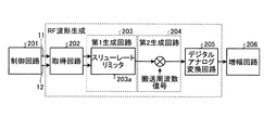
図1及び図2を用いて、第1の実施形態に係る磁気共鳴イメージング装置の全体構成について説明する。図1は、第1の実施形態に係る磁気共鳴イメージング装置の構成を示すブロック図である。図2は、実施形態に係るRFパルス生成回路の構成を示すブロック図である。すなわち、図2は、図1におけるRFパルス生成回路200をより詳細に説明した図である。
(First Embodiment)
The overall configuration of the magnetic resonance imaging apparatus according to the first embodiment will be described with reference to FIGS. 1 and 2. FIG. 1 is a block diagram showing a configuration of a magnetic resonance imaging apparatus according to the first embodiment. FIG. 2 is a block diagram showing a configuration of an RF pulse generation circuit according to an embodiment. That is, FIG. 2 is a diagram illustrating the RF
図1に示すように、磁気共鳴イメージング装置100は、静磁場磁石101と、シムコイル130と、傾斜磁場コイル102と、傾斜磁場電源103と、寝台104と、寝台制御回路105と、送信コイル106と、送信回路107と、受信コイル108と、受信回路109と、シーケンス制御回路110と、計算機システム120と、RFパルス生成回路200を備える。なお、磁気共鳴イメージング装置100に被検体P(例えば、人体)は含まれない。
As shown in FIG. 1, the magnetic
静磁場磁石101は、中空の円筒形状に形成された磁石であり、内部の空間に一様な静磁場を発生する。静磁場磁石101は、例えば、永久磁石、超伝導磁石等である。
The static
シムコイル130は、静磁場磁石101の内側において中空の円筒形状に形成されたコイルであり、図示されないシムコイル電源に接続され、シムコイル電源から供給される電源により、静磁場磁石101が発生した静磁場を均一化する。
The
傾斜磁場コイル102は、中空の円筒形状に形成されたコイルであり、静磁場磁石101及びシムコイル130の内側に配置される。傾斜磁場コイル102は、図2に示されているように、互いに直交するX,Y,Zの各軸に対応する3つのコイル(X軸傾斜磁場コイル102x、Y軸傾斜磁場コイル102y、Z軸傾斜磁場コイル102z)が組み合わされて形成されており、これら3つのコイルは、傾斜磁場電源103から個別に電流を受けて、X,Y,Zの各軸に沿って磁場強度が変化する傾斜磁場を発生させる。なお、Z軸方向は、静磁場と同方向とする。また、Y軸方向は、鉛直方向とし、X軸方向は、Z軸及びY軸に垂直な方向とする。
The gradient
なお、傾斜磁場コイル102によって発生するX,Y,Z各軸の傾斜磁場は、例えば、スライス選択用傾斜磁場Gs、位相エンコード用傾斜磁場Ge、及びリードアウト用傾斜磁場Grを形成する。スライス選択用傾斜磁場Gsは、任意に撮像断面を決めるために利用される。位相エンコード用傾斜磁場Geは、空間的位置に応じてMR信号の位相を変化させるために利用される。リードアウト用傾斜磁場Grは、空間的位置に応じてMR信号の周波数を変化させるために利用される。
The gradient magnetic fields of the X, Y, and Z axes generated by the gradient
傾斜磁場電源103は、傾斜磁場コイル102に電流を供給する。
The gradient magnetic
寝台104は、被検体Pが載置される天板104aを備え、寝台制御回路105による制御のもと、天板104aを、被検体Pが載置された状態で撮像口内へ挿入する。通常、寝台104は、長手方向が静磁場磁石101の中心軸と平行になるように設置される。寝台制御回路105は、計算機システム120による制御のもと、寝台104を駆動して天板104aを長手方向及び上下方向へ移動する。
The
送信コイル106は、傾斜磁場コイル102の内側に配置され、送信回路107からRF(Radio Frequency)パルスの供給を受けて、高周波磁場を発生する。送信回路107は、対象とする原子核の種類及び磁場の強度で決まるラーモア周波数に対応するRFパルスを送信コイル106に供給する。
The
受信コイル108は、傾斜磁場コイル102の内側に配置され、高周波磁場の影響によって被検体Pから発せられるMR信号を受信する。受信コイル108は、MR信号を受信すると、受信したMR信号を受信回路109へ出力する。例えば、受信コイル108は、1以上、典型的には複数のコイルエレメントを有するコイルアレイである。
The
受信回路109は、受信コイル108から出力されるMR信号に基づいてMRデータを生成する。具体的には、受信回路109は、受信コイル108から出力されるMR信号に対して、前置増幅、中間周波変換、位相検波、低周波増幅、フィルタリング等の各種信号処理を施した後、各種信号処理が施されたデータに対してアナログ/デジタル変換する。これにより、受信回路109は、デジタル化された複素数データであるMRデータを生成する。受信回路109が生成したMRデータは、生データとも呼ばれる。
The
また、受信回路109は、生成したMRデータをシーケンス制御回路110へ送信する。なお、受信回路109は、静磁場磁石101や傾斜磁場コイル102等を備える架台装置側に備えられていてもよい。
Further, the
ここで、第1の実施形態において、受信コイル108の各コイルエレメントから出力されるMR信号は、適宜分配合成されることで、チャネル等と呼ばれる単位で受信回路109に出力される。このため、MRデータは、受信回路109以降の後段の処理においてチャネル毎に取り扱われる。
Here, in the first embodiment, the MR signals output from each coil element of the receiving
コイルエレメントの総数とチャネルの総数との関係は、同一の場合もあれば、コイルエレメントの総数に対してチャネルの総数が少ない場合、あるいは反対に、コイルエレメントの総数に対してチャネルの総数が多い場合もある。なお、分配合成のタイミングは、上述したタイミングに限られるものではない。MR信号若しくはMRデータは、後述する画像生成機能122による処理の前までに、チャネル単位に分配合成されればよい。 The relationship between the total number of coil elements and the total number of channels may be the same, the total number of channels is small relative to the total number of coil elements, or conversely, the total number of channels is large relative to the total number of coil elements. In some cases. The timing of distribution synthesis is not limited to the above-mentioned timing. The MR signal or MR data may be distributed and synthesized in channel units before processing by the image generation function 122 described later.
シーケンス制御回路110は、計算機システム120から送信される撮像シーケンスの情報に基づいて、傾斜磁場電源103、送信回路107及び受信回路109を駆動することによって、被検体Pの撮像を行う。
The
撮像シーケンスとは、磁気共鳴イメージング装置100による検査に含まれる複数のプロトコルそれぞれに対応するパルスシーケンスを指す。撮像シーケンスの情報には、傾斜磁場電源103が傾斜磁場コイル102に供給する電源の強さや電源を供給するタイミング、送信回路107が送信コイル106に送信するRFパルスの強さやRFパルスを印加するタイミング、受信回路109がMR信号を検出するタイミング等が定義される。
The imaging sequence refers to a pulse sequence corresponding to each of a plurality of protocols included in the inspection by the magnetic
なお、シーケンス制御回路110は、傾斜磁場電源103、送信回路107及び受信回路109、シムコイル電源等を駆動して被検体Pを撮像した結果、受信回路109からMRデータを受信すると、受信したMRデータを計算機システム120へ転送する。
The
計算機システム120は、磁気共鳴イメージング装置100の全体制御や、データ収集、画像生成等を行う。計算機システム120は、処理回路150、記憶回路123、入力装置124、ディスプレイ125を備える。また、処理回路150は、インタフェース機能121、画像生成機能122、制御機能126を有する。
The
インタフェース機能121、画像生成機能122、制御機能126にて行われる各処理機能は、コンピュータによって実行可能なプログラムの形態で記憶回路123へ記憶されている。処理回路150はプログラムを記憶回路123から読み出し、実行することで各プログラムに対応する機能を実現するプロセッサである。換言すると、各プログラムを読みだした状態の処理回路150は、図1の処理回路150内に示された各機能を有することになる。なお、図1においては単一の処理回路150にて、インタフェース機能121、画像生成機能122、制御機能126にて行われる処理機能が実現されるものとして説明したが、複数の独立したプロセッサを組み合わせて処理回路150を構成し、各プロセッサがプログラムを実行することにより機能を実現するものとしても構わない。
Each processing function performed by the interface function 121, the image generation function 122, and the control function 126 is stored in the
換言すると、上述のそれぞれの機能がプログラムとして構成され、1つの処理回路が各プログラムを実行する場合であってもよいし、特定の機能が専用の独立したプログラム実行回路に実装される場合であってもよい。 In other words, each of the above-mentioned functions may be configured as a program, and one processing circuit may execute each program, or a specific function may be implemented in a dedicated and independent program execution circuit. You may.
上記説明において用いた「プロセッサ」という文言は、例えば、CPU(Central Processing Unit)、GPU(Graphical Processing Unit)或いは、特定用途向け集積回路(Application Specific Integrated Circuit:ASIC)、プログラマブル論理デバイス(例えば、単純プログラマブル論理デバイス(Simple Programmable Logic Device:SPLD)、複合プログラマブル論理デバイス(Complex Programmable Logic Device:CPLD)、及びフィールドプログラマブルゲートアレイ(Field Programmable Gate Array:FPGA))等の回路を意味する。プロセッサは記憶回路123に保存されたプログラムを読み出し実行することで機能を実現する。なお、記憶回路123にプログラムを保存する代わりに、プロセッサの回路内にプログラムを直接組み込むよう構成しても構わない。この場合、プロセッサは回路内に組み込まれたプログラムを読み出し実行することで機能を実現する。なお、寝台制御回路105、送信回路107、受信回路109、後述する図2のRFパルス生成回路200(例えば、制御回路201、取得回路202、第1生成回路203、スリューレートリミッタ203a、補間回路203b、フィルタ回路203c、第2生成回路204、デジタルアナログ変換回路205、増幅回路206、遅延補償回路207)等も同様に、上記のプロセッサなどの電子回路により構成される。
The term "processor" used in the above description refers to, for example, a CPU (Central Processing Unit), a GPU (Graphical Processing Unit), an integrated circuit for a specific application (Application Specific Integrated Circuit: ASIC), a programmable logic device (for example, a simple programmable logic device). A circuit of a programmable logic device (Simple Programmable Logic Device: SPLD), a composite programmable logic device (Complex Programmable Logic Device: CPLD), and a field programmable gate array (Field Programgable Gate Array: FPGA). The processor realizes the function by reading and executing the program stored in the
処理回路150は、インタフェース機能121により、撮像シーケンスの情報をシーケンス制御回路110へ送信し、シーケンス制御回路110からMRデータを受信する。また、処理回路150は、インタフェース機能121を通じて、MRデータを受信すると、受信したMRデータを記憶回路123に格納する。
The
処理回路150は、画像生成機能122により、インタフェース機能121を通じて受信したMRデータや、記憶回路123に保管されたデータを用いて、画像の生成を行う。なお、処理回路150は、画像生成機能122によって得られた画像は、必要に応じてディスプレイ125や記憶回路123に送信する。
The
処理回路150は、制御機能126により、磁気共鳴イメージング装置100の全体制御を行う。例えば、処理回路150は、制御機能126により、入力装置124を介して操作者から入力される撮像条件に基づいて撮像シーケンスの情報を生成し、生成した撮像シーケンスの情報をシーケンス制御回路110に送信することによって撮像を制御する。
The
記憶回路123は、処理回路150がインタフェース機能121を通じて受信したMRデータや、画像生成機能122により生成された画像データ等を記憶する。例えば、記憶回路123は、RAM(Random Access Memory)、フラッシュメモリ等の半導体メモリ素子、ハードディスク、光ディスク等である。
The
入力装置124は、操作者からの各種指示や情報入力を受け付ける。入力装置124は、例えば、マウスやトラックボール等のポインティングデバイス、あるいはキーボード等の入力デバイスである。
The
ディスプレイ125は、処理回路150における制御機能126による制御のもと、画像データ等の各種の情報を表示する。ディスプレイ125は、例えば、液晶表示器等の表示デバイスである。
The
RFパルス生成回路200は、計算機システム120、シーケンス制御回路110及び送信回路107等に接続され、計算機システム120から受信した命令や、シーケンス制御回路110から受信したシーケンスに関する情報に基づいて、RFパルスを生成し、生成したRFパルスを送信回路107に送信する回路である。RFパルス生成回路200のより詳細な構成は図2に示されている。図2は、実施形態に係るRFパルス生成回路の構成を示すブロック図である。
The RF
図2に示されているように、RFパルス生成回路200は、制御回路201、取得回路202、第1生成回路203、第2生成回路204、デジタルアナログ変換(DAC(Digital Analog Convertor)回路205)、増幅回路206、遅延補償回路207を備える。第1生成回路203は、スリューレートリミッタ203a、補間回路203b、フィルタ回路203cを備える。
As shown in FIG. 2, the RF
なお、取得回路202、第1生成回路203、第2生成回路204は、それぞれ取得部、第1生成部、第2生成部の一例である。
The
制御回路201は、例えばシーケンス制御回路110から、実行するパルスシーケンスに係る情報を取得し、取得したデータに基づいて、出力対象のRFパルスのエンベロープデータを、取得回路202に供給する回路である。取得回路202は、RFパルスのエンベロープデータを、制御回路201から取得する回路である。
The
第1生成回路203は、取得回路202が取得したRFパルスのエンベロープデータに対して、スリューレートリミッタ203a、補間回路203b、フィルタ回路203cのうち少なくとも一つの回路により所定の処理を行って、例えばスリューレートが小さくなったRFパルスのエンベロープデータである第2のデータを生成する回路である。第1生成回路203の行う処理の詳細については後述する。
The
第2生成回路204は、RFパルスのエンベロープデータにRFパルスの搬送波を加えて、RFパルスのデータを生成する回路である。デジタルアナログ変換(DAC)回路205は、デジタルアナログ変換処理を行ってデジタル信号をアナログ信号に変換する回路である。
The
増幅回路206は、例えばRFアンプであり、入力信号を増幅して、増幅された出力信号を出力する回路である。遅延補償回路207は、第2生成回路204においてエンベロープデータと搬送波とが望ましいタイミングで加算されるように、第1生成回路203の行う処理に要する時間を考慮した遅延補償処理を行うための回路である。遅延補償回路207の処理については後述する。
The
以上のように、実施形態に係る磁気共鳴イメージング装置100の全体構成について説明した。続いて、実施形態に係る磁気共鳴イメージング装置100に係る背景について簡単に説明する。
As described above, the overall configuration of the magnetic
磁気共鳴イメージング装置において、RF(Radio Frequency)パルスを生成するために、例えばDDS(Direct Digital Synthesizer)等の送信技術が用いられることがある。かかる場合、まず出力予定のRFパルスのエンベロープに関するデジタルデータが、RFパルスのベースバンドの周波数帯域により定められる一定の時間間隔(例えば1μ秒間隔等)で生成され、生成された一定の時間間隔のデジタルデータを基に、RFパルスが生成される。 In a magnetic resonance imaging apparatus, a transmission technique such as a DDS (Direct Digital Synthesizer) may be used to generate an RF (Radio Frequency) pulse. In such a case, first, digital data regarding the envelope of the RF pulse to be output is generated at a fixed time interval (for example, 1 μsec interval) determined by the frequency band of the baseband of the RF pulse, and the generated constant time interval RF pulses are generated based on digital data.
しかし、DDSを用いて、例えばUTE(ultrashot TE)等、ベースバンド周波数の大きい、すなわち短期間に値が大きく変化するパルスを生成しようとすると、前述のデジタルデータ一つ一つの波高値が大きくなり、スリューレート(信号値の時間変化率)が大きくなる。スリューレートの高い入力がRFアンプに入力されると、過渡現象によりRFパルスの出力が増加(オーバーシュート)し、RFアンプに対する負荷が増大する。なお、RFパルスの波高の立ち上がりを単純になだらかにしてしまうのでは、本来出力したいRF波形を出せないことがある。 However, if DDS is used to generate a pulse having a large baseband frequency, that is, a value that changes significantly in a short period of time, such as UTE (ultrashot TE), the peak value of each of the above-mentioned digital data becomes large. , The slew rate (time change rate of signal value) becomes large. When an input with a high slew rate is input to the RF amplifier, the output of the RF pulse increases (overshoots) due to the transient phenomenon, and the load on the RF amplifier increases. If the rise of the wave height of the RF pulse is simply smoothed, it may not be possible to output the RF waveform that is originally desired to be output.
かかる状況について、図3〜図6を用いて説明する。図3〜図6は、第1の実施形態に係る磁気共鳴イメージング装置の背景について説明した図である。 Such a situation will be described with reference to FIGS. 3 to 6. 3 to 6 are views for explaining the background of the magnetic resonance imaging apparatus according to the first embodiment.
図3は、増幅回路206の典型的な応答をモデル化したものである。時刻をtとし、図3に示されているように、入力信号をf(t)とし、アンプの増幅率をAとし、帰還回路の減衰率をHとすると、出力信号F(t)は、F(t)=(1/(H+1/A))×f(t)とあらわされる。入力信号が時間依存する場合、入力信号f(t)のスリューレートが高い場合、出力信号F(t)が、過渡応答を示す場合がある。
FIG. 3 models the typical response of
図4は、入力信号のスリューレートが「小」の場合の、出力信号の時間変化の一例である。横軸は時刻を表し、縦軸は出力信号の振幅を表す。かかる場合入力信号のスリューレートが「小」であるので、帰還により、出力信号が短時間で安定する。 FIG. 4 is an example of a time change of the output signal when the slew rate of the input signal is “small”. The horizontal axis represents the time and the vertical axis represents the amplitude of the output signal. In such a case, since the slew rate of the input signal is “small”, the output signal is stabilized in a short time by feedback.
一方、図5は、入力信号のスリューレートが「大」の場合の、出力信号の時間変化の一例である。横軸は時刻を表し、縦軸は出力信号の振幅を表す。かかる場合、アンプの増幅率と帰還回路のインピーダンスによっては、出力信号が安定せず、過渡現象が生じる。 On the other hand, FIG. 5 is an example of a time change of the output signal when the slew rate of the input signal is “large”. The horizontal axis represents the time and the vertical axis represents the amplitude of the output signal. In such a case, the output signal is not stable and a transient phenomenon occurs depending on the amplification factor of the amplifier and the impedance of the feedback circuit.
このように、過渡現象が生じると、増幅回路206が破損しやすくなったり、または保護回路が作動することにより、システムダウンが生じたりすることがある。従って、増幅回路206への入力信号のスリューレートは増幅回路206に適した値となることが望ましい。
As described above, when a transient phenomenon occurs, the
図6は、DDSにより生成される信号データと、RFアンプへと出力されるデータとの関係の典型例を示している。横軸は時刻を表し、縦軸は信号強度を表す。データ信号50a、50b、50c、50d、50e、50f、50g、50h、50iは、DDSにより生成されるRFパルスのエンベロープデータを表す。実線で示されている波形1は、RFパルスのエンベロープデータを基に生成され、後段の回路に出力される波形の典型例を示している。 FIG. 6 shows a typical example of the relationship between the signal data generated by the DDS and the data output to the RF amplifier. The horizontal axis represents time and the vertical axis represents signal strength. The data signals 50a, 50b, 50c, 50d, 50e, 50f, 50g, 50h, 50i represent the envelope data of the RF pulse generated by the DDS. The waveform 1 shown by the solid line shows a typical example of the waveform generated based on the envelope data of the RF pulse and output to the circuit in the subsequent stage.
DDSにより生成されるエンベロープデータは、図6に例示されているように、例えば一定の時間間隔(例えば1μs)で生成される。ハードウェアの制限から、これらのエンベロープデータの転送速度に上限があるので、エンベロープデータの時間間隔は、例えば所定の時間間隔を下回らない。かかる場合、エンベロープデータを基に生成される波形は、例えば波形1のように、矩形状になり、スリューレートが大きい波形になる。このような波形がRFアンプに入力されると、RFアンプの負荷が大きいことから、RFアンプに入力される波形は、RFアンプが応答可能なスリューレート、すなわち、スリューレートが小さい波形であることが望ましい。 The envelope data generated by DDS is generated, for example, at regular time intervals (for example, 1 μs), as illustrated in FIG. Due to hardware limitations, there is an upper limit to the transfer speed of these envelope data, so the time interval of the envelope data does not fall below, for example, a predetermined time interval. In such a case, the waveform generated based on the envelope data has a rectangular shape, such as waveform 1, and has a large slew rate. When such a waveform is input to the RF amplifier, the load on the RF amplifier is large. Therefore, the waveform input to the RF amplifier is a slew rate that the RF amplifier can respond to, that is, a waveform with a small slew rate. It is desirable to have.
次に、図7を用いて、スリューレートリミッタを用いない場合の、RFパルス生成回路200の行う処理の流れについて説明する。図7は、スリューレートリミッタを用いない場合の磁気共鳴イメージング装置100の構成について説明した図である。
Next, with reference to FIG. 7, the flow of processing performed by the RF
図7において、制御回路201、取得回路202、第2生成回路204、デジタルアナログ変換回路205、増幅回路206は、それぞれ図2の制御回路201、取得回路202、第2生成回路204、デジタルアナログ変換回路205、増幅回路206に対応する。矢印10は、RF波形のエンベロープデータの流れを表す。
In FIG. 7, the
まず、制御回路201は、シーケンス制御回路110から、実行するパルスシーケンスに係る情報を取得する。一方、制御回路201は、計算機システム120から、例えばユーザの命令のなどの情報を取得する。制御回路201が取得する情報の一例としては、例えば、出力対象のRFパルスのエンベロープの種類を表す情報(例えば、どのような形のエンベロープであるか)、出力対象のRFパルスのエンベロープに関するパラメータ(例えば、波高、印加タイミング、印加時間等)、出力対象のRFパルスの搬送波に関するパラメータ(例えば、ラーモア周波数、搬送波の強度)、RFアンプの電気的特性に関するパラメータ、スリューレートの上限値等の情報である。続いて、制御回路201は、矢印10に示されているように、RFパルスのエンベロープに関する情報を取得回路202に出力する。前述したように、ハードウェアの制限から、これらのエンベロープデータの転送速度に上限があるので、エンベロープデータの時間間隔は、例えば所定の時間間隔を下回らない時間間隔となる。
First, the
取得回路202は、制御回路201から、RFパルスのエンベロープに関する情報を取得する。取得回路202は、取得したRFパルスのエンベロープに関する情報に基づいて、RFパルスのエンベロープ信号を生成し、生成したRFパルスのエンベロープ信号を、第2生成回路204に出力する。例えば、取得回路202は、図6のデータ信号50a、50b、50c、50d、50e、50f、50g、50h、50iをRFパルスのエンベロープに関する情報として制御回路201から取得し、波形1を第2生成回路204に出力する。
The
続いて、第2生成回路204は、入力されたエンベロープ信号を、搬送周波数信号にのせて、RFパルスの信号を生成し、生成した信号を、デジタルアナログ変換回路205に出力する。デジタルアナログ変換回路205は、デジタルデータである入力された信号を、アナログ信号に変換し、増幅回路206に出力する。増幅回路206は、入力されたアナログ信号を増幅し、出力された信号を、送信回路107に出力する。
Subsequently, the
スリューレートリミッタを用いない場合の構成の場合、前述のように、RFアンプの付加が大きくなりうる。かかる背景に鑑みて、実施形態に係るRFパルス生成回路200は、RFパルスのエンベロープデータと、パルスの満たすべきスリューレートの値の上限値とに基づいて、スリューレートの最大値が低減されたエンベロープデータを生成する。これにより、データの波高を大きく保ったまま、スリューレートを低減することができ、この結果RFアンプに対する負荷を軽減させることができる。
In the case of the configuration without the slew rate limiter, the addition of the RF amplifier can be large as described above. In view of this background, in the RF
かかる構成について、図8、図10、図11を適宜参照しながら、図9を用いて説明する。図8は、第1の実施形態に係る磁気共鳴イメージング装置100の構成について説明した図である。図9は、第1の実施形態に係る磁気共鳴イメージング装置100の行う処理の流れについて説明したフローチャートである。図10及び図11は、第1の実施形態に係る磁気共鳴イメージング装置100の行う処理について説明した図である。
Such a configuration will be described with reference to FIG. 9, with reference to FIGS. 8, 10, and 11. FIG. 8 is a diagram illustrating the configuration of the magnetic
図8において、制御回路201、取得回路202、第1生成回路203、スリューレートリミッタ203a、第2生成回路204、デジタルアナログ変換回路205、増幅回路206は、それぞれ図2の制御回路201、取得回路202、第1生成回路203、スリューレートリミッタ203a、第2生成回路204、デジタルアナログ変換回路205、増幅回路206に対応する。矢印11は、RF波形エンベロープデータの流れを表す。矢印12は、スリューレート上限値の情報の流れを表す。
In FIG. 8, the
はじめに、制御回路201は、シーケンス制御回路110から、実行するパルスシーケンスに係る情報を取得する。また、制御回路201は、計算機システム120から、例えばユーザの命令などの情報を取得する。制御回路201が取得する情報の一例としては、すでに述べたように、例えば、出力対象のRFパルスのエンベロープの種類を表す情報(例えば、どのような形のエンベロープであるか)、出力対象のRFパルスのエンベロープに関するパラメータ(例えば、波高、印加タイミング、印加時間等)、出力対象のRFパルスの搬送波に関するパラメータ(例えば、ラーモア周波数、搬送波の強度)、RFアンプの電気的特性に関するパラメータ、後述する第1のデータから生成されるデータ列の満たすべきスリューレートの上限値の値等の情報である。制御回路201は、取得した情報に基づいて、出力するRFパルスのエンベロープに関する情報を含む第1のデータを生成する(ステップS100)。制御回路201は、取得回路202に対して、矢印11に示されているように、出力するRFパルスのエンベロープに関する情報を含む第1のデータを出力する。また、制御回路201は、取得回路202に対して、矢印12に示されているように、スリューレートの上限値の値を出力する。
First, the
続いて、取得回路202は、出力するRFパルスのエンベロープに関する情報を含む第1のデータを取得する(ステップS110)。例えば、取得回路202は、図6のデータ信号50a、50b、50c、50d、50e、50f、50g、50h、50iを、出力するRFパルスのエンベロープに関する情報として制御回路201から取得する。続いて、第1生成回路203は、取得回路202がステップS110において取得した第1のデータと、第1のデータから生成されるデータ列の満たすべきスリューレートの上限値の値とに基づいて、第2のデータを生成する(ステップS120)。
Subsequently, the
具体的には、ステップS120の処理が行われなかった場合、生成される第2のデータの波形は、後述する図10の波形1のように、例えば階段関数のような形状となり、スリューレートが大きくなる。従って、第1生成回路203は、ステップS120の処理を行うことにより、生成される第2のデータの波形のスリューレートを低減することができる。なお、第1生成回路203においては、ハードウェアなどにおける制限がDDSに比較して緩やかであるので、取得回路202が取得したエンベロープに関する情報の時間間隔(例えばデータ信号50aとデータ信号50bとの時間間隔)より短い時間間隔に対して、データ処理を行うことができる。
Specifically, when the process of step S120 is not performed, the waveform of the generated second data has a shape like, for example, a step function, as shown in waveform 1 of FIG. 10 described later, and the slew rate. Becomes larger. Therefore, the
まず、ステップS120の処理の第1の例として、図8に示されているように、第1生成回路203が、スリューレートリミッタ203aを用いて第2のデータを生成する場合について説明する。すなわち、第1生成回路203は、スリューレートリミッタ203aを用いた処理を第1のデータに対して行うことにより、スリューレートが取得したスリューレートの上限値の値を超えないようなデータである第2のデータを生成する。
First, as a first example of the process of step S120, a case where the
スリューレートリミッタ203aの例示的な構成としては、スリューレートリミッタ203aは、入力信号のスリューレートの大きさを検出する検出回路と、大きいスリューレートが検出されたとき、入力信号に対してネガティブフィードバックをかける(または検出された信号を除去する)フィードバック回路とからなる。検出回路、フィードバック回路は、それぞれ例えばアナログ回路におけるコイル、及び作動増幅器に対応するデジタル回路である。スリューレートリミッタ203aは、例えば所定のスリューレートの上限値を超えた信号を完全にカットしてもよいし、また所定のスリューレートの上限値を超えた信号の大きさを抑制してもよい。この結果、スリューレートリミッタ203aは、第1のデータと比較してスリューレートの大きさが小さくなったデータである第2のデータを出力する。
As an exemplary configuration of the
次に、ステップS120の処理の第2の例として、図10及び図11を用いて、第1生成回路203が、補間回路203bを用いて第2のデータを生成する場合について説明する。
Next, as a second example of the processing in step S120, a case where the
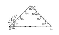
図10において、横軸は時刻を表し、縦軸は信号強度を表す。図6と同様に、データ信号50a、50b、50c、50d、50e、50f、50g、50h、50iは、出力予定のRFパルスのエンベロープに関する情報を含む第1のデータのデータ点一つ一つを表している。波形1は、補間処理がなかったと仮定した場合に出力されるデータを表す。点線は、第1生成回路203が第1のデータに対して補間処理を含んだ処理を行って生成した第2のデータを表している。線分70、線分71、線分72、線分73、線分74、線分75、線分76、線分77は、点線の一部分をそれぞれ取り出したものである。第2のデータは、例えば図11に示された補間処理に基づいて生成される。
In FIG. 10, the horizontal axis represents time and the vertical axis represents signal strength. Similar to FIG. 6, the data signals 50a, 50b, 50c, 50d, 50e, 50f, 50g, 50h, 50i each data point of the first data including information about the envelope of the RF pulse to be output. Represents. Waveform 1 represents data that is output when it is assumed that there is no interpolation processing. The dotted line represents the second data generated by the
図11において、横軸は時刻を表し、縦軸は信号強度を表す。図6と同様に、データ信号50a、50b、50c、50d、50e、50f、50g、50h、50i等の黒丸は、出力予定のRFパルスのエンベロープに関する情報を含む第1のデータのデータ点一つ一つを表している。点51a、点51b、点51c、点51d、点51e、51f、点51g等の白丸は、補間処理が行われた点を表している。区間61、区間62、及び区間63は、それぞれデータ信号50b、50e、50fから、データ信号50c、50f、50gまでの時間区間を示している。
In FIG. 11, the horizontal axis represents time and the vertical axis represents signal strength. Similar to FIG. 6, the black circles of the data signals 50a, 50b, 50c, 50d, 50e, 50f, 50g, 50h, 50i, etc. are one data point of the first data including the information about the envelope of the RF pulse to be output. It represents one. White circles such as
ステップS120において、第1生成回路203は、データ信号を取得回路202を通じて取得すると、現に取得したデータ点と、その前に取得したデータ点との間で補間処理を行う。例えば、第1生成回路203は、データ信号50aとデータ信号50bとを取得すると、データ信号50aとデータ信号50bとの間に線形補間を行って、点51a、点51b、点51c、点51d、点51e、点51f、点51g等の点を生成する。
In step S120, when the
続いて、第1生成回路203は、行われた補間処理の結果に基づいて、スリューレートの大きさが低減されたデータである第2のデータを生成する。例えば、データ信号50bの時刻〜データ信号50cの時刻において、第1生成回路203は、行われた補間処理の結果に基づいて、例えば線分70のように、信号値の大きさが目標値であるデータ信号50bの大きさに達するまで、ゆるやかに信号値の大きさが増加していくようなデータを第2のデータとして生成する。第1生成回路203は、線分70の傾きを、例えば、点51gとデータ信号50bとを結ぶ直線の傾きとする。別の例として、第1生成回路203は、線分70の傾きを、例えば、データ信号50aとデータ信号50bとを結ぶ直線の傾きとする。信号値の大きさが目標値であるデータ信号50bの大きさに達すると、第1生成回路203は、線分71のように信号値をデータ信号50bの値で固定するようなデータを第2のデータとして生成する。
Subsequently, the
同様に、データ信号50cの時刻〜データ信号50dの時刻において、第1生成回路203は、区間61における補間処理の結果に基づいて、例えば線分72のように、信号値の大きさが目標値であるデータ信号50cの大きさに達するまで、ゆるやかに信号値の大きさが増加していくようなデータを第2のデータとして生成する。信号値の大きさが目標値であるデータ信号50cに達すると、第1生成回路203は、線分73のように信号値をデータ信号50cの値で固定するようなデータを第2のデータとして生成する。
Similarly, from the time of the data signal 50c to the time of the data signal 50d, the
同様に、データ信号50fの時刻〜データ信号50gの時刻において、第1生成回路203は、区間62における補間処理の結果に基づいて、例えば線分74のように、信号値の大きさが目標値であるデータ信号50fの大きさに達するまで、ゆるやかに信号値の大きさが減少していくようなデータを第2のデータとして生成する。信号値の大きさが目標値であるデータ信号50fに達すると、第1生成回路203は、線分75のように信号値をデータ信号50fの値で固定するようなデータを第2のデータとして生成する。
Similarly, from the time of the data signal 50f to the time of the
同様に、データ信号50gの時刻〜データ信号50hの時刻において、第1生成回路203は、区間63における補間処理の結果に基づいて、例えば線分76のように、信号値の大きさが目標値であるデータ信号50gの大きさに達するまで、ゆるやかに信号値の大きさが減少していくようなデータを第2のデータとして生成する。信号値の大きさが目標値であるデータ信号50gに達すると、第1生成回路203は、線分77のように信号値をデータ信号50gの値で固定するようなデータを第2のデータとして生成する。
Similarly, from the time of the data signal 50g to the time of the data signal 50h, the
このように、第1生成回路203は、第1のデータに対して補間処理を含んだ処理を行って、第2のデータを生成する。
In this way, the
なお、補間処理は線形補間に限られず、対数補間、指数補間、スプライン補間、ラグランジュ補間等、他の種類の補間が用いられてもよい。また、第1生成回路203は、第1のデータの種類に応じた補間処理を含んだ処理を行って、第2のデータを生成してもよい。ここで、第1のデータの種類とは、例えばパルスシーケンスの種類や、生成される第1のデータの時間間隔の大小等を意味する。例えば、第1生成回路203は、信号値が大きく変化するような波形の場合には対数補間を用い、通常の波形の場合には線形補間を用いる。また、別の例として、第1生成回路203は、波形に対して高精度が要求される場合にはスプライン補間を用い、通常の場合には線形補間を用いる。
The interpolation process is not limited to linear interpolation, and other types of interpolation such as logarithmic interpolation, exponential interpolation, spline interpolation, and Lagrange interpolation may be used. Further, the
次に、ステップS120の処理の第3の例として、第1生成回路203が、フィルタ回路203cを用いて第2のデータを生成する場合について説明する。すなわち、第1生成回路203は、第1のデータに対してフィルタ処理を含んだ処理を行って、第2のデータを生成する。
Next, as a third example of the processing in step S120, a case where the
ここで、フィルタ回路203cの具体例としては、例えばスムージングフィルタや移動平均フィルタの処理を行うフィルタ回路である。また、フィルタ回路203cの別の具体例としては、ローパスフィルタとして機能するフィルタ回路であってもよい。
Here, as a specific example of the
また、第1生成回路203は、第1のデータの種類に応じたフィルタ処理を含んだ処理を行って、第2のデータを生成する。前述のように、第1のデータの種類の具体例としては、例えばパルスシーケンスの種類や、生成される第1のデータの時間間隔の大小等が挙げられる。かかる処理の一例として、例えば、第1生成回路203は、第1のデータの種類に応じて、ローパスフィルタのカットオフ周波数を変化させる。
Further, the
このように、ステップS120の処理が完了すると、第1生成回路203は、第2生成回路204に、生成した第2のデータを出力する。続いて、第2生成回路204は、第1生成回路203が生成した第2のデータと、出力するRFパルスの搬送波に関する情報とに基づいて、RFパルスの信号を生成する(ステップS130)。
As described above, when the process of step S120 is completed, the
続いて、デジタルアナログ変換回路205は、生成されたRFパルスの信号に対してデジタルアナログ変換(DAC)を行いアナログデータを生成し、変換後のアナログデータをRFアンプ(増幅回路206)に出力する。(ステップS140)。RFアンプ(増幅回路206)は、変換後のアナログデータを増幅して、RFパルスを生成する(ステップS150)。換言すると、第2生成回路204が、RFパルスの信号をデジタルデータで生成した後、デジタルアナログ変換が行われ、変化後のアナログデータが、RFアンプ(増幅回路206)に出力される。なお、エンベロープのデータと搬送波のデータを合わせたRFパルスをデジタルデータで生成する場合は、エンベロープのデータのみをデジタルデータで生成し、デジタルアナログ変換を行ったあとアナログで搬送波と合成してRFパルスを生成する場合と比較して、出力波形が安定しやすいという利点がある。
Subsequently, the digital-to-
以上のように、第1の実施形態の磁気共鳴イメージング装置100によれば、RFアンプに対する負荷を軽減させながらRFパルスを生成することができる。より具体的には、例えば、スリューレートの大きい信号が増幅回路206(RFアンプ)に入力されることにより、オーバーシューティング等により不要なパルスが発生することを抑制することができる。また、パルス幅の短いパルスを出力する場合においても、パルスの立ち上がり速度を遅くすることなく、安定したRFパルスの波形を出力することができる。なお、例えば傾斜磁場波形を生成する場合と比較して、RFパルスを生成する場合においては、スリューレートリミッタを用いた処理に加えて、エンベロープデータを搬送波に乗せる処理が、スリューレートリミッタを用いた処理の後に行われる。
As described above, according to the magnetic
実施形態はこれに限られない。一例として、RFアンプに出力可能なスリューレートの最大値は、RFアンプごと(例えば、製造メーカーやRFアンプの型番)に異なっている。従って、ステップS120において、第1生成回路203は、ステップS140において出力するRFアンプの電気的特性に応じた、スリューレートの上限値の値に基づいて、第2のデータを生成してもよい。かかる構成を用いることにより、RFアンプの特性に応じて、RFアンプの入力を最適化することができる。
The embodiment is not limited to this. As an example, the maximum value of the slew rate that can be output to the RF amplifier differs for each RF amplifier (for example, the manufacturer and the model number of the RF amplifier). Therefore, in step S120, the
また、ステップS120における処理については、所定の処理時間を要するので、第2のデータの波形は、第1のデータに比較して、所定の遅延時間を伴ったものになる。従って、これらの遅延時間を考慮して、ステップS130の処理が行われてもよい。具体的には、ステップS130において、第2生成回路204は、第1生成回路203が第2のデータを生成するのに要する時間である遅延時間を補償する処理を含んで、RFパルスの信号を生成してもよい。換言すると、第2生成回路204は、例えば、遅延時間分だけ、搬送波のデータをエンベロープデータに比較して遅らせて入力する。または、第1生成回路203は、遅延時間分だけ、エンベロープデータを、搬送波のデータに比較して早めてスリューレートリミッタ203aに入力してもよい。上述の遅延時間の値については、RFパルスの生成を開始する前に予め与えられていてもよいし、RFパルス生成回路200が、ステップS130の処理までに、遅延時間の値を計算してもよい。
Further, since the processing in step S120 requires a predetermined processing time, the waveform of the second data is accompanied by a predetermined delay time as compared with the first data. Therefore, the process of step S130 may be performed in consideration of these delay times. Specifically, in step S130, the
なお、遅延時間を考慮する処理については、後述の変形例についても同様に適用可能である。 The process of considering the delay time can be similarly applied to the modification described later.
(第1の実施形態の第1の変形例)
第1の実施形態では、ステップS130において、第2生成回路204が、第2のデータと、搬送波の情報に基づいて、RFパルスの信号をデジタル的に生成したのち、デジタルアナログ変換回路205がデジタルアナログ変換を行ってアナログデータを生成する場合について説明した。実施形態はこれに限られない。第1の実施形態の第1の変形例では、デジタルアナログ変換回路205が、デジタルデータである第2のデータに対してデジタルアナログ変換を行ってアナログデータを生成したのち、第2生成回路204が、アナログ的にエンベロープデータと搬送波のデータを合成してRFパルスの信号を生成する。
(First modification of the first embodiment)
In the first embodiment, in step S130, the
図12は、第1の実施形態の第1の変形例に係る磁気共鳴イメージング装置の構成について説明した図である。図13は、第1の実施形態の第1の変形例に係る磁気共鳴イメージング装置の行う処理の流れについて説明した図である。 FIG. 12 is a diagram illustrating a configuration of a magnetic resonance imaging apparatus according to a first modification of the first embodiment. FIG. 13 is a diagram illustrating a flow of processing performed by the magnetic resonance imaging apparatus according to the first modification of the first embodiment.
図12において、制御回路201、取得回路202、第1生成回路203、スリューレートリミッタ203a、第2生成回路204、増幅回路206は、それぞれ図2の制御回路201、取得回路202、第1生成回路203、スリューレートリミッタ203a、第2生成回路204、増幅回路206に対応する。図12のデジタルアナログ変換回路205は、図2のデジタルアナログ変換回路205と同様の処理を行う回路である。矢印13は、RF波形エンベロープデータを表す。矢印14は、スリューレート上限値の情報を表す。
In FIG. 12, the
図13において、ステップS200、ステップS210、ステップS220及びステップS250は、図9のステップS100、ステップS110、ステップS120及びステップS150に対応する。これらの処理については、第1の実施形態において既に説明したので繰り返しての説明は省略する。 In FIG. 13, step S200, step S210, step S220 and step S250 correspond to step S100, step S110, step S120 and step S150 of FIG. Since these processes have already been described in the first embodiment, the repeated description will be omitted.
ステップS220において、スリューレートリミッタ203aが第2のデータを生成すると、第1生成回路203は、デジタルアナログ変換回路205に、生成した第2のデータを出力する。続いて、デジタルアナログ変換回路205は、生成された第2のデータに対して、デジタルアナログ変換(DAC)を行いアナログデータを生成する(ステップS230)。デジタルアナログ変換回路は、生成したアナログデータを、第2生成回路204に出力する。続いて、第2生成回路204は、生成されたアナログデータと、出力するRFパルスの搬送波に関する情報に基づいて、RFパルスの信号を生成する(ステップS240)。第2生成回路204は、生成されたRFパルスの信号を、増幅回路206に入力する。
In step S220, when the
このように、第1の実施形態の第1の変形例では、第1の実施形態と同様に、RFアンプに対する負荷を軽減させながらRFパルスを生成することができる。 As described above, in the first modification of the first embodiment, as in the first embodiment, the RF pulse can be generated while reducing the load on the RF amplifier.
(第1の実施形態の第2の変形例)
第1の実施形態では、ステップS120において、第1生成回路203が、スリューレートリミッタ203aを用いて第2のデータを生成する場合について説明した。実施形態はこれに限られない。第1の実施形態の第2の変形例では、第1生成回路203が、ステップS120に対応するステップにおいて、スリューレートリミッタ203a、補間回路203b、フィルタ回路203cのうち2以上の回路を用いて第2のデータを生成する場合について説明する。スリューレートリミッタ203a、補間回路203b、フィルタ回路203cは、信号の安定性という関係から長所短所がそれぞれあることから、これらの回路を適宜組み合わせることで、より最終的な出力を安定させることが可能になる。
(Second variant of the first embodiment)
In the first embodiment, the case where the
図14は、第1の実施形態の第2の変形例に係る磁気共鳴イメージング装置の構成について説明した図である。図15は、第1の実施形態の第2の変形例に係る磁気共鳴イメージング装置の行う処理の流れについて説明したフローチャートである。 FIG. 14 is a diagram illustrating a configuration of a magnetic resonance imaging apparatus according to a second modification of the first embodiment. FIG. 15 is a flowchart illustrating a flow of processing performed by the magnetic resonance imaging apparatus according to the second modification of the first embodiment.
図14において、制御回路201、取得回路202、第1生成回路203、フィルタ回路203c、スリューレートリミッタ203a、デジタルアナログ変換回路205、第2生成回路204、増幅回路206は、それぞれ図2の制御回路201、取得回路202、第1生成回路203、フィルタ回路203c、スリューレートリミッタ203a、デジタルアナログ変換回路205、第2生成回路204、増幅回路206に対応する。矢印15及び矢印18は、RF波形エンベロープデータを表す。矢印16及び矢印19は、サンプリングピッチやRFパルスの波形種など、フィルタ回路203cが行う処理に使用される所定のパラメータを表す。矢印17及び矢印20は、スリューレート上限値の情報を表す。
In FIG. 14, the
図15において、ステップS300、ステップS310、ステップS340、ステップS350及びステップS260は、図9のステップS100、ステップS110、ステップS130、ステップS140及びステップS150に対応する。これらの処理については、第1の実施形態において既に説明したので繰り返しての説明は省略する。 In FIG. 15, step S300, step S310, step S340, step S350 and step S260 correspond to step S100, step S110, step S130, step S140 and step S150 of FIG. Since these processes have already been described in the first embodiment, the repeated description will be omitted.
ステップS310において、取得回路202が出力するRFパルスのエンベロープに関する情報を含む第1のデータを取得すると、続いて、第1生成回路203は、フィルタ回路203cにより、第1のデータに対して、例えばフィルタ処理を行うことにより、フィルタ処理が行われたデータを生成する(ステップS320)。この時、第1生成回路203は、矢印19で示されるように、取得回路202から取得した、サンプリングピッチやRFパルスの波形種に基づいて、ステップS320において適用するフィルタ処理の種類を選択し、選択したフィルタ処理に基づいて、フィルタ処理が行われたデータを作成する。
In step S310, when the first data including the information regarding the envelope of the RF pulse output by the
また、別の例として、ステップS320において、第1生成回路203は、補間回路203bにより、第1のデータに対して、補間処理を行うことにより、補間が行われたデータを生成してもよい。
Further, as another example, in step S320, the
続いて、第1生成回路203は、スリューレートリミッタ203aにより、生成されたデータと、スリューレートの上限値の値とに基づいて、第2のデータを生成する(ステップS330)。換言すると、第1生成回路203は、第1のデータに対してフィルタ処理(または補間処理)を行うことにより得られたデータと、スリューレートの上限値の値とに基づいて、第2のデータを生成する。第1生成回路203は、生成した第2のデータを、第2生成回路204に出力する。
Subsequently, the
なお、実施形態はこれらに限られない。例えば、補間回路203b、フィルタ回路203cと、スリューレートリミッタ203aの処理の順番は、上述した例に限られず、スリューレートリミッタ203aの処理の後、補間回路203b又はフィルタ回路203cで処理が行われても良い。また、補間回路203b、フィルタ回路203c、及びスリューレートリミッタ203aの3つの回路で処理が行われても良いし、スリューレートリミッタ203aで処理を行わず、補間回路203b及びフィルタ回路203cで処理が行われても良い。
The embodiments are not limited to these. For example, the order of processing of the interpolation circuit 203b, the
(その他の実施形態)
なお、実施形態はこれらに限られない。第1生成回路203が第1のデータを基に第2のデータを生成する処理を、デジタル処理を用いて行い、デジタルアナログ変換回路205が、アナログデータに変換する例について説明したが、実施形態はこれに限られず、第2のデータが生成される処理を、アナログ処理を用いて行ってもよい。換言すると、第1生成回路203は、アナログ回路を用いて、第1のデータと、スリューレートの上限値の値とに基づいて、第2のデータを生成してもよい。
(Other embodiments)
The embodiments are not limited to these. An example in which the
かかるアナログ回路の構成例としては、例えば、VGA(Varible Gate Amplifer)を用いた回路が挙げられる。VGAにおいては、信号の増幅率が、印加される電圧に依存するので、電圧を動的に制御することにより、ゲインを可変に制御することができる。ステップS120においてVGAが用いられる場合には、第1のデータが、DDSにおいて生成されたデジタルデータであることを要しない。 As a configuration example of such an analog circuit, for example, a circuit using VGA (Variable Gate Amplifier) can be mentioned. In VGA, the amplification factor of the signal depends on the applied voltage, so the gain can be variably controlled by dynamically controlling the voltage. When VGA is used in step S120, the first data does not need to be digital data generated in the DDS.
また、別の例として、RFパルス生成回路200は、ステップS110の後、ステップS120の処理に先立って、第1のデータに対して、オーバーシューティングを補償するための所定の補正処理を行い、補正処理が行われたあとのデータを、ステップS120の第1のデータとして取り扱っても良い。
Further, as another example, after step S110, the RF
(プログラム)
上述した実施形態の中で示した処理手順に示された指示は、ソフトウェアであるプログラムに基づいて実行されることが可能である。汎用の計算機システムが、このプログラムを予め記憶しておき、このプログラムを読み込むことにより、上述した実施形態の磁気共鳴イメージング装置100による効果と同様な効果を得ることも可能である。上述した実施形態で記述された指示は、コンピュータに実行させることのできるプログラムとして、磁気ディスク(フレキシブルディスク、ハードディスク等)、光ディスク(CD−ROM、CD−R、CD−RW、DVD−ROM、DVD±R、DVD±RW等)、半導体メモリ、又はこれに類する記録媒体に記録される。コンピュータ又は組み込みシステムが読み取り可能な記憶媒体であれば、その記憶形式は何れの形態であってもよい。コンピュータは、この記録媒体からプログラムを読み込み、このプログラムに基づいてプログラムに記述されている指示をCPUで実行させれば、上述した実施形態の磁気共鳴イメージング装置100と同様な動作を実現することができる。もちろん、コンピュータがプログラムを取得する場合又は読み込む場合はネットワークを通じて取得又は読み込んでもよい。
(program)
The instructions given in the processing procedure shown in the above-described embodiment can be executed based on a program that is software. By storing this program in advance in a general-purpose computer system and reading this program, it is possible to obtain an effect similar to the effect of the magnetic
また、記憶媒体からコンピュータや組み込みシステムにインストールされたプログラムの指示に基づきコンピュータ上で稼働しているOS(オペレーティングシステム)や、データベース管理ソフト、ネットワーク等のMW(ミドルウェア)等が、上述した実施形態を実現するための各処理の一部を実行してもよい。 In addition, the OS (operating system) running on the computer based on the instructions of the program installed in the computer or the embedded system from the storage medium, the database management software, the MW (middleware) of the network, etc. are the above-described embodiments. You may execute a part of each process to realize.
更に、記憶媒体は、コンピュータあるいは組み込みシステムと独立した媒体に限らず、LAN(Local Area Network)やインターネット等により伝達されたプログラムをダウンロードして記憶又は一時記憶した記憶媒体も含まれる。 Further, the storage medium is not limited to a medium independent of a computer or an embedded system, but also includes a storage medium in which a program transmitted by a LAN (Local Area Network), the Internet, or the like is downloaded and stored or temporarily stored.
また、記憶媒体は1つに限られず、複数の媒体から、上述した実施形態における処理が実行される場合も、実施形態における記憶媒体に含まれ、媒体の構成は何れの構成であってもよい。 Further, the storage medium is not limited to one, and even when the processing in the above-described embodiment is executed from a plurality of media, the storage medium in the embodiment is included, and the configuration of the medium may be any configuration. ..
なお、実施形態におけるコンピュータ又は組み込みシステムは、記憶媒体に記憶されたプログラムに基づき、上述した実施形態における各処理を実行するためのものであって、パソコン、マイコン等の1つからなる装置、複数の装置がネットワーク接続されたシステム等の何れの構成であってもよい。 The computer or embedded system in the embodiment is for executing each process in the above-described embodiment based on the program stored in the storage medium, and is a device including one such as a personal computer and a microcomputer. The device may have any configuration such as a system connected to a network.
また、実施形態におけるコンピュータとは、パソコンに限らず、情報処理機器に含まれる演算処理装置、マイコン等も含み、プログラムによって実施形態における機能を実現することが可能な機器、装置を総称している。 Further, the computer in the embodiment is not limited to a personal computer, but also includes an arithmetic processing unit, a microcomputer, etc. included in an information processing device, and is a general term for devices and devices capable of realizing the functions in the embodiment by a program. ..
以上述べた少なくとも一つの実施形態の磁気共鳴イメージング装置100によれば、RFアンプに対する負荷を軽減させながらRFパルスを生成することができる。
According to the magnetic
本発明のいくつかの実施形態を説明したが、これらの実施形態は、例として提示したものであり、発明の範囲を限定することは意図していない。これら実施形態は、その他の様々な形態で実施されることが可能であり、発明の要旨を逸脱しない範囲で、種々の省略、置き換え、変更を行うことができる。これら実施形態やその変形は、発明の範囲や要旨に含まれると同様に、特許請求の範囲に記載された発明とその均等の範囲に含まれるものである。 Although some embodiments of the present invention have been described, these embodiments are presented as examples and are not intended to limit the scope of the invention. These embodiments can be implemented in various other forms, and various omissions, replacements, and changes can be made without departing from the gist of the invention. These embodiments and modifications thereof are included in the scope and gist of the invention, as well as in the scope of the invention described in the claims and the equivalent scope thereof.
200 RFパルス生成回路
202 取得回路
203 第1生成回路
204 第2生成回路
200 RF
Claims (10)
前記第1生成部が生成した前記第2のデータ列と、前記RFパルスの搬送波に関する情報とを合成してRFパルスの信号を生成し、RFアンプに出力する第2生成部とを備える、磁気共鳴イメージング装置。 The first digital data string containing information about the envelope of the output RF pulse is interpolated to generate a second data string in which the amount of change of the adjacent digital data in the first data string is less than the upper limit value. The first generator and
A magnetism including a second generation unit that synthesizes the second data string generated by the first generation unit and information about the carrier wave of the RF pulse to generate an RF pulse signal and outputs the signal to the RF amplifier. Resonance imaging device.
前記第1生成部は、前記取得部が取得した前記上限値に基づいて、前記第2のデータ列を生成する、請求項1に記載の磁気共鳴イメージング装置。 Further provided with an acquisition unit for acquiring the upper limit value,
The magnetic resonance imaging apparatus according to claim 1, wherein the first generation unit generates the second data string based on the upper limit value acquired by the acquisition unit.
Priority Applications (2)
| Application Number | Priority Date | Filing Date | Title |
|---|---|---|---|
| JP2016151458A JP6804228B2 (en) | 2016-08-01 | 2016-08-01 | Magnetic resonance imaging device |
| US15/665,887 US10901057B2 (en) | 2016-08-01 | 2017-08-01 | Magnetic resonance imaging apparatus |
Applications Claiming Priority (1)
| Application Number | Priority Date | Filing Date | Title |
|---|---|---|---|
| JP2016151458A JP6804228B2 (en) | 2016-08-01 | 2016-08-01 | Magnetic resonance imaging device |
Publications (3)
| Publication Number | Publication Date |
|---|---|
| JP2018019776A JP2018019776A (en) | 2018-02-08 |
| JP2018019776A5 JP2018019776A5 (en) | 2019-09-12 |
| JP6804228B2 true JP6804228B2 (en) | 2020-12-23 |
Family
ID=61009463
Family Applications (1)
| Application Number | Title | Priority Date | Filing Date |
|---|---|---|---|
| JP2016151458A Active JP6804228B2 (en) | 2016-08-01 | 2016-08-01 | Magnetic resonance imaging device |
Country Status (2)
| Country | Link |
|---|---|
| US (1) | US10901057B2 (en) |
| JP (1) | JP6804228B2 (en) |
Families Citing this family (1)
| Publication number | Priority date | Publication date | Assignee | Title |
|---|---|---|---|---|
| JP7169795B2 (en) * | 2018-07-11 | 2022-11-11 | キヤノンメディカルシステムズ株式会社 | Magnetic resonance imaging device and high frequency amplifier circuit |
Family Cites Families (25)
| Publication number | Priority date | Publication date | Assignee | Title |
|---|---|---|---|---|
| DE3430625A1 (en) * | 1984-08-20 | 1986-02-27 | Siemens AG, 1000 Berlin und 8000 München | DEVICE FOR THE CORE SPIN TOMOGRAPHY |
| FR2570499B1 (en) * | 1984-09-14 | 1987-09-11 | Thomson Cgr | NUCLEAR MAGNETIC RESONANCE IMAGING INSTALLATION |
| US4689779A (en) * | 1984-12-19 | 1987-08-25 | Kabushiki Kaisha Toshiba | Tracking control system for optical record disc information reproducing apparatus |
| US5150053A (en) * | 1989-07-28 | 1992-09-22 | The Board Of Trustees Of The Leland Stanford Junior University | Magnetic resonance imaging of short T2 species with improved contrast |
| JP3452395B2 (en) | 1994-05-24 | 2003-09-29 | 株式会社日立メディコ | Magnetic resonance imaging diagnostic equipment |
| US5821752A (en) * | 1996-07-15 | 1998-10-13 | General Electric Company | Real-time RF pulse construction for NMR measurement sequences |
| US6636038B1 (en) * | 1997-05-28 | 2003-10-21 | Siemens Aktiengesellschaft | Method and apparatus for controlling a pulse sequence in a magnetic resonance tomography system |
| US6610917B2 (en) * | 1998-05-15 | 2003-08-26 | Lester F. Ludwig | Activity indication, external source, and processing loop provisions for driven vibrating-element environments |
| US6188219B1 (en) * | 1999-01-22 | 2001-02-13 | The Johns Hopkins University | Magnetic resonance imaging method and apparatus and method of calibrating the same |
| US6259253B1 (en) * | 1999-06-10 | 2001-07-10 | Ohio State University Research Foundation | MRI transceiver |
| DE10007679C2 (en) * | 2000-02-19 | 2002-06-20 | Bruker Ag Faellanden | Frequency generator for NMR applications with direct digital frequency synthesis (DDS), method for operating such a DDS generator and method for operating an NMR spectrometer with DDS generator |
| US7239143B2 (en) * | 2003-05-20 | 2007-07-03 | Koninklijke Philips Electronics N.V. | Digital magnetic resonance gradient pre-emphasis |
| US6956374B2 (en) * | 2003-07-02 | 2005-10-18 | General Electric Company | Method and apparatus to reduce RF power in high field MR imaging incorporating multi-phase RF pulse flip angles |
| US20060262938A1 (en) * | 2005-05-18 | 2006-11-23 | Gauger Daniel M Jr | Adapted audio response |
| GB0602229D0 (en) * | 2006-02-03 | 2006-03-15 | Univ Sussex | Electrical potential sensor for use in the detection of nuclear magnetic resonance signals |
| JP5171021B2 (en) * | 2006-12-13 | 2013-03-27 | ジーイー・メディカル・システムズ・グローバル・テクノロジー・カンパニー・エルエルシー | RF pulse frequency synthesizer, MRI apparatus, and RF pulse generation method |
| JP2010525855A (en) * | 2007-05-04 | 2010-07-29 | コーニンクレッカ フィリップス エレクトロニクス エヌ ヴィ | RF transmitter with digital feedback on MRI |
| US7737690B2 (en) * | 2007-05-18 | 2010-06-15 | General Electric Company | System and method for amplitude reduction in RF pulse design |
| US8405396B2 (en) * | 2009-09-30 | 2013-03-26 | International Business Machines Corporation | Implantable or insertable nuclear magnetic resonant imaging system |
| DE102012200784A1 (en) * | 2012-01-20 | 2013-07-25 | Siemens Aktiengesellschaft | A voltage compensation device and a medical imaging device with a voltage compensation device |
| US9065509B1 (en) * | 2014-01-09 | 2015-06-23 | Mediatek Inc. | Methods and apparatus for envelope tracking system |
| US10345409B2 (en) * | 2014-01-31 | 2019-07-09 | The General Hospital Corporation | System and method for simultaneous multislice excitation using combined multiband and periodic slice excitation |
| DE102014204665B4 (en) * | 2014-03-13 | 2019-01-24 | Siemens Healthcare Gmbh | Noise optimization of a magnetic resonance system |
| US9766314B2 (en) * | 2014-04-21 | 2017-09-19 | General Electric Company | Systems and methods for design of magnetic resonance imaging slice-select pulses |
| DE102016109799B4 (en) * | 2016-05-27 | 2017-12-14 | Infineon Technologies Ag | Communication devices, methods for detecting an edge in a received signal and method for receiving data |
-
2016
- 2016-08-01 JP JP2016151458A patent/JP6804228B2/en active Active
-
2017
- 2017-08-01 US US15/665,887 patent/US10901057B2/en active Active
Also Published As
| Publication number | Publication date |
|---|---|
| US10901057B2 (en) | 2021-01-26 |
| US20180031658A1 (en) | 2018-02-01 |
| JP2018019776A (en) | 2018-02-08 |
Similar Documents
| Publication | Publication Date | Title |
|---|---|---|
| JP6291328B2 (en) | Magnetic resonance imaging apparatus and method for calculating pulse sequence mounted on magnetic resonance imaging apparatus | |
| JP6688638B2 (en) | Magnetic resonance imaging equipment | |
| US10788970B2 (en) | Efficient determination of MR scan parameters | |
| JP2018167025A (en) | Magnetic resonance imaging apparatus and medical processor | |
| JP2018175829A (en) | Magnetic resonance imaging device and magnetic resonance imaging method | |
| US20140066746A1 (en) | Method and apparatus for capturing magnetic resonance image | |
| JP6804228B2 (en) | Magnetic resonance imaging device | |
| US20160124060A1 (en) | RF Pulse Generation For Magnetic Resonance Imaging | |
| JP6615184B2 (en) | Magnetic resonance imaging system | |
| JP7325940B2 (en) | High frequency amplification device and magnetic resonance imaging device | |
| JP2016209252A (en) | Magnetic resonance imaging apparatus | |
| JP2006334050A (en) | Magnetic resonance imaging apparatus | |
| JP2019010439A (en) | Magnetic resonance imaging apparatus | |
| US10145919B2 (en) | Charge balance modeling system for MRI sequences | |
| JP5571907B2 (en) | Magnetic resonance imaging apparatus and shading correction method | |
| US20130200898A1 (en) | Digital Amplitude Control and Digital Phase Control of a High-Frequency Signal | |
| JP5971689B2 (en) | Magnetic resonance imaging device | |
| CN103852738B (en) | Produce the method and apparatus of driving pulse, the intravascular spin of excitation and angiogram | |
| JP7152146B2 (en) | Magnetic resonance imaging device | |
| JP6956597B2 (en) | Magnetic resonance imaging device | |
| US11047937B2 (en) | Radio frequency power supply and magnetic resonance imaging apparatus | |
| JP4783039B2 (en) | Magnetic resonance imaging system | |
| US10823796B2 (en) | Magnetic resonance imaging apparatus and pulse setting method | |
| JP5439431B2 (en) | Magnetic resonance imaging system | |
| JP2022103084A (en) | Signal processor, magnetic resonance imaging apparatus, and signal processing program |
Legal Events
| Date | Code | Title | Description |
|---|---|---|---|
| RD02 | Notification of acceptance of power of attorney |
Free format text: JAPANESE INTERMEDIATE CODE: A7422 Effective date: 20160929 |
|
| RD04 | Notification of resignation of power of attorney |
Free format text: JAPANESE INTERMEDIATE CODE: A7424 Effective date: 20161021 |
|
| A521 | Request for written amendment filed |
Free format text: JAPANESE INTERMEDIATE CODE: A523 Effective date: 20190731 |
|
| A621 | Written request for application examination |
Free format text: JAPANESE INTERMEDIATE CODE: A621 Effective date: 20190731 |
|
| A977 | Report on retrieval |
Free format text: JAPANESE INTERMEDIATE CODE: A971007 Effective date: 20200727 |
|
| A131 | Notification of reasons for refusal |
Free format text: JAPANESE INTERMEDIATE CODE: A131 Effective date: 20200825 |
|
| A521 | Request for written amendment filed |
Free format text: JAPANESE INTERMEDIATE CODE: A523 Effective date: 20201014 |
|
| TRDD | Decision of grant or rejection written | ||
| A01 | Written decision to grant a patent or to grant a registration (utility model) |
Free format text: JAPANESE INTERMEDIATE CODE: A01 Effective date: 20201104 |
|
| A61 | First payment of annual fees (during grant procedure) |
Free format text: JAPANESE INTERMEDIATE CODE: A61 Effective date: 20201202 |
|
| R150 | Certificate of patent or registration of utility model |
Ref document number: 6804228 Country of ref document: JP Free format text: JAPANESE INTERMEDIATE CODE: R150 |