JP6763424B2 - Optical device - Google Patents
Optical device Download PDFInfo
- Publication number
- JP6763424B2 JP6763424B2 JP2018503058A JP2018503058A JP6763424B2 JP 6763424 B2 JP6763424 B2 JP 6763424B2 JP 2018503058 A JP2018503058 A JP 2018503058A JP 2018503058 A JP2018503058 A JP 2018503058A JP 6763424 B2 JP6763424 B2 JP 6763424B2
- Authority
- JP
- Japan
- Prior art keywords
- optical
- filter
- filters
- optical signals
- band
- Prior art date
- Legal status (The legal status is an assumption and is not a legal conclusion. Google has not performed a legal analysis and makes no representation as to the accuracy of the status listed.)
- Active
Links
Images


Classifications
-
- G—PHYSICS
- G02—OPTICS
- G02B—OPTICAL ELEMENTS, SYSTEMS OR APPARATUS
- G02B6/00—Light guides; Structural details of arrangements comprising light guides and other optical elements, e.g. couplings
- G02B6/24—Coupling light guides
- G02B6/26—Optical coupling means
- G02B6/28—Optical coupling means having data bus means, i.e. plural waveguides interconnected and providing an inherently bidirectional system by mixing and splitting signals
- G02B6/293—Optical coupling means having data bus means, i.e. plural waveguides interconnected and providing an inherently bidirectional system by mixing and splitting signals with wavelength selective means
- G02B6/29379—Optical coupling means having data bus means, i.e. plural waveguides interconnected and providing an inherently bidirectional system by mixing and splitting signals with wavelength selective means characterised by the function or use of the complete device
- G02B6/29389—Bandpass filtering, e.g. 1x1 device rejecting or passing certain wavelengths
-
- G—PHYSICS
- G02—OPTICS
- G02B—OPTICAL ELEMENTS, SYSTEMS OR APPARATUS
- G02B5/00—Optical elements other than lenses
- G02B5/18—Diffraction gratings
- G02B5/1866—Transmission gratings characterised by their structure, e.g. step profile, contours of substrate or grooves, pitch variations, materials
-
- G—PHYSICS
- G02—OPTICS
- G02F—OPTICAL DEVICES OR ARRANGEMENTS FOR THE CONTROL OF LIGHT BY MODIFICATION OF THE OPTICAL PROPERTIES OF THE MEDIA OF THE ELEMENTS INVOLVED THEREIN; NON-LINEAR OPTICS; FREQUENCY-CHANGING OF LIGHT; OPTICAL LOGIC ELEMENTS; OPTICAL ANALOGUE/DIGITAL CONVERTERS
- G02F1/00—Devices or arrangements for the control of the intensity, colour, phase, polarisation or direction of light arriving from an independent light source, e.g. switching, gating or modulating; Non-linear optics
- G02F1/29—Devices or arrangements for the control of the intensity, colour, phase, polarisation or direction of light arriving from an independent light source, e.g. switching, gating or modulating; Non-linear optics for the control of the position or the direction of light beams, i.e. deflection
- G02F1/31—Digital deflection, i.e. optical switching
-
- H—ELECTRICITY
- H04—ELECTRIC COMMUNICATION TECHNIQUE
- H04B—TRANSMISSION
- H04B10/00—Transmission systems employing electromagnetic waves other than radio-waves, e.g. infrared, visible or ultraviolet light, or employing corpuscular radiation, e.g. quantum communication
- H04B10/60—Receivers
-
- H—ELECTRICITY
- H04—ELECTRIC COMMUNICATION TECHNIQUE
- H04J—MULTIPLEX COMMUNICATION
- H04J14/00—Optical multiplex systems
- H04J14/02—Wavelength-division multiplex systems
-
- H—ELECTRICITY
- H04—ELECTRIC COMMUNICATION TECHNIQUE
- H04J—MULTIPLEX COMMUNICATION
- H04J14/00—Optical multiplex systems
- H04J14/02—Wavelength-division multiplex systems
- H04J14/0201—Add-and-drop multiplexing
- H04J14/0202—Arrangements therefor
-
- G—PHYSICS
- G02—OPTICS
- G02B—OPTICAL ELEMENTS, SYSTEMS OR APPARATUS
- G02B6/00—Light guides; Structural details of arrangements comprising light guides and other optical elements, e.g. couplings
- G02B6/10—Light guides; Structural details of arrangements comprising light guides and other optical elements, e.g. couplings of the optical waveguide type
- G02B6/12—Light guides; Structural details of arrangements comprising light guides and other optical elements, e.g. couplings of the optical waveguide type of the integrated circuit kind
- G02B6/12007—Light guides; Structural details of arrangements comprising light guides and other optical elements, e.g. couplings of the optical waveguide type of the integrated circuit kind forming wavelength selective elements, e.g. multiplexer, demultiplexer
- G02B6/12009—Light guides; Structural details of arrangements comprising light guides and other optical elements, e.g. couplings of the optical waveguide type of the integrated circuit kind forming wavelength selective elements, e.g. multiplexer, demultiplexer comprising arrayed waveguide grating [AWG] devices, i.e. with a phased array of waveguides
Landscapes
- Physics & Mathematics (AREA)
- General Physics & Mathematics (AREA)
- Optics & Photonics (AREA)
- Engineering & Computer Science (AREA)
- Computer Networks & Wireless Communication (AREA)
- Signal Processing (AREA)
- Nonlinear Science (AREA)
- Electromagnetism (AREA)
- Microelectronics & Electronic Packaging (AREA)
- Optical Communication System (AREA)
- Optical Modulation, Optical Deflection, Nonlinear Optics, Optical Demodulation, Optical Logic Elements (AREA)
- Optical Integrated Circuits (AREA)
Description
本発明は光デバイスに関し、特に光通信ネットワークに用いられる光デバイスに関する。 The present invention relates to an optical device, and more particularly to an optical device used in an optical communication network.
インターネットや映像配信等の広帯域マルチメディア通信サービスの需要増加に伴い、幹線系やメトロ系では長距離かつ大容量の光ファイバ通信システムの導入が進んでいる。こうした光ファイバを使用した光通信システムでは、光ファイバ1本当たりの伝送効率を高めることが重要である。このため、複数の異なる波長の光信号を多重化して伝送する、波長分割多重(WDM:Wavelength Division Multiplex)通信が広く用いられている。 With the increasing demand for broadband multimedia communication services such as the Internet and video distribution, long-distance and large-capacity optical fiber communication systems are being introduced in trunk lines and metro systems. In an optical communication system using such an optical fiber, it is important to improve the transmission efficiency per optical fiber. For this reason, wavelength division multiplexing (WDM) communication, in which a plurality of optical signals having different wavelengths are multiplexed and transmitted, is widely used.
特許文献1には、所定の帯域の光信号を通過させる光フィルタを備える光伝送装置が開示されている。この光伝送装置は、WDM技術を利用した光ネットワークで用いられる。
背景技術で説明したように、光通信ネットワークでは長距離伝送が可能なシステムが求められている。しかしながら、光信号をフィルタリングする光フィルタを用いた光伝送装置(特許文献1参照)を光通信ネットワークに用いると、光信号の伝送過程で光信号が光フィルタを何度も通過する。光フィルタを何度も通過すると、光信号への帯域狭窄の影響が大きくなり、伝送特性が劣化するという問題がある。 As explained in the background technology, a system capable of long-distance transmission is required in an optical communication network. However, when an optical transmission device using an optical filter for filtering an optical signal (see Patent Document 1) is used in an optical communication network, the optical signal passes through the optical filter many times in the process of transmitting the optical signal. If it passes through the optical filter many times, the effect of band narrowing on the optical signal becomes large, and there is a problem that the transmission characteristics deteriorate.
上記課題に鑑み本発明の目的は、光フィルタの帯域狭窄によって光信号が削られることを抑制可能な光デバイスを提供することである。 In view of the above problems, an object of the present invention is to provide an optical device capable of suppressing the cutting of an optical signal due to band narrowing of an optical filter.
本発明にかかる光デバイスは、波長が異なる複数の光信号の中から所定の帯域の光信号をフィルタリングする光フィルタを複数備えている。前記複数の光フィルタは、互いに隣接する波長の光信号を各々通過させる各々の光フィルタの通過帯域の一部が互いに重畳するように構成されている。 The optical device according to the present invention includes a plurality of optical filters that filter optical signals in a predetermined band from a plurality of optical signals having different wavelengths. The plurality of optical filters are configured such that a part of the pass band of each optical filter that passes optical signals having wavelengths adjacent to each other overlap each other.
本発明により、光フィルタの帯域狭窄によって光信号が削られることを抑制可能な光デバイスを提供することができる。 INDUSTRIAL APPLICABILITY According to the present invention, it is possible to provide an optical device capable of suppressing the reduction of an optical signal due to band narrowing of an optical filter.
<実施の形態1>
以下、図面を参照して本発明の実施の形態について説明する。<
Hereinafter, embodiments of the present invention will be described with reference to the drawings.
図1は、実施の形態1にかかる光デバイスを説明するための図である。図1に示すように、本実施の形態にかかる光デバイス1は、複数の光フィルタ11_1〜11_3を備える。各々の光フィルタ11_1〜11_3は、波長が異なる複数の光信号の中から所定の帯域の光信号をフィルタリングする。各々の光フィルタ11_1〜11_3を通過した光信号は合波部12で合波されて光デバイス1から出力される。 FIG. 1 is a diagram for explaining the optical device according to the first embodiment. As shown in FIG. 1, the
本実施の形態にかかる光デバイス1は、波長が異なる複数の光信号の中から所定の帯域の光信号をフィルタリングする光フィルタを複数備える光デバイスであればどのような光デバイスであってもよい。このような光デバイスとしては、例えば、波長選択スイッチ(WSS:Wavelength Selective Switch)、アレイ導波路グレーティング(AWG:Arrayed Waveguide Grating)、周回性AWGなどを挙げることができるがこれらに限定されることはない。図1では一例として周回性AWGを図示している。 The
また、図1では、本実施の形態の内容を理解しやすいように機能的ブロック図を用いて概念的に図示しているが、実際の光デバイスの構成はこれに限定されることはなく、例えば、光フィルタ11_1〜11_3の機能と合波部12の機能とが一体化されていてもよい。 Further, in FIG. 1, a functional block diagram is used to conceptually illustrate the contents of the present embodiment, but the actual configuration of the optical device is not limited to this. For example, the functions of the optical filters 11_1 to 11_3 and the functions of the
図1に示すように、光デバイス1(以下、周回性AWG1とも記載する)の入力ポートP1には光信号λ11〜λ13が、入力ポートP2には光信号λ21〜λ23が、入力ポートP3には光信号λ31〜λ33がそれぞれ入力される。各々の光信号λ11〜λ13は互いに波長が異なる光信号であり、各々の光信号λ21〜λ23は互いに波長が異なる光信号であり、各々の光信号λ31〜λ33は互いに波長が異なる光信号である。 As shown in FIG. 1, the input ports P1 of the optical device 1 (hereinafter, also referred to as the circumferential AWG1) have optical signals λ11 to λ13, the input ports P2 have optical signals λ21 to λ23, and the input ports P3 have optical signals λ21 to λ23. Optical signals λ31 to λ33 are input respectively. The respective optical signals λ11 to λ13 are optical signals having different wavelengths, the respective optical signals λ21 to λ23 are optical signals having different wavelengths, and the respective optical signals λ31 to λ33 are optical signals having different wavelengths. ..
一方、入力ポートP1に入力される光信号λ11、入力ポートP2に入力される光信号λ21、入力ポートP3に入力される光信号λ31はそれぞれ同一波長の光信号である。 On the other hand, the optical signal λ11 input to the input port P1, the optical signal λ21 input to the input port P2, and the optical signal λ31 input to the input port P3 are optical signals having the same wavelength.
また、入力ポートP1に入力される光信号λ12、入力ポートP2に入力される光信号λ22、入力ポートP3に入力される光信号λ32はそれぞれ同一波長の光信号である。また、入力ポートP1に入力される光信号λ13、入力ポートP2に入力される光信号λ23、入力ポートP3に入力される光信号λ33はそれぞれ同一波長の光信号である。このため、周回性AWG1の各々の光フィルタ11_1〜11_3は、同一波長の光信号が合波部12に供給されないように、入力ポートP1〜P3に入力された各々の光信号をフィルタリングする。 Further, the optical signal λ12 input to the input port P1, the optical signal λ22 input to the input port P2, and the optical signal λ32 input to the input port P3 are optical signals having the same wavelength. Further, the optical signal λ13 input to the input port P1, the optical signal λ23 input to the input port P2, and the optical signal λ33 input to the input port P3 are optical signals having the same wavelength. Therefore, each of the optical filters 11_1 to 11_3 of the circumferential AWG1 filters each optical signal input to the input ports P1 to P3 so that the optical signals of the same wavelength are not supplied to the
具体的には、光フィルタ11_1は、入力ポートP1に入力された光信号λ11〜λ13のうち、光信号λ11を通過させ、光信号λ12、λ13を遮断する。また、光フィルタ11_2は、入力ポートP2に入力された光信号λ21〜λ23のうち、光信号λ22を通過させ、光信号λ21、λ23を遮断する。また、光フィルタ11_3は、入力ポートP3に入力された光信号λ31〜λ33のうち、光信号λ33を通過させ、光信号λ31、λ32を遮断する。 Specifically, the optical filter 11_1 passes the optical signals λ11 among the optical signals λ11 to λ13 input to the input port P1 and blocks the optical signals λ12 and λ13. Further, the optical filter 11_2 passes the optical signals λ22 among the optical signals λ21 to λ23 input to the input port P2, and blocks the optical signals λ21 and λ23. Further, the optical filter 11_3 passes the optical signals λ33 among the optical signals λ31 to λ33 input to the input port P3 and blocks the optical signals λ31 and λ32.
光フィルタ11_1を通過した光信号λ11、光フィルタ11_2を通過した光信号λ22、及び光フィルタ11_3を通過した光信号λ33は合波部12で合波されて、周回性AWG1の出力ポートから出力される。 The optical signal λ11 that has passed through the optical filter 11_1, the optical signal λ22 that has passed through the optical filter 11_2, and the optical signal λ33 that has passed through the optical filter 11_3 are combined at the
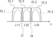
ここで、各々の光フィルタ11_1〜11_3は、互いに隣接する波長の光信号を各々通過させる各々の光フィルタの通過帯域の一部が互いに重畳するように構成されている。つまり、図2に示すように、光信号15_1(λ11)と光信号15_2(λ22)は互いに隣接しており、光フィルタ11_1の通過帯域13_1と光フィルタ11_2の通過帯域13_2は互いに隣接している。そして、光フィルタ11_1の通過帯域13_1の一部と光フィルタ11_2の通過帯域13_2の一部とが互いに重畳するように構成している(つまり、重畳領域17を設けている)。同様に、光信号15_2(λ22)と光信号15_3(λ33)は互いに隣接しており、光フィルタ11_2の通過帯域13_2と光フィルタ11_3の通過帯域13_3は互いに隣接している。そして、光フィルタ11_2の通過帯域13_2の一部と光フィルタ11_3の通過帯域13_3の一部とが互いに重畳するように構成している(つまり、重畳領域18を設けている)。 Here, each of the optical filters 11_1 to 11_3 is configured so that a part of the pass band of each optical filter that passes optical signals of wavelengths adjacent to each other overlap each other. That is, as shown in FIG. 2, the optical signal 15_1 (λ11) and the optical signal 15_2 (λ22) are adjacent to each other, and the pass band 13_1 of the optical filter 11_1 and the pass band 13_2 of the optical filter 11_2 are adjacent to each other. .. Then, a part of the pass band 13_1 of the optical filter 11_1 and a part of the pass band 13_2 of the optical filter 11_2 are configured to overlap each other (that is, a
周回性AWGを光デバイスとして用いた場合には、例えば、周回性AWGの入出力導波路の形状を調整し、各光フィルタに対応する通過帯域を広げることで、隣接するポート間で通過帯域を重畳させることができる。例えば、周回性AWGの各ポートの通過帯域は、周回性AWGの入力導波路と入力側のスラブ導波路の結合部と、出力側のスラブ導波路と出力導波の結合部の形状を調整することで広げることができる。 When the circumferential AWG is used as an optical device, for example, by adjusting the shape of the input / output waveguide of the orbital AWG and widening the pass band corresponding to each optical filter, the pass band can be increased between adjacent ports. Can be superimposed. For example, the passband of each port of the circumferential AWG adjusts the shape of the junction between the input waveguide and the slab waveguide on the input side and the coupling portion between the slab waveguide and the output waveguide on the output side. It can be expanded by.
図3の上図に示すように、光フィルタの形状は矩形ではなく、中心周波数と帯域幅に個体ばらつきがあるため、フィルタ数が増えると、受信端で見るフィルタの帯域幅は狭くなっていく(帯域狭窄)。このようなフィルタの特性により、光信号は伝送過程で両端が削られ信号成分が失われていき、最終的には受信端での信号誤りが増え、受信できなくなる。 As shown in the upper figure of FIG. 3, the shape of the optical filter is not rectangular, and there are individual variations in the center frequency and the bandwidth. Therefore, as the number of filters increases, the bandwidth of the filter seen at the receiving end becomes narrower. (Band narrowing). Due to the characteristics of such a filter, both ends of the optical signal are cut off in the transmission process and the signal component is lost, and finally the signal error at the receiving end increases and the optical signal cannot be received.
具体的に説明すると、図3の下図に示すように、光フィルタが多段連なると、通過帯域21_1〜21_3の帯域幅が元の帯域幅よりも狭くなり、帯域幅22_1〜22_3に示すようになる。結果として、各々の光信号λ11、λ22、λ33の両端が削られるため(削られた部分をハッチングで示す)、光信号λ11、λ22、λ33が受信できないレベルになる。 More specifically, as shown in the lower figure of FIG. 3, when the optical filters are connected in multiple stages, the bandwidth of the pass bands 21_1 to 21_3 becomes narrower than the original bandwidth, and the bandwidths 22_1 to 22_3 are shown. .. As a result, both ends of the respective optical signals λ11, λ22, and λ33 are cut (hatched portions are indicated by hatching), so that the optical signals λ11, λ22, and λ33 cannot be received.
このような問題を解決するために、本実施の形態にかかる光デバイス1では、各々の光フィルタ11_1〜11_3を構成する際に、互いに隣接する波長の光信号を各々通過させる各々の光フィルタの通過帯域の一部が互いに重畳するようにしている。つまり、図2に示すように、光フィルタ11_1の通過帯域13_1の一部と光フィルタ11_2の通過帯域13_2の一部とが重畳する重畳領域17を設けている。また、光フィルタ11_2の通過帯域13_2の一部と光フィルタ11_3の通過帯域13_3の一部とが重畳する重畳領域18を設けている。このような構成とすることで、光フィルタの帯域狭窄によって光信号λ11、λ22、λ33の両端が削られることを抑制することができ、受信できない光信号が発生することを抑制することができる。 In order to solve such a problem, in the
各々の光フィルタ11_1〜11_3の通過帯域に重畳領域17、18を設ける場合は、例えば、隣接する光フィルタ間の周波数間隔を維持しつつ、複数の光フィルタの各々の通過帯域幅を広げる。具体的に説明すると、図4Aに示すように、各々の光フィルタの周波数間隔を維持しつつ、光フィルタの通過帯域を、通過帯域21_1〜21_3(図3参照)から通過帯域13_1〜13_3になるように広げる。各々の光フィルタの周波数間隔は、光信号λ11、λ22、λ33のピーク間の周波数間隔に対応する。このようにすることで、各々の光フィルタ11_1〜11_3の通過帯域13_1〜13_3に重畳領域17、18を設けることができる。 When the overlapping
また、各々の光フィルタ11_1〜11_3の通過帯域13_1〜13_3の形状は任意の形状とすることができる。一例を挙げると、各々の光フィルタ11_1〜11_3として、スーパーガウシアン型の光フィルタを用いることができる。 Further, the shape of the pass band 13_1 to 13_3 of each optical filter 11_1 to 11_3 can be any shape. As an example, a super Gaussian type optical filter can be used as each of the optical filters 11_1 to 11_3.
他の手段としては、例えば波長選択スイッチWSSのスイッチ素子(LCOS:Liquid
crystal on silicon)の回折効率を調整することで通過帯域に重畳領域を設けることができる。As another means, for example, a switch element (LCOS: Liquid) of a wavelength selection switch WSS.
By adjusting the diffraction efficiency of crystal on silicon), a superposed region can be provided in the pass band.
本実施の形態では、LCOS素子で形成された波長選択スイッチWSSのスイッチ素子25を用いることで、通過帯域を広げるように調整することができる。 In the present embodiment, by using the
通過帯域に重畳領域を有する構成を備えない一般的な波長選択スイッチWSSを用いた場合には、波長選択スイッチWSSのスイッチ素子25から各ポートに入力される光信号の帯域は、互いに重畳しない。そのため、図4Bの左図に示すように、スイッチ素子25が各々異なる波長を備える光信号λ11、λ22、λ33をそれぞれ、ポートP1、P2、P3に入力されるようにスイッチングする際に、各光信号の帯域は、互いに重畳していない。よって、波長選択スイッチWSSのスイッチ素子は、各々の光信号λ11、λ22、λ33が互いに重畳しない状態でポートP1、P2、P3に入力されるようにスイッチングを行っている。 When a general wavelength selection switch WSS having no overlap region in the pass band is used, the bands of the optical signals input from the
すなわち、図4Bの左図に示すように、WSSの一般的な制御では、波長選択スイッチWSSのスイッチ素子25は、各々異なる波長を備える光信号λ11、λ22、λ33をそれぞれ、ポートP1、P2、P3に出力する。このとき、スイッチ素子25は各々の光信号λ11、λ22、λ33が互いに重畳しないようにスイッチングしている。 That is, as shown in the left figure of FIG. 4B, in the general control of WSS, the
これに対して本実施の形態にかかる光デバイスでは、波長選択スイッチWSSのスイッチ素子25がLCOS素子によって通過帯域の調整を行っている。スイッチ素子25のLCOS素子は、図4Bの右図に示すように、各々の光信号λ11、λ22、λ33の端部が互いに重畳するような通過帯域を有するように設定されている。 On the other hand, in the optical device according to the present embodiment, the
すなわち、本実施の形態の波長選択スイッチWSSのスイッチ素子25は、図4Bの右図に示すように、各々の光信号λ11、λ22、λ33の端部が互いに重畳するようにスイッチングする。波長選択スイッチWSSのスイッチ素子25は、各々の光信号λ11、λ22、λ33を各々のポートP1、P2、P3にスイッチングする際に、各々の光信号λ11、λ22、λ33の端部を互いに重畳させてスイッチングする。具体的には、スイッチ素子25は、光信号λ11がポートP1、及びポートP2の一部に出力されるようにスイッチングする。 That is, as shown in the right figure of FIG. 4B, the
また、スイッチ素子25は、光信号λ22がポートP1の一部、ポートP2、及びポートP3の一部に出力されるようにスイッチングする。また、スイッチ素子25は、光信号λ33がポートP3、及びポートP2の一部に出力されるようにスイッチングする。図4Bの右図において、スイッチ素子25が光信号をオーバーラップ制御している部分をハッチングで示している。また、各々の光信号λ11、λ22、λ33の強度Pを図4Bのグラフに示す。このような制御により、各々の光信号λ11、λ22、λ33の端部が互いに重畳するようにスイッチングすることができる。なお、図4Bでは、一例として1入力N出力(1×N)の波長選択スイッチWSSの場合を示したが、本実施の形態はN入力1出力(N×1)の波長選択スイッチWSSを用いても実現することができる。 Further, the
また、本実施の形態では、AWGの入出力導波路の形状を調整することで各々の光信号の通過帯域に重畳領域を設けてもよい。例えば、AWGのスラブ導波路と入出力導波路との結合部の形状を調整することで、各々の光信号の通過帯域に重畳領域を設けることができる。 Further, in the present embodiment, a superimposition region may be provided in the pass band of each optical signal by adjusting the shape of the input / output waveguide of the AWG. For example, by adjusting the shape of the coupling portion between the slab waveguide and the input / output waveguide of the AWG, a superimposition region can be provided in the pass band of each optical signal.
以上で説明した本実施の形態にかかる発明により、光フィルタの帯域狭窄によって光信号が削られることを抑制することが可能な光デバイスを提供することができる。 According to the invention according to the present embodiment described above, it is possible to provide an optical device capable of suppressing the reduction of an optical signal due to the narrowing of the band of the optical filter.
なお、上記では3入力1出力の光デバイス1(周回性AWG)を一例として示したが、本発明はこれに限定されることはなく、光デバイス1の入力ポートの数や出力ポートの数は任意に決定することができる。
<実施の形態2>
次に、本発明の実施の形態2について説明する。In the above, the optical device 1 (circular AWG) having 3 inputs and 1 output is shown as an example, but the present invention is not limited to this, and the number of input ports and the number of output ports of the
<
Next,
図5は、実施の形態2にかかる光デバイス2を説明するための図である。図5に示すように、本実施の形態にかかる光デバイス2は、複数のビームスプリッタBS_1〜BS_3と複数の周回性AWG_1〜AWG_3とを用いて構成されている。本実施の形態にかかる光デバイス2は、光通信ネットワークにおける光ノード、より具体的には光クロスコネクトノードに用いることができる。 FIG. 5 is a diagram for explaining the
図5に示すように、ビームスプリッタBS_1〜BS_3の各々の入力側は、3つの入力側方路IN_#1〜IN_#3と接続されている。ビームスプリッタBS_1〜BS_3から出力された光信号は、ビームスプリッタBS_1〜BS_3の後段に設けられている周回性AWG_1〜AWG_3に供給される。ビームスプリッタBS_1〜BS_3は1入力3出力(1×3)のビームスプリッタであり、周回性AWG_1〜AWG_3は3入力1出力(3×1)の周回性AWGである。周回性AWG_1〜AWG_3の各々の出力ポートは、出力側方路OUT_#1〜OUT_#3にそれぞれ接続されている。 As shown in FIG. 5, each input side of the beam splitters BS_1 to BS_3 is connected to three input sideways
ビームスプリッタBS_1〜BS_3の各々は、ビームスプリッタBS_1〜BS_3の各々に入力された各々の光信号を周回性AWG_1〜AWG_3の各々の入力ポートに出力する。具体的には、ビームスプリッタBS_1は入力側方路IN_#1から供給された光信号Ch11、Ch12、Ch13を、周回性AWG_1の入力ポートP1、周回性AWG_2の入力ポートP2、及び周回性AWG_3の入力ポートP3に供給する。同様に、ビームスプリッタBS_2は入力側方路IN_#2から供給された光信号Ch21、Ch22、Ch23を、周回性AWG_1の入力ポートP2、周回性AWG_2の入力ポートP3、及び周回性AWG_3の入力ポートP1に供給する。同様に、ビームスプリッタBS_3は入力側方路IN_#3から供給された光信号Ch31、Ch32、Ch33を、周回性AWG_1の入力ポートP3、周回性AWG_2の入力ポートP1、及び周回性AWG_3の入力ポートP2に供給する。 Each of the beam splitters BS_1 to BS_3 outputs each optical signal input to each of the beam splitters BS_1 to BS_3 to each input port of the circumferential AWG_1 to AWG_3. Specifically, the beam splitter BS_1 uses the optical signals Ch11, Ch12, and Ch13 supplied from the input sideways
各々の周回性AWG_1〜AWG_3は、各々の入力ポートP1〜P3に入力された各々の光信号をフィルタリングして出力側方路に出力する。具体的には、周回性AWG_1は、入力ポートP1〜P3に入力された光信号のうち光信号Ch11、Ch32、Ch23を出力側方路OUT_#1に出力する。また、周回性AWG_2は、入力ポートP1〜P3に入力された光信号のうち光信号Ch21、Ch12、Ch33を出力側方路OUT_#2に出力する。また、周回性AWG_3は、入力ポートP1〜P3に入力された光信号のうち光信号Ch31、Ch22、Ch13を出力側方路OUT_#3に出力する。 Each orbiting AWG_1 to AWG_3 filters the respective optical signals input to the respective input ports P1 to P3 and outputs them to the output sideways. Specifically, the circumferential AWG_1 outputs the optical signals Ch11, Ch32, and Ch23 among the optical signals input to the input ports P1 to P3 to the output side
ここで、入力側方路IN_#1を通る各々の光信号Ch11、Ch12、Ch13は、各々異なる周波数帯域の光信号である。入力側方路IN_#2を通る各々の光信号Ch21、Ch22、Ch23、及び入力側方路IN_#3を通る各々の光信号Ch31、Ch32、Ch33についても同様である。 Here, the respective optical signals Ch11, Ch12, and Ch13 passing through the input side
一方、入力側方路IN_#1の光信号Ch11、入力側方路IN_#2の光信号Ch21、及び入力側方路IN_#3の光信号Ch31は同一の周波数帯域の光信号である。同様に、入力側方路IN_#1の光信号Ch12、入力側方路IN_#2の光信号Ch22、及び入力側方路IN_#3の光信号Ch32は同一の周波数帯域の光信号である。同様に、入力側方路IN_#1の光信号Ch13、入力側方路IN_#2の光信号Ch23、及び入力側方路IN_#3の光信号Ch33は同一の周波数帯域の光信号である。このため、WDM通信を実現するためには、これらの光信号が同一の出力側方路に出力されないようにする必要がある。 On the other hand, the optical signal Ch11 of the input side
また、本実施の形態にかかる光デバイス2では、各々の光信号(Ch11、Ch12、Ch13、・・・Ch33)はチャネル単位でルーティングされる。また、1つのチャネルの帯域内に複数の波長多重信号を割り当て可能に構成されている。 Further, in the
図6は、本実施の形態にかかる光デバイス2で用いられているチャネルの帯域幅を説明するための図である。図6に示すように、本実施の形態にかかる光デバイス2では、1つのチャネル帯域31の中に複数の波長多重信号(光信号)32を割り当てることができる。図6では、一例として、各々のチャネルCh11、Ch12、Ch13の帯域幅を150GHzとし、チャネルCh11の中に50GHzの帯域幅の光信号を3つ割り当てた場合を示している。また、チャネルCh12の中に37.5GHzの帯域幅の光信号を4つ割り当てた場合を示している。また、チャネルCh13の中に100GHzの帯域幅の光信号と50GHzの帯域幅の光信号とを割り当てた場合を示している。なお、図6に示した例は一例であり、各々のチャネル帯域31の帯域幅は任意に決定することができる。また、各々のチャネルの帯域内に割り当てる光信号32の帯域幅および数は任意に決定することができる。 FIG. 6 is a diagram for explaining the bandwidth of the channel used in the
そして、本実施の形態にかかる光デバイス2では、周回性AWG_1〜AWG_3の各々の入力ポートP1〜P3の通過帯域幅(つまり、光フィルタの帯域幅)を、チャネル(Ch11、Ch12、Ch13、・・・Ch33)の帯域幅に対応するようにしている。換言すると、周回性AWG_1〜AWG_3の各々の入力ポートP1〜P3の通過帯域幅をチャネルの帯域幅まで広げることで、所定の帯域幅を持った光信号(つまり、チャネルCh11、Ch12、Ch13、・・・Ch33)を各々フィルタリングすることができる。例えば、チャネルCh11をチャネル単位でフィルタリングすることで、50GHzの帯域幅の光信号32を3つ同一方向にフィルタリングすることができる。 Then, in the
例えば、周回性AWG_1の入力ポートP1には光信号Ch11、Ch12、Ch13が供給され、入力ポートP2には光信号Ch21、Ch22、Ch23が供給され、入力ポートP3には光信号Ch31、Ch32、Ch33が供給される。このとき、各々の入力ポートP1〜P3の通過帯域幅を150GHzとすることで、1チャネル当たりの帯域幅が150GHzの光信号を通過させることができる。 For example, optical signals Ch11, Ch12, and Ch13 are supplied to the input port P1 of the circumferential AWG_1, optical signals Ch21, Ch22, and Ch23 are supplied to the input port P2, and optical signals Ch31, Ch32, and Ch33 are supplied to the input port P3. Is supplied. At this time, by setting the pass bandwidth of each of the input ports P1 to P3 to 150 GHz, an optical signal having a bandwidth of 150 GHz per channel can be passed.
例えば、周回性AWG_1の入力ポートP1の通過帯域と中心周波数とを光信号Ch11の周波数帯域と中心周波数とに合わせることで、入力ポートP1に供給された光信号Ch11、Ch12、Ch13のうち光信号Ch11のみを通過させることができる。すなわち、入力ポートP1の通過帯域、すなわち、光フィルタの通過帯域と中心周波数とを光信号Ch11の周波数帯域と中心周波数とに合わせることで、光信号Ch12、Ch13を除去することができる。 For example, by matching the pass band and the center frequency of the input port P1 of the circumferential AWG_1 with the frequency band and the center frequency of the optical signal Ch11, the optical signal among the optical signals Ch11, Ch12, and Ch13 supplied to the input port P1 Only Ch11 can be passed. That is, the optical signals Ch12 and Ch13 can be removed by matching the pass band of the input port P1, that is, the pass band and the center frequency of the optical filter with the frequency band and the center frequency of the optical signal Ch11.
同様に、周回性AWG_1の入力ポートP2の通過帯域と中心周波数とを光信号Ch23の周波数帯域と中心周波数とに合わせることで、入力ポートP2に供給された光信号Ch21、Ch22、Ch23のうち光信号Ch23のみを通過させることができる。 Similarly, by matching the pass band and the center frequency of the input port P2 of the circumferential AWG_1 with the frequency band and the center frequency of the optical signal Ch23, the optical signals Ch21, Ch22, and Ch23 supplied to the input port P2 are optical. Only the signal Ch23 can be passed.
同様に、周回性AWG_1の入力ポートP3の通過帯域と中心周波数とを光信号Ch32の周波数帯域と中心周波数とに合わせることで、入力ポートP3に供給された光信号Ch31、Ch32、Ch33のうち光信号Ch32のみを通過させることができる。 Similarly, by matching the pass band and the center frequency of the input port P3 of the circumferential AWG_1 with the frequency band and the center frequency of the optical signal Ch32, the optical signals Ch31, Ch32, and Ch33 supplied to the input port P3 are optical. Only the signal Ch32 can be passed.
例えば、各々の周回性AWG_1〜AWG_3の各々の入力ポートP1〜P3の通過帯域幅は、複数の波長多重信号の隣接周波数間隔のm倍(mは2以上の正の実数)としてもよい。例えば、波長多重信号の隣接周波数間隔を37.5GHz、m=4とした場合、入力ポートP1〜P3の通過帯域幅は150GHzとなる(図6のCh12参照)。この場合は、1つの光信号で100Gbpsの容量の通信を行うとすると、1つのチャネルの中に37.5GHzの帯域幅の光信号を4つ割り当てることができるので、400Gbpsの容量の通信を実現することができる。 For example, the pass bandwidth of each input port P1 to P3 of each orbiting AWG_1 to AWG_3 may be m times (m is a positive real number of 2 or more) of adjacent frequency intervals of a plurality of wavelength division multiplexing signals. For example, when the adjacent frequency interval of the wavelength division multiplexing signal is 37.5 GHz and m = 4, the pass bandwidth of the input ports P1 to P3 is 150 GHz (see Ch12 in FIG. 6). In this case, if one optical signal is used for communication with a capacity of 100 Gbps, four optical signals with a bandwidth of 37.5 GHz can be assigned to one channel, so that communication with a capacity of 400 Gbps can be realized. can do.
また、例えば、波長多重信号の隣接周波数間隔を50GHz、m=3とした場合、入力ポートP1〜P3の通過帯域幅は150GHzとなる(図6のCh11参照)。この場合は、1つの光信号で100Gbpsの容量の通信を行うとすると、1つのチャネルの中に50GHzの帯域幅の光信号を3つ割り当てることができるので、300Gbpsの容量の通信を実現することができる。また、例えば、波長多重信号の隣接周波数間隔を75GHz、m=2とした場合も、入力ポートP1〜P3の通過帯域幅は150GHzとなる。また、上記の例はあくまでも一例であり、当該信号の変調方式、容量から最適な信号間隔、AWGの追加帯域幅(信号間隔のm倍)が決定される。 Further, for example, when the adjacent frequency interval of the wavelength division multiplexing signal is 50 GHz and m = 3, the pass bandwidth of the input ports P1 to P3 is 150 GHz (see Ch11 in FIG. 6). In this case, assuming that one optical signal is used for communication with a capacity of 100 Gbps, three optical signals with a bandwidth of 50 GHz can be assigned to one channel, so that communication with a capacity of 300 Gbps can be realized. Can be done. Further, for example, even when the adjacent frequency interval of the wavelength division multiplexing signal is 75 GHz and m = 2, the pass bandwidth of the input ports P1 to P3 is 150 GHz. Further, the above example is only an example, and the optimum signal interval and the additional bandwidth of the AWG (m times the signal interval) are determined from the modulation method and capacitance of the signal.
上記で説明したように、本実施の形態にかかる光デバイス2では、1つのチャネルの帯域内に複数の波長多重信号を割り当て可能に構成されている。ここで、1つのチャネルの帯域内に割り当てられる複数の波長多重信号の数や帯域幅は任意に設定することができる。 As described above, the
つまり、1つのチャネルに1つの光信号しか割り当てられない場合は、チャネルと光信号とが一対一に対応している。そのため入力側方路IN_#1〜IN_#3に供給される各々の光信号と、出力側方路OUT_#1〜OUT_#3から出力される各々の光信号との関係は一意に決定されていた。換言すると、入力側方路IN_#1〜IN_#3に供給される各々の光信号と、出力側方路OUT_#1〜OUT_#3から出力される各々の光信号との関係は固定されていた。そのため、光通信ネットワークにおける運用の柔軟性に欠けるという問題があった。 That is, when only one optical signal is assigned to one channel, there is a one-to-one correspondence between the channel and the optical signal. Therefore, the relationship between each optical signal supplied to the input sideways
これに対して本実施の形態にかかる光デバイス2では、1つのチャネルの帯域内に複数の波長多重信号を割り当て可能に構成している。更に、周回性AWGがチャネル単位で光信号をフィルタリングすることができるように、周回性AWGの各々の入力ポートの通過帯域幅(つまり、各々の入力ポートに対応した各々の光フィルタの通過帯域幅)を広げている。よって、各々のチャネル内に割り当てられる複数の波長多重信号の数や帯域幅を任意に設定することができるので、伝送する光信号に柔軟性を持たせることができる。つまり、図6に示すように、1チャネル内に割り当てる光信号の数を変えたり(チャネルCh11、Ch12参照)、1チャネル内に各々異なる帯域幅を有する光信号を割り当てたりすることができる(チャネルCh13参照)。そのため、伝送する光信号に柔軟性を持たせることができる。 On the other hand, the
また、本実施の形態にかかる光デバイス2では、周回性AWG_1〜AWG_3を用いているので、同一の周波数帯域の信号が同一の出力側方路に出力されることを回避することができる。 Further, since the
ところで、本実施の形態にかかる光デバイス2では、1つのチャネルの帯域内に複数の波長多重信号を割り当てている。光信号を高密度(高収容率)で伝送するためには、図7の上図に示すように、光フィルタの通過帯域41の帯域幅と4つの光信号42の帯域幅(つまり、1チャネル当たりの帯域幅)との間に差がないほうが好ましい。例えば、図7の上図に示す場合は、1つの光信号42の帯域幅が37.5GHzでこの光信号42の数が4つであるので、4つの光信号42の帯域幅(1チャネル当たりの帯域幅)は37.5GHz×4=150GHzとなる。この場合は、光フィルタの通過帯域41も150GHzとすることで、光信号を高密度に伝送することができる。 By the way, in the
しかしながら、光フィルタの形状は矩形ではなく、中心周波数と帯域幅に個体ばらつきがあるため、フィルタ数が増えると、受信端で見るフィルタの帯域幅は狭くなっていく(帯域狭窄)。このようなフィルタの特性により、光信号は伝送過程で両端が削られ信号成分が失われていき、最終的には受信端での信号誤りが増え、受信できなくなる。具体的に説明すると、図7の下図に示すように、光フィルタが多段連なると、通過帯域41の帯域幅が元の帯域幅よりも狭くなり、帯域幅43に示すようになる。結果として、4つある光信号42のうちの両端の信号が削られるため(削られた部分をハッチングで示す)、両端の信号が受信できないレベルになる場合がある。 However, since the shape of the optical filter is not rectangular and there are individual variations in the center frequency and bandwidth, the bandwidth of the filter seen at the receiving end becomes narrower as the number of filters increases (bandwidth narrowing). Due to the characteristics of such a filter, both ends of the optical signal are cut off in the transmission process and the signal component is lost, and finally the signal error at the receiving end increases and the optical signal cannot be received. More specifically, as shown in the lower figure of FIG. 7, when the optical filters are connected in multiple stages, the bandwidth of the
このような現象を抑制するために、光信号と光フィルタ帯域の両端との間に空白エリア(つまり、ガードバンド)を設けることも考えられる。しかし、この場合は、ガードバンドを設けた分だけ光信号の収容率が低下してしまうという問題がある。 In order to suppress such a phenomenon, it is conceivable to provide a blank area (that is, a guard band) between the optical signal and both ends of the optical filter band. However, in this case, there is a problem that the accommodation rate of the optical signal is lowered by the amount of the guard band provided.
このような問題を解決するために、本実施の形態にかかる光デバイス2では、互いに隣接するチャネルの光信号を各々通過させる各々の光フィルタの通過帯域の一部が互いに重畳するように各々の光フィルタを構成している。具体的に説明すると、図5に示した周回性AWG_1のポートP1の光フィルタの通過帯域の一部とポートP2の光フィルタの通過帯域の一部とが、図8に示す通過帯域51_1、51_2のように互いに重畳するように構成している。すなわち、周回性AWG_1のポートP1とポートP2の光フィルタの通過帯域に重畳領域55が設けられている。このとき、周回性AWG_1のポートP1の光フィルタの通過帯域は、チャネルCh11の波長帯域に対応している。また、周回性AWG_1のポートP2の光フィルタの通過帯域は、チャネルCh32の波長帯域に対応している。 In order to solve such a problem, in the
周回性AWGの光フィルタの通過帯域は、例えば、周回性AWGの入出力導波路の形状を調整することで可変とすることができる。各光フィルタに対応する通過帯域を広げることで、隣接するポートに対応する光フィルタ間で通過帯域を重畳させることができる。例えば、周回性AWGの各ポートに対応する通過帯域は、周回性AWGの入力導波路と入力側のスラブ導波路の結合部と、出力側のスラブ導波路と出力導波の結合部の形状を調整することで広げることができる。 The pass band of the circumferential AWG optical filter can be made variable by, for example, adjusting the shape of the input / output waveguide of the circumferential AWG. By expanding the pass band corresponding to each optical filter, the pass band can be superimposed between the optical filters corresponding to the adjacent ports. For example, the pass band corresponding to each port of the circumferential AWG is the shape of the coupling part of the input waveguide and the slab waveguide on the input side of the circumferential AWG and the coupling part of the slab waveguide and the output waveguide on the output side. It can be expanded by adjusting.
また、図5に示した周回性AWG_1のポートP2の光フィルタの通過帯域の一部とポートP3の光フィルタの通過帯域の一部とが、図8に示す通過帯域51_2、51_3のように互いに重畳するように構成している。すなわち、周回性AWG_1のポートP2とポートP3の光フィルタの通過帯域に重畳領域56を設けられている。このとき、周回性AWG_1のポートP2の光フィルタの通過帯域は、チャネルCh32の波長帯域に対応している。また、周回性AWG_1のポートP3の光フィルタの通過帯域は、チャネルCh23の波長帯域に対応している。 Further, a part of the pass band of the optical filter of the port P2 of the cyclic AWG_1 shown in FIG. 5 and a part of the pass band of the optical filter of the port P3 are mutual as shown in the pass bands 51_2 and 51_3 of FIG. It is configured to overlap. That is, the
例えば、互いに隣接するチャネルに対応した各々の光フィルタの周波数間隔を維持しつつ、各々の光フィルタの通過帯域を広げることで、互いに隣接するチャネルに対応した光フィルタの通過帯域の一部を互いに重畳させることができる。具体例を用いて説明すると、図8に示すように、各々のチャネルの周波数間隔54を150GHzとしたまま、各々のチャネルに対応した光フィルタの通過帯域51_1〜51_3の幅を150GHzから162.5GHzに広げる。 For example, by widening the pass band of each optical filter while maintaining the frequency interval of each optical filter corresponding to the adjacent channels, a part of the pass band of the optical filters corresponding to the adjacent channels can be partially divided into each other. It can be superimposed. To explain using a specific example, as shown in FIG. 8, the width of the pass band 51_1 to 51_3 of the optical filter corresponding to each channel is changed from 150 GHz to 162.5 GHz while the
このようにすることで、通過帯域51_1の一部と通過帯域51_2の一部とを重畳させることができる。この場合は、通過帯域51_1と通過帯域51_2とが重畳する重畳領域55の幅は12.5GHzとなる。同様に、通過帯域51_2の一部と通過帯域51_3の一部とを重畳させることができる。この場合も、通過帯域51_2と通過帯域51_3とが重畳する重畳領域56の幅は12.5GHzとなる。 By doing so, a part of the pass band 51_1 and a part of the pass band 51-2 can be superimposed. In this case, the width of the superposed
上記で説明したように、本実施の形態にかかる光デバイス2では、互いに隣接するチャネルの光信号を各々通過させる各々の光フィルタの通過帯域の一部が互いに重畳するように各々の光フィルタを構成している。よって、光信号の帯域狭窄によって伝送過程で光信号の両端が削られることを抑制でき、受信できない光信号が発生することを抑制できる。したがって、伝送特性の劣化を抑制することができる。 As described above, in the
一方で、隣接するチャネルの光フィルタの通過帯域の一部を重畳させると、隣接する他のチャネルの光信号が漏れ込みクロストークが発生する。しかし、フィルタ帯域狭窄とクロストークとを比較して光信号の劣化が最小となるようにフィルタのオーバーラップ幅を最適化することにより、最良の伝送特性を得ることができる。 On the other hand, when a part of the pass band of the optical filter of the adjacent channel is superimposed, the optical signal of the other adjacent channel leaks and crosstalk occurs. However, the best transmission characteristics can be obtained by optimizing the overlap width of the filters so that the deterioration of the optical signal is minimized by comparing the filter band narrowing and the crosstalk.
なお、図5に示した光デバイス2では、入力側方路および出力側方路の数がそれぞれ3つである場合を例として示した。しかし本実施の形態にかかる光デバイス2では、入力側方路および出力側方路の数はこれ以外であってもよい。つまり、n個の入力側方路IN_#1〜IN_#nとn個の出力側方路OUT_#1〜OUT_#nとを有する構成の場合は、入力側方路IN_#1〜IN_#nにそれぞれ接続されたn個のビームスプリッタBS_1〜BS_n(1入力n出力のビームスプリッタ)を設ける。nは、2以上の自然数である。 In the
また、n個のビームスプリッタBS_1〜BS_nの後段にn個の周回性AWG_1〜AWG_n(n入力1出力の周回性AWG)を設ける。n個のビームスプリッタBS_1〜BS_nの各々は、n個のビームスプリッタBS_1〜BS_nの各々に入力された各々の光信号をn個の周回性AWG_1〜AWG_nの各々の入力ポートに出力する。n個の周回性AWG_1〜AWG_nの各々は、各々の入力ポートに入力された各々の光信号をフィルタリングして出力側方路に出力する。これにより、出力側方路OUT_#1〜OUT_#nにはルーティング後の光信号が出力される。 Further, n orbital AWG_1 to AWG_n (n-input, 1-output orbital AWG) are provided after the n beam splitters BS_1 to BS_n. Each of the n beam splitters BS_1 to BS_n outputs each optical signal input to each of the n beam splitters BS_1 to BS_n to the respective input ports of the n circumferential AWG_1 to AWG_n. Each of the n orbiting AWG_1 to AWG_n filters the respective optical signal input to each input port and outputs it to the output side path. As a result, the optical signal after routing is output to the output sideways
以上で説明した本実施の形態にかかる発明により、光フィルタの帯域狭窄によって光信号が削られることを抑制することが可能な光デバイスを提供することができる。 According to the invention according to the present embodiment described above, it is possible to provide an optical device capable of suppressing the reduction of an optical signal due to the narrowing of the band of the optical filter.
上記の実施形態の一部又は全部は、以下の付記のようにも記載されうるが、以下には限られない。 Some or all of the above embodiments may also be described, but not limited to:
(付記1)
波長が異なる複数の光信号の中から所定の帯域の光信号をフィルタリングする光フィルタを複数備え、
前記複数の光フィルタは、互いに隣接する波長の光信号を各々通過させる各々の光フィルタの通過帯域の一部が互いに重畳するように構成されている、
光デバイス。(Appendix 1)
It is equipped with a plurality of optical filters that filter optical signals in a predetermined band from a plurality of optical signals having different wavelengths.
The plurality of optical filters are configured such that a part of the pass band of each optical filter that passes optical signals having wavelengths adjacent to each other overlap each other.
Optical device.
(付記2)
隣接する光フィルタ間の周波数間隔を維持しつつ前記複数の光フィルタの各々の通過帯域幅を広げることで、前記隣接する光フィルタの各々の通過帯域の一部を互いに重畳させる、付記1に記載の光デバイス。(Appendix 2)
The following is described in
(付記3)
前記複数の光フィルタは、スーパーガウシアン型の光フィルタまたはスーパーガウシアン関数で近似可能な光フィルタである、付記1または2に記載の光デバイス。(Appendix 3)
The optical device according to
(付記4)
前記複数の光フィルタの1つの当たりの通過帯域幅は、複数の光信号を同時に通過させることができる帯域幅である、付記1乃至3のいずれか一項に記載の光デバイス。(Appendix 4)
The optical device according to any one of
(付記5)
前記光デバイスは、前記各々の光信号をフィルタリングする周回性AWGであり、
前記各々の光信号はチャネル単位でフィルタリングされ、
前記チャネルは、当該チャネルの帯域内に複数の光信号を割り当て可能に構成されており、
前記周回性AWGの前記光フィルタの1つの当たりの通過帯域幅は前記チャネルの帯域幅に対応している、
付記1乃至4のいずれか一項に記載の光デバイス。(Appendix 5)
The optical device is a circular AWG that filters each of the optical signals.
Each of the optical signals is filtered on a channel-by-channel basis.
The channel is configured so that a plurality of optical signals can be assigned within the band of the channel.
The passband per one of the optical filters of the circumferential AWG corresponds to the bandwidth of the channel.
The optical device according to any one of
(付記6)
前記周回性AWGの前記光フィルタの1つ当たりの通過帯域幅は、前記複数の光信号の隣接周波数間隔のm倍(mは2以上の正の実数)である、付記5に記載の光デバイス。(Appendix 6)
The optical device according to Appendix 5, wherein the pass bandwidth per one of the optical filters of the circumferential AWG is m times (m is a positive real number of 2 or more) of the adjacent frequency intervals of the plurality of optical signals. ..
(付記7)
前記周回性AWGの前記各々の光フィルタの通過帯域幅は150GHzで、中心周波数間隔は150GHzである、付記6に記載の光デバイス。(Appendix 7)
The optical device according to Appendix 6, wherein the passband of each of the circumferential AWG's optical filters is 150 GHz and the center frequency interval is 150 GHz.
(付記8)
前記隣接周波数間隔は37.5GHzであり、前記mの値はm=4である、付記7に記載の光デバイス。(Appendix 8)
The optical device according to Appendix 7, wherein the adjacent frequency interval is 37.5 GHz, and the value of m is m = 4.
(付記9)
前記隣接周波数間隔は50GHzであり、前記mの値はm=3である、付記7に記載の光デバイス。(Appendix 9)
The optical device according to Appendix 7, wherein the adjacent frequency interval is 50 GHz and the value of m is m = 3.
(付記10)
前記隣接周波数間隔は75GHzであり、前記mの値はm=2である、付記7に記載の光デバイス。(Appendix 10)
The optical device according to Appendix 7, wherein the adjacent frequency interval is 75 GHz, and the value of m is m = 2.
(付記11)
前記光デバイスは通過帯域が可変可能な波長選択スイッチである、付記1乃至3のいずれか一項に記載の光デバイス。(Appendix 11)
The optical device according to any one of
(付記12)
前記光デバイスはAWGである、付記1乃至3のいずれか一項に記載の光デバイス。(Appendix 12)
The optical device according to any one of
(付記13)
互いに隣接する波長の光信号を各々通過させる通過帯域の一部が互いに重畳している複数の光フィルタに、波長多重化された光信号を入力し、
波長が異なる複数の前記光信号の中から所定の帯域の光信号をフィルタリングする、光信号の処理方法。(Appendix 13)
Wavelength-multiplexed optical signals are input to a plurality of optical filters in which part of the pass band that passes optical signals of adjacent wavelengths are superimposed on each other.
A method for processing an optical signal, which filters an optical signal in a predetermined band from a plurality of the optical signals having different wavelengths.
(付記14)
隣接する前記光フィルタ間の周波数間隔を維持しつつ前記複数の光フィルタの各々の通過帯域幅を広げることで、前記隣接する光フィルタの各々の通過帯域の一部を互いに重畳させる、付記13に記載の光信号の処理方法。(Appendix 14)
Note 13: By expanding the pass bandwidth of each of the plurality of optical filters while maintaining the frequency interval between the adjacent optical filters, a part of the pass band of each of the adjacent optical filters is superimposed on each other. The method for processing an optical signal described.
(付記15)
前記複数の光フィルタの1つの当たりの通過帯域幅は、複数の光信号を同時に通過させることができる帯域幅である、付記13または14に記載の光信号の処理方法。(Appendix 15)
The optical signal processing method according to
(付記16)
前記光フィルタは、前記各々の光信号をフィルタリングする際の通過帯域幅がチャネルの帯域内に複数の光信号が割り当てられている前記チャネルの帯域幅に対応するように設定され、
前記各々の光信号を前記チャネル単位でフィルタリングする、付記13乃至15に記載の光信号の処理方法。(Appendix 16)
The optical filter is set so that the pass band when filtering each of the optical signals corresponds to the bandwidth of the channel to which a plurality of optical signals are allocated within the band of the channel.
The optical signal processing method according to
以上、上述した実施形態を模範的な例として本発明を説明した。しかしながら、本発明は、上述した実施形態には限定されない。即ち、本発明は、本発明のスコープ内において、当業者が理解し得る様々な態様を適用することができる。 The present invention has been described above using the above-described embodiment as a model example. However, the present invention is not limited to the above-described embodiments. That is, the present invention can apply various aspects that can be understood by those skilled in the art within the scope of the present invention.
この出願は、2016年2月29日に出願された日本出願特願2016−38163を基礎とする優先権を主張し、その開示の全てをここに取り込む。 This application claims priority on the basis of Japanese application Japanese Patent Application No. 2016-38163 filed on February 29, 2016, the entire disclosure of which is incorporated herein by reference.
1、2 光デバイス
11_1〜11_3 光フィルタ
12 合波部
13_1〜13_3 通過帯域
15_1〜15_3 光信号
17、18 重畳領域
21_1〜21_3 通過帯域
22_1〜22_3 帯域幅
31 通過帯域
32 光信号
41 通過帯域
42 光信号
43 帯域幅
51_1〜51_3 通過帯域
52 光信号
54 周波数間隔
55、56 重畳領域1, 2 Optical device 11_1 to 11_3
Claims (6)
前記複数の光フィルタは、互いに隣接する波長の光信号を各々通過させる各々の光フィルタとの間の周波数間隔を維持しつつ通過帯域幅を広げることで通過帯域の一部が互いに重畳するように構成されており、
前記通過帯域の重畳の量は、各々の前記光フィルタの帯域狭窄による前記光フィルタを通過する光信号のレベル低下と各々の前記光フィルタのクロストークによる漏れ込みとを比較して各々の前記光フィルタを通過する光信号の信号電力対雑音電力比の劣化が最小となるように設定され、
前記複数の光フィルタの1つ当たりの通過帯域幅は、複数の光信号を同時に通過させることができる帯域幅である、
光デバイス。 It is equipped with a plurality of optical filters that filter optical signals in a predetermined band from a plurality of optical signals having different wavelengths.
The plurality of optical filters are such that a part of the pass band overlaps with each other by widening the pass bandwidth while maintaining the frequency interval between each optical filter that passes optical signals of wavelengths adjacent to each other. It is composed and
The amount of superimposition of the pass band is determined by comparing the level decrease of the optical signal passing through the optical filter due to the band narrowing of each optical filter with the leakage due to the crosstalk of each optical filter. It is set to minimize the deterioration of the signal power to noise power ratio of the optical signal passing through the filter .
The pass bandwidth per one of the plurality of optical filters is a bandwidth capable of passing a plurality of optical signals at the same time.
Optical device.
前記各々の光信号はチャネル単位でフィルタリングされ、
前記チャネルは、当該チャネルの帯域内に複数の光信号を割り当て可能に構成されており、
前記周回性AWGの前記光フィルタの1つの当たりの通過帯域幅は前記チャネルの帯域幅に対応している、
請求項1又は2に記載の光デバイス。 The optical device is a circular AWG that filters each of the optical signals.
Each of the optical signals is filtered on a channel-by-channel basis.
The channel is configured so that a plurality of optical signals can be assigned within the band of the channel.
The passband per one of the optical filters of the circumferential AWG corresponds to the bandwidth of the channel.
The optical device according to claim 1 or 2 .
波長が異なる複数の前記光信号の中から所定の帯域の光信号をフィルタリングする、光信号の処理方法であって、
隣接する前記光フィルタ間の周波数間隔を維持しつつ前記複数の光フィルタの各々の通過帯域幅を広げることで、前記隣接する光フィルタの各々の通過帯域の一部を互いに重畳させ、
前記通過帯域の重畳の量は、各々の前記光フィルタの帯域狭窄による前記光フィルタを通過する光信号のレベル低下と各々の前記光フィルタのクロストークによる漏れ込みとを比較して各々の前記光フィルタを通過する光信号の信号電力対雑音電力比の劣化が最小となるように設定され、
前記複数の光フィルタの1つの当たりの通過帯域幅は、複数の光信号を同時に通過させることができる帯域幅である、
光信号の処理方法。 Wavelength-multiplexed optical signals are input to a plurality of optical filters in which part of the pass band that passes optical signals of adjacent wavelengths are superimposed on each other.
A method for processing an optical signal, which filters an optical signal in a predetermined band from a plurality of the optical signals having different wavelengths.
By widening the pass bandwidth of each of the plurality of optical filters while maintaining the frequency interval between the adjacent optical filters, a part of the pass band of each of the adjacent optical filters is superimposed on each other.
The amount of superimposition of the pass band is determined by comparing the level decrease of the optical signal passing through the optical filter due to the band narrowing of each optical filter with the leakage due to the crosstalk of each optical filter. It is set to minimize the deterioration of the signal power to noise power ratio of the optical signal passing through the filter .
The pass bandwidth per one of the plurality of optical filters is a bandwidth capable of passing a plurality of optical signals at the same time.
Optical signal processing method.
前記各々の光信号を前記チャネル単位でフィルタリングする、請求項5に記載の光信号の処理方法。 The optical filter is set so that the pass band when filtering each of the optical signals corresponds to the bandwidth of the channel to which a plurality of optical signals are allocated within the band of the channel.
The optical signal processing method according to claim 5, wherein each of the optical signals is filtered for each channel.
Applications Claiming Priority (3)
| Application Number | Priority Date | Filing Date | Title |
|---|---|---|---|
| JP2016038163 | 2016-02-29 | ||
| JP2016038163 | 2016-02-29 | ||
| PCT/JP2017/006394 WO2017150278A1 (en) | 2016-02-29 | 2017-02-21 | Optical device |
Publications (2)
| Publication Number | Publication Date |
|---|---|
| JPWO2017150278A1 JPWO2017150278A1 (en) | 2018-12-06 |
| JP6763424B2 true JP6763424B2 (en) | 2020-09-30 |
Family
ID=59742805
Family Applications (1)
| Application Number | Title | Priority Date | Filing Date |
|---|---|---|---|
| JP2018503058A Active JP6763424B2 (en) | 2016-02-29 | 2017-02-21 | Optical device |
Country Status (5)
| Country | Link |
|---|---|
| US (1) | US10539741B2 (en) |
| EP (1) | EP3425434A4 (en) |
| JP (1) | JP6763424B2 (en) |
| CN (1) | CN109313309B (en) |
| WO (1) | WO2017150278A1 (en) |
Families Citing this family (6)
| Publication number | Priority date | Publication date | Assignee | Title |
|---|---|---|---|---|
| CN109075885B (en) * | 2016-02-29 | 2020-09-18 | 日本电气株式会社 | Optical transmission device |
| JP6988296B2 (en) * | 2017-09-14 | 2022-01-05 | 富士通株式会社 | Transmission equipment and signal monitoring method |
| US10701465B2 (en) * | 2017-11-10 | 2020-06-30 | Huawei Technologies Co., Ltd. | Wide passband wavelength selective switch |
| CN109067472B (en) * | 2018-08-23 | 2021-09-07 | 东南大学 | Multicolor optical signal receiving method based on overlapping covering optical filter set |
| EP3849114B1 (en) | 2018-09-07 | 2024-04-10 | NEC Corporation | Optical transmission device, optical communication system, and optical signal transmission method |
| JP7360024B2 (en) * | 2019-08-30 | 2023-10-12 | 富士通株式会社 | network system |
Family Cites Families (17)
| Publication number | Priority date | Publication date | Assignee | Title |
|---|---|---|---|---|
| JPH09321701A (en) * | 1996-05-31 | 1997-12-12 | Fujitsu Ltd | Optical communication system and optical amplifier |
| EP0936483A3 (en) * | 1998-02-10 | 1999-09-22 | Lucent Technologies Inc. | Optical router with coherent connecting paths |
| EP1030480A3 (en) | 1999-02-19 | 2002-06-12 | JDS Uniphase Inc. | Configurable optical circuit |
| JP4647074B2 (en) * | 2000-10-04 | 2011-03-09 | 富士通株式会社 | WDM optical communication system |
| JP4622168B2 (en) * | 2001-06-22 | 2011-02-02 | 住友電気工業株式会社 | Wavelength multiplexed signal light monitoring device, monitoring method, and optical transmission system |
| US20030016911A1 (en) * | 2001-07-19 | 2003-01-23 | Samad Talebpour | Random access optical add/drop switch |
| JP4540289B2 (en) | 2002-06-28 | 2010-09-08 | 富士通株式会社 | Wavelength division multiplexing optical transmission system and wavelength division multiplexing optical transmission method |
| JP5691255B2 (en) * | 2010-06-22 | 2015-04-01 | 富士通株式会社 | OSNR measuring apparatus and optical communication system |
| JP5466657B2 (en) | 2011-02-18 | 2014-04-09 | 日本電信電話株式会社 | Wavelength tuning system and method |
| CN102695101B (en) * | 2011-03-21 | 2015-11-18 | 苏州海光芯创光电科技有限公司 | EPON on a kind of wavelength division multiplexing |
| US9160455B2 (en) * | 2011-07-14 | 2015-10-13 | Applied Optoelectronics, Inc. | External cavity laser array system and WDM optical system including same |
| GB201119922D0 (en) * | 2011-11-18 | 2012-01-04 | Cambridge Entpr Ltd | Optical signal transmission systems |
| JP5962455B2 (en) * | 2012-11-21 | 2016-08-03 | 富士通株式会社 | Optical transmission device, node device, optical transmission method, and optical transmission system |
| US8983250B2 (en) | 2013-03-14 | 2015-03-17 | Intelligent Fiber Optic Systems, Inc. | AWG filter for wavelength interrogator |
| JP6115364B2 (en) | 2013-07-11 | 2017-04-19 | 富士通株式会社 | Optical transmission apparatus, optical transmission system, and optical transmission method |
| JP6074859B2 (en) * | 2013-09-19 | 2017-02-08 | 日本電信電話株式会社 | Optical variable filter |
| CN104092538B (en) * | 2014-07-15 | 2017-04-12 | 华南师范大学 | Multi-user wavelength division multiplexing QKD network system and secret key distributing and sharing method thereof |
-
2017
- 2017-02-21 CN CN201780013307.7A patent/CN109313309B/en active Active
- 2017-02-21 EP EP17759744.0A patent/EP3425434A4/en not_active Withdrawn
- 2017-02-21 US US16/078,980 patent/US10539741B2/en active Active
- 2017-02-21 JP JP2018503058A patent/JP6763424B2/en active Active
- 2017-02-21 WO PCT/JP2017/006394 patent/WO2017150278A1/en active Application Filing
Also Published As
| Publication number | Publication date |
|---|---|
| CN109313309B (en) | 2021-01-12 |
| CN109313309A (en) | 2019-02-05 |
| WO2017150278A1 (en) | 2017-09-08 |
| EP3425434A4 (en) | 2019-10-30 |
| US20190064437A1 (en) | 2019-02-28 |
| EP3425434A1 (en) | 2019-01-09 |
| US10539741B2 (en) | 2020-01-21 |
| JPWO2017150278A1 (en) | 2018-12-06 |
Similar Documents
| Publication | Publication Date | Title |
|---|---|---|
| JP6763424B2 (en) | Optical device | |
| US7627245B2 (en) | System and method for re-using wavelengths in an optical network | |
| JP5176598B2 (en) | Optical add / drop device and optical transmission device | |
| US8903242B2 (en) | Directionless and colorless reconfigurable optical add/drop multiplexer | |
| JP6040598B2 (en) | Optical add / drop device, network management device, and wavelength selective switch | |
| JP4843659B2 (en) | Optical transmission network system, optical transmission device, and passband allocation method using them | |
| US20130108265A1 (en) | Element of a wavelength division multiplexing optical network | |
| JP4152932B2 (en) | Optical demultiplexing method, optical multiplexing method, and optical transmission device using the same | |
| JP6645571B2 (en) | Optical transmission equipment | |
| EP2615755B1 (en) | Optical switching node for a WDM optical network | |
| WO2015129472A1 (en) | Optical network | |
| EP3186909A1 (en) | Reconfigurable add/drop multiplexing in optical networks | |
| US10097304B2 (en) | Optical switch, an optical switching apparatus, an optical communications network node and an optical communications network | |
| JP5772107B2 (en) | Wavelength selective switch and optical transmission device | |
| JP6130403B2 (en) | Multi-band reconfigurable optical add-drop multiplexing with convergence signal addition and removal | |
| US10701465B2 (en) | Wide passband wavelength selective switch | |
| JP5513290B2 (en) | Wavelength router, optical communication system, and optical communication method | |
| EP2720394B1 (en) | Multidirectional add and drop devices for a WDM optical network | |
| EP2925012B1 (en) | A wavelength routing cross-connect |
Legal Events
| Date | Code | Title | Description |
|---|---|---|---|
| A521 | Request for written amendment filed |
Free format text: JAPANESE INTERMEDIATE CODE: A523 Effective date: 20180806 |
|
| A621 | Written request for application examination |
Free format text: JAPANESE INTERMEDIATE CODE: A621 Effective date: 20180806 |
|
| A80 | Written request to apply exceptions to lack of novelty of invention |
Free format text: JAPANESE INTERMEDIATE CODE: A801 Effective date: 20180806 |
|
| A80 | Written request to apply exceptions to lack of novelty of invention |
Free format text: JAPANESE INTERMEDIATE CODE: A80 Effective date: 20180807 |
|
| A131 | Notification of reasons for refusal |
Free format text: JAPANESE INTERMEDIATE CODE: A131 Effective date: 20190709 |
|
| A521 | Request for written amendment filed |
Free format text: JAPANESE INTERMEDIATE CODE: A523 Effective date: 20190906 |
|
| A131 | Notification of reasons for refusal |
Free format text: JAPANESE INTERMEDIATE CODE: A131 Effective date: 20200303 |
|
| A521 | Request for written amendment filed |
Free format text: JAPANESE INTERMEDIATE CODE: A523 Effective date: 20200427 |
|
| TRDD | Decision of grant or rejection written | ||
| A01 | Written decision to grant a patent or to grant a registration (utility model) |
Free format text: JAPANESE INTERMEDIATE CODE: A01 Effective date: 20200811 |
|
| A61 | First payment of annual fees (during grant procedure) |
Free format text: JAPANESE INTERMEDIATE CODE: A61 Effective date: 20200824 |
|
| R150 | Certificate of patent or registration of utility model |
Ref document number: 6763424 Country of ref document: JP Free format text: JAPANESE INTERMEDIATE CODE: R150 |