JP6750488B2 - Antenna device and manufacturing method thereof - Google Patents
Antenna device and manufacturing method thereof Download PDFInfo
- Publication number
- JP6750488B2 JP6750488B2 JP2016235337A JP2016235337A JP6750488B2 JP 6750488 B2 JP6750488 B2 JP 6750488B2 JP 2016235337 A JP2016235337 A JP 2016235337A JP 2016235337 A JP2016235337 A JP 2016235337A JP 6750488 B2 JP6750488 B2 JP 6750488B2
- Authority
- JP
- Japan
- Prior art keywords
- rod
- shaped core
- coil
- antenna device
- shaped
- Prior art date
- Legal status (The legal status is an assumption and is not a legal conclusion. Google has not performed a legal analysis and makes no representation as to the accuracy of the status listed.)
- Active
Links
Images


Classifications
-
- H—ELECTRICITY
- H01—ELECTRIC ELEMENTS
- H01Q—ANTENNAS, i.e. RADIO AERIALS
- H01Q7/00—Loop antennas with a substantially uniform current distribution around the loop and having a directional radiation pattern in a plane perpendicular to the plane of the loop
- H01Q7/06—Loop antennas with a substantially uniform current distribution around the loop and having a directional radiation pattern in a plane perpendicular to the plane of the loop with core of ferromagnetic material
- H01Q7/08—Ferrite rod or like elongated core
-
- H—ELECTRICITY
- H01—ELECTRIC ELEMENTS
- H01Q—ANTENNAS, i.e. RADIO AERIALS
- H01Q23/00—Antennas with active circuits or circuit elements integrated within them or attached to them
-
- H—ELECTRICITY
- H01—ELECTRIC ELEMENTS
- H01Q—ANTENNAS, i.e. RADIO AERIALS
- H01Q7/00—Loop antennas with a substantially uniform current distribution around the loop and having a directional radiation pattern in a plane perpendicular to the plane of the loop
- H01Q7/005—Loop antennas with a substantially uniform current distribution around the loop and having a directional radiation pattern in a plane perpendicular to the plane of the loop with variable reactance for tuning the antenna
-
- H—ELECTRICITY
- H01—ELECTRIC ELEMENTS
- H01Q—ANTENNAS, i.e. RADIO AERIALS
- H01Q1/00—Details of, or arrangements associated with, antennas
- H01Q1/12—Supports; Mounting means
- H01Q1/22—Supports; Mounting means by structural association with other equipment or articles
- H01Q1/2208—Supports; Mounting means by structural association with other equipment or articles associated with components used in interrogation type services, i.e. in systems for information exchange between an interrogator/reader and a tag/transponder, e.g. in Radio Frequency Identification [RFID] systems
Landscapes
- Coils Or Transformers For Communication (AREA)
- Details Of Aerials (AREA)
Description
本発明は、アンテナ装置およびその製造方法に関するものである。 The present invention relates to an antenna device and a method for manufacturing the antenna device.
アンテナ装置には、Mn−Znフェライトなどの磁性体材料からなる棒状コアが用いられている。このアンテナ装置の出力を高めるためには、棒状コアの長さは大きい方が有利であるものの、棒状コアに衝撃や曲げ応力が加わった際には棒状コアが破損して折れ易くなるという欠点がある。このような問題を解決すべく、一方向に沿って直列に配置した複数本の棒状コアと、これら複数の棒状コアに巻回した複数のコイルとを備えたアンテナ装置が提案されている(たとえば、特許文献1等)。 A bar-shaped core made of a magnetic material such as Mn-Zn ferrite is used for the antenna device. In order to increase the output of this antenna device, it is advantageous that the rod-shaped core has a large length, but when the impact or bending stress is applied to the rod-shaped core, the rod-shaped core is easily broken and easily broken. is there. In order to solve such a problem, an antenna device including a plurality of rod-shaped cores arranged in series along one direction and a plurality of coils wound around the plurality of rod-shaped cores has been proposed (for example, , Patent Document 1).
また、アンテナ装置は、その使用用途によって要求される共振周波数の公差が異なるが、たとえば、LF帯(30kHz〜300kHz)の近距離通信システム、特にPEPS(パッシブエントリー/パッシブスタート)用の送信用のアンテナ装置では、±2%前後の公差が求められる。この点に関して、特許文献1記載のアンテナ装置では、2つの棒状コアの間に設けられた小型コアを回転させることで共振周波数を調整して公差の範囲内に共振周波数を設定できる。しかしながら、特許文献1記載のアンテナ装置では、共振周波数を調整可能とするために、小型コアのような共振周波数調整機構をさらに搭載する必要がある上に、コイルも複数個用いる必要があるためアンテナ装置の構造および製造プロセスが複雑になる。
Further, the antenna device has different required resonance frequency tolerances depending on its intended use. The antenna device requires a tolerance of about ±2%. With respect to this point, in the antenna device described in
一方、共振周波数は、アンテナ装置を構成するコイルの巻回数に応じて値が増減するインダクタンス値と、アンテナ装置を構成するコンデンサの静電容量とにより決定される。これに加えて、アンテナ装置の製造に使用される市販のコンデンサは、個々の個体間で静電容量にばらつき(個体間静電容量ばらつき)を有している。このため、アンテナ装置が、特許文献1に例示されるような共振周波数調整機構を有さない場合、共振周波数を要求される公差範囲内に収まるように、アンテナ装置の製造に使用する個々のコンデンサの静電容量に応じてコイルの巻回数を調整する必要がある。
On the other hand, the resonance frequency is determined by the inductance value that increases or decreases according to the number of turns of the coil forming the antenna device and the capacitance of the capacitor forming the antenna device. In addition to this, a commercially available capacitor used for manufacturing an antenna device has a variation in capacitance between individual individuals (variation in capacitance between individuals). For this reason, when the antenna device does not have the resonance frequency adjusting mechanism as exemplified in
しかし、アンテナ装置の量産に際して、個々のコンデンサの静電容量に応じてコイルの巻回数を、1Turn(コイルを構成する導線の1巻分)未満の値で微調整するのは現実的では無い。このため、共振周波数調整機構を有さないアンテナ装置を製造する場合、製造に使用する同一品種のコンデンサについて所定の静電容量範囲毎に分類してランク分けした上で、各ランクのコンデンサ毎にコイルの巻回数を整数倍単位の値で設定する必要がある。たとえば、個体間静電容量ばらつきが±5%程度の市販のコンデンサを用いて、1本の棒状コアと1つのコイルとを備えたアンテナ装置を製造する場合、コンデンサは静電容量に応じて4〜5ランク程度に分類しておく必要がある。 However, in mass production of the antenna device, it is not realistic to finely adjust the number of turns of the coil according to the electrostatic capacitance of each capacitor with a value less than 1Turn (one turn of the conductor wire forming the coil). For this reason, when manufacturing an antenna device that does not have a resonance frequency adjustment mechanism, capacitors of the same type used for manufacturing are categorized into ranks by classifying each into a predetermined capacitance range and then rank-based. It is necessary to set the number of turns of the coil in units of integer multiples. For example, when an antenna device including one rod-shaped core and one coil is manufactured by using a commercially available capacitor whose capacitance variation between individuals is about ±5%, the capacitor has a capacitance of 4% depending on the capacitance. It is necessary to classify them into about 5 ranks.
ここで、アンテナ装置の設計値が、共振周波数:125kHzであり、アンテナ装置に使用するコンデンサの静電容量:3300pFであれば、インダクタンス値Lは492μHである。そして、コンデンサの個体間静電容量ばらつきが±5%の場合において、−5%〜+5%の範囲を2%幅で分割してコンデンサを5ランクに分類したと仮定する。この際、静電容量が3300pF±1%の範囲内であるランクに分類されたコンデンサについては、インダクタンス値Lが492μHとなるようにコイルの巻回数が設定できれば、125kHzを中央値とした共振周波数分布を持つアンテナ装置が得られることになる。 Here, if the designed value of the antenna device is the resonance frequency: 125 kHz and the capacitance of the capacitor used in the antenna device is 3300 pF, the inductance value L is 492 μH. Then, when the variation in capacitance between capacitors is ±5%, it is assumed that the range of −5% to +5% is divided by 2% and the capacitors are classified into 5 ranks. At this time, for capacitors classified into ranks with a capacitance within the range of 3300 pF±1%, if the number of turns of the coil can be set so that the inductance value L becomes 492 μH, the resonance frequency with the central value of 125 kHz is set. An antenna device having a distribution will be obtained.
しかしながら、上述したように、アンテナ装置の製造に際して、コイルの巻回数は整数倍単位で増減させて調整される。このため、インダクタンス値Lは、巻回数がn回のときは489μH、巻回数がn+1回のときは496μH、巻回数がn+2回のときは503μH・・・といったように巻回数が整数倍単位で増加するに従い、段階的に変化する(なお、「n」は0を超える数値である)。このため、実際のアンテナ装置の製造に際しては、インダクタンス値Lとして理想値である492μHに一番近い489μHを選択することになる。しかし、製造時に選択される実際のインダクタンス値Lと理想値とのズレは、製造されたアンテナ装置の共振周波数分布の中央値が、アンテナ装置の共振周波数の設計値に対してズレが生じることを意味する。そして、ズレが大きすぎる場合は、共振周波数を要求される公差範囲内に収めることも困難になる。 However, as described above, when manufacturing the antenna device, the number of turns of the coil is adjusted by increasing or decreasing in units of integer multiples. Therefore, the inductance value L is 489 μH when the number of turns is n, 496 μH when the number of turns is n+1, and 503 μH when the number of turns is n+2. It gradually changes as it increases (note that “n” is a numerical value exceeding 0). Therefore, in the actual manufacturing of the antenna device, the inductance value L is selected to be 489 μH, which is the closest to the ideal value of 492 μH. However, the deviation between the actual inductance value L and the ideal value selected at the time of manufacturing is that the median value of the resonance frequency distribution of the manufactured antenna device is deviated from the designed value of the resonance frequency of the antenna device. means. If the deviation is too large, it becomes difficult to keep the resonance frequency within the required tolerance range.
本発明は上記事情に鑑みてなされたものであり、製造されたアンテナ装置の共振周波数分布の中央値と、共振周波数の設計値とのズレの抑制が容易なアンテナ装置およびその製造方法を提供することを課題とする。 The present invention has been made in view of the above circumstances, and provides an antenna device and a method for manufacturing the antenna device in which it is easy to suppress the deviation between the median value of the resonance frequency distribution of the manufactured antenna device and the design value of the resonance frequency. This is an issue.
上記課題は以下の本発明により達成される。すなわち、
本発明のアンテナ装置は、直列に配置された複数本の棒状コアと、導線を巻回して形成されたコイルと、コイルに電気的に接続されたコンデンサと、を少なくとも備え、複数本の棒状コアから選択された第一の棒状コアと、複数本の棒状コアから選択され、かつ、第一の棒状コアのいずれか一方の端部側に配置された第二の棒状コアとが、離間して配置され、コイルの内周側に、第一の棒状コアの第二の棒状コアが配置された側の端面、および、第二の棒状コアの第一の棒状コアが配置された側の端面、から選択される少なくとも一方の端面が位置し、かつ、コイルの軸方向長さが、第一の棒状コアの軸方向長さおよび第二の棒状コアの軸方向長さよりも短いことを特徴とする。
The above object can be achieved by the present invention described below. That is,
The antenna device of the present invention includes at least a plurality of rod-shaped cores arranged in series, a coil formed by winding a conductive wire, and a capacitor electrically connected to the coil. The first rod-shaped core selected from, and the second rod-shaped core selected from a plurality of rod-shaped cores, and the second rod-shaped core arranged on one end side of one of the first rod-shaped cores are separated from each other. The inner surface of the coil, the end surface of the first rod-shaped core on the side where the second rod-shaped core is arranged, and the end surface of the second rod-shaped core on the side where the first rod-shaped core is arranged. At least one end surface selected from the above , and the axial length of the coil is shorter than the axial length of the first rod-shaped core and the axial length of the second rod-shaped core. To do.
本発明のアンテナ装置の一の実施形態は、コイルの内周側に、第一の棒状コアの第二の棒状コアが配置された側の端面、および、第二の棒状コアの第一の棒状コアが配置された側の端面、が位置することが好ましい。 One embodiment of the antenna device of the present invention is such that, on the inner peripheral side of the coil, the end surface of the first rod-shaped core on which the second rod-shaped core is arranged, and the first rod-shaped core of the second rod-shaped core It is preferable that the end surface on the side where the core is arranged is located.
本発明のアンテナ装置の他の実施形態は、複数本の棒状コアの配列方向において、第一の棒状コアの第二の棒状コアが配置された側の端面と、第二の棒状コアの第一の棒状コアが配置された側の端面との間の領域に対して、コイルが非対称に配置されていることが好ましい。 Another embodiment of the antenna device of the present invention is, in the arrangement direction of the plurality of rod-shaped cores, an end face of the first rod-shaped core on the side where the second rod-shaped core is arranged, and a first rod-shaped core. It is preferable that the coil is arranged asymmetrically with respect to a region between the end surface on the side where the rod-shaped core is arranged and.
本発明のアンテナ装置の他の実施形態は、コンデンサの個体間静電容量ばらつきが±1%以上であることが好ましい。 In another embodiment of the antenna device of the present invention, it is preferable that the variation in capacitance between individual capacitors is ±1% or more.
本発明のアンテナ装置の他の実施形態は、複数本の棒状コアの配列方向において、第一の棒状コアの第二の棒状コアが配置された側の端面と、第二の棒状コアの第一の棒状コアが配置された側の端面と距離が、0.2mm〜1.0mmであることが好ましい。 Another embodiment of the antenna device of the present invention is, in the arrangement direction of the plurality of rod-shaped cores, an end face of the first rod-shaped core on the side where the second rod-shaped core is arranged, and a first rod-shaped core. It is preferable that the distance from the end face on the side where the rod-shaped core is arranged is 0.2 mm to 1.0 mm.
本発明のアンテナ装置の他の実施形態は、コイルを構成する導線の巻回数のバリエーション数が、1種類〜3種類のいずれかであることが好ましい。 In another embodiment of the antenna device of the present invention, it is preferable that the number of variations in the number of turns of the conductive wire forming the coil is one to three.
本発明のアンテナ装置の他の実施形態は、個々のアンテナ装置間の共振周波数のばらつきが±2%以下であることが好ましい。 In another embodiment of the antenna device of the present invention, it is preferable that the variation of the resonance frequency between the individual antenna devices is ±2% or less.
第一の本発明のアンテナ装置の製造方法は、アンテナ装置の製造に使用する同一品種のコンデンサを、個々のコンデンサの静電容量に応じて2ランクまたは3ランクに分類するコンデンサ分類工程と、個々のコンデンサのランクに応じて、導線の巻回数を異なる値に設定した上で、導線を巻回してコイルを形成するコイル形成工程と、を少なくとも経て、本発明のアンテナ装置を製造することを特徴とする。 A method of manufacturing an antenna device according to a first aspect of the present invention includes a capacitor classification step of classifying capacitors of the same type used for manufacturing an antenna device into two ranks or three ranks according to the capacitance of each capacitor. According to the rank of the capacitor, the number of windings of the conductive wire is set to different values, and then the coil forming step of winding the conductive wire to form a coil is performed, and the antenna device of the present invention is manufactured. And
第二の本発明のアンテナ装置の製造方法は、アンテナ装置の製造に使用する同一品種のコンデンサの個々のコンデンサの静電容量に関係無く、導線の巻回数を常に一定値に設定した状態で、導線を巻回してコイルを形成するコイル形成工程を、を少なくとも経て、直列に配置された複数本の棒状コアと、コイルと、コイルに電気的に接続されたコンデンサと、を少なくとも備え、複数本の棒状コアから選択された第一の棒状コアと、複数本の棒状コアから選択され、かつ、第一の棒状コアのいずれか一方の端部側に配置された第二の棒状コアとが、離間して配置されると共に、コイルの内周側に、第一の棒状コアの第二の棒状コアが配置された側の端面、および、第二の棒状コアの第一の棒状コアが配置された側の端面、から選択される少なくとも一方の端面が位置するアンテナ装置を製造することを特徴とする。 The method for manufacturing an antenna device according to the second aspect of the present invention, regardless of the capacitance of each capacitor of the same type of capacitor used to manufacture the antenna device, in a state in which the number of turns of the conductive wire is always set to a constant value, At least through a coil forming step of winding a conductive wire to form a coil, at least a plurality of rod-shaped cores arranged in series, a coil, and a capacitor electrically connected to the coil, and a plurality of A first rod-shaped core selected from the rod-shaped core of, and a second rod-shaped core selected from a plurality of rod-shaped cores, and the second rod-shaped core arranged on one end side of one of the first rod-shaped cores, While being spaced apart from each other, an end surface of the first rod-shaped core on which the second rod-shaped core is disposed, and a first rod-shaped core of the second rod-shaped core are disposed on the inner peripheral side of the coil. The antenna device is characterized in that at least one end face selected from the end faces located on the right side is located.
第二の本発明のアンテナ装置の製造方法は、アンテナ装置の製造に使用する同一品種のコンデンサの個々のコンデンサの静電容量に関係無く、導線の巻回数を常に一定値に設定した状態で、導線を巻回してコイルを形成するコイル形成工程を、を少なくとも経て、本発明のアンテナ装置を製造することを特徴とする。 The method for manufacturing an antenna device according to the second aspect of the present invention, regardless of the capacitance of each capacitor of the same type of capacitor used to manufacture the antenna device, in a state in which the number of turns of the conductive wire is always set to a constant value, The antenna device of the present invention is manufactured through at least a coil forming step of winding a conductive wire to form a coil.
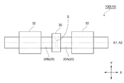
図1は、本実施形態のアンテナ装置の一例を示す模式断面図である。ここで、図1および後述する図2以降において、図中に示すX方向およびY方向は互いに直交する方向である。また、X方向は、図1中に示す2本の棒状コア20の配列方向と平行であると共に、各々の棒状コア20A(20)、20B(20)の中心軸A1、A2とも平行である。この点は、図2以降に示される棒状コアについても実質同様である。
FIG. 1 is a schematic cross-sectional view showing an example of the antenna device of this embodiment. Here, in FIG. 1 and FIG. 2 to be described later, the X direction and the Y direction shown in the drawing are directions orthogonal to each other. Further, the X direction is parallel to the arrangement direction of the two rod-shaped
図1に示す本実施形態のアンテナ装置10A(10)は、その主要部として、直列に配置された複数本(図1に示す例では2本)の棒状コア20と、導線を巻回して形成されたコイル30とを有している。また、第一の棒状コア20Aと、第一の棒状コア20Aの一方の端部側に配置された第二の棒状コア20Bとは、離間して配置されている。また、第一の棒状コア20Aと第二の棒状コア20Bとは、第一の棒状コア20Aの中心軸A1と、第二の棒状コア20Bの中心軸A2とが一致するように配置されている。
The
さらに、コイル30の内周側には、第一の棒状コア20Aの第二の棒状コア20Bが配置された側の端面22A、および、第二の棒状コア20Bの第一の棒状コア20Aが配置された側の端面22B、が位置している。
Further, on the inner peripheral side of the
また、第一の棒状コア20Aおよび第二の棒状コア20Bは、有底筒状のボビン40A(40)内に収納されている。それゆえ、コイル30は、ボビン40Aの外周面と接して設けられている。さらに、ボビン40Aの第一の棒状コア20Aが収納された側の端部近傍には、筒状のボビン本体部42の外周面よりも外側に突出する鍔部44Aが設けられており、ボビン40Aの第二の棒状コア20Bが収納された側の端部には、底蓋部44Bが設けられる。なお、底蓋部44Bは、ボビン本体部42の外周面よりも外側にも突出して設けられている。さらに、底蓋部44Bのボビン本体部42が設けられた側と反対側の面には、筒状の外部端子カバー46が設けられている。
The first rod-shaped
また、ボビン本体部42の底蓋部44B側の外周壁面の一部には開口部42Aが設けられ、この開口部42Aに露出している第二の棒状コア20Bに対向する位置には、金属端子50が配置されている。この金属端子50は、導線(不図示)によりコイル30に接続されると共に、一端が、底蓋部44Bを貫通して底蓋部44Bのボビン本体部42が設けられた側と反対側の面に露出している。そして、金属端子50の一端は、外部接続端子60に接続されている。また、金属端子50には、チップコンデンサなどのコンデンサ(不図示)が接続される。これにより、金属端子50を介してコイル30はコンデンサに電気的に接続される。さらに、金属端子50には、必要に応じてコンデンサ以外のその他の電子素子が適宜接続されていてもよい。
Further, an
さらに、ボビン40Aは、有底筒状のケース70内に、ボビン40Aの底蓋部44Bが設けられた側が、ケース70の開口部72側に位置するように収納されている。また、外部端子カバー46の外周面と、ケース70の開口部72近傍の内周面との間には、リング状のキャップ部材80が設けられている。
Further, the
なお、棒状コア20は、磁性材料から構成され、たとえば、Mn−Zn系フェライトやそれ以外のアモルファス系磁性体の微粉末を圧縮成形することにより作製された部材などを適宜用いることができる。また、コイル30等を構成する導線は、銅等の導電性材料からなる芯線と、この芯線の表面を覆う絶縁材料とを有する部材であり、金属端子50および外部接続端子60としては銅などの導電性部材からなる部材が適宜利用できる。さらに、ボビン40、ケース70およびキャップ部材80としては樹脂材料からなる部材が用いられる。たとえば、ボビン40としては、PBT(ポリブチレンテレフタレート)を用いて射出成形した部材を用いることができ、ケース70およびキャップ部材80としては、PP(ポリプロピレン)を用いて射出成形した部材を用いることができる。
The rod-shaped
本実施形態のアンテナ装置10は、図1および後述する図4、5に例示するように、第一の棒状コア20Aと第二の棒状コア20Bとが離間して配置され、かつ、コイル30の内周側に第一の棒状コア20Aの第二の棒状コア20Bが配置された側の端面22A、および、第二の棒状コア20Bの第一の棒状コア20Aが配置された側の端面22Bから選択される少なくとも一方の端面が位置する。このため、本実施形態のアンテナ装置10では、共振周波数分布の中央値と、共振周波数の設計値とのズレを抑制することが容易である。以下にこのような効果が得られる理由について説明する。
In the
図2は、直列に配置された2本の棒状コアの配列方向に沿って、配列方向の一端側から他端側へとコイルを移動させた場合について示す模式図であり、図3は、図2に示す場合において、コイルの位置に対するインダクタンス値Lを測定した結果について示すグラフである。 FIG. 2 is a schematic diagram showing a case where the coil is moved from one end side to the other end side in the arrangement direction along the arrangement direction of two rod-shaped cores arranged in series, and FIG. 6 is a graph showing the result of measuring the inductance value L with respect to the position of the coil in the case shown in FIG.
図2に示すように、2本の棒状コア100A、100Bは、各々の中心軸B1と中心軸B2とが一致するように直列に2本配置されている。そして、これら2本の棒状コア100A、100Bの配列方向(X方向)に沿って、図2(A)、図2(B)および図2(C)に示すように、棒状コア100B側から棒状コア100A側へと、コイル110を移動させた。ここで、棒状コア100A、100Bの中心軸B1、B2方向の長さは7cmとし、棒状コア100A、100Bの配列方向と平行な方向におけるコイル110の長さは4cmである。また、コイル110の位置は、棒状コア100Bの棒状コア100Aが配置された側と反対側の端面を基準位置(0cm)とした場合において、基準位置からコイル110の基準位置側の端部までの距離で示した。
As shown in FIG. 2, the two rod-shaped
ここで、図2(A)は、コイル110が基準位置から1cm離れた位置に配置された場合について示す図であり、図2(B)は、コイル110が基準位置から5cm離れた位置に配置された場合について示す図であり、図2(C)は、コイル110が基準位置から12cm離れた位置に配置された場合について示す図である。また、基準位置から7cmの位置には、第一の棒状コア100Aと第二の棒状コア100Bとの接触部X(ギャップ長さG=0mm)、あるいは、間隙部X(ギャップ長さG>0mm)が形成される。ここで、インダクタンス値Lの測定に際しては、棒状コア100Aと棒状コア100Bとのギャップ長さGを、0mm、0.2mmおよび1.0mmの3水準とし、ギャップ長さGおよび基準位置からのコイル110の位置以外のその他条件については、全て一定条件とした。
Here, FIG. 2A is a diagram showing a case where the
また、図3中、横軸はコイル110の位置(cm)であり、縦軸は、インダクタンス値L(μH)である。また、図3中に示す符号(A)、(B)および(C)で示されるインダクタンス値Lは、ぞれぞれ、図2(A)、図2(B)および図2(C)に示す位置にコイル110が配置された状態に対応している。
Further, in FIG. 3, the horizontal axis represents the position (cm) of the
図3に示す結果から明らかなように、ギャップ長さGが0mmを超える場合、インダクタンス値Lは、コイル110が第二の棒状コア100Bの中心軸B2方向の中央部に近づくに従い極大値を示した後、間隙部Xに近づくに従い低下して、さらにコイル110の長さ方向の中央部近傍に間隙部Xが位置する際に極小値となる。さらに、インダクタンス値Lは、コイル110が間隙部Xから離れて、第一の棒状コア100Aの中心軸B1方向の中央部に近づくに従い再び極大値を示し、その後、第一の棒状コア100Aの端部側(第二の棒状コア100Bが配置された側と反対側の端部)へと近づくに従い、再び低下する。すなわち、インダクタンス値Lは、コイル110の位置に対してM字状の曲線を描くように変化する。また、インダクタンス値Lの極大値と極小値との差は、ギャップ長さGが大きくなる程、顕著になる。
As is clear from the results shown in FIG. 3, when the gap length G exceeds 0 mm, the inductance value L shows a maximum value as the
すなわち、ギャップ長さGが0mmの場合、言い換えれば、2本の棒状コア100A、100Bを接続して一体化した1本の細長い棒状コアを用いているに等しい場合、コイル110の位置に関係無く、インダクタンス値Lは大きな値を取りえる。それゆえ、1Turn当りのインダクタンス値も大きくなるため、コイル110の巻回数を整数倍単位で増減させて、共振周波数を微調整することが困難である。
That is, when the gap length G is 0 mm, in other words, when it is equivalent to using one elongated rod-shaped core in which the two rod-shaped
また、2本の棒状コア100A、100B間のギャップ長さGが0mmを超える場合であっても、図2(A)および図2(C)に例示されるようにコイル110が間隙部X近傍と重複しない位置に配置されていれば、インダクタンス値Lは大きな値を取りえる。この場合も、ギャップ長さGが0mmのときと同様に、1Turn当りのインダクタンス値が大きくなるため、コイル110の巻回数を整数倍単位で増減させて、共振周波数を微調整することが困難である。
Even when the gap length G between the two rod-shaped
しかしながら、(i)ギャップ長さGが0mmを超え、かつ、(ii)図2(B)に示すようにコイル110が、間隙部X近傍と重複する位置にある場合(言い換えれば、コイル110の内周側に、第一の棒状コア100Aの第二の棒状コア100Bが配置された側の端部近傍と、第二の棒状コア100Bの第一の棒状コア100Aが配置された側の端部近傍とが位置している場合)では、インダクタンス値Lは極小値を示す。この場合、1Turn当りのインダクタンス値も小さくなるため、コイル110の巻回数を整数倍単位で増減させて、共振周波数を微調整することが容易である。
However, when (i) the gap length G exceeds 0 mm, and (ii) the
したがって、図1に示す本実施形態のアンテナ装置10Aのように、コイル30の内周側に2つの棒状コア20A、20Bの端面22A、22Bが位置するようにコイル30を配置した場合、コイル30の巻回数を整数倍単位で増減させることで、共振周波数を微調整できる。それゆえ、実際に製造された本実施形態のアンテナ装置10の共振周波数分布の中央値と、共振周波数の設計値とのズレを抑制することが容易である。
Therefore, when the
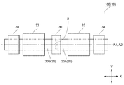
なお、図2から明らかなように、ギャップ長さGが0mmを超える場合において、インダクタンス値Lが極小値を示すのは、コイル110が、間隙部X近傍に位置するときである。また、アンテナ装置10の製造に際して、導線を巻回してコイル30を形成する際に、棒状コア20A、20Bの配列方向の一方側から他方側へと順次巻回される。これらの点を考慮すると、コイル30の形成時において、共振周波数を微調整するための調整ゾーンとなる最初の数回あるいは最後の数回の巻回位置(完成したコイル30の長さ方向のいずれか一方の端部側近傍の位置)は、第一の棒状コア20Aの第二の棒状コア20Bが配置された側の端面22Aと、第二の棒状コア20Bの第一の棒状コア20Aが配置された側の端面22Bとの間に形成される領域Sの近傍であることが最も有利であると言える。
Note that, as is clear from FIG. 2, when the gap length G exceeds 0 mm, the inductance value L exhibits a minimum value when the
それゆえ、共振周波数の微調整がより容易になるという点では、図1に例示したアンテナ装置10Aよりも、以下の図4および図5に例示するアンテナ装置10B(10)、10C(10)の方が望ましい。ここで、図4に示すアンテナ装置10Bでは、コイル30の内周側に、第二の棒状コア20Bの第一の棒状コア20Aが配置された側の端面22Bと、第二の棒状コア20Bのうち端面22B側近傍寄りの部分とが位置するようにコイル30が配置されている。そして、この点を除けば、図4に示すアンテナ装置10Bは、図1に示すアンテナ装置10Aと実質同様の構成を有している。
Therefore, in that fine adjustment of the resonance frequency becomes easier, the
また、図5に示すアンテナ装置10Cでは、コイル30の内周側に、第一の棒状コア20Aの第二の棒状コア20Bが配置された側の端面22A、および、第二の棒状コア20Bの第一の棒状コア20Aが配置された側の端面22B、が位置している。また、端面22Aと端面22Bとの間に形成される領域Sの両側近傍の第一の棒状コア20Aと第二の棒状コア20Bも、コイル30の内周側に位置しているが、コイル30は、第二の棒状コア20B側に著しく偏って配置されている。そして、これらの点を除けば、図5に示すアンテナ装置10Bは、図1に示すアンテナ装置10Aと実質同様の構成を有している。
Further, in the
図1、図4および図5に例示したように、本実施形態のアンテナ装置10では、コイル30の内周側に、第一の棒状コア20Aの第二の棒状コア20Bが配置された側の端面22A、および、第二の棒状コア20Bの第一の棒状コア20Aが配置された側の端面22B、から選択される少なくとも一方の端面が位置していればよい。しかしながら、コイル30の巻回数の調整によって共振周波数の微調整をより容易とする観点からは、棒状コア20A,20Bの配列方向において、領域Sに対して、図1に例示したようにコイル30が対称に配置されているよりも、図4および図5に例示したようにコイル30が非対称に配置されていることが望ましい。領域Sに対して、コイル30を非対称に配置することで、コイル30を形成する際に、コイル30の両端部のうち、領域Sに相対的により近い側の端部において巻回数を調整することで、共振周波数の微調整がより容易になるためである。
As illustrated in FIG. 1, FIG. 4 and FIG. 5, in the
これに加えて、コイル30のうち、領域Sに相対的により遠い側の端部近傍のコイル部分は、棒状コア20の中央部近傍に位置することになる。そして、棒状コア20の中央部近傍に位置するコイル部分は、図3に示すグラフから明らかなように、アンテナ装置10全体のインダクタンス値Lの増大にも寄与する。
In addition to this, the coil portion of the
それゆえ、領域Sに対してコイル30を非対称に配置した図4および図5に例示するアンテナ装置10B、10Cは、領域Sに対してコイル30を対称に配置した図1に例示するアンテナ装置10Aと比べて、アンテナ装置10全体としてはより大きなインダクタンス値Lを得ることが容易となる一方で、共振周波数の微調整もより容易となる。
Therefore, the
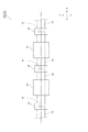
また、共振周波数の微調整が容易であることに加えて、さらに+αの機能あるいは効果を得るために、領域Sの近傍に配置されたコイル30以外のコイルをさらに用いることもできる。この場合、コイル30は、共振周波数の微調整のみを目的として、コイル30の巻回数を数Turn程度に留めるだけでもよい。このようなアンテナ装置10としては、たとえば、図6〜図8に示すアンテナ装置10D、10E、10Fが挙げられる。
Further, in addition to the fact that the fine adjustment of the resonance frequency is easy, a coil other than the
ここで、図6〜図8においては、アンテナ装置10D、10E、10Fの主要部であるコア20およびコイル30、32、34以外の部材については記載を省略してある。
Here, in FIGS. 6 to 8, members other than the core 20 and the
図6に示すアンテナ装置10Dでは、図1に示すアンテナ装置10Aに対して、第一の棒状コア20Aおよび第二の棒状コア20BのX方向中央部近傍にそれぞれコイル32がさらに配置されている。アンテナ装置10Dでは、コイル30の巻回数は数ターン程度として、共振周波数の微調整を行い、コイル30よりも巻回数のより多いコイル32によりアンテナ装置10D全体のインダクタンス値Lを大きくし、アンテナ装置10Dの出力を向上させている。
In the
図7に示すアンテナ装置10Eでは、図6に示すアンテナ装置10Dに対して、さらに2つの補助コイル34が設けられている。ここで一方の補助コイル34は、第一の棒状コア20Aのコイル30が配置された側と反対側の端部近傍に配置され、他方の補助コイル34は、第二の棒状コア20Bのコイル30が配置された側と反対側の端部近傍に配置されている。さらに2つの補助コイル34を設けることで、図7に示すアンテナ装置10Eは、図6に示すアンテナ装置10Dに対して、より大きな出力を得ることができる。
The
図8に示すアンテナ装置10Fは、図6に示すアンテナ装置10Dの変形例であり、具体的には、直列に配列された3本以上の棒状コア20を用いた場合のアンテナ装置10の一例を示したものである。ここで、図8中に示すX方向と平行を成す一点鎖線は、各々の棒状コア20の中心軸と一致する方向である。アンテナ装置10Fでは、X方向において隣り合う2本の棒状コア20の間に形成される領域S近傍にコイル30が配置されると共に、各々の棒状コア20のX方向中央部近傍にコイル32が配置される。このため、X方向に対して、コイル30とコイル32とが交互に繰り返して配置されることになる。なお、図8に示すアンテナ装置10Fでは、複数個のコイル30のうち、少なくともいずれか1つのコイル30の巻回数を調整することで共振周波数を微調整し、残りのコイル30の巻回数は全て一定とすることができる。
An
なお、図6〜図8に示すアンテナ装置10D、10E,10Fにおいて、コイル32のX方向長さは、棒状コア20のX方向長さの半分以下であることが好適である。
In the
なお、本実施形態のアンテナ装置10に用いられるコンデンサの個体間静電容量ばらつきは、特に制限されるものではないが、一般的なアンテナ装置に利用されるコンデンサの場合、±1%以上であることが実用上大きな効果を発揮できる。個体間静電容量ばらつきが±1%未満では、コンデンサの入手自体が困難になるか、あるいは、コンデンサのコストが大幅に増大するため、実用性に欠ける場合がある。また、本実施形態のアンテナ装置10では、アンテナ装置10の製造に使用するコンデンサを分類する際のランク数を削減する代わりに個体間静電容量ばらつきのより大きい安価なコンデンサを用いることも容易である。この観点では、個体間静電容量ばらつきは、±10%以上でもよい。しかしながら、個体間静電容量ばらつきが大きすぎる場合はコンデンサを多数のランクに分類した上で、各ランク毎にコイル30の巻回数を調整しなければならず、製造工程が煩雑化してしまう。このため個体間静電容量ばらつきは±5%以下が好ましい。さらに、ランク分けを単純化するためには、±3%以下であることが更に好ましい。
The capacitance variation among the capacitors used in the
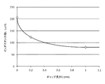
また、本実施形態のアンテナ装置10において、第一の棒状コア20Aと第二の棒状コア20Bとは離間して配置されていればよい、すなわち、ギャップ長さGは0mmを超えていればよい。しかしながら、ギャップ長さGは、0.2mm〜1.0mmが好ましく、0.3mm〜0.8mmがより好ましい。図9は、図2(B)に示すようにコイル110の位置を設定した場合における、ギャップ長さGに対するインダクタンス値の変化を示すグラフである。なお、図1、図4および図5に例示した本実施形態のアンテナ装置10でも、図2(B)に示す場合と同一または近接した位置にコイル30配置されていることから、図9に示すギャップ長さGに対するインダクタンス値の変化の傾向は、本実施形態のアンテナ装置10でも同様と言える。
Further, in the
ここで、図9に示すグラフから明らかなように、ギャップ長さGが0.2mm未満では、アンテナ装置10全体のインダクタンス値Lが大きくなり過ぎるため、コイル30の1Turn当たりのインダクタンス値も大きくなり、結果的に、共振周波数の微調整が困難となる場合がある。また、ギャップ長さGはアンテナ装置10の個体間や、同一個体であっても温度変化によりばらつくことは避け難い。それゆえ、ギャップ長さGが0.2mm未満では、ギャップ長さGに起因する1Turn当たりのインダクタンス値もばらつき易くなるため、この点でも共振周波数の微調整が困難となる場合がある。一方、ギャップ長さGが1.0mmを超えると、アンテナ装置10全体のインダクタンス値Lが小さくなり過ぎる場合がある。
Here, as is clear from the graph shown in FIG. 9, when the gap length G is less than 0.2 mm, the inductance value L of the
本実施形態のアンテナ装置10では、特許文献1に示される小型コアなどの共振周波数調整機構が不要である。このため、本実施形態のアンテナ装置10の製造方法は、特許文献1に示される小型コアなどの共振周波数調整機構を組み込む工程を省ける点を除けば特に限定されるものではないが、以下に説明する第一の製造方法または第二の製造方法が好ましい。
The
すなわち、第一の製造方法では、アンテナ装置10の製造に使用する同一品種のコンデンサを、個々のコンデンサの静電容量に応じて2ランクまたは3ランクに分類するコンデンサ分類工程と、個々のコンデンサのランクに応じて、導線の巻回数を異なる値に設定した上で、導線を巻回してコイル30を形成するコイル形成工程と、を少なくとも経ることで、本実施形態のアンテナ装置10を製造する。これにより、製造されたアンテナ装置10におけるコイル30を構成する導線の巻回数のバリエーション数は、2種類または3種類になる。たとえば、コンデンサの個体間静電容量ばらつきが±5%であるコンデンサを、静電容量が−5%以上0%未満のばらつき範囲内に属する第一クラスのコンデンサと、静電容量が0%以上5%以下のばらつき範囲内に属する第二クラスのコンデンサとの2ランクに分類した場合であれば、第一クラスのコンデンサを用いてアンテナ装置10を製造するときは、目標とする共振周波数の公差内に収まるようにコイル30の巻回数をX回に設定し、第二クラスのコンデンサを用いてアンテナ装置10を製造するときは、コイル30の巻回数をY回(但し、X≠Yであり、|X−Y|の値は1以上の整数値)に設定すればよい。この場合、第一の製造方法により製造されたアンテナ装置10では、個々のアンテナ装置のコイル30の巻回数のバリエーション数は2種類となる。
That is, in the first manufacturing method, a capacitor classification step of classifying capacitors of the same type used for manufacturing the
また、第二の製造方法では、アンテナ装置10の製造に使用する同一品種のコンデンサの個々のコンデンサの静電容量に関係無く、導線の巻回数を常に一定値に設定した状態で、導線を巻回してコイル30を形成するコイル形成工程を、を少なくとも経ることで、本実施形態のアンテナ装置10を製造する。すなわち、第二の製造方法により製造されたアンテナ装置10では、個々のアンテナ装置のコイル30の巻回数は全て同一(巻回数のバリエーション数は1種類のみ)である。
In the second manufacturing method, the conductor wire is wound in a state where the number of windings of the conductor wire is always set to a constant value, regardless of the capacitance of each capacitor of the same type of capacitor used for manufacturing the
よって、アンテナ装置10の製造に際して、第一の製造方法あるいは第二の製造方法を採用すれば、製造されたアンテナ装置10のコイル30を構成する導線の巻回数のバリエーション数が、1種類〜3種類のいずれかとなる。
Therefore, when the first manufacturing method or the second manufacturing method is adopted in manufacturing the
また、既述したように、本実施形態のアンテナ装置10では、コイル30の巻回数を整数倍単位で増減させた際の1Turn当たりのインダクタン値が小さいため、共振周波数の微調整が容易である。このため、コンデンサ分類工程においてコンデンサを静電容量に応じて分類する際のランク数を削減して2または3ランクとしたり、あるいは、コンデンサ分類工程自体を省略しても、要求される共振周波数の公差範囲内のアンテナ装置10を製造することが極めて容易である。すなわち、従来のように、コンデンサ分類工程における分類ランク数を4ランクまたは5ランクとしていた場合と比較して、アンテナ装置10の製造プロセスを簡略化できる。さらに、第二の製造方法では、コンデンサ分類工程自体が不要になるため、アンテナ装置10の製造プロセスをさらに簡略化できる。
Further, as described above, in the
以上に説明した本実施形態のアンテナ装置10では、個々のアンテナ装置10間の共振周波数のばらつきを±2%以下とすることが非常に容易であるため、共振周波数の公差が±2%以下という要求仕様にも対応することができる。但し、要求される共振周波数の公差は、アンテナ装置10の使用用途等により様々であるため、個々のアンテナ装置10間の共振周波数のばらつきは±2%を超えるものであってもよい。また、製造に使用するコンデンサの個体間静電容量ばらつきや、要求される共振周波数の公差等に応じて、アンテナ装置10の製造方法は適宜選択できるが、たとえば、(a)要求される共振周波数の公差がより狭い場合、および/または、製造に使用するコンデンサの個体間静電容量ばらつきがより大きい場合は、第一の製造方法がより好適であり、(b)要求される共振周波数の公差がより大きい場合、および/または、製造に使用するコンデンサの個体間静電容量ばらつきがより小さい場合は、第二の製造方法がより好適である。
In the
なお、図1、図4および図5には、2本の棒状コア20を用いたアンテナ装置10を例示したが、本実施形態のアンテナ装置10は、3本以上の棒状コア20を有していてもよい。この場合、複数本の棒状コア20から選択され、かつ、複数本の棒状コア20の配列方向において隣り合う位置にある少なくともいずれか2本の棒状コア20と、少なくとも1つのコイル30とが、図1、図4あるいは図5に例示したような配置関係を満たしていればよい。
Note that, although the
また、本実施形態のアンテナ装置10では、第一の棒状コア20Aと第二の棒状コア20Bとは離間して配置されていればよい、すなわち、ギャップ長さGは0mmを超えていればよい。ここで、第一の棒状コア20Aと第二の棒状コア20Bとの間には単なる隙間(すなわち、空気が占有する空間)が形成されていてもよいが、第一の棒状コア20Aと第二の棒状コア20Bとの間には、接着剤層あるいは板状の樹脂部材などから構成されるスペーサーが配置されていることが好ましい。第一の棒状コア20Aと第二の棒状コア20Bとの間に接着剤層あるいはスペーサーを設けることにより、ギャップ長さGの変動を抑制することができる。このため、特にギャップ長さGが短い領域(0mmを超え0.4mm程度、さらに好ましくは0.2mm〜0.4mm程度)において、インダクタンス値L、さらには共振周波数のばらつきを抑制することが極めて容易になる。
Further, in the
なお、ボビン40内に仕切り板を設けることで、この仕切り板をスペーサーとして利用することもできる。図10は、本実施形態のアンテナ装置10に用いられるボビンの他の例を示す外観斜視図である。ここで、図10中、X方向、Y方向およびZ方向は互いに直交する方向である。図10に示すボビン40B(40)は、ボビン本体部42内を、その長手方向に等間隔で分割するようにボビン本体部42内に配置される4枚の仕切り板48を備えている。また、ボビン本体部42の開口部42A(図10中、不図示)が設けられた側と反対側の面の全面は、開口部42Bが設けられている。そして、これらの点を除けば、ボビン40Bは、実質的に図1、図4および図5に示すボビン40Aと同様の構造を有する。
By providing a partition plate inside the
図10に示すボビン40Bを用いる場合、底蓋部44Bと仕切り板48Aとの間、仕切り板48Aと仕切り板48Bとの間、仕切り板48Bと仕切り板48Cとの間、および、仕切り板48Cと仕切り板48Dとの間に棒状コア20を配置することで、ボビン40B内に合計4本の棒状コア20を直列に配置することができる。また、コイル30は、コイル30の内周側に、4つの仕切り板48から選択される少なくともいずれかの仕切り板48と、この仕切り板48の両側に配置された棒状コア20の仕切り板48側の端部近傍とが位置するように配置される。
When using the
図10に例示したような仕切り板48を備えたボビン40Bでは、ボビン40B内に、複数本の棒状コア20を容易、かつ、安定して保持することができる。また、ボビン本体部42の一方の面の全面が、ボビン本体部42を構成する外周壁面を取り除いて形成された開口部42Bとなっている。このため、ボビン本体部42をより薄型化することができると共に、同一方向から、複数本の棒状コア20を同時にボビン40B内に挿入して配置することができる。これに加えて、樹脂材料と金型とを用いてボビン40Bを成形する際に用いる金型も簡易かつ安価に作製できる。なお、ボビン40Bに巻線する際の遠心力を考慮すると、その開口部42Bを塞ぐ蓋部材や、適切な噛合部材を用いるなど、この分野における常用技術をさらに用いてもよい。
In the
10、10A、10B、10C、10D、10E、10F :アンテナ装置
20 :棒状コア
20A :(第一の)棒状コア
20B :(第二の)棒状コア
30 :コイル
32 :コイル
34 :(補助)コイル
40、40A,40B :ボビン
42 :ボビン本体部
42A、42B :開口部
44A :鍔部
44B :底蓋部
46 :外部端子カバー
48、48A、48B、48C、48D :仕切り板
50 :金属端子
60 :外部接続端子
70 :ケース
72 :開口部
80 :キャップ部材
100A :(第一の)棒状コア
100B :(第二の)棒状コア
110 :コイル
200 :棒状コア
202A :(第一の)棒状コア
202B :(第二の)棒状コア
210 :コイル
10, 10A, 10B, 10C, 10D, 10E, 10F: Antenna device 20:
Claims (9)
導線を巻回して形成されたコイルと、
前記コイルに電気的に接続されたコンデンサと、を少なくとも備え、
前記複数本の棒状コアから選択された第一の棒状コアと、前記複数本の棒状コアから選択され、かつ、前記第一の棒状コアのいずれか一方の端部側に配置された第二の棒状コアとが、離間して配置され、
前記コイルの内周側に、前記第一の棒状コアの前記第二の棒状コアが配置された側の端面、および、前記第二の棒状コアの前記第一の棒状コアが配置された側の端面、から選択される少なくとも一方の端面が位置し、かつ、
前記コイルの軸方向長さが、前記第一の棒状コアの軸方向長さおよび前記第二の棒状コアの軸方向長さよりも短いことを特徴とするアンテナ装置。 A plurality of rod-shaped cores arranged in series,
A coil formed by winding a conducting wire,
At least a capacitor electrically connected to the coil,
A first rod-shaped core selected from the plurality of rod-shaped cores and a second rod-shaped core selected from the plurality of rod-shaped cores, and a second one disposed on one end side of one of the first rod-shaped cores The rod-shaped core and the separated ,
On the inner peripheral side of the coil, an end face of the first rod-shaped core on which the second rod-shaped core is arranged, and a side of the second rod-shaped core on which the first rod-shaped core is arranged. At least one end face selected from the end faces is located , and
An antenna device , wherein an axial length of the coil is shorter than an axial length of the first rod-shaped core and an axial length of the second rod-shaped core .
前記個々のコンデンサのランクに応じて、導線の巻回数を異なる値に設定した上で、前記導線を巻回してコイルを形成するコイル形成工程と、を少なくとも経て、
請求項1〜7のいずれか1つに記載のアンテナ装置を製造することを特徴とするアンテナ装置の製造方法。 A capacitor classification process for classifying capacitors of the same type used for manufacturing antenna devices into two ranks or three ranks according to the capacitance of each capacitor;
Depending on the rank of the individual capacitors, after setting the number of turns of the conductive wire to different values, at least through a coil forming step of winding the conductive wire to form a coil,
A method for manufacturing an antenna device, comprising manufacturing the antenna device according to claim 1 .
請求項1〜7のいずれか1つに記載のアンテナ装置を製造することを特徴とするアンテナ装置の製造方法。 A coil forming step of forming a coil by winding the conducting wire in a state where the number of windings of the conducting wire is always set to a constant value irrespective of the capacitance of each capacitor of the same type of capacitor used for manufacturing the antenna device. At least,
A method for manufacturing an antenna device, comprising manufacturing the antenna device according to claim 1 .
Priority Applications (4)
| Application Number | Priority Date | Filing Date | Title |
|---|---|---|---|
| JP2016235337A JP6750488B2 (en) | 2016-12-02 | 2016-12-02 | Antenna device and manufacturing method thereof |
| EP17184517.5A EP3331098B1 (en) | 2016-12-02 | 2017-08-02 | Antenna device and manufacturing method for the same |
| US15/672,740 US10305188B2 (en) | 2016-12-02 | 2017-08-09 | Antenna device and manufacturing method for the same |
| CN201710682940.7A CN108155481B (en) | 2016-12-02 | 2017-08-10 | Antenna device and method of manufacturing the same |
Applications Claiming Priority (1)
| Application Number | Priority Date | Filing Date | Title |
|---|---|---|---|
| JP2016235337A JP6750488B2 (en) | 2016-12-02 | 2016-12-02 | Antenna device and manufacturing method thereof |
Publications (2)
| Publication Number | Publication Date |
|---|---|
| JP2018093371A JP2018093371A (en) | 2018-06-14 |
| JP6750488B2 true JP6750488B2 (en) | 2020-09-02 |
Family
ID=59520815
Family Applications (1)
| Application Number | Title | Priority Date | Filing Date |
|---|---|---|---|
| JP2016235337A Active JP6750488B2 (en) | 2016-12-02 | 2016-12-02 | Antenna device and manufacturing method thereof |
Country Status (4)
| Country | Link |
|---|---|
| US (1) | US10305188B2 (en) |
| EP (1) | EP3331098B1 (en) |
| JP (1) | JP6750488B2 (en) |
| CN (1) | CN108155481B (en) |
Families Citing this family (6)
| Publication number | Priority date | Publication date | Assignee | Title |
|---|---|---|---|---|
| JP6645622B2 (en) * | 2017-05-25 | 2020-02-14 | 株式会社村田製作所 | Antenna device |
| EP3723196B1 (en) | 2019-04-12 | 2023-07-12 | Schaffner EMV AG | Antenna |
| EP3726651B1 (en) | 2019-04-15 | 2026-04-22 | TE Connectivity Solutions GmbH | Antenna |
| EP3731343A1 (en) | 2019-04-25 | 2020-10-28 | Schaffner EMV AG | Antenna |
| CN114239764B (en) * | 2021-10-26 | 2024-07-12 | 北京瑞芯谷科技有限公司 | Radio frequency tag identifier, manufacturing method, application and RFID management system |
| EP4447222A1 (en) | 2023-04-13 | 2024-10-16 | Schaffner EMV AG | An antenna and method for manufacturing an antenna |
Family Cites Families (10)
| Publication number | Priority date | Publication date | Assignee | Title |
|---|---|---|---|---|
| JPH0927708A (en) * | 1995-07-13 | 1997-01-28 | Tokai Rika Co Ltd | Coil |
| JP2002261536A (en) * | 2001-03-02 | 2002-09-13 | Alps Electric Co Ltd | Small-sized antenna and its manufacturing method |
| US7135978B2 (en) * | 2001-09-14 | 2006-11-14 | Calypso Medical Technologies, Inc. | Miniature resonating marker assembly |
| JP4523437B2 (en) * | 2005-02-01 | 2010-08-11 | セイコーインスツル株式会社 | Method for manufacturing antenna structure |
| JP2007043588A (en) | 2005-08-05 | 2007-02-15 | Murata Mfg Co Ltd | Coil antenna |
| JP5527218B2 (en) * | 2008-12-19 | 2014-06-18 | 日立金属株式会社 | Resonant receiving antenna and receiving apparatus |
| JP5275959B2 (en) * | 2009-11-17 | 2013-08-28 | 株式会社ワコム | Coil, position indicator, position detection device, and coil winding method |
| JP5738744B2 (en) * | 2011-11-15 | 2015-06-24 | 株式会社東芝 | Resonator and wireless power transmission device |
| CN104303364B (en) * | 2012-06-21 | 2016-08-24 | 东光株式会社 | rod antenna |
| DE102013222435B4 (en) * | 2013-11-05 | 2019-06-06 | SUMIDA Components & Modules GmbH | Magnetic core element, magnetic core module and an inductive component using the magnetic core module |
-
2016
- 2016-12-02 JP JP2016235337A patent/JP6750488B2/en active Active
-
2017
- 2017-08-02 EP EP17184517.5A patent/EP3331098B1/en active Active
- 2017-08-09 US US15/672,740 patent/US10305188B2/en active Active
- 2017-08-10 CN CN201710682940.7A patent/CN108155481B/en active Active
Also Published As
| Publication number | Publication date |
|---|---|
| CN108155481A (en) | 2018-06-12 |
| CN108155481B (en) | 2020-09-22 |
| EP3331098A1 (en) | 2018-06-06 |
| US20180159224A1 (en) | 2018-06-07 |
| EP3331098B1 (en) | 2020-07-15 |
| US10305188B2 (en) | 2019-05-28 |
| JP2018093371A (en) | 2018-06-14 |
Similar Documents
| Publication | Publication Date | Title |
|---|---|---|
| JP6750488B2 (en) | Antenna device and manufacturing method thereof | |
| CN111933388B (en) | Coil component | |
| JP5913268B2 (en) | 3-axis antenna | |
| JP2023134676A (en) | stylus pen | |
| JP2000036414A (en) | Inductor and manufacture thereof | |
| JP6547373B2 (en) | Coil device and method of manufacturing coil device | |
| JP6453787B2 (en) | Winding unit | |
| CN107293859A (en) | A kind of manufacture method of antenna assembly and the antenna assembly | |
| JP6520187B2 (en) | Coil parts | |
| CN107077953B (en) | Coil arragement construction and transformer with low interwinding capacity | |
| US12567532B2 (en) | Inductor | |
| JP6379468B2 (en) | Wire wound electronic components | |
| CN103823579A (en) | Coil arrangement for electronic pen | |
| CN108369854B (en) | winding device | |
| JP6794760B2 (en) | Antenna device | |
| KR101995216B1 (en) | Bobbin and Toroidal Inductor Comprising the Same | |
| JP2014220292A (en) | Inductor and method of manufacturing the same | |
| JP2016106436A (en) | Dust inductor | |
| JP7645199B2 (en) | Inductive components and methods for adjusting inductance - Patents.com | |
| KR102816635B1 (en) | Ultra-Slim inductor | |
| CN114072886A (en) | Inductor | |
| WO2021010071A1 (en) | Inductor | |
| JP6736890B2 (en) | Inductor | |
| JP6332160B2 (en) | Surface mount inductor and manufacturing method thereof | |
| US10262780B2 (en) | Analytical instrument inductors and methods for manufacturing same |
Legal Events
| Date | Code | Title | Description |
|---|---|---|---|
| A621 | Written request for application examination |
Free format text: JAPANESE INTERMEDIATE CODE: A621 Effective date: 20190329 |
|
| A977 | Report on retrieval |
Free format text: JAPANESE INTERMEDIATE CODE: A971007 Effective date: 20200123 |
|
| A131 | Notification of reasons for refusal |
Free format text: JAPANESE INTERMEDIATE CODE: A131 Effective date: 20200128 |
|
| A521 | Request for written amendment filed |
Free format text: JAPANESE INTERMEDIATE CODE: A523 Effective date: 20200226 |
|
| TRDD | Decision of grant or rejection written | ||
| A01 | Written decision to grant a patent or to grant a registration (utility model) |
Free format text: JAPANESE INTERMEDIATE CODE: A01 Effective date: 20200714 |
|
| A61 | First payment of annual fees (during grant procedure) |
Free format text: JAPANESE INTERMEDIATE CODE: A61 Effective date: 20200727 |
|
| R150 | Certificate of patent or registration of utility model |
Ref document number: 6750488 Country of ref document: JP Free format text: JAPANESE INTERMEDIATE CODE: R150 |
|
| S531 | Written request for registration of change of domicile |
Free format text: JAPANESE INTERMEDIATE CODE: R313531 |
|
| R350 | Written notification of registration of transfer |
Free format text: JAPANESE INTERMEDIATE CODE: R350 |
|
| R250 | Receipt of annual fees |
Free format text: JAPANESE INTERMEDIATE CODE: R250 |
|
| R250 | Receipt of annual fees |
Free format text: JAPANESE INTERMEDIATE CODE: R250 |
|
| R250 | Receipt of annual fees |
Free format text: JAPANESE INTERMEDIATE CODE: R250 |