JP6749849B2 - Additive deposition system and method - Google Patents
Additive deposition system and method Download PDFInfo
- Publication number
- JP6749849B2 JP6749849B2 JP2017003656A JP2017003656A JP6749849B2 JP 6749849 B2 JP6749849 B2 JP 6749849B2 JP 2017003656 A JP2017003656 A JP 2017003656A JP 2017003656 A JP2017003656 A JP 2017003656A JP 6749849 B2 JP6749849 B2 JP 6749849B2
- Authority
- JP
- Japan
- Prior art keywords
- substrate
- aerosol
- charged
- polarity
- charge
- Prior art date
- Legal status (The legal status is an assumption and is not a legal conclusion. Google has not performed a legal analysis and makes no representation as to the accuracy of the status listed.)
- Active
Links
Images


Classifications
-
- B—PERFORMING OPERATIONS; TRANSPORTING
- B33—ADDITIVE MANUFACTURING TECHNOLOGY
- B33Y—ADDITIVE MANUFACTURING, i.e. MANUFACTURING OF THREE-DIMENSIONAL [3-D] OBJECTS BY ADDITIVE DEPOSITION, ADDITIVE AGGLOMERATION OR ADDITIVE LAYERING, e.g. BY 3-D PRINTING, STEREOLITHOGRAPHY OR SELECTIVE LASER SINTERING
- B33Y10/00—Processes of additive manufacturing
-
- B—PERFORMING OPERATIONS; TRANSPORTING
- B29—WORKING OF PLASTICS; WORKING OF SUBSTANCES IN A PLASTIC STATE IN GENERAL
- B29C—SHAPING OR JOINING OF PLASTICS; SHAPING OF MATERIAL IN A PLASTIC STATE, NOT OTHERWISE PROVIDED FOR; AFTER-TREATMENT OF THE SHAPED PRODUCTS, e.g. REPAIRING
- B29C64/00—Additive manufacturing, i.e. manufacturing of three-dimensional [3D] objects by additive deposition, additive agglomeration or additive layering, e.g. by 3D printing, stereolithography or selective laser sintering
- B29C64/10—Processes of additive manufacturing
- B29C64/106—Processes of additive manufacturing using only liquids or viscous materials, e.g. depositing a continuous bead of viscous material
- B29C64/112—Processes of additive manufacturing using only liquids or viscous materials, e.g. depositing a continuous bead of viscous material using individual droplets, e.g. from jetting heads
-
- B—PERFORMING OPERATIONS; TRANSPORTING
- B29—WORKING OF PLASTICS; WORKING OF SUBSTANCES IN A PLASTIC STATE IN GENERAL
- B29C—SHAPING OR JOINING OF PLASTICS; SHAPING OF MATERIAL IN A PLASTIC STATE, NOT OTHERWISE PROVIDED FOR; AFTER-TREATMENT OF THE SHAPED PRODUCTS, e.g. REPAIRING
- B29C64/00—Additive manufacturing, i.e. manufacturing of three-dimensional [3D] objects by additive deposition, additive agglomeration or additive layering, e.g. by 3D printing, stereolithography or selective laser sintering
- B29C64/10—Processes of additive manufacturing
- B29C64/106—Processes of additive manufacturing using only liquids or viscous materials, e.g. depositing a continuous bead of viscous material
- B29C64/118—Processes of additive manufacturing using only liquids or viscous materials, e.g. depositing a continuous bead of viscous material using filamentary material being melted, e.g. fused deposition modelling [FDM]
-
- B—PERFORMING OPERATIONS; TRANSPORTING
- B29—WORKING OF PLASTICS; WORKING OF SUBSTANCES IN A PLASTIC STATE IN GENERAL
- B29C—SHAPING OR JOINING OF PLASTICS; SHAPING OF MATERIAL IN A PLASTIC STATE, NOT OTHERWISE PROVIDED FOR; AFTER-TREATMENT OF THE SHAPED PRODUCTS, e.g. REPAIRING
- B29C64/00—Additive manufacturing, i.e. manufacturing of three-dimensional [3D] objects by additive deposition, additive agglomeration or additive layering, e.g. by 3D printing, stereolithography or selective laser sintering
- B29C64/20—Apparatus for additive manufacturing; Details thereof or accessories therefor
- B29C64/205—Means for applying layers
- B29C64/209—Heads; Nozzles
-
- B—PERFORMING OPERATIONS; TRANSPORTING
- B29—WORKING OF PLASTICS; WORKING OF SUBSTANCES IN A PLASTIC STATE IN GENERAL
- B29C—SHAPING OR JOINING OF PLASTICS; SHAPING OF MATERIAL IN A PLASTIC STATE, NOT OTHERWISE PROVIDED FOR; AFTER-TREATMENT OF THE SHAPED PRODUCTS, e.g. REPAIRING
- B29C64/00—Additive manufacturing, i.e. manufacturing of three-dimensional [3D] objects by additive deposition, additive agglomeration or additive layering, e.g. by 3D printing, stereolithography or selective laser sintering
- B29C64/20—Apparatus for additive manufacturing; Details thereof or accessories therefor
- B29C64/245—Platforms or substrates
-
- B—PERFORMING OPERATIONS; TRANSPORTING
- B29—WORKING OF PLASTICS; WORKING OF SUBSTANCES IN A PLASTIC STATE IN GENERAL
- B29C—SHAPING OR JOINING OF PLASTICS; SHAPING OF MATERIAL IN A PLASTIC STATE, NOT OTHERWISE PROVIDED FOR; AFTER-TREATMENT OF THE SHAPED PRODUCTS, e.g. REPAIRING
- B29C64/00—Additive manufacturing, i.e. manufacturing of three-dimensional [3D] objects by additive deposition, additive agglomeration or additive layering, e.g. by 3D printing, stereolithography or selective laser sintering
- B29C64/30—Auxiliary operations or equipment
-
- B—PERFORMING OPERATIONS; TRANSPORTING
- B29—WORKING OF PLASTICS; WORKING OF SUBSTANCES IN A PLASTIC STATE IN GENERAL
- B29K—INDEXING SCHEME ASSOCIATED WITH SUBCLASSES B29B, B29C OR B29D, RELATING TO MOULDING MATERIALS OR TO MATERIALS FOR MOULDS, REINFORCEMENTS, FILLERS OR PREFORMED PARTS, e.g. INSERTS
- B29K2995/00—Properties of moulding materials, reinforcements, fillers, preformed parts or moulds
- B29K2995/0003—Properties of moulding materials, reinforcements, fillers, preformed parts or moulds having particular electrical or magnetic properties, e.g. piezoelectric
-
- B—PERFORMING OPERATIONS; TRANSPORTING
- B33—ADDITIVE MANUFACTURING TECHNOLOGY
- B33Y—ADDITIVE MANUFACTURING, i.e. MANUFACTURING OF THREE-DIMENSIONAL [3-D] OBJECTS BY ADDITIVE DEPOSITION, ADDITIVE AGGLOMERATION OR ADDITIVE LAYERING, e.g. BY 3-D PRINTING, STEREOLITHOGRAPHY OR SELECTIVE LASER SINTERING
- B33Y30/00—Apparatus for additive manufacturing; Details thereof or accessories therefor
Description
部品の特別注文による製造は、成長産業であり、広い範囲の応用を有している。伝統的に、射出成形機および他の機械加工技術が、物体のモデルを生成し、あるいは物体そのものを生成するために使用された。より具体的には、ガラス、金属、熱可塑性物質、および他のポリマーなどの加熱された材料が、所望の物体の形状に特定的に形成された射出成形金型へと注入される。材料は、金型内で冷え、金型の形状を獲得し、物体を形成することができる。射出成形金型は、高価かつ生成に時間がかかり、物体の形状の変更に、物体の生成の時間および費用をさらに増すことなく対応することが、困難である。 Custom manufacturing of parts is a growing industry and has a wide range of applications. Traditionally, injection molding machines and other machining techniques have been used to generate models of objects or the objects themselves. More specifically, heated materials such as glass, metals, thermoplastics, and other polymers are injected into an injection mold that is specifically shaped to the desired object shape. The material can cool in the mold, acquire the shape of the mold and form an object. Injection molds are expensive and time consuming to produce, and it is difficult to accommodate changes in the shape of the object without further increasing the time and expense of creating the object.
付加製造産業が、モデルまたは物体そのものを生成するための射出成形金型の変更における費用、時間、および困難に応答して生まれた。公知の付加製造技術として、とりわけ、融合堆積モデリング(FDM)、ステレオリソグラフィ(SLA)、選択的レーザ焼結(SLS)、および噴き付けシステムが挙げられる。公知の付加製造技術の各々は、熱可塑性材料一式を用いた小規模の生産、特別注文による製造、および試作を妨げる材料、費用、および/または許容量における制限を有している。さらに、公知の付加製造技術は、射出成形などの伝統的な技術によって生み出される良質な物体の機械的特性、表面仕上げ、および造作の複製を有する部品を、正確に生成することが不可能である。 The additive manufacturing industry has spawned in response to the cost, time, and difficulty in changing injection molds to produce models or objects themselves. Known additive manufacturing techniques include fusion deposition modeling (FDM), stereolithography (SLA), selective laser sintering (SLS), and spray systems, among others. Each of the known additive manufacturing techniques has limitations in materials, cost, and/or capacity that impede small-scale production, customized manufacturing, and prototyping with a set of thermoplastic materials. Moreover, known additive manufacturing techniques are incapable of accurately producing parts with good quality mechanical properties, surface finishes, and replicas of features produced by traditional techniques such as injection molding. ..
付加製造では用途に見合った充分な性能の部品が生み出されない状況において、低コストな工具類を使用する高速コンピュータ数値制御(CNC)機械加工および高速射出成形の全産業が生まれている。しかしながら、これらの技術は、付加製造技術と比べて著しく高価であり、固有のプロセス制約を有している。 In a situation where additive manufacturing does not produce sufficient performance parts to suit the application, the entire industry of high speed computer numerical control (CNC) machining and high speed injection molding using low cost tools has sprung up. However, these techniques are significantly more expensive than the additive manufacturing techniques and have inherent process constraints.
業界は、射出成形などの伝統的であるが高価であり、柔軟性に欠け、時間のかかる技術によって生み出される高品質かつ大量に生産できる物体と、生み出される物体の品質が高くなく、おそらくは所望の構造的な完全性を備えておらず、場合によっては所望の材料によることができないが、より高い速度および柔軟性を有する付加製造技術との間で、決定を強いられている。例えば、FDMおよびSLSは、使用できる材料の種類に制限があり、100%の密度の物体を生み出さない。高速CNCモデリングは、優秀な細部の造作および仕上げを有するより良好な品質の物体を有するが、依然として高価である。公知の付加製造技術によって生成される試作品は、多くの場合、最終的な設計が選択されるまで改良され、最終的な設計が選択された時点で、射出成形金型が、大規模の高品質な射出成形による製造のために生成される。そのような多段階の製造プロセスも、やはり時間がかかり、高価である。 The industry has found that the traditional but expensive, inflexible, inflexible, time-consuming techniques such as injection molding produce high-quality, high-volume objects, and the quality of the produced objects is not high enough to be It lacks structural integrity and, in some cases, cannot depend on the desired material, but is forced to make decisions with additive manufacturing techniques that have higher speed and flexibility. For example, FDM and SLS are limited in the types of materials that can be used and do not produce 100% density objects. Fast CNC modeling has better quality objects with excellent detailing and finishing, but is still expensive. Prototypes produced by known additive manufacturing techniques are often refined until a final design is selected, at which point the injection mold can be scaled to a large scale. Produced for quality injection molding manufacturing. Such multi-step manufacturing processes are also time consuming and expensive.
製造産業は、広範な熱可塑性材料一式によるデジタル的な付加製造の利点ならびにより伝統的な製造技術を使用して得られる複雑さおよび構造的な完全性を有する物体を製造することができる造作の分解能を実現する製造プロセスから、恩恵を得ると考えられる。 The manufacturing industry is capable of producing objects with the advantages of digital additive manufacturing with a wide range of thermoplastic materials, as well as the complexity and structural integrity obtained using more traditional manufacturing techniques. It is believed to benefit from manufacturing processes that achieve resolution.
本明細書に示される態様によれば、さまざまな付加材料を使用し、それらを高分解能なやり方で基板の全体に堆積させることができる付加堆積のシステムおよび方法が提供される。さらに、本システムは、付加材料のプロセスを繰り返すことによって付加材料のマトリクスを生成することができる。 Aspects provided herein provide systems and methods of additive deposition that can use a variety of additive materials and deposit them over a substrate in a high resolution manner. Further, the system can generate a matrix of add-on material by repeating the process of add-on material.
図1が、本発明の実施形態による典型的な付加堆積プロセス100である。本プロセスは、エアロゾル化させた液体の付加材料の基板への選択的な堆積を、エアロゾルの液滴と基板層表面の選択された部分との間の帯電電位の差を使用して行う。付加材料は、液体であってよく、あるいは液体の状態へと融解した固体材料など、材料の液体形態であってよい。付加材料は、熱可塑性物質などのポリマーを含む任意のいくつかの材料であってよい。材料は、最初にエアロゾルとされ、エアロゾルを、選択的な堆積プロセスにおいて形成することができる。基板層表面への付加材料の選択的な堆積は、未堆積の付加材料を再びプロセス100へと再循環させて再利用することができるがゆえに付加材料の余分な堆積が実質的に抑えられるため、きわめて効率的なプロセスをもたらす。さらに、表面の電荷密度を選択し、液滴の電荷を制御することによって、各々の反復において堆積させられる材料の量を制御することができる。加えて、プロセス100は、選択的に除去される電荷の分解能にもとづく堆積に関する分解能または細かさを有する。これは、付加プロセス100が電荷密度およびプロセスの帯電変更部分の分解能にもとづいて高い分解能の水準を達成することを可能にする。付加材料の繰り返しの堆積を、付加材料で作られる三次元のマトリクスまたは物体の生成に使用することができる。
FIG. 1 is a typical
付加材料の液体エアロゾルを、さまざまなやり方で生み出すことができる。例として、図1において、エアロゾルは、フィラメント伸長式霧化器を使用して生成102される。フィラメント伸長式霧化器は、反対向きに回転する1対のローラを使用し、液状の流動化させた付加材料のフィラメントをローラの下流側の離れていく表面の間で引き延ばすことによって、エアロゾルを生成する。典型的な実施形態において、付加材料は、加熱および溶融によって液状とされる熱可塑性ポリマーであってよい。液状の付加材料は、ニップ、すなわち1対のローラの間の空間の上流側にたまり、ローラが互いに反対向きに回転するにつれてニップへと引き込まれる。下流側において、流体は、流体の一部をローラの互いに遠ざかる表面に依然として付着させたまま、ローラの互いに遠ざかる表面の間でフィラメントへと引き伸ばされる。流体フィラメントが引き伸ばされるにつれて、フィラメントは、より長く、かつより細くなる。流体フィラメントが不安定の点、すなわち流体フィラメントの毛管破壊点に達すると、フィラメントが複数の液滴へと分解する。ローラが互いに反対方向に回転するとき、ローラの表面における流体フィラメントの連続的な形成および分解が、付加材料の液滴のエアロゾルを生み出す。次いで、付加材料のエアロゾルは、基板への堆積のためにプロセスのさらなる部分へと向けられる。離れるピストン、共回転ローラ、およびローラとベルトとからなる構成など、他のフィラメント伸長式霧化器も、使用可能である。 The liquid aerosol of additive material can be produced in various ways. By way of example, in FIG. 1, the aerosol is produced 102 using a filament-expanding atomizer. Filament extension atomizers use a pair of counter-rotating rollers to draw an aerosol by stretching a filament of liquid, fluidized, additive material between the separating surfaces downstream of the rollers. To generate. In an exemplary embodiment, the add-on material may be a thermoplastic polymer that is liquefied by heating and melting. Liquid add-on material accumulates upstream of the nip, the space between the pair of rollers, and is drawn into the nip as the rollers rotate in opposite directions. Downstream, the fluid is drawn into filaments between the distanced surfaces of the rollers, while still leaving some of the fluid attached to the distanced surfaces of the rollers. As the fluid filament is stretched, it becomes longer and thinner. When the fluid filament reaches the point of instability, ie, the capillary break point of the fluid filament, the filament breaks up into droplets. As the rollers rotate in opposite directions, the continuous formation and decomposition of fluid filaments on the surface of the rollers produces an aerosol of droplets of additional material. The additive material aerosol is then directed to further portions of the process for deposition on the substrate. Other filament elongating atomizers, such as separate pistons, co-rotating rollers, and roller and belt configurations, can also be used.
随意により、形成された複数の液滴を、液滴のサイズまたは他の物理的パラメータにもとづいて選択的にフィルタ処理104することができる。複数の液滴の選択可能な物理的パラメータとして、液滴のサイズおよび/または重量を挙げることができる。スクリーンフィルタを、所望の物理的パラメータに合致する液滴を選択するために使用することができる。あるいは、慣性衝突装置あるいは他の装置または方法を、所望の物理的パラメータに合致する液滴を選択するために使用することができる。 Optionally, the formed plurality of droplets can be selectively filtered 104 based on droplet size or other physical parameters. The selectable physical parameters of the plurality of droplets can include droplet size and/or weight. Screen filters can be used to select droplets that match the desired physical parameters. Alternatively, an inertial impingement device or other device or method can be used to select droplets that meet the desired physical parameters.
付加材料の液滴のエアロゾルは、基板層表面への堆積の準備において、第1の極性へと静電的に帯電106させられる。エアロゾル帯電装置を使用することで、エアロゾルの液滴を、帯電装置を通って運ばれ、あるいは帯電装置によって運ばれるときに、帯電させることができる。例えば、エアロゾルを、コロナが封じ込まれている領域またはイオン電流が流れている領域を通過させること、液滴からの電子の放出を喚起する電離放射線を使用すること、あるいは他の手段によって、静電的に帯電させることができる。 The aerosol of droplets of the additive material is electrostatically charged 106 to the first polarity in preparation for deposition on the substrate layer surface. By using an aerosol charging device, aerosol droplets can be charged as they are carried through or by the charging device. For example, aerosols may be struck by passing through areas where coronas are contained or areas where ionic currents are flowing, using ionizing radiation to stimulate the emission of electrons from droplets, or by other means. It can be electrically charged.
基板層表面を、基板層表面の電荷の選択的な変更112に先立って、一様な帯電プロセス110に曝すことができる。基板帯電プロセス110は、基板層の表面を一様に静電的に帯電させる。すなわち、基板層の表面が、帯電したエアロゾルと反対または同じであってよい極性で、所望の電荷密度へと一様に帯電させられる。基板帯電装置を、基板層表面を静電的に帯電させるために使用することができる。そのような装置は、コロトロン、スコロトロン、または他のコロナ放電装置を備えることができる。コロナ放電装置は、基板層表面を一様に静電的に帯電させるイオンの放出を生じさせる。
The substrate layer surface can be exposed to a
基板が付加材料のエアロゾルの極性とは反対の極性へと静電的に帯電させられる例では、基板の表面の帯電の一部を、実質的に中性な状態へと選択的に変化させることができる。基板層表面の電荷を選択的に変化させることで、帯電したエアロゾルが引き付けられることがなく、あるいは静電力によって堆積させられることがない基板層表面の実質的に中性な部分が生み出される。すなわち、帯電したエアロゾルは、基板のうちの帯電したままの部分にのみ、静電力によって選択的に堆積させられる。付加材料のエアロゾルと基板とが反対の極性を有しているため、両者の間に電位が存在する。静電位が、帯電したエアロゾルを基板層表面の反対に帯電した部分へと引き付け、あるいは堆積させる静電力を生じさせる。帯電したエアロゾルは、帯電したエアロゾルと帯電した基板層表面との間の静電位が臨界点まで減少するまで、継続的に基板層表面へと引き付けられ、あるいは堆積させられる。ひとたび帯電したエアロゾルと基板表面層との間の静電位が臨界点まで弱まると、静電力も弱くなり、したがってさらなる帯電したエアロゾルが帯電した基板表面層へと引き付けられることが、実質的になくなる。 In the example where the substrate is electrostatically charged to a polarity opposite to that of the additive aerosol, selectively changing some of the charge on the surface of the substrate to a substantially neutral state. You can The selective alteration of the charge on the surface of the substrate layer creates a substantially neutral portion of the surface of the substrate layer that is not attracted by charged aerosols or deposited by electrostatic forces. That is, the charged aerosol is selectively deposited by electrostatic forces only on the portion of the substrate that remains charged. Since the aerosol of the additional material and the substrate have opposite polarities, an electric potential exists between them. The electrostatic potential creates an electrostatic force that attracts or deposits the charged aerosol to the oppositely charged portion of the substrate layer surface. The charged aerosol is continuously attracted to or deposited on the substrate layer surface until the electrostatic potential between the charged aerosol and the charged substrate layer surface decreases to a critical point. Once the electrostatic potential between the charged aerosol and the substrate surface layer weakens to a critical point, the electrostatic forces also weaken, thus substantially eliminating the further charged aerosol from being attracted to the charged substrate surface layer.
帯電したエアロゾルと帯電した基板表面層との間の静電位の大きさおよび静電力の強さは、電荷密度および帯電したエアロゾルを帯電した基板表面層から隔てている距離にもとづく。基板表面層の電荷密度を変えることで、基板層表面へと堆積させられる付加材料の量が変化する。帯電した材料が堆積させられ、あるいは引き付けられるにつれて、帯電したエアロゾルと基板層表面との間の静電位は、基板層表面の帯電が堆積させられた帯電した付加材料によって中和されるため、減少する。基板層表面の帯電を選択的に変更することによって、付加材料の選択的な堆積の領域を限定できるだけでなく、堆積させられる付加材料の量も、同様に限定することができる。基板表面層のうちの同様に帯電した部分または領域の帯電を選択的に減らすことで、それらの領域への同様に帯電した付加材料の堆積が少なくなる。 The magnitude of the electrostatic potential and the strength of the electrostatic force between the charged aerosol and the charged substrate surface layer are based on the charge density and the distance separating the charged aerosol from the charged substrate surface layer. Changing the charge density of the substrate surface layer changes the amount of additional material deposited on the substrate surface. As the charged material is deposited or attracted, the electrostatic potential between the charged aerosol and the substrate layer surface is reduced because the charge on the substrate layer surface is neutralized by the deposited charged additive material. To do. By selectively altering the charging of the substrate layer surface, not only can the area of selective deposition of additional material be limited, but the amount of additional material deposited can be limited as well. Selectively reducing the charging of similarly charged portions or regions of the substrate surface layer reduces the deposition of similarly charged additional material on those regions.
イオノグラフィック印刷ヘッドまたは他のイオン堆積装置を、基板層表面の帯電の選択的な変更112を行うために使用することができる。イオノグラフィック印刷ヘッドは、基板層表面へと向けられたイオンを放射する。放射されたイオンは、基板層表面に接触し、放出されたイオンの極性および基板層表面の極性または静電的な状態に応じて、基板層表面の帯電を中和し、あるいは基板層表面の帯電を引き起こすことができる。
An ionographic printhead or other ion deposition device can be used to make the
一例においては、基板を、第2の極性へと一様に帯電させることができ、放出されるイオンは、基板層表面の極性とは反対の極性を有することができる。反対に帯電したイオンは、基板層表面に接触するときに、接触の場所における基板層表面の帯電を中和させる。入力にもとづいて、イオノグラフィック印刷ヘッドを基板に対して移動させ、イオンの出力を変調することによって、元の一様な帯電を保持する領域と、静電的に中和され、あるいは反対の極性、すなわち放出されたイオンの極性へと帯電させられた他の領域と、を有する基板表面がもたらされる。一様に帯電した基板表面層の電荷が、選択的に実質的に中和され、あるいは選択的に反対の極性へと変えられるため、帯電した領域が選択的に変更される。帯電した付加材料が、第2の極性を有している基板表面層と第1の極性を有している帯電したエアロゾルとの間の静電位によって、基板表面層の帯電した部分へと堆積させられ、あるいは引き付けられる。第1および第2の極性は、同じであってよく、その場合には、一様に帯電した基板層表面は、帯電したエアロゾルをはねのけ、堆積を妨げる。あるいは、第1および第2の極性は、反対であってよく、その場合には、一様に帯電した基板層表面は、帯電したエアロゾルを引き付け、基板層表面への付加材料の堆積をもたらす。イオノグラフィック印刷ヘッドは、帯電したエアロゾルの第1の極性および一様に帯電した基板の第2の極性にもとづき、負の空間、すなわち付加材料の選択的な堆積が生じない領域と、正の空間、すなわち付加材料の選択的な堆積が生じる領域とを基本的に生み出している。イオノグラフィック印刷ヘッドは、負または正であってよい入力されたパターンを選択的に辿る。基板における付加材料の選択的な堆積を容易にするために、一様に帯電した基板の一部分から電荷を選択的に取り除くために、他の方法および装置を使用することができる。 In one example, the substrate can be uniformly charged to the second polarity and the ejected ions can have a polarity opposite that of the substrate layer surface. The oppositely charged ions, when contacting the substrate layer surface, neutralize the charge on the substrate layer surface at the location of contact. By moving the ionographic printhead relative to the substrate based on the input and modulating the output of the ions, the area holding the original uniform charge and electrostatically neutralized or opposite polarity. , I.e., other regions charged to the polarity of the ejected ions, are provided. The charge of the uniformly charged substrate surface layer is selectively substantially neutralized or selectively changed to the opposite polarity, thus selectively changing the charged area. The charged additional material is deposited on the charged portion of the substrate surface layer by the electrostatic potential between the substrate surface layer having the second polarity and the charged aerosol having the first polarity. Be attracted or attracted. The first and second polarities may be the same, in which case the uniformly charged substrate layer surface repels the charged aerosol and prevents deposition. Alternatively, the first and second polarities may be opposite, in which case the uniformly charged substrate layer surface attracts the charged aerosol, resulting in the deposition of additional material on the substrate layer surface. Ionographic printheads rely on a first polarity of charged aerosol and a second polarity of uniformly charged substrate to create a negative space, i.e., an area where selective deposition of additional material does not occur and a positive space. , I.e., areas where selective deposition of additional material occurs. The ionographic printhead selectively follows an input pattern, which can be negative or positive. Other methods and apparatus can be used to selectively remove charge from a uniformly charged portion of the substrate to facilitate selective deposition of the additional material on the substrate.
別の例において、基板層表面は、実質的に中性であってよく、基板帯電装置が、所望の領域において基板表面層を選択的に変更し、あるいは帯電させることができる。基板帯電装置は、所定のパターンまたは入力に従って基板の対象領域に帯電を適用することができる。帯電させられる基板の対象領域は、反対に帯電した付加材料が引き付けられる領域に相当する。この例では、所望のパターンが正の像として基板上に形成され、すなわち基板に形成される帯電した領域が、入力にもとづく所望のパターンまたは配置を形成する。 In another example, the substrate layer surface may be substantially neutral and the substrate charging device may selectively alter or charge the substrate surface layer in desired areas. The substrate charging device can apply charging to a target area of the substrate according to a predetermined pattern or input. The target area of the substrate to be charged corresponds to the area to which the oppositely charged additive material is attracted. In this example, the desired pattern is formed as a positive image on the substrate, that is, the charged areas formed on the substrate form the desired pattern or arrangement based on the input.
エアロゾルと基板表面とが同じ極性を共有する例では、帯電したエアロゾルが、同じ帯電によってはじき返され、付加材料は、基板表面のうちの帯電が反対の極性または実質的に中性な状態へと選択的に変えられた領域に堆積する。エアロゾルと基板表面とが反対の極性を有する別の実施形態においては、帯電したエアロゾルが、帯電したエアロゾルと反対に帯電した基板表面との間の静電位によって引き起こされる静電力ゆえに、表面へと引き付けられて堆積する。基板表面の帯電をエアロゾルと同じ極性へと選択的に変えることで、帯電したエアロゾルははじき返され、これらの帯電が変更された領域への堆積が阻止される。 In the example where the aerosol and the substrate surface share the same polarity, the charged aerosol is repelled by the same charge and the additive material is transferred to the oppositely charged or substantially neutral state of the substrate surface. Deposit in selectively altered areas. In another embodiment, where the aerosol and the substrate surface have opposite polarities, the charged aerosol is attracted to the surface due to the electrostatic force caused by the electrostatic potential between the charged aerosol and the oppositely charged substrate surface. Be deposited and deposited. By selectively changing the charge on the surface of the substrate to the same polarity as the aerosol, the charged aerosol is repelled and deposition on these charge modified areas is prevented.
一様に帯電した基板表面が、帯電したエアロゾルの第1の極性とは反対の第2の極性を有する例では、基板層表面の帯電を、中性または実質的に中性な状態へと選択的に変化させることができる。この例では、帯電したエアロゾルは、静電力ゆえに基板表面の変更されていない帯電の領域へと引き付けられて堆積108するが、基板表面の実質的に中性な部分には引き付けられない。帯電したエアロゾルは、実質的に中性な部分にも堆積し得るが、この堆積は、帯電したエアロゾルが変更されていない反対に帯電した領域へと強く引き付けられるため、最小限である。帯電した材料の所望でない堆積のさらなる最小化を、後述のように、堆積させられる付加材料を、帯電したエアロゾルを基板へと引き付ける静電力によって堆積させられる付加材料に限定することによって、基板への帯電したエアロゾルの堆積を防止するエアロゾルのための案内通路を備えることによって行うことができる。 In the example where the uniformly charged substrate surface has a second polarity opposite the first polarity of the charged aerosol, the substrate layer surface charge is selected to be neutral or substantially neutral. Can be changed. In this example, the charged aerosol is attracted to and deposits 108 on the surface of the substrate unaltered charge due to electrostatic forces, but not to a substantially neutral portion of the substrate surface. The charged aerosol can also be deposited in substantially neutral areas, but this deposition is minimal because the charged aerosol is strongly attracted to the unaltered, oppositely charged areas. Further minimization of undesired deposition of charged material on the substrate by limiting the additive material that is deposited to the additive material that is deposited by the electrostatic force that attracts the charged aerosol to the substrate, as described below. This can be done by providing a guide passage for the aerosol that prevents the build up of charged aerosol.
帯電したエアロゾルは、後に基板の帯電が変更された部分の配置に応じた所望のパターンまたは配置にて基板に堆積させられる付加材料で構成される。基板表面層の変更された帯電の部分が、所望の形状、輪郭、またはパターンを形成するように帯電した付加材料の堆積および構成を駆動する。帯電した付加材料の層を堆積させるこのプロセスを、付加材料の多層の三次元の物体を形成するために繰り返すことができる。 The charged aerosol is composed of additional material that is subsequently deposited on the substrate in a desired pattern or arrangement depending on the placement of the altered charge portion of the substrate. The altered charged portion of the substrate surface layer drives the deposition and composition of the charged additional material to form the desired shape, contour, or pattern. This process of depositing a layer of charged additive material can be repeated to form a multi-layer, three-dimensional object of additive material.
図2が、本発明の実施形態によるさらなる典型的な付加堆積プロセス200である。この実施形態において、付加材料の帯電したエアロゾルは、図1の上述の実施形態と同様のやり方で基板層表面へと堆積させられるが、堆積させられた付加材料の間および周囲のギャップまたは領域に堆積208させられる支持材料が追加されている。
FIG. 2 is a further exemplary
付加材料の複数の層を堆積させるプロセスにおいて、次の層を、より一様な帯電を促進するために、実質的に平坦な表面上に製作できることを保証することが、望まれる可能性がある。付加材料の周囲に支持材料を堆積させることで、これがもたらされ、将来の層が形成されるときに、これらの層のための支持がもたらされる。好ましくは、支持材料は、付加材料と相互作用することがなく、これら2つの材料は、ひとたび付加堆積プロセスが完了し、付加材料で形成された所望の物体またはマトリクスが完成したならば、容易に分離される。付加材料および支持材料から得られた各々の層が、次の付加プロセスのための基板層を形成する。新たな基板層表面が、付加材料および支持材料の次の層を形成するために、本明細書における説明のとおりに処理され、プロセスが物体が形成されるまで繰り返される。 In the process of depositing multiple layers of add-on material, it may be desirable to ensure that the next layer can be fabricated on a substantially planar surface to promote more uniform charging. .. Depositing a support material around the add-on material provides this and provides support for these layers as future layers are formed. Preferably, the support material does not interact with the add-on material and these two materials are readily accessible once the add-on deposition process is complete and the desired object or matrix formed of the add-on material is complete. To be separated. Each layer obtained from the add-on material and the support material forms the substrate layer for the subsequent add-on process. The new substrate layer surface is treated as described herein to form the next layer of add-on material and support material, and the process is repeated until an object is formed.
支持材料は、その特性および付加材料との相互作用にもとづいて選択される流体および固体を含むいくつかの材料であってよい。支持材料は、選択的に堆積させられた付加材料の周囲に堆積させられ、次の付加堆積プロセスが行われる新たな基板層を形成するために平らにされてよい。 The support material can be any material, including fluids and solids, which is selected on the basis of its properties and interaction with additional materials. Support material may be deposited around the selectively deposited add-on material and flattened to form a new substrate layer on which the next add-on deposition process takes place.
一例において、支持材料は、選択的に堆積させられた付加材料および基板層表面を横断して施される流体であってよい。好ましくは、流体は接着せず、あるいは選択的に堆積させられた付加材料から容易に分離可能である。支持材料として、流体は、選択的に堆積させられた付加材料を支持するために、固体または半固体の状態へと硬化することができる。流体を、基板層表面からの固定または可変の高さに設定されたドクターブレードを使用して、付加材料の周囲に一様に広げ、平らにすることができる。さらに、支持材料のプロセスの最中に、ドクターブレードを、余分な付加材料または積み上がった付加材料を除去して、次の付加堆積プロセスのための一様かつ水平な層を保証するために使用することができる。 In one example, the support material may be a selectively deposited add-on material and a fluid applied across the substrate layer surface. Preferably, the fluid does not adhere or is easily separable from the selectively deposited additive material. As a support material, the fluid can be cured to a solid or semi-solid state to support the selectively deposited add-on material. The fluid can be evenly spread and flattened around the add-on material using a doctor blade set at a fixed or variable height above the substrate layer surface. In addition, during the process of support material, a doctor blade is used to remove excess or piled up additive material to ensure a uniform and level layer for the next additive deposition process. can do.
あるいは、スロットダイコーティング法または装置を使用することができ、選択的に堆積させられた付加材料の領域の間に支持材料を施すインクジェットプロセスも、同様に使用することができる。選択的に堆積させられた付加材料の間の領域に支持材料を加えるために、さらに別の方法および装置を使用することが可能である。 Alternatively, a slot die coating method or apparatus can be used, and an inkjet process of applying a support material between the selectively deposited regions of additional material can be used as well. Still other methods and apparatus can be used to add support material to the regions between the selectively deposited add-on materials.
図2のプロセス200において、最初に、基板表面層の少なくとも一部分を、一様に帯電202させることができる。上述のように、これを、基板表面層を付加材料のエアロゾルの第1の極性とは反対の第2の極性へと一様に帯電させるスコロトロンなどのブランケット帯電装置によって行うことができる。
In the
基板表面層の帯電の一部分が、選択されたパターンまたは配置にて選択的に変更204される。図示の実施形態において、選択的に帯電が変更された部分は、実質的に中性になり、あるいは反対に帯電させられ、すなわち第2の極性から第1の極性へと変更される。基板表面層の帯電が変更されていない部分は、付加材料の帯電したエアロゾルが静電力によって静電的に引き寄せられて堆積する部分である。帯電が変更された領域、または実質的に中性な領域については、帯電したエアロゾルがはじき返されて堆積せず、さらには/あるいは静電力が帯電したエアロゾルの液滴を基板表面層へと引き付けて堆積させることがないように充分に弱いため、付加材料が堆積しない。 A portion of the charge on the substrate surface layer is selectively modified 204 in a selected pattern or arrangement. In the illustrated embodiment, the selectively charge altered portions are substantially neutral or oppositely charged, ie, changed from a second polarity to a first polarity. The portion of the substrate surface layer where the charge is not changed is a portion where the charged aerosol of the additional material is electrostatically attracted and deposited by the electrostatic force. In areas where the charge has been altered or where the charge is substantially neutral, the charged aerosol will not be repelled and deposited, and/or electrostatically charged aerosol droplets will be attracted to the substrate surface layer. The additional material does not deposit because it is weak enough not to deposit.
あるいは、基板表面層から電荷を選択的に取り除くよりもむしろ、実質的に中性な基板表面層を、付加材料の帯電したエアロゾルの第1の極性とは反対の極性へと、選択的かつ静電的に変更することができる。この場合、帯電したエアロゾルは、基板表面層のうちの選択的かつ静電的に変更された部分に選択的に堆積し、基板表面層のうちの帯電が適用されていない中性の部分には引き寄せられない。 Alternatively, rather than selectively removing charge from the substrate surface layer, the substantially neutral substrate surface layer is selectively and statically moved to a polarity opposite to the first polarity of the charged aerosol of the additive material. It can be changed electronically. In this case, the charged aerosol is selectively deposited on the selectively and electrostatically modified part of the substrate surface layer and on the neutral part of the substrate surface layer to which no charging is applied. I can't attract.
したがって、付加材料の帯電したエアロゾルの一部は、基板表面層の帯電を選択的に変更することによって形成されたこの層の帯電部分へと堆積206する。基板表面層が、今やその表面に堆積させられた付加材料の選択的に堆積させられた層を有する。ギャップが、基板上で堆積させられた付加材料の間および周囲に形成される。このギャップは、基板表面層の帯電が選択的に取り除かれ、あるいは元より適用されておらず、基板のこれらの部分への付加材料の堆積が妨げられている領域である。ギャップは、堆積した付加材料の間の空隙であり、堆積した付加材料と対をなすさまざまなサイズ、形状、および輪郭を有する。次いで、ギャップは、上述のように支持材料で充てん208される。 Thus, some of the charged aerosol of the additive material will be deposited 206 onto the charged portions of this layer formed by selectively altering the charge of the substrate surface layer. The substrate surface layer now has a selectively deposited layer of additional material deposited on its surface. Gaps are formed between and around the additional material deposited on the substrate. This gap is the area where the charge on the surface layer of the substrate has been selectively removed or otherwise unapplied to prevent the deposition of additional material on these portions of the substrate. Gaps are voids between deposited add material and have various sizes, shapes, and contours that pair with the deposited add material. The gap is then filled 208 with support material as described above.
支持材料は、上述のように堆積させられた付加材料の周囲および間に施されて平らにされる液体または固体を含むいくつかの異なる材料であってよい。支持材料は、層ごとのプロセスにて形成されるときに選択的に堆積させられた付加材料の構造物を囲んで支持する。 The support material can be a number of different materials including liquids or solids that are applied and leveled around and between the additional materials deposited as described above. The support material surrounds and supports the structure of the additive material that has been selectively deposited as it is formed in the layer-by-layer process.
一例において、支持材料は、熱硬化性材料であってよい。熱硬化性材料は、堆積させられた付加材料の間のギャップへとドクターブレードを使用して押し込むことができる可鍛なプレポリマーである。ひとたびギャップに配置されると、熱硬化性の支持材料は、この材料を選択的に堆積させられた付加材料を囲んで支持する中実な硬い材料へと重合および硬化させるために、養生または加熱される。 In one example, the support material may be a thermosetting material. Thermoset materials are malleable prepolymers that can be pushed using a doctor blade into the gaps between the deposited add-on materials. Once in the gap, the thermosetting support material is cured or heated to polymerize and cure the material into a solid, hard material that selectively surrounds and supports the deposited additional material. To be done.
上述のように、このプロセス200を繰り返す210ことで、基板の帯電ならびに選択的な帯電の除去および/または選択的な帯電の印加のプロセスを使用して層ごとのプロセスにて形成される多層の三次元構造物を生み出すことができる。
As described above, repeating 210 of this
図1および2の実施形態において説明したプロセスの種々の工程を、工程ごとのプロセスまたは連続的なプロセスにて行うことができる。すなわち、プロセスの各部分を、プロセスの次の部分への移動の前に、基板の少なくとも一部分において完了させることができ、あるいはプロセスの種々の工程を、基板がシステムの種々の部分を通って運ばれるときに上述した順序で同時に行うことができる。以下でさらに詳しく説明される図5が、後者が行われ、したがってプロセスの種々の工程が基板が種々の部分を通って運ばれるときに同時に行われる付加堆積プロセスを示している。 The various steps of the process described in the embodiments of FIGS. 1 and 2 can be performed in a step-by-step process or a continuous process. That is, each portion of the process may be completed on at least a portion of the substrate prior to moving to the next portion of the process, or various steps of the process may be carried by the substrate through various portions of the system. At the same time, they can be performed simultaneously in the order described above. FIG. 5, described in more detail below, illustrates an additive deposition process in which the latter is done, and thus various steps of the process are performed simultaneously as the substrate is transported through the various portions.
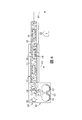
次に図3に示したブロック図を参照すると、付加材料の帯電したエアロゾル308を基板318へと堆積させるときに交差する付加材料取り扱い部分301と基板取り扱い部分311とを備える典型的な付加堆積システム300が示されている。材料取り扱い部分301は、帯電した付加材料を選択的に帯電させられて移動する基板へと向けるチャネルの通路を備える。通路またはチャネルの開口が、帯電したエアロゾルと基板表面層の選択された領域との間の静電位により、帯電した付加材料を静電力によって引き出し、基板表面層の領域へと堆積させることを可能にする。未堆積の材料、すなわち基板表面層の選択された部分へと引き付けられることがなかった帯電した付加材料を、付加材料取り扱い部分301へと再び再循環させ、あるいは再利用することができる。
Referring now to the block diagram shown in FIG. 3, a typical additive deposition system comprising an additive
フィラメント伸長式霧化器302が、システム300の付加材料取り扱い部分301に備えられている。フィラメント伸長式霧化器302は、基板表面層312へと堆積させるべき付加材料のエアロゾルを生成するために用いられる。フィラメント伸長式霧化器302は、反対向きに回転する1対のローラを使用し、付加材料の流体フィラメントをローラの下流側の離れていく表面の間で引き延ばす。フィラメントは、毛管破壊点まで引き伸ばされ、その時点で、各々の流体フィラメントの一部分が壊れ、付加材料の液滴のエアロゾルとなる。
A
フィラメント伸長式霧化器302を使用することで、非ニュートン性を呈する流体および材料を霧化させることができる。非ニュートン流体は、霧化させた流体材料のエアロゾルを生成するためにフィラメントを従来からのスプレー発生装置の能力を超えて引き伸ばすことを必要とする流体の引き伸ばされたフィラメントにおいて生じる伸長粘稠化ゆえに、霧化させることが困難であり得る。非ニュートン流体に加えて、流体伸長式霧化器は、ニュートン流体においてもエアロゾルを生成するために使用することができる。
The
次いで、エアロゾルを、エアロゾルサイズ選択装置または方法304によって、液滴のサイズまたは他の物理的パラメータにもとづいてフィルタ処理することができる。生成されたエアロゾルのサイズまたは他の物理的パラメータの選択304を、フィルタ、慣性衝突装置、あるいは所定の限界の外側の物理的パラメータを有する液滴を排除することができる他の装置または方法によって、行うことができる。慣性衝突装置は、エアロゾルの液滴の流れの中に配置され、鋭い角などの形状を備えており、液滴は、下流へと進むために、そのような形状の周りを流れなければならない。衝突装置の形状によって設定されるしきい値を上回る運動量を有する液滴は、周りを流れるよりもむしろ衝突装置の形状に衝突し、流れから排除される。液滴の運動量は、液滴の速度および質量の関数であり、衝突装置が所定のサイズおよび重量パラメータの外側の液滴を排除することを可能にする。
The aerosol can then be filtered by the aerosol size selection device or
エアロゾルは、基板312への堆積のための準備において帯電306させられる。エアロゾルは、エアロゾル帯電装置によって帯電306させられる。エアロゾル帯電装置は、コロナが封じ込まれている領域、イオン電流が流れている領域、または液滴からの電子の放出を喚起する電離放射線を生成して、エアロゾルの液滴を所望の第1の極性へと帯電させることができる。エアロゾルの帯電は、基板表面層312の一律な帯電とは反対の極性であってよく、これにより、帯電したエアロゾルは、基板表面層の反対に帯電させられた部分に引き付けられる。
The aerosol is charged 306 in preparation for deposition on the
ひとたび帯電させられると、エアロゾル308は、付加材料を堆積させるために、選択的に帯電させられた基板表面層318の表面の上方を平行に案内され、あるいは通過させられる。反対に帯電したエアロゾルおよび基板表面層の各部分は、静電位ゆえに互いに引き付け合う。静電位が、基板表面層の選択された領域へと堆積するようにエアロゾルを駆動する静電力を生む。付加材料の帯電したエアロゾルを、気流または他の方法によって通路またはチャネルを通って案内することができる。通路またはチャネルの開口が、帯電したエアロゾルの液滴が定められた領域においてのみ基板表面層の選択された部分と静電的に相互作用し、静電位および結果としての静電力を両者の間に生むことを可能にする。静電力により、付加材料の帯電したエアロゾルの一部が開口を通って通路またはチャネルから出て、基板表面層へと選択的に堆積する。
Once charged, the
未堆積の帯電したエアロゾルを、随意により、後の付加堆積プロセスにおける使用のために、再びフィラメント伸長式霧化器302へと再循環310させることができる。このやり方で、基板へと堆積した付加材料だけが実質的に使用され、したがって高い効率の付加プロセスがもたらされる。余分な未堆積の付加材料は、付加材料取り扱い部分301を通って再びフィラメント伸長式霧化器へと導かれる。次いで、流体付加材料は、さらなるエアロゾル生成プロセスを被ることができる。
The undeposited charged aerosol can optionally be recycled 310 back to the
付加堆積システム300の基板取り扱い部分311は、付加材料の選択的な堆積を促進するために、基板表面層312を一様に帯電させ、帯電を選択的に変化させることができる。基板表面層312を、最初に、帯電したエアロゾル308の第1の極性と同様または反対の極性の一様な帯電314で覆うことができる。ブランケット帯電装置を、基板表面層312を帯電させるために使用することができる。
The
ひとたび帯電で覆われると、帯電の少なくとも一部が選択的に変更316される。イオノグラフィック印刷ヘッドあるいは他の適切な装置または設備を、基板表面層の帯電を選択的に変更するために使用することができる。基板表面層の帯電の選択的な変更は、表面について電荷中性の領域、第1の極性と同様に帯電した領域、または第1の極性と反対に帯電した領域を生む。基板表面層のうちの中性または同様に帯電した部分は、帯電したエアロゾルを引き付けることがなく、これらの場所における付加材料の堆積が阻止または防止される。 Once covered with a charge, at least a portion of the charge is selectively modified 316. An ionographic printhead or other suitable device or equipment can be used to selectively modify the charging of the substrate surface layer. The selective modification of the charging of the substrate surface layer results in areas of charge neutrality on the surface, areas of similar charge to the first polarity, or areas of opposite charge to the first polarity. Neutral or similarly charged portions of the substrate surface layer do not attract the charged aerosol and the deposition of additional material at these locations is prevented or prevented.
基板表面層の帯電の一部を選択的に変更した後で、基板は、帯電したエアロゾルの案内構造を過ぎて運搬318される。帯電したエアロゾルの液滴が、帯電したエアロゾルと基板表面層の選択された領域との間の静電位によって引き起こされる静電力によって基板表面層へと選択的に堆積させられる。ひとたび堆積させられると、付加材料は、冷えて固まることができる。 After selectively altering a portion of the charge on the substrate surface layer, the substrate is transported 318 past the charged aerosol guide structure. The charged aerosol droplets are selectively deposited on the substrate surface layer by electrostatic forces caused by electrostatic potential between the charged aerosol and selected areas of the substrate surface layer. Once deposited, the add-on material can cool and set.
基板を、さらなる付加堆積工程に曝すこともできる。支持材料を、堆積させられた付加材料の間に適用320して、新たな平らな基板層表面を生成することができる。上述のように、支持材料を、現在の基板表面層の全体に施し、選択的に堆積させられた付加材料の周囲で平らにすることで、次の付加堆積プロセスのための新たな基板層表面を形成することができる。結果は、基板層表面を形成する付加材料および支持材料の平滑な連続した層、すなわち付加材料と元の基板層によって支持された付加材料とからなる全体構造である。 The substrate can also be exposed to additional additive deposition steps. Support material can be applied 320 between the deposited additional materials to create a new planar substrate layer surface. As described above, the support material is applied over the current substrate surface layer and flattened around the selectively deposited additive material to provide a new substrate layer surface for the next additive deposition process. Can be formed. The result is a smooth continuous layer of add-on material and support material that forms the substrate layer surface, i.e. an overall structure of add-on material and add-on material supported by the original substrate layer.
繰り返しの付加堆積プロセスを実行すべき場合、選択的に堆積させられた付加材料の先行の層を、多層構造を形成すべく次の付加材料層の付着および接着を助けるために、半流動体の状態に保つことができる。一例として、付加材料の連続する選択的な堆積の各々が、先行して堆積させられた材料に接着するように、プロセスの全体を加熱された環境において完了させることができる。 If repeated iterative deposition processes are to be performed, the preceding layer of selectively deposited additive material may be replaced with a semi-fluidic layer to assist in the deposition and adhesion of the next additional material layer to form a multilayer structure. Can be kept in a state. As an example, the entire process can be completed in a heated environment such that each successive selective deposition of the additional material adheres to the previously deposited material.
堆積させられた付加材料および/または基板表面層に残余の帯電があれば、スコロトロンによる事前の帯電工程において同時に中和322させることができる。あるいは、残余の帯電の中和を、スコロトロンによる事前の帯電工程の前に、別の工程として行うことができる。表面が、今や再び付加堆積システム300の基板取り扱い部分311を通って移動する。このプロセスを、必要に応じた回数だけ繰り返し、選択的に適用された付加材料の構造体またはマトリクスを生み出すことができる。層を生成するために、基板の運搬318は、基板を鉛直軸において移動させることによって、帯電したエアロゾルの堆積と基板層表面との間に一定かつ不変の隔たりを保つことを含むことができる。あるいは、同じ隔たりを維持するために、帯電したエアロゾルの堆積を鉛直方向に移動させることができる。ひとたび所望の構造体またはマトリクスが完成すると、必要または所望であれば、溶媒による除去、機械的な除去、または熱による除去を含むいくつかの異なるプロセスを使用して、支持材料を付加材料から分離させることができる。
Any residual charge on the deposited additive material and/or substrate surface layer can be simultaneously neutralized 322 in a previous charging step with a scorotron. Alternatively, the neutralization of the residual charge can be performed as a separate step before the previous charging step with the scorotron. The surface now moves again through the
図4が、本発明の実施形態による付加堆積システム400の典型的な付加材料準備部分401である。システム400の準備部分401において、付加材料のエアロゾル406が、フィラメント伸長式霧化器402を使用して形成される。付加材料のエアロゾル422は、開口430を通じた基板への堆積の準備において、帯電させられる。流体の形態の付加材料が、外部または内部のいずれかからフィラメント伸長式霧化器402へと導入される。反対向きに回転する1対のローラ404が、流体付加材料をとらえ、ローラ404の互いに遠ざかる下流の表面の間で付加材料のフィラメントを引き伸ばす。流体フィラメントがローラ404の間で引き伸ばされるにつれて、流体フィラメントは、不安定の点、すなわち毛管破壊点に達する。毛管破壊点において、各々の流体フィラメントの少なくとも一部分が壊れ、付加流体の液滴406のエアロゾルとなる。導入される気流408を、形成されたエアロゾルをシステム400の付加材料準備部分401を通って案内するために使用することができる。気流408を、フィラメント伸長式霧化器402のローラ404の回転によって生じさせることができ、あるいは外部の供給源などの他の手段によって生成することができる。
FIG. 4 is an exemplary additive material preparation portion 401 of an
図4に示されるようにフィラメント伸長式霧化器402を縦向きにすることで、フィラメント伸長式霧化器402によって形成されるエアロゾル406を、液滴のサイズおよび/または重量にもとづいてフィルタ処理することができる。形成されたエアロゾル406の液滴への重力を、サイズ超過および/または重量超過の液滴が部分401を通ってさらに進むことを防止するために使用することができる。気流408に対するフィラメント伸長式霧化器402の鉛直高さの変更を、所望のサイズおよび/または重量の液滴がフィラメント伸長式霧化器402を出て部分401を通って通路410へと移動を続けることを選択的に許すために、使用することができる。
By orienting the filament elongate atomizer 402 in a vertical orientation as shown in FIG. 4, the aerosol 406 formed by the filament elongate atomizer 402 is filtered based on droplet size and/or weight. can do. Gravity on the formed droplets of aerosol 406 can be used to prevent oversized and/or overweight droplets from further advancing through portion 401. Altering the vertical height of the filament extender atomizer 402 relative to the
通路410が、生成されたエアロゾルをフィラメント伸長式霧化器402からシステム400の付加材料取り扱い部分401を通って案内する。通路410は、帯電したエアロゾルと選択的に帯電が変更された基板表面層との間の静電相互作用にもとづく帯電した付加材料の基板表面層の選択された部分への堆積を促進するために、生成されたエアロゾルの流れを運ばれる基板に平行に、運ばれる基板の直近に案内するように配置される。
A
液滴セレクタ412を、付加材料取り扱い部分401の通路410の内部に配置することができる。液滴セレクタ412は、一式の所望のパラメータの外側のサイズおよび重量などの物理的パラメータを有する液滴を選択的に除去または排除することができる。排除された液滴を、後の使用のために再びフィラメント伸長式霧化器402へと再循環414させることができる。図4に示される実施形態において、液滴セレクタ412は、流れている形成されたエアロゾルの流れの中に配置された慣性衝突装置である。衝突装置は、エアロゾルの液滴をそれらの運動量にもとづいて選択的にフィルタ処理するための形状を備えている。この形状を使用して、所定および/または所望の物理的パラメータの範囲の外側の液滴が通路410を通って進み続けることが阻止される。
エアロゾル帯電装置420が、通過するエアロゾルの液滴を帯電させる。帯電装置420は、基板表面層への堆積の準備において、エアロゾルの液滴に帯電を生じさせる。帯電装置420は、エアロゾルの液滴が通過するコロナが封じ込まれている領域、イオン電流が流れている領域、または電離放射線を生成することができる。これは、液滴からの電子の放出を生じさせ、液滴を所望の極性へと帯電させる。帯電したエアロゾルの液滴422は、通路410を通り、堆積用開口430を横切って移動を続ける。
The
帯電したエアロゾル422が堆積用開口430を通り過ぎるとき、帯電したエアロゾルの一部が、帯電したエアロゾル422と基板表面層との間の静電位によって引き起こされる静電力ゆえに、下方を通過する基板表面層へと開口430を通って引き付けられ、堆積する。通路を通って移動を続ける余分または残余の帯電したエアロゾル422を、再びシステム400へと再循環414させることができる。
As the charged
図5は、付加堆積システム400の典型的な基板部分501を示している。この部分において、基板502の全体を一様に帯電させることができ、その後に基板502の層表面の帯電の一部を、選択的に変更することができる。基板502が堆積通路の開口430の直下を通過するとき、帯電したエアロゾルの液滴422が、基板502の層表面と帯電したエアロゾル422との間の静電位によって引き起こされる静電力ゆえに、基板502の層表面の選択された領域へと引き付けられて堆積する。静電力は、帯電したエアロゾル422の一部を堆積通路の開口430から基板502の層表面の選択された領域へと駆動する。残りの帯電したエアロゾルは、堆積通路410を通って移動を続け、再利用または廃棄される。帯電したエアロゾル422は、基板の表面の反対に帯電させられた部分へと引き付けられる。ギャップ514が、付加材料423の堆積させられた部分の間に生じるが、基板層表面を覆う支持材料および付加材料の平滑かつ連続的な層を生み出すために、支持材料530で埋められる。次いで、帯電が基板および付加材料から実質的に中和され、さらなる付加材料堆積プロセスのために付加堆積システム400へと送り込むことができる新たな静電的に中性な基板層表面が生み出される。基板502は、基板運搬システム506によってシステム400を通って運ばれる。
FIG. 5 illustrates an
一様かつ全面的な帯電を、ブランケット帯電装置504によって基板502の層表面を横断して生じさせることができる。図5に示される典型的な実施形態において、基板は、負の帯電で覆われる。典型的な実施形態においては、スコロトロンを、基板層表面を横断する全面的な帯電を生じさせるために使用することができる。スコロトロンは、コロナ放電を生じさせて電荷を通過する基板に向かって加速させることによって基板層表面を帯電させ、表面の電荷密度によって表面の電位がスコロトロン格子の電位に等しくなるまで基板表面層を帯電させる。コロナ放電を、金属壁のシリンダの内部の細いワイヤに高い電圧を置くことによって形成することができる。このようにして生み出される強い電界が、空気などの周囲の気体を電離させる。基板が形成された荷電粒子の雲を通過するとき、基板層表面が、その放出された粒子の極性へと帯電させられる。スコロトロンは、基板層表面を、以前の帯電の状態にかかわらずに一様な電荷密度へと帯電させることができ、したがってさらなる付加堆積プロセスを行う前に、支持材料および付加材料からなる新たな基板層表面の残余の電荷を減らしたり、実質的に中和したりする必要を、なくすことができる。
A uniform and global charging can be produced across the layer surface of
ひとたび基板502の層表面が連続的かつ等しい電荷で覆われると、帯電の一部を、入力にもとづいて選択的帯電装置510によって選択的に変更することができる。入力は、ユーザ、コンピュータプログラム、などからもたらされてよく、装置510によって実行される選択的な帯電の変更のパターンに関する指示を含む。図示の実施形態において、選択的帯電装置510は、イオノグラフィック印刷ヘッドである。イオノグラフィック印刷ヘッドは、帯電した基板の極性と反対の極性を有するイオンの流れを案内する(あるいは、格子を使用して加速させる)。放射された反対に帯電したイオンが、基板層表面の局所領域を中和し、あるいは反対に帯電させる。このやり方で、イオノグラフィック印刷ヘッドは、パターン、コンピュータ制御指示、などの入力にもとづいて中和、反対の帯電、または選択的なやり方での帯電を行うことができる。イオノグラフィック印刷ヘッド510を、基板502の移動に対して垂直に、直線的なやり方で基板502の表面を横切って移動させることができ、各回の通過後に基板502をイオノグラフィック印刷ヘッド510の幅だけ前進させることができる。イオノグラフィック印刷ヘッド510の直線移動は、基板502の移動との組み合わせにおいて、基板502の表面全体に選択的に帯電させられた部分の2次元パターンを形成する。
Once the layer surface of the
あるいは、イオノグラフィック印刷ヘッドのアレイまたは他のイオン堆積装置を、配置することができる。このやり方で、アレイの各回の通過によって覆われる基板502の層表面の量を、増やすことができる。あるいは、アレイは、基板502の幅以上の距離に及ぶことができ、これは、アレイを固定し、その下方で基板502を連続的または段階的なやり方で前進させることを、可能にすると考えられる。
Alternatively, an array of ionographic printheads or other ion deposition device can be arranged. In this way, the amount of layer surface of
イオノグラフィック印刷ヘッド510が基板502の表面層の帯電の少なくとも一部を選択的に変更した後で、基板502は、基板運搬システム506によって堆積用開口430の下方を運ばれる。帯電したエアロゾル422が通路410を通って流れ、堆積用開口430を横切るとき、帯電したエアロゾル422の一部が、基板502の層表面の反対に帯電した領域512へと引き付けられる。図示の例では、基板502の層表面の反対に帯電した部分512は、基板502の層表面のうちの一律な帯電が選択的に取り除かれたり、あるいは反対に帯電させられたりしていない部分である。
After the
基板502の表面のうちの帯電が中性または反対の帯電状態へと選択的に変えられた部分は、選択的に堆積させられた帯電した付加材料423の間のギャップ514を形成する。支持材料530が、基板502の層表面および堆積させられた付加材料422を横断して堆積させられ、ギャップ514を満たす。ドクターブレード534が、基板502の表面から所定の距離だけ離して配置され、選択的に堆積させられた付加材料422および支持材料530の表面を滑らかかつ平らにする。ひとたび基板502の層表面が堆積させられた付加材料423および支持材料530で覆われると、残る帯電または残余の帯電を、材料422および530ならびに基板502から実質的に低減または中和することができる。
The portions of the surface of the
上述のように、基板502は、繰り返しの付加材料堆積プロセスに曝されてよく、あるいは付加材料は、必要であれば基板へと固着できてよい。支持材料530は、硬化のプロセスの一部として基板502へと接着されてよく、あるいは堆積させられて硬化した付加材料の物体を残して取り除かれてよい。
As mentioned above, the
基板運搬システム506は、基板502の平面内の水平方向および基板502に垂直な鉛直方向に基板を移動させることができる。図示の実施形態においては、基板502を、3つの軸に沿ってシステム506によって移動させることができる。選択的帯電装置510が基板502の層表面を横切る軸にて移動させられる例においては、基板運搬システム506が、選択的帯電装置510の各回の通過後に刻みまたは段階的なやり方で基板502を移動させることができる。ひとたび基板502の層表面の帯電の変更が完了すると、基板運搬システムは、選択的に堆積させられる付加材料の新たな層を生成するための水平面における移動を繰り返す前に、鉛直軸にて基板502を移動させることができる。選択的帯電装置510または装置510のアレイが不動である別の例においては、基板502を、所望の帯電除去パターンを完成させるために、2つ以上の軸にて移動させることができる。
The
付加堆積システム400の基板部分501の種々の構成要素を、基板502が構成要素504、510、および530の下方を順に移動させられるように配置することができる。このやり方で、基板502を、システム400によって連続的に処理することができる。
The various components of
システム400による付加材料堆積プロセスの繰り返しを、付加材料を材料の3次元のマトリクスに積み重ねるために使用することができる。繰り返しの付加材料堆積プロセスによって、高分解能の3次元物体が生成される。付加堆積プロセスの分解能は、選択的帯電除去装置510の細かさおよび精度にもとづいて変化し得る。分解能は、堆積させられる付加材料の選択的な厚さによってさらに高められる。帯電したエアロゾル422と反対に帯電した基板502との間の静電位が大きいほど、静電位の大きさに依存して基板層表面の反対に帯電した領域を中和するためにさらなる帯電したエアロゾルが必要となり得るため、基板502上にエアロゾル化させた付加材料のより大きな凝集をもたらすことができる。上述のように、支持材料530を仕上げ処理において除去し、堆積させられた付加材料で形成された中実な3次元の物体を露出させることができる。
Repeating the additive material deposition process by
Claims (9)
前記生成された付加材料のエアロゾルを第1の極性に帯電させるためのエアロゾル帯電装置と、
基板層表面の部分の帯電を選択的に変更するための選択的帯電装置と
を備えており、
前記帯電させられた付加材料のエアロゾルが、該帯電させられた付加材料のエアロゾルと帯電が変更された前記基板の部分との間の静電位に起因する静電力によって、前記帯電が変更された前記基板の部分へと選択的に堆積させられ、
前記選択的に堆積させられた帯電させられたエアロゾルの周囲に支持材料を堆積させるための支持材料堆積装置
をさらに備える、付加材料の堆積システムであって、
前記システムは、三次元の物体を形成するために、前記エアロゾルを生成し、前記エアロゾルを帯電させ、前記基板層表面を帯電させ、前記帯電させられたエアロゾルを堆積させ、前記支持材料を堆積させることを繰り返す、前記付加材料の堆積システム。 An aerosol generating device configured to generate an aerosol of the additional material;
An aerosol charging device for charging the generated additional material aerosol to a first polarity;
And a selective charging device for selectively changing the charging on the surface of the substrate layer,
The charged charge aerosol of the additive material is changed in charge by an electrostatic force resulting from an electrostatic potential between the charged additive material aerosol and a portion of the substrate where the charge is changed. Selectively deposited onto a portion of the substrate,
A deposition system for additional material, further comprising: a support material deposition apparatus for depositing a support material around the selectively deposited charged aerosol.
The system produces the aerosol, charges the aerosol, charges the substrate layer surface, deposits the charged aerosol, and deposits the support material to form a three-dimensional object. The deposition system of the additional material, which is repeated.
をさらに備える請求項1に記載の付加材料の堆積システム。 The additive material deposition system according to claim 1, further comprising: a substrate charging device configured to uniformly charge the surface of the substrate layer by charging having a second polarity.
をさらに備えており、
前記エアロゾル堆積通路は、前記帯電させられたエアロゾルを該エアロゾル堆積通路に設けられた開口を横切って前記基板に平行に案内するように構成され、前記帯電させられたエアロゾルの少なくとも一部が、前記静電力によって前記開口のすぐ近くに導かれ、前記基板層表面の帯電させられた部分へと堆積させられる、請求項1に記載の付加材料の堆積システム。 Further comprising an aerosol deposition passageway located proximate to the substrate,
The aerosol deposition passage is configured to guide the charged aerosol parallel to the substrate across an opening provided in the aerosol deposition passage, wherein at least a portion of the charged aerosol is The additive material deposition system of claim 1, wherein the additive material is directed in the immediate vicinity of the opening by electrostatic forces and deposited on a charged portion of the substrate layer surface.
Applications Claiming Priority (2)
| Application Number | Priority Date | Filing Date | Title |
|---|---|---|---|
| US15/001,408 US10500784B2 (en) | 2016-01-20 | 2016-01-20 | Additive deposition system and method |
| US15/001,408 | 2016-01-20 |
Publications (3)
| Publication Number | Publication Date |
|---|---|
| JP2017128116A JP2017128116A (en) | 2017-07-27 |
| JP2017128116A5 JP2017128116A5 (en) | 2020-02-27 |
| JP6749849B2 true JP6749849B2 (en) | 2020-09-02 |
Family
ID=57796214
Family Applications (1)
| Application Number | Title | Priority Date | Filing Date |
|---|---|---|---|
| JP2017003656A Active JP6749849B2 (en) | 2016-01-20 | 2017-01-12 | Additive deposition system and method |
Country Status (6)
| Country | Link |
|---|---|
| US (1) | US10500784B2 (en) |
| EP (1) | EP3196002B1 (en) |
| JP (1) | JP6749849B2 (en) |
| KR (1) | KR102481039B1 (en) |
| CN (1) | CN106985378B (en) |
| TW (1) | TWI707769B (en) |
Families Citing this family (9)
| Publication number | Priority date | Publication date | Assignee | Title |
|---|---|---|---|---|
| US9757747B2 (en) | 2014-05-27 | 2017-09-12 | Palo Alto Research Center Incorporated | Methods and systems for creating aerosols |
| US11724448B2 (en) * | 2017-07-17 | 2023-08-15 | Hewlett-Packard Development Company, L.P. | Disguising color in 3D object formation |
| US10493483B2 (en) | 2017-07-17 | 2019-12-03 | Palo Alto Research Center Incorporated | Central fed roller for filament extension atomizer |
| US10464094B2 (en) | 2017-07-31 | 2019-11-05 | Palo Alto Research Center Incorporated | Pressure induced surface wetting for enhanced spreading and controlled filament size |
| US10919215B2 (en) * | 2017-08-22 | 2021-02-16 | Palo Alto Research Center Incorporated | Electrostatic polymer aerosol deposition and fusing of solid particles for three-dimensional printing |
| US10786946B2 (en) | 2017-09-13 | 2020-09-29 | Thermwood Corporation | Apparatus and methods for compressing material during additive manufacturing |
| DE102018107585B3 (en) * | 2018-03-29 | 2019-03-28 | Universität Rostock | Device for producing 3D printed drug delivery systems with drug depots, and methods for manufacturing 3D printed drug delivery systems |
| US20220380928A1 (en) * | 2021-05-29 | 2022-12-01 | Nissan North America, Inc. | Method and system of powder coating a vehicle component |
| US11909052B2 (en) | 2021-06-30 | 2024-02-20 | Xerox Corporation | Fabrication of membrane electrode assembly with filament extension atomizer spray |
Family Cites Families (75)
| Publication number | Priority date | Publication date | Assignee | Title |
|---|---|---|---|---|
| US2291046A (en) | 1942-07-28 | Arrangement for burning liquid fuel | ||
| US2551582A (en) * | 1943-08-27 | 1951-05-08 | Chester F Carlson | Method of printing and developing solvent images |
| FR1035235A (en) | 1951-04-09 | 1953-08-19 | Rodanet & Cie Ets | Improvements to paint rollers, automatic feed and hand |
| US3052213A (en) | 1958-12-17 | 1962-09-04 | Ibm | Electrostatic printer apparatus for printing with liquid ink |
| DE1302344B (en) | 1961-02-06 | |||
| BE616914A (en) | 1961-04-26 | |||
| CH413018A (en) | 1963-04-30 | 1966-05-15 | Du Pont | Thermoelectric generator |
| US3926114A (en) | 1967-06-30 | 1975-12-16 | Walter E S Matuschke | Rotary lithographic printing press with ink and dampening fluid separator |
| US3702258A (en) | 1969-03-05 | 1972-11-07 | Eastman Kodak Co | Web treatment method |
| US3626833A (en) | 1969-06-09 | 1971-12-14 | Addressograph Multigraph | Liquid developing apparatus |
| US3977323A (en) | 1971-12-17 | 1976-08-31 | Electroprint, Inc. | Electrostatic printing system and method using ions and liquid aerosol toners |
| US3649829A (en) | 1970-10-06 | 1972-03-14 | Atomic Energy Commission | Laminar flow cell |
| US3779166A (en) | 1970-12-28 | 1973-12-18 | Electroprint Inc | Electrostatic printing system and method using ions and toner particles |
| US3717875A (en) | 1971-05-04 | 1973-02-20 | Little Inc A | Method and apparatus for directing the flow of liquid droplets in a stream and instruments incorporating the same |
| US3797926A (en) | 1971-08-27 | 1974-03-19 | Horizons Inc | Imaging system employing ions |
| US3873025A (en) * | 1974-05-06 | 1975-03-25 | Stora Kopparbergs Bergslags Ab | Method and apparatus for atomizing a liquid medium and for spraying the atomized liquid medium in a predetermined direction |
| US4034670A (en) | 1975-03-24 | 1977-07-12 | Rockwell International Corporation | Dampening device for lithographic printing press |
| US4217062A (en) | 1978-02-27 | 1980-08-12 | Mile Lipovac | Paint feeding apparatus in combination with a fountain type paint roller |
| US4222059A (en) | 1978-12-18 | 1980-09-09 | Xerox Corporation | Ink jet multiple field electrostatic lens |
| US4384296A (en) | 1981-04-24 | 1983-05-17 | Xerox Corporation | Linear ink jet deflection method and apparatus |
| US4860652A (en) | 1986-05-24 | 1989-08-29 | Kabushikigaisha Tokyo Kikai Seisakusho | Mesh roller for planography |
| DE3822692C2 (en) | 1988-07-05 | 1996-02-15 | Kochsmeier Hans Hermann | Anilox roller in an order work of a printing press |
| CA2006227C (en) | 1989-04-27 | 1995-07-18 | Goss Graphic Systems, Inc. | Hydrophobic and oleophilic microporous inking rollers |
| US5127325A (en) | 1989-04-27 | 1992-07-07 | Rockwell International Corporation | Hydrophobic and oleophilic microporous inking rollers |
| DK0420488T3 (en) | 1989-09-25 | 1993-08-30 | Schneider Usa Inc | Multilayer extrusion as a method for preparing angioplasty balloons |
| US5103763A (en) * | 1989-12-08 | 1992-04-14 | International Business Machines Corporation | Apparatus for formation and electrostatic deposition of charged droplets |
| US5204697A (en) | 1990-09-04 | 1993-04-20 | Xerox Corporation | Ionographic functional color printer based on Traveling Cloud Development |
| DE4036661C1 (en) | 1990-11-17 | 1992-06-17 | Man Roland Druckmaschinen Ag, 6050 Offenbach, De | |
| US5207158A (en) | 1991-02-19 | 1993-05-04 | Rockwell International | Long lived, variable-delivery ink metering method, system and roller for keyless lithography |
| GB9200936D0 (en) | 1992-01-16 | 1992-03-11 | Sprayforming Dev Ltd | Improvements in the processing of metals and alloys |
| US5314119A (en) * | 1992-04-20 | 1994-05-24 | Latanick Equipment, Inc. | Method and apparatus for applying thin coatings of fluid droplets |
| US5609919A (en) | 1994-04-21 | 1997-03-11 | Altamat Inc. | Method for producing droplets |
| US5746844A (en) | 1995-09-08 | 1998-05-05 | Aeroquip Corporation | Method and apparatus for creating a free-form three-dimensional article using a layer-by-layer deposition of molten metal and using a stress-reducing annealing process on the deposited metal |
| US6399143B1 (en) * | 1996-04-09 | 2002-06-04 | Delsys Pharmaceutical Corporation | Method for clamping and electrostatically coating a substrate |
| US6506438B2 (en) | 1998-12-15 | 2003-01-14 | E Ink Corporation | Method for printing of transistor arrays on plastic substrates |
| CA2389557C (en) | 1999-11-26 | 2009-09-22 | Unilever Plc | Applicator for applying a fluid to a surface and method of applying a fluid to a surface |
| US6622335B1 (en) | 2000-03-29 | 2003-09-23 | Lam Research Corporation | Drip manifold for uniform chemical delivery |
| US6576861B2 (en) | 2000-07-25 | 2003-06-10 | The Research Foundation Of State University Of New York | Method and apparatus for fine feature spray deposition |
| DE10108717C1 (en) | 2001-02-23 | 2002-07-11 | Bosch Gmbh Robert | Apparatus for removing electric charge from a plastic sheet, paper web or polymer fibers, comprises a plasma generator producing plasma containing charged particles and rollers which feed sheet through the region containing plasma |
| US20070194157A1 (en) * | 2002-08-06 | 2007-08-23 | Clean Earth Technologies, Llc | Method and apparatus for high transfer efficiency electrostatic spray |
| US20040050701A1 (en) | 2002-09-13 | 2004-03-18 | Mcentee John Francis | Electrostatically guiding ionized droplets in chemical array fabrication |
| US20060068082A1 (en) | 2002-09-25 | 2006-03-30 | Koninklijke Philips Electronics N.V. | Method of electrostatic deposition |
| KR100519343B1 (en) | 2003-07-02 | 2005-10-07 | 엘지전자 주식회사 | wearable cooler |
| US7083830B2 (en) | 2003-10-02 | 2006-08-01 | E. I. Dupont De Nemours And Company | Electrostatically-assisted high-speed rotary application process for the production of special effect base coat/clear coat two-layer coatings |
| EP1625893A1 (en) | 2004-08-10 | 2006-02-15 | Konica Minolta Photo Imaging, Inc. | Spray coating method, spray coating device and inkjet recording sheet |
| US7938341B2 (en) | 2004-12-13 | 2011-05-10 | Optomec Design Company | Miniature aerosol jet and aerosol jet array |
| DE102005022308B4 (en) | 2005-05-13 | 2007-03-22 | Eos Gmbh Electro Optical Systems | Apparatus and method for manufacturing a three-dimensional object with a heated powder coating material build-up material |
| WO2008063241A1 (en) * | 2006-11-22 | 2008-05-29 | Entegris, Inc. | Diamond like carbon coating of substrate housing |
| JP2008227178A (en) | 2007-03-13 | 2008-09-25 | Sumitomo Chemical Co Ltd | Thermoelectric conversion module and substrate therefor |
| TWI338390B (en) | 2007-07-12 | 2011-03-01 | Ind Tech Res Inst | Flexible thermoelectric device and manufacturing method thereof |
| DE102007034877A1 (en) * | 2007-07-24 | 2009-01-29 | Schmid Rhyner Ag | Method and device for applying plastic coatings |
| TWI482662B (en) | 2007-08-30 | 2015-05-01 | Optomec Inc | Mechanically integrated and closely coupled print head and mist source |
| US20090155732A1 (en) | 2007-12-13 | 2009-06-18 | Palo Alto Research Center Incorporated | Method for Patterning Using Phase-Change Material |
| TW200933940A (en) | 2007-12-28 | 2009-08-01 | Basf Se | Extrusion process for preparing improved thermoelectric materials |
| CN103872002B (en) | 2008-03-05 | 2017-03-01 | 伊利诺伊大学评议会 | Stretchable and foldable electronic device |
| EP2131406A1 (en) | 2008-06-02 | 2009-12-09 | Nederlandse Organisatie voor toegepast- natuurwetenschappelijk onderzoek TNO | A method for manufacturing a thermoelectric generator, a wearable thermoelectric generator and a garment comprising the same |
| US9346021B2 (en) | 2008-12-02 | 2016-05-24 | Membrane Distillation Desalination Ltd., Co. | Composite membranes for membrane distillation and related methods of manufacture |
| US9163883B2 (en) | 2009-03-06 | 2015-10-20 | Kevlin Thermal Technologies, Inc. | Flexible thermal ground plane and manufacturing the same |
| JP5573046B2 (en) | 2009-08-24 | 2014-08-20 | 富士通株式会社 | Film forming apparatus and film forming method |
| US20110150036A1 (en) | 2009-12-21 | 2011-06-23 | Electronics And Telecommunications Research Institute | Flexible thermoelectric generator, wireless sensor node including the same and method of manufacturing the same |
| EP2498310A3 (en) | 2011-03-11 | 2013-12-11 | Imec | Thermoelectric textile |
| US8720370B2 (en) | 2011-04-07 | 2014-05-13 | Dynamic Micro System Semiconductor Equipment GmbH | Methods and apparatuses for roll-on coating |
| JP5656295B2 (en) | 2011-04-22 | 2015-01-21 | パナソニックIpマネジメント株式会社 | Thermoelectric conversion module and manufacturing method thereof |
| US9021948B2 (en) | 2011-04-27 | 2015-05-05 | Xerox Corporation | Environmental control subsystem for a variable data lithographic apparatus |
| US20130087180A1 (en) | 2011-10-10 | 2013-04-11 | Perpetua Power Source Technologies, Inc. | Wearable thermoelectric generator system |
| US9132645B2 (en) | 2012-11-29 | 2015-09-15 | Palo Alto Research Center Incorporated | Pulsating heat pipe spreader for ink jet printer |
| KR101545049B1 (en) * | 2013-09-13 | 2015-08-17 | 엔젯 주식회사 | System for coating using spray nozzle |
| KR101625714B1 (en) * | 2013-08-27 | 2016-05-30 | 엔젯 주식회사 | Apparatus for spray patterning using electrostatic force |
| US10016777B2 (en) | 2013-10-29 | 2018-07-10 | Palo Alto Research Center Incorporated | Methods and systems for creating aerosols |
| US9433957B2 (en) | 2014-01-08 | 2016-09-06 | United Technologies Corporation | Cold spray systems with in-situ powder manufacturing |
| US20150197063A1 (en) | 2014-01-12 | 2015-07-16 | Zohar SHINAR | Device, method, and system of three-dimensional printing |
| KR20150128499A (en) * | 2014-05-10 | 2015-11-18 | 성균관대학교산학협력단 | 3D printing method using particles coated with ionic copolymer |
| US9694379B2 (en) | 2014-05-30 | 2017-07-04 | The Procter & Gamble Company | Customizable apparatus and method for transporting and depositing fluids |
| EP3256308B1 (en) | 2015-02-10 | 2022-12-21 | Optomec, Inc. | Fabrication of three-dimensional structures by in-flight curing of aerosols |
| US10400119B2 (en) | 2015-05-07 | 2019-09-03 | Ehsan Toyserkani | Method and apparatus for aerosol-based three-dimensional (3D) printing of flexible graphene electronic devices |
-
2016
- 2016-01-20 US US15/001,408 patent/US10500784B2/en not_active Expired - Fee Related
-
2017
- 2017-01-05 TW TW106100332A patent/TWI707769B/en active
- 2017-01-11 CN CN201710020713.8A patent/CN106985378B/en active Active
- 2017-01-11 KR KR1020170004043A patent/KR102481039B1/en active IP Right Grant
- 2017-01-12 EP EP17151223.9A patent/EP3196002B1/en active Active
- 2017-01-12 JP JP2017003656A patent/JP6749849B2/en active Active
Also Published As
| Publication number | Publication date |
|---|---|
| CN106985378B (en) | 2022-03-01 |
| EP3196002A1 (en) | 2017-07-26 |
| CN106985378A (en) | 2017-07-28 |
| US10500784B2 (en) | 2019-12-10 |
| EP3196002B1 (en) | 2020-08-19 |
| TW201805147A (en) | 2018-02-16 |
| KR102481039B1 (en) | 2022-12-27 |
| JP2017128116A (en) | 2017-07-27 |
| KR20170087407A (en) | 2017-07-28 |
| US20170203504A1 (en) | 2017-07-20 |
| TWI707769B (en) | 2020-10-21 |
Similar Documents
| Publication | Publication Date | Title |
|---|---|---|
| JP6749849B2 (en) | Additive deposition system and method | |
| JP6736487B2 (en) | Additive deposition system and method | |
| EP3362260B1 (en) | Method for the production of silicone elastomer parts having increased printing quality | |
| KR102267119B1 (en) | Spray charging and discharging system for polymer spray deposition device | |
| US11413813B2 (en) | Electrostatic polymer aerosol deposition and fusing of solid particles for three-dimensional printing | |
| EP3568247A1 (en) | Method and apparatus for continuously refreshing a recoater blade for additive manufacturing | |
| US20170216918A1 (en) | Methods and systems for fabrication using multi-material and precision alloy droplet jetting | |
| DE102016223244A1 (en) | Method and apparatus for generative manufacturing of a three-dimensional object and three-dimensional object | |
| US9988720B2 (en) | Charge transfer roller for use in an additive deposition system and process | |
| JP2022554199A (en) | Assembly and method for producing layers of particulate structural material with a 3D printer | |
| Johnson et al. | Polymer spray deposition: a novel aerosol-based, electrostatic digital deposition system for additive manufacturing | |
| Wei | Investigation of Hierarchical Fabrication Methods for High-Resolution Additive Manufacturing | |
| Michaelis et al. | Heat transfer manipulation for precision droplet manufacturing: simulation and experiment |
Legal Events
| Date | Code | Title | Description |
|---|---|---|---|
| RD03 | Notification of appointment of power of attorney |
Free format text: JAPANESE INTERMEDIATE CODE: A7423 Effective date: 20170124 |
|
| RD04 | Notification of resignation of power of attorney |
Free format text: JAPANESE INTERMEDIATE CODE: A7424 Effective date: 20170125 |
|
| A521 | Request for written amendment filed |
Free format text: JAPANESE INTERMEDIATE CODE: A523 Effective date: 20200114 |
|
| A621 | Written request for application examination |
Free format text: JAPANESE INTERMEDIATE CODE: A621 Effective date: 20200114 |
|
| A871 | Explanation of circumstances concerning accelerated examination |
Free format text: JAPANESE INTERMEDIATE CODE: A871 Effective date: 20200114 |
|
| A975 | Report on accelerated examination |
Free format text: JAPANESE INTERMEDIATE CODE: A971005 Effective date: 20200204 |
|
| A131 | Notification of reasons for refusal |
Free format text: JAPANESE INTERMEDIATE CODE: A131 Effective date: 20200330 |
|
| A521 | Request for written amendment filed |
Free format text: JAPANESE INTERMEDIATE CODE: A523 Effective date: 20200610 |
|
| TRDD | Decision of grant or rejection written | ||
| A01 | Written decision to grant a patent or to grant a registration (utility model) |
Free format text: JAPANESE INTERMEDIATE CODE: A01 Effective date: 20200713 |
|
| A61 | First payment of annual fees (during grant procedure) |
Free format text: JAPANESE INTERMEDIATE CODE: A61 Effective date: 20200812 |
|
| R150 | Certificate of patent or registration of utility model |
Ref document number: 6749849 Country of ref document: JP Free format text: JAPANESE INTERMEDIATE CODE: R150 |