JP6736388B2 - Image forming device - Google Patents
Image forming device Download PDFInfo
- Publication number
- JP6736388B2 JP6736388B2 JP2016133375A JP2016133375A JP6736388B2 JP 6736388 B2 JP6736388 B2 JP 6736388B2 JP 2016133375 A JP2016133375 A JP 2016133375A JP 2016133375 A JP2016133375 A JP 2016133375A JP 6736388 B2 JP6736388 B2 JP 6736388B2
- Authority
- JP
- Japan
- Prior art keywords
- photosensitive drum
- potential
- surface potential
- image
- voltage
- Prior art date
- Legal status (The legal status is an assumption and is not a legal conclusion. Google has not performed a legal analysis and makes no representation as to the accuracy of the status listed.)
- Active
Links
Images


Classifications
-
- G—PHYSICS
- G03—PHOTOGRAPHY; CINEMATOGRAPHY; ANALOGOUS TECHNIQUES USING WAVES OTHER THAN OPTICAL WAVES; ELECTROGRAPHY; HOLOGRAPHY
- G03G—ELECTROGRAPHY; ELECTROPHOTOGRAPHY; MAGNETOGRAPHY
- G03G15/00—Apparatus for electrographic processes using a charge pattern
- G03G15/50—Machine control of apparatus for electrographic processes using a charge pattern, e.g. regulating differents parts of the machine, multimode copiers, microprocessor control
- G03G15/5033—Machine control of apparatus for electrographic processes using a charge pattern, e.g. regulating differents parts of the machine, multimode copiers, microprocessor control by measuring the photoconductor characteristics, e.g. temperature, or the characteristics of an image on the photoconductor
- G03G15/5037—Machine control of apparatus for electrographic processes using a charge pattern, e.g. regulating differents parts of the machine, multimode copiers, microprocessor control by measuring the photoconductor characteristics, e.g. temperature, or the characteristics of an image on the photoconductor the characteristics being an electrical parameter, e.g. voltage
-
- G—PHYSICS
- G03—PHOTOGRAPHY; CINEMATOGRAPHY; ANALOGOUS TECHNIQUES USING WAVES OTHER THAN OPTICAL WAVES; ELECTROGRAPHY; HOLOGRAPHY
- G03G—ELECTROGRAPHY; ELECTROPHOTOGRAPHY; MAGNETOGRAPHY
- G03G15/00—Apparatus for electrographic processes using a charge pattern
- G03G15/14—Apparatus for electrographic processes using a charge pattern for transferring a pattern to a second base
- G03G15/16—Apparatus for electrographic processes using a charge pattern for transferring a pattern to a second base of a toner pattern, e.g. a powder pattern, e.g. magnetic transfer
- G03G15/1605—Apparatus for electrographic processes using a charge pattern for transferring a pattern to a second base of a toner pattern, e.g. a powder pattern, e.g. magnetic transfer using at least one intermediate support
- G03G15/161—Apparatus for electrographic processes using a charge pattern for transferring a pattern to a second base of a toner pattern, e.g. a powder pattern, e.g. magnetic transfer using at least one intermediate support with means for handling the intermediate support, e.g. heating, cleaning, coating with a transfer agent
-
- G—PHYSICS
- G03—PHOTOGRAPHY; CINEMATOGRAPHY; ANALOGOUS TECHNIQUES USING WAVES OTHER THAN OPTICAL WAVES; ELECTROGRAPHY; HOLOGRAPHY
- G03G—ELECTROGRAPHY; ELECTROPHOTOGRAPHY; MAGNETOGRAPHY
- G03G15/00—Apparatus for electrographic processes using a charge pattern
- G03G15/02—Apparatus for electrographic processes using a charge pattern for laying down a uniform charge, e.g. for sensitising; Corona discharge devices
- G03G15/0266—Arrangements for controlling the amount of charge
-
- G—PHYSICS
- G03—PHOTOGRAPHY; CINEMATOGRAPHY; ANALOGOUS TECHNIQUES USING WAVES OTHER THAN OPTICAL WAVES; ELECTROGRAPHY; HOLOGRAPHY
- G03G—ELECTROGRAPHY; ELECTROPHOTOGRAPHY; MAGNETOGRAPHY
- G03G15/00—Apparatus for electrographic processes using a charge pattern
- G03G15/04—Apparatus for electrographic processes using a charge pattern for exposing, i.e. imagewise exposure by optically projecting the original image on a photoconductive recording material
- G03G15/043—Apparatus for electrographic processes using a charge pattern for exposing, i.e. imagewise exposure by optically projecting the original image on a photoconductive recording material with means for controlling illumination or exposure
-
- G—PHYSICS
- G03—PHOTOGRAPHY; CINEMATOGRAPHY; ANALOGOUS TECHNIQUES USING WAVES OTHER THAN OPTICAL WAVES; ELECTROGRAPHY; HOLOGRAPHY
- G03G—ELECTROGRAPHY; ELECTROPHOTOGRAPHY; MAGNETOGRAPHY
- G03G15/00—Apparatus for electrographic processes using a charge pattern
- G03G15/14—Apparatus for electrographic processes using a charge pattern for transferring a pattern to a second base
- G03G15/16—Apparatus for electrographic processes using a charge pattern for transferring a pattern to a second base of a toner pattern, e.g. a powder pattern, e.g. magnetic transfer
- G03G15/1665—Apparatus for electrographic processes using a charge pattern for transferring a pattern to a second base of a toner pattern, e.g. a powder pattern, e.g. magnetic transfer by introducing the second base in the nip formed by the recording member and at least one transfer member, e.g. in combination with bias or heat
- G03G15/167—Apparatus for electrographic processes using a charge pattern for transferring a pattern to a second base of a toner pattern, e.g. a powder pattern, e.g. magnetic transfer by introducing the second base in the nip formed by the recording member and at least one transfer member, e.g. in combination with bias or heat at least one of the recording member or the transfer member being rotatable during the transfer
-
- G—PHYSICS
- G03—PHOTOGRAPHY; CINEMATOGRAPHY; ANALOGOUS TECHNIQUES USING WAVES OTHER THAN OPTICAL WAVES; ELECTROGRAPHY; HOLOGRAPHY
- G03G—ELECTROGRAPHY; ELECTROPHOTOGRAPHY; MAGNETOGRAPHY
- G03G21/00—Arrangements not provided for by groups G03G13/00 - G03G19/00, e.g. cleaning, elimination of residual charge
- G03G21/20—Humidity or temperature control also ozone evacuation; Internal apparatus environment control
- G03G21/203—Humidity
-
- G—PHYSICS
- G03—PHOTOGRAPHY; CINEMATOGRAPHY; ANALOGOUS TECHNIQUES USING WAVES OTHER THAN OPTICAL WAVES; ELECTROGRAPHY; HOLOGRAPHY
- G03G—ELECTROGRAPHY; ELECTROPHOTOGRAPHY; MAGNETOGRAPHY
- G03G2215/00—Apparatus for electrophotographic processes
- G03G2215/16—Transferring device, details
- G03G2215/1647—Cleaning of transfer member
- G03G2215/1661—Cleaning of transfer member of transfer belt
-
- G—PHYSICS
- G03—PHOTOGRAPHY; CINEMATOGRAPHY; ANALOGOUS TECHNIQUES USING WAVES OTHER THAN OPTICAL WAVES; ELECTROGRAPHY; HOLOGRAPHY
- G03G—ELECTROGRAPHY; ELECTROPHOTOGRAPHY; MAGNETOGRAPHY
- G03G2221/00—Processes not provided for by group G03G2215/00, e.g. cleaning or residual charge elimination
- G03G2221/0005—Cleaning of residual toner
Description
本発明は、現像剤を用いて記録媒体に画像を形成する画像形成装置に関するものである。 The present invention relates to an image forming apparatus that forms an image on a recording medium using a developer.
複写機やレーザビームプリンタなどの電子写真方式の画像形成装置では、まず、帯電ローラによって感光ドラムが帯電し、帯電した感光ドラムが露光装置によって露光されることで、感光ドラムに静電潜像が形成される。感光ドラムに形成された静電潜像は、現像ローラによってトナー像として現像される。そして、感光ドラムに形成されたトナー像は、転写ローラによって、用紙などのシートに転写される。また、シートに転写されたトナー像は、定着装置によって加熱・加圧されることでシートに定着する。このようにして、シートに画像が形成される。 In an electrophotographic image forming apparatus such as a copying machine or a laser beam printer, first, a photosensitive drum is charged by a charging roller, and the charged photosensitive drum is exposed by an exposing device, so that an electrostatic latent image is formed on the photosensitive drum. It is formed. The electrostatic latent image formed on the photosensitive drum is developed as a toner image by the developing roller. Then, the toner image formed on the photosensitive drum is transferred to a sheet such as paper by a transfer roller. The toner image transferred to the sheet is fixed on the sheet by being heated and pressed by the fixing device. In this way, an image is formed on the sheet.
ここで、感光ドラムにおいて、露光装置によって露光された部分である露光部の電位を電位VLとし、現像ローラ表面の電位を電位Vdcとした場合に、電位VLと電位Vdcとの電位差によって、感光ドラム上の静電潜像が現像される。具体的には、電位VLと電位Vdcとの電位差によって、感光ドラム表面と現像ローラ表面との間に電界が生じる。そして、その電界の流れによって、現像ローラ表面に担持されたトナーが感光ドラム表面に移動する。ここで、電位VLと電位Vdcとの電位差Vcontを現像コントラストとする。 Here, in the photosensitive drum, when the potential of the exposed portion, which is the portion exposed by the exposure device, is the potential V L and the potential of the surface of the developing roller is the potential Vdc, the potential difference between the potential V L and the potential Vdc causes The electrostatic latent image on the photosensitive drum is developed. Specifically, an electric field is generated between the surface of the photosensitive drum and the surface of the developing roller due to the potential difference between the potential V L and the potential Vdc. Then, due to the flow of the electric field, the toner carried on the surface of the developing roller moves to the surface of the photosensitive drum. Here, the potential difference Vcont between the potential V L and the potential Vdc is defined as the development contrast.
一方、感光ドラムにおいて、露光装置によって露光されない部分である非露光部の電位を電位VDとした場合に、電位VDと電位Vdcとの電位差Vbackは、現像ローラから非露光部にトナーが移動しないような電位差に設定されている。電位VDと電位Vdcとの電位差Vbackを現像バックコントラストとする。ここで、現像ローラから非露光部にトナーが移動し、非露光部にトナーが付着してしまうことを「カブリ」という。現像バックコントラストが所望の値でない場合に「カブリ」は生じてしまう。このように、電子写真方式の画像形成装置においては、適正な画像を得るために、電位差Vbackと電位差Vcontとが適正に制御される必要がある。 On the other hand, the photosensitive drum, when the potential of the non-exposed portion is a portion which is not exposed by the exposure device and the potential V D, the potential difference Vback between the potential V D and the potential Vdc is the toner from the developing roller to the unexposed portion moving The potential difference is set so that it does not occur. The potential difference Vback between the potential V D and the potential Vdc is defined as the development back contrast. Here, the fact that the toner moves from the developing roller to the non-exposed portion and the toner adheres to the non-exposed portion is referred to as “fogging”. "Fog" occurs when the development back contrast is not a desired value. As described above, in the electrophotographic image forming apparatus, the potential difference Vback and the potential difference Vcont need to be appropriately controlled in order to obtain a proper image.
ここで、帯電ローラに印加される電圧が一定である場合、感光ドラムの劣化や感光ドラムの感度の変化などによって、感光ドラム表面の電位(露光部および非露光部の電位)が変化してしまうことが知られている。そこで、従来では、感光ドラムの使用状況(劣化度)(感光ドラムの回転数など)や感光ドラムの感光層の感度などから電位VL(露光部の電位)と電位VD(非露光部の電位)を予測していた。そして、この測定値に基づいて、帯電ローラに印加される電圧を変化させることで、電位VLと電位VDの値を所望の値に補正していた。 Here, when the voltage applied to the charging roller is constant, the potential on the surface of the photosensitive drum (the potential on the exposed portion and the non-exposed portion) changes due to deterioration of the photosensitive drum, change in the sensitivity of the photosensitive drum, or the like. It is known. Therefore, in the conventional usage (deterioration degree) of the photosensitive drum (photosensitive rotational speed of the drum and the like) and the like sensitivity of the photosensitive layer of the photosensitive drum potential V L (the exposed portion potential) and the potential V D (the non-exposed portion Potential) was predicted. Then, based on this measured value, the voltage applied to the charging roller is changed to correct the values of the potential V L and the potential V D to desired values.
これにより、電位差Vcontと電位差Vbackも所望の値となり、適正な画像を得ることができると考えられていた。しかし、この技術では、感光ドラムの電位ではなく、感光ドラムの使用状況などから、帯電ローラに印加される電圧が求められるため、感光ドラム表面の電位が所望の電位にならない場合もある。感光ドラム表面の電位から、帯電ローラに印加される電圧を求めた場合、電位VLと電位VDの値を精度よく補正することができると考えられていた。 Therefore, it was considered that the potential difference Vcont and the potential difference Vback also have desired values, and an appropriate image can be obtained. However, in this technique, the potential applied to the charging roller is required not from the potential of the photosensitive drum but from the usage condition of the photosensitive drum, so that the potential of the surface of the photosensitive drum may not reach the desired potential. When the voltage applied to the charging roller was obtained from the potential on the surface of the photosensitive drum, it was thought that the values of the potential V L and the potential V D could be accurately corrected.
そこで、特許文献1に開示される技術では、メモリには、感光ドラムと帯電ローラとの間に放電が生じる際に帯電ローラに印加されている直流電圧(放電開始電圧)と、感光ド
ラム表面の電位と、帯電ローラに印加される電圧との関係式が予め記憶されている。そして、この放電開始電圧を求めることで、感光ドラム表面の電位を測定し、この測定値に基づいて、帯電ローラに印加されるべき電圧を変化させている。
Therefore, in the technique disclosed in Japanese Patent Application Laid-Open No. 2004-242242, in the memory, the DC voltage (discharge start voltage) applied to the charging roller when discharge occurs between the photosensitive drum and the charging roller, and the surface of the photosensitive drum A relational expression between the potential and the voltage applied to the charging roller is stored in advance. Then, by obtaining the discharge start voltage, the potential on the surface of the photosensitive drum is measured, and the voltage to be applied to the charging roller is changed based on the measured value.
しかし、特許文献1に開示される技術では、帯電ローラによって、感光ドラムへの帯電と、感光ドラム表面の電位の測定とを行っているため、感光ドラム表面の電位を測定するまでの時間が長くなってしまう。具体的には、帯電ローラによって感光ドラムが帯電された後に、帯電ローラによって感光ドラム表面の電位が測定されることになるため、感光ドラム表面の電位を測定するまでの時間が長くなってしまう。 However, in the technique disclosed in Patent Document 1, the charging of the photosensitive drum and the measurement of the potential of the surface of the photosensitive drum are performed by the charging roller. turn into. Specifically, since the potential of the surface of the photosensitive drum is measured by the charging roller after the photosensitive drum is charged by the charging roller, it takes a long time to measure the potential of the surface of the photosensitive drum.
そこで、特許文献2に開示される技術では、帯電ローラによって感光ドラム表面を帯電し、転写ローラによって、感光ドラム表面の電位を測定している。画像形成装置内に設けられたメモリには、感光ドラム表面の電位の測定値と、帯電ローラに印加されるべき電圧との関係が予め記憶されており、感光ドラム表面の電位の測定値に基づいて、帯電ローラに印加する電圧を決定している。これにより、短時間で、感光ドラム表面の電位を所望の電位にすることができる。 Therefore, in the technique disclosed in Patent Document 2, the surface of the photosensitive drum is charged by the charging roller, and the potential of the surface of the photosensitive drum is measured by the transfer roller. The memory provided in the image forming apparatus stores in advance the relationship between the measured value of the potential on the surface of the photosensitive drum and the voltage to be applied to the charging roller, based on the measured value of the potential on the surface of the photosensitive drum. The voltage applied to the charging roller is determined. As a result, the potential on the surface of the photosensitive drum can be set to a desired potential in a short time.
しかしながら、転写ローラを用いて感光ドラム表面の電位を測定した場合、転写ローラの個体差などにより、電位の測定結果に誤差が生じてしまう場合がある。この場合、感光ドラム表面の電位を正確に測定できないため、帯電ローラに印加される電位にも誤差が生じ、感光ドラム表面の電位が目標値とならないおそれがある。これにより、電位差Vcontと電位差Vbackが目標値とずれてしまい、カブリなどが生じてしまうおそれがある。 However, when the potential of the photosensitive drum surface is measured using the transfer roller, an error may occur in the potential measurement result due to individual differences of the transfer roller. In this case, since the potential on the surface of the photosensitive drum cannot be accurately measured, an error may occur in the potential applied to the charging roller, and the potential on the surface of the photosensitive drum may not reach the target value. As a result, the potential difference Vcont and the potential difference Vback may deviate from the target values, causing fog or the like.
本発明の目的は、短時間に、精度良く、感光ドラム表面の電位を測定し、画像不良が生じることを抑制することである。 An object of the present invention is to accurately measure the potential on the surface of the photosensitive drum in a short time and suppress the occurrence of image defects.
上記目的を達成するために、本発明である画像形成装置は、
回転可能な像担持体と、
前記像担持体の表面を帯電する帯電部材と、
前記帯電部材によって帯電された前記像担持体の表面を露光することで、前記像担持体
に静電潜像を形成する露光ユニットと、
前記像担持体に接触する接触部材と、
前記帯電部材に第1の電圧を印加する第1の電圧印加部と、
前記接触部材に第2の電圧を印加する第2の電圧印加部と、
前記接触部材から前記像担持体に流れる電流の電流値を検知する電流検知部と、
前記露光ユニットと前記第1の電圧印加部と前記第2の電圧印加部と、を制御する制御部と、を有し、
前記制御部は、
前記第2の電圧印加部によって前記接触部材に前記第2の電圧が印加された状態で、前記接触部材と前記像担持体との間に流れ、前記電流検知部によって検知される放電電流に基づいて前記像担持体の表面電位を測定値として算出し、前記測定値に基づいて記録媒体に画像を形成する画像形成動作時における前記像担持体の前記表面電位を形成する表面電位形成工程を実行する画像形成装置において、
前記表面電位形成工程は、以下の(i)〜(iii)の工程を含むことを特徴とする。
(i)前記第1の電圧印加部によって所定の電圧が印加された前記帯電部材によって帯電された前記像担持体の表面を、前記露光ユニットによって所定の露光量で露光することによって形成された前記像担持体の前記表面電位を算出し、算出された前記像担持体の前記表面電位と目標値との差から補正値を算出する第1の工程、
(ii)前記補正値に基づいて前記第1の工程により算出された前記像担持体の前記表面電位を補正する第2の工程、
(iii)前記第2の工程において補正された前記像担持体の前記表面電位に基づいて、前記画像形成動作時における前記像担持体の前記表面電位が前記目標値となるように前記第1の電圧印加部と前記露光ユニットのうち少なくとも1つを制御する第3の工程。
また、上記目的を達成するために、本発明である画像形成装置は、
回転可能な像担持体と、前記像担持体の表面を帯電する帯電部材と、を備えるカートリッジと、
前記帯電部材によって帯電された前記像担持体の表面を露光することで、前記像担持体に静電潜像を形成する露光ユニットと、
前記像担持体に接触する接触部材と、
前記帯電部材に第1の電圧を印加する第1の電圧印加部と、
前記接触部材に第2の電圧を印加する第2の電圧印加部と、
前記接触部材から前記像担持体に流れる電流の電流値を検知する電流検知部と、
前記カートリッジの使用状況に基づいて、前記カートリッジの劣化度を取得する取得部と、
前記露光ユニットと前記第1の電圧印加部と前記第2の電圧印加部と、を制御する制御部と、を有し、
前記制御部は、前記第2の電圧印加部によって前記接触部材に前記第2の電圧が印加された状態で、前記電流検知部によって検知される放電電流に基づいて前記像担持体の表面電位を測定値として算出し、前記測定値に基づいて記録媒体に画像を形成する画像形成動作時における前記像担持体の前記表面電位を形成する表面電位形成工程を実行する画像形成装置において、
前記制御部は、前記取得部によって取得される前記劣化度が閾値以下である場合、以下の(i)〜(iii)の第1の表面電位形成工程を実行し、前記取得部によって取得される前記劣化度が閾値より大きい場合、以下の(iv)〜(vi)の第2の表面電位形成工程を実行することを特徴とする。
(i)前記第1の電圧印加部によって所定の電圧が印加された前記帯電部材によって帯電された前記像担持体の表面を、前記露光ユニットによって所定の露光量で露光することによって形成された前記像担持体の第1の表面電位を算出し、算出された前記第1の表面電位と第1の目標値との差から第1の補正値を算出する第1の工程、
(ii)前記第1の補正値に基づいて前記第1の工程により算出された前記第1の表面
電位を補正する第2の工程、
(iii)前記第2の工程において補正された前記第1の表面電位に基づいて、前記画像形成動作時における前記第1の表面電位が前記第1の目標値となるように前記第1の電圧印加部と前記露光ユニットのうち少なくとも1つを制御する第3の工程、
(iv)前記第1の電圧印加部によって前記所定の電圧が印加された帯電部材によって帯電された前記像担持体の表面を、前記露光ユニットによって露光せず前記像担持体の第2の表面電位を算出し、算出された前記第2の表面電位と第2の目標値との差から第2の補正値を算出する第4の工程、
(v)前記第2の補正値に基づいて前記第4の工程により算出された前記第2の表面電位を補正する第5の工程、
(vi)前記第5の工程において補正された前記第2の表面電位に基づいて、前記画像形成動作時における前記第2の表面電位が前記第2の目標値となるように前記第1の電圧印加部と前記露光ユニットのうち少なくとも1つを制御する第6の工程。
In order to achieve the above object, the image forming apparatus of the present invention,
A rotatable image carrier,
A charging member for charging the surface of the image carrier,
An exposure unit that forms an electrostatic latent image on the image carrier by exposing the surface of the image carrier charged by the charging member ;
A contact member contacting the image carrier,
A first voltage applying section for applying a first voltage to the charging member;
A second voltage applying section for applying a second voltage to the contact member;
A current detector for detecting a current value of a current flowing from the contact member to the image carrier,
A control unit that controls the exposure unit, the first voltage application unit, and the second voltage application unit;
The control unit is
Based on the discharge current flowing between the contact member and the image carrier and detected by the current detection unit in a state where the second voltage is applied to the contact member by the second voltage application unit. The surface potential of the image carrier is calculated as a measured value, and a surface potential forming step of forming the surface potential of the image carrier during an image forming operation of forming an image on a recording medium based on the measured value is performed. In the image forming apparatus that
The surface potential forming step is characterized by including the following steps (i) to (iii).
(I) The surface formed by exposing the surface of the image carrier charged by the charging member to which a predetermined voltage is applied by the first voltage application unit with a predetermined exposure amount by the exposure unit A first step of calculating the surface potential of the image carrier, and calculating a correction value from the difference between the calculated surface potential of the image carrier and a target value;
(Ii) a second step of correcting the surface potential of the image carrier calculated in the first step based on the correction value,
(Iii) Based on the surface potential of the image carrier corrected in the second step, the first potential of the first surface of the image carrier becomes the target value during the image forming operation. A third step of controlling at least one of the voltage application unit and the exposure unit .
Further, in order to achieve the above object, the image forming apparatus of the present invention,
A cartridge including a rotatable image carrier and a charging member that charges a surface of the image carrier,
An exposure unit that forms an electrostatic latent image on the image carrier by exposing the surface of the image carrier charged by the charging member;
A contact member contacting the image carrier,
A first voltage applying section for applying a first voltage to the charging member;
A second voltage applying section for applying a second voltage to the contact member;
A current detector for detecting a current value of a current flowing from the contact member to the image carrier,
An acquisition unit that acquires the deterioration degree of the cartridge based on the usage status of the cartridge;
A control unit that controls the exposure unit, the first voltage application unit, and the second voltage application unit;
The controller controls the surface potential of the image carrier based on the discharge current detected by the current detector in a state where the second voltage is applied to the contact member by the second voltage application unit. An image forming apparatus that performs a surface potential forming step of forming the surface potential of the image carrier during an image forming operation of forming an image on a recording medium based on the measured value,
When the deterioration degree acquired by the acquisition unit is equal to or less than a threshold value, the control unit executes the following first surface potential forming steps (i) to (iii) and is acquired by the acquisition unit. When the degree of deterioration is larger than the threshold value, the following second surface potential forming steps (iv) to (vi) are performed.
(I) The surface formed by exposing the surface of the image carrier charged by the charging member to which a predetermined voltage is applied by the first voltage application unit with a predetermined exposure amount by the exposure unit A first step of calculating a first surface potential of the image carrier and calculating a first correction value from a difference between the calculated first surface potential and a first target value;
(Ii) The first surface calculated in the first step based on the first correction value
The second step of correcting the potential,
(Iii) Based on the first surface potential corrected in the second step, the first voltage is adjusted so that the first surface potential during the image forming operation becomes the first target value. A third step of controlling at least one of the application unit and the exposure unit,
(Iv) The second surface potential of the image carrier is not exposed by the exposure unit on the surface of the image carrier charged by the charging member to which the predetermined voltage is applied by the first voltage application unit. And a fourth step of calculating a second correction value from the difference between the calculated second surface potential and the second target value.
(V) a fifth step of correcting the second surface potential calculated in the fourth step based on the second correction value,
(Vi) Based on the second surface potential corrected in the fifth step, the first voltage is set so that the second surface potential during the image forming operation becomes the second target value. A sixth step of controlling at least one of the application unit and the exposure unit.
本発明は、短時間に、精度良く、感光ドラム表面の電位を測定し、画像不良が生じることを抑制することができる。 According to the present invention, it is possible to accurately measure the potential on the surface of the photosensitive drum in a short time and suppress the occurrence of image defects.
以下に図面を参照して本発明の実施形態を例示する。ただし、実施形態に記載されている構成部品の寸法や材質や形状やそれらの相対配置などは、発明が適用される装置の構成や各種条件などにより適宜変更されるべきものであり、この発明の範囲を以下の実施形態に限定する趣旨ではない。 Embodiments of the present invention will be exemplified below with reference to the drawings. However, the dimensions, materials and shapes of the components described in the embodiments and their relative arrangements should be appropriately changed depending on the configuration of the apparatus to which the invention is applied and various conditions. The scope is not limited to the following embodiments.
(実施例1)
<(1)画像形成装置の構成及び画像形成プロセス>
図2は、実施例1に係る画像形成装置Aの概略図である。本実施例では、この画像形成装置Aは、電子写真方式のレーザービームプリンターである。この画像形成装置Aに対してパソコンや画像読取装置などの外部ホスト装置を接続することにより、画像情報を画像形成装置Aに送り、画像形成装置Aは画像を形成する。
(Example 1)
<(1) Configuration of Image Forming Apparatus and Image Forming Process>
FIG. 2 is a schematic diagram of the image forming apparatus A according to the first embodiment. In this embodiment, the image forming apparatus A is an electrophotographic laser beam printer. By connecting an external host device such as a personal computer or an image reading device to the image forming apparatus A, image information is sent to the image forming apparatus A, and the image forming apparatus A forms an image.
本実施例において、画像形成装置Aの装置本体100には、プロセスカートリッジとしてのカートリッジが着脱可能となっている。また、カートリッジは、像担持体としての感光ドラム1、帯電部材としての帯電ローラ2、現像装置11、クリーニング装置30が一体化されることで構成されている。また、装置本体100の開閉カバー101は、ヒンジ軸部102を中心開閉し、装置本体100内を露出することができる。この開閉カバー101を開閉することで、カートリッジは、装置本体100内の所定の位置に着脱することが可能となっている。
In this embodiment, a cartridge as a process cartridge can be attached to and detached from the apparatus
また、カートリッジが装置本体100に装着されることで、カートリッジと装置本体100とが機械的・電気的に結合した状態になる。この状態において、画像形成装置Aは、画像の形成を行うことが可能となる。ドラム型の電子写真感光体である感光ドラム1は、プリントスタート信号に基づいて、矢印R1方向に所定の回転スピードで回転駆動する。感光ドラム1には、帯電バイアスが印加される帯電ローラ2が接触しており、回転する感光ドラム1の外周面が、帯電ローラ2により所定の極性・電位に一様に帯電される(帯電工程)。
Further, by mounting the cartridge on the apparatus
そして、帯電した感光ドラム1の表面は、画像情報に応じて、露光装置としてのスキャナ3によって露光される。具体的には、スキャナ3は、ホスト装置から入力された画像情報についての電気信号に応じて変調されたレーザー光を出力し、感光ドラム1の表面を走査露光する。これにより、感光ドラム1に、明部電位部と暗部電位部とからなる静電潜像が形成される。具体的には、帯電された感光ドラム1の表面において、スキャナ3に露光された部分が明部電位部となり、スキャナ3に露光されない部分が暗部電位部となる(露光工程)。
Then, the charged surface of the photosensitive drum 1 is exposed by the
そして、この静電潜像は、現像装置11の現像スリーブ4によって現像される。現像スリーブ4は、感光ドラム1に対向して配置されており、トナーを担持する。静電潜像が現像スリーブ4によって現像されることで、感光ドラム1の外周面には、現像剤像としてのトナー像が形成される(現像工程)。また、測定部材および転写部材としての転写ローラ5は、ローラ状の転写手段である。転写ローラ5は、感光ドラム1に対向して配置されている。そして、所定のタイミングで転写ローラ5に向かって搬送された記録媒体Pが転写ローラ5を通過する際に、転写ローラ5に転写バイアスが印加されることで、感光ドラム1の外周面に形成されたトナー像が記録媒体Pの表面に転写される(転写工程)。
Then, the electrostatic latent image is developed by the developing
また、トナー像が転写された記録媒体Pは定着装置6に搬送され、定着装置6によって記録媒体P上のトナー像が加熱・加圧される。これにより、記録媒体Pに転写されたトナーは記録媒体Pに定着する(定着工程)。また、Cブレード7(クリーニングブレード)は、記録媒体Pにトナー像が転写された後に感光ドラム1上(像担持体上)に残留する転写残トナーなどを除去する(クリーニング工程)。 The recording medium P on which the toner image is transferred is conveyed to the fixing device 6, and the fixing device 6 heats and presses the toner image on the recording medium P. As a result, the toner transferred to the recording medium P is fixed on the recording medium P (fixing step). The C blade 7 (cleaning blade) removes transfer residual toner remaining on the photosensitive drum 1 (on the image carrier) after the toner image is transferred to the recording medium P (cleaning step).
以上の画像形成プロセス(帯電工程、露光工程、現像工程、転写工程、定着工程、クリーニング工程)を繰り返すことにより、記録媒体Pに繰り返し画像が形成される。ここで、本実施例において、カートリッジにはメモリ50が備え付けられている。メモリ50には、感光ドラム1の走行距離(感光ドラム1の外周面の総移動距離)と時間情報(感光ドラム1が回転する合計時間)、帯電時間(帯電ローラ2が感光ドラム1を帯電している合計時間)などの情報が記録されている。また、カートリッジが装置本体100に装着された際に、メモリ50は、装置本体100に設けられた制御部Sと電気的に接続される。これにより、装置本体100は、メモリ50内に記憶された情報に基づいて、感光ドラム1の使用状況(感光ドラム1の走行距離など)を判断する。例えば、メモリ50には、感光ドラム1の走行距離と、感光ドラム1の使用状況(劣化度)との関係が記憶されているとする。そして、メモリ50に記憶されたその関係と、感光ドラム1の走行距離とから、感光ドラム1の使用状況(劣化度)を取得してもよい。
An image is repeatedly formed on the recording medium P by repeating the above image forming process (charging process, exposure process, developing process, transfer process, fixing process, cleaning process). Here, in the present embodiment, the cartridge is provided with the
なお、本実施例では、感光ドラム1の使用状況を判断するために、メモリ50には、感光ドラム1の走行距離などが記憶されているが、必ずしもこれに限られることはない。メモリ50に記憶される情報は、特に限定されず、感光ドラム1の使用状況が判断できる情報であればよい。例えば、メモリ50に記憶される情報は、感光ドラム1の走行距離(感光ドラム1の外周面の総移動距離)と、時間情報(感光ドラム1が回転する合計時間)と、帯電時間(帯電ローラ2が感光ドラム1を帯電している合計時間)とであってもよい。また、メモリ50に記憶される情報は、帯電電圧情報(帯電ローラ2に印加される電圧の値)と、現像時間(現像スリーブ4によって静電潜像が現像されている合計時間)と、現像剤使用量(トナーを使用した量)であってもよい。また、メモリ50に記憶される情報は、現像部材当接時間(現像スリーブ4が感光ドラム1に当接している合計時間)であってもよい。例えば、メモリ50には、感光ドラム1の回転数と、感光ドラム1の回転時間と、帯電ローラ2が感光ドラム1を帯電した時間と、トナーの使用量の少なくともいずれか1つと、カートリッジの劣化度(または感光ドラム1の劣化度)との関係が記憶されている。なお、これらの関係が第1関係に対応する。そして、制御部Sは、そのメモリ50
に記憶された関係と、感光ドラム1の回転数などとに基づいて、カートリッジの劣化度を取得する。
In the present embodiment, in order to determine the usage status of the photosensitive drum 1, the
The degree of deterioration of the cartridge is acquired based on the relationship stored in (1) and the number of rotations of the photosensitive drum 1.
また、本実施例では、カートリッジに装着されたメモリ50に、感光ドラム1の使用状況を判断するための情報が入っているが、必ずしもこれに限定されることはない。感光ドラム1の使用状況が、装置本体100によって正しく認識されればよい。例えば、装置本体100側にメモリ50があってもよい。また、例えば、感光ドラム1を交換する際に、感光ドラム1の走行距離の値がリセットされる構成であってもよい。
Further, in the present embodiment, the
<(2)画像形成に用いられる部材の詳細な説明>
次に、画像形成に用いられる部材について詳細に説明する。
<(a)感光ドラム1、帯電ローラ2、スキャナ3、転写ローラ5>
本実施例において、感光ドラム1は、剛体であり、直径30mmのアルミシリンダの外周面に、抵抗層と下引き層と電荷発生層と電荷輸送層をディッピング塗工法で順次塗布することで構成される。ここで、本実施例において、電荷輸送層の膜厚は25μmである。
<(2) Detailed description of members used for image formation>
Next, members used for image formation will be described in detail.
<(a) Photosensitive drum 1, charging roller 2,
In this embodiment, the photosensitive drum 1 is a rigid body and is constituted by sequentially applying a resistance layer, an undercoat layer, a charge generation layer, and a charge transport layer on the outer peripheral surface of an aluminum cylinder having a diameter of 30 mm by a dipping coating method. It Here, in this embodiment, the thickness of the charge transport layer is 25 μm.
また、帯電ローラ2は、帯電ローラ2の外径が12mmとなるように、直径6mmの芯金に対して、ヒドリンゴムの基層とウレタンの表層を塗工することで形成される。また、本実施例において、帯電ローラ2の抵抗値は1×10⁶Ω以下であり、帯電ローラ2の硬度は、高分子計器(株)製AskerCゴム硬度計で測定した場合に40度である。また、スキャナ3については、感光ドラム1の表面に照射されるレーザーの光量を変更することが可能であり、照射されるレーザーの波長は800nmである。またスキャナ3は半導体レーザーである。ここで、本実施例では、画像を形成する際に感光ドラム1の表面に照射されるレーザーの光量は3mJ/m2である。
The charging roller 2 is formed by applying a base layer of hydrin rubber and a surface layer of urethane to a core metal having a diameter of 6 mm so that the outer diameter of the charging roller 2 is 12 mm. In addition, in the present embodiment, the resistance value of the charging roller 2 is 1×10 6 Ω or less, and the hardness of the charging roller 2 is 40 degrees when measured with an Asker C rubber hardness meter manufactured by Kobunshi Keiki Co., Ltd. .. Further, with respect to the
転写ローラ5は、転写ローラ5の外径が15mmになるように、直径6mmの芯金上に、イオン導電性スポンジの基層を設けることで形成される。また、転写ローラ5の抵抗値は、温度22℃の環境下において4×10⁷Ωであり、転写ローラ5の硬度は、高分子計器(株)製AskerCゴム硬度計で測定した場合に30度である。
The
次に、感光ドラム1と帯電ローラ2とスキャナ3と転写ローラ5の配置について図3を用いて説明する。図3は、本実施例に係る感光ドラム1の表面電位を検知する手段を示す概略図である。帯電ローラ2は、感光ドラム1に接触するように配置され、スキャナ3は、レーザー光が感光ドラム1の外周面に照射されるように配置されている。また、現像スリーブ4および転写ローラ5は、感光ドラム1に対向するように配置されている。帯電ローラ2には、帯電電圧を印加するための帯電電圧印加回路が接続されており、転写ローラ5には、転写電圧を印加するための転写電圧印加回路が接続されている。
Next, the arrangement of the photosensitive drum 1, the charging roller 2, the
ここで、帯電電圧印加回路2aは、直流電圧である帯電電圧を、帯電ローラ2に印加するための回路である。帯電電圧印加回路2aは、定電圧電源に接続されており、その出力値は1000Vである。定電圧電源から直流電圧が出力されることで、帯電電圧が、帯電ローラ2を介して感光ドラム1に印加される。これにより、感光ドラム1の外周面において、暗部電位VDは一様に500Vとなる。そして、帯電ローラ2によって外周面が一様に帯電した感光ドラム1は、スキャナ3によって走査露光され、感光ドラム1上には、100Vの明部電位VLが形成される。
Here, the charging
そして、本実施例では、感光ドラム1上の明部電位VL部は、転写ローラ5に向かって搬送される。ここで、本実施例において、転写電圧印加回路5aは、転写ローラ5に、直流電圧である転写電圧を印加する回路である。また、転写電圧印加回路5aは、定電圧電源に接続されている。定電圧電源から直流電圧が出力されることで、転写電圧が、転写ロ
ーラ5を介して感光ドラム1に印加される。また、本実施例において、転写電流検知回路5bは、転写電圧印加回路5aから感光ドラム1に電圧が印加された際に、感光ドラム1に流れる電流値を検知する回路である。
Then, in this embodiment, the bright portion potential V L on the photosensitive drum 1 is conveyed toward the
<(b)感光ドラム1の表面電位を検知する手段>
次に、感光ドラム1の表面電位を検知する手段について詳しく説明する。本実施例では、転写ローラ5を介して感光ドラム1の表面電位を測定するプロセスを採用している。本実施例では、転写ローラ5に印加される転写電圧の値と、転写ローラ5を介して感光ドラム1に流れる転写電流値を検出・比較することにより、感光ドラム1の表面電位を検知する。ただし、感光ドラム1の表面電位を検知する方法は、必ずしもこれに限られることはない。
<(b) Means for Detecting Surface Potential of Photosensitive Drum 1>
Next, the means for detecting the surface potential of the photosensitive drum 1 will be described in detail. In this embodiment, a process of measuring the surface potential of the photosensitive drum 1 via the
感光ドラム1上の明部電位VLの算出方法について図4を用いて説明する。図4は、転写電圧値と転写電流値との関係を示す図である。なお、上述したように、転写電圧値とは、転写ローラ5に印加される転写電圧の値であり、転写電流値とは、転写ローラ5を介して感光ドラム1に流れる転写電流の値である。なお、図4において、横軸は転写電圧値であり、縦軸は転写電流値を表している。
A method of calculating the bright portion potential V L on the photosensitive drum 1 will be described with reference to FIG. FIG. 4 is a diagram showing the relationship between the transfer voltage value and the transfer current value. As described above, the transfer voltage value is the value of the transfer voltage applied to the
ここで、パッシェンの法則に従い、転写電圧値が所定の値になると、感光ドラム1の明部電位VLと転写ローラ5との間で放電が生じ始める。このときの転写電圧値を放電開始電圧とする。そして、明部電位VLと転写ローラ5との間で生じる放電について、正の放電開始電圧を電圧V1とし、負の放電開始電圧を電圧V2とする。ここで、放電が開始する電圧値は、明部電位VLと、感光ドラム1と転写ローラ5との間における気圧と、感光ドラム1と転写ローラ5との距離に依存する。そして、明部電位VLを検知する際に、感光ドラム1と転写ローラ5の間における気圧と、感光ドラム1と転写ローラ5との距離が変化しないとすると、電圧V1と明部電位VLとの電位差と、電圧V2と明部電位VLとの電位差の絶対値は等しくなる。そのため、転写電圧値と転写電流値との関係は、図4に示すように、明部電位VLを中心として対称性を有する。すなわち、感光ドラム1の明部電位VLと放電開始電圧である電圧V1と電圧V2との間で、次の式(1)(第3関係に対応)が成り立つ。
VL=(V1+V2)/2 …式(1)
Here, according to Paschen's law, when the transfer voltage value reaches a predetermined value, discharge starts to occur between the bright portion potential VL of the photosensitive drum 1 and the
V L = (V 1 + V 2) / 2 ... formula (1)
本実施例では、式(1)と、放電開始電圧V1、V2とを用いて、感光ドラム1の明部電位VLを算出する。なお、本実施例では、転写ローラ5を用いて感光ドラム1の明部電位VLを検知しているが、必ずしもこれに限られない。感光ドラム1の明部電位VLを測定するための部材は、感光ドラム1に当接または対向する部材であって、電圧が印加されることができ、感光ドラム1との間に流れる電流・電圧を検知することができる導電性の部材であればよい。例えば、感光ドラム1の明部電位VLを測定するための部材は帯電ローラ2などであってもよい。
In this embodiment, the bright portion potential V L of the photosensitive drum 1 is calculated using the equation (1) and the discharge start voltages V 1 and V 2 . Although the
また、本実施例では、転写電圧を転写ローラ5に印加した際に感光ドラム1に流れる転写電流値を検出することにより、感光ドラム1の明部電位VLを算出しているが、必ずしもこれに限られない。例えば、転写ローラ5に一定の電流を印加した場合における感光ドラム1と転写ローラ5との間の電圧を検知することによって明部電位VLを算出してもよい。また、上述して方法によって、感光ドラム1上の明部電位VLだけでなく、感光ドラム1上の暗部電位VDを求めることができる。
Further, in the present embodiment, the bright portion potential VL of the photosensitive drum 1 is calculated by detecting the transfer current value flowing in the photosensitive drum 1 when the transfer voltage is applied to the
<(c)感光ドラム1における表面電位の測定値を補正する方法>
従来、転写ローラ5を製造する際に、転写ローラ5における基層に気泡が生じる場合や、転写ローラ5にトナーや紙粉などが付着する場合がある。これにより、転写ローラ5の表面に凸凹が生じ、感光ドラム1の表面電位の測定結果に誤差が生じる可能性がある。そのため、感光ドラム1の表面電位の測定結果を補正することが必要となる。
<(c) Method for correcting measured value of surface potential on photosensitive drum 1>
Conventionally, when manufacturing the
そこで、本実施例では、まず、感光ドラム1の表面電位を、予め導出された基準表面電位1に調整する。ここで、基準表面電位1とは、感光ドラム1の表面電位であって、転写ローラ5による測定結果の誤差以外の誤差が最小となるような電位である。また、基準表面電位1とは、転写ローラ5による測定結果の誤差以外の誤差が、画像形成時における転写ローラ5による測定結果の誤差以外の誤差よりも小さくなる露光量で露光された際の感光ドラム1の表面電位である。ただし、本実施例において、基準表面電位1は、転写ローラ5による測定結果の誤差以外の誤差が最小となるような感光ドラム1の表面電位でなくてもよい。例えば、基準表面電位1は、転写ローラ5による測定結果の誤差以外の誤差が小さくなるような感光ドラム1の表面電位であってもよい。なお、転写ローラ5による測定結果の誤差以外の誤差とは、例えば、画像形成装置Aの装置本体100における高圧回路の公差や、カートリッジの個体差によって生じる誤差などである。
Therefore, in the present embodiment, first, the surface potential of the photosensitive drum 1 is adjusted to the previously derived reference surface potential 1. Here, the reference surface potential 1 is a surface potential of the photosensitive drum 1 and is a potential that minimizes an error other than an error in the measurement result by the
本実施例では、感光ドラム1の表面電位を基準表面電位1にするため、帯電された感光ドラム1の表面は、画像を形成する際の露光量よりも大きい露光量(第1の露光量に対応する)でスキャナ3によって露光される。また、本実施例では、感光ドラム1の表面電位が基準表面電位1となっている状態において、転写ローラ5によって、感光ドラム1の表面電位が測定される。そして、感光ドラム1の表面電位の測定結果と、感光ドラム1の表面電位の目標値に基づいて、感光ドラム1の表面電位の測定値を補正する。
In this embodiment, since the surface potential of the photosensitive drum 1 is set to the reference surface potential 1, the charged surface of the photosensitive drum 1 has a larger exposure amount (first exposure amount than the exposure amount when forming an image). (Corresponding) and is exposed by the
<(d)感光ドラム1における基準表面電位1>
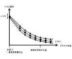
図5は、感光ドラム1が新品状態である場合において、スキャナ3の露光量と、感光ドラム1の表面電位との関係を示した図である。帯電ローラ2に印加される電圧を同様に制御して、複数の感光ドラム1を帯電した場合、図5に示すように、スキャナ3によって露光された後の感光ドラム1の表面電位はばらついてしまう。このようなバラツキは、画像形成装置Aの装置本体100における高圧回路の公差や、感光ドラム1の個体差などによって生じる。図5に示すように、感光ドラム1の暗部電位VD(露光されない部分の電位)には、±60Vのバラツキがある。
<(d) Reference surface potential 1 on photosensitive drum 1>
FIG. 5 is a diagram showing the relationship between the exposure amount of the
図5に示すように、スキャナ3の露光量が大きくなるほど、感光ドラム1の表面電位のバラツキは小さくなることが分かる。そして、本実施例では、記録媒体Pに画像を形成するときよりも大きい露光量(本実施例では3.5mJ/m2)で、感光ドラム1の表面を露光することで基準表面電位1を形成する。このとき、図5に示すように、画像形成装置Aにおける高圧回路の公差や、感光ドラム1の個体差などによる基準表面電位1のバラツキは±10Vとなる。感光ドラム1の表面電位の測定値を補正する方法については、後ほど具体的に説明する。
As shown in FIG. 5, it can be seen that the larger the exposure amount of the
ここで、画像形成時におけるスキャナ3の露光量は、明部電位VLが安定するように決定されるとともに、感光ドラム1に形成される静電潜像のパターンの諧調性を考慮して決定される。一方で、基準表面電位1は、感光ドラム1の表面電位の安定性のみを考慮して決定すればよい。そのため、例えば、画像形成時のスキャナ3の露光量で、感光ドラム1の表面電位のバラツキが小さい場合、画像形成時のスキャナ3の露光量で、感光ドラム1上に基準表面電位1を形成してもよい。なお、本実施例のように、画像形成時におけるスキャナ3の露光量よりも大きい露光量で、感光ドラム1上に基準表面電位1を形成することがより好ましい。
Here, the exposure amount of the
<(3)本実施例における画像形成動作の流れ>
図1は、本実施例における画像形成動作の流れを示すフローチャートである。本実施例では、感光ドラム1に形成された基準表面電位1から、感光ドラム1の表面電位の測定値を補正することで、感光ドラム1の暗部電位VDを所望にしている。以下に、図1を用いて、本実施例における画像形成動作の流れを説明する。
<(3) Flow of image forming operation in this embodiment>
FIG. 1 is a flowchart showing the flow of the image forming operation in this embodiment. In this embodiment, the dark portion potential V D of the photosensitive drum 1 is desired by correcting the measured value of the surface potential of the photosensitive drum 1 from the reference surface potential 1 formed on the photosensitive drum 1. The flow of the image forming operation in this embodiment will be described below with reference to FIG.
S1000:ユーザからプリントジョブ実行の指示が入力され、それに基づき、制御部Sが画像形成装置Aの動作を制御することで、プリントジョブがスタートする。
S1001:制御部Sが、記憶部としてのメモリ50に記憶されたプログラムを実行することで、カートリッジに備えられているメモリ50の情報を取得する。例えば、制御部Sがメモリ50に記憶されたプログラムを実行することで、メモリ50から、感光ドラム1の総回転数を取得する。
S1000: The user inputs an instruction to execute a print job, and the control unit S controls the operation of the image forming apparatus A based on the instruction to start the print job.
S1001: The control unit S acquires the information of the
S1002:制御部Sがメモリ50に記憶されたプログラムを実行することで、カートリッジが新品、または、カートリッジが新品に近い状態であるか否かの情報を取得する。例えば、メモリ50には、カートリッジが新品に近い状態であるかを判断するための閾値が予め記憶されており、閾値以上となる場合に、カートリッジは新品に近い状態であると判断される。例えば、感光ドラム1の総回転数が500回を超えるまでは、カートリッジは新品に近い状態であると判断される。
S1002: The control unit S executes the program stored in the
S1003:制御部Sが帯電電圧印加回路2aの動作を制御することで、帯電電圧印加回路2aは帯電ローラ2に所定の電圧を印加し、これにより、帯電ローラ2が感光ドラム1を帯電する。また、制御部Sがスキャナ3の動作を制御することで、スキャナ3が所定の露光量で感光ドラム1を露光し、感光ドラム1の表面の電位を基準表面電位1とする。ここで、本実施例では、基準表面電位1は、温湿度環境や、帯電ローラ2に印加されるバイアスのずれや、帯電ローラ2の公差によるずれなどに起因する誤差が±10Vとなるような電位である。
S1003: The control unit S controls the operation of the charging
なお、本実施例では、図5に示すように、感光ドラム1に照射される露光量が0である場合、温湿度環境や、帯電ローラ2に印加されるバイアスのずれや、帯電ローラ2の公差によるずれなどに起因する誤差は±60Vとなる。ここで、温湿度環境や、帯電ローラ2に印加されるバイアスのずれや、帯電ローラ2の公差によるずれなどに起因する誤差と、感光ドラム1に照射される露光量との関係は、予め実験によって求められており、予めメモリ50に記憶されていることとする。スキャナ3は、誤差が±10Vとなるような露光量で感光ドラム1を露光する。
In this embodiment, as shown in FIG. 5, when the exposure amount applied to the photosensitive drum 1 is 0, the temperature/humidity environment, the bias deviation applied to the charging roller 2, the charging roller 2 The error caused by the deviation due to the tolerance is ±60V. Here, the relationship between the error due to the temperature and humidity environment, the deviation of the bias applied to the charging roller 2, the deviation due to the tolerance of the charging roller 2, and the exposure amount irradiated on the photosensitive drum 1 was previously tested. It is calculated by the following method and is stored in the
S1004:制御部Sが転写ローラ5の動作を制御することで、転写ローラ5は、感光ドラム1の表面電位を測定する。具体的には、上述したように、図4に示すグラフと式(1)と放電開始電圧V1と放電開始電圧V2とから、感光ドラム1表面(像担持体表面)の電位を測定する。ここで、上記説明では、感光ドラム1の明部電位VLを求めていたが、同様の方法で、感光ドラム1の表面電位も測定することとする。
S1004: The control section S controls the operation of the
S1005:制御部Sがメモリ50に記憶されたプログラムを実行することで、感光ドラム1の表面電位の測定値の誤差であって、転写ローラ5で測定することによる誤差を導出する。具体的には、感光ドラム1の表面電位を基準表面電位1とした状態において、感光ドラム1の表面電位の測定値(転写ローラ5による測定値)と、感光ドラム1の表面電位の目標値との差を、転写ローラ5に起因する測定値の誤差とする。
S1005: The control unit S executes the program stored in the
本実施例において、メモリ50には、予め、感光ドラム1の表面電位を基準表面電位1とした状態における感光ドラム1の表面電位の目標値が記憶されている。また、制御部S
がメモリ50に記憶されたプログラムを実行することで、感光ドラム1の表面電位の測定値と、感光ドラム1の表面電位の目標値との差を導き出す。そして、この感光ドラム1の表面電位の測定値と、感光ドラム1の表面電位の目標値との差を、転写ローラ5に起因する測定値の誤差と見なしている。この誤差を補正量として、感光ドラム1の表面電位の測定値を補正する。
In this embodiment, the target value of the surface potential of the photosensitive drum 1 when the surface potential of the photosensitive drum 1 is set to the reference surface potential 1 is stored in the
By executing the program stored in the
本実施例において、例えば、感光ドラム1に照射される露光量を0にした場合、図5に示すように、帯電ローラ2に印加されるバイアスのずれなどに起因する感光ドラム1の表面電位のバラツキは±60Vとなる。そして、この場合に、感光ドラム1の表面電位の測定値と、感光ドラム1の表面電位の目標値との差を、転写ローラ5に起因する測定値の誤差と見なすと、この誤差のバラツキも±60Vとなってしまう。
In the present embodiment, for example, when the exposure amount applied to the photosensitive drum 1 is set to 0, as shown in FIG. The variation is ±60V. Then, in this case, if the difference between the measured value of the surface potential of the photosensitive drum 1 and the target value of the surface potential of the photosensitive drum 1 is regarded as an error of the measured value caused by the
しかし、本実施例では、誤差の測定は、帯電ローラ2に印加されるバイアスのずれなどに起因する感光ドラム1の表面電位のバラツキが±10Vである状態で行われている。そのため、転写ローラ5に起因する測定値の誤差のバラツキも±10Vとなる。つまり、本実施例では、転写ローラ5に起因する誤差以外の誤差が微小(±10V)となる状態において、感光ドラム1の表面電位の測定値と、感光ドラム1の表面電位の目標値との差を、転写ローラ5に起因する誤差と見なしている。これにより、転写ローラ5に起因する誤差を精度よく求めることができるため、感光ドラム1の表面電位を精度よく測定することができる。
However, in this embodiment, the measurement of the error is performed in the state where the variation of the surface potential of the photosensitive drum 1 due to the deviation of the bias applied to the charging roller 2 is ±10V. Therefore, the variation in the error of the measurement value due to the
S1006:制御部Sがメモリ50に記憶されたプログラムを実行することで、S1005において導出された補正値に基づいて、感光ドラム1の表面電位の測定値を補正する。具体的には、転写ローラ5によって測定された感光ドラム1の表面電位に測定値から、S1005で求めた補正値を加算・減算することで、感光ドラム1の表面電位に測定値を補正する。これにより、精度よく、感光ドラム1の表面電位を測定することができる。
S1006: The control unit S executes the program stored in the
S1007:補正された感光ドラム1の表面電位の測定値に基づいて、帯電ローラ2の感光ドラム1への帯電量を導出し、その帯電量で感光ドラム1が帯電される。具体的には、メモリ50には、関係式(第2関係に対応)(帯電量=初期の帯電量+係数A×感光ドラム1の回転数(初期の帯電量は、例えば、初期の感光ドラム1の表面電位と初期の帯電量との関係が示されたテーブルによって求める。))が記憶されている。そして、この関係式を用いて、感光ドラム1への帯電量を決定する。本実施例では、初期の感光ドラム1の表面電位の測定精度が高いため、初期の帯電量が所望の値となり、感光ドラム1の暗部電位VDを所望の値に近づけることができる。これにより、暗部電位VDに対応する部分にトナーが転写されてしまうこと(カブリ)を抑制することができる。なお、感光ドラム1の表面において、暗部電位VD部以外の部分が露光されることで、感光ドラム1の表面に明部電位VL部が形成される。ここで、本実施例では、帯電ローラ2の帯電量を変化させることで、感光ドラム1の暗部電位VDを所望の値にしている。しかし、必ずしもこれに限られることはなく、例えば、スキャナ3の露光量を変化させることで、感光ドラム1の暗部電位VDを所望の値にしてもよい。
S1007: The charge amount of the charging roller 2 to the photosensitive drum 1 is derived based on the corrected measured surface potential of the photosensitive drum 1, and the photosensitive drum 1 is charged with the charged amount. Specifically, in the
また、本実施例では、上記関係式に示すように、カートリッジの使用状況(感光ドラム1の回転数)に応じて、感光ドラム1への帯電量を補正している。ここで、例えば、カートリッジを長期間使用した場合には、感光ドラム1の膜厚が薄くなるため、露光後の感光ドラム1の表面電位も変化してしまう。しかし、本実施例のように、カートリッジの使用状況に応じて、感光ドラム1への帯電量を変化させることで、感光ドラム1の表面電位を所望の値にすることができる。 Further, in the present embodiment, as shown in the above relational expression, the charge amount on the photosensitive drum 1 is corrected according to the usage status of the cartridge (rotational speed of the photosensitive drum 1). Here, for example, when the cartridge is used for a long period of time, the film thickness of the photosensitive drum 1 becomes thin, so that the surface potential of the photosensitive drum 1 after exposure also changes. However, as in this embodiment, the surface potential of the photosensitive drum 1 can be set to a desired value by changing the amount of charge on the photosensitive drum 1 according to the usage status of the cartridge.
S1008:制御部Sが、画像形成装置A内の機器の動作を制御することで、画像形成
装置Aはプリント動作を実行する。具体的には、制御部Sが、現像装置や転写ローラ5や定着装置6などの動作を制御することで、記録媒体Pに画像が形成される。
S1009:プリント動作の終了後、S1007で求められた初期の帯電量と、S1001で取得された情報(例えば、感光ドラム1の回転数)などはメモリ50に記憶される。
S1010:画像形成装置A内の機器の動作を制御部Sが制御することで、プリントジョブが終了する。
S1008: The control unit S controls the operation of the devices in the image forming apparatus A, so that the image forming apparatus A executes the print operation. Specifically, the control unit S controls the operations of the developing device, the
S1009: After the printing operation is completed, the initial charge amount obtained in S1007, the information obtained in S1001 (for example, the rotation speed of the photosensitive drum 1) and the like are stored in the
S1010: The control unit S controls the operation of the device in the image forming apparatus A, and the print job is completed.
S1011:メモリ50に記憶されている初期の帯電量(S1007で求められた値)と、感光ドラム1の回転数と、S1007で用いた式とに基づいて、感光ドラム1への帯電量を導出する。そして、その帯電量で感光ドラム1が帯電される。これにより、上述したように、カブリの発生を抑制する。また、同時に、感光ドラム1が露光されることで、感光ドラム1の表面に明部電位VL部が形成される。
S1011: The charge amount to the photosensitive drum 1 is derived based on the initial charge amount (the value obtained in S1007) stored in the
S1012:制御部Sが、画像形成装置A内の機器の動作を制御することで、上述したように、画像形成装置はプリント動作を実行する。
S1013:プリント動作の終了後、S1001で取得された情報(例えば、感光ドラム1の回転数)がメモリ50に保存される。
S1014:画像形成装置A内の機器の動作を制御部Sが制御することで、プリントジョブが終了する。
S1012: The control unit S controls the operation of the devices in the image forming apparatus A, and as described above, the image forming apparatus executes the print operation.
S1013: After the printing operation is completed, the information (for example, the number of rotations of the photosensitive drum 1) acquired in S1001 is stored in the
S1014: The control unit S controls the operation of the device in the image forming apparatus A, and the print job is completed.
なお、本実施例では、S1009およびS1013において、感光ドラム1の使用状況(感光ドラム1の総回転数など)はメモリ50に記憶されたが、必ずしもこれに限られない。感光ドラム1における暗部電位VDと現像スリーブ4の電位との差を所望の値にすることができればよい。例えば、S1005において得られた補正量がメモリ50に保存され、S1011において、この補正量を用いて、感光ドラム1における暗部電位VD部を形成してもよい。
In this embodiment, the usage status of the photosensitive drum 1 (such as the total number of rotations of the photosensitive drum 1) is stored in the
また、本実施例では、カートリッジが寿命に到達するまで適正な画像が形成されるように暗部電位VDを所望の値にしたが、必ずしもこれに限られない。暗部電位VDと現像スリーブ4の電位との差(以下、電位差Vbackとする)を所望の値にすることができればよく、例えば、現像スリーブ4の電位を補正することで、電位差Vbackを所望の値にしてもよい。
Further, in this embodiment, the dark portion potential V D is set to a desired value so that an appropriate image is formed until the life of the cartridge is reached, but the present invention is not limited to this. It suffices that the difference between the dark portion potential V D and the potential of the developing sleeve 4 (hereinafter referred to as the potential difference V back ) be set to a desired value. For example, by correcting the potential of the developing
<(4)比較例1について>
実施例1の効果を説明するために比較例1について説明する。図8は、比較例1における画像形成動作の流れを示すフローチャートである。比較例1では、実施例1とは異なり、感光ドラム1の表面電位を測定する際に測定値を補正しない。
S1100:実施例1におけるS1000と同様に、プリントジョブがスタートする。
S1101:実施例1におけるS1001と同様に、制御部Sがメモリ50に記憶されるプログラムを実行することで、カートリッジの使用状況が取得される。
<(4) About Comparative Example 1>
Comparative Example 1 will be described in order to explain the effect of Example 1. FIG. 8 is a flowchart showing the flow of the image forming operation in Comparative Example 1. Unlike Comparative Example 1, Comparative Example 1 does not correct the measured value when measuring the surface potential of the photosensitive drum 1.
S1100: A print job is started as in S1000 in the first embodiment.
S1101: Similar to S1001 in the first embodiment, the control unit S executes the program stored in the
S1102:メモリ50に保存されている情報に基づいて、暗部電位VD部を形成するための露光量を導出する。具体的には、メモリ50には、関係式(露光量=初期の露光量+係数A×感光ドラム1の回転数)が記憶されている。しかし、比較例1では、実施例1とは異なり、初期の感光ドラム1の表面電位の測定値が補正されないため、初期の露光量が所望の値にならない。そのため、比較例1では、暗部電位VDが所望の値にならず、記録媒体Pにカブリが発生してしまうおそれがある。
S1103:実施例1におけるS1008と同様に、プリント動作を開始する。
S1104:実施例1におけるS1009と同様に、プリント動作の終了後に、感光ド
ラム1の使用状況がメモリ50に保存される。
S1105:実施例1におけるS1010と同様に、プリントジョブが終了する。
S1102: The exposure amount for forming the dark portion potential V D portion is derived based on the information stored in the
S1103: Similar to S1008 in the first embodiment, the print operation is started.
S1104: Similar to S1009 in the first embodiment, the usage status of the photosensitive drum 1 is stored in the
S1105: As with S1010 in the first embodiment, the print job ends.
<(4)比較例1に対する実施例1の優位な点>
実施例1において、カートリッジが長期間使用された後における暗部電位VDの値について考える。本実施例における感光ドラム1の表面電位の測定値の誤差は、上述したように±10Vだけばらつく。そして、カートリッジが長期間使用された後において、感光ドラム1の膜厚が薄くなることで、感光ドラム1の表面電位の測定値の誤差がさらに±10Vばらつくとする。この場合、感光ドラム1の暗部電位VDの値は、合計して±20Vだけばらつくこととなる。
<(4) Advantages of Example 1 over Comparative Example 1>
In Example 1, the value of the dark portion potential V D after the cartridge has been used for a long time will be considered. The error in the measured value of the surface potential of the photosensitive drum 1 in this embodiment varies by ±10 V as described above. Then, after the cartridge has been used for a long period of time, the film thickness of the photosensitive drum 1 becomes thin, and the error in the measured value of the surface potential of the photosensitive drum 1 further varies by ±10V. In this case, the value of the dark portion potential V D of the photosensitive drum 1 varies by ±20 V in total.
次に、比較例1において、カートリッジが長期間使用された後における暗部電位VDの値について考える。比較例1では、本実施例とは異なり、感光ドラム1の表面電位の測定値の誤差は±60Vの範囲でばらつく。そして、カートリッジが長期間使用された後において、感光ドラム1の膜厚が薄くなることで、感光ドラム1の表面電位の測定値の誤差がさらに±10Vばらつくとする。この場合、感光ドラム1の暗部電位VDの値は、合計して±70Vだけばらつくこととなる。 Next, in Comparative Example 1, the value of the dark portion potential V D after the cartridge has been used for a long time will be considered. In Comparative Example 1, unlike the present Example, the error in the measured value of the surface potential of the photosensitive drum 1 varies within the range of ±60V. Then, after the cartridge has been used for a long period of time, the film thickness of the photosensitive drum 1 becomes thin, and the error in the measured value of the surface potential of the photosensitive drum 1 further varies by ±10V. In this case, the value of the dark portion potential V D of the photosensitive drum 1 varies by ±70 V in total.
ここで、図9は、カートリッジが長期間使用された後における電位差Vback(暗部電位VDと現像スリーブ4の電位との差)と、記録媒体Pに生じたカブリの濃度との関係を示す図である。カブリの濃度と電位差Vbackとの関係性は、図9に示したような関係性となる。ここで、適正な画像を得るためには、カブリの濃度が許容値以下である必要がある。カブリの濃度が許容値よりも大きいと、ユーザがカブリを視認することができてしまう。 Here, FIG. 9 shows the relationship between the potential difference V back (difference between the dark portion potential V D and the potential of the developing sleeve 4) after the cartridge has been used for a long time, and the density of the fog on the recording medium P. It is a figure. The relationship between the fog density and the potential difference V back is as shown in FIG. Here, in order to obtain a proper image, the fog density needs to be equal to or less than the allowable value. If the fog density is higher than the allowable value, the user can visually recognize the fog.
また、図9には、カブリ濃度の許容値と、実施例1と比較例1とにおける電位差Vback(暗部電位VDと現像スリーブ4の電位との差)のバラツキの範囲も示している。図9に示すように、比較例1では、カートリッジが長期間使用された後において、カブリ濃度が許容値を超えてしまい、適正な画像を得ることができない可能性がある。これに対して、実施例1では、カブリ濃度が許容値を超えることがなく、適正な画像を得ることができる。このように、カブリの濃度において、実施例1は、比較例1よりも優れていることが分かる。 FIG. 9 also shows the permissible value of the fog density and the range of variations in the potential difference V back (difference between the dark portion potential V D and the potential of the developing sleeve 4) between Example 1 and Comparative Example 1. As shown in FIG. 9, in Comparative Example 1, the fog density exceeds the permissible value after the cartridge has been used for a long period of time, and it may not be possible to obtain an appropriate image. On the other hand, in Example 1, the fog density does not exceed the allowable value, and an appropriate image can be obtained. Thus, it can be seen that Example 1 is superior to Comparative Example 1 in the fog density.
以上のように、本実施例では、帯電された感光ドラム1が、転写ローラ5に起因しない測定値の誤差が微差となる露光量で露光される。また、感光ドラム1が露光された後の表面電位の目標値と測定値との差を、転写ローラ5に起因する誤差として、転写ローラ5に起因する誤差に基づいて、感光ドラム1の表面電位の測定値を補正する。そして、補正された測定値に基づいて、感光ドラム1の表面電位が目標値となるように、帯電ローラ2に印加される電圧と、スキャナ3の露光量の少なくともいずれか1つを制御する。これにより、感光ドラム1における暗部電位VDを適正な値にすることができる。
As described above, in the present embodiment, the charged photosensitive drum 1 is exposed with the exposure amount such that the error of the measurement value not caused by the
(実施例2)
次に、実施例2について説明する。実施例2では、実施例1と異なり、カートリッジの使用を開始したときから、カートリッジが寿命に達するまで、感光ドラム1における暗部電位VDと明部電位VLとを所望の値にすることができる。ここで、実施例2において、実施例1と同一の機能を有する部分については、同一の符号を付すことでその説明を省略する。
(Example 2)
Next, a second embodiment will be described. In the second embodiment, unlike the first embodiment, the dark portion potential V D and the light portion potential VL of the photosensitive drum 1 can be set to desired values from the start of use of the cartridge until the life of the cartridge is reached. it can. Here, in the second embodiment, the portions having the same functions as those of the first embodiment are designated by the same reference numerals and the description thereof will be omitted.
<(1)本実施例の構成について>
本実施例の構成について詳細に説明する。
<(a)基準表面電位>
本実施例では、実施例1と同様に、感光ドラム1の使用開始時(カートリッジが新品状態であるとき)に、基準表面電位1に基づいて、感光ドラム1の表面電位の値を補正する。これに加えて、本実施例では、感光ドラム1における明部電位VLも安定させることができる。
<(1) Constitution of this embodiment>
The configuration of this embodiment will be described in detail.
<(a) Reference surface potential>
In the present embodiment, as in the first embodiment, the value of the surface potential of the photosensitive drum 1 is corrected based on the reference surface potential 1 at the start of use of the photosensitive drum 1 (when the cartridge is in a new state). In addition to this, in the present embodiment, the bright portion potential VL on the photosensitive drum 1 can also be stabilized.
図6は、感光ドラム1の寿命後半(カートリッジが長期間使用された後)におけるスキャナ3の露光量と感光ドラム1の明部電位VLとの関係を示す図である。図6に示すように、実施例1にように暗部電位VDの値を補正したとしても、感光ドラム1の寿命後半において、感光ドラム1の明部電位VLにバラツキが生じてしまう場合がある。なお、図6における感光ドラム1の明部電位VLの誤差±50Vは、感光ドラム1の抵抗値の変動や、感光ドラム1の感光層の感度の変動や、感光層の膜厚のムラや、使用環境(温度や湿度など)によって生じる。
FIG. 6 is a diagram showing the relationship between the exposure amount of the
ここで、上述したように、本実施例では、感光ドラム1の寿命後半において、感光ドラム1における明部電位VLのバラツキは±50Vとなっている。これは、感光ドラム1が使用されるにつれて、感光ドラム1の感光層の削れや、感光ドラム1における感光層の感度の悪化などが大きく変化するためである。そのため、本実施例では、感光ドラム1の寿命後半において、感光ドラム1の表面に基準表面電位2を形成する。本実施例では、基準表面電位2を形成するための感光ドラム1への露光量(第2露光量)は0となっている。ここで、感光ドラム1の表面電位が基準表面電位2となっているとき、感光ドラム1の表面電位のバラツキは±10Vである。 Here, as described above, in this embodiment, in the latter half of the life of the photosensitive drum 1, the variation of the bright portion potential V L on the photosensitive drum 1 is ±50V. This is because as the photosensitive drum 1 is used, the abrasion of the photosensitive layer of the photosensitive drum 1 and the deterioration of the sensitivity of the photosensitive layer of the photosensitive drum 1 change greatly. Therefore, in this embodiment, the reference surface potential 2 is formed on the surface of the photosensitive drum 1 in the latter half of the life of the photosensitive drum 1. In this embodiment, the exposure amount (second exposure amount) on the photosensitive drum 1 for forming the reference surface potential 2 is zero. Here, when the surface potential of the photosensitive drum 1 is the reference surface potential 2, the variation of the surface potential of the photosensitive drum 1 is ±10V.
<(2)本実施例における画像形成動作の流れ>
図7は、本実施例における画像形成動作の流れを示すフローチャートである。本実施例では、感光ドラム1の表面電位を基準表面電位2にすることで、感光ドラム1の表面電位の測定値を補正する。これにより、感光ドラム1において、明部電位VLと暗部電位VDとを所望の値にすることができる。
<(2) Flow of image forming operation in this embodiment>
FIG. 7 is a flowchart showing the flow of the image forming operation in this embodiment. In this embodiment, the measured surface potential of the photosensitive drum 1 is corrected by setting the surface potential of the photosensitive drum 1 to the reference surface potential 2. As a result, in the photosensitive drum 1, the light portion potential V L and the dark portion potential V D can be set to desired values.
S2000:実施例1におけるS1000と同様に、プリントジョブがスタートする。
S2001:実施例1におけるS1001と同様に、制御部Sがメモリ50に記憶されるプログラムを実行することで、カートリッジの使用状況が取得される。
S2002:実施例1におけるS1002と同様に、制御部Sがメモリ50に記憶されたプログラムを実行することで、カートリッジが新品、または、カートリッジが新品に近い状態であるか否かの情報を取得する。カートリッジが新品状態であると判断された場合S2003に進み、カートリッジが新品状態でないと判断された場合S2011に進む。
S2000: A print job is started in the same manner as S1000 in the first embodiment.
S2001: Similar to S1001 in the first embodiment, the control unit S executes the program stored in the
S2002: Similar to S1002 in the first embodiment, the control unit S executes the program stored in the
S2003:実施例1におけるS1003と同様に、帯電ローラ2に所定のバイアスが印加され、感光ドラム1が帯電される。また、スキャナ3が所定の露光量で感光ドラム1を露光し、感光ドラム1の表面の電位を基準表面電位1とする。
S2004:実施例1におけるS1004と同様に、転写ローラ5は、感光ドラム1の表面電位を測定する。
S2003: Similar to S1003 in Embodiment 1, a predetermined bias is applied to the charging roller 2 to charge the photosensitive drum 1. Further, the
S2004: Similar to S1004 in the first embodiment, the
S2005:実施例1におけるS1005と同様に、感光ドラム1の表面電位の測定値の誤差であって、転写ローラ5で測定することによる誤差を導出する。具体的には、感光ドラム1の表面電位を基準表面電位1とした状態において、感光ドラム1の表面電位の測定値(転写ローラ5による測定値)と、感光ドラム1の表面電位の目標値との差を、転写ローラ5に起因する測定値の誤差とする。そして、この誤差を補正量1とする。
S2005: Similar to S1005 in the first embodiment, the error in the measured value of the surface potential of the photosensitive drum 1 which is due to the measurement by the
S2006:実施例1におけるS1006と同様に、S2005において導出された補
正量1に基づいて、感光ドラム1の明部電位VLと暗部電位VDの測定値を補正する。具体的には、まず、転写ローラ5によって、感光ドラム1における明部電位VLと暗部電位VDとが測定される。そして、転写ローラ5によって測定された感光ドラム1の表面電位に測定値から、S2005で求めた補正値を加算・減算することで、明部電位VLと暗部電位VDの測定値を補正する。これにより、精度よく、感光ドラム1の表面電位を測定することができる。また、その補正された明部電位VLおよび暗部電位VDの測定値と、帯電ローラ2に印加されるバイアスと、スキャナ3の露光量との関係が導き出される。そして、この明部電位VLおよび暗部電位VDの測定値と、帯電ローラ2に印加されるバイアスと、スキャナ3の露光量との関係はメモリ50に保存される。なお、本実施例では、暗部電位は、帯電ローラ2に印加されるバイアスのみによって決定される。
S2006: Similar to S1006 in the first embodiment, the measured values of the light portion potential V L and the dark portion potential V D of the photosensitive drum 1 are corrected based on the correction amount 1 derived in S2005. Specifically, first, the
S2007:S2006においてメモリ50に記憶された情報(明部電位VLおよび暗部電位VDの測定値と、帯電ローラ2に印加されるバイアスと、スキャナ3の露光量との関係)に基づいて、明部電位VLおよび暗部電位VDを所定の電位にする。具体的には、S2006においてメモリ50に記憶された情報に基づいて、明部電位VLおよび暗部電位VDが目標値となるように、帯電ローラ2に印加されるバイアスと、スキャナ3の露光量とが制御される。これにより、明部電位VLおよび暗部電位VDの値が所望の値となる。
S2007: Based on the information stored in the
ここで、本実施例では、実施例1とは異なり、感光ドラム1における明部電位VL部への帯電量および露光量についても補正される。本実施例では、初期の感光ドラム1の表面電位の測定精度が高いため、初期の露光量が所望の値となり、感光ドラム1の明部電位VLおよび暗部電位VDを所望の値に近づけることができる。これにより、明部電位VLに対応する部分にトナーが転写されないことを抑制するとともに、暗部電位VDに対応する部分にトナーが転写されてしまうこと(カブリ)を抑制することができる。 Here, in the present embodiment, unlike the first embodiment, the charge amount and the exposure amount to the bright portion potential V L portion of the photosensitive drum 1 are also corrected. In this embodiment, since the measurement accuracy of the surface potential of the initial photosensitive drum 1 is higher, the initial exposure is a desired value, approximate the bright potential V L and the dark potential V D of the photosensitive drum 1 to a desired value be able to. As a result, it is possible to prevent the toner from being transferred to the portion corresponding to the light portion potential V L and to prevent the toner from being transferred (fogging) to the portion corresponding to the dark portion potential V D.
S2008:実施例1におけるS1008と同様に、画像形成装置Aはプリント動作を実行する。具体的には、制御部Sが、現像装置や転写ローラ5や定着装置6などの動作を制御することで、記録媒体Pに画像が形成される。
S2009:プリント動作の終了後、S2006で求められた情報(明部電位VLおよび暗部電位VDの測定値と、帯電ローラ2に印加されるバイアスと、スキャナ3の露光量との関係)がメモリ50に記憶される。また、プリント動作の終了後、S2001で取得された情報(例えば、感光ドラム1の回転数)などがメモリ50に記憶される。
S2010:画像形成装置A内の機器の動作を制御部Sが制御することで、プリントジョブが終了する。
S2008: Similar to S1008 in the first embodiment, the image forming apparatus A executes the print operation. Specifically, the control unit S controls the operations of the developing device, the
S2009: After the printing operation is completed, the information (relationship between the measured value of the light portion potential V L and the dark portion potential V D , the bias applied to the charging roller 2 and the exposure amount of the scanner 3) obtained in S2006 is obtained. It is stored in the
S2010: The control unit S controls the operation of the device in the image forming apparatus A, and the print job is completed.
S2011:メモリ50に保存されている情報(S2006で取得された対応関係や、感光ドラム1の使用状況など)に基づいて、感光ドラム1における基準表面電位2を導出する。上述したように、本実施例では、メモリ50には、明部電位VLおよび暗部電位VDを求めるための対応関係(明部電位VLおよび暗部電位VDの測定値と、帯電ローラ2に印加されるバイアスと、スキャナ3の露光量との関係)が記憶されている。また、メモリ50には、この対応関係や、感光ドラム1の走行距離(感光ドラム1の外周面の総移動距離)などと、基準表面電位2との対応関係が保存されている。そして、本実施例では、メモリ50に記憶されているこれらの情報と、感光ドラム1の走行距離などとによって、感光ドラム1における基準表面電位2が導き出される。なお、本実施例において、明部電位VLおよび暗部電位VDを求めるための対応関係は、例えばテーブルである。
S2011: The reference surface potential 2 of the photosensitive drum 1 is derived based on the information stored in the memory 50 (corresponding relationship acquired in S2006, usage status of the photosensitive drum 1, etc.). As described above, in this embodiment, the
S2012:実施例1におけるS1003と同様に、帯電ローラ2に所定のバイアスが印加され、感光ドラム1が帯電される。ここで、本実施例では、スキャナ3が感光ドラム1を露光することなく(露光量0)、感光ドラム1の表面の電位が基準表面電位2になる
。具体的には、メモリ50には、感光ドラム1の表面電位と、帯電ローラ2に印加されるバイアスと、スキャナ3の露光量との対応関係が記憶されている。そして、この対応関係に基づいて、帯電ローラ2に印加されるバイアスと、スキャナ3の露光量とが決定される。
S2013:実施例1におけるS1004と同様に、転写ローラ5は、感光ドラム1の表面電位を測定する。
S2012: Similar to S1003 in the first embodiment, a predetermined bias is applied to the charging roller 2 to charge the photosensitive drum 1. Here, in this embodiment, the potential of the surface of the photosensitive drum 1 becomes the reference surface potential 2 without the
S2013: Similar to S1004 in Embodiment 1, the
S2014:実施例1におけるS1005と同様に、感光ドラム1の明部電位VLの測定値の誤差であって、転写ローラ5で測定することによる誤差を導出する。具体的には、感光ドラム1の表面電位を基準表面電位2とした状態において、感光ドラム1の表面電位の測定値(転写ローラ5による測定値)と、感光ドラム1の表面電位の目標値との差を、転写ローラ5に起因する測定値の誤差とする。そして、この誤差を補正量2とする。
S2014: Similar to S1005 in the first embodiment, the error of the measured value of the light portion potential VL of the photosensitive drum 1 which is due to the measurement by the
S2015:転写ローラ5によって、感光ドラム1における明部電位VLが測定される。そして、転写ローラ5によって測定された明部電位VLは補正量2によって補正される。これにより、感光ドラム1における明部電位VLの測定値は適切な値に補正される。
S2016:S2015における測定結果と、メモリ50に保存されている情報(S2006で取得された対応関係や、感光ドラム1の使用状況など)に基づいて、感光ドラム1における明部電位VLを所望の値にする。具体的には、実施例1におけるS1007と同様に、補正された感光ドラム1の明部電位VLの測定値に基づいて、帯電ローラ2の感光ドラム1への帯電量と、スキャナ3の感光ドラム1への露光量とを導出する。そして、導き出された露光量と帯電量で、感光ドラム1が帯電・露光される。これにより、感光ドラム1における明部電位VLが所望の値となる。
S2015: The
S2016: Based on the measurement result in S2015 and the information stored in the memory 50 (correspondence obtained in S2006, usage status of the photosensitive drum 1, etc.), the bright portion potential V L of the photosensitive drum 1 is desired. Value. Specifically, similar to S1007 in the first embodiment, the charge amount of the charging roller 2 onto the photosensitive drum 1 and the exposure of the
一方、感光ドラム1における暗部電位VDは、実施例1におけるS1007と同様の方法で所望の値となる。具体的には、補正量1によって補正された感光ドラム1の表面電位の測定値に基づいて、帯電ローラ2の感光ドラム1への帯電量を導出し、その帯電量で感光ドラム1が帯電される。 On the other hand, the dark portion potential V D on the photosensitive drum 1 becomes a desired value by the same method as S1007 in the first embodiment. Specifically, the charge amount of the charging roller 2 to the photosensitive drum 1 is derived based on the measured surface potential of the photosensitive drum 1 corrected by the correction amount 1, and the photosensitive drum 1 is charged with the charged amount. It
S2017:実施例1におけるS1008と同様に、画像形成装置Aはプリント動作を実行する。
S2018:実施例1におけるS1009と同様に、プリント動作の終了後、S2007で求められた初期の露光量と、S2001で取得された情報(例えば、感光ドラム1の回転数)などがメモリ50に記憶される。
S2019:画像形成装置A内の機器の動作を制御部Sが制御することで、プリントジョブが終了する。
S2017: Similar to S1008 in the first embodiment, the image forming apparatus A executes the print operation.
S2018: Similar to S1009 in the first embodiment, after the printing operation is completed, the initial exposure amount obtained in S2007, the information obtained in S2001 (for example, the rotation speed of the photosensitive drum 1) and the like are stored in the
S2019: The control unit S controls the operation of the device in the image forming apparatus A, and the print job ends.
なお、本実施例では、S2009およびS2018において、感光ドラム1の使用状況(感光ドラム1の総回転数など)はメモリ50に記憶されたが、必ずしもこれに限られない。感光ドラム1における暗部電位VDと現像スリーブ4の電位との差を所望の値にすることができればよい。例えば、S2005において得られた補正量がメモリ50に保存され、S1011において、この補正量1を用いて、感光ドラム1における暗部電位VD部を形成してもよい。
In this embodiment, the usage status of the photosensitive drum 1 (such as the total number of rotations of the photosensitive drum 1) is stored in the
また、本実施例では、カートリッジが寿命に到達するまで適正な画像が形成されるように暗部電位VDを所望の値にしたが、必ずしもこれに限られない。暗部電位VDと現像スリーブ4の電位との差(以下、電位差Vbackとする)と、明部電位VLと現像スリーブ4の電位との差(以下、電位差Vcontとする)を所望の値にすることができればよい。例えば、現像スリーブ4の電位を補正することで、電位差Vcontと電位差Vbackを所望の値にしてもよい。
Further, in this embodiment, the dark portion potential V D is set to a desired value so that an appropriate image is formed until the life of the cartridge is reached, but the present invention is not limited to this. The difference between the dark portion potential V D and the potential of the developing sleeve 4 (hereinafter referred to as the potential difference V back ) and the difference between the light portion potential V L and the potential of the developing sleeve 4 (hereinafter referred to as the potential difference V cont ) are desired. It should be a value. For example, the potential difference V cont and the potential difference V back may be set to desired values by correcting the potential of the developing
<(4)比較例2について>
実施例2の効果を説明するために、比較例1について説明する。比較例2では、実施例2とは異なり、カートリッジの使用開始時に、感光ドラム1の表面電位を基準表面電位1にせず、暗部電位VDについても補正しない。所定のタイミングにおける暗部電位VDを基準電位とし、感光ドラム1の表面電位を補正する。ここで、図10は、比較例2における画像形成動作の流れを示すフローチャートである。
<(4) Comparative Example 2>
In order to explain the effect of Example 2, Comparative Example 1 will be described. In Comparative Example 2, unlike Example 2, the surface potential of the photosensitive drum 1 is not set to the reference surface potential 1 at the start of use of the cartridge, and the dark portion potential V D is not corrected. The surface potential of the photosensitive drum 1 is corrected using the dark portion potential V D at a predetermined timing as a reference potential. Here, FIG. 10 is a flowchart showing the flow of the image forming operation in Comparative Example 2.
S2100:実施例1におけるS1000と同様に、プリントジョブがスタートする。
S2101:実施例1におけるS1001と同様に、制御部Sがメモリ50に記憶されるプログラムを実行することで、カートリッジの使用状況が取得される。
S2102:メモリ50に保存されている情報に基づいて、感光ドラム1の基準電位を導出する。ここで、比較例2では、実施例2とは異なり、基準電位は、転写ローラ5に起因する誤差以外の誤差が微小になるような電位ではない。
S2100: A print job is started in the same manner as S1000 in the first embodiment.
S2101: Similar to S1001 in the first embodiment, the control unit S executes the program stored in the
S2102: The reference potential of the photosensitive drum 1 is derived based on the information stored in the
S2103:制御部Sが帯電ローラ2に印加されるバイアスを制御することで、帯電ローラ2が感光ドラム1を帯電し、感光ドラム1の表面の電位が、S2102で算出された基準電位となる。具体的には、メモリ50には、予め、帯電ローラ2に印加されるバイアスと、感光ドラム1の表面電位との対応関係が記憶されている。そして、メモリ50に記憶された対応関係と、S2102で算出された基準電位とに基づいて、帯電ローラ2印加されるバイアスが決定される。
S2104:実施例1におけるS1004と同様に、転写ローラ5は、感光ドラム1の表面電位を測定する。
S2103: The control unit S controls the bias applied to the charging roller 2, so that the charging roller 2 charges the photosensitive drum 1, and the surface potential of the photosensitive drum 1 becomes the reference potential calculated in S2102. Specifically, the
S2104: Similar to S1004 in the first embodiment, the
S2105:制御部Sがメモリ50に記憶されたプログラムを実行することで、感光ドラム1の表面電位の測定値の誤差であって、転写ローラ5で測定することによる誤差を導出する。具体的には、比較例2では、実施例2とは異なり、基準電位は、転写ローラ5に起因する誤差以外の誤差が微小になるような電位ではない。そのため、転写ローラ5に起因する誤差のバラツキが大きくなり、感光ドラム1の表面電位の補正後の測定値にもバラツキが生じてしまう。
S2105: The control unit S executes the program stored in the
S2106:感光ドラム1を帯電・露光し、転写ローラ5によって、感光ドラム1における明部電位VLを測定する。そして、S2105で導出された補正量を用いて、感光ドラム1における明部電位VLの測定値を補正する。しかし、比較例2では、S2105で導出された補正量が誤差を有しているため、明部電位VLの測定値が適切な値とはならない。
S2106: The photosensitive drum 1 is charged and exposed, and the
S2107:S2106における明部電位VLの測定値および補正量と、メモリ50に保存されているカートリッジの使用状況とに基づいて、感光ドラム1における暗部電位VDと明部電位VLとを所定の値にする。ここで、比較例2では、明部電位VLの測定値と、S2105で求められた補正量とに誤差が生じているため、実際の暗部電位VDと明部電位VLも正しい値とはならない。そのため、比較例2では、カブリなどの画像不良が発生するおそれがある。
S2107: Based on the measured value and the correction amount of the bright portion potential V L in S2106 and the usage status of the cartridge stored in the
S2108:実施例1におけるS1008と同様に、画像形成装置Aはプリント動作を実行する。
S2109:S2101で取得された情報(例えば、感光ドラム1の回転数)などがメモリ50に記憶される。
S2110:画像形成装置A内の機器の動作を制御部Sが制御することで、プリントジョブが終了する。
S2108: The image forming apparatus A executes the printing operation, similarly to S1008 in the first embodiment.
S2109: Information (for example, the number of rotations of the photosensitive drum 1) acquired in S2101 is stored in the
S2110: The control unit S controls the operation of the device in the image forming apparatus A, and the print job is completed.
<(4)比較例2に対する実施例2の優位な点>
実施例2において、カートリッジが長期間使用された後における暗部電位VDの値について考える。本実施例における感光ドラム1の表面電位の測定値の誤差は、上述したように±10Vだけばらつく。そして、カートリッジが長期間使用された後において、感光ドラム1の膜厚が薄くなることで、感光ドラム1の表面電位の測定値の誤差がさらに±10Vばらつくとする。この場合、感光ドラム1の暗部電位VDの値は、合計して±20Vだけばらつくこととなる。一方、感光ドラム1の明部電位VLの値も、同様に、合計して±20Vだけばらつくこととなる。
<(4) Advantages of Example 2 over Comparative Example 2>
In Example 2, the value of the dark portion potential V D after the cartridge has been used for a long time will be considered. The error in the measured value of the surface potential of the photosensitive drum 1 in this embodiment varies by ±10 V as described above. Then, after the cartridge has been used for a long period of time, the film thickness of the photosensitive drum 1 becomes thin, and the error in the measured value of the surface potential of the photosensitive drum 1 further varies by ±10V. In this case, the value of the dark portion potential V D of the photosensitive drum 1 varies by ±20 V in total. On the other hand, similarly, the value of the light portion potential V L of the photosensitive drum 1 also varies by ±20 V in total.
次に、比較例2において、カートリッジが長期間使用された後における暗部電位VDの値について考える。比較例2では、本実施例とは異なり、感光ドラム1の表面電位の測定値の誤差は±60Vの範囲でばらつく。そして、カートリッジが長期間使用された後において、感光ドラム1の膜厚が薄くなることで、感光ドラム1の表面電位の測定値の誤差がさらに±10Vばらつくとする。この場合、感光ドラム1の暗部電位VDの値は、合計して±70Vだけばらつくこととなる。一方、感光ドラム1の明部電位VLの値も、同様に、合計して±70Vだけばらつくこととなる。 Next, in Comparative Example 2, the value of the dark portion potential V D after the cartridge has been used for a long time will be considered. In Comparative Example 2, unlike the present Example, the error in the measured value of the surface potential of the photosensitive drum 1 varies within the range of ±60V. Then, after the cartridge has been used for a long period of time, the film thickness of the photosensitive drum 1 becomes thin, and the error in the measured value of the surface potential of the photosensitive drum 1 further varies by ±10V. In this case, the value of the dark portion potential V D of the photosensitive drum 1 varies by ±70 V in total. On the other hand, similarly, the value of the light portion potential V L of the photosensitive drum 1 also varies by ±70 V in total.
ここで、図11は、カートリッジが長期間使用された後における電位差Vcont(明部電位VLと現像スリーブ4の電位との差)と、記録媒体Pに形成される画像の濃度との関係を示す図である。画像の濃度と電位差Vcontとの関係性は、図11に示したような関係性となる。ここで、適正な画像を得るためには、記録媒体Pに形成される画像の濃度が許容値以上である必要がある。画像の濃度が許容値よりも小さいと、その部分が画像から欠けた状態となってしまう。 Here, FIG. 11 shows the relationship between the potential difference V cont (the difference between the light portion potential V L and the potential of the developing sleeve 4) after the cartridge has been used for a long time, and the density of the image formed on the recording medium P. FIG. The relationship between the image density and the potential difference V cont is as shown in FIG. Here, in order to obtain an appropriate image, the density of the image formed on the recording medium P needs to be equal to or more than the allowable value. If the density of the image is smaller than the allowable value, that portion will be missing from the image.
また、図11には、画像濃度の許容値と、実施例2と比較例2とにおける電位差Vcont(明部電位VLと現像スリーブ4の電位との差)のバラツキの範囲も示している。図11に示すように、比較例2では、カートリッジが長期間使用された後において、画像濃度が許容値を下回ってしまい、適正な画像を得ることができない可能性がある。これに対して、実施例2では、画像濃度が許容値を下回ることがなく、適正な画像を得ることができる。このように、画像の濃度において、実施例2は、比較例2よりも優れていることが分かる。 FIG. 11 also shows the allowable range of the image density and the range of variations in the potential difference V cont (difference between the light portion potential V L and the potential of the developing sleeve 4) between Example 2 and Comparative Example 2. .. As shown in FIG. 11, in Comparative Example 2, after the cartridge has been used for a long period of time, the image density may be below the allowable value, and it may not be possible to obtain an appropriate image. On the other hand, in the second embodiment, it is possible to obtain a proper image without the image density falling below the allowable value. Thus, it can be seen that Example 2 is superior to Comparative Example 2 in image density.
以上のように、本実施例では、カートリッジの劣化度が閾値以下の場合には、感光ドラム1が第1露光量で露光された後における感光ドラム1の表面電位の目標値と測定値との差を、転写ローラ5に起因する第1誤差とする。その第1誤差に基づいて測定値を補正する。そして、補正された測定値に基づいて、感光ドラム1における画像形成部と非画像形成部の電位が目標値となるように、帯電ローラ2に印加される電圧と、スキャナ3の露光量の少なくともいずれか1つを制御する。一方、カートリッジの劣化度が閾値よりも大きい場合には、感光ドラム1が第2露光量で露光された後における感光ドラム1の表面電位の目標値と測定値との差を、転写ローラ5に起因する第2誤差とする。その第2誤差に基づいて測定値を補正する。そして、メモリ50に記憶された第1誤差を用いて補正された測定値に基づいて、非画像形成部の電位が目標値となるように、帯電ローラ2に印加される電圧と、スキャナ3の露光量の少なくともいずれか1つを制御する。また、第2誤差を用いて補正された測定値に基づいて、画像形成部の電位が目標値となるように、帯電ローラ2に印加される電圧と、スキャナ3の露光量の少なくともいずれか1つを制御する。これにより、感光ドラム1における暗部電位VDおよび明部電位VLを適正な値にすることができる。
As described above, in the present embodiment, when the deterioration degree of the cartridge is less than or equal to the threshold value, the target value and the measured value of the surface potential of the photosensitive drum 1 after the photosensitive drum 1 is exposed with the first exposure amount The difference is the first error caused by the
なお、各実施例において、感光ドラム1の表面電位の測定値から、転写ローラ5に起因
する誤差を引くことで、感光ドラム1の表面電位の測定値を補正しているが、必ずしもこれに限られない。例えば、感光ドラム1の表面電位の測定値と、転写ローラ5に起因する誤差とを用いて、テーブルによって、感光ドラム1の表面電位の測定値を補正してもよい。
In each embodiment, the measured value of the surface potential of the photosensitive drum 1 is corrected by subtracting the error caused by the
また、各実施例において、カートリッジの劣化度を求めるための値が閾値以上となる場合に、カートリッジが新品に近い状態であると判断しているが、必ずしもこれに限られることはない。例えば、カートリッジの劣化度を求めるための値が閾値よりも大きい場合に、カートリッジが新品に近い状態であると判断してもよい。閾値との大小に関して、「以上」と「よりも大きい」、「以下」と「よりも小さい」は適宜使い分けることができるものとする。
また、各実施例において、カートリッジの劣化度は、感光ドラム1の回転数などから求めなくてもよい。カートリッジの劣化度を取得することができれば、カートリッジの劣化度を取得する方法は特に限定されない。
Further, in each of the embodiments, when the value for obtaining the deterioration degree of the cartridge is equal to or more than the threshold value, it is determined that the cartridge is in a state close to a new one, but the present invention is not limited to this. For example, when the value for obtaining the deterioration degree of the cartridge is larger than the threshold value, it may be determined that the cartridge is in a state of being almost new. Regarding the magnitude of the threshold value, "greater than or equal to" and "greater than" and "less than or equal to" and "smaller than" can be appropriately used.
Further, in each embodiment, the degree of deterioration of the cartridge does not have to be obtained from the rotation speed of the photosensitive drum 1 or the like. The method of acquiring the deterioration degree of the cartridge is not particularly limited as long as the deterioration degree of the cartridge can be acquired.
また、各実施例において、感光ドラム1表面の電位の目標値と、帯電ローラ2に印加される電圧とスキャナ3の露光量の少なくともいずれか1つと、感光ドラム1表面の電位の測定値との関係は、計算式であっても、テーブルであってもよい。これらの関係は、帯電ローラ2に印加される電圧とスキャナ3の露光量の少なくともいずれか1つを取得することができれば、特に限定されることはない。
In each embodiment, the target value of the potential on the surface of the photosensitive drum 1, at least one of the voltage applied to the charging roller 2 and the exposure amount of the
また、各実施例において、基準表面電位は、転写ローラ5による測定結果の誤差以外の誤差が最小となるような感光ドラム1の表面電位でなくてもよい。例えば、基準表面電位は、転写ローラ5による測定結果の誤差以外の誤差が小さくなるような感光ドラム1の表面電位であってもよい。
In each embodiment, the reference surface potential does not have to be the surface potential of the photosensitive drum 1 that minimizes an error other than the error in the measurement result by the
1…感光ドラム、2…帯電ローラ、3…スキャナ、5…転写ローラ、A…画像形成装置、M…メモリ、S…制御部 1... Photosensitive drum, 2... Charging roller, 3... Scanner, 5... Transfer roller, A... Image forming device, M... Memory, S... Control section
Claims (13)
前記像担持体の表面を帯電する帯電部材と、
前記帯電部材によって帯電された前記像担持体の表面を露光することで、前記像担持体に静電潜像を形成する露光ユニットと、
前記像担持体に接触する接触部材と、
前記帯電部材に第1の電圧を印加する第1の電圧印加部と、
前記接触部材に第2の電圧を印加する第2の電圧印加部と、
前記接触部材から前記像担持体に流れる電流の電流値を検知する電流検知部と、
前記露光ユニットと前記第1の電圧印加部と前記第2の電圧印加部と、を制御する制御部と、を有し、
前記制御部は、
前記第2の電圧印加部によって前記接触部材に前記第2の電圧が印加された状態で、前記接触部材と前記像担持体との間に流れ、前記電流検知部によって検知される放電電流に基づいて前記像担持体の表面電位を測定値として算出し、前記測定値に基づいて記録媒体に画像を形成する画像形成動作時における前記像担持体の前記表面電位を形成する表面電位形成工程を実行する画像形成装置において、
前記表面電位形成工程は、以下の(i)〜(iii)の工程を含むことを特徴とする画像形成装置、
(i)前記第1の電圧印加部によって所定の電圧が印加された前記帯電部材によって帯電された前記像担持体の表面を、前記露光ユニットによって所定の露光量で露光することによって形成された前記像担持体の前記表面電位を算出し、算出された前記像担持体の前記表面電位と目標値との差から補正値を算出する第1の工程、
(ii)前記補正値に基づいて前記第1の工程により算出された前記像担持体の前記表面電位を補正する第2の工程、
(iii)前記第2の工程において補正された前記像担持体の前記表面電位に基づいて、前記画像形成動作時における前記像担持体の前記表面電位が前記目標値となるように前記第1の電圧印加部と前記露光ユニットのうち少なくとも1つを制御する第3の工程。 A rotatable image carrier,
A charging member for charging the surface of the image carrier,
An exposure unit that forms an electrostatic latent image on the image carrier by exposing the surface of the image carrier charged by the charging member ;
A contact member contacting the image carrier,
A first voltage applying section for applying a first voltage to the charging member;
A second voltage applying section for applying a second voltage to the contact member;
A current detector for detecting a current value of a current flowing from the contact member to the image carrier,
A control unit that controls the exposure unit, the first voltage application unit, and the second voltage application unit;
The control unit is
Based on the discharge current flowing between the contact member and the image carrier and detected by the current detection unit in a state where the second voltage is applied to the contact member by the second voltage application unit. The surface potential of the image carrier is calculated as a measured value, and a surface potential forming step of forming the surface potential of the image carrier during an image forming operation of forming an image on a recording medium based on the measured value is performed. In the image forming apparatus that
An image forming apparatus characterized in that the surface potential forming step includes the following steps (i) to (iii):
(I) The surface formed by exposing the surface of the image carrier charged by the charging member to which a predetermined voltage is applied by the first voltage application unit with a predetermined exposure amount by the exposure unit A first step of calculating the surface potential of the image carrier, and calculating a correction value from the difference between the calculated surface potential of the image carrier and a target value;
(Ii) a second step of correcting the surface potential of the image carrier calculated in the first step based on the correction value,
(Iii) Based on the surface potential of the image carrier corrected in the second step, the first potential of the first surface of the image carrier becomes the target value during the image forming operation. A third step of controlling at least one of the voltage application unit and the exposure unit .
記表面電位であることを特徴とする請求項1に記載の画像形成装置。The image forming apparatus according to claim 1, wherein the image forming apparatus has a surface potential.
前記制御部は、前記補正された前記像担持体の前記表面電位と、前記記憶部によって記憶された前記関係と、に基づいて、前記第1の電圧印加部によって印加される前記第1の電圧を制御することを特徴とする請求項1から4のいずれか1項に記載の画像形成装置。The controller controls the first voltage applied by the first voltage applying unit based on the corrected surface potential of the image carrier and the relationship stored by the storage. The image forming apparatus according to claim 1, further comprising:
前記帯電部材によって帯電された前記像担持体の表面を露光することで、前記像担持体に静電潜像を形成する露光ユニットと、An exposure unit that forms an electrostatic latent image on the image carrier by exposing the surface of the image carrier charged by the charging member;
前記像担持体に接触する接触部材と、A contact member contacting the image carrier,
前記帯電部材に第1の電圧を印加する第1の電圧印加部と、A first voltage applying section for applying a first voltage to the charging member;
前記接触部材に第2の電圧を印加する第2の電圧印加部と、A second voltage applying section for applying a second voltage to the contact member;
前記接触部材から前記像担持体に流れる電流の電流値を検知する電流検知部と、A current detector for detecting a current value of a current flowing from the contact member to the image carrier,
前記カートリッジの使用状況に基づいて、前記カートリッジの劣化度を取得する取得部と、An acquisition unit that acquires the deterioration degree of the cartridge based on the usage status of the cartridge;
前記露光ユニットと前記第1の電圧印加部と前記第2の電圧印加部と、を制御する制御部と、を有し、A control unit that controls the exposure unit, the first voltage application unit, and the second voltage application unit;
前記制御部は、前記第2の電圧印加部によって前記接触部材に前記第2の電圧が印加された状態で、前記電流検知部によって検知される放電電流に基づいて前記像担持体の表面電位を測定値として算出し、前記測定値に基づいて記録媒体に画像を形成する画像形成動作時における前記像担持体の前記表面電位を形成する表面電位形成工程を実行する画像形成装置において、The controller controls the surface potential of the image carrier based on the discharge current detected by the current detector in a state where the second voltage is applied to the contact member by the second voltage application unit. An image forming apparatus that performs a surface potential forming step of forming the surface potential of the image carrier during an image forming operation of forming an image on a recording medium based on the measured value,
前記制御部は、前記取得部によって取得される前記劣化度が閾値以下である場合、以下の(i)〜(iii)の第1の表面電位形成工程を実行し、前記取得部によって取得される前記劣化度が閾値より大きい場合、以下の(iv)〜(vi)の第2の表面電位形成工程を実行することを特徴とする画像形成装置、When the deterioration degree acquired by the acquisition unit is equal to or less than a threshold value, the control unit executes the following first surface potential forming steps (i) to (iii) and is acquired by the acquisition unit. When the deterioration degree is larger than a threshold value, the following (iv) to (vi) second surface potential forming steps are executed, and the image forming apparatus,
(i)前記第1の電圧印加部によって所定の電圧が印加された前記帯電部材によって帯電された前記像担持体の表面を、前記露光ユニットによって所定の露光量で露光することによって形成された前記像担持体の第1の表面電位を算出し、算出された前記第1の表面電位と第1の目標値との差から第1の補正値を算出する第1の工程、(I) The surface formed by exposing the surface of the image carrier charged by the charging member to which a predetermined voltage is applied by the first voltage application unit with a predetermined exposure amount by the exposure unit A first step of calculating a first surface potential of the image carrier and calculating a first correction value from a difference between the calculated first surface potential and a first target value;
(ii)前記第1の補正値に基づいて前記第1の工程により算出された前記第1の表面電位を補正する第2の工程、(Ii) a second step of correcting the first surface potential calculated in the first step based on the first correction value,
(iii)前記第2の工程において補正された前記第1の表面電位に基づいて、前記画像形成動作時における前記第1の表面電位が前記第1の目標値となるように前記第1の電圧印加部と前記露光ユニットのうち少なくとも1つを制御する第3の工程、(Iii) Based on the first surface potential corrected in the second step, the first voltage is adjusted so that the first surface potential during the image forming operation becomes the first target value. A third step of controlling at least one of the application unit and the exposure unit,
(iv)前記第1の電圧印加部によって前記所定の電圧が印加された帯電部材によって帯電された前記像担持体の表面を、前記露光ユニットによって露光せず前記像担持体の第2の表面電位を算出し、算出された前記第2の表面電位と第2の目標値との差から第2の補正値を算出する第4の工程、(Iv) The second surface potential of the image carrier is not exposed by the exposure unit on the surface of the image carrier charged by the charging member to which the predetermined voltage is applied by the first voltage application unit. And a fourth step of calculating a second correction value from the difference between the calculated second surface potential and the second target value.
(v)前記第2の補正値に基づいて前記第4の工程により算出された前記第2の表面電位を補正する第5の工程、(V) a fifth step of correcting the second surface potential calculated in the fourth step based on the second correction value,
(vi)前記第5の工程において補正された前記第2の表面電位に基づいて、前記画像形成動作時における前記第2の表面電位が前記第2の目標値となるように前記第1の電圧印加部と前記露光ユニットのうち少なくとも1つを制御する第6の工程。(Vi) Based on the second surface potential corrected in the fifth step, the first voltage is set so that the second surface potential during the image forming operation becomes the second target value. A sixth step of controlling at least one of the application unit and the exposure unit.
前記制御部は、前記回転数と、前記回転時間と、前記時間と、前記使用量のうち少なくともいずれか1つと、前記第1の関係と、に基づいて、前記劣化度を取得することを特徴とする請求項6に記載の画像形成装置。 The rotation speed of the front Symbol image bearing member, a rotation time of the image bearing member, time and said charging member is charging the image bearing member, at least any one of a use amount of the developer, prior to cracking of a storage unit in which the first relationship between the degree is stored,
Wherein the control unit has a front Kikai rolling speed, and before Kikai rolling time, and during pre-Symbol time, the 1 at least one of the usage bracts, said first relationship, based on the previous cracking The image forming apparatus according to claim 6 , wherein the image formation degree is acquired.
前記制御部は、前記測定値と前記第2の関係に基づいて、前記第1の表面電位が前記第1の目標値となるように、前記第1の電圧を前記所定の電圧に制御することを特徴とする請求項7に記載の画像形成装置。 The front Symbol storage unit, the a first of said first target value of the front surface conductive position, and the first voltage application unit, a second relationship between the measurement value before Symbol surface conductive position storage Has been done,
Wherein, based on the second relationship between the measured values, the first as the front surface conductive position is the first target value, controls the first voltage to the predetermined voltage The image forming apparatus according to claim 7, wherein the image forming apparatus comprises:
前記制御部は、前記測定値と前記第3の関係に基づいて、前記第2の表面電位が前記第2の目標値となるように、前記第1の電圧を前記所定の電圧に制御することを特徴とする請求項7に記載の画像形成装置。The control unit controls the first voltage to the predetermined voltage based on the measured value and the third relationship so that the second surface potential becomes the second target value. The image forming apparatus according to claim 7, wherein:
Priority Applications (2)
| Application Number | Priority Date | Filing Date | Title |
|---|---|---|---|
| JP2016133375A JP6736388B2 (en) | 2016-07-05 | 2016-07-05 | Image forming device |
| US15/636,982 US10520859B2 (en) | 2016-07-05 | 2017-06-29 | Image forming apparatus controlling surface potential of image bearing member |
Applications Claiming Priority (1)
| Application Number | Priority Date | Filing Date | Title |
|---|---|---|---|
| JP2016133375A JP6736388B2 (en) | 2016-07-05 | 2016-07-05 | Image forming device |
Publications (3)
| Publication Number | Publication Date |
|---|---|
| JP2018005036A JP2018005036A (en) | 2018-01-11 |
| JP2018005036A5 JP2018005036A5 (en) | 2019-08-22 |
| JP6736388B2 true JP6736388B2 (en) | 2020-08-05 |
Family
ID=60910801
Family Applications (1)
| Application Number | Title | Priority Date | Filing Date |
|---|---|---|---|
| JP2016133375A Active JP6736388B2 (en) | 2016-07-05 | 2016-07-05 | Image forming device |
Country Status (2)
| Country | Link |
|---|---|
| US (1) | US10520859B2 (en) |
| JP (1) | JP6736388B2 (en) |
Family Cites Families (14)
| Publication number | Priority date | Publication date | Assignee | Title |
|---|---|---|---|---|
| JP3140040B2 (en) | 1990-11-08 | 2001-03-05 | 株式会社リコー | Calibration method of surface electrometer in image forming apparatus |
| JPH05119569A (en) * | 1991-10-29 | 1993-05-18 | Canon Inc | Image forming device |
| JP3239441B2 (en) * | 1992-04-28 | 2001-12-17 | キヤノン株式会社 | Image forming device |
| JP3232762B2 (en) * | 1993-03-23 | 2001-11-26 | キヤノン株式会社 | Image forming device |
| JP3109981B2 (en) * | 1995-06-30 | 2000-11-20 | キヤノン株式会社 | Image forming device |
| KR100705329B1 (en) * | 2005-09-30 | 2007-04-09 | 삼성전자주식회사 | Electro-photographic image forming device and method for deciding charging voltage |
| JP4854722B2 (en) * | 2008-11-05 | 2012-01-18 | キヤノン株式会社 | Image forming apparatus |
| JP5729927B2 (en) | 2010-06-30 | 2015-06-03 | キヤノン株式会社 | Image forming apparatus and high-pressure control apparatus |
| JP5939783B2 (en) * | 2011-12-13 | 2016-06-22 | キヤノン株式会社 | Image forming apparatus |
| JP6366254B2 (en) * | 2013-11-12 | 2018-08-01 | キヤノン株式会社 | Image forming apparatus |
| JP6422299B2 (en) * | 2013-12-19 | 2018-11-14 | キヤノン株式会社 | Image forming apparatus and image forming system |
| JP2015169676A (en) | 2014-03-04 | 2015-09-28 | 株式会社リコー | image forming apparatus |
| JP2016177025A (en) * | 2015-03-19 | 2016-10-06 | 株式会社リコー | Image forming device and method for controlling image forming device |
| JP6827724B2 (en) * | 2016-06-30 | 2021-02-10 | キヤノン株式会社 | Image forming device |
-
2016
- 2016-07-05 JP JP2016133375A patent/JP6736388B2/en active Active
-
2017
- 2017-06-29 US US15/636,982 patent/US10520859B2/en active Active
Also Published As
| Publication number | Publication date |
|---|---|
| JP2018005036A (en) | 2018-01-11 |
| US20180011427A1 (en) | 2018-01-11 |
| US10520859B2 (en) | 2019-12-31 |
Similar Documents
| Publication | Publication Date | Title |
|---|---|---|
| JP5247549B2 (en) | Image forming apparatus | |
| US7684719B2 (en) | Charging apparatus and image forming apparatus | |
| US8606131B2 (en) | Charging apparatus with AC and DC current detection | |
| JP4939164B2 (en) | Image forming apparatus | |
| US8787812B2 (en) | Image forming apparatus | |
| US8805219B2 (en) | Image forming apparatus using common AC voltage source for plural charging members and photosensitive members | |
| JP4898478B2 (en) | Image forming apparatus | |
| JP6736388B2 (en) | Image forming device | |
| JP2018004917A (en) | Image forming apparatus | |
| JP2008058740A (en) | Image forming apparatus and exposure correcting method | |
| JP6478720B2 (en) | Image forming apparatus | |
| JP4902380B2 (en) | Image forming apparatus | |
| JP2017049498A (en) | Image forming apparatus | |
| JPH08166706A (en) | Electrifier | |
| US9733608B2 (en) | Determining light quantity of pre-charging exposure device in an image forming apparatus and cartridge | |
| KR20040009617A (en) | Image forming apparatus comprising measurement device of surface voltage and Controling method of development voltage utilizing the same | |
| JP2015011334A (en) | Image formation device and image formation method | |
| JP7302247B2 (en) | image forming device | |
| US11106152B2 (en) | Image forming apparatus | |
| JP6589889B2 (en) | Image forming apparatus | |
| JP7147151B2 (en) | Image forming apparatus, calculation method, and calculation program | |
| JP6752684B2 (en) | Image forming device | |
| JP2022043462A (en) | Image forming apparatus | |
| JP2021096274A (en) | Image forming apparatus | |
| JP2019109280A (en) | Image forming apparatus |
Legal Events
| Date | Code | Title | Description |
|---|---|---|---|
| RD02 | Notification of acceptance of power of attorney |
Free format text: JAPANESE INTERMEDIATE CODE: A7422 Effective date: 20181116 |
|
| A521 | Written amendment |
Free format text: JAPANESE INTERMEDIATE CODE: A523 Effective date: 20190705 |
|
| A621 | Written request for application examination |
Free format text: JAPANESE INTERMEDIATE CODE: A621 Effective date: 20190705 |
|
| A977 | Report on retrieval |
Free format text: JAPANESE INTERMEDIATE CODE: A971007 Effective date: 20200525 |
|
| TRDD | Decision of grant or rejection written | ||
| A01 | Written decision to grant a patent or to grant a registration (utility model) |
Free format text: JAPANESE INTERMEDIATE CODE: A01 Effective date: 20200616 |
|
| A61 | First payment of annual fees (during grant procedure) |
Free format text: JAPANESE INTERMEDIATE CODE: A61 Effective date: 20200715 |
|
| R151 | Written notification of patent or utility model registration |
Ref document number: 6736388 Country of ref document: JP Free format text: JAPANESE INTERMEDIATE CODE: R151 |