JP6735117B2 - Electronics - Google Patents
Electronics Download PDFInfo
- Publication number
- JP6735117B2 JP6735117B2 JP2016040568A JP2016040568A JP6735117B2 JP 6735117 B2 JP6735117 B2 JP 6735117B2 JP 2016040568 A JP2016040568 A JP 2016040568A JP 2016040568 A JP2016040568 A JP 2016040568A JP 6735117 B2 JP6735117 B2 JP 6735117B2
- Authority
- JP
- Japan
- Prior art keywords
- logic element
- wiring
- context
- logic
- output
- Prior art date
- Legal status (The legal status is an assumption and is not a legal conclusion. Google has not performed a legal analysis and makes no representation as to the accuracy of the status listed.)
- Active
Links
Images


Classifications
-
- H—ELECTRICITY
- H03—ELECTRONIC CIRCUITRY
- H03K—PULSE TECHNIQUE
- H03K19/00—Logic circuits, i.e. having at least two inputs acting on one output; Inverting circuits
- H03K19/02—Logic circuits, i.e. having at least two inputs acting on one output; Inverting circuits using specified components
- H03K19/173—Logic circuits, i.e. having at least two inputs acting on one output; Inverting circuits using specified components using elementary logic circuits as components
- H03K19/177—Logic circuits, i.e. having at least two inputs acting on one output; Inverting circuits using specified components using elementary logic circuits as components arranged in matrix form
- H03K19/17724—Structural details of logic blocks
-
- H—ELECTRICITY
- H03—ELECTRONIC CIRCUITRY
- H03K—PULSE TECHNIQUE
- H03K19/00—Logic circuits, i.e. having at least two inputs acting on one output; Inverting circuits
- H03K19/0008—Arrangements for reducing power consumption
-
- H—ELECTRICITY
- H03—ELECTRONIC CIRCUITRY
- H03K—PULSE TECHNIQUE
- H03K19/00—Logic circuits, i.e. having at least two inputs acting on one output; Inverting circuits
- H03K19/02—Logic circuits, i.e. having at least two inputs acting on one output; Inverting circuits using specified components
- H03K19/173—Logic circuits, i.e. having at least two inputs acting on one output; Inverting circuits using specified components using elementary logic circuits as components
- H03K19/177—Logic circuits, i.e. having at least two inputs acting on one output; Inverting circuits using specified components using elementary logic circuits as components arranged in matrix form
- H03K19/17736—Structural details of routing resources
- H03K19/1774—Structural details of routing resources for global signals, e.g. clock, reset
-
- H—ELECTRICITY
- H03—ELECTRONIC CIRCUITRY
- H03K—PULSE TECHNIQUE
- H03K19/00—Logic circuits, i.e. having at least two inputs acting on one output; Inverting circuits
- H03K19/02—Logic circuits, i.e. having at least two inputs acting on one output; Inverting circuits using specified components
- H03K19/173—Logic circuits, i.e. having at least two inputs acting on one output; Inverting circuits using specified components using elementary logic circuits as components
- H03K19/177—Logic circuits, i.e. having at least two inputs acting on one output; Inverting circuits using specified components using elementary logic circuits as components arranged in matrix form
- H03K19/17748—Structural details of configuration resources
- H03K19/17758—Structural details of configuration resources for speeding up configuration or reconfiguration
-
- H—ELECTRICITY
- H03—ELECTRONIC CIRCUITRY
- H03K—PULSE TECHNIQUE
- H03K19/00—Logic circuits, i.e. having at least two inputs acting on one output; Inverting circuits
- H03K19/02—Logic circuits, i.e. having at least two inputs acting on one output; Inverting circuits using specified components
- H03K19/173—Logic circuits, i.e. having at least two inputs acting on one output; Inverting circuits using specified components using elementary logic circuits as components
- H03K19/177—Logic circuits, i.e. having at least two inputs acting on one output; Inverting circuits using specified components using elementary logic circuits as components arranged in matrix form
- H03K19/17748—Structural details of configuration resources
- H03K19/1776—Structural details of configuration resources for memories
Description
この開示物は電子機器に関する。 This disclosure relates to electronic devices.
瞬時にコンフィギュレーションを切り替えることのできるマルチコンテキスト方式のリコンフィギャラブルデバイスが提案されている(例えば、非特許文献1)。例えば、特許文献1乃至5には、酸化物半導体をチャネル形成領域に有するトランジスタ(以下、OSトランジスタ)を用いた、マルチコンテキスト方式のリコンフィギャラブルな回路として機能するフィールドプログラマブルゲートアレイ(FPGA)が提案されている。
A multi-context reconfigurable device that can switch configurations instantaneously has been proposed (for example, Non-Patent Document 1). For example,
特許文献1乃至5では、コンフィギュレーションデータを記憶するコンフィギュレーションメモリとして、OSトランジスタのメモリを利用することで、コンフィギュレーションメモリを高密度に配置することができ、コンフィギュレーションメモリの集積度を高めることができることが開示されている。そのことは、マルチコンテキスト方式は好適である。
In
また、マルチコンテキスト方式では、複数のコンフィギュレーションメモリのセットに非稼動のコンフィギュレーションデータを保持するため、データ保持のための消費電力の少ないOSメモリは好適である。また、ブースティング効果により、配線間スイッチのスイッチング速度が向上することもある。 Further, in the multi-context method, since the non-operational configuration data is held in a plurality of configuration memory sets, an OS memory with low power consumption for holding the data is suitable. In addition, the boosting effect may improve the switching speed of the inter-wire switch.
この開示物では、新規な電子機器等が提供される。例えば、より高速で駆動できる電子機器等、より消費電力の少ない電子機器等、より集積度の高い電子機器等、より付加価値の大きな電子機器等、より利用しやすい電子機器等、より低コストな電子機器等、より汎用性の高い電子機器等、よりユーザーの要求を満たすことのできる電子機器等、より効率的な利用が可能である電子機器等のいずれか1つあるいは複数が開示されている。これらの電子機器等の解決できる課題については、実施の形態を参照することができる。 This disclosure provides a new electronic device or the like. For example, an electronic device that can be driven at a higher speed, an electronic device that consumes less power, an electronic device that has a higher degree of integration, an electronic device that has a greater added value, an electronic device that is easier to use, etc. One or more of electronic devices, such as electronic devices having higher versatility, electronic devices that can meet more user's requirements, and electronic devices that can be used more efficiently are disclosed. .. Embodiments can be referred to for problems that can be solved by these electronic devices and the like.
開示される電子機器の一は、複数のスイッチマトリクスアレイと、スイッチマトリクスアレイのそれぞれに対応する複数のロジックエレメント(論理要素)と、複数の配線とを有し、複数のスイッチマトリクスアレイのそれぞれが、複数の配線のうちの一以上の配線を選択して、一以上の配線を伝送する信号を、対応するロジックエレメントに入力可能である構成を有し、複数のロジックエレメントの一のロジックエレメントは、一のロジックエレメントに対応する一のスイッチマトリクスアレイを除くその他の複数のスイッチマトリクスアレイと一のロジックエレメントを除く複数のロジックエレメントの一にコンテキスト選択信号を供給することができ、コンテキスト選択信号は、一のロジックエレメントに入力される複数の配線の一以上を伝送する信号を用いて生成されることを特徴とする電子機器である。あるいは、第1のロジックエレメントと、第2のロジックエレメントと、第1のロジックエレメントに対応する第1のスイッチマトリクスアレイと、第2のロジックエレメントに対応する第2のスイッチマトリクスアレイと、複数の配線と、を有し、第1のスイッチマトリクスアレイが、複数の配線から一以上を選択して、第1のロジックエレメントに、第1の信号を入力する構成と、第2のスイッチマトリクスアレイが、複数の配線から一以上を選択して、第2のロジックエレメントに、第2の信号を入力する構成と、第1のロジックエレメントが、第1の信号の一部あるいは全部を用いてコンテキスト選択信号を生成する構成と、コンテキスト選択信号が、第2のロジックエレメントと第2のスイッチマトリクスアレイの少なくとも一方に入力される構成と、を有する電子機器である。あるいは、第1の論理ブロックと、第2の論理ブロックと、を有し、第1の論理ブロックと第2の論理ブロックは、コンテキスト選択信号によって、論理構成を変更可能であり、第1の論理ブロックは、入力された第1の信号に含まれる第1のコンテキスト決定データを用いて、第1のコンテキスト選択信号を生成し、第1のコンテキスト選択信号に応じた第1の論理構成で第1の演算をおこない、第1の演算の結果を含む第2の信号を出力する構成が可能であり、第2の論理ブロックは、第2の信号に含まれる第2のコンテキスト決定データを用いて、第2のコンテキスト選択信号を生成し、第2のコンテキスト選択信号に応じた第2の論理構成で第2の演算をおこなう構成が可能であることを特徴とする電子機器である。なお、第1の論理ブロックは、複数のロジックエレメントと複数のスイッチマトリクスアレイを有してもよい。また、上記の電子機器において、コンテキスト選択信号は、クロック信号を用いて生成されてもよい。また、上記の電子機器は、チャネル形成領域に酸化物半導体を有するトランジスタを有してもよい。 One disclosed electronic device includes a plurality of switch matrix arrays, a plurality of logic elements (logic elements) corresponding to the switch matrix arrays, and a plurality of wirings, and each of the plurality of switch matrix arrays is , A configuration in which one or more wirings of the plurality of wirings can be selected and a signal transmitted through the one or more wirings can be input to the corresponding logic element. , The context selection signal can be supplied to one of the plurality of switch matrix arrays other than the one switch matrix array corresponding to the one logic element and one of the plurality of logic elements other than the one logic element. The electronic device is generated by using a signal transmitted through one or more of a plurality of wirings input to one logic element. Alternatively, a first logic element, a second logic element, a first switch matrix array corresponding to the first logic element, a second switch matrix array corresponding to the second logic element, and a plurality of A first switch matrix array having a plurality of wirings, selecting one or more wirings from a plurality of wirings, and inputting a first signal to the first logic element; , A structure in which one or more wirings are selected and a second signal is input to the second logic element, and the first logic element uses part or all of the first signal to select a context An electronic device having a configuration for generating a signal and a configuration for inputting a context selection signal to at least one of the second logic element and the second switch matrix array. Alternatively, it has a first logical block and a second logical block, and the first logical block and the second logical block can change the logical configuration by a context selection signal, and the first logical block can be changed. The block uses the first context determination data included in the input first signal to generate a first context selection signal, and has a first logic configuration according to the first context selection signal. And a second signal including the result of the first operation is output, and the second logic block uses the second context determination data included in the second signal to The electronic device is characterized in that a configuration for generating a second context selection signal and performing a second operation with a second logical configuration according to the second context selection signal is possible. The first logic block may have a plurality of logic elements and a plurality of switch matrix arrays. Further, in the above electronic device, the context selection signal may be generated using a clock signal. Further, the above electronic device may include a transistor including an oxide semiconductor in a channel formation region.
上記のように、新規な電子機器等が開示されている。電子機器の詳細あるいは他の形態については以下に説明される。 As described above, new electronic devices and the like are disclosed. Details or other forms of electronic equipment are described below.
以下、実施の形態について図面を参照しながら説明する。但し、実施の形態は多くの異なる態様で実施することが可能であり、趣旨およびその範囲から逸脱することなくその形態および詳細を様々に変更し得ることは当業者であれば容易に理解される。従って、本発明は、以下の実施の形態の記載内容に限定して解釈されるものではない。 Hereinafter, embodiments will be described with reference to the drawings. However, it is easily understood by those skilled in the art that the embodiment can be carried out in many different modes, and the form and details thereof can be variously changed without departing from the spirit and the scope thereof. .. Therefore, the present invention should not be construed as being limited to the description of the embodiments below.
なお図面において、同一の要素又は同様な機能を有する要素、同一の材質の要素、あるいは同時に形成される要素等には同一の符号を付す場合があり、その繰り返しの説明は省略する場合がある。また、それぞれの実施の形態で開示された技術は他の実施の形態に自由に適用できる。 In the drawings, the same elements, elements having the same function, elements made of the same material, elements formed at the same time, and the like may be denoted by the same reference numerals, and repeated description thereof may be omitted. In addition, the techniques disclosed in the respective embodiments can be freely applied to other embodiments.
(実施の形態1)
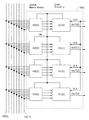
本発明の一態様の電子機器の構成について、図1を用いて説明する。図1は、電子機器に含まれる論理ブロック100aの構成を示す図である。
(Embodiment 1)
A structure of an electronic device of one embodiment of the present invention will be described with reference to FIG. FIG. 1 is a diagram showing a configuration of a
図1に示す論理ブロック100aは、複数のロジックエレメント(ロジックエレメント101[0]乃至ロジックエレメント101[4])、複数のスイッチマトリクスアレイ(スイッチマトリクスアレイ102[0]乃至スイッチマトリクスアレイ102[4])、複数の配線(配線103[0]乃至配線103[7])を有する。
The
配線103[0]乃至配線103[7]を伝送する信号は、スイッチマトリクスアレイ102[0]乃至スイッチマトリクスアレイ102[4]を経由して、ロジックエレメント101[0]乃至ロジックエレメント101[4]に入力可能である。図1の例では、各スイッチマトリクスアレイ102には、8つの配線103の信号を入力可能であり、各スイッチマトリクスアレイ102に記憶されているコンフィギュレーションデータおよび実行中のコンテキストにより、そのうちの4つまでの信号が選択され、対応するロジックエレメント101に配線104を介して供給される。例えば、ロジックエレメント101[1]には、配線104[1−0]乃至配線104[1−3]を介して、信号が入力される。
The signals transmitted through the wirings 103[0] to 103[7] are passed through the switch matrix arrays 102[0] to 102[4] and the logic elements 101[0] to 101[4]. Can be entered in. In the example of FIG. 1, signals of eight
ロジックエレメント101では、記憶されているコンフィギュレーションデータおよび実行中のコンテキスト、あるいはクロック信号CLK等に応じて演算処理がなされ、結果が出力される。ここでは、ロジックエレメント101[1]乃至ロジックエレメント101[4]は演算結果を出力信号OUT[1]乃至出力信号OUT[4]として、配線105[1]乃至配線105[4]に出力する。図示されていないが、出力信号OUT[1]乃至出力信号OUT[4]は、スイッチマトリクスアレイ102(図示されていないものも含む)を介してロジックエレメント101(図示されていないものも含む)に供給されうる。出力信号OUT[1]乃至出力信号OUT[4]が、間接的に配線103[0]乃至配線103[7]に供給されることも可能である。また、ロジックエレメント101からの出力信号OUTは2以上の配線に出力されてもよい。
The
これとは別に、ロジックエレメント101[0]でも同様に演算処理がなされるのであるが、出力(コンテキスト選択信号)は、配線105[0]を介して、ロジックエレメント101[1]乃至ロジックエレメント101[4]、スイッチマトリクスアレイ102[1]乃至スイッチマトリクスアレイ102[4]に供給される。そして、ロジックエレメント101[1]乃至ロジックエレメント101[4]、スイッチマトリクスアレイ102[1]乃至スイッチマトリクスアレイ102[4]では、配線105[0]を介して受け取ったコンテキスト選択信号に応じて、コンフィギュレーションを変更し、指示されたコンテキストを実行する。
Separately from this, the logic element 101[0] is similarly processed, but the output (context selection signal) is output through the wiring 105[0] through the logic element 101[1] to the
図1の論理ブロック100aで、複数のコンテキストを実行する例を説明する。ここでは、演算Aに引き続いて演算Bが実行される例を示す。すなわち、演算AはコンテキストAとして、演算BはコンテキストBとして、それぞれ実行される。したがって、演算Aが終了すると、コンテキストを変更する必要がある。
An example of executing a plurality of contexts in the
ここでは、演算Aが終了すると、配線103[0]の電位がL(ロー)に、配線103[1]の電位がH(ハイ)になるものとする。例えば、いずれかのロジックエレメント101(図示されていないものも含む)あるいは入力端子(図示されていない)から、そのような信号が供給されるように設計あるいは設定される。 Here, when the operation A is completed, the potential of the wiring 103[0] becomes L (low) and the potential of the wiring 103[1] becomes H (high). For example, it is designed or set so that such a signal is supplied from any logic element 101 (including one not shown) or an input terminal (not shown).
コンテキスト選択信号は、ロジックエレメント101[0]で生成され、配線105[0]に出力される。例えば、(演算Aを実行するための)コンテキストAが選択されるときには、配線105[0]の電位はLとなるようにし、(演算Bを実行するための)コンテキストBが選択されるときには、配線105[0]の電位はHとなるように設定する。 The context selection signal is generated by the logic element 101[0] and output to the wiring 105[0]. For example, when the context A (for performing the operation A) is selected, the potential of the wiring 105[0] is set to L, and when the context B (for performing the operation B) is selected, The potential of the wiring 105[0] is set to H.
例えば、スイッチマトリクスアレイ102[0]は、少なくとも配線103[0]と配線103[1]の信号をロジックエレメント101[0]に供給するよう設定される。もちろん、スイッチマトリクスアレイ102[0]は、これらの配線以外の信号もロジックエレメント101[0]に供給するよう設定されてもよい。 For example, the switch matrix array 102[0] is set so as to supply at least signals of the wiring 103[0] and the wiring 103[1] to the logic element 101[0]. Of course, the switch matrix array 102[0] may be set to supply signals other than these wirings to the logic element 101[0].
ただし、ロジックエレメント101[0]では、配線103[0]の電位がLで配線103[1]の電位がH(演算Aが終了したことを意味する)であれば、(ロジックエレメント101[0]に入力されるその他の信号に関わらず)配線105[0]にHを出力し、配線103[0]と配線103[1]の電位がこれら以外の場合には、(ロジックエレメント101[0]に入力されるその他の信号に関わらず)配線105[0]にLを出力するように設定される。 However, in the logic element 101[0], if the potential of the wiring 103[0] is L and the potential of the wiring 103[1] is H (meaning that the operation A is completed), (the logic element 101[0] H is output to the wiring 105[0] regardless of other signals input to the wiring], and when the potentials of the wiring 103[0] and the wiring 103[1] are other than these, (the logic element 101[0] ] Is set to output L to the wiring 105 [0].
配線105[0]の電位は、演算Aが終了していない状態では、Lである。ロジックエレメント101[1]乃至ロジックエレメント101[4]、スイッチマトリクスアレイ102[1]乃至スイッチマトリクスアレイ102[4]は、コンテキストAに設定されている。演算Aが終了し、配線105[0]の電位がHとなると、ロジックエレメント101[1]乃至ロジックエレメント101[4]、スイッチマトリクスアレイ102[1]乃至スイッチマトリクスアレイ102[4]は、コンテキストBに設定が変更され、演算Bが実行される。 The potential of the wiring 105[0] is L when the calculation A is not completed. The logic elements 101[1] to 101[4] and the switch matrix arrays 102[1] to 102[4] are set to the context A. When the operation A is completed and the potential of the wiring 105[0] becomes H, the logic element 101[1] to the logic element 101[4], the switch matrix array 102[1] to the switch matrix array 102[4] are changed to the context. The setting is changed to B, and the calculation B is executed.
このように、コンテキストを切り替えるための信号がローカルに生成されるため、コンテキストの切り替えが極めて高速で実行できる。例えば、1クロック程度の時間で切り替えを完了できる。 In this way, since the signal for switching contexts is locally generated, context switching can be executed at extremely high speed. For example, switching can be completed in about one clock.
図2には他の例を示す。図2に示す論理ブロック100bは、2つのロジックエレメント101[0]とロジックエレメント101[1]の出力信号が2ビットのコンテキスト選択信号となる点で図1に示す論理ブロック100aと異なる。すなわち、ロジックエレメント101[0]の出力信号とロジックエレメント101[1]の出力信号は、それぞれ、配線105[0]と配線105[1]に供給される。
FIG. 2 shows another example. The
ロジックエレメント101[2]乃至ロジックエレメント101[4]、スイッチマトリクスアレイ102[2]乃至スイッチマトリクスアレイ102[4]では、2ビットのコンテキスト選択信号に応じて、コンテキストを選択できる。すなわち、最大で4つのコンテキストを選択できる。同様に、コンテキスト選択信号を供給するロジックエレメント101を増やせば、それに応じてコンテキスト選択信号のビット数を高めることができ、選択できるコンテキスト数も増加する。
In the logic elements 101[2] to 101[4] and the switch matrix arrays 102[2] to 102[4], contexts can be selected according to a 2-bit context selection signal. That is, up to four contexts can be selected. Similarly, if the number of
同様なことは、コンテキスト選択信号を生成するロジックエレメント101の複数の配線から信号が出力されることでも実行できる。例えば、ロジックエレメント101[0]が2本の配線にそれぞれ1ビットの信号を出力することで、上記と同じく、2ビットのコンテキスト選択信号を出力できる。
The same thing can be performed by outputting signals from a plurality of wirings of the
図2の論理ブロック100bでは、最大4つのコンテキストを選択できるので、演算A、演算B、演算C、演算Dを順におこなうとすれば、例えば、演算Aをおこなうときは、配線103[0]と配線103[1]の電位がともにL、演算Bをおこなうときは、配線103[0]の電位がL、配線103[1]の電位がH、演算Cをおこなうときは、配線103[0]の電位がH、配線103[1]の電位がL、演算Dをおこなうときは、配線103[0]と配線103[1]の電位がともにH、となるように設定する。
Since up to four contexts can be selected in the
そして、例えば、ロジックエレメント101[0]は、配線103[0]の信号がLであれば、配線105[0]にLを出力し、配線103[0]の信号がHであれば、配線105[0]にHを出力するように設定される。また、ロジックエレメント101[1]は、配線103[1]の信号がLであれば、配線105[1]にLを出力し、配線103[1]の信号がHであれば、配線105[1]にHを出力するように設定される。 Then, for example, the logic element 101[0] outputs L to the wiring 105[0] if the signal of the wiring 103[0] is L, and outputs the signal to the wiring 103[0] if it is H. It is set to output H to 105[0]. In addition, the logic element 101[1] outputs L to the wiring 105[1] if the signal of the wiring 103[1] is L, and outputs L to the wiring 105[1] if the signal of the wiring 103[1] is H. 1] is set to output H.
配線105[0]と配線105[1]の信号は、ロジックエレメント101[2]乃至ロジックエレメント101[4]、スイッチマトリクスアレイ102[2]乃至スイッチマトリクスアレイ102[4]でデコードされ、デコードされた信号に基づいて、ロジックエレメント101[2]乃至ロジックエレメント101[4]、スイッチマトリクスアレイ102[2]乃至スイッチマトリクスアレイ102[4]のコンテキストが変更される。 The signals of the wirings 105[0] and 105[1] are decoded and decoded by the logic element 101[2] to the logic element 101[4] and the switch matrix array 102[2] to the switch matrix array 102[4]. The contexts of the logic elements 101[2] to 101[4] and the switch matrix arrays 102[2] to 102[4] are changed based on the signals.
図1や図2の例では、コンテキスト選択信号を生成するロジックエレメント101が固定されていたが、例えば、図3に示すように、ロジックエレメント101[0]乃至ロジックエレメント101[3]のいずれかがコンテキスト選択信号を生成する構成でもよい。
Although the
図3に示す論理ブロック100cでは、ロジックエレメント101[0]乃至ロジックエレメント101[3]のそれぞれは、演算結果を出力信号OUT[0]乃至出力信号OUT[3]として出力するか、コンテキスト選択信号として、コンテキスト選択信号線106に出力する。
In the
具体的には、ロジックエレメント101[0]乃至ロジックエレメント101[3]のいずれか一がコンテキスト選択信号を生成し、コンテキスト選択信号線106にコンテキスト選択信号を出力する。なお、コンテキスト選択信号が2ビット以上の場合には、ロジックエレメント101[0]乃至ロジックエレメント101[3]の複数がコンテキスト選択信号を出力し、また、コンテキスト選択信号線106はコンテキスト選択信号のビット数に応じて複数存在する。あるいは、ロジックエレメント101[0]乃至ロジックエレメント101[3]のいずれか一が、2ビット以上のコンテキスト選択信号を、ビット数に応じた数のコンテキスト選択信号線106に出力すればよい。
Specifically, one of the logic elements 101[0] to 101[3] generates a context selection signal and outputs the context selection signal to the context
また、コンテキスト選択信号を生成するロジックエレメント101は、コンテキスト選択信号線106からの信号を受け取らないように設計あるいは設定される。あるいは、コンテキスト選択信号線106からの信号を受け取るように設計されている場合には、コンテキスト選択信号に関わらず、同じコンフィギュレーションを維持するようなコンフィギュレーションデータが入力されていてもよい。
Further, the
ロジックエレメント101[0]乃至ロジックエレメント101[3]のその他は、コンテキスト選択信号を出力しない。さらに、コンテキスト選択信号線106からの信号を受け取るように設計あるいは設定される。すなわち、コンテキスト選択信号を出力するか否かで、ロジックエレメント101の回路構成や論理構成を設定すればよい。
The other logic elements 101[0] to 101[3] do not output the context selection signal. Further, it is designed or set to receive a signal from the context
図3に示すような構成によって、ロジックエレメント101への入力信号線の数が4から5に増えたものと同様の効果があり、ロジックエレメント101でより複雑な演算ができるが、その一方で、入力信号線の接続先が限定されることによりレイアウト面積の増大が抑制される。
With the configuration as shown in FIG. 3, the same effect as that in which the number of input signal lines to the
図3に示す論理ブロック100cでは、コンテキスト選択信号を受け入れる端子と出力する端子が異なるように表現されている。しかし、実際の回路では、1つの端子の機能を入力にも出力にも使用できる。例えば、図4のような回路を構成してもよい。
In the
図4に示す論理ブロック100dでは、それぞれのロジックエレメント101は、コンテキスト選択信号線106と1つの端子で接続されているように表現されている。そして、コンテキスト選択信号を受け入れるか出力するかは、内部の回路構成によって決定できる。具体例はロジックエレメント101の構成例として後述される。
In the
以上の例では、コンテキスト選択信号は、配線103を伝送する信号のみから生成されるが、その他の信号から生成されてもよい。例えば、一以上の配線103を伝送する信号とクロック信号とから生成されてもよい。
In the above example, the context selection signal is generated only from the signal transmitted through the
スイッチマトリクスアレイ102の例を図5に示す。図5に示されるスイッチマトリクスアレイ102[1]は、配線103[0]乃至配線103[7]および配線104[1−1]乃至配線104[1−4]に重なるように設けられる。配線104[1−1]乃至配線104[1−4]は、ロジックエレメント101[1]に信号を供給する。
An example of the
スイッチマトリクスアレイ102[1]は、マトリクス状に配置された、複数のスイッチ回路107を有する。各スイッチ回路107は対応する配線103と配線104の電気的な接続や切断を受け持つ。例えば、スイッチ回路107[1−0,1]は、配線103[1]と配線104[1−0]との間の電気的な接続や切断を受け持ち、スイッチ回路107[1−3,7]は、配線103[7]と配線104[1−3]との間の電気的な接続や切断を受け持つ。スイッチ回路107の動作は、配線105[0](あるいはコンテキスト選択信号線106)を伝送するコンテキスト選択信号に応じて変更できる。
The switch matrix array 102[1] has a plurality of switch circuits 107 arranged in a matrix. Each switch circuit 107 takes charge of electrical connection and disconnection between the
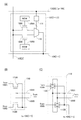
配線103[2]と配線104[1−1]との間の電気的な接続や切断を受け持つスイッチ回路107[1−1,2]は、例えば、図6(A)に示されるように、パストランジスタ108Aとパストランジスタ108B、メモリ109Aとメモリ109B、2入力のマルチプレクサ110、デコーダ111を有する。図6(A)に示されるスイッチ回路107[1−1,2]では、2つのコンテキスト(コンテキストAとコンテキストB)のいずれかを選択し、実行できる。デコーダ111からは、1以上の配線を介してマルチプレクサ110に信号が供給される。
The switch circuit 107[1-1,2] responsible for electrical connection and disconnection between the wiring 103[2] and the wiring 104[1-1] is, for example, as shown in FIG. It includes a
マルチプレクサ110は、例えば、図6(B)に示すような、選択トランジスタ112Aと選択トランジスタ112Bを有する回路で表現できる。あるいは、図6(C)に示すように、相互に異なる動きをする1対のトランスファーゲート(トランスファーゲート113Aとトランスファーゲート113B)を用いても表現できる。なお、これらの例では、デコーダ111からの2本の配線(制御信号線105A、制御信号線105B)によって、選択トランジスタ112Aと選択トランジスタ112Bやトランスファーゲート113Aとトランスファーゲート113Bが制御される。
The
配線105[0](あるいはコンテキスト選択信号線106)を伝送する信号は、デコーダ111でデコードされ、デコーダ111は、コンテキスト選択信号に応じて、制御信号線105Aと制御信号線105Bのいずれか一方がH、他方がLとなるような電位を制御信号線105Aと制御信号線105Bに供給する。
A signal transmitted through the wiring 105[0] (or the context selection signal line 106) is decoded by the
例えば、配線105[0]の電位がLであれば、制御信号線105Aの電位がH、制御信号線105Bの電位がLとなり、配線105[0]の電位がHであれば、制御信号線105Aの電位がL、制御信号線105Bの電位がHとなるような電位が、デコーダ111から供給される。
For example, if the potential of the wiring 105[0] is L, the potential of the
図6(C)のように、トランスファーゲート113Aとトランスファーゲート113Bを用いる場合は、制御信号線105Aと制御信号線105Bの電位が上記のような関係にあると以下の点で有利である。
When the
すなわち、1つのトランスファーゲートには、制御のためにHとLの双方の信号を入力するが、デコーダ111からは、常にHとLの双方の信号が出力されている。したがって、それらの電位をトランスファーゲート113Aとトランスファーゲート113Bの制御に用いることができるので、より高速な動作が可能である。
That is, both H and L signals are input to one transfer gate for control, but both H and L signals are always output from the
パストランジスタ108Aとパストランジスタ108Bは、それぞれ、メモリ109Aとメモリ109Bの出力(これはそれぞれに記憶されている1ビットデータと等価である)によって、導通が制御される。
The conduction of the
マルチプレクサ110として、図6(B)に示す回路を採用した場合、パストランジスタ108Aのソースとドレインは、配線103[2]と選択トランジスタ112Aのソース(あるいはドレイン)の間にあるような回路構成であるが、選択トランジスタ112Aのソースとドレインが、配線103[2]とパストランジスタ108Aのソース(あるいはドレイン)の間にあるように回路を設計してもよい。図6(C)に示す回路を採用した場合でも同様である。
When the circuit shown in FIG. 6B is adopted as the
図7(A)には、変形例を示す。図7(A)に示すスイッチ回路107[1−1,2]では、メモリ109Aとメモリ109Bの出力信号がマルチプレクサ110で選択され、それがパストランジスタ108のゲートに入力される構成を有する。マルチプレクサ110は、図6(A)の場合と同様に、デコーダ111の出力信号により制御される。
A modified example is shown in FIG. The switch circuit 107 [1-1, 2] illustrated in FIG. 7A has a structure in which output signals of the
図7(B)には、他の変形例を示す。図7(B)に示すスイッチ回路107[1−1,2]では、メモリ109Aとメモリ109Bの動作が制御信号線105A、制御信号線105Bを伝送するデコーダ111の出力信号により制御される。例えば、制御信号線105Aには、メモリ109Aの動作を有効にする信号が、制御信号線105Bには、メモリ109Bの動作を無効にする信号が供給される。
FIG. 7B shows another modification. In the switch circuit 107 [1-1, 2] illustrated in FIG. 7B, operations of the
以上は、コンテキスト選択信号が1ビットの場合であるが、2ビット以上に適用するには、図6(A)あるいは図7(A)のマルチプレクサの入力端子数を増加させればよい。あるいは、図6(B)、図6(C)あるいは図7(B)において、3以上の制御信号線を介して、その配線の数に見合うトランジスタやトランスファーゲート、メモリ等にデコーダ111から制御信号が供給されてもよい。
The above is the case where the context selection signal is 1 bit, but in order to apply it to 2 bits or more, the number of input terminals of the multiplexer in FIG. 6A or FIG. 7A may be increased. Alternatively, in FIG. 6B, FIG. 6C, or FIG. 7B, the control signal from the
例えば、コンテキスト選択信号が2ビットの場合を図8に示す。ここで、スイッチ回路107[1−1,2]は、パストランジスタ108A乃至パストランジスタ108D、メモリ109A乃至メモリ109D、選択トランジスタ112A乃至選択トランジスタ112Dを有し、パストランジスタ108Aと選択トランジスタ112Aが、配線103[2]と配線104[1−1]の間に直列にあるように回路が設計される。選択トランジスタ112A乃至選択トランジスタ112Dの代わりにトランスファーゲートあるいはそれと同等な機能を有する回路を用いてもよい。
For example, FIG. 8 shows a case where the context selection signal has 2 bits. Here, the switch circuit 107 [1-1, 2] includes the
配線105[0]と配線105[1]を伝送する2ビットのコンテキスト選択信号は、デコーダ111でデコードされ、制御信号線105A乃至制御信号線105Dのいずれか一のみがH、他がLとなるような電位が、制御信号線105A乃至制御信号線105Dに供給される。選択トランジスタ112A乃至選択トランジスタ112Dは、制御信号線105A乃至制御信号線105Dの電位に応じ、いずれか一のみがオンとなり、他はオフとなる。
The 2-bit context selection signal transmitted through the wirings 105[0] and 105[1] is decoded by the
デコーダ111は、例えば、図9(A)に示すように、インバータ114a乃至インバータ114cを有する。なお、インバータ114bとインバータ114cを設けない構造でもよい。あるいは、インバータ114aに直列に、さらに2個のインバータを追加してもよい。つまり、配線105[0]がデコーダ111内で分岐したあと、制御信号線105Aにつながる配線に設けられるインバータの数(0を含む)と制御信号線105Bにつながる配線に設けられるインバータの数(0を含む)の差が奇数となるような回路であればよい。この結果、制御信号線105Aと制御信号線105Bの電位は、一方がHであれば他方がLとなる。
The
また、別の例では、図9(B)に示すように、デコーダ111は、1入力のデマルチプレクサ115を有する。デマルチプレクサ115は、配線105[0]の電位に応じて、一方がHであれば他方がLとなるような電位を制御信号線105Aと制御信号線105Bに供給する。また、別の例では、図9(C)に示すように、デコーダ111は、2入力のデマルチプレクサ115を有する。デマルチプレクサ115は、配線105[0]の電位と配線105[1]の電位に応じて、いずれか一のみがHで、他がLとなるような電位を制御信号線105A乃至制御信号線105Dに供給する。
In another example, as shown in FIG. 9B, the
以上の例では、コンテキスト選択信号は、ロジックエレメント101とスイッチマトリクスアレイ102の双方に入力されたが、いずれか一方にのみ入力される構成でもよい。また、デコーダ111は、ロジックエレメント101と対応するスイッチマトリクスアレイ102の双方に、それぞれ、設けられてもよいし、いずれか一方にのみ設けて、デコーダ111の出力信号(制御信号)が他方にも供給されるようにしてもよい。あるいは、デコーダ111を複数のロジックエレメント101、複数のスイッチマトリクスアレイ102に1つの割合で設けて、デコーダの設けられていないものに制御信号を供給してもよい。
In the above example, the context selection signal is input to both the
次に、ロジックエレメント101について説明する。一般的に、ロジックエレメント101は1以上のルックアップテーブル、1以上のフリップフロップ(FF)、1以上のマルチプレクサ(MUX)を有する。なお、一般にルックアップテーブルはメモリを有する。
Next, the
ルックアップテーブルをロジックゲートとして機能させるために、コンフィギュレーションデータが、ルックアップテーブルに入力される。換言すれば、ルックアップテーブルから出力される信号のロジックレベル(例えば「H/L」)は、コンフィギュレーションデータとルックアップテーブルへ入力される信号のロジックレベルに応じて決定される。 Configuration data is input to the look-up table to cause the look-up table to function as a logic gate. In other words, the logic level (for example, "H/L") of the signal output from the look-up table is determined according to the configuration data and the logic level of the signal input to the look-up table.
ルックアップテーブルから出力される信号はフリップフロップに入力される。ロジックエレメント101に含まれているフリップフロップから出力される信号は、他のロジックエレメント101に含まれているフリップフロップに入力されることがある。フリップフロップはこれらの入力信号を保持する機能を有する。
The signal output from the look-up table is input to the flip-flop. A signal output from a flip-flop included in the
マルチプレクサの駆動を制御するために、コンフィギュレーションデータがマルチプレクサに入力される。マルチプレクサは、コンフィギュレーションデータに応じて、ルックアップテーブルあるいはフリップフロップから出力される信号のいずれかを選択する機能を有する。マルチプレクサによって選択された信号はロジックエレメント101から出力される。
Configuration data is input to the multiplexer to control the driving of the multiplexer. The multiplexer has a function of selecting either the look-up table or the signal output from the flip-flop according to the configuration data. The signal selected by the multiplexer is output from the
また、ルックアップテーブルやマルチプレクサを制御するコンフィギュレーションデータは、コンテキスト選択信号によって、必要なものを選択することができる。 Further, the configuration data for controlling the look-up table and the multiplexer can be selected as required by the context selection signal.
図10(A)はロジックエレメント101の具体的な構成例を示す。図10(A)のロジックエレメント101aは、デコーダ121、マルチプレクサ122、フリップフロップ123、マルチプレクサ124、マルチプレクサ122のためのコンフィギュレーションデータを格納するコンフィギュレーションメモリ125a、マルチプレクサ124のためのコンフィギュレーションデータを格納するコンフィギュレーションメモリ125bを有する。マルチプレクサ122とコンフィギュレーションメモリ125aが上述のルックアップテーブルに相当する。デコーダ121は、図9(A)乃至図9(C)で説明したデコーダ111と同じあるいは同様なものである。
FIG. 10A shows a specific configuration example of the
マルチプレクサ122で実行される論理動作は、コンフィギュレーションメモリ125aに格納されているコンフィギュレーションデータおよびコンテキスト選択信号線106から供給されるコンテキスト選択信号に応じて変わる。コンテキスト選択信号は、デコーダ121でデコードされる。デコーダ121の出力に応じて、コンフィギュレーションメモリ125a、コンフィギュレーションメモリ125bから、マルチプレクサ122、マルチプレクサ124に、それぞれロードされるデータが変化する。
The logic operation executed by the
その結果、マルチプレクサ122は、例えば、一のコンテキストでは、ANDゲートとして動作するが、別のコンテキストでは、ORゲートとして動作する、というように、その機能を変化させることができる。
As a result, the
マルチプレクサ122は、配線104から供給される複数の入力信号に対応した出力信号を生成する。フリップフロップ123は、マルチプレクサ122で生成された出力信号を保持し、クロック信号CLKに同期してマルチプレクサ122の出力信号に対応する出力信号を出力する。
The
マルチプレクサ122およびフリップフロップ123から出力される信号はマルチプレクサ124に入力される。マルチプレクサ124は、コンフィギュレーションメモリ125bに格納されているコンフィギュレーションデータとコンテキスト選択信号に応じてこれら2つの出力信号のうちの一つを選択し、出力する機能を有する。マルチプレクサ124から出力される信号は配線105に供給される。
The signals output from the
図10(B)は、ロジックエレメント101の別の具体的な構成例を示す。図10(B)のロジックエレメント101bは、図10(A)のロジックエレメント101aとマルチプレクサ126とマルチプレクサ126のためのコンフィギュレーションデータを格納するコンフィギュレーションメモリ125cを有する点で異なる。
FIG. 10B shows another specific configuration example of the
マルチプレクサ122から出力される信号と他のロジックエレメント101から出力される信号(配線104から供給される)がマルチプレクサ126に入力される。マルチプレクサ126は、コンフィギュレーションメモリ125cに格納されているコンフィギュレーションデータに応じてこれら2つの信号のうちの一つを選択し、出力する機能を有する。
A signal output from the
図10(B)のロジックエレメント101bでは、フリップフロップ123は、マルチプレクサ126から出力された信号を保持し、クロック信号CLKに同期してマルチプレクサ126から出力された信号に対応する出力信号を出力する。
In the
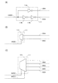
図11(A)には、図4で示される論理ブロック100dに使用するためのロジックエレメント101の例を示す。図11(A)に示すロジックエレメント101cは、図10(A)に示すロジックエレメント101aをベースにしたものである。図11(A)に示すロジックエレメント101cは、マルチプレクサ124の出力が、2出力のデマルチプレクサ127で配線105と2入力のマルチプレクサ128のいずれかに出力される。デマルチプレクサ127としては、図6(B)あるいは図6(C)に示すマルチプレクサ110と同等な回路を用いてもよい。
FIG. 11A shows an example of the
なお、マルチプレクサ128は3つの端子(端子a、端子b、端子c)を有するが、端子aと端子bのうち、端子cと接続していないものには、一定の電位が出力されるものとする。例えば、2つのコンテキストが切り替えられる方式(コンテキスト選択信号が1ビット)で、コンテキスト選択信号の初期値がLである場合には、その一定の電位をLとしてもよい。同様に、デマルチプレクサ127においても、選択されないほうの端子には、電位Lが与えられてもよい。
Note that the
ロジックエレメント101cがコンテキスト選択信号を生成する場合には、マルチプレクサ124の出力(コンテキスト選択信号)はデマルチプレクサ127とマルチプレクサ128を経由してコンテキスト選択信号線106に出力される。すなわち、この場合には、端子bと端子cが接続される。端子aは端子cと接続されないので、端子aにはLの電位が供給される。端子aの出力はデコーダ121でデコードされて、ロジックエレメント101cは初期のコンテキストに維持される。
When the
ロジックエレメント101cがコンテキスト選択信号を生成しない場合には、マルチプレクサ124の出力はデマルチプレクサ127を経由して配線105に出力される。また、コンテキスト選択信号線106とマルチプレクサ128を経由して、コンテキスト選択信号がデコーダ121に入力される。すなわち、この場合には、端子aと端子cが接続される。端子bは端子cと接続されないので、端子bにはLの電位が供給される。
When the
デマルチプレクサ127、マルチプレクサ128の動作は、それぞれ、コンフィギュレーションメモリ125d、コンフィギュレーションメモリ125eに記憶されているコンフィギュレーションデータによって設定されている。
The operations of the
マルチプレクサ128では、コンテキスト選択信号線106が、デコーダ121、デマルチプレクサ127の出力端子のいずれと接続するかが決定される。ここで、コンテキスト選択信号線106がデコーダ121と接続するのであれば、ロジックエレメント101cは、コンテキスト選択信号を受け入れることができる。逆に、コンテキスト選択信号線106がデマルチプレクサ127の出力端子と接続するのであれば、ロジックエレメント101cは、コンテキスト選択信号を出力することができる。
The
なお、ロジックエレメント101cが、コンテキスト選択信号を受け入れるか出力するかのいずれかの状態しかとらないのであれば、コンフィギュレーションメモリ125d、コンフィギュレーションメモリ125eに記憶されているコンフィギュレーションデータは実質的に同じものである(すなわち、一方が他方と全く同じか、全く反対かのいずれかである)ので、コンフィギュレーションメモリ125dとコンフィギュレーションメモリ125eを、1つのコンフィギュレーションメモリと、必要によっては、そのメモリの出力を反転させる回路とで代替することもできる。
Note that if the
なお、マルチプレクサ124の出力が仮にコンテキスト選択信号であったとし、それが配線105に供給されたとしても、その先に存在するスイッチ(スイッチマトリクスアレイ内のスイッチ)によって、他のロジックエレメントが取り込まないようにすることが可能である。その場合には、デマルチプレクサ127は不要である。
Note that if the output of the
そのような構成を有するロジックエレメントの例を図11(B)に示す。図11(B)に示されるロジックエレメント101dは、トライステートバッファー129(あるいは、それと同等な機能を有する回路)と論理ゲート130を有する。論理ゲート130には、2つの信号が入力される。論理ゲート130は、第1の入力にはそのままの信号が、第2の入力には反転された信号が入力される構成のANDゲートと同等である。したがって、論理ゲート130は、第1の入力に反転した信号が、第2の入力にはそのままの信号が入力されるNORゲートとも同等である。
An example of a logic element having such a structure is shown in FIG. The
ロジックエレメント101dにおいて、マルチプレクサ124の出力は、配線105に供給されるとともに、トライステートバッファー129にも供給される。トライステートバッファー129の出力はコンテキスト選択信号線106および論理ゲート130の一方の入力に供給される。論理ゲート130の他方の入力には、コンフィギュレーションメモリ125dの出力が入力される。
In the
トライステートバッファー129は、コンフィギュレーションメモリ125dによって制御され、コンフィギュレーションメモリ125dの出力がHであれば、オンとなり、Lであればオフとなる。ここでは、このロジックエレメント101dが、コンテキスト選択信号を生成する場合には、コンフィギュレーションメモリ125dの出力がH、そうでない場合には、Lであるとする。
The
例えば、コンフィギュレーションメモリ125dの出力がHの場合、トライステートバッファー129がオンであるので、配線105とコンテキスト選択信号線106と論理ゲート130の一方の入力には、マルチプレクサ124の出力(コンテキスト選択信号)が供給される。トライステートバッファー129の出力は、HかLか不明であるが、論理ゲート130の他方の入力にはHが入力されるので、論理ゲート130は常にLを出力する。したがって、トライステートバッファー129の出力によってコンテキストが変更されることはない。
For example, when the output of the
例えば、コンフィギュレーションメモリ125dの出力がLの場合、トライステートバッファー129がオフであるので、配線105にのみ、マルチプレクサ124の出力が供給される。また、コンテキスト選択信号線106を介して、他のロジックエレメントからコンテキスト選択信号が、論理ゲート130の一方の入力に供給される。論理ゲート130の他方の入力には、コンフィギュレーションメモリ125dの出力(L)が供給されるので、論理ゲート130は、コンテキスト選択信号線106の電位がHであればHを、LであればLを出力する。
For example, when the output of the
図11(B)のコンフィギュレーションメモリ125d、トライステートバッファー129、論理ゲート130の機能は、他の論理ゲートでも実現できる。例えば、第1乃至第4の端子を有し、第1の状態では、第1の端子と第3の端子が、第2の端子と第4の端子に、それぞれ接続され、第2の状態では、第1の端子が第4の端子と接続され、第3の端子と第2の端子は、他のいずれの端子とも接続されない論理ゲートでもよい。この場合、例えば、第1の端子とデコーダ121の入力とを接続し、第3の端子とマルチプレクサ124の出力とを接続し、第2の端子の電位をLとし、第4の端子とコンテキスト選択信号線106とを接続する。
The functions of the
第1の状態では、デコーダ121の入力の電位はLとなり、マルチプレクサ124の出力はコンテキスト選択信号線106と接続される。第2の状態では、コンテキスト選択信号線106はデコーダ121の入力と接続される。マルチプレクサ124の出力は、第2の端子、第4の端子とも接続されないが、配線105とは第1の状態でも第2の状態でも接続されている。
In the first state, the potential of the input of the
すなわち、第1の状態では、ロジックエレメントで生成したコンテキスト選択信号をコンテキスト選択信号線106に供給することが可能であり、第2の状態では、他のロジックエレメントで生成されたコンテキスト選択信号を受け入れて、コンテキストを変更し、演算結果を配線105に出力できる。
That is, in the first state, the context selection signal generated by the logic element can be supplied to the context
なお、図10(A)、図10(B)、図11(A)あるいは図11(B)に示されるロジックエレメント101では、コンフィギュレーションデータによって使用可能なフリップフロップ123の型が決定される。特に、フリップフロップ123は、コンフィギュレーションデータにもよるが、D−フリップフロップ、T−フリップフロップ、JK−フリップフロップ、RS−フリップフロップのいずれかである。
In the
電子装置は、上記のような論理ブロック100a乃至論理ブロック100d、あるいはそれらと同等な機能を有するもの(これらを論理ブロック100、という)のいずれか1あるいは2以上を複数組み合わせて用いられる。図12に示す例では、論理ブロック100[0]の出力信号が配線103[0]乃至配線103[7]に供給される。論理ブロック100[1]には、配線103[0]乃至配線103[7]を伝送する信号が供給され、論理ブロック100[1]の出力信号は配線103[8]乃至配線103[15]に供給される。論理ブロック100[2]には、配線103[8]乃至配線103[15]を伝送する信号が供給され、論理ブロック100[2]の出力信号は配線103[16]乃至配線103[23]に供給される。論理ブロック100[3]には、配線103[16]乃至配線103[23]を伝送する信号が供給される。
The electronic device is used by combining any one or more of the
図12のような構成を有する電子装置の駆動例を説明する。論理ブロック100[0]は、配線103[0]と配線103[1]にコンテキスト選択信号を生成するための電位を供給し、配線103[2]乃至配線103[7]に演算に使用するためのデータを供給するとする。例えば、論理ブロック100[0]は、シリアルな信号列を解析して、ヘッダーを見つけ出し、ヘッダーの直後にあるコンテキスト選択信号を生成するための2ビットのデータ(コンテキスト決定データ)を抽出する機能を有する。そして、コンテキスト決定データに応じた電位を配線103[0]と配線103[1]に供給する。また、論理ブロック100[0]は、コンテキスト決定データに続く6ビットのデータを配線103[2]乃至配線103[7]に供給する。コンテキスト決定データは上記のようなHとLの組み合わせである。 A driving example of the electronic device having the configuration shown in FIG. 12 will be described. The logic block 100[0] supplies a potential for generating a context selection signal to the wiring 103[0] and the wiring 103[1] and is used for calculation in the wirings 103[2] to 103[7]. Of data. For example, the logic block 100[0] has a function of analyzing a serial signal sequence to find a header, and extracting 2-bit data (context decision data) for generating a context selection signal immediately after the header. Have. Then, a potential corresponding to the context determination data is supplied to the wiring 103[0] and the wiring 103[1]. Further, the logic block 100[0] supplies 6-bit data following the context determination data to the wirings 103[2] to 103[7]. The context determination data is a combination of H and L as described above.
論理ブロック100[1]では、配線103[0]と配線103[1]の電位に基づいて、コンテキスト選択信号が生成され、論理ブロック100[1]内のコンテキストが変更される。そして、配線103[2]乃至配線103[7]の電位をもとに、演算がおこなわれ、配線103[8]乃至配線103[15]に、演算結果が出力される。ここで、演算結果は、2ビットのコンテキスト決定データと、次の演算に使用するための6ビットのデータよりなり、コンテキスト決定データは、配線103[8]と配線103[9]に出力され、その他のデータは、配線103[10]乃至配線103[15]に出力される。このように、一の演算結果の中にコンテキスト決定データが含まれるようにすることで、次の論理ブロックでコンテキストが変更され、別の演算がなされる。そして、この例では、論理ブロック100[1]の出力が変化すると、それに応じてコンテキストも変化する。 In the logic block 100[1], a context selection signal is generated based on the potentials of the wiring 103[0] and the wiring 103[1], and the context in the logic block 100[1] is changed. Then, calculation is performed based on the potentials of the wirings 103[2] to 103[7], and the calculation result is output to the wirings 103[8] to 103[15]. Here, the operation result is composed of 2-bit context determination data and 6-bit data to be used in the next operation, and the context determination data is output to the wiring 103[8] and the wiring 103[9]. The other data is output to the wirings 103[10] to 103[15]. In this way, by including the context determination data in one operation result, the context is changed in the next logical block and another operation is performed. Then, in this example, when the output of the logic block 100[1] changes, the context also changes accordingly.
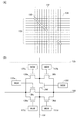
他の例を図13に示す。図13に示される電子装置は、論理ブロック100がマトリクス状に配置されている。例えば、論理ブロック100[0,0]は、配線群132[0]から信号が供給され、配線群132[1]に出力する。また、配線群132[0]には、出入力回路131[0]から信号が供給される。配線群132は、複数の配線103から構成され、ここでは、1つの配線群132は、32本の配線103よりなる(すなわち、配線群132は32ビットである)とする。また、1つの論理ブロック100は8ビットのデータを出力できる(すなわち、1つの論理ブロック100から外部に出力できる配線105が8本ある)とする。
Another example is shown in FIG. In the electronic device shown in FIG. 13, logic blocks 100 are arranged in a matrix. For example, the logic block 100[0,0] is supplied with a signal from the wiring group 132[0] and outputs the signal to the wiring group 132[1]. A signal is supplied from the input/output circuit 131[0] to the wiring group 132[0]. The
例えば、配線群132[0]には、出入力回路131[0]から、シリアルな信号列が順次、入力される。この信号列には、6ビット乃至32ビットのヘッダーと、それに続く2ビットのコンテキスト決定データと、演算に使用する16乃至30ビットのデータが含まれているとする。このようにヘッダーやデータのビット数は可変でもよい。 For example, a serial signal string is sequentially input to the wiring group 132[0] from the input/output circuit 131[0]. It is assumed that this signal string includes a 6-bit to 32-bit header, a 2-bit context determination data following the header, and 16 to 30-bit data used for the operation. As described above, the number of bits of the header or data may be variable.
左の8つの論理ブロック100、すなわち、論理ブロック100[0,0]乃至論理ブロック100[3,1]は、ヘッダーを見つけ出し、それに続くコンテキスト決定データ(第1のコンテキスト決定データ)と演算に使用するデータを配線群132[2]に供給する。
The eight
論理ブロック100[0,2]乃至論理ブロック100[3,2]では、第1のコンテキスト決定データによって、用いるコンテキストが決定され、これと演算に使用するデータを用いて演算がおこなわれる。ここで、論理ブロック100[0,2]乃至論理ブロック100[2,2]は、2ビットの第2のコンテキスト決定データと16ビットのデータを、論理ブロック100[3,2]は、2ビットの第3のコンテキスト決定データと4ビットのデータを配線群132[3]に供給するものとする。また、これとは別に、出入力回路131[3]が8ビットのデータを配線群132[3]に供給するものとする。 In the logic blocks 100[0,2] to the logic blocks 100[3,2], the context to be used is determined by the first context determination data, and the operation is performed using this and the data used for the operation. Here, the logical block 100[0,2] to the logical block 100[2,2] are provided with 2-bit second context determination data and 16-bit data, and the logical block 100[3,2] is provided with 2-bit. 3rd context determination data and 4-bit data are supplied to the wiring group 132[3]. Separately from this, the input/output circuit 131[3] supplies 8-bit data to the wiring group 132[3].
例えば、配線群132[3]は、配線103[3−0]乃至配線103[3−31]よりなるものとする。ここで、論理ブロック100[0,2]、論理ブロック100[1,2]、論理ブロック100[2,2]、論理ブロック100[3,2]は、それぞれ、配線103[3−0]乃至配線103[3−7]、配線103[3−8]乃至配線103[3−15]、配線103[3−16]乃至配線103[3−23]、配線103[3−24]乃至配線103[3−31]に信号を出力可能であるとする。出入力回路131[3]は、配線103[3−0]乃至配線103[3−31]すべてに信号を供給できるものとする。
For example, the wiring group 132[3] includes the wiring 103[3-0] to the wiring 103[3-31]. Here, the logical block 100[0,2], the logical block 100[1,2], the logical block 100[2,2], and the logical block 100[3,2] are respectively connected to the wirings 103[3-0] to 103[3-0]. Wiring 103[3-7], Wiring 103[3-8] to Wiring 103[3-15], Wiring 103[3-16] to Wiring 103[3-23], Wiring 103[3-24] to
そして、第2のコンテキスト決定データは配線103[3−0]と配線103[3−1]に、16ビットのデータは配線103[3−2]乃至配線103[3−17]に、第3のコンテキスト決定データは配線103[3−26]と配線103[3−27]に、4ビットのデータは、配線103[3−28]乃至配線103[3−31]に、出入力回路131[3]が供給する8ビットのデータは配線103[3−18]乃至配線103[3−25]に、それぞれ供給されるとする。 The second context determination data is stored in the wiring 103[3-0] and the wiring 103[3-1], and the 16-bit data is stored in the wiring 103[3-2] to the wiring 103[3-17]. Of the input/output circuit 131[] to the wiring 103[3-26] and the wiring 103[3-27], and 4-bit data to the wiring 103[3-28] to the wiring 103[3-31]. The 8-bit data supplied by [3] is supplied to the wirings 103[3-18] to 103[3-25], respectively.
そして、論理ブロック100[0,3]乃至論理ブロック100[2,3]のそれぞれは、配線群132[3]のうちの2本の配線(配線103[3−0]と配線103[3−1])から第2のコンテキスト決定データを読み出し、それに付随するデータを用いて第1のコンテキストを実行する。つまり、論理ブロック100[0,3]乃至論理ブロック100[2,3]のそれぞれにおいて、コンテキスト選択信号を生成するロジックエレメント101(これらの論理ブロック100には、計3つ存在する)に、第2のコンテキスト決定データが供給されるように、対応するスイッチマトリクスアレイ102は、いずれも、配線103[3−0]と配線103[3−1]が、コンテキスト選択信号を生成するロジックエレメント101に電気的に接続するように設定されている。
Each of the logic block 100[0,3] to the logic block 100[2,3] has two wirings (wiring 103[3-0] and wiring 103[3-] in the wiring group 132[3]. 1]), the second context determination data is read out, and the first context is executed by using the data accompanying it. That is, in each of the logic blocks 100[0,3] to 100[2,3], the
なお、演算に用いるデータは、論理ブロック100[0,2]乃至論理ブロック100[2,2]が供給する16ビットのデータと、出入力回路131[3]が供給する8ビットのデータの一部(例えば、4ビットのデータ)である。 Note that the data used for the operation is one of 16-bit data supplied by the logic block 100[0,2] to logic block 100[2,2] and 8-bit data supplied by the input/output circuit 131[3]. Part (for example, 4-bit data).
一方、論理ブロック100[3,3]は、配線群132[3]のうちの別の2本の配線(配線103[3−26]と配線103[3−27])から第3のコンテキスト決定データを読み出し、それに付随するデータを用いて第2のコンテキストを実行する。このように、1つの電子機器の中で、同時に異なる領域で異なるコンテキストが実行される。また、コンテキストを実行する領域もユーザーが設定できる。 On the other hand, the logic block 100[3,3] determines the third context from another two wirings (wiring 103[3-26] and wiring 103[3-27]) of the wiring group 132[3]. Read the data and use the data associated with it to execute the second context. In this way, different contexts are simultaneously executed in different areas within one electronic device. The user can also set the area in which the context is executed.
別の例では、論理ブロック100[0,2]が、第2のコンテキスト決定データと第3のコンテキスト決定データを供給することも可能である。この場合、第2のコンテキスト決定データと第3のコンテキスト決定データは、配線103[3−0]乃至配線103[3−7]のいずれかに供給される。 In another example, logic block 100[0,2] could provide the second context decision data and the third context decision data. In this case, the second context determination data and the third context determination data are supplied to any of the wirings 103[3-0] to 103[3-7].
上記において、第1のコンテキスト決定データ、第2のコンテキスト決定データ、第3のコンテキスト決定データは、互いに独立である。例えば、第1のコンテキスト決定データと第2のコンテキスト決定データは常に同じであるとは限らないし、常に異なるとも限らない。第1のコンテキスト決定データがある2ビットの値であるとき、必ず、第2のコンテキスト決定データが特定の2ビットの値となるわけではない。第1のコンテキスト決定データと第3のコンテキスト決定データでも同様である。また、これらから得られ、ロジックエレメント101から出力されるコンテキスト選択信号もそれぞれ互いに独立である。
In the above, the first context determination data, the second context determination data, and the third context determination data are independent of each other. For example, the first context determination data and the second context determination data are not always the same or always different. When the first context determination data has a certain 2-bit value, the second context determination data does not always have a specific 2-bit value. The same applies to the first context determination data and the third context determination data. Further, the context selection signals obtained from them and output from the
例えば、第2のコンテキスト決定データと第3のコンテキスト決定データは、論理ブロック100[0,2]乃至論理ブロック100[3,2]で実行された演算結果を反映する。 For example, the second context determination data and the third context determination data reflect the calculation result executed in the logical block 100[0,2] to the logical block 100[3,2].
図12に示される論理ブロック100では、信号は、左側から入力され右側に出力される。しかしながら、論理ブロック100の出力の一部は左側に出力されてもよい。例えば、論理ブロック100[1]の出力の一部は配線103[8]乃至配線103[15](の一部)に出力され、他は配線103[0]乃至配線103[7](の一部)に出力される構成でもよい。そうすることで、論理構成をより柔軟に構築できる。
In the
そのような構成を有する論理ブロック100を用いた電子機器の例を図14に示す。図14では、論理ブロック100および出入力回路131がマトリクス状に配置され、その間に配線群132が蛇行するように配置されている。配線群132には、さまざまな長さの配線が含まれていてもよい。詳細は特許文献2を参照できる。
Examples of electronic devices using the
図15には、電子機器の別の例を示す。図15に示される電子機器は、図13に示される電子機器に、さらに、配線群132の間を結ぶことのできる配線群133と、配線群132と配線群133の交点にスイッチブロック134が追加されている。その結果、例えば、論理ブロック100[M,X]の出力を論理ブロック100[N,Y]に入力させることができ、配線リソースの利用効率を向上させることができる(ただし、XはYより大きく、MとNは、それぞれ、0、1、2、3のいずれかである)。
FIG. 15 shows another example of the electronic device. The electronic device shown in FIG. 15 is different from the electronic device shown in FIG. 13 in that a
スイッチブロック134は、例えば、図16(A)に示すように、複数のクロススイッチエレメント135を有する。1つのクロススイッチエレメント135は、例えば、図16(B)に示すように、スイッチ136a乃至スイッチ136fと、その動作を制御するためのメモリ137a乃至メモリ137fを有する。スイッチ136a乃至スイッチ136fのそれぞれは、対応する2つの配線を接続あるいは切断する機能を有する。
The
図16(B)に示されるクロススイッチエレメント135では、2つの配線間に1つのスイッチしか設けられていないが、マルチコンテキスト駆動できるように、2つの配線間に複数のスイッチ(と、それぞれに対応するメモリ)を有する構成としてもよい。また、各スイッチブロック134のコンテキスト選択信号は、隣接する論理ブロック100のいずれかが供給する構成でもよい。
In the
このように、マルチコンテキスト動作が実行可能なリコンフィギャラブル回路を有する電子機器において、コンテキスト選択信号をローカルに生成することができる。上記のように、コンテキスト選択信号は、他の論理ブロック等の出力に含まれているコンテキスト決定データ等を用いてリコンフィギャラブル回路内で生成される。そして、このコンテキスト選択信号を適用する範囲もユーザーが任意に設定できる。そのため、マルチコンテキスト動作がローカルかつ部分的に実行されることで、回路の効率的な利用が可能となる。また、グローバルなマルチコンテキスト駆動と比較して、メモリの使用量も削減できる。 As described above, in the electronic device having the reconfigurable circuit capable of executing the multi-context operation, the context selection signal can be locally generated. As described above, the context selection signal is generated in the reconfigurable circuit by using the context decision data or the like included in the output of another logic block or the like. The user can also arbitrarily set the range to which this context selection signal is applied. Therefore, the multi-context operation is locally and partially executed, so that the circuit can be efficiently used. Also, the amount of memory used can be reduced as compared with the global multi-context driving.
(実施の形態2)
本実施の形態では、開示するトランジスタの断面構造の一例について、図面を参照して説明する。
(Embodiment 2)
In this embodiment, an example of a cross-sectional structure of the disclosed transistor will be described with reference to the drawings.
図17に、断面構造の一部を示す。なお、破線A1−A2で示す領域では、トランジスタ241およびトランジスタ242のチャネル長方向における構造を示しており、破線A3−A4で示す領域では、トランジスタ241およびトランジスタ242のチャネル幅方向における構造を示している。ただし、本発明の一態様では、トランジスタ241のチャネル長方向とトランジスタ242のチャネル長方向とが、必ずしも一致していなくともよい。
FIG. 17 shows a part of the sectional structure. Note that a region shown by a broken line A1-A2 shows a structure in the channel length direction of the
また、図17では、半導体的な特性を示す金属酸化物膜にチャネル形成領域を有するトランジスタ241が、単結晶のシリコン基板にチャネル形成領域を有するトランジスタ242上に形成されている場合を例示している。
In addition, FIG. 17 illustrates the case where the
トランジスタ242は、非晶質、微結晶、多結晶又は単結晶である、シリコン又はゲルマニウムなどの半導体膜又は半導体基板に、チャネル形成領域を有していても良い。或いは、トランジスタ242は、半導体的な特性を示す金属酸化物膜又は金属酸化物基板に、チャネル形成領域を有していても良い。全てのトランジスタが金属酸化物膜又は金属酸化物基板に、チャネル形成領域を有している場合、トランジスタ241はトランジスタ242上に積層されていなくとも良く、トランジスタ241とトランジスタ242とは、同一の層に形成されていても良い。
The
シリコンの薄膜を用いてトランジスタ242を形成する場合、当該薄膜には、プラズマCVD法などの気相成長法若しくはスパッタリング法で作製された非晶質シリコン、非晶質シリコンをレーザーアニールなどの処理により結晶化させた多結晶シリコン、単結晶シリコンウェハに水素イオン等を注入して表層部を剥離した単結晶シリコンなどを用いることができる。
When the
トランジスタ242が形成される基板200は、例えば、シリコン基板、ゲルマニウム基板、シリコンゲルマニウム基板等を用いることができる。図17では、単結晶シリコン基板を基板200として用いる場合を例示している。
As the
また、トランジスタ242は、素子分離法により電気的に分離されている。素子分離法として、トレンチ分離法(STI法:Shallow Trench Isolation)等を用いることができる。図17では、トレンチ分離法を用いてトランジスタ242を電気的に分離する場合を例示している。具体的に、図17では、エッチング等により基板200に形成されたトレンチに、酸化珪素などが含まれる絶縁物を埋め込んだ後、当該絶縁物をエッチング等により部分的に除去することで形成される素子分離領域201により、トランジスタ242を素子分離させる場合を例示している。
Further, the
また、トレンチ以外の領域に存在する基板200の凸部には、トランジスタ242の不純物領域202および不純物領域203と、不純物領域202および不純物領域203に挟まれたチャネル形成領域204とが設けられている。さらに、トランジスタ242は、チャネル形成領域204を覆う絶縁膜205と、絶縁膜205を間に挟んでチャネル形成領域204と重なるゲート電極206とを有する。
In addition, an
トランジスタ242では、チャネル形成領域204における凸部の側部および上部と、ゲート電極206とが絶縁膜205を間に挟んで重なることで、チャネル形成領域204の側部と上部を含めた広い範囲においてキャリアが流れる。そのため、トランジスタ242の基板上における専有面積を小さく抑えつつ、トランジスタ242におけるキャリアの移動量を増加させることができる。その結果、トランジスタ242は、オン電流が大きくなると共に、電界効果移動度が高められる。特に、チャネル形成領域204における凸部のチャネル幅方向の長さ(チャネル幅)をW、チャネル形成領域204における凸部の膜厚をTとすると、チャネル幅Wに対する膜厚Tの比に相当するアスペクト比が高い場合、キャリアが流れる範囲はより広くなるため、トランジスタ242のオン電流をより大きくすることができ、電界効果移動度もより高められる。
In the
なお、バルクの半導体基板を用いたトランジスタ242の場合、アスペクト比は0.5以上であることが望ましく、1以上であることがより望ましい。
Note that in the case of the
トランジスタ242上には、絶縁膜211が設けられている。絶縁膜211には開口部が形成されている。そして、上記開口部には、不純物領域202、不純物領域203にそれぞれ電気的に接続されている導電膜212、導電膜213と、ゲート電極206に電気的に接続されている導電膜214とが、形成されている。
An insulating
そして、導電膜212は、絶縁膜211上に形成された導電膜216に電気的に接続されており、導電膜213は、絶縁膜211上に形成された導電膜217に電気的に接続されており、導電膜214は、絶縁膜211上に形成された導電膜218に電気的に接続されている。
The
導電膜216乃至導電膜218上には、絶縁膜220が設けられている。そして、絶縁膜220上には、酸素、水素、水の拡散を防ぐブロッキング効果を有する絶縁膜221が設けられている。絶縁膜221は、密度が高くて緻密である程、また未結合手が少なく化学的に安定である程、より高いブロッキング効果を示す。酸素、水素、水の拡散を防ぐブロッキング効果を示す絶縁膜221として、例えば、酸化アルミニウム、酸化窒化アルミニウム、酸化ガリウム、酸化窒化ガリウム、酸化イットリウム、酸化窒化イットリウム、酸化ハフニウム、酸化窒化ハフニウム等を用いることができる。水素、水の拡散を防ぐブロッキング効果を示す絶縁膜221として、例えば、窒化シリコン、窒化酸化シリコン等を用いることができる。
An insulating
絶縁膜221上には絶縁膜222が設けられており、絶縁膜222上には、トランジスタ241が設けられている。
An insulating
トランジスタ241は、絶縁膜222上に、半導体的な特性を示す金属酸化物膜230と、金属酸化物膜230に電気的に接続された、ソース電極又はドレイン電極として機能する導電膜232および導電膜233と、金属酸化物膜230を覆っているゲート絶縁膜231と、ゲート絶縁膜231を間に挟んで金属酸化物膜230と重なるゲート電極234と、を有する。なお、絶縁膜220乃至絶縁膜222には開口部が設けられており、導電膜233は、上記開口部において導電膜218に接続されている。
The
なお、図17において、トランジスタ241は、ゲート電極234を金属酸化物膜230の片側において少なくとも有していれば良いが、絶縁膜222を間に挟んで金属酸化物膜230と重なるゲート電極を、さらに有していても良い。
Note that in FIG. 17, the
トランジスタ241が、一対のゲート電極を有している場合、一方のゲート電極には導通を制御するための信号が与えられ、他方のゲート電極は、電位が他の配線から与えられている状態であっても良い。この場合、一対のゲート電極に、同じ高さの電位が与えられていても良いし、他方のゲート電極にのみ接地電位などの固定の電位が与えられていても良い。他方のゲート電極に与える電位の高さを制御することで、トランジスタの閾値電圧を制御することができる。
In the case where the
また、図17では、トランジスタ241が、一のゲート電極234に対応した一のチャネル形成領域を有する、シングルゲート構造である場合を例示している。しかし、トランジスタ241は、電気的に接続された複数のゲート電極を有することで、一の活性層にチャネル形成領域を複数有する、マルチゲート構造であっても良い。
In addition, FIG. 17 illustrates the case where the
また、図17に示すように、トランジスタ241は、金属酸化物膜230が、絶縁膜222上において順に積層された金属酸化物膜230a乃至金属酸化物膜230cを有する場合を例示している。ただし、本発明の一態様では、トランジスタ241が有する金属酸化物膜230が、単層の金属酸化物で構成されていても良い。また、図17のような積層構造を有する場合、金属酸化物膜230aと金属酸化物膜230cは半導体として機能しなくてもよい。すなわち、金属酸化物膜230bが、半導体として機能すればよい。
In addition, as illustrated in FIG. 17, the
絶縁膜222は、加熱により酸素の一部を金属酸化物膜230a乃至金属酸化物膜230cに供給する機能を有する絶縁膜であることが望ましい。また、絶縁膜222は、欠陥が少ないことが好ましく、代表的には、ESR測定により得られる、シリコンのダングリングボンドに由来するg=2.001を持つスピンの密度が1×10¹⁸spins/cm3以下であることが好ましい。
The insulating
絶縁膜222は、加熱により上記酸素の一部を金属酸化物膜230a乃至金属酸化物膜230cに供給する機能を有するため、酸化物であることが望ましく、例えば、酸化アルミニウム、酸化マグネシウム、酸化珪素、酸化窒化珪素、窒化酸化珪素、酸化ガリウム、酸化ゲルマニウム、酸化イットリウム、酸化ジルコニウム、酸化ランタン、酸化ネオジム、酸化ハフニウムおよび酸化タンタルなどを用いることができる。絶縁膜222は、プラズマCVD(Chemical Vapor Deposition)法又はスパッタリング法等により、形成することができる。
The insulating
なお、本明細書中において、酸化窒化物は、その組成として、窒素よりも酸素の含有量が多い材料を指し、窒化酸化物は、その組成として、酸素よりも窒素の含有量が多い材料を指す。 Note that in this specification, an oxynitride refers to a material whose content of oxygen is higher than that of nitrogen as its composition, and a nitride oxide refers to a material whose content of nitrogen is higher than that of oxygen as its composition. Point to.
なお、図17に示すトランジスタ241は、チャネル領域が形成される金属酸化物膜230bの端部のうち、導電膜232および導電膜233とは重ならない端部、言い換えると、導電膜232および導電膜233が位置する領域とは異なる領域に位置する端部と、ゲート電極234とが、重なる構成を有する。金属酸化物膜230bの端部は、当該端部を形成するためのエッチングでプラズマに曝されるときに、エッチングガスから生じた塩素ラジカル、フッ素ラジカル等が、金属酸化物を構成する金属元素と結合しやすい。よって、金属酸化物膜の端部では、当該金属元素と結合していた酸素が脱離しやすい状態にあるため、酸素欠損が形成され、n型化しやすいと考えられる。しかし、図17に示すトランジスタ241では、導電膜232および導電膜233とは重ならない金属酸化物膜230bの端部と、ゲート電極234とが重なるため、ゲート電極234の電位を制御することにより、当該端部にかかる電界を制御することができる。よって、金属酸化物膜230bの端部を介して導電膜232と導電膜233の間に流れる電流を、ゲート電極234に与える電位によって制御することができる。このようなトランジスタ241の構造を、Surrounded Channel(S−Channel)構造とよぶ。
Note that in the
具体的に、S−Channel構造の場合、トランジスタ241がオフとなるような電位をゲート電極234に与えたときは、当該端部を介して導電膜232と導電膜233の間に流れるオフ電流を小さく抑えることができる。そのため、トランジスタ241では、大きなオン電流を得るためにチャネル長を短くし、その結果、金属酸化物膜230bの端部における導電膜232と導電膜233の間の長さが短くなっても、トランジスタ241のオフ電流を小さく抑えることができる。よって、トランジスタ241は、チャネル長を短くすることで、オンのときには大きいオン電流を得ることができ、オフのときにはオフ電流を小さく抑えることができる。
Specifically, in the case of the S-Channel structure, when a potential such that the
また、具体的に、S−Channel構造の場合、トランジスタ241がオンとなるような電位をゲート電極234に与えたときは、当該端部を介して導電膜232と導電膜233の間に流れる電流を大きくすることができる。当該電流は、トランジスタ241の電界効果移動度とオン電流の増大に寄与する。そして、金属酸化物膜230bの端部と、ゲート電極234とが重なることで、金属酸化物膜230bにおいてキャリアの流れる領域が、ゲート絶縁膜231に近い金属酸化物膜230bの界面近傍のみでなく、金属酸化物膜230bの広い範囲においてキャリアが流れるため、トランジスタ241におけるキャリアの移動量が増加する。この結果、トランジスタ241のオン電流が大きくなると共に、電界効果移動度が高くなり、代表的には電界効果移動度が10cm2/V・s以上、さらには20cm2/V・s以上となる。なお、ここでの電界効果移動度は、金属酸化物膜230bを構成する物質の物性値としての移動度の近似値ではなく、トランジスタの飽和領域における電流駆動力の指標であり、見かけ上の電界効果移動度である。
Further, specifically, in the case of the S-Channel structure, when a potential which turns on the
また、例えば、図18に示すような構造でもよい。図18に示すトランジスタ241は、図17に示すトランジスタ241と、金属酸化物膜230cが導電膜232および導電膜233の上に形成されていることで異なる。この結果、より半導体的な特性を有する金属酸化物膜230bが導電膜232および導電膜233と接することにより、ソースドレイン間の抵抗を減じることができる。
Further, for example, the structure shown in FIG. 18 may be used. The
(実施の形態3)
本実施の形態では、上述の実施の形態で説明した電子機器の例について、図19(A)乃至図19(E)を用いて説明する。
(Embodiment 3)
In this embodiment, examples of the electronic devices described in any of the above embodiments will be described with reference to FIGS.
図19(A)は、携帯型の情報端末であり、筐体301、筐体302、第1の表示部303a、第2の表示部303bなどによって構成されている。筐体301と筐体302の少なくとも一部には、先の実施の形態に示す、リコンフィギャラブルな回路として機能する論理ブロック100等を有する電子部品が設けられている。そのため、低消費電力化、および回路間の配線数の低減が図られた携帯型の情報端末が実現される。
FIG. 19A illustrates a portable information terminal including a
なお、第1の表示部303aはタッチ入力機能を有するパネルとなっており、例えば図19(A)の左図のように、第1の表示部303aに表示される選択ボタン304により「タッチ入力」を行うか、「キーボード入力」を行うかを選択できる。選択ボタンは様々な大きさで表示できるため、幅広い世代の人が使いやすさを実感できる。ここで、例えば「キーボード入力」を選択した場合、図19(A)の右図のように第1の表示部303aにはキーボード305が表示される。これにより、従来の情報端末と同様に、キー入力による素早い文字入力などが可能となる。
Note that the
また、図19(A)に示す携帯型の情報端末は、図19(A)の右図のように、第1の表示部303aおよび第2の表示部303bのうち、一方を取り外すことができる。第2の表示部303bもタッチ入力機能を有するパネルとし、持ち運びの際、さらなる軽量化を図ることができ、一方の手で筐体302を持ち、他方の手で操作することができるため便利である。このように電子機器の形態が変わった場合には、論理ブロック100等のコンフィギュレーションも変化させることが可能であり、一例として、マルチコンテキスト機能を用いて、図19(A)の左図の場合とは異なる演算を実行するようにしてもよい。
In the portable information terminal illustrated in FIG. 19A, one of the
図19(A)に示す携帯型の情報端末は、様々な情報(静止画、動画、テキスト画像など)を表示する機能、カレンダー、日付又は時刻などを表示部に表示する機能、表示部に表示した情報を操作又は編集する機能、様々なソフトウェア(プログラム)によって処理を制御する機能、等を有することができる。また、筐体の裏面や側面に、外部接続用端子(イヤホン端子、USB端子など)、記録媒体挿入部などを備える構成としてもよい。 The portable information terminal illustrated in FIG. 19A has a function of displaying various types of information (still images, moving images, text images, and the like), a function of displaying a calendar, date, time, and the like on the display portion and a display portion. It can have a function of operating or editing the stored information, a function of controlling processing by various software (programs), and the like. Further, it may be configured such that an external connection terminal (earphone terminal, USB terminal, etc.), a recording medium insertion portion, etc. are provided on the back surface or side surface of the housing.
また、図19(A)に示す携帯型の情報端末は、無線で情報を送受信できる構成としてもよい。無線により、電子書籍サーバから、所望の書籍データなどを購入し、ダウンロードする構成とすることも可能である。 The portable information terminal illustrated in FIG. 19A may have a structure capable of wirelessly transmitting and receiving data. It is also possible to purchase desired book data and the like from an electronic book server wirelessly and download them.
更に、図19(A)に示す筐体302にアンテナやマイク機能や無線機能を持たせ、携帯電話として用いてもよい。
Further, the
図19(B)は、電子ペーパーを実装した電子書籍であり、筐体311と筐体312の2つの筐体で構成されている。筐体311および筐体312には、それぞれ表示部313および表示部314が設けられている。筐体311と筐体312は、軸部315により接続されており、該軸部315を軸として開閉動作を行うことができる。また、筐体311は、電源316、操作キー317、スピーカー318などを備えている。筐体311、筐体312の少なくとも一には、先の実施の形態に示す、リコンフィギャラブルな回路として機能する論理ブロック100等を有する電子部品が設けられている。そのため、低消費電力化、および回路間の配線数の低減が図られた電子書籍が実現される。
FIG. 19B illustrates an electronic book in which electronic paper is mounted and includes two housings, a
なお、電子書籍に内蔵されている論理ブロック100等は、筐体311と筐体312の間の相対的な位置や角度に応じて、コンフィギュレーションを変化させることが可能であり、一例として、マルチコンテキスト機能を用いて、開いた状態と閉じた状態とで異なる演算を実行するようにしてもよい。
Note that the
図19(C)は、テレビジョン装置であり、筐体321、表示部322、スタンド323などで構成されている。テレビジョン装置の操作は、筐体321が備えるスイッチや、リモコン操作機324により行うことができる。筐体321およびリモコン操作機324には、先の実施の形態に示す、リコンフィギャラブルな回路として機能する論理ブロック100等を有する電子部品が搭載されている。そのため、低消費電力化、および回路間の配線数の低減が図られたテレビジョン装置が実現される。
FIG. 19C illustrates a television device including a
なお、テレビジョン装置に内蔵されている論理ブロック100等は、環境光や視聴者の位置に応じて、コンフィギュレーションを変化させることが可能であり、一例として、マルチコンテキスト機能を用いて、部屋が明るい場合と暗い場合、視聴者が近くにいる場合と離れている場合とで異なる演算を実行するようにしてもよい。
The configuration of the
図19(D)は、スマートフォンであり、本体330には、表示部331と、スピーカー332と、マイク333と、操作ボタン334等が設けられている。本体330内には、先の実施の形態に示す、リコンフィギャラブルな回路として機能する論理ブロック100等を有する電子部品が設けられている。そのため低消費電力化、および回路間の配線数の低減が図られたスマートフォンが実現される。
FIG. 19D illustrates a smartphone, which includes a
なお、スマートフォンに内蔵されている論理ブロック100等は、環境光やユーザーの位置に応じて、コンフィギュレーションを変化させることが可能であり、一例として、マルチコンテキスト機能を用いて、画像を表示している状態と表示していない状態とで異なる演算を実行するようにしてもよい。
The configuration of the
図19(E)は、デジタルカメラであり、本体341、表示部342、操作スイッチ343などによって構成されている。本体341内には、先の実施の形態に示す、リコンフィギャラブルな回路として機能する論理ブロック100等を有する電子部品が設けられている。そのため、低消費電力化、および回路間の配線数の低減が図られたデジタルカメラが実現される。
FIG. 19E illustrates a digital camera, which includes a
なお、デジタルカメラに内蔵されている論理ブロック100等は、撮影モードに応じて、コンフィギュレーションを変化させることが可能であり、一例として、マルチコンテキスト機能を用いて、静止画を撮影する場合と動画を撮影する場合とで異なる演算を実行するようにしてもよい。
The configuration of the
以上のように、本実施の形態に示す電子機器には、先の実施の形態に係る、リコンフィギャラブルな回路として機能する論理ブロック100等を有する電子部品が搭載されている。このため、低消費電力化、および回路間の配線数の低減が図られた電子機器が実現される。
As described above, the electronic device described in this embodiment is equipped with the electronic component including the
CLK クロック信号
OUT 出力信号
100 論理ブロック
100a 論理ブロック
100b 論理ブロック
100c 論理ブロック
100d 論理ブロック
101 ロジックエレメント
101a ロジックエレメント
101b ロジックエレメント
101c ロジックエレメント
101d ロジックエレメント
102 スイッチマトリクスアレイ
103 配線
104 配線
105 配線
105A 制御信号線
105B 制御信号線
105C 制御信号線
105D 制御信号線
106 コンテキスト選択信号線
107 スイッチ回路
108 パストランジスタ
108A パストランジスタ
108B パストランジスタ
108C パストランジスタ
108D パストランジスタ
109A メモリ
109B メモリ
109C メモリ
109D メモリ
110 マルチプレクサ
111 デコーダ
112A 選択トランジスタ
112B 選択トランジスタ
112C 選択トランジスタ
112D 選択トランジスタ
113A トランスファーゲート
113B トランスファーゲート
114a インバータ
114b インバータ
114c インバータ
115 デマルチプレクサ
121 デコーダ
122 マルチプレクサ
123 フリップフロップ
124 マルチプレクサ
125a コンフィギュレーションメモリ
125b コンフィギュレーションメモリ
125c コンフィギュレーションメモリ
125d コンフィギュレーションメモリ
125e コンフィギュレーションメモリ
126 マルチプレクサ
127 デマルチプレクサ
128 マルチプレクサ
129 トライステートバッファー
130 論理ゲート
131 出入力回路
132 配線群
133 配線群
134 スイッチブロック
135 クロススイッチエレメント
136a スイッチ
136b スイッチ
136c スイッチ
136d スイッチ
136e スイッチ
136f スイッチ
137a メモリ
137b メモリ
137c メモリ
137d メモリ
137e メモリ
137f メモリ
200 基板
201 素子分離領域
202 不純物領域
203 不純物領域
204 チャネル形成領域
205 絶縁膜
206 ゲート電極
211 絶縁膜
212 導電膜
213 導電膜
214 導電膜
216 導電膜
217 導電膜
218 導電膜
220 絶縁膜
221 絶縁膜
222 絶縁膜
230 金属酸化物膜
230a 金属酸化物膜
230b 金属酸化物膜
230c 金属酸化物膜
231 ゲート絶縁膜
232 導電膜
233 導電膜
234 ゲート電極
241 トランジスタ
242 トランジスタ
301 筐体
302 筐体
303a 表示部
303b 表示部
304 選択ボタン
305 キーボード
311 筐体
312 筐体
313 表示部
314 表示部
315 軸部
316 電源
317 操作キー
318 スピーカー
321 筐体
322 表示部
323 スタンド
324 リモコン操作機
330 本体
331 表示部
332 スピーカー
333 マイク
334 操作ボタン
341 本体
342 表示部
343 操作スイッチ
CLK clock signal OUT output signal 100 logic block 100a logic block 100b logic block 100c logic block 100d logic block 101 logic element 101a logic element 101b logic element 101c logic element 101d logic element 102 switch matrix array 103 wiring 104 wiring 105 wiring 105A control signal line 105B control signal line 105C control signal line 105D control signal line 106 context selection signal line 107 switch circuit 108 pass transistor 108A pass transistor 108B pass transistor 108C pass transistor 108D pass transistor 109A memory 109B memory 109C memory 109D memory 110 multiplexer 111 decoder 112A selection transistor 112B selection transistor 112C selection transistor 112D selection transistor 113A transfer gate 113B transfer gate 114a inverter 114b inverter 114c inverter 115 demultiplexer 121 decoder 122 multiplexer 123 flip-flop 124 multiplexer 125a configuration memory 125b configuration memory 125c configuration memory 125d configuration memory 125e Configuration memory 126 Multiplexer 127 Demultiplexer 128 Multiplexer 129 Tri-state buffer 130 Logic gate 131 Output/input circuit 132 Wiring group 133 Wiring group 134 Switch block 135 Cross switch element 136a switch 136b switch 136c switch 136d switch 136e switch 136f switch 137a memory 137b memory 137c memory 137d memory 137e memory 137f memory 200 substrate 201 element isolation region 202 impurity region 203 impurity region 204 channel forming region 205 insulating film 206 gate electrode 211 insulating film 212 conductive film 213 conductive film 214 conductive film 216 conductive film 217 conductive film 218 conductive Film 220 Insulating film 221 Insulating film 222 Insulating film 230 Metal oxide film 230a Metal oxide film 230b Metal oxide film 230c Metal acid Compound film 231 gate insulating film 232 conductive film 233 conductive film 234 gate electrode 241 transistor 242 transistor 301 housing 302 housing 303a display portion 303b display portion 304 selection button 305 keyboard 311 housing 312 housing 313 display portion 314 display portion 315 axis 316 Power supply 317 Operation key 318 Speaker 321 Case 322 Display 323 Stand 324 Remote controller 330 Main body 331 Display 332 Speaker 333 Microphone 334 Operation button 341 Main body 342 Display 343 Operation switch
Claims (5)
前記第1のロジックエレメントと隣接して配置された第2のロジックエレメントと、
前記第1のロジックエレメントに対応する第1のスイッチマトリクスアレイと、
前記第2のロジックエレメントに対応する第2のスイッチマトリクスアレイと、
複数の配線と、を有し、
前記第1のスイッチマトリクスアレイは、前記複数の配線から一以上を選択して、前記第1のロジックエレメントに、第1の信号を入力する構成を有し、
前記第2のスイッチマトリクスアレイは、前記複数の配線から一以上を選択して、前記第2のロジックエレメントに、第2の信号を入力する構成を有し、
前記第1のロジックエレメントは、前記第1の信号の一部又は全部を用いてコンテキスト選択信号を生成する構成を有し、
前記第1のロジックエレメントの出力は、前記第2のロジックエレメントに電気的に接続され、前記第1のロジックエレメントは前記第2のロジックエレメントに前記コンテキスト選択信号を供給する構成を有する電子機器。 A first logic element,
A second logic element disposed adjacent to the first logic element;
A first switch matrix array corresponding to the first logic element;
A second switch matrix array corresponding to the second logic element;
And a plurality of wirings,
The first switch matrix array has a configuration of selecting one or more from the plurality of wirings and inputting a first signal to the first logic element.
The second switch matrix array has a configuration in which one or more is selected from the plurality of wirings and a second signal is input to the second logic element,
The first logic element has a configuration for generating a context selection signal using a part or all of the first signal,
The output of the first logic element is electrically connected to the second logic element, and the first logic element is configured to supply the context selection signal to the second logic element .
前記第1のロジックエレメントと隣接して配置された第2のロジックエレメントと、A second logic element disposed adjacent to the first logic element;
前記第1のロジックエレメントに対応する第1のスイッチマトリクスアレイと、A first switch matrix array corresponding to the first logic element;
前記第2のロジックエレメントに対応する第2のスイッチマトリクスアレイと、A second switch matrix array corresponding to the second logic element;
複数の配線と、を有し、And a plurality of wirings,
前記第1のスイッチマトリクスアレイは、前記複数の配線から一以上を選択して、前記第1のロジックエレメントに、第1の信号を入力する構成を有し、The first switch matrix array has a configuration in which one or more is selected from the plurality of wirings and a first signal is input to the first logic element,
前記第2のスイッチマトリクスアレイは、前記複数の配線から一以上を選択して、前記第2のロジックエレメントに、第2の信号を入力する構成を有し、The second switch matrix array has a configuration in which one or more is selected from the plurality of wirings and a second signal is input to the second logic element,
前記第1のロジックエレメントは、前記第1の信号の一部又は全部を用いてコンテキスト選択信号を生成する構成を有し、The first logic element has a configuration for generating a context selection signal using a part or all of the first signal,
前記第1のロジックエレメントの出力は、前記第2のロジックエレメント及び前記第2のスイッチマトリクスアレイに電気的に接続され、前記第1のロジックエレメントは前記第2のロジックエレメント及び前記第2のスイッチマトリクスアレイにそれぞれ前記コンテキスト選択信号を供給する構成を有する電子機器。The output of the first logic element is electrically connected to the second logic element and the second switch matrix array, and the first logic element is the second logic element and the second switch. An electronic device having a configuration for supplying the context selection signal to each of the matrix arrays.
前記コンテキスト選択信号は、クロック信号を用いて生成される、電子機器。 In claim 1 or 2 ,
The electronic device, wherein the context selection signal is generated using a clock signal.
チャネル形成領域に酸化物半導体を有するトランジスタを有する、電子機器。 In any one of Claim 1 thru|or 3 ,
An electronic device including a transistor including an oxide semiconductor in a channel formation region.
前記第1のスイッチマトリクスアレイ又は前記第2のスイッチマトリクスアレイは、チャネル形成領域に酸化物半導体を有するトランジスタを有する、電子機器。 In any one of Claim 1 thru|or 4 ,
An electronic device in which the first switch matrix array or the second switch matrix array includes a transistor including an oxide semiconductor in a channel formation region.
Applications Claiming Priority (2)
| Application Number | Priority Date | Filing Date | Title |
|---|---|---|---|
| JP2015040855 | 2015-03-03 | ||
| JP2015040855 | 2015-03-03 |
Publications (3)
| Publication Number | Publication Date |
|---|---|
| JP2016167808A JP2016167808A (en) | 2016-09-15 |
| JP2016167808A5 JP2016167808A5 (en) | 2019-04-04 |
| JP6735117B2 true JP6735117B2 (en) | 2020-08-05 |
Family
ID=56849756
Family Applications (1)
| Application Number | Title | Priority Date | Filing Date |
|---|---|---|---|
| JP2016040568A Active JP6735117B2 (en) | 2015-03-03 | 2016-03-03 | Electronics |
Country Status (2)
| Country | Link |
|---|---|
| US (1) | US9954531B2 (en) |
| JP (1) | JP6735117B2 (en) |
Families Citing this family (7)
| Publication number | Priority date | Publication date | Assignee | Title |
|---|---|---|---|---|
| JP6962731B2 (en) | 2016-07-29 | 2021-11-05 | 株式会社半導体エネルギー研究所 | Semiconductor devices, display systems and electronic devices |
| DE112018000392T5 (en) | 2017-01-16 | 2019-09-26 | Semiconductor Energy Laboratory Co., Ltd. | Semiconductor device |
| US11314484B2 (en) * | 2017-05-19 | 2022-04-26 | Semiconductor Energy Laboratory Co., Ltd. | Semiconductor device comprising operation circuits and switch circuits |
| US11979153B2 (en) | 2022-04-29 | 2024-05-07 | Stmicroelectronics (Rousset) Sas | Input signal shaping for a programmable logic array |
| US11855633B2 (en) * | 2022-05-27 | 2023-12-26 | Stmicroelectronics (Rousset) Sas | Programmable logic array with reliable timing |
| CN116978910A (en) * | 2022-06-15 | 2023-10-31 | 台湾积体电路制造股份有限公司 | Semiconductor device and method for manufacturing the same |
| US11942935B2 (en) | 2022-07-08 | 2024-03-26 | Stmicroelectronics (Rousset) Sas | Programmable logic block with multiple types of programmable arrays and flexible clock selection |
Family Cites Families (15)
| Publication number | Priority date | Publication date | Assignee | Title |
|---|---|---|---|---|
| US5426378A (en) * | 1994-04-20 | 1995-06-20 | Xilinx, Inc. | Programmable logic device which stores more than one configuration and means for switching configurations |
| US5742180A (en) * | 1995-02-10 | 1998-04-21 | Massachusetts Institute Of Technology | Dynamically programmable gate array with multiple contexts |
| ITMI20030276A1 (en) * | 2003-02-14 | 2004-08-15 | St Microelectronics Srl | OPTIMIZED ARCHITECTURE FOR A GATE CONNECTION BLOCK |
| JP4438000B2 (en) * | 2005-11-15 | 2010-03-24 | 株式会社半導体理工学研究センター | Reconfigurable logic block, programmable logic circuit device having reconfigurable logic block, and method for configuring reconfigurable logic block |
| IN2012DN05920A (en) | 2010-01-20 | 2015-09-18 | Semiconductor Energy Lab | |
| KR101899880B1 (en) | 2011-02-17 | 2018-09-18 | 가부시키가이샤 한도오따이 에네루기 켄큐쇼 | Programmable lsi |
| US8476927B2 (en) | 2011-04-29 | 2013-07-02 | Semiconductor Energy Laboratory Co., Ltd. | Programmable logic device |
| DE112013002281T5 (en) | 2012-05-02 | 2015-03-05 | Semiconductor Energy Laboratory Co., Ltd. | Programmable logic device |
| KR102059218B1 (en) | 2012-05-25 | 2019-12-24 | 가부시키가이샤 한도오따이 에네루기 켄큐쇼 | Programmable logic device and semiconductor device |
| JP6254834B2 (en) | 2012-12-06 | 2017-12-27 | 株式会社半導体エネルギー研究所 | Semiconductor device |
| JP2016513363A (en) * | 2013-02-08 | 2016-05-12 | ザ トラスティーズ オブ プリンストン ユニヴァーシティ | Dynamically reconfigurable FPGA architecture with fine grain structure |
| JP6368155B2 (en) | 2013-06-18 | 2018-08-01 | 株式会社半導体エネルギー研究所 | Programmable logic device |
| JP6352070B2 (en) * | 2013-07-05 | 2018-07-04 | 株式会社半導体エネルギー研究所 | Semiconductor device |
| JP2015026901A (en) * | 2013-07-24 | 2015-02-05 | 株式会社東芝 | Reconfigurable logic circuit |
| TWI643457B (en) * | 2014-04-25 | 2018-12-01 | 日商半導體能源研究所股份有限公司 | Semiconductor device |
-
2016
- 2016-02-23 US US15/050,699 patent/US9954531B2/en active Active
- 2016-03-03 JP JP2016040568A patent/JP6735117B2/en active Active
Also Published As
| Publication number | Publication date |
|---|---|
| JP2016167808A (en) | 2016-09-15 |
| US20160261272A1 (en) | 2016-09-08 |
| US9954531B2 (en) | 2018-04-24 |
Similar Documents
| Publication | Publication Date | Title |
|---|---|---|
| JP6735117B2 (en) | Electronics | |
| US9978329B2 (en) | Pulse generation circuit and semiconductor device | |
| TWI620252B (en) | Semiconductor circuit, method for driving the same, storage device, register circuit, display device, and electronic device | |
| JP6667286B2 (en) | Shift register | |
| US8744038B2 (en) | Shift register circuit | |
| TW201349508A (en) | Semiconductor device | |
| JP6656811B2 (en) | Semiconductor device | |
| US20090058463A1 (en) | Sequential Circuit Element Including A Single Clocked Transistor | |
| TWI599175B (en) | Clocked all-spin logic circuit | |
| US9190172B2 (en) | Semiconductor device | |
| JP2015165388A (en) | semiconductor device | |
| JP2018074561A (en) | Semiconductor device, electronic component, and electronic apparatus | |
| WO2019227939A1 (en) | Shift register unit, circuit structure, gate driving circuit, driving circuit and display device | |
| US9515661B2 (en) | Circuit, semiconductor device, and clock tree | |
| US9917572B2 (en) | Semiconductor device, electronic component, and electronic device | |
| TWI305040B (en) | ||
| US10797706B2 (en) | Semiconductor device | |
| CN115362551A (en) | Semiconductor device with a plurality of semiconductor chips |
Legal Events
| Date | Code | Title | Description |
|---|---|---|---|
| A521 | Request for written amendment filed |
Free format text: JAPANESE INTERMEDIATE CODE: A523 Effective date: 20190218 |
|
| A621 | Written request for application examination |
Free format text: JAPANESE INTERMEDIATE CODE: A621 Effective date: 20190218 |
|
| A977 | Report on retrieval |
Free format text: JAPANESE INTERMEDIATE CODE: A971007 Effective date: 20191113 |
|
| A131 | Notification of reasons for refusal |
Free format text: JAPANESE INTERMEDIATE CODE: A131 Effective date: 20191126 |
|
| A521 | Request for written amendment filed |
Free format text: JAPANESE INTERMEDIATE CODE: A523 Effective date: 20200107 |
|
| TRDD | Decision of grant or rejection written | ||
| A01 | Written decision to grant a patent or to grant a registration (utility model) |
Free format text: JAPANESE INTERMEDIATE CODE: A01 Effective date: 20200616 |
|
| A61 | First payment of annual fees (during grant procedure) |
Free format text: JAPANESE INTERMEDIATE CODE: A61 Effective date: 20200713 |
|
| R150 | Certificate of patent or registration of utility model |
Ref document number: 6735117 Country of ref document: JP Free format text: JAPANESE INTERMEDIATE CODE: R150 |
|
| R250 | Receipt of annual fees |
Free format text: JAPANESE INTERMEDIATE CODE: R250 |