JP6724043B2 - Method and apparatus for cache tag compression - Google Patents
Method and apparatus for cache tag compression Download PDFInfo
- Publication number
- JP6724043B2 JP6724043B2 JP2017559370A JP2017559370A JP6724043B2 JP 6724043 B2 JP6724043 B2 JP 6724043B2 JP 2017559370 A JP2017559370 A JP 2017559370A JP 2017559370 A JP2017559370 A JP 2017559370A JP 6724043 B2 JP6724043 B2 JP 6724043B2
- Authority
- JP
- Japan
- Prior art keywords
- tag
- entry
- memory
- array
- cache
- Prior art date
- Legal status (The legal status is an assumption and is not a legal conclusion. Google has not performed a legal analysis and makes no representation as to the accuracy of the status listed.)
- Active
Links
Images


Classifications
-
- G—PHYSICS
- G06—COMPUTING; CALCULATING OR COUNTING
- G06F—ELECTRIC DIGITAL DATA PROCESSING
- G06F12/00—Accessing, addressing or allocating within memory systems or architectures
- G06F12/02—Addressing or allocation; Relocation
- G06F12/08—Addressing or allocation; Relocation in hierarchically structured memory systems, e.g. virtual memory systems
- G06F12/0802—Addressing of a memory level in which the access to the desired data or data block requires associative addressing means, e.g. caches
- G06F12/0844—Multiple simultaneous or quasi-simultaneous cache accessing
- G06F12/0855—Overlapped cache accessing, e.g. pipeline
-
- G—PHYSICS
- G06—COMPUTING; CALCULATING OR COUNTING
- G06F—ELECTRIC DIGITAL DATA PROCESSING
- G06F12/00—Accessing, addressing or allocating within memory systems or architectures
- G06F12/02—Addressing or allocation; Relocation
- G06F12/08—Addressing or allocation; Relocation in hierarchically structured memory systems, e.g. virtual memory systems
- G06F12/0802—Addressing of a memory level in which the access to the desired data or data block requires associative addressing means, e.g. caches
- G06F12/0893—Caches characterised by their organisation or structure
- G06F12/0895—Caches characterised by their organisation or structure of parts of caches, e.g. directory or tag array
-
- G—PHYSICS
- G06—COMPUTING; CALCULATING OR COUNTING
- G06F—ELECTRIC DIGITAL DATA PROCESSING
- G06F12/00—Accessing, addressing or allocating within memory systems or architectures
- G06F12/02—Addressing or allocation; Relocation
- G06F12/08—Addressing or allocation; Relocation in hierarchically structured memory systems, e.g. virtual memory systems
- G06F12/0802—Addressing of a memory level in which the access to the desired data or data block requires associative addressing means, e.g. caches
- G06F12/0864—Addressing of a memory level in which the access to the desired data or data block requires associative addressing means, e.g. caches using pseudo-associative means, e.g. set-associative or hashing
-
- G—PHYSICS
- G06—COMPUTING; CALCULATING OR COUNTING
- G06F—ELECTRIC DIGITAL DATA PROCESSING
- G06F12/00—Accessing, addressing or allocating within memory systems or architectures
- G06F12/02—Addressing or allocation; Relocation
- G06F12/08—Addressing or allocation; Relocation in hierarchically structured memory systems, e.g. virtual memory systems
- G06F12/0802—Addressing of a memory level in which the access to the desired data or data block requires associative addressing means, e.g. caches
- G06F12/0875—Addressing of a memory level in which the access to the desired data or data block requires associative addressing means, e.g. caches with dedicated cache, e.g. instruction or stack
-
- G—PHYSICS
- G06—COMPUTING; CALCULATING OR COUNTING
- G06F—ELECTRIC DIGITAL DATA PROCESSING
- G06F12/00—Accessing, addressing or allocating within memory systems or architectures
- G06F12/02—Addressing or allocation; Relocation
- G06F12/08—Addressing or allocation; Relocation in hierarchically structured memory systems, e.g. virtual memory systems
- G06F12/12—Replacement control
- G06F12/121—Replacement control using replacement algorithms
- G06F12/128—Replacement control using replacement algorithms adapted to multidimensional cache systems, e.g. set-associative, multicache, multiset or multilevel
-
- G—PHYSICS
- G06—COMPUTING; CALCULATING OR COUNTING
- G06F—ELECTRIC DIGITAL DATA PROCESSING
- G06F2212/00—Indexing scheme relating to accessing, addressing or allocation within memory systems or architectures
- G06F2212/10—Providing a specific technical effect
- G06F2212/1016—Performance improvement
-
- G—PHYSICS
- G06—COMPUTING; CALCULATING OR COUNTING
- G06F—ELECTRIC DIGITAL DATA PROCESSING
- G06F2212/00—Indexing scheme relating to accessing, addressing or allocation within memory systems or architectures
- G06F2212/40—Specific encoding of data in memory or cache
- G06F2212/401—Compressed data
-
- G—PHYSICS
- G06—COMPUTING; CALCULATING OR COUNTING
- G06F—ELECTRIC DIGITAL DATA PROCESSING
- G06F2212/00—Indexing scheme relating to accessing, addressing or allocation within memory systems or architectures
- G06F2212/60—Details of cache memory
- G06F2212/6032—Way prediction in set-associative cache
-
- G—PHYSICS
- G06—COMPUTING; CALCULATING OR COUNTING
- G06F—ELECTRIC DIGITAL DATA PROCESSING
- G06F2212/00—Indexing scheme relating to accessing, addressing or allocation within memory systems or architectures
- G06F2212/62—Details of cache specific to multiprocessor cache arrangements
- G06F2212/621—Coherency control relating to peripheral accessing, e.g. from DMA or I/O device
Description
米国特許法第119条に基づく優先権の主張
本出願は、本出願の譲受人に譲渡され、参照により本明細書に明確に組み込まれている、2015年5月20日に出願した米国特許出願第14/716,947号の利益を主張するものである。
Claiming priority under 35 USC 119. This application is a U.S. patent application filed May 20, 2015, assigned to the assignee of the present application and expressly incorporated herein by reference. Claims the benefit of No. 14/716,947.
本明細書で開示する態様は、(本明細書でプロセッサとも呼ばれる)コンピュータマイクロプロセッサの分野に関する。より詳細には、本明細書で開示する態様はキャッシュタグ圧縮に関する。 Aspects disclosed herein relate to the field of computer microprocessors (also referred to herein as processors). More specifically, aspects disclosed herein relate to cache tag compression.
現代のプロセッサは、従来、処理性能を改善するためにキャッシュに依存する。キャッシュは、作業負荷の命令ストリームおよびデータストリーム内の時間的および空間的なローカリティを活用することによって動作する。キャッシュの一部分は、キャッシュタグアレイの記憶専用である。キャッシュタグは、メインメモリからフェッチされた実際のデータのアドレスを記憶する。キャッシュ内のヒットまたはミスを決定する速度は、タグアレイの幅によって制約され、より大きいタグアレイは、従来、より多くのタイミング圧力を生み出す。より幅の広い(または、より大きい)タグはより多くのビットを有する。キャッシュ内にヒットがあるかどうかを決定するためには、タグのすべてのビットをプローブアドレスと比較しなければならない。したがって、比較においてビットが多くなると、その比較の結果を返すためにより多くの遅延が必要となり得る。 Modern processors traditionally rely on caches to improve processing performance. The cache operates by exploiting the temporal and spatial locality within the instruction and data streams of the workload. A portion of the cache is dedicated to storing the cache tag array. The cache tag stores the address of the actual data fetched from main memory. The speed of determining hits or misses in the cache is constrained by the width of the tag array, with larger tag arrays traditionally producing more timing pressure. Wider (or larger) tags have more bits. All bits of the tag must be compared to the probe address to determine if there is a hit in the cache. Therefore, the more bits in the comparison, the more delay may be needed to return the result of the comparison.
本明細書で開示する態様は、タグ圧縮キャッシュ内の高位タグビットの一意の値を記憶することによって、タグストレージのために必要とされるエリアを削減する。 Aspects disclosed herein reduce the area required for tag storage by storing unique values of high order tag bits in the tag compression cache.
一態様では、キャッシュメモリは、タグ圧縮構造とタグアレイとを備える。タグ圧縮構造は、複数のタグ圧縮エントリを記憶する。複数のタグ圧縮エントリの各々は、メモリタグの高位ビットのそれぞれのセットを含み、それぞれのインデックス値によって識別される。タグアレイは、複数のタグアレイエントリを記憶する。複数のタグアレイエントリの各々は、メモリタグの低位ビットのそれぞれのセットと、タグ圧縮構造のインデックス値のうちの1つに対応するインデックス値とを含む。第1のメモリタグは、データアレイ内に記憶されたデータ要素のメモリアドレスの少なくとも一部分を備え得る。 In one aspect, the cache memory comprises a tag compression structure and a tag array. The tag compression structure stores a plurality of tag compression entries. Each of the plurality of tag compression entries includes a respective set of high order bits of a memory tag and is identified by a respective index value. The tag array stores a plurality of tag array entries. Each of the plurality of tag array entries includes a respective set of low order bits of the memory tag and an index value corresponding to one of the index values of the tag compression structure. The first memory tag may comprise at least a portion of a memory address of a data element stored in the data array.
一態様では、方法は、タグ圧縮構造内の複数のタグ圧縮エントリの第1のタグ圧縮エントリ内に、第1のメモリタグの高位のビットのセットを記憶するステップを含む。複数のタグ圧縮エントリの各々は、それぞれのインデックス値によって識別される。この方法は、タグアレイ内の複数のタグアレイエントリの第1のタグアレイエントリ内に、第1のメモリタグの低位ビットのセットおよび第1のタグアレイエントリに関するインデックス値を記憶するステップをさらに含む。第1のタグアレイエントリのインデックス値は、タグ圧縮構造内の第1のタグ圧縮エントリのインデックス値に対応する。第1のメモリタグは、データアレイ内に記憶されたデータ要素のメモリアドレスの少なくとも一部分を備え得る。 In one aspect, a method includes storing, within a first tag compression entry of a plurality of tag compression entries within a tag compression structure, a set of high order bits of a first memory tag. Each of the plurality of tag compression entries is identified by a respective index value. The method further comprises storing, within a first tag array entry of the plurality of tag array entries in the tag array, a low-order bit set of a first memory tag and an index value for the first tag array entry. The index value of the first tag array entry corresponds to the index value of the first tag compression entry in the tag compression structure. The first memory tag may comprise at least a portion of a memory address of a data element stored in the data array.
一態様では、非一時的コンピュータ可読媒体は、プロセッサによって実行されると、タグ圧縮構造内の複数のタグ圧縮エントリの第1のタグ圧縮エントリ内に、第1のメモリタグの高位ビットのセットを記憶することを含む動作をプロセッサに実行させる命令を記憶する。複数のタグ圧縮エントリの各々は、それぞれのインデックス値によって識別される。この動作は、タグアレイ内の複数のタグアレイエントリの第1のタグアレイエントリ内に、第1のメモリタグの低位ビットのセットおよび第1のタグアレイエントリに関するインデックス値を記憶することをさらに含む。第1のタグアレイエントリのインデックス値は、タグ圧縮構造内の第1のタグ圧縮エントリのインデックス値に対応する。第1のメモリタグは、データアレイ内に記憶されたデータ要素のメモリアドレスの少なくとも一部分を備え得る。 In one aspect, a non-transitory computer readable medium, when executed by a processor, includes a set of high-order bits of a first memory tag in a first tag compression entry of a plurality of tag compression entries in a tag compression structure. Store instructions that cause the processor to perform operations, including storing. Each of the plurality of tag compression entries is identified by a respective index value. The operation further includes storing, within the first tag array entry of the plurality of tag array entries in the tag array, a set of low order bits of the first memory tag and an index value for the first tag array entry. The index value of the first tag array entry corresponds to the index value of the first tag compression entry in the tag compression structure. The first memory tag may comprise at least a portion of a memory address of a data element stored in the data array.
一態様では、装置は、複数のタグ圧縮エントリの第1のタグ圧縮エントリ内に、第1のメモリタグの高位ビットのセットを記憶するための手段を備える。複数のタグ圧縮エントリの各々は、それぞれのインデックス値によって識別される。この装置は、複数のタグアレイエントリの第1のタグアレイエントリ内に、第1のメモリタグの低位ビットのセットおよび第1のタグアレイエントリに関するインデックス値を記憶するための手段をさらに備える。第1のタグアレイエントリのインデックス値は、第1のタグ圧縮エントリのインデックス値に対応する。第1のメモリタグは、データ要素のメモリアドレスの少なくとも一部分を備え得る。 In one aspect, an apparatus comprises means for storing a set of high order bits of a first memory tag within a first tag compression entry of a plurality of tag compression entries. Each of the plurality of tag compression entries is identified by a respective index value. The apparatus further comprises means for storing, within a first tag array entry of the plurality of tag array entries, a set of low order bits of a first memory tag and an index value for the first tag array entry. The index value of the first tag array entry corresponds to the index value of the first tag compression entry. The first memory tag may comprise at least a portion of the memory address of the data element.
メモリタグの一部分をタグ圧縮キャッシュ内に記憶することによって、本明細書で開示する態様は、タグアレイ内の冗長ビットの記憶を低減させる。そうすることは、メモリタグのためにより少ない物理エリアを必要とし、より高速な比較結果を提供し、比較を実行するためにより少ない電力を必要とする。 By storing a portion of the memory tag in a tag compression cache, the aspects disclosed herein reduce the storage of redundant bits in the tag array. Doing so requires less physical area for the memory tag, provides faster comparison results, and requires less power to perform the comparison.
上記で具陳した態様が達成される方法が詳細に理解され得るように、添付の図面を参照することによって、上記で手短に要約した、本開示の態様がより具体的に説明される。 Aspects of the present disclosure, briefly summarized above, will be more specifically described with reference to the accompanying drawings so that the manner in which the above-described aspects are accomplished can be understood in detail.
ただし、この開示は他の態様にも当てはまる場合があるので、添付の図面は、本開示の態様のみを示し、したがって、その範囲を限定するものと見なされるべきではないことに留意されたい。 However, it should be noted that the accompanying drawings depict only aspects of the present disclosure and are therefore not to be considered limiting of its scope, as this disclosure may also apply to other aspects.
本明細書で開示する態様は、メモリタグ記憶のためのエリアを削減するための技法を提供する。たとえば、キャッシュは、上位アドレスビットのいくつかのセットでタグ付けされ得る。概して、キャッシュタグは、より多くのビットのためのストレージを必要とし、現代のキャッシュアーキテクチャは、従来、前の世代よりも実質的により大きいタグを必要とする。たとえば、64ビットラインを有する仮説的4ウェイ32キロバイト(KB)の命令キャッシュを考えられたい。そのようなキャッシュのライン数は、215/29、または512ラインである。各ラインはタグに関連付けられる。キャッシュのセットの数は、215/26/22、または128セット(7ビットセット復号を伴う)に等しい。少なくとも一態様では、タグビットは、7ビットセット復号または6ビットバイトオフセットを含まず、すなわち、タグビットはA[7+6]またはA[13]で開始し、この場合、「A」はタグ探索に対するアドレス入力を示す。したがって、64ビットの例示的なアドレスの場合、タグはA[63:13]と比較され、タグストレージはライン当たり51ビットである。キャッシュのための総タグストレージは、したがって、51ビット/ライン*512ライン、または26,112ビットであり、キャッシュタグを記憶するために10%のストレージオーバーヘッドをもたらす。 Aspects disclosed herein provide techniques for reducing the area for memory tag storage. For example, the cache may be tagged with some set of high order address bits. In general, cache tags require storage for more bits, and modern cache architectures traditionally require substantially larger tags than previous generations. For example, consider a hypothetical 4-way 32 kilobyte (KB) instruction cache with 64-bit lines. Number of lines of such a cache, 2 15/2 9, or 512 lines. Each line is associated with a tag. The number of sets in the cache is equal to 2 15 /2 6 /2 2 , or 128 sets (with 7-bit set decoding). In at least one aspect, the tag bits do not include 7-bit set decoding or 6-bit byte offsets, that is, the tag bits start with A[7+6] or A[13], where "A" is the tag Indicates an address input for a search. Therefore, for the 64-bit exemplary address, the tag is compared to A[63:13] and the tag storage is 51 bits per line. The total tag storage for the cache is therefore 51 bits/line*512 lines, or 26,112 bits, resulting in a 10% storage overhead for storing cache tags.
タグ値は、任意であり、コード依存であるが、タグ値の各々のビットのサブセットは、ビットのサブセットが複数のキャッシュタグにわたって同じ値を有するように、若干の変動を有し得る。本明細書で開示する態様は、複数のキャッシュタグにわたって同じ値の複数のコピーの冗長なストレージを除去することによって、この傾向を活用する。具体的には、本明細書で開示する態様は、一意のタグ値を記憶するように構成されたタグ圧縮キャッシュを導入する。そうすることはキャッシュタグからいくつかのビットを除去する。キャッシュタグから除去されるビットは、タグ圧縮キャッシュエントリを指す、より少数のビットで置換され得る。タグ圧縮キャッシュは、限定はしないが、上位(または、高位)アドレスビット、アドレス空間識別子(ASID:address space identifier)、セキュリティビット、例外レベルビット(exception level bits)などを含む、ビットの任意のセットをキャッシュタグから保留することができる。 The tag value is arbitrary and code dependent, but each subset of bits of the tag value may have some variation such that the subset of bits have the same value across multiple cache tags. Aspects disclosed herein take advantage of this trend by eliminating redundant storage of multiple copies of the same value across multiple cache tags. Specifically, the aspects disclosed herein introduce a tag compression cache configured to store unique tag values. Doing so removes some bits from the cache tag. The bits removed from the cache tag may be replaced with a smaller number of bits that point to the tag compression cache entry. A tag compression cache is any set of bits including, but not limited to, high (or high) address bits, address space identifiers (ASIDs), security bits, exception level bits, etc. Can be withheld from the cache tag.
タグ圧縮キャッシュは元のキャッシュタグの一部分を保留するため、キャッシュ内で「ヒットする」ために、アクセスはタグ圧縮キャッシュ内で「ヒット」しなければならない。同様に、タグ圧縮キャッシュ内で「ミス」するアクセスは、キャッシュ自体の中でも「ミス」しなければならない。タグ圧縮キャッシュエントリをエビクトすることは、すべての対応するキャッシュライン(すなわち、エビクトされているタグ圧縮キャッシュのインデックスと一致するタグ圧縮キャッシュインデックス値を有するライン)の無効化を必要とする。しかしながら、キャッシュラインの無効化は、タグ圧縮キャッシュに対して何の更新も必要としない。 Since the tag compression cache holds a portion of the original cache tag, an access must "hit" in the tag compression cache to "hit" in the cache. Similarly, a "miss" access within the tag compression cache must also "miss" within the cache itself. Evicting a tag compression cache entry requires invalidation of all corresponding cache lines (ie, lines with tag compression cache index values that match the index of the tag compression cache being evicted). However, cache line invalidation does not require any updates to the tag compression cache.
本明細書で開示する態様は、タグ圧縮キャッシュおよびキャッシュに並行してアクセスし、入力メモリアドレスがキャッシュの「ヒット」を生じさせるか、または「ミス」を生じさせるかを決定する。具体的には、本明細書で開示する態様は、入力メモリアドレスの高位ビットのセットを使用して、タグ圧縮キャッシュにアクセスする。タグ圧縮キャッシュ内にヒットがある(すなわち、タグ圧縮キャッシュ内のエントリが入力メモリアドレスの高位ビットと一致する)場合、タグ圧縮キャッシュは、一致するエントリのインデックス値を返すように構成される。並行して、本明細書で開示する態様は、入力メモリアドレスの低位ビットのセットを使用して、キャッシュを探索する。キャッシュ内にヒットがある(すなわち、キャッシュタグアレイ内のタグエントリが入力メモリアドレスの低位ビットと一致する)場合、キャッシュは、一致するエントリ内の低位ビットおよびインデックス値を返すように構成される。本明細書で開示する態様は、次いで、キャッシュおよびタグ圧縮キャッシュから返されたインデックス値を比較することができる。インデックス値が一致しない場合、本明細書で開示する態様は、キャッシュミスの指示を返す。本明細書で開示する態様は、キャッシュタグエントリから返された下位ビットを入力メモリアドレスの下位ビットとさらに比較することができる。下位ビットが一致しない場合、本明細書で開示する態様は、キャッシュミスの指示を返す。しかしながら、インデックス値が一致し、下位ビットが一致する場合、本明細書で開示する態様は、キャッシュヒット(すなわち、要求されたデータがキャッシュ内に存在すること)の指示を返す。 Aspects disclosed herein access tag compression caches and caches in parallel to determine whether an input memory address causes a "hit" or "miss" in the cache. Specifically, aspects disclosed herein use a set of high order bits of an input memory address to access a tag compression cache. If there is a hit in the tag compression cache (ie, the entry in the tag compression cache matches the high bit of the input memory address), the tag compression cache is configured to return the index value of the matching entry. In parallel, aspects disclosed herein use a set of low order bits of an input memory address to search a cache. If there is a hit in the cache (ie, the tag entry in the cache tag array matches the low order bit of the input memory address), the cache is configured to return the low order bit in the matching entry and the index value. The aspects disclosed herein can then compare the index values returned from the cache and the tag compression cache. If the index values do not match, the aspects disclosed herein return a cache miss indication. The aspects disclosed herein may further compare the low-order bits returned from the cache tag entry with the low-order bits of the input memory address. If the lower bits do not match, the aspects disclosed herein return a cache miss indication. However, if the index values match and the low order bits match, the aspects disclosed herein return an indication of a cache hit (ie, the requested data is in the cache).
本明細書で、キャッシュは、本開示の態様の説明を円滑にするための参照例として使用される。しかしながら、本明細書で説明する技法は、プロセッサキャッシュ、データキャッシュ、命令キャッシュ、ラインフィルバッファ、トランスレーションルックアサイドバッファ(TLB)など、タグフィールドを有する他のハードウェア構造に適用されるため、キャッシュの使用は、本開示を限定するものと見なすべきではない。特定のハードウェア構造に対する任意の参照は、本開示の限定と見なすべきではない。 Cache is used herein as a reference example to facilitate description of aspects of the disclosure. However, the techniques described herein apply to other hardware structures that have tag fields, such as processor caches, data caches, instruction caches, linefill buffers, translation lookaside buffers (TLBs), etc. The use of should not be seen as limiting the present disclosure. Any reference to a particular hardware structure should not be considered a limitation of this disclosure.
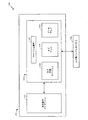
図1は、一態様による、キャッシュタグ圧縮を実現するプロセッサ101を示す。示すように、プロセッサ101は、命令を実行する命令実行パイプライン112を含む。パイプライン112は、各々が様々な非アーキテクト(non-architected)レジスタ(図示せず)と、1つまたは複数の論理演算ユニット(やはり図示せず)とを含む複数の並行パイプラインを備えたスーパースカラ設計であり得る。示すように、プロセッサ101は、1つまたは複数のより高いレベルのメモリ108からデータのラインを記憶するキャッシュ102(キャッシュメモリ102とも呼ばれる)も含む。より高いレベルのメモリ108は、限定はしないが、より高いレベルのキャッシュおよび/またはメイン(システム)メモリを含み得る。少なくとも一態様では、キャッシュ102はレベル1(L1)データキャッシュである。概して、CPU101は多数の変形形態を含むことができ、図1に示すCPU101は、例示のためであり、本開示を限定するものと見なすべきではない。たとえば、CPU101はグラフィックス処理ユニット(GPU)であり得る。
FIG. 1 illustrates a
示すように、キャッシュ102は、キャッシュ論理103と、タグ圧縮キャッシュ104と、タグアレイ105と、データアレイ106とを含む。キャッシュ論理103は、概して、キャッシュのヒットまたはミスが特定の動作において生じるかどうかの決定など、キャッシュ102の動作を制御する。タグ圧縮キャッシュ(TCC)104は、メモリタグの上位(または、高位)ビットのセットを保留するように構成されたハードウェア構造である。たとえば、TCC104は、メモリタグの上位アドレスビット、ASIDビット、セキュリティビット、例外レベルビットなどのうちの1つまたは複数を保留することができる。TCC104は、概して、場合によっては、タグアレイ105内に冗長的に記憶されることになる冗長値を記憶するように構成される。タグアレイ105は、概して、キャッシュ102内に記憶されたデータのアドレスを記憶するように構成される。より具体的には、タグアレイ105の各エントリは、TCC104内のメモリタグの低位ビットのセットおよびエントリのインデックス値に対応するインデックス値を記憶するように構成される。データアレイ106は、キャッシュラインのデータを記憶する。少なくとも一態様では、TCC104は、コンテンツアドレッサブルメモリ(CAM:content addressable memory)構造として実装される。同様に、タグアレイ105およびデータアレイ106は、CAMとして実装される。さらに、少なくとも一態様では、TCC104は、フルアソシアティブ(fully-associative)最長時間未使用(LRU:least recently used)置換構造である。TCC104は、2、4、または8など、任意の数のエントリを有し得る。TCC104、タグアレイ105、およびデータアレイ106内にデータを記憶するための手段は、1つまたは複数のメモリセルを含み得る。
As shown,
動作において、プロセッサ101は、より高いレベルのメモリ108のうちの1つの中に位置するデータがキャッシュ102内に存在するかどうかを決定することを探索することができる。プロセッサ101が(仮想アドレスであり得る)入力メモリアドレスをキャッシュ102に提供するとき、キャッシュ論理103は、入力メモリアドレスにおけるデータがキャッシュ102内にあるかどうかを決定することができる。そうするために、キャッシュ論理103は、入力メモリアドレスの高位ビットを使用して、TCC104のCAM探索を開始することができる。TCC104内のエントリが入力メモリアドレスの高位ビットと一致する場合、TCC104はTCC104内の一致するエントリのインデックス値を返すように構成される。キャッシュ論理103は、TCC104のCAM探索と平行して、タグアレイ105のCAM探索を開始することができる。キャッシュ論理103は、入力メモリアドレスの低位ビットを使用して、タグアレイ105を探索することができる。タグアレイ105内のエントリの低位ビットが入力メモリアドレスの低位ビットと一致する場合、タグアレイ105は、一致するエントリの低位ビットおよびインデックス値を返すように構成される。キャッシュ論理103は、次いで、TCC104およびタグアレイ105によって返されたインデックス値を比較することができる。インデックス値が一致しない場合、キャッシュ論理103はキャッシュミスの指示を返すことができる。キャッシュ論理103は、タグアレイ105によって返された低位ビットを入力メモリアドレスの低位ビットと比較することもできる。低位ビットが一致し、インデックス値が一致する場合、キャッシュ論理103はキャッシュヒットの指示を返すように構成される。
In operation, the
TCC104の探索の結果がミスである場合、キャッシュ論理103は、TCC104内に入力メモリアドレスに関するエントリを作成するように構成され得る。空き(またはさもなければ、利用可能な)エントリがTCC104内に存在する場合、キャッシュ論理103は、入力メモリアドレスの高位ビットのセットを空きエントリ内に記憶することができる。TCC104内で何のエントリも利用可能でない場合、キャッシュ論理103は、TCC104内の既存のエントリをエビクトし、エビクトされたエントリのインデックス値を特定する、タグアレイ105(および、データアレイ106)内の任意の対応するエントリを無効化することができる。キャッシュ論理103は、LRUなど、TCC104に適した任意の置換ポリシーを適用し得、または、(TCC104内の各エントリに関してカウンタによって決定され得る)最も少ないキャッシュラインに関連付けられるTCC104エントリを置換する。キャッシュ論理103は、フラッシュ無効化またはライン単位の無効化によってなど、いずれかの実現可能な方法でエントリを無効化することができる。入力メモリアドレスの高位ビットを特定するエントリをTCC104に追加することに加えて、キャッシュ論理103は、入力メモリアドレスの低位ビットおよび入力メモリアドレスの高位ビットを記憶するTCC104エントリのインデックス値を特定するエントリをタグアレイ105内に作成することもできる。
If the result of the search of
少なくとも一態様では、キャッシュ論理103はクロックサイクルごとにTCC104をプローブすることができる。しかしながら、これは、大量の電力を引き出す可能性があり、クリティカルタイミングパス(critical timing path)内であり得る。TCC104内に構築されたエントリが多ければ多いほど、TCC104をプローブするために、より多くの電力および時間が必要とされ得る。したがって、いくつかの態様では、キャッシュ論理103は、サイクルの大部分においてTCC104を探索する必要を回避する論理を含み得る。たとえば、レジスタのセットは、TCC104に対する前のアクセスによって返されたビット(および、対応するTCC104エントリが有効な状態に留まるかどうか)を記憶するように構成され得る。概して、キャッシュ論理103は、TCC104内に保留される入力メモリアドレスビットに対応する入力メモリアドレスビットがTCC104に対する前のアクセス内と同じであるかどうかを決定することができる。キャッシュ論理103は、次いで、関連付けられたTCC104エントリが、最後のアクセス以来、無効化されていないかどうかを決定することができる。両方の決定が真である場合、キャッシュ論理103は、圧縮キャッシュタグがTCC104内にあるはずであり、前のサイクルのインデックスの再使用が安全であると決定し、現在のサイクル内でTCC104を探索することを不要にし得る。いずれかの決定が真でない場合、キャッシュ論理103は、前のサイクルのTCC104インデックスを再使用することができず、制御論理103はTCC104を探索しなければならない。TCC104、タグアレイ105、およびデータアレイ106を探索するための手段は、ハードウェアおよび/またはソフトウェアとして実装される論理を含む。同様に、ハードウェアおよび/またはソフトウェアとして実装される論理は、値を読み取るおよび/または書き込むための手段、ヒットおよび/またはミスの指示を返すための手段、ならびにTCC104、タグアレイ105、およびデータアレイ106から値を返すための手段として働き得る。そのような手段論理の例は、メモリコントローラ、キャッシュコントローラ、およびデータコントローラを含む。
In at least one aspect,
前に示したように、図1に示す圧縮方式は、他のPCタグ付けおよび/またはASIDタグ付けされたマイクロアーキテクチャ構造に適用され得る。たとえば、仮想アドレスは、ブロックを通して使用され得る形式{タグ圧縮インデックス値、部分仮想アドレス}に変換され得る。そうすることは、すべてのデータ経路要素が、トランスレーションルックアサイドバッファ(TLB)、分岐予測器、中断点、キャッシュなどを含めて、この短縮された形式で動作することを可能にすることになる。必要な場合、ブロック境界において、キャッシュコンテンツデバッグ機能に関してなど、必要なときはいつでも、変換されたアドレスを元のアドレスに変換することができる。同様に、タグ圧縮技法を命令アドレス、ロード/記憶アドレス、および物理的にタグ付けされた構造に独立して適用することができる。 As previously indicated, the compression scheme shown in FIG. 1 can be applied to other PC-tagged and/or ASID-tagged microarchitecture structures. For example, a virtual address can be translated into a format {tag compression index value, partial virtual address} that can be used throughout the block. Doing so will allow all datapath elements to operate in this shortened form, including translation lookaside buffers (TLBs), branch predictors, breakpoints, caches, etc. .. If necessary, at a block boundary, the translated address can be translated back to the original address whenever needed, such as for cache content debug functionality. Similarly, tag compression techniques can be applied independently to instruction addresses, load/store addresses, and physically tagged structures.
一態様では、プロセッサ101を、命令実行パイプライン112とキャッシュ102とを含む集積回路上に配設することができる。別の態様では、キャッシュ102を、プロセッサ101を含む集積回路とは別個の集積回路上に配置することができる。
In one aspect, the
図2は、一態様による、キャッシュタグ圧縮を実現するように構成されたプロセッサ101のキャッシュ論理103の一部分の論理図である。示すように、プロセッサ101は、タグ圧縮キャッシュ(TCC)104とキャッシュタグアレイ105とを含む。前に説明したように、TCC104は、複数のTCCエントリ202を記憶する、インデックス付けされたハードウェア構造である。TCCエントリ202は、メモリタグの高位アドレスビットのセットを含み得る。少なくともいくつかの態様では、TCCエントリ202は、ASID、セキュリティレベル、例外レベルなどに関するビットをさらに含み得る。示すように、キャッシュタグアレイ105は、複数のエントリを含み、エントリの各々は、タグ圧縮キャッシュ(TCC)インデックス値204とキャッシュタグ205とを有する。TCCインデックス値204は、TCC104内のエントリ202のインデックス値に対応し得る。キャッシュタグ205は、メモリタグの低位ビットを含み得る。示すように、キャッシュタグ205は、メモリタグの低位ビット、すなわち、Nビットメモリタグのビット0からMを記憶する。同様に、TCC104は、Nビットのメモリタグの高位ビット、すなわち、メモリタグのビットM+1からNを記憶する。したがって、完全なメモリタグ(ビット0からN)は、TCC104内に記憶された高位ビット(ビットM+1からN)をキャッシュタグ205の低位ビット(ビット0からM)と組み合わせることによって、作成され得る。
FIG. 2 is a logic diagram of a portion of
示すように、プロセッサ101は、メモリアドレス201において記憶されたデータを要求し得る。キャッシュ論理103は、メモリアドレス201において記憶されたデータがキャッシュ102内に位置するかどうかを決定するように構成され得る。少なくとも一態様では、メモリアドレス201は、Nビットの長さを有する仮想メモリアドレスであり得る。メモリアドレス201において記憶されたデータがキャッシュ102内にあるかどうかを決定するために、キャッシュ論理103は、TCC104とキャッシュタグアレイ105とを並行してプローブすることができる。より具体的には、示すように、キャッシュ論理103は、キャッシュタグアレイ105のCAM探索を実行することができる。キャッシュタグ205のうちの1つがメモリアドレス201のビット0からMと一致するエントリを含む場合、キャッシュタグアレイ105は、TCCインデックス値208およびキャッシュタグ209を返すことができる。さらに、示すように、スプリッタ213はメモリアドレス201を分割して、メモリアドレス201のビットM+1からNをTCC104に提供することができる。TCC104上でのCAM探索は、メモリアドレス201のビットM+1からNを使用して実行され得る。TCC104内のエントリ202がメモリアドレス201のビットM+1からNの値と一致する値を含む場合、TCC104は、TCCエントリ206およびTCCインデックス値207を返すように構成され、この場合、インデックス値207は一致するTCCエントリ206を識別する。TCCインデックス値207は、TCC104内の各エントリ202がそれぞれのTCCインデックス値207によって一意に識別されることを可能にするのに適した長さの任意の数のビットであり得る。したがって、たとえば、TCC104が4個のハードウェアエントリ(たとえば、4個のTCCエントリ202)を有する場合、各エントリに対応するTCCインデックス値207は2ビットの長さであり得る。そのような例では、キャッシュタグアレイ105内に記憶された各TCCインデックス204も2ビットの長さになる。少なくとも一態様では、TCCインデックス値207は、所与のTCCエントリ202のロケーション(または、アドレス)に基づいて暗示的に識別される。
As shown, the
示すように、比較器210は、TCC104から返されたTCCインデックス値207をキャッシュタグアレイ105によって返されたTCCインデックス値208と比較する。さらに、比較器211は、メモリアドレス201の低位ビット0:Mをキャッシュタグアレイ105から返されたキャッシュタグエントリ209内に記憶された低位ビット0:Mと比較する。示すように、AND論理212は、比較器210、211の出力に関して論理AND演算を実行するように構成される。両方の比較器210、211が一致を示す場合、AND論理212の出力はキャッシュヒットの指示を返すように構成される。別の言い方をすれば、比較器210によって比較されたインデック値が一致し、比較器211によって比較された低位ビット0:Mが一致する場合、要求されるメモリアドレス201のコンテンツはキャッシュ102内に記憶され、キャッシュ論理103はキャッシュヒットの指示を返すことができる。しかしながら、比較器210が比較されたインデックス値が一致しないことを示すか、または比較器211が低位ビット0:Mが一致しないことを示す場合、要求されるデータはキャッシュ102内になく、キャッシュ論理103はキャッシュミスの指示を返すことができる。したがって、示すように、キャッシュ論理103は、ビット0:Mおよびインデックス値の比較をもたらす。そうすることは、キャッシュ論理103が(ビット0:Nの)旧来のタグ比較よりも少ないビットを比較することを可能にし、旧来の比較よりも高速の比較をもたらす。
As shown, the
キャッシュミスの場合、キャッシュ論理103は、上記で説明したように、要求されるデータを高位メモリからフェッチし、TCC104およびキャッシュタグアレイ105をポピュレートするように構成され得る。同様に、TCC104およびキャッシュタグアレイ105の最初のCAM探索のいずれかがミスである場合、キャッシュ論理103は、上記で説明したように、要求されるデータを高位メモリからフェッチし、TCC104およびキャッシュタグアレイ105をポピュレートするように構成され得る。
In the case of a cache miss,
図3は、一態様による、タグ圧縮キャッシュ(TCC)104、キャッシュタグアレイ105、およびデータアレイ106内に記憶された例示的な値を示す概略図300である。示すように、TCC104内の各TCCエントリ202は、メモリタグの一部分を特定し、それぞれのTCCインデックス値207によって識別される。それぞれのインデックス値207は、各TCCエントリ202を一意に識別する。少なくとも一態様では、インデックス値207は、TCC104内の各エントリのロケーション(または、アドレス)によって暗示的に提供される。したがって、そのような態様では、インデックス値207は、TCC104内で明確に定義されず、インデックス値207は、そのような態様の説明を容易にするために、図3に示される。各TCCエントリ202のタグ部分は、メモリタグの高位アドレスビットであり得、ASIDビット、セキュリティビット、例外レベルビットなど、追加の情報を含み得る。
FIG. 3 is a schematic diagram 300 illustrating exemplary values stored in a tag compression cache (TCC) 104, a
示すように、表301は、キャッシュタグアレイ105およびデータアレイ106の例示的な値を含む。データアレイ106は、キャッシュ102内の各エントリに関するデータライン302を記憶する。キャッシュタグアレイ105は、前に説明したように、インデックス値204とキャッシュタグ205とを含む。キャッシュタグアレイ105内のインデックス値204は、TCC104内の所与のTCCエントリ202に対応するインデックス値207に対応し、各対応するキャッシュタグ205はメモリタグの低位ビットを記憶する。したがって、示すように、表301内の複数のエントリは同じインデックス値204を記憶することができる。有利には、TCC104は、メモリタグの高位ビットのフルビットパターンの単一のコピーを記憶して、キャッシュタグアレイ105内に記憶された冗長情報の量(すなわち、異なるインデックス値204であって、メモリタグのより長い高位ビットではない)を低減させる。したがって、メモリタグは、高位ビットがTCC104内に記憶され、低位ビットがキャッシュタグアレイ105内に記憶された状態で、TCC104およびキャッシュタグアレイ105にわたって記憶される。概念的に言えば、TCC104内のTCCエントリ202のタグ部分は、完全なメモリタグを作成するために、キャッシュタグアレイ105のインデックス値204を置換し得る。たとえば、表301の第1の行において、インデックス204のビット「00」は、TCC104内の「00」のインデックス値207に対応するTCCエントリ202のタグビット「01…0100」によって置換されることになる。
As shown, table 301 includes exemplary values for
例示的な一態様では、図3に示す構成は、仮定的命令キャッシュをTable I(表1)内に示す例示的な構成で置換することができる。 In one exemplary aspect, the configuration shown in FIG. 3 can replace the hypothetical instruction cache with the exemplary configuration shown in Table I (Table 1).

したがって、Table I(表1)に示すように、仮定的命令キャッシュは、32KB(または、32,768バイト、もしくは262,144ビット)の総キャッシュストレージのうち、26,624ビットのストレージオーバーヘッドをタグストレージに対して必要とする。この例示的な構成において必要とされる命令キャッシュタグは、{PC[48:13], ASID}になる。 Therefore, as shown in Table I, the hypothetical instruction cache requires 26,624 bits of storage overhead for tag storage out of 32KB (or 32,768 bytes, or 262,144 bits) of total cache storage. To do. The instruction cache tag needed in this exemplary configuration would be {PC[48:13], ASID}.
しかしながら、これらのビットのサブセット({PC[48:28], ASID}など)は、現実世界の作業負荷において若干の変動を示す傾向がある。この例示的な命令キャッシュの場合、4個のエントリTCC104を作成することによって、各TCCエントリ202は、21 PC[48:28]ビットおよびASIDの16ビットの総計37ビットを記憶することになる。TCC104に対して必要とされる総記憶量は、したがって、4エントリ×37ビット、すなわち、148ビットになる。TCCエントリ202は、TCC104内の各それぞれのTCCエントリ202のロケーション(または、アドレス)によって暗示的にインデックス付けされ得る(たとえば、4エントリTCC104において、ロケーション0、1、2、および3は、それぞれ、00、01、10、および11のバイナリインデックス値に対応する)。一方、キャッシュタグアレイ105のインデックス204は、2ビットインデックス値を記憶することになり、キャッシュタグ205は、タグビットPC[27:13]、または15ビットの総計17ビットを記憶することになる。命令キャッシュの512本のラインにわたって、キャッシュタグアレイ105内の総記憶域は、512個のエントリ×17ビットの総計8,704ビットになる。TCC104およびキャッシュタグアレイ105にわたって必要とされる総記憶域は、8,852ビット(148+8,704)になり、これは、Table I(表1)で説明する命令キャッシュによって必要とされる26,624ビットよりもかなり少ない。
However, a subset of these bits ({PC[48:28], ASID}, etc.) tends to exhibit some variation in real-world workloads. For this exemplary instruction cache, by creating four
図4は、一態様による、キャッシュタグ圧縮を実現するための方法400を示すフローチャートである。方法400はステップ410で開始し、ここで、キャッシュ論理103は長さがNビットのメモリアドレスを受信することができる。メモリアドレスは、メモリアドレスにおいて記憶されたデータがキャッシュ102内に位置するかどうかを決定するための要求の一部として受信され得る。キャッシュ論理103は、次いで、TCC104とキャッシュタグアレイ105とを並行してプローブすることができる。より具体的には、ステップ415において、キャッシュ論理103は、ステップ410で受信されたメモリアドレスの下位Mビットを使用して、キャッシュタグアレイ105上でCAM探索を実行することができる。キャッシュタグアレイ105内のエントリがメモリアドレスの下位Mビットと一致する値を記憶している場合、キャッシュタグアレイ105内にヒットが存在し、方法はステップ460に進む。加えて、キャッシュタグアレイ105は、メモリアドレスの下位Mビットおよび一致するエントリ内に記憶されたインデックス値を返すことができる。メモリアドレスの下位Mビットと一致する値を記憶するキャッシュタグアレイ105内に何のエントリも存在しない場合、キャッシュタグアレイ105内にミスが存在し、方法はステップ480に進む。
FIG. 4 is a flowchart illustrating a
ステップ420で、キャッシュ論理103は、要求されるメモリアドレスの高位ビット(M+1からN)を使用して、TCC104をプローブすることができる。TCC104内のエントリが要求されるメモリアドレスの高位ビットと一致する値を記憶する場合、方法はステップ460に進む。TCC104内のヒットの場合、TCC104は、メモリアドレスの高位ビットと一致する、TCC104内のエントリのインデックス値を返すことができる。TCC104内にミスが存在する場合、方法はステップ430に進み、ここで、キャッシュ論理103は、TCC104内に利用可能なエントリが存在するかどうかを決定することができる。エントリが利用可能でない場合、方法はステップ440に進み、ここで、キャッシュ論理103は、TCC104内のエントリをエビクトし、キャッシュタグアレイ105内の任意の対応するエントリを無効化することができる。キャッシュ論理103は、最長時間未使用のエントリをエビクトすること、またはキャッシュタグアレイ105内の最小エントリに関連付けられた、TCC104内のエントリをエビクトすることなど、何らかの適切なエビクションポリシーを使用することができる。キャッシュ論理103は、フラッシュ無効化またはライン単位の無効化など、何らかの実現可能な方法でキャッシュタグアレイ105内のエントリを無効化することができる。図5を参照してより詳細に説明するステップ450において、キャッシュ論理103はTCC104内に新しいエントリを確立することができる。概して、キャッシュ論理103は、メモリアドレスをビット0:Mの下位セットとビットM+1:Nの高位セットに分割することができる。キャッシュ論理103は、次いで、ビットの下位セットをキャッシュタグアレイ105内に記憶し、ビットの高位セットをTCC104内に記憶することができる。
At
ステップ460で、キャッシュ論理103は、TCC104およびキャッシュタグアレイ105によって返されたインデックス値を比較することができる。キャッシュ論理103は、キャッシュタグアレイ105によって返された低位ビットを要求されるメモリアドレスの低位ビットとさらに比較することができる。両方の比較が一致をもたらす場合、この方法はステップ470に進み、ここで、キャッシュ論理はキャッシュヒットの指示を返すことができる。ステップ460において実行された比較のうちの1つ(または、両方)が一致をもたらさない場合、この方法はステップ480に進み、ここで、キャッシュ論理103はキャッシュミスの指示を返す。
At
図5は、一態様による、タグ圧縮キャッシュ104内に新しいエントリを確立するためのステップ450に対応する方法500を示すフローチャートである。示すように、方法500はステップ510で開始し、ここで、プロセッサ101は、ステップ410で提供されたメモリアドレスに関連付けられるデータをより高いレベルのメモリ(より高いレベルのキャッシュまたはメインメモリなど)から取り出すことができる。ステップ520で、キャッシュ論理103は、メモリアドレスの高位ビット(ビットM+1:Nなど)をTCC104の第1のエントリ内に記憶することができる。ステップ530で、キャッシュ論理103は、TCC104の第1のエントリのインデックス値およびメモリアドレスの低位ビット(ビット0:Mなど)をタグアレイ105の第1のエントリ内に記憶することができる。ステップ540で、キャッシュ論理103は、ステップ510で取り出されたデータをタグアレイ105の第1のエントリに対応するデータアレイ106内に記憶する。
FIG. 5 is a flowchart illustrating a method 500 corresponding to step 450 for establishing a new entry in the
図6は、一態様による、キャッシュタグ圧縮を実現するように構成されたプロセッサ101を組み込んだコンピューティングデバイス601を示すブロック図である。図1〜図5に示した装置および方法のすべては、コンピューティングデバイス601内に含まれ得るか、またはコンピューティングデバイス601によって実行され得る。コンピューティングデバイス601は、ネットワーク630を介して他のコンピューティングデバイスに接続されてもよい。概して、ネットワーク630は、電気通信ネットワークおよび/またはワイドエリアネットワーク(WAN)であり得る。特定の態様では、ネットワーク630はインターネットである。概して、コンピューティングデバイス601は、限定はしないが、デスクトップコンピュータ、ラップトップコンピュータ、タブレットコンピュータ、およびスマートフォンを含む、キャッシュタグ圧縮を実装するように構成されたプロセッサを含む任意のデバイスであってよい。
FIG. 6 is a block diagram illustrating a
コンピューティングデバイス601は、概して、バス620を介して、メモリ608、ネットワークインターフェースデバイス618、ストレージ609、入力デバイス622、および出力デバイス624に接続されたプロセッサ101を含む。コンピューティングデバイス601は、概して、オペレーティングシステム(図示せず)の制御下にある。本明細書で説明する機能をサポートする任意のオペレーティングシステムが使用され得る。プロセッサ101は、単一のCPU、複数のCPU、複数の処理コアを有する単一のCPUなどを表すように含まれる。ネットワークインターフェースデバイス618は、コンピューティングデバイス601がネットワーク630を介して他のコンピューティングデバイスと通信することを可能にする任意のタイプのネットワーク通信デバイスであり得る。
ストレージ609は、永続ストレージデバイスであってよい。ストレージ609は単一のユニットとして示されるが、ストレージ609は、固定ディスクドライブ、固体ドライブ、SANストレージ、NASストレージ、取外し可能メモリカード、または光ストレージなど、固定および/または取外し可能ストレージデバイスの組合せであり得る。メモリ608およびストレージ609は、複数の1次ストレージデバイスおよび2次ストレージデバイスにまたがる1つの仮想アドレス空間の一部であり得る。
入力デバイス622は、コンピューティングデバイス601に入力を提供するための任意のデバイスであり得る。たとえば、キーボードおよび/またはマウスを使用することができる。出力デバイス624は、コンピューティングデバイス601のユーザに出力を提供するための任意のデバイスであり得る。たとえば、出力デバイス624は、任意の従来のディスプレイスクリーンまたはスピーカのセットであってよい。入力デバイス622とは別に示されているが、出力デバイス624および入力デバイス622は結合されてよい。たとえば、一体化タッチスクリーンを備えたディスプレイスクリーンが使用され得る。
有利には、本明細書で開示する態様は、メモリタグ値を記憶するために必要とされる空間の量を低減させる。メモリタグの高位ビットの冗長値をより小さなタグ圧縮キャッシュ内に記憶することによって、より小さなタグアレイ構造を使用して、メモリタグの低位ビットを記憶することができる。そうすることは、より小さな全体的なシリコンダイを使用してそのような構造が作成されることを可能にし得、これは、他のハードウェア構造がより近くに一緒に配置されることを可能にすることによって、製造コストを削減し、漏れ電流を低減し、回路タイミングを改善する。加えて、または代替として、節約された空間を他のマイクロアーキテクチャ構造上で使うことができる。 Advantageously, the aspects disclosed herein reduce the amount of space required to store memory tag values. By storing the redundant value of the high order bits of the memory tag in a smaller tag compression cache, a smaller tag array structure can be used to store the low order bits of the memory tag. Doing so may allow such structures to be created using a smaller overall silicon die, which allows other hardware structures to be placed closer together. This reduces manufacturing costs, reduces leakage current, and improves circuit timing. Additionally or alternatively, the saved space can be used on other microarchitecture structures.
いくつかの態様が説明されてきた。しかしながら、これらの構成に対する様々な変更が可能であり、本明細書で提示した原理は他の構成にも同様に適用され得る。そのような方法の様々なタスクは、マイクロプロセッサ、埋込み型コントローラ、またはIPコアなど、論理要素の1つまたは複数のアレイによって実行可能な命令のセットとして実装され得る。 Several aspects have been described. However, various modifications to these configurations are possible and the principles presented herein may be applied to other configurations as well. The various tasks of such methods may be implemented as a set of instructions executable by one or more arrays of logic elements, such as microprocessors, embedded controllers, or IP cores.
上記で説明した方法の様々な動作は、プロセッサ、ファームウェア、特定用途向け集積回路(ASIC)、ゲート論理/レジスタ、メモリコントローラ、またはキャッシュコントローラなど、動作を実行することが可能な任意の適切な手段によって実行され得る。概して、図に示された任意の動作は、その動作を実行することが可能な対応する機能的手段によって実行され得る。 The various operations of the methods described above may be performed by any suitable means capable of performing the operations, such as a processor, firmware, application specific integrated circuit (ASIC), gate logic/register, memory controller, or cache controller. Can be performed by. In general, any act shown in the figures may be performed by corresponding functional means capable of performing the action.
上記で開示したデバイスおよび機能は、コンピュータ可読媒体上に記憶されたコンピュータファイル(たとえば、RTL、GDSII、GERBERなど)に設計および構成されてもよい。いくつかまたはすべてのそのようなファイルは、そのようなファイルに基づいてデバイスを製造する製造者に提供されてもよい。結果として得られる製品は、半導体ウエハを含み、次いで、半導体ウエハは半導体ダイに切断され、半導体チップにパッケージングされる。いくつかのまたはすべてのそのようなファイルは、本明細書で説明したデバイスを作製するために設計データを使用して作製機器を構成する製造者に提供されてよい。コンピュータファイルから形成された結果得られた製品は半導体ウエハを含み、半導体ウエハは、次いで、半導体ダイ(たとえば、プロセッサ101)に切断され、パッケージングされ、限定はしないが、モバイルフォン、スマートフォン、ラップトップ、ネットブック、タブレット、ウルトラブック、デスクトップコンピュータ、デジタルビデオレコーダ、セットトップボックス、および集積回路が使用される任意の他のデバイスを含む製品にさらに組み込まれ得る。 The devices and functions disclosed above may be designed and configured into computer files (eg, RTL, GDSII, GERBER, etc.) stored on a computer-readable medium. Some or all such files may be provided to a manufacturer who manufactures devices based on such files. The resulting product comprises a semiconductor wafer, which is then cut into semiconductor dies and packaged in semiconductor chips. Some or all such files may be provided to the manufacturer who configures the fabrication equipment using the design data to fabricate the devices described herein. The resulting products formed from the computer files include semiconductor wafers, which are then cut into semiconductor dies (e.g., processor 101) and packaged, including but not limited to mobile phones, smartphones, and wraps. It can be further incorporated into products including tops, netbooks, tablets, ultrabooks, desktop computers, digital video recorders, set-top boxes, and any other device in which integrated circuits are used.
一態様では、コンピュータファイルは、上記で説明し、物理的な設計レイアウト、概略図、ハードウェア記述言語(たとえば、Verilog、VHDLなど)の形態で、図で示した回路を含む設計構造を形成する。たとえば、設計構造は、テキストファイルまたは上記で説明し、図に示したような回路のグラフィカル表現であってよい。設計プロセスは、好ましくは、下記で説明する回路をネットリストに合成し(たとえば、変換し)、この場合、ネットリストは、たとえば、集積回路設計内の他の要素および回路に対する接続を記述し、機械可読媒体のうちの少なくとも1つの上に記録される、ワイヤ、トランジスタ、論理ゲート、制御回路、I/O、モデルなどのリストである。たとえば、媒体は、CD、コンパクトフラッシュ(登録商標)、他のフラッシュメモリ、またはハードディスクドライブなどの記憶媒体であり得る。別の態様では、本明細書で説明したハードウェア、回路、および方法は、プロセッサによって実行されると、上記で説明し、図に示した回路の機能をシミュレートするコンピュータファイルに構成され得る。これらのコンピュータファイルは、回路シミュレーションツール、回路図エディタ、または他のソフトウェアアプリケーション内で使用され得る。 In one aspect, the computer files form the design structure described above and in the form of a physical design layout, schematic, hardware description language (eg, Verilog, VHDL, etc.) that includes the circuits shown. .. For example, the design structure may be a text file or a graphical representation of the circuit as described above and shown in the figures. The design process preferably synthesizes (e.g., transforms) the circuits described below into a netlist, where the netlist describes, for example, connections to other elements and circuits in the integrated circuit design, A list of wires, transistors, logic gates, control circuits, I/Os, models, etc. recorded on at least one of the machine-readable media. For example, the medium may be a storage medium such as a CD, CompactFlash®, other flash memory, or hard disk drive. In another aspect, the hardware, circuits, and methods described herein can be configured into computer files that, when executed by a processor, simulate the functionality of the circuits described above and illustrated in the figures. These computer files may be used within circuit simulation tools, schematic editors, or other software applications.
本明細書で開示した態様の実装形態は、(たとえば、本明細書に記載する1つまたは複数のコンピュータ可読記憶媒体の有形なコンピュータ可読特徴中で)論理要素のアレイ(たとえば、プロセッサ、マイクロプロセッサ、マイクロコントローラ、または他の有限状態機械)を含む機械によって実行可能な命令の1つまたは複数のセットとしても有形に実施され得る。「コンピュータ可読媒体」という用語は、情報を記憶または転送することができる、揮発性、不揮発性、取外し可能および取外し不可能な記憶媒体を含む、任意の媒体を含み得る。コンピュータ可読媒体の例は、電子回路、半導体メモリデバイス、ROM、フラッシュメモリ、消去可能ROM(EROM)、フロッピーディスケットもしくは他の磁気ストレージ、CD-ROM/DVDもしくは他の光ストレージ、ハードディスクもしくは所望の情報を記憶するのに使われ得る任意の他の媒体、光ファイバー媒体、無線周波(RF)リンク、または所望の情報を運ぶために使用され得るとともにアクセスされ得る任意の他の媒体を含む。コンピュータデータ信号は、電子ネットワークチャネル、光ファイバー、無線リンク、電磁リンク、RFリンクなどの伝送媒体を介して伝播することができる、任意の信号を含み得る。コードセグメントは、インターネットまたはイントラネットなどのコンピュータネットワークを介してダウンロードされ得る。いずれの場合も、本開示の範囲は、そのような態様によって限定されると解釈すべきではない。 Implementations of aspects disclosed herein may include an array of logical elements (e.g., in a tangible computer readable feature of one or more computer readable storage media described herein) (e.g., processor, microprocessor). , Microcontrollers, or other finite state machines), and may also be tangibly implemented as one or more sets of instructions executable by a machine. The term "computer-readable medium" may include any medium that can store or transfer information, including volatile, nonvolatile, removable and non-removable storage media. Examples of computer readable media are electronic circuits, semiconductor memory devices, ROM, flash memory, erasable ROM (EROM), floppy diskette or other magnetic storage, CD-ROM/DVD or other optical storage, hard disk or desired information. Media, fiber optic media, radio frequency (RF) links, or any other media that can be used to carry desired information and that can be accessed. Computer data signals can include any signal that can propagate via a transmission medium such as electronic network channels, optical fibers, wireless links, electromagnetic links, RF links, and the like. Code segments may be downloaded via a computer network such as the internet or an intranet. In any case, the scope of the present disclosure should not be construed as limited by such aspects.
開示した態様の上記の説明は、開示した態様を当業者が作成または使用できるようにするために提供される。これらの態様への様々な修正は当業者には容易に明らかになり、本明細書で定義された原理は、本開示の範囲から逸脱することなく、他の態様に適用されてもよい。したがって、本開示は、本明細書に示す態様に限定されることを意図するものではなく、以下の特許請求の範囲によって定義される原理および新規な特徴と可能な限り一致する最も広い範囲が与えられるべきである。 The above description of the disclosed aspects is provided to enable any person skilled in the art to make or use the disclosed aspects. Various modifications to these aspects will be readily apparent to those skilled in the art, and the principles defined herein may be applied to other aspects without departing from the scope of this disclosure. Therefore, this disclosure is not intended to be limited to the embodiments set forth herein, but given the broadest possible scope consistent with the principles and novel features defined by the following claims. Should be done.
101 プロセッサ、CPU
102 キャッシュ、キャッシュメモリ
103 キャッシュ論理
104 タグ圧縮キャッシュ、TCC
105 キャッシュタグアレイ
106 データアレイ
108 メモリ
112 命令実行パイプライン、パイプライン
201 メモリアドレス
202 TCCエントリ
204 TCCインデックス値
205 キャッシュタグ
206 TCCエントリ
207 TCCインデックス値、インデックス値
208 TCCインデックス値
209 キャッシュタグ
210 比較器
211 比較器
212 AND論理
213 スプリッタ
300 概略図
400 方法
500 方法
601 コンピューティングデバイス
608 メモリ
609 ストレージ
618 ネットワークインターフェースデバイス
620 バス
622 入力デバイス
624 出力デバイス
630 ネットワーク
101 processor, CPU
102 cache, cache memory
103 cache logic
104 tag compression cache, TCC
105 cache tag array
106 data array
108 memory
112 Instruction execution pipeline, pipeline
201 memory address
202 TCC entry
204 TCC index value
205 cache tag
206 TCC entry
207 TCC index value, index value
208 TCC index value
209 cash tag
210 comparator
211 Comparator
212 AND logic
213 Splitter
300 schematic
400 ways
500 ways
601 computing device
608 memory
609 storage
618 Network Interface Device
620 bus
622 Input device
624 Output device
630 network
Claims (15)
複数のタグ圧縮エントリを記憶するタグ圧縮構造であって、前記複数のタグ圧縮エントリのうちの少なくとも1つが、少なくとも2つのメモリタグによって共有される所定の長さの高位ビットの一意のセットを含み、それぞれのインデックス値によって識別される、タグ圧縮構造と、
複数のタグアレイエントリを記憶するタグアレイであって、前記複数のタグアレイエントリの各々が、前記メモリタグのうちの1つの所定の長さの低位ビットのそれぞれのセットと、インデックス値とを含み、各タグアレイエントリの前記インデックス値が、それぞれの前記タグアレイエントリの前記メモリタグの前記高位ビットを含む前記タグ圧縮構造エントリの前記インデックス値に対応し、前記複数のメモリタグの各々が、データアレイ内に記憶されたデータ要素のそれぞれのメモリアドレスの少なくとも一部分を備える、タグアレイと
を備える、キャッシュメモリ。 Cache memory,
A tag compression structure storing a plurality of tag compression entries, wherein at least one of the plurality of tag compression entries comprises a unique set of high order bits of a predetermined length shared by at least two memory tags. , A tag compression structure, identified by respective index values,
A tag array storing a plurality of tag array entries, each of the plurality of tag array entries including a respective set of low order bits of a predetermined length of one of the memory tags, and an index value, The index value of each tag array entry corresponds to the index value of the tag compression structure entry including the high-order bit of the memory tag of each tag array entry, and each of the plurality of memory tags includes a data array. A tag array comprising at least a portion of a memory address of each of the data elements stored therein.
前記入力メモリアドレスの低位ビットの前記セットが第1のタグアレイエントリ内の前記メモリタグの低位ビットの前記セットと一致するとの決定時に、前記第1のタグアレイエントリ内に記憶された前記インデックス値および前記メモリタグの低位ビットの前記セットを返すことと、
前記第1のタグ圧縮エントリの前記返されたインデックス値が前記第1のタグアレイエントリの前記返されたインデックス値と一致すると決定することと
によって、前記入力メモリアドレスに関する前記タグアレイ内のヒットの指示を返すように構成された論理をさらに備える、請求項1に記載のキャッシュメモリ。 The index corresponding to the first tag compression entry from the tag compression structure upon determining that the set of high bits of the memory tag in the first tag compression entry matches a set of high bits of an input memory address. Returning a value,
The index value stored in the first tag array entry upon determining that the low bit of the input memory address matches the low bit of the memory tag in the first tag array entry. And returning the set of low order bits of the memory tag;
An indication of a hit in the tag array for the input memory address by determining that the returned index value of the first tag compression entry matches the returned index value of the first tag array entry. The cache memory of claim 1, further comprising logic configured to return.
前記入力メモリアドレスの低位ビットのセットが、前記複数のタグアレイエントリ内に記憶された低位ビットの前記セットのうちのいずれにも一致しないこと、
前記入力メモリアドレスの前記低位ビットと一致する低位ビットのセットを記憶するタグアレイエントリから返されたインデックス値が前記入力メモリアドレスの前記高位ビットと一致する高位ビットのセットを記憶するタグ圧縮エントリのインデックス値と一致しないこと
のうちの少なくとも1つの決定時に、前記入力メモリアドレスに関する前記タグアレイ内のミスの指示を返すように構成された論理をさらに備える、請求項1に記載のキャッシュメモリ。 The set of high order bits of the input memory address does not match any of the set of high order bits in the plurality of tag compression entries,
The set of low-order bits of the input memory address does not match any of the sets of low-order bits stored in the plurality of tag array entries,
Of a tag compression entry storing a set of high-order bits whose index value returned from a tag array entry storing a set of low-order bits matching the low-order bit of the input memory address matches the high-order bit of the input memory address The cache memory of claim 1, further comprising logic configured to return an indication of a miss in the tag array for the input memory address upon determining at least one of a mismatch with an index value.
メモリ階層の次のレベルにおいて記憶されたデータを取り出すことと、
前記データを前記データアレイの第1のエントリ内に記憶することと、
前記入力メモリアドレスの高位ビットのセットを前記タグ圧縮構造内の第2のタグ圧縮エントリ内に記憶することと、
(i)前記入力メモリアドレスの低位ビットのセット、および(ii)前記第2のタグ圧縮エントリに対応するインデックス値を前記タグアレイの第2のタグアレイエントリ内に記憶することであって、前記第2のタグアレイエントリが前記データアレイの前記第1のエントリに対応する、記憶することと
を行うように構成された論理をさらに備える、請求項3に記載のキャッシュメモリ。 In response to returning the indication of the miss in the tag array,
Retrieving the data stored at the next level of the memory hierarchy,
Storing the data in a first entry of the data array;
Storing a set of high order bits of the input memory address in a second tag compression entry in the tag compression structure;
storing (i) a set of low order bits of the input memory address, and (ii) an index value corresponding to the second tag compression entry in a second tag array entry of the tag array, The cache memory of claim 3, further comprising two tag array entries corresponding to the first entry of the data array and configured to perform storage.
タグアレイ内の複数のタグアレイエントリの第1のタグアレイエントリ内に、前記第1のメモリタグの所定の長さの低位ビットのセットおよび前記第1のタグアレイエントリに関するインデックス値を記憶するステップであって、前記第1のタグアレイエントリの前記インデックス値が、前記第1のタグ圧縮エントリの前記インデックス値に対応し、前記第1のメモリタグが、データアレイ内に記憶されたデータ要素のメモリアドレスの少なくとも一部分を備え、前記複数のタグアレイエントリの第2のタグアレイエントリが、前記第1のタグ圧縮エントリに対応するインデックス値を特定し、前記第2のメモリタグの低位ビットのセットを記憶し、前記第2のメモリタグの低位ビットの前記セットが、前記第1のメモリタグの低位ビットの前記セットと一致しない、記憶するステップと
を含む、方法。 Storing in the first tag compression entry of the plurality of tag compression entries in the tag compression structure a set of high order bits of a predetermined length shared by the first memory tag and the second memory tag. Storing each of the plurality of tag compression entries, identified by a respective index value,
Storing a set of low-order bits of a predetermined length of the first memory tag and an index value for the first tag array entry in a first tag array entry of a plurality of tag array entries in a tag array. Wherein the index value of the first tag array entry corresponds to the index value of the first tag compression entry, and the first memory tag is a memory of data elements stored in a data array. A second tag array entry of the plurality of tag array entries, which comprises at least a portion of an address, identifies an index value corresponding to the first tag compression entry, and sets a low-order bit set of the second memory tag. Storing, said storing the low-order bit of the second memory tag does not match the low-order bit of the first memory tag.
前記入力メモリアドレスの低位ビットの前記セットが前記第1のタグアレイエントリ内の前記メモリタグの低位ビットの前記セットと一致するとの決定時に、前記第1のタグアレイエントリ内に記憶された前記インデックス値および前記メモリタグの低位ビットの前記セットを返すことと、
前記第1のタグ圧縮エントリの前記返されたインデックス値が前記第1のタグアレイエントリの前記返されたインデックス値と一致すると決定することと
によって、前記入力メモリアドレスに関する前記タグアレイ内のヒットの指示を返すステップをさらに含む、請求項9に記載の方法。 The tag compression structure corresponding to the first tag compression entry from the tag compression structure upon determining that the set of high bits of the memory tag in the first tag compression entry matches a set of high bits of an input memory address. Returning an index value,
The index stored in the first tag array entry upon determination that the set of low-order bits of the input memory address matches the set of low-order bits of the memory tag in the first tag array entry. Returning a value and the set of low order bits of the memory tag;
An indication of a hit in the tag array for the input memory address by determining that the returned index value of the first tag compression entry matches the returned index value of the first tag array entry. 10. The method of claim 9, further comprising returning.
入力メモリアドレスの高位ビットのセットが、前記複数のタグ圧縮エントリ内の高位ビットの前記セットのうちのいずれにも一致しないこと、
前記入力メモリアドレスの低位ビットのセットが、前記複数のタグアレイエントリ内に記憶された低位ビットの前記セットのうちのいずれにも一致しないこと、
前記入力メモリアドレスの前記低位ビットと一致する低位ビットのセットを記憶するタグアレイエントリから返されたインデックス値が前記入力メモリアドレスの前記高位ビットと一致する高位ビットのセットを記憶するタグ圧縮エントリのインデックス値と一致しないこと
のうちの少なくとも1つの決定時に、前記入力メモリアドレスに関する前記タグアレイ内のミスの指示を返すステップをさらに含む、請求項9に記載の方法。 Each of the plurality of tag compression entries in the tag compression structure is configured to store a unique set of high order bits of a predetermined length shared by a respective plurality of memory tags, and the plurality of tag arrays. Each of the entries is configured to store a set of low order bits of a predetermined length of a respective memory tag and an index value, the index value of each tag array entry being the memory tag of the respective tag array entry. Corresponding to the index value of the tag compression entry containing the high-order bit of
The set of high order bits of the input memory address does not match any of the set of high order bits in the plurality of tag compression entries,
The set of low-order bits of the input memory address does not match any of the sets of low-order bits stored in the plurality of tag array entries,
Of a tag compression entry storing a set of high-order bits whose index value returned from a tag array entry storing a set of low-order bits matching the low-order bit of the input memory address matches the high-order bit of the input memory address 10. The method of claim 9, further comprising returning a miss indication in the tag array for the input memory address upon determination of at least one of a mismatch with an index value.
メモリ階層の次のレベルにおいて記憶されたデータを取り出すステップと、
前記データを前記データアレイの第1のエントリ内に記憶するステップと、
前記入力メモリアドレスの高位ビットのセットを前記タグ圧縮構造内の第2のタグ圧縮エントリ内に記憶するステップと、
(i)前記入力メモリアドレスの低位ビットのセット、および(ii)前記第2のタグ圧縮エントリに対応するインデックス値を前記タグアレイの第2のタグアレイエントリ内に記憶するステップであって、前記第2のタグアレイエントリが前記データアレイの前記第1のエントリに対応する、記憶するステップと
をさらに含む、請求項11に記載の方法。 In response to returning the indication of the miss in the tag array,
Retrieving the data stored at the next level of the memory hierarchy,
Storing the data in a first entry of the data array,
Storing a set of high order bits of the input memory address in a second tag compression entry in the tag compression structure;
storing (i) a set of low-order bits of the input memory address, and (ii) an index value corresponding to the second tag compression entry in a second tag array entry of the tag array, Storing two tag array entries corresponding to the first entry of the data array.
タグ圧縮構造内の複数のタグ圧縮エントリの第1のタグ圧縮エントリ内に、第1のメモリタグおよび第2のメモリタグによって共有される所定の長さの高位ビットのセットを記憶することであって、前記複数のタグ圧縮エントリの各々が、それぞれのインデックス値によって識別される、記憶することと、
タグアレイ内の複数のタグアレイエントリの第1のタグアレイエントリ内に、前記第1のメモリタグの所定の長さの低位ビットのセットおよび前記第1のタグアレイエントリに関するインデックス値を記憶することであって、前記第1のタグアレイエントリの前記インデックス値が、前記第1のタグ圧縮エントリの前記インデックス値に対応し、前記第1のメモリタグが、データアレイ内に記憶されたデータ要素のメモリアドレスの少なくとも一部分を備え、前記複数のタグアレイエントリの第2のタグアレイエントリが、前記第1のタグ圧縮エントリに対応するインデックス値を特定し、前記第2のメモリタグの低位ビットのセットを記憶し、前記第2のメモリタグの低位ビットの前記セットが、前記第1のメモリタグの低位ビットの前記セットと一致しない、記憶することと
を含む、コンピュータ可読記憶媒体。 A computer readable storage medium having stored thereon instructions that, when executed by a processor, cause the processor to perform an operation, the operation comprising:
Storing a set of high order bits of a predetermined length shared by a first memory tag and a second memory tag within a first tag compression entry of a plurality of tag compression entries within a tag compression structure. Storing each of the plurality of tag compression entries, identified by a respective index value,
Storing a set of low-order bits of a predetermined length of the first memory tag and an index value for the first tag array entry in a first tag array entry of a plurality of tag array entries in the tag array. Wherein the index value of the first tag array entry corresponds to the index value of the first tag compression entry, and the first memory tag is a memory of data elements stored in a data array. A second tag array entry of the plurality of tag array entries, which comprises at least a portion of an address, identifies an index value corresponding to the first tag compression entry, and sets a low-order bit set of the second memory tag. Storing and storing the set of low-order bits of the second memory tag does not match the set of low-order bits of the first memory tag.
Applications Claiming Priority (3)
| Application Number | Priority Date | Filing Date | Title |
|---|---|---|---|
| US14/716,947 US9514061B1 (en) | 2015-05-20 | 2015-05-20 | Method and apparatus for cache tag compression |
| US14/716,947 | 2015-05-20 | ||
| PCT/US2016/026664 WO2016186747A1 (en) | 2015-05-20 | 2016-04-08 | Method and apparatus for cache tag compression |
Publications (3)
| Publication Number | Publication Date |
|---|---|
| JP2018519570A JP2018519570A (en) | 2018-07-19 |
| JP2018519570A5 JP2018519570A5 (en) | 2019-04-25 |
| JP6724043B2 true JP6724043B2 (en) | 2020-07-15 |
Family
ID=55755783
Family Applications (1)
| Application Number | Title | Priority Date | Filing Date |
|---|---|---|---|
| JP2017559370A Active JP6724043B2 (en) | 2015-05-20 | 2016-04-08 | Method and apparatus for cache tag compression |
Country Status (10)
| Country | Link |
|---|---|
| US (1) | US9514061B1 (en) |
| EP (1) | EP3298493B1 (en) |
| JP (1) | JP6724043B2 (en) |
| KR (1) | KR102138697B1 (en) |
| CN (1) | CN107735773B (en) |
| AU (1) | AU2016265131B2 (en) |
| ES (1) | ES2787002T3 (en) |
| HU (1) | HUE049200T2 (en) |
| TW (1) | TWI698745B (en) |
| WO (1) | WO2016186747A1 (en) |
Families Citing this family (10)
| Publication number | Priority date | Publication date | Assignee | Title |
|---|---|---|---|---|
| US9996471B2 (en) * | 2016-06-28 | 2018-06-12 | Arm Limited | Cache with compressed data and tag |
| US10387305B2 (en) * | 2016-12-23 | 2019-08-20 | Intel Corporation | Techniques for compression memory coloring |
| US10061698B2 (en) * | 2017-01-31 | 2018-08-28 | Qualcomm Incorporated | Reducing or avoiding buffering of evicted cache data from an uncompressed cache memory in a compression memory system when stalled write operations occur |
| US10254961B2 (en) | 2017-02-21 | 2019-04-09 | International Business Machines Corporation | Dynamic load based memory tag management |
| US10229061B2 (en) * | 2017-07-14 | 2019-03-12 | International Business Machines Corporation | Method and arrangement for saving cache power |
| US10831669B2 (en) | 2018-12-03 | 2020-11-10 | International Business Machines Corporation | Systems, methods and computer program products using multi-tag storage for efficient data compression in caches |
| US11720495B2 (en) * | 2019-05-24 | 2023-08-08 | Texas Instmments Incorporated | Multi-level cache security |
| US10983915B2 (en) * | 2019-08-19 | 2021-04-20 | Advanced Micro Devices, Inc. | Flexible dictionary sharing for compressed caches |
| US11436144B2 (en) * | 2020-04-10 | 2022-09-06 | Micron Technology, Inc. | Cache memory addressing |
| KR20230158257A (en) * | 2022-05-11 | 2023-11-20 | 서울시립대학교 산학협력단 | Method for processing instruction and processor therefor |
Family Cites Families (14)
| Publication number | Priority date | Publication date | Assignee | Title |
|---|---|---|---|---|
| GB9226660D0 (en) * | 1992-12-22 | 1993-02-17 | Assersohn Roy J B | Database system |
| US6122709A (en) * | 1997-12-19 | 2000-09-19 | Sun Microsystems, Inc. | Cache with reduced tag information storage |
| US6795897B2 (en) | 2002-05-15 | 2004-09-21 | International Business Machines Corporation | Selective memory controller access path for directory caching |
| US7162669B2 (en) | 2003-06-10 | 2007-01-09 | Hewlett-Packard Development Company, L.P. | Apparatus and method for compressing redundancy information for embedded memories, including cache memories, of integrated circuits |
| US7512750B2 (en) | 2003-12-31 | 2009-03-31 | Intel Corporation | Processor and memory controller capable of use in computing system that employs compressed cache lines' worth of information |
| US7277988B2 (en) * | 2004-10-29 | 2007-10-02 | International Business Machines Corporation | System, method and storage medium for providing data caching and data compression in a memory subsystem |
| US8806101B2 (en) * | 2008-12-30 | 2014-08-12 | Intel Corporation | Metaphysical address space for holding lossy metadata in hardware |
| US8627041B2 (en) | 2009-10-09 | 2014-01-07 | Nvidia Corporation | Efficient line and page organization for compression status bit caching |
| JP2012003314A (en) * | 2010-06-14 | 2012-01-05 | Renesas Electronics Corp | Cache memory device |
| US8838897B2 (en) * | 2011-06-29 | 2014-09-16 | New Jersey Institute Of Technology | Replicating tag entries for reliability enhancement in cache tag arrays |
| WO2013095525A1 (en) * | 2011-12-22 | 2013-06-27 | Intel Corporation | Content-aware caches for reliability |
| US9348762B2 (en) * | 2012-12-19 | 2016-05-24 | Nvidia Corporation | Technique for accessing content-addressable memory |
| US9396122B2 (en) * | 2013-04-19 | 2016-07-19 | Apple Inc. | Cache allocation scheme optimized for browsing applications |
| TWI514145B (en) * | 2013-10-21 | 2015-12-21 | Univ Nat Sun Yat Sen | Processor and cache, control method thereof for data trace storage |
-
2015
- 2015-05-20 US US14/716,947 patent/US9514061B1/en active Active
-
2016
- 2016-04-08 AU AU2016265131A patent/AU2016265131B2/en active Active
- 2016-04-08 JP JP2017559370A patent/JP6724043B2/en active Active
- 2016-04-08 KR KR1020177033433A patent/KR102138697B1/en active IP Right Grant
- 2016-04-08 WO PCT/US2016/026664 patent/WO2016186747A1/en active Application Filing
- 2016-04-08 CN CN201680026963.6A patent/CN107735773B/en active Active
- 2016-04-08 ES ES16717073T patent/ES2787002T3/en active Active
- 2016-04-08 EP EP16717073.7A patent/EP3298493B1/en active Active
- 2016-04-08 HU HUE16717073A patent/HUE049200T2/en unknown
- 2016-04-19 TW TW105112179A patent/TWI698745B/en active
Also Published As
| Publication number | Publication date |
|---|---|
| CN107735773A (en) | 2018-02-23 |
| WO2016186747A1 (en) | 2016-11-24 |
| TWI698745B (en) | 2020-07-11 |
| HUE049200T2 (en) | 2020-09-28 |
| CN107735773B (en) | 2021-02-05 |
| TW201706853A (en) | 2017-02-16 |
| KR102138697B1 (en) | 2020-07-28 |
| BR112017024623A2 (en) | 2018-07-31 |
| US20160342530A1 (en) | 2016-11-24 |
| AU2016265131B2 (en) | 2020-09-10 |
| AU2016265131A1 (en) | 2017-11-02 |
| KR20180008507A (en) | 2018-01-24 |
| US9514061B1 (en) | 2016-12-06 |
| EP3298493B1 (en) | 2020-02-12 |
| ES2787002T3 (en) | 2020-10-14 |
| EP3298493A1 (en) | 2018-03-28 |
| JP2018519570A (en) | 2018-07-19 |
Similar Documents
| Publication | Publication Date | Title |
|---|---|---|
| JP6724043B2 (en) | Method and apparatus for cache tag compression | |
| US7739477B2 (en) | Multiple page size address translation incorporating page size prediction | |
| KR102244191B1 (en) | Data processing apparatus having cache and translation lookaside buffer | |
| US9519588B2 (en) | Bounded cache searches | |
| US9311239B2 (en) | Power efficient level one data cache access with pre-validated tags | |
| KR101898322B1 (en) | Cache system with a primary cache and an overflow cache that use different indexing schemes | |
| US10303608B2 (en) | Intelligent data prefetching using address delta prediction | |
| US8327121B2 (en) | Data cache receive flop bypass | |
| JP7449694B2 (en) | Configurable skew associativity in translation index buffers | |
| US20210042120A1 (en) | Data prefetching auxiliary circuit, data prefetching method, and microprocessor | |
| US10318436B2 (en) | Precise invalidation of virtually tagged caches | |
| US20170046278A1 (en) | Method and apparatus for updating replacement policy information for a fully associative buffer cache | |
| US9507729B2 (en) | Method and processor for reducing code and latency of TLB maintenance operations in a configurable processor | |
| JP6767569B2 (en) | Methods and devices for power reduction in multithreaded mode | |
| US6460117B1 (en) | Set-associative cache memory having a mechanism for migrating a most recently used set | |
| CN113641403A (en) | Microprocessor and method implemented in microprocessor | |
| CN115964309A (en) | Prefetching | |
| BR112017024623B1 (en) | METHOD AND EQUIPMENT FOR CACHE INDICATOR COMPRESSION |
Legal Events
| Date | Code | Title | Description |
|---|---|---|---|
| A521 | Request for written amendment filed |
Free format text: JAPANESE INTERMEDIATE CODE: A523 Effective date: 20171121 |
|
| A521 | Request for written amendment filed |
Free format text: JAPANESE INTERMEDIATE CODE: A523 Effective date: 20190315 |
|
| A621 | Written request for application examination |
Free format text: JAPANESE INTERMEDIATE CODE: A621 Effective date: 20190315 |
|
| A977 | Report on retrieval |
Free format text: JAPANESE INTERMEDIATE CODE: A971007 Effective date: 20191223 |
|
| A131 | Notification of reasons for refusal |
Free format text: JAPANESE INTERMEDIATE CODE: A131 Effective date: 20200114 |
|
| A521 | Request for written amendment filed |
Free format text: JAPANESE INTERMEDIATE CODE: A523 Effective date: 20200217 |
|
| TRDD | Decision of grant or rejection written | ||
| A01 | Written decision to grant a patent or to grant a registration (utility model) |
Free format text: JAPANESE INTERMEDIATE CODE: A01 Effective date: 20200601 |
|
| A61 | First payment of annual fees (during grant procedure) |
Free format text: JAPANESE INTERMEDIATE CODE: A61 Effective date: 20200624 |
|
| R150 | Certificate of patent or registration of utility model |
Ref document number: 6724043 Country of ref document: JP Free format text: JAPANESE INTERMEDIATE CODE: R150 |
|
| R250 | Receipt of annual fees |
Free format text: JAPANESE INTERMEDIATE CODE: R250 |