JP6713934B2 - Storage device and its operating method and system - Google Patents
Storage device and its operating method and system Download PDFInfo
- Publication number
- JP6713934B2 JP6713934B2 JP2017001652A JP2017001652A JP6713934B2 JP 6713934 B2 JP6713934 B2 JP 6713934B2 JP 2017001652 A JP2017001652 A JP 2017001652A JP 2017001652 A JP2017001652 A JP 2017001652A JP 6713934 B2 JP6713934 B2 JP 6713934B2
- Authority
- JP
- Japan
- Prior art keywords
- data
- memory
- dcv
- storage device
- compressed value
- Prior art date
- Legal status (The legal status is an assumption and is not a legal conclusion. Google has not performed a legal analysis and makes no representation as to the accuracy of the status listed.)
- Active
Links
Images


Classifications
-
- G—PHYSICS
- G06—COMPUTING; CALCULATING OR COUNTING
- G06F—ELECTRIC DIGITAL DATA PROCESSING
- G06F3/00—Input arrangements for transferring data to be processed into a form capable of being handled by the computer; Output arrangements for transferring data from processing unit to output unit, e.g. interface arrangements
- G06F3/06—Digital input from, or digital output to, record carriers, e.g. RAID, emulated record carriers or networked record carriers
- G06F3/0601—Interfaces specially adapted for storage systems
- G06F3/0602—Interfaces specially adapted for storage systems specifically adapted to achieve a particular effect
- G06F3/0604—Improving or facilitating administration, e.g. storage management
-
- G—PHYSICS
- G06—COMPUTING; CALCULATING OR COUNTING
- G06F—ELECTRIC DIGITAL DATA PROCESSING
- G06F3/00—Input arrangements for transferring data to be processed into a form capable of being handled by the computer; Output arrangements for transferring data from processing unit to output unit, e.g. interface arrangements
- G06F3/06—Digital input from, or digital output to, record carriers, e.g. RAID, emulated record carriers or networked record carriers
- G06F3/0601—Interfaces specially adapted for storage systems
- G06F3/0602—Interfaces specially adapted for storage systems specifically adapted to achieve a particular effect
- G06F3/0614—Improving the reliability of storage systems
-
- G—PHYSICS
- G06—COMPUTING; CALCULATING OR COUNTING
- G06F—ELECTRIC DIGITAL DATA PROCESSING
- G06F12/00—Accessing, addressing or allocating within memory systems or architectures
- G06F12/02—Addressing or allocation; Relocation
- G06F12/0223—User address space allocation, e.g. contiguous or non contiguous base addressing
- G06F12/023—Free address space management
- G06F12/0253—Garbage collection, i.e. reclamation of unreferenced memory
-
- G—PHYSICS
- G06—COMPUTING; CALCULATING OR COUNTING
- G06F—ELECTRIC DIGITAL DATA PROCESSING
- G06F3/00—Input arrangements for transferring data to be processed into a form capable of being handled by the computer; Output arrangements for transferring data from processing unit to output unit, e.g. interface arrangements
- G06F3/06—Digital input from, or digital output to, record carriers, e.g. RAID, emulated record carriers or networked record carriers
- G06F3/0601—Interfaces specially adapted for storage systems
- G06F3/0602—Interfaces specially adapted for storage systems specifically adapted to achieve a particular effect
- G06F3/0608—Saving storage space on storage systems
-
- G—PHYSICS
- G06—COMPUTING; CALCULATING OR COUNTING
- G06F—ELECTRIC DIGITAL DATA PROCESSING
- G06F3/00—Input arrangements for transferring data to be processed into a form capable of being handled by the computer; Output arrangements for transferring data from processing unit to output unit, e.g. interface arrangements
- G06F3/06—Digital input from, or digital output to, record carriers, e.g. RAID, emulated record carriers or networked record carriers
- G06F3/0601—Interfaces specially adapted for storage systems
- G06F3/0602—Interfaces specially adapted for storage systems specifically adapted to achieve a particular effect
- G06F3/061—Improving I/O performance
- G06F3/0611—Improving I/O performance in relation to response time
-
- G—PHYSICS
- G06—COMPUTING; CALCULATING OR COUNTING
- G06F—ELECTRIC DIGITAL DATA PROCESSING
- G06F3/00—Input arrangements for transferring data to be processed into a form capable of being handled by the computer; Output arrangements for transferring data from processing unit to output unit, e.g. interface arrangements
- G06F3/06—Digital input from, or digital output to, record carriers, e.g. RAID, emulated record carriers or networked record carriers
- G06F3/0601—Interfaces specially adapted for storage systems
- G06F3/0602—Interfaces specially adapted for storage systems specifically adapted to achieve a particular effect
- G06F3/0614—Improving the reliability of storage systems
- G06F3/0616—Improving the reliability of storage systems in relation to life time, e.g. increasing Mean Time Between Failures [MTBF]
-
- G—PHYSICS
- G06—COMPUTING; CALCULATING OR COUNTING
- G06F—ELECTRIC DIGITAL DATA PROCESSING
- G06F3/00—Input arrangements for transferring data to be processed into a form capable of being handled by the computer; Output arrangements for transferring data from processing unit to output unit, e.g. interface arrangements
- G06F3/06—Digital input from, or digital output to, record carriers, e.g. RAID, emulated record carriers or networked record carriers
- G06F3/0601—Interfaces specially adapted for storage systems
- G06F3/0628—Interfaces specially adapted for storage systems making use of a particular technique
- G06F3/0629—Configuration or reconfiguration of storage systems
- G06F3/0635—Configuration or reconfiguration of storage systems by changing the path, e.g. traffic rerouting, path reconfiguration
-
- G—PHYSICS
- G06—COMPUTING; CALCULATING OR COUNTING
- G06F—ELECTRIC DIGITAL DATA PROCESSING
- G06F3/00—Input arrangements for transferring data to be processed into a form capable of being handled by the computer; Output arrangements for transferring data from processing unit to output unit, e.g. interface arrangements
- G06F3/06—Digital input from, or digital output to, record carriers, e.g. RAID, emulated record carriers or networked record carriers
- G06F3/0601—Interfaces specially adapted for storage systems
- G06F3/0628—Interfaces specially adapted for storage systems making use of a particular technique
- G06F3/0638—Organizing or formatting or addressing of data
- G06F3/064—Management of blocks
-
- G—PHYSICS
- G06—COMPUTING; CALCULATING OR COUNTING
- G06F—ELECTRIC DIGITAL DATA PROCESSING
- G06F3/00—Input arrangements for transferring data to be processed into a form capable of being handled by the computer; Output arrangements for transferring data from processing unit to output unit, e.g. interface arrangements
- G06F3/06—Digital input from, or digital output to, record carriers, e.g. RAID, emulated record carriers or networked record carriers
- G06F3/0601—Interfaces specially adapted for storage systems
- G06F3/0628—Interfaces specially adapted for storage systems making use of a particular technique
- G06F3/0655—Vertical data movement, i.e. input-output transfer; data movement between one or more hosts and one or more storage devices
- G06F3/0659—Command handling arrangements, e.g. command buffers, queues, command scheduling
-
- G—PHYSICS
- G06—COMPUTING; CALCULATING OR COUNTING
- G06F—ELECTRIC DIGITAL DATA PROCESSING
- G06F3/00—Input arrangements for transferring data to be processed into a form capable of being handled by the computer; Output arrangements for transferring data from processing unit to output unit, e.g. interface arrangements
- G06F3/06—Digital input from, or digital output to, record carriers, e.g. RAID, emulated record carriers or networked record carriers
- G06F3/0601—Interfaces specially adapted for storage systems
- G06F3/0668—Interfaces specially adapted for storage systems adopting a particular infrastructure
- G06F3/0671—In-line storage system
- G06F3/0673—Single storage device
- G06F3/0674—Disk device
- G06F3/0676—Magnetic disk device
-
- G—PHYSICS
- G06—COMPUTING; CALCULATING OR COUNTING
- G06F—ELECTRIC DIGITAL DATA PROCESSING
- G06F3/00—Input arrangements for transferring data to be processed into a form capable of being handled by the computer; Output arrangements for transferring data from processing unit to output unit, e.g. interface arrangements
- G06F3/06—Digital input from, or digital output to, record carriers, e.g. RAID, emulated record carriers or networked record carriers
- G06F3/0601—Interfaces specially adapted for storage systems
- G06F3/0668—Interfaces specially adapted for storage systems adopting a particular infrastructure
- G06F3/0671—In-line storage system
- G06F3/0673—Single storage device
- G06F3/0679—Non-volatile semiconductor memory device, e.g. flash memory, one time programmable memory [OTP]
-
- G—PHYSICS
- G06—COMPUTING; CALCULATING OR COUNTING
- G06F—ELECTRIC DIGITAL DATA PROCESSING
- G06F2212/00—Indexing scheme relating to accessing, addressing or allocation within memory systems or architectures
- G06F2212/10—Providing a specific technical effect
- G06F2212/1016—Performance improvement
- G06F2212/1024—Latency reduction
-
- G—PHYSICS
- G06—COMPUTING; CALCULATING OR COUNTING
- G06F—ELECTRIC DIGITAL DATA PROCESSING
- G06F2212/00—Indexing scheme relating to accessing, addressing or allocation within memory systems or architectures
- G06F2212/10—Providing a specific technical effect
- G06F2212/1032—Reliability improvement, data loss prevention, degraded operation etc
- G06F2212/1036—Life time enhancement
-
- G—PHYSICS
- G06—COMPUTING; CALCULATING OR COUNTING
- G06F—ELECTRIC DIGITAL DATA PROCESSING
- G06F2212/00—Indexing scheme relating to accessing, addressing or allocation within memory systems or architectures
- G06F2212/72—Details relating to flash memory management
- G06F2212/7201—Logical to physical mapping or translation of blocks or pages
-
- G—PHYSICS
- G06—COMPUTING; CALCULATING OR COUNTING
- G06F—ELECTRIC DIGITAL DATA PROCESSING
- G06F2212/00—Indexing scheme relating to accessing, addressing or allocation within memory systems or architectures
- G06F2212/72—Details relating to flash memory management
- G06F2212/7211—Wear leveling
Description
本発明は記憶装置に関し、さらに詳細にはバージョニング記憶装置(versioning storage devices)及びその動作方法に関する。 The present invention relates to a storage device, and more particularly to a versioning storage device and a method of operating the same.
記憶装置はレイテンシに影響を及ぶ様々な方法として動作することができる。
例えば、データはSSD(Solid State Drive)にページ単位に書き込まれる。
ブロックは多数のページからなる。
フラッシュメモリは、ブロック単位に消去動作を遂行することができる。
Storage devices can operate in various ways to affect latency.
For example, data is written in SSD (Solid State Drive) in page units.
A block consists of many pages.
The flash memory can perform an erase operation in block units.
仮に1つのブロックにある様々なページがそれ以上必要でなければ、そのブロックにある他の有効なページを読み出して他のブロックに書き込み、そのブロックをフリーアップ(free up)状態にする。
その次に、その状態のブロックを消去することができる。
このようなプロセスをガーベッジコレクションと称する。
If the various pages in a block are no longer needed, then another valid page in that block is read and written to the other block, leaving that block in a free up state.
Then the block in that state can be erased.
Such a process is called garbage collection.
ガーベッジコレクションは、記憶装置のレイテンシを増加させるおそれがある。
特に、SSDは、ガーベッジコレクションを遂行する間に読出し及び/又は書込み要請を処理できない。
その結果として、入ってくる読出し/書込み要請が、ガーベッジコレクションが終わるまで、遅延されてしまう。
Garbage collection can increase storage latency.
In particular, SSDs cannot handle read and/or write requests while performing garbage collection.
As a result, incoming read/write requests are delayed until garbage collection is complete.
いくつかのハードディスクは、SMR(shingled magnetic recording)を使用する。
SMRによって、記憶媒体のトラックをオーバーラップさせることができる。
トラックに記憶されたデータが変更され、そのトラックが再び書き込まれる時、オーバーラップするトラックもまた読み出し、再び書き込まれなければならない。
この追加的な動作は、それが遂行される間にレイテンシを引き起こすという問題がある。
Some hard disks use SMR (single magnetic recording).
SMR allows the tracks of the storage medium to overlap.
When the data stored in a track is modified and that track is rewritten, the overlapping tracks must also be read and rewritten.
The problem with this additional operation is that it causes latency while it is being performed.
本発明は上記従来の記憶装置における問題点に鑑みてなされたものであって、本発明の目的は、レイテンシ性能を向上させ、メモリセルの消耗を改善して寿命を増加するバージョニング記憶装置及びその動作方法並びにそれを含むシステムを提供することにある。 The present invention has been made in view of the problems in the above conventional storage device, and an object of the present invention is to improve latency performance, improve memory cell wear and increase the life, and a versioning storage device. It is to provide an operating method and a system including the same.
上記目的を達成するためになされた本発明による記憶装置は、メモリと、前記メモリに接続されるメモリインターフェイスを含むコントローラと、を有し、前記コントローラは、前記メモリに格納された第1データと関連したアドレスに書き込む書込みデータと、前記メモリに記憶された第1差分圧縮(differentially compressed)された値とを受信し、前記書込みデータと前記第1データとに基づいて第2差分圧縮された値を計算し、前記メモリに前記第2差分圧縮された値を格納し、前記第1差分圧縮された値の代わりに前記第2差分圧縮された値を参照するために、前記アドレスの関連性を変更し、前記第1差分圧縮された値は、前記第1データのハッシュ関数と圧縮関数に基づいて決定され、前記第2差分圧縮された値は、前記書込みデータと前記第1データのハッシュ関数と圧縮関数に基づいて決定されることを特徴とする。 The storage device according to the present invention made to achieve the above object includes a memory and a controller including a memory interface connected to the memory, and the controller stores the first data stored in the memory. Receiving write data to be written to an associated address and a first differentially compressed value stored in the memory, and a second differentially compressed value based on the write data and the first data And storing the second differentially compressed value in the memory, and referring to the second differentially compressed value instead of the first differentially compressed value, the relevance of the address is calculated. The changed first differential compression value is determined based on a hash function and a compression function of the first data, and the second differential compression value is a hash function of the write data and the first data. And is determined based on a compression function .
上記目的を達成するためになされた本発明による記憶装置の動作方法は、記憶装置の動作方法であって、メモリに格納された第1データと関連するアドレスに書き込む書込みデータと、前記メモリに格納された第1差分圧縮された値とを受信する段階と、前記書込みデータと前記第1データとに基づいて第2差分圧縮された値を計算する段階と、前記メモリに前記第2差分圧縮された値を格納する段階と、前記第1差分圧縮された値の代わりに前記第2差分圧縮された値を参照するために、前記アドレスの関連性を変更する段階と、を有し、前記第1差分圧縮された値は、前記第1データのハッシュ関数と圧縮関数に基づいて決定され、前記第2差分圧縮された値は、前記書込みデータと前記第1データのハッシュ関数と圧縮関数に基づいて決定されることを特徴とする。 A method of operating a storage device according to the present invention made to achieve the above object is a method of operating a storage device, comprising write data to be written to an address associated with first data stored in a memory and storage to the memory. Receiving the compressed first differentially compressed value, calculating a second differentially compressed value based on the write data and the first data, and storing the second differentially compressed value in the memory. and storing the value was, for referring to the second difference compressed value instead of the first difference compressed values, have a, and changing the relevance of the address, the first The value differentially compressed by 1 is determined based on the hash function and compression function of the first data, and the second differentially compressed value is based on the hash function and compression function of the write data and the first data. It is characterized by being determined by .
上記目的を達成するためになされた本発明によるシステムは、通信インターフェイスと、前記通信インターフェイスを通じてメモリに接続されるプロセッサと、を有し、前記プロセッサは、前記プロセッサに接続される記憶装置に格納された第1データと関連するアドレスに書き込む書込みデータと、第1差分圧縮された値とを受信し、前記書込みデータと前記第1データとに基づいて第2差分圧縮された値を計算し、前記第1差分圧縮された値の代わりに前記第2差分圧縮された値を参照するために、前記アドレスの関連性を変更し、前記第1差分圧縮された値は、前記第1データのハッシュ関数と圧縮関数に基づいて決定され、前記第2差分圧縮された値は、前記書込みデータと前記第1データのハッシュ関数と圧縮関数に基づいて決定されることを特徴とする。 A system according to the present invention made to achieve the above object includes a communication interface and a processor connected to a memory through the communication interface, and the processor is stored in a storage device connected to the processor. Receiving write data to be written to an address associated with the first data and a first differentially compressed value, calculating a second differentially compressed value based on the write data and the first data, and Changing the relevance of the address to refer to the second differentially compressed value instead of the first differentially compressed value , the first differentially compressed value being a hash function of the first data; And the second differentially compressed value is determined based on a hash function and a compression function of the write data and the first data .
本発明に係る記憶装置及びその動作方法並びにシステムによれば、記憶装置のレイテンシ性能が向上されることができる。
また、記憶装置内のメモリセルの消耗を改善して寿命を増加させることができる。
According to the storage device, the method of operating the storage device, and the system according to the present invention, the latency performance of the storage device can be improved.
In addition, the consumption of the memory cells in the memory device can be improved and the life can be increased.
次に、本発明に係る記憶装置及びその動作方法並びにシステムを実施するための形態の具体例を図面を参照しながら説明する。 Next, a specific example of a mode for carrying out a storage device, an operating method thereof, and a system according to the present invention will be described with reference to the drawings.
本発明は、バージョニング記憶装置及びその動作方法に係る。
後述する説明は、当分野に通常的な知識を有する者(以下、当業者)が実施形態を実施できるように提供する。
実施形態及び一般的な原則及び特性に対する多様な変更画可能であることは明確である。実施形態は主に具体的な具現で提供する具体的な方法及びシステムの形態として説明する。
The present invention relates to a versioning storage device and a method of operating the same.
The following description is provided so that a person having ordinary skill in the art (hereinafter, a person skilled in the art) can implement the embodiments.
Obviously, various modifications to the embodiment and the general principle and characteristics are possible. The embodiments will be described mainly as specific methods and system forms provided in specific implementations.
しかし、方法及びシステムは、他の具現で有効に動作することができる。“実施形態”、“一実施形態”、“他の実施形態”のような用語は多重の実施形態のみならず、同一の実施形態を参照することができる。
実施形態は特定の構成要素を具備するシステム及び/又は装置を参照して説明する。
しかし、システム及び/又は装置は図示したことより多いか、又はそれより少ない構成要素を含むことができる。
そして、本発明の技術的思想を逸脱しない範囲内で構成要素の多様な配置及びタイプの変更が多様に実施することができる。
実施形態は特定の段階を具備する具体的な方法を参照して説明する。しかし、方法及びシステムは異なる及び/又は追加的な段階及び実施形態と一致しない異なる順序を有する段階を具備する他の方法にしたがって動作することができる。
したがって、実施形態は図示した具体的な実施形態に限定されなく、説明された原理及び特性と一致する最も広い範囲にしたがう。
実施形態は、特定の構成要素を具備する具体的なシステムを参照して説明する。
本発明の実施形態が他の及び/又は追加的な構成要素及び/又は他の特性を具備するシステムや装置の使用と一貫することは当業者に明確である。
また、当業者は他の方法及びシステムが他の構造と一致するを理解すべきである。また、当業者は方法及びシステムが多重要素を具備するメモリシステム構造の使用に適用されることを理解できる。
However, the method and system can work effectively in other implementations. Terms such as "embodiment", "one embodiment", and "another embodiment" can refer to the same embodiment as well as to multiple embodiments.
Embodiments are described with reference to systems and/or devices that include particular components.
However, the system and/or apparatus may include more or less components than shown.
In addition, various arrangements and changes in the types of the components can be variously implemented without departing from the technical idea of the present invention.
Embodiments will be described with reference to specific methods involving certain steps. However, the method and system may operate according to other methods with different and/or additional steps and steps having different orders that are not consistent with the embodiments.
Therefore, embodiments are not limited to the specific embodiments illustrated, but are according to the widest range consistent with the principles and characteristics described.
Embodiments are described with reference to specific systems that include specific components.
It will be apparent to those skilled in the art that embodiments of the present invention are consistent with the use of systems and devices with other and/or additional components and/or other features.
Also, those skilled in the art should understand that other methods and systems are compatible with other structures. Also, those skilled in the art will understand that the method and system apply to the use of memory system structures with multiple elements.
ここで使用する用語、特に添付した請求の範囲に使用される用語は広い意味として解釈されることが理解される。例えば、“含む”“又は“含んでいる”の用語は“含むが、限定されない”と解釈されなければならない。“具備した”又は“有する”の用語は“少なくとも具備した”又は“少なくとも有する”の意味として解析されるべきである。 It is understood that the terms used herein, and in particular in the appended claims, are to be interpreted in a broad sense. For example, the terms "comprising" or "including" should be construed as "including but not limited to." The term "comprising" or "having" is "including at least" or "having at least." Should be analyzed as the meaning of.
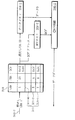
図1は、本発明の実施形態による記憶装置を示すブロック図である。
実施形態として、記憶装置100はコントローラ102とメモリ104とを含む。
コントローラ102は記憶装置100の動作を管理するように構成される回路である。
そして、コントローラ102は、汎用目的プロセッサ(general purpose processor)、デジタル信号プロセッサ(DSP;digital signal processor)、ASIC(application specific integrated circuit)、マイクロコントローラ(microcontroller)、プログラム可能なロジック装置(programmable logic device)、離散回路(discrete circuits)、これらのような装置の組み合わせ等のような要素(components)を含む。
FIG. 1 is a block diagram showing a storage device according to an embodiment of the present invention.
As an embodiment, the
The controller 102 is a circuit configured to manage the operation of the
The controller 102 includes a general purpose processor, a digital signal processor (DSP), an application specific integrated circuit (ASIC), and a micro controller (micro controller). , Discrete circuits, components such as combinations of such devices, and the like.
コントローラ102は、レジスター、キャッシュメモリ、プロセシングコア等のような内部部分(internal portions)を含む。
そして、コントローラ102は、またアドレス及びデータバスインターフェイス、インタラプトインターフェイス等のような外部インターフェイスを含む。
例えば、ただ1つのコントローラ102が記憶装置100内に図示しているが、複数のコントローラが存在することもできる。
また、バッファ、メモリインターフェイス回路、通信インターフェイス等のような他のインターフェイス装置がコントローラ102を内部及び外部要素と接続する記憶装置100の一部分になることができる。
The controller 102 includes internal parts such as a register, a cache memory, a processing core, and the like.
And the controller 102 also includes external interfaces such as address and data bus interfaces, interrupt interfaces, and the like.
For example, although only one controller 102 is shown in
Also, other interface devices such as buffers, memory interface circuits, communication interfaces, etc. can be part of the
他の実施形態として、コントローラ102は、記憶装置100が通信できるようにする回路を含む通信インターフェイスを含むことができる。
例えば、通信インターフェイスには、universal serial bus(USB)、small computer system interface(SCSI)、peripheral component interconnect express(PCIe)、serial attached SCSI(SAS)、parallel ATA(PATA)、serial ATA(SATA)、NVM Express(NVMe)、universal flash storage(UFS)、Fiber channel、Ethernet、remote direct memory access(RDMA)、Infiniband、or other interfaces等が含むことができる。
In other embodiments, the controller 102 can include a communication interface that includes circuitry that enables the
For example, the communication interface, universal serial bus (USB), small computer system interface (SCSI), peripheral component interconnect express (PCIe), serial attached SCSI (SAS), parallel ATA (PATA), serial ATA (SATA), NVM It includes Express (NVMe), universal flash storage (UFS), Fiber channel, Ethernet, remote direct memory access (RDMA), Infiniband, or other interfaces and the like.
このような通信インターフェイスを利用して、記憶装置100は、関連する媒体を通じて外部装置及びシステムと通信するように構成することができる。
他の実施形態として、コントローラ102は、通信インターフェイスを通じて読出し及び書込み要請を受信するように構成することができる。
Utilizing such a communication interface, the
In another embodiment, the controller 102 can be configured to receive read and write requests through the communication interface.
メモリ104は、データを記憶(格納)できる所定の装置である。
ここで、1つのメモリ104が記憶装置100のために図示しているが、複数のメモリが記憶装置100内に含まれることができる。
記憶装置100は、複数の異なるメモリタイプを含むことができる。
The
Here, although one
例として、メモリ104には、dynamic random access memory(DRAM)、DDR、DDR2、DDR3、DDR4のような規格にしたがうdouble data rate synchronous dynamic random access memory(DDR SDRAM)、static random access memory(SRAM)、flash memory、spin−transfer torque magentoresistive random access memory(STT−MRAM)、Phase−Change RAM、nanofloating gate memory(NFGM)、or polymer random access memory(PoRAM)、magnetic or optical mediaのようなnon−volatile memory等を含むことができる。
As an example, the
メモリ104は、データ106、差分圧縮値(differentially compressed values;以下、DCVと記す)108及びマッピングテーブル110を格納(以下、「格納する」で記す)するよう構成される。
後述でさらに詳細に説明するが、メモリ104は複数のメモリ装置を含むことができる。
メモリ104に格納されたデータは、多様な方法でそのような装置の間に分布させることができる。
しかし、説明を簡易にするために、ここではデータは1つのメモリ104に格納されることと説明する。
The
As described in more detail below, the
The data stored in
However, for ease of explanation, it is described here that data is stored in one
コントローラ102は、メモリ104に接続されるメモリインターフェイス111を含む。
コントローラ102は、メモリインターフェイス111を通じてメモリ104にアクセスするよう構成される。
メモリインターフェイス111は、命令、アドレス、及び/又はデータバスのためのインターフェイスを含む。
インターフェイスを通じて、コントローラ102とメモリ104とは通信する。
The controller 102 includes a
The controller 102 is configured to access the
The controller 102 and the
メモリ104がコントローラ102とは別に構成されることを説明したが、他の実施形態ではキャッシュメモリやSRAM等のようなメモリ104の一部分がコントローラ102に含まれてもよい。
コントローラ102は内部通信バスを含む。
プロセシングコア、外部通信インターフェイス、キャッシュメモリ等のような内部要素は内部通信バスを通じて通信することができる。
Although it has been described that the
Controller 102 includes an internal communication bus.
Internal elements such as processing cores, external communication interfaces, cache memories, etc. can communicate over an internal communication bus.
データ106は、記憶装置100に格納されたデータを示す。
後述でさらに詳細に説明するが、DCV108は、関連するデータ106と結合される時、記憶装置100に格納された現在データを示すデータを意味する。
他の実施形態として、DCV108は対応するデータ106のサイズより少ないサイズを有する値である。
例えば、データ106とDCV108とは各々異なるデータサイズを有するページに格納することができる。
例として、データ106のページは8Kバイトのサイズを有する。
これと対照的に、対応するDCV108のためのページのサイズは4Kバイトである。
特定データサイズを例として使用したが、他の実施形態ではデータサイズが異なってもよい。
The
As will be described in more detail below, the
As another embodiment, the
For example, the
As an example, a page of
In contrast, the size of the page for the
Although the specific data size is used as an example, the data size may be different in other embodiments.
コントローラ102は、メモリ104に格納されたデータ106と関連するアドレスに書き込む書込みデータと書込み要請を受信するよう構成される。
マッピングテーブル110は、論理的アドレス、物理的アドレス、DCV「アドレス又は値」等のような情報を有するエントリを含み、「アドレス又は値」又は他の情報間の関連性を作成する。
マッピングテーブル110は、ページ、ブロック、又はハイブリッドマッピング方策を使用することができる。
しかし、ここでの例は説明のためにブロックマッピングを使用する。
The controller 102 is configured to receive write data and a write request to write to an address associated with the
The mapping table 110 includes entries having information such as logical address, physical address, DCV "address or value", etc., to create associations between "address or value" or other information.
The mapping table 110 can use page, block, or hybrid mapping strategies.
However, the example here uses block mapping for purposes of illustration.
コントローラ102は、マッピングテーブル110に格納されたデータを使用して、物理的アドレス、DCV108、又は論理的アドレスと関連されることを職別する。
例えば、通信インターフェイスを通じて論理的アドレスと共に読出し又は書込み要請を受信した後に、コントローラ102はマッピングテーブル110をアクセスして論理的アドレスと関連するエントリを読み出すように構成する。
実施形態として、コントローラ102は、マッピングテーブル110を格納する内部キャッシュメモリにアクセスするよう構成される。
しかし、他の例として、コントローラ102は、DRAMのような外部メモリにアクセスするよう構成されてもよい。
The controller 102 uses the data stored in the mapping table 110 to discriminate between being associated with the physical address, the
For example, the controller 102 may be configured to access the mapping table 110 to read an entry associated with the logical address after receiving a read or write request with the logical address through the communication interface.
In an embodiment, the controller 102 is configured to access an internal cache memory that stores the mapping table 110.
However, as another example, the controller 102 may be configured to access an external memory such as a DRAM.
コントローラ102は、論理的アドレスと関連する物理的アドレスでメモリ104に格納されたデータ106を読み出すよう構成される。
コントローラ102は、書込み要請に含まれた書込みデータ及び物理的アドレスから読み出したデータに基づいてDCV108を計算するように構成される。
この計算は物理的アドレスに格納されたデータ106と入ってくる書込みデータ間の差分に基づいてDCV108を生成する。
また、この計算は物理的アドレスから読み出したデータ及び/又は書込みデータより小さいサイズを有するDCV108を生成する。
The controller 102 is configured to read the
The controller 102 is configured to calculate the
This calculation produces a
This calculation also produces a
DCVは、多様な方法で計算することができる。
実施形態として、コントローラ102は、ソフトウェア又は内部回路内でDCVを計算するよう構成することができる。
DCV機能(109−1)はコントローラ102のこのような動作を示す。
即ち、コントローラ102が書込みデータ及び物理的アドレスから読み出したデータ106を受信した後に、コントローラ102は書込みデータ及びメモリ104からの読出しデータを使用して数学的な計算を遂行することによって、DCVを生成するよう構成される。
DCV can be calculated in various ways.
In embodiments, controller 102 may be configured to calculate DCV in software or internal circuitry.
The DCV function (109-1) indicates such operation of the controller 102.
That is, after the controller 102 receives the write data and the
他の例として、コントローラ102は、外部回路を使用してDCVを計算することができる。
例えば、コントローラ102は、書込みデータ及び読出しデータをDCV回路(109−2)に直接接続する。
そして、コントローラ102は、その応答によりDCVを生成する。
DCV回路(109−2)は、演算ユニット(arithmetic units)、ルックアップテーブル(lookup tables)、入出力バッファ(input/output buffers)等を含むことによって、DCVを計算し、コントローラ102及び/又はメモリ104とインターフェイスする。
As another example, the controller 102 can use external circuitry to calculate DCV.
For example, the controller 102 directly connects the write data and the read data to the DCV circuit (109-2).
Then, the controller 102 generates DCV according to the response.
The DCV circuit (109-2) calculates a DCV by including an arithmetic unit, lookup tables, input/output buffers, etc., and calculates the DCV, and the controller 102 and/or the memory. Interface with 104.
DCV回路(109−2)は、コントローラ102のDCV機能(109−1)に対する代替(alternative)や結合(conjuction)として使用することを示すように点線にて示してある。
DCV回路(109−2)を通じて直接又は間接的にコントローラ102によって遂行される多様な機能はDCVを生成するよう使用される。
The DCV circuit (109-2) is indicated by a dotted line to indicate that it is used as an alternative or a connection to the DCV function (109-1) of the controller 102.
Various functions performed by the controller 102, either directly or indirectly through the DCV circuit (109-2), are used to generate DCV.
実施形態として、機能は簡単な引き算動作(subtraction operation)である。
他の例として、その機能はより複雑なハッシュ関数であってもよい。
他の例として、記録はビットがフリップすることを示すように生成することができる(records can be created indicating which bits have flipped)。
実施形態として、その機能は“diff”関数として称される。
特別な実施形態として、その機能はDCVのサイズを減らすために最適化され得る。
実施形態として、その機能は差分のサイズを減らすために圧縮関数(compression fuction)を含むことができる。
In an embodiment, the function is a simple subtraction operation.
As another example, the function may be a more complex hash function.
As another example, a record can be generated to indicate that bits flip (records can be created indicating while bits have have flipped).
In an embodiment, the function is referred to as the "diff" function.
As a special embodiment, the function can be optimized to reduce the size of the DCV.
In an embodiment, the functionality may include a compression function to reduce the size of the difference.
コントローラ102は、またDCV回路(109−2)を通じて直接又は間接的にDCV関数の逆(inverse)である関数を遂行するよう構成され得る。
逆DCV関数は、ソースデータ及び他のデータから生成されたソースデータ及びDCVを入力として使用して、他のデータを再生成する関数である。
したがって、データ106及びDCV108を維持することによって、他のデータは逆DCV関数を通じて利用する。
The controller 102 may also be configured to perform a function that is the inverse of the DCV function, either directly or indirectly through the DCV circuit (109-2).
An inverse DCV function is a function that uses source data and DCV generated from source data and other data as input and regenerates other data.
Therefore, by maintaining
コントローラ102は、メモリ104に計算されたDCVを格納するよう構成される。
例えば、コントローラ102は、DCV108と共に計算されたDCVをメモリ104に格納することができる。
しかし、後述にてさらに詳細に説明するが、他の実施形態として、DCVはDCV108と共に記憶される前に、メモリ104の1つ又はそれ以上の他の部分にキャッシュされることもできる。
The controller 102 is configured to store the calculated DCV in the
For example, the controller 102 can store the DCV calculated with the
However, as described in further detail below, in other embodiments, the DCV may be cached in one or more other portions of
コントローラ102は、アドレスの関係性を変更させて、アドレスと関連する以前DCVの代わりに計算されたDCVを参照することができる。
後述にてさらに詳細に説明するが、アドレスと関連するデータ106が読み出される時、新しいDCVは以前DCVの代わりにアクセスすることができる。
他の例として、単なる1つのDCVがアドレスと関連するデータを示すように維持することができる。
The controller 102 can change the relationship of the address and refer to the calculated DCV instead of the previous DCV associated with the address.
As will be described in more detail below, when the
As another example, only one DCV can be maintained to show the data associated with the address.
実施形態として、メモリ104の少なくとも一部分は、書込みの観点から、非対称性能(asymmetric performance)を有することができる。
例えば、フラッシュメモリベースの記憶装置は「in−place」書込みを許容しない。
新しいブロックは書込みのために割り当てされなければならない。
そして、次の書込み(future writes)を準備するために、以前ブロックは削除されなければならない。
SMR(shingled magnetic recording)を有する記憶装置で、他のトラックと重なるトラックに書き込むことは、重なるトラック(overlapping track)を再び書き込むことを含む。
後述にてさらに詳細に説明するが、DCVを使用することによって、非対称性能の影響は減らされる。
In embodiments, at least a portion of
For example, flash memory based storage does not allow "in-place" writes.
The new block must be allocated for writing.
The previous block must then be deleted to prepare for the next writes.
In a storage device having SMR (single magnetic recording), writing to a track that overlaps with another track includes rewriting to an overlapping track.
As will be described in more detail below, the use of DCV reduces the impact of asymmetric performance.
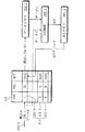
図2A〜図2Eは、本発明の実施形態による記憶装置に対する書込みを説明するための概念図である。
図1の記憶装置100が例として使用される。
図1及び図2Aを参照すると、実施形態として、マッピングテーブル210はメモリ104に格納されたマッピングテーブル210に対応する。
マッピングテーブル210は複数のエントリ211を含む。
各々のエントリ211は、論理的ブロックアドレス(LBA)、物理的ブロックアドレス(PBA)、及びDCVの表示(indication)のためのフィールドを含む。
2A to 2E are conceptual diagrams for explaining writing to the storage device according to the embodiment of the present invention.
The
Referring to FIGS. 1 and 2A, as an embodiment, the mapping table 210 corresponds to the mapping table 210 stored in the
The mapping table 210 includes a plurality of
Each
特定フィールドを例として使用したが、他の実施形態として、他のフィールドが存在することもでき、そのフィールドが他の形態を取ってもよい。
例えば、ここで、論理的及び物理的アドレスはブロックとされるが、他の実施形態では、論理的及び物理的アドレスがブロック内のページ又はメモリ104の他の構造と関連することもできる。
他の例として、物理的アドレスのようなシングルアドレス(single address)は現在唯一のアドレス(the only address present)である。
Although the specific field is used as an example, in other embodiments, other fields may be present and may take other forms.
For example, herein, logical and physical addresses are referred to as blocks, but in other embodiments, logical and physical addresses may be associated with pages within blocks or other structures of
As another example, a single address such as a physical address is currently the only address present.
マッピングテーブル210で、2つのエントリ(211−1、211−2)は以前から存在したエントリである。
新しい論理的ブロックアドレスに書込み要請(202−1)が入力される時、新しいエントリ(211−3)がコントローラ102によって生成される。
この例では、新しいエントリ(211−3)は、論理的ブロックアドレス「1」のためのものである。コントローラ102は論理的ブロックアドレス1と物理的ブロックアドレス23とを関連させる。
In the mapping table 210, two entries (211-1 and 211-2) are entries that existed before.
When a write request (202-1) is input to a new logical block address, a new entry (211-3) is created by the controller 102.
In this example, the new entry (211-3) is for logical block address "1". Controller 102 associates
しかし、物理的ブロックアドレスと関連する唯一のデータは、入力されるデータDである。
例えば、データDは新しいファイルと関連付けされ、DCVは計算されない。
即ち、所定の有効データもデータメモリ(204−1)内の物理的アドレス「23」に存在しない。
DCVフィールドにある‘x’表記はDCVが存在しないか、或いは有効でない表示を示す。
実施形態として、フラッグ(flag)はDCVが存在するか、或いは有効であるかを示す。
他の例として、特定アドレス/フィールド値は、DCVが存在しないか、或いは有効でない表示として定義することができる。
その他の例として、DCVフィールドはエントリ(211−3)の一部ではないこともあり得る。DCVが存在しないか、或いは有効でない表示は他の形態を取ることもあり得る。
However, the only data associated with the physical block address is the incoming data D.
For example, the data D is associated with the new file and the DCV is not calculated.
That is, the predetermined valid data does not exist at the physical address “23” in the data memory (204-1).
The'x' notation in the DCV field indicates that DCV is not present or is not valid.
In an embodiment, a flag indicates whether DCV is present or valid.
As another example, a specific address/field value can be defined as an indication that DCV is not present or is not valid.
As another example, the DCV field may not be part of entry (211-3). The indication that the DCV is not present or is not valid could take other forms.
書込み要請(202−1)が新しいエントリ(211−3)と関連付けされるので、コントローラ102はデータDをデータメモリ(204−1)の物理的ブロックアドレス「23」に格納する。
データメモリ(204−1)は、データ106が格納されるメモリ104の部分を示す。
したがって、新しい有効エントリ(211−3)は、データメモリ(204−1)に格納されたデータを参照して生成される。
データDがデータメモリ(204−1)に書き込まれることとして説明したが、他の実施形態として、多様なバッファーリング又はキャッシング等がデータDをデータメモリ(204−1)に伝送する前に書き込むパート(part)として動作することもできる。
Since the write request (202-1) is associated with the new entry (211-3), the controller 102 stores the data D in the physical block address “23” of the data memory (204-1).
The data memory (204-1) indicates a part of the
Therefore, the new valid entry (211-3) is generated by referring to the data stored in the data memory (204-1).
Although the data D is written to the data memory (204-1), as another embodiment, various buffering, caching, etc. may be performed to write the data D to the data memory (204-1). It can also operate as a (part).
図1及び図2Bを参照すると、実施形態として、新しい書込み要請(202−2)を受信する。
再び、書込み要請(202−2)が論理的ブロックアドレス「1」に直接的に向かう(directed towards)。
しかし、エントリ(211−3)が存在することによって、データは既にデータメモリ(204−1)の関連する物理的ブロックアドレスに格納されている。
即ち、図2AのデータDが格納されている。
したがって、この書込み要請(202−2)は、論理的ブロックアドレス「1」に格納されたデータを新しいデータD’でアップデートする。
Referring to FIGS. 1 and 2B, as an embodiment, a new write request (202-2) is received.
Again, the write request (202-2) goes directly to the logical block address “1” (directed towers).
However, due to the presence of the entry (211-3), the data has already been stored at the associated physical block address in the data memory (204-1).
That is, the data D of FIG. 2A is stored.
Therefore, this write request (202-2) updates the data stored in the logical block address “1” with the new data D′.
データDの元に書込みと対照的に、図2Aと関連して上記で説明したように、データD’はデータメモリ(204−1)の物理的ブロックアドレス「23」に書き込まれない。
コントローラ102はエントリ211がマッピングテーブル210に存在するかを決定する。
実施形態として、コントローラ102は、書込み要請の論理的ブロックアドレスと存在するエントリ211の論理的アドレスを比較する。
仮に合致(match)が発見されれば、以前書込みが発生し、データがデータメモリ(204−1)に存在する。
コントローラ102は、関連する物理的ブロックアドレスに格納されたデータDを読み出す。
ここで、コントローラ102は、物理的ブロックアドレス「23」から読み出す。
図2Aに示したように以前に書き込まれたデータDはデータメモリ(204−1)から読み出される。
In contrast to writing under data D, data D′ is not written to physical block address “23” of data memory (204-1), as described above in connection with FIG. 2A.
The controller 102 determines if the
As an embodiment, the controller 102 compares the logical block address of the write request with the logical address of the existing
If a match is found, a previous write has occurred and the data resides in the data memory (204-1).
The controller 102 reads the data D stored at the associated physical block address.
Here, the controller 102 reads from the physical block address “23”.
As shown in FIG. 2A, the previously written data D is read from the data memory (204-1).
書込み要請(202−2)の新しいデータD’及びデータメモリ(204−1)からの存在するデータDはDCV機能(208−1)の入力として使用される。
DCV機能(208−1)は、上記で説明したように、DCVを計算するために、コントローラ102によって遂行される動作を示す。
DCV機能(208−1)は、新しいデータD’及び存在するデータDに基づいてDCV’を生成する。
ここで、DCV’はデータDと結合されてデータD’を生成することを示すためにアポストロフィを付けた。
コントローラ102は、DCVメモリ(204−2)内に新しいDCV’を格納する。
実施形態として、コントローラ102はDCVアドレスをマッピングテーブル210にあるエントリ(211−3)のDCVフィールドに格納する。
ここで、「0x12」の値はその値が新しいか、変更されたことを示すために、アンダーラインを付けた。
The new data D'of the write request (202-2) and the existing data D from the data memory (204-1) are used as input to the DCV function (208-1).
The DCV function (208-1) indicates the operations performed by controller 102 to calculate DCV, as described above.
The DCV function (208-1) generates DCV' based on the new data D'and the existing data D'.
Here, DCV' is added with an apostrophe to show that DCV' is combined with data D to generate data D'.
The controller 102 stores the new DCV' in the DCV memory (204-2).
As an embodiment, the controller 102 stores the DCV address in the DCV field of the entry (211-3) in the mapping table 210.
Here, the value "0x12" is underlined to indicate that the value is new or changed.
他の例として、DCVメモリ(204−2)は使用されなく、DCV’はエントリ(211−3)のDCVフィールドに格納することができる。
例えば、DCVは相対的に小さく、それでエントリ211にDCVを記憶できるメモリの追加的な量は相対的に小さくなる。
それにも拘らず、エントリ(211−3)は、現在論理的ブロックアドレス、物理的ブロックアドレス、及びDCVを結合(association)する。
As another example, the DCV memory (204-2) is not used and DCV' can be stored in the DCV field of entry (211-3).
For example, the DCV is relatively small, so the additional amount of memory that can store the DCV in
Nevertheless, entry (211-3) associates the current logical block address, physical block address, and DCV.
図1及び図2Cを参照すると、実施形態として、他の書込み要請(202−3)がコントローラ102によって入力される。
この書込み要請(202−3)は、論理的ブロックアドレス「1」に新しいデータD”を書き込むための要請である。
再び、コントローラ102はマッピングテーブル210で合致(match)を見つけようとする。
ここで、エントリ(211−3)が存在する。
図2Bと同様に、コントローラ102は、エントリ(211−3)で表示された物理的ブロックアドレス「23」からデータDを読み出す。
データDは、データメモリ(204−1)から出力される。
データメモリ(204−1)から出力された、書込み要請(202−3)の新しいデータD”と、存在するデータDはDCV機能(208−1)に対する入力として使用される。
Referring to FIGS. 1 and 2C, as another embodiment, another write request (202-3) is input by the controller 102.
This write request (202-3) is a request for writing new data D″ to the logical block address “1”.
Again, the controller 102 tries to find a match in the mapping table 210.
Here, the entry (211-3) exists.
As in FIG. 2B, the controller 102 reads the data D from the physical block address “23” displayed in the entry (211-3).
The data D is output from the data memory (204-1).
The new data D″ of the write request (202-3) output from the data memory (204-1) and the existing data D are used as an input to the DCV function (208-1).
DCV機能(208−1)は、新しいデータD”と存在するデータDに基づいて新しいDCV”を生成する。
特に、DCV”の生成は、図2Bで書き込まれたデータD’の中間状態(intermediate state)に関与しない。
データDが物理的ブロックアドレス「23」でデータメモリ(204−1)に格納されたデータであるので、関心の差(difference of interest)はデータDと書き込まれるデータD”との間の差である。
コントローラ102は、結果であるDCV”をDCVメモリ(204−2)に格納する。
コントローラ102は、エントリ(211−3)のDCVフィールドにあるDCVアドレスを使用して、予め存在するDCV’を新しいDCV”で重なって書き込む。
したがって、現在エントリ(211−3)にあるDCVフィールドは新しいDCV”を参照する(references)。
The DCV function (208-1) generates new DCV" based on the new data D" and the existing data D".
In particular, the generation of DCV″ does not involve the intermediate state of the data D′ written in FIG. 2B.
Since the data D is the data stored in the data memory (204-1) at the physical block address “23”, the difference of interest is the difference between the data D and the written data D″. is there.
The controller 102 stores the resulting DCV″ in the DCV memory (204-2).
The controller 102 uses the DCV address in the DCV field of the entry (211-3) to write the pre-existing DCV' with the new DCV'' in an overlapping manner.
Therefore, the DCV field currently in the entry (211-3) refers to the new DCV" (references).
図1及び図2Dを参照すると、その動作は図2Cで説明したものと類似する。
しかし、実施形態として、DCV”をDCVメモリ(204−2)に書き込めば、新しいDCVアドレスが生成される。
例えば、仮にDCVメモリ(204−2)がフラッシュメモリで具現されれば、新しいDCV”はDCV’を格納するページと異なる、DCVメモリ(204−2)にあるページに書き込まれる。
新しいDCVアドレスはDCVメモリ(204−2)にあるアドレスであり、DCV”はそこに格納される。エントリ(211−3)で、新しいアドレスは「0x21」で表示され、DCVフィールドで変更を示すようにアンダーラインを付けた。
1 and 2D, the operation is similar to that described in FIG. 2C.
However, as an embodiment, writing DCV″ to the DCV memory (204-2) will generate a new DCV address.
For example, if the DCV memory 204-2 is implemented by a flash memory, the new DCV″ is written in a page in the DCV memory 204-2 different from the page storing DCV′.
The new DCV address is the address in the DCV memory (204-2) and the DCV" is stored there. At entry (211-3), the new address is displayed as "0x21" and indicates the change in the DCV field. To underline.
DCVメモリ(204−2)にある同一アドレスでメモリ位置(memory location)をアップデートするか、或いはエントリ(211−3)を新しいアドレスにアップデートすることが、論理的ブロックアドレスとDCVの関連性(association)を変更する方法の例として使用して新しいDCVを参照することにも拘らず、その関連性においての変更が異なる。
例えば、実施形態として、コントローラ102は、DCVフィールドのような、マッピングテーブルにDCV”を格納する。
エントリ(211−3)に格納されたDCV’はDCV”と取り替える。
Updating the memory location with the same address in the DCV memory (204-2) or updating the entry (211-3) with a new address may result in an association between the logical block address and the DCV. ) Is used as an example of how to change and refer to a new DCV, but the change in its relevance is different.
For example, in an embodiment, the controller 102 stores DCV″ in a mapping table, such as the DCV field.
DCV′ stored in the entry (211-3) is replaced with DCV″.
図1及び図2Eを参照すると、実施形態として、コントローラ102は、DCVフラッシュアクセス(202−4)を受信する。
ここで、DCVフラッシュアクセス(202−4)は、上記で説明した各図と同様に、論理的ブロックアドレス「1」を示す。
マッピングテーブル210は、図2Dのマッピングテーブル210と同様に、初期状態(210−1)にある。
再び、コントローラ102はエントリ(211−3)にアクセスし、データメモリ(204−1)にある関連する物理的ブロックアドレス「23」からデータDを読み出す。
しかし、コントローラ102は、DCVフィールドを使用して、DCVメモリ(204−2)に格納されたDCV”にアクセスする。
ここで、コントローラ102は、DCVアドレスを使用してDCVメモリ(204−2)にアクセスする。
Referring to FIGS. 1 and 2E, in an embodiment, the controller 102 receives a DCV flash access (202-4).
Here, the DCV flash access (202-4) indicates the logical block address “1” as in the above-described drawings.
The mapping table 210 is in the initial state (210-1) like the mapping table 210 of FIG. 2D.
Again, the controller 102 accesses the entry (211-3) and reads the data D from the associated physical block address "23" in the data memory (204-1).
However, the controller 102 uses the DCV field to access the DCV" stored in the DCV memory (204-2).
Here, the controller 102 uses the DCV address to access the DCV memory (204-2).
コントローラ102は、DCV”及びデータDを逆DCV機能(208−2)に提供する。
逆DCV機能(208−2)は、上記で説明したように、データとDCVとを組み合わせてデータアップデートされたバージョンを作るための関数を示す。
ここで、逆DCV機能(208−2)は、データDとDCV”とを使用してデータD”を再生成する。
コントローラ102は、データDの代わりにデータメモリ(204−1)にデータD”を格納する。
マッピングテーブル210は、状態(210−2)にアップデートされる。
ここで、エントリ(211−3)は、有効DCVが存在しないことを示すようにアップデートされる。
したがって、論理的ブロックアドレス「1」に連続された書込みが、図2Bで説明したように、コントローラ102によって取り扱われる。
Controller 102 provides DCV" and data D to the inverse DCV function (208-2).
The inverse DCV function (208-2) represents a function for combining data and DCV to create a data updated version, as described above.
Here, the inverse DCV function (208-2) regenerates the data D″ using the data D and the DCV″.
The controller 102 stores the data D″ in the data memory (204-1) instead of the data D.
The mapping table 210 is updated to the state (210-2).
Here, the entry (211-3) is updated to indicate that there is no valid DCV.
Therefore, consecutive writes to logical block address "1" are handled by controller 102, as described in FIG. 2B.
上記で説明した動作の結果として、頻繁に変更されたデータは非対称性能を有するメモリ104を有する記憶装置の性能において影響を与える。
例えば、持続的に変更されたデータは、全体データセットの5%未満を含み得る。
例として200GBを使用すれば、単なる1%又は2GBが持続的にアップデートされる。
DCVのより小さいサイズは書き込まれるデータの量を減少させる。
実施形態として、大部分のDCVは全体データブロックのサイズの20%である(a majority of DCV may be on the order of 20% of a size of an entire block of data)。
As a result of the operations described above, frequently modified data impacts the performance of storage
For example, persistently modified data may comprise less than 5% of the total data set.
Using 200 GB as an example, only 1% or 2 GB is continuously updated.
The smaller size of DCV reduces the amount of data written.
As an example, most DCVs are 20% of the size of the entire data block (a majority of DCV may be on the order of 20% of a size of an entry block of data).
余りの大部分は相変わらず、データのサイズの50%より小さい。
したがって、200GBの例で、DCVの400MBないしは1GBが書き込まれる。
減られたサイズは空間を効率的に作り、浪費を減らす。
特に、2GBの新しく削除されたブロックを使用してアップデートするのに、現在では400MBを使用することができる。
記憶装置の与えられた容量に対して、新しく削除されたブロックに対する要求を減らすことはガーベッジコレクションの遂行頻度を減らし、媒体に対する消耗度を減らす。
Most of the remainder is still smaller than 50% of the size of the data.
Therefore, in the example of 200 GB, 400 MB or 1 GB of DCV is written.
The reduced size creates space efficiently and reduces waste.
In particular, 400 MB can currently be used to update with 2 GB of newly deleted blocks.
For a given amount of storage, reducing the demand for newly deleted blocks reduces the frequency with which garbage collection is performed and reduces media consumption.
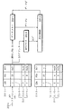
図3A〜図3Eは、本発明の実施形態による記憶装置から読み出す動作を説明するための概念図である。
図1の記憶装置100が例として使用される。図2A〜図2Eの構成要素と類似する構成要素の説明は簡易化のために省略する。
図1及び図3Aを参照すると、マッピングテーブル310は、図2Aで説明したように、データが書き込まれた後の状態を示す。
即ち、データDはデータメモリ(304−1)内に格納され、エントリ(311−3)はマッピングテーブル310に追加される。
しかし、エントリ(311−3)はDCVが存在しないか、或いは有効ではない表示を含む。
3A to 3E are conceptual diagrams for explaining the operation of reading from the storage device according to the embodiment of the present invention.
The
Referring to FIGS. 1 and 3A, the mapping table 310 indicates a state after data has been written, as described with reference to FIG. 2A.
That is, the data D is stored in the data memory (304-1), and the entry (311-3) is added to the mapping table 310.
However, entry (311-3) contains an indication that the DCV is not present or is not valid.
コントローラ102は、読出し要請302を受信する。
ここで、読出し要請302は、論理的ブロックアドレス「1」にアクセスするように構成される。これに応答し、コントローラ102は、マッピングテーブル310をアクセスするか、或いは物理的ブロックアドレス「23」を読み出す。
物理的ブロックアドレスを使用して、コントローラ102はデータメモリ(304−1)からデータDを読み出す。
コントローラ102は、データDと共に読出し要請302に応答する。
特に、エントリ(311−3)はDCVが存在しないか、或いは有効ではない表示を含むので、コントローラ102は、変更(modification)無しでデータDを応答する。
The controller 102 receives the read
Here, the
The controller 102 reads the data D from the data memory (304-1) using the physical block address.
The controller 102 responds to the read
In particular, the entry (311-3) contains an indication that the DCV does not exist or is not valid, so the controller 102 responds with the data D without modification.
図1及び図3Bを参照すると、実施形態として、マッピングテーブル310が図2Bで説明したようにデータが書き込まれた後の状態であるので、読出し要請302はコントローラ102によって受信される。
即ち、データDは、初期にデータメモリ(304−1)に書き込まれ、DCVメモリ(304−2)に格納されているので、アップデートされたデータD’が書き込まれる。
したがって、コントローラ102は、読出し要請302を再び受信し、これに応答して、物理的ブロックアドレス「23」をアクセスすることによってデータメモリ(304−1)からデータDを読み出す。
しかし、有効DCVフィールドがエントリ(311−3)に存在するので、コントローラ102はDCVメモリ(304−2)にアクセスしてDCV’を読み出す。
コントローラ102は、逆DCV機能(308−2)に対する入力としてデータDとDCV’を使用し、データDとDCV’とを組み合わせてデータD’を生成する。
コントローラ102は、データD’と共に読出し要請302に応答する。
Referring to FIGS. 1 and 3B, the
That is, since the data D is initially written in the data memory (304-1) and stored in the DCV memory (304-2), the updated data D′ is written.
Therefore, the controller 102 receives the read
However, since the valid DCV field exists in the entry (311-3), the controller 102 accesses the DCV memory (304-2) and reads DCV'.
The controller 102 uses the data D and DCV' as inputs to the inverse DCV function (308-2) and combines the data D and DCV' to generate the data D'.
The controller 102 responds to the read
増加した読出し量がこの技術に関与する間に、その増加した読出し量は、無視できないが、少ない量を有する。
例えば、実施形態として、メモリ104の内部読出し幅(internal read bandwidths)は、記憶装置100の外部インターフェイス幅より高い。
たとえば、読出し性能に無視できない影響を有しても、読出しは削除されたブロックの使用、隣接するトラックの再書込み等をもたらしない。
このように、読出し性能を減らす動作は、レイテンシを減らすか、或いはレイテンシの一貫性を向上させるか、あるいは、その他の関連する動作より影響が少ない。
While the increased read volume is involved in this technique, the increased read volume has a small but not negligible amount.
For example, in an embodiment, the internal read widths of the
For example, reading does not result in the use of deleted blocks, rewriting of adjacent tracks, etc., although it has a non-negligible effect on read performance.
As such, operations that reduce read performance reduce latency or improve latency consistency, or have less impact than other related operations.
図1及び図3Cを参照すると、実施形態として、読出し要請302は、マッピングテーブル310が図2Cに示したようにデータが書き込まれた後の状態にある時、コントローラ102によって受信される。
即ち、データDは、初期にデータメモリ(304−1)に書き込まれる。
アップデートされたデータD’は、DCVメモリ(304−2)に格納されてあるDCV’の結果として書き込まれる。
そして、追加してアップデートされたデータD”は、DCVメモリ(304−2)に格納されてあるDCV”の結果として書き込まれる。
Referring to FIGS. 1 and 3C, in an embodiment, the
That is, the data D is initially written in the data memory (304-1).
The updated data D'is written as a result of the DCV' stored in the DCV memory (304-2).
Then, the additionally updated data D″ is written as a result of the DCV″ stored in the DCV memory (304-2).
コントローラ102は、再び物理的ブロックアドレス23のためのエントリ(311−3)にアクセスし、物理的ブロックアドレス「23」を使用してデータメモリ(304−1)にアクセスしてデータDにアクセスし、DCVアドレスを使用してDCVメモリ(304−2)をアクセスする。
しかし、データD”が論理的ブロックアドレス「1」に最も最近に書き込まれたデータであるので、DCV”は利用可能であり、DCVメモリ(304−2)でアクセスされるDCVである。
コントローラ102は、DCV”とデータDを逆DCV機能(308−2)に対する入力として使用してデータD”を生成する。
コントローラ102は、データD”と読出し要請302とに応答する。
したがって、初期データDがアクセスされたが、最も最近データD”は再び生成される。
特に、データD’とそれと関連するDCV’は、データD”を生成するのに使用されない。
The controller 102 again accesses the entry (311-3) for the
However, since the data D″ is the data most recently written to the logical block address “1”, the DCV″ is available and is the DCV accessed by the DCV memory (304-2).
Controller 102 uses data DCV" and data D as inputs to the inverse DCV function (308-2) to generate data D".
The controller 102 responds to the data D″ and the read
Therefore, although the initial data D has been accessed, the most recent data D″ is regenerated.
In particular, data D'and its associated DCV' are not used to generate data D".
図3A〜図3Cで説明したように、コントローラ102は、DCVフィールドがDCVが存在するか、又は有効であるかを指示するか否かに基づいて、異なった動作するように構成される。
しかし、他の実施形態として、コントローラ102は、たとえ初期データがデータメモリ(304−1)に格納されている時にも、図3B及び図3Cと同様に動作するように構成され得る。
特に、エントリ311のDCVフィールドは、DCVフィールドにあるか、或いはDCVメモリ(304−2)内にある識別DCV(identityDCV)を指示することで初期化される。
識別DCVは、初期データDと共に逆DCV機能(308−2)に対する入力で使用される時、データDを発生する。
結果として、実際データを比較することから得られるDCVが存在するか、或いは有効であるか否かに関係なく、実質的に同一の動作がコントローラ102によって遂行される。
As described in FIGS. 3A-3C, the controller 102 is configured to operate differently based on whether the DCV field indicates whether DCV is present or valid.
However, in other embodiments, the controller 102 may be configured to operate similarly to FIGS. 3B and 3C even when the initial data is stored in the data memory (304-1).
In particular, the DCV field of
The identification DCV produces the data D when used at the input to the inverse DCV function (308-2) with the initial data D.
As a result, substantially the same operation is performed by controller 102 regardless of whether the DCV resulting from comparing the actual data is present or valid.
図1及び図3Dを参照すると、実施形態として、データの以前の初期バーションにアクセスすることができる。
特に、コントローラ102は、ソース読出し要請(302−1)を受信する。
ここで、ソース読出し要請(302−1)は、論理的ブロックアドレス「1」を参照する。
その応答で、コントローラ102は、図3Aで説明したアクセスと同様に、データメモリ(304−1)の物理的ブロックアドレス「23」にあるデータDにアクセスする。
しかし、エントリ(311−3)のDCVフィールドは、図3B及び図3Cと同様に有効である。
即ち、論理的ブロックアドレス「1」には、データのアップデートバージョンが存在する。
図3Bと図3Cとは対照的に、初期データDは、再び生成された現在データD’又はD”に復帰する(returned)。
したがって、ソース読出し要請(302−1)又は同様の要請を使用して、記憶装置100に格納されたデータの以前のバーションを読み出すことができる。
エントリ(311−3)のDCVフィールドからのDCVアドレスを読み出す動作が例として使用される反面、他の実施形態として、DCV値はエントリ(311−3)のDCVフィールドから読み出されてもよい。
例えば、図3B及び図3CのDCV’及びDCV”は各々エントリ(311−3)から読み出される。
Referring to FIGS. 1 and 3D, as an embodiment, a previous initial version of the data can be accessed.
In particular, the controller 102 receives the source read request (302-1).
Here, the source read request (302-1) refers to the logical block address “1”.
In response to this, the controller 102 accesses the data D at the physical block address “23” of the data memory (304-1), similar to the access described in FIG. 3A.
However, the DCV field of entry (311-3) is valid as in FIGS. 3B and 3C.
That is, an updated version of data exists at the logical block address “1”.
In contrast to FIGS. 3B and 3C, the initial data D is returned to the regenerated current data D′ or D″.
Therefore, the source read request (302-1) or a similar request can be used to read the previous version of the data stored in the
While the operation of reading the DCV address from the DCV field of entry (311-3) is used as an example, the DCV value may be read from the DCV field of entry (311-3) as another embodiment.
For example, DCV′ and DCV″ in FIGS. 3B and 3C are read from the entry (311-3), respectively.
図1及び図3Eを参照すると、実施形態として、図2Cで説明したようにマッピングテーブル310がデータが書き込まれた後の状態にある時、読出し要請(302−2)がコントローラ102によって入力される。
即ち、データDは初期にデータメモリ(304−1)に書き込まれる。
アップデートされたデータD’は、DCVメモリ(304−2)に格納されてあるDCV’の結果として書き込まれる。
そして、追加して、アップデートされたデータD”は、DCVメモリ(304−2)に格納されてあるDCV”の結果として書き込まれる。
しかし、この実施形態で、1つ又はそれ以上の中間DCVs(intermediate DCVs)が維持される。
この例で、DCV”は現在のDCVである。
しかし、DCV’は、また維持される。
エントリ(311−4)にある「0x55」の追加的なパラメーターはDCV’の表示を示す(例えば、その値やアドレス)。
Referring to FIGS. 1 and 3E, as an embodiment, a read request 302-2 is input by the controller 102 when the mapping table 310 is in a state after data is written as described with reference to FIG. 2C. ..
That is, the data D is initially written in the data memory (304-1).
The updated data D'is written as a result of the DCV' stored in the DCV memory (304-2).
Then, additionally, the updated data D″ is written as a result of the DCV″ stored in the DCV memory (304-2).
However, in this embodiment, one or more intermediate DCVs (intermediate DCVs) are maintained.
In this example, DCV" is the current DCV.
However, DCV' is also maintained.
The additional parameter "0x55" in entry (311-4) indicates the indication of DCV' (eg its value or address).
この例で、読出し要請(302−2)はLBA1’のための要請である。
LBA1’はデータD’としてのデータの状態を示す。
したがって、コントローラ102は、DCV’アドレス、即ちDCV’がDCVメモリ(304−2)に格納された位置を示すアドレスにアクセスする。
結果として、DCV’はアクセスされ、逆DCV機能(308−2)にあるデータDと結合されてデータD’を生成する。
たとえとして単なる1つの中間DCV(例えば、DCV’)が例として使用されるが、他の実施形態としていくつかの数の中間DCVも格納されることができる。
例えば、DCVs、DCV’、DCV”、DCV’’’、及びDCV’’’’がDCVメモリ(304−2)に全て格納されるDCVsの各々は、データDと結合されてデータD’、D”、D’’’、及びD’’’’のようなデータの以後バーションを各々生成することができる。
In this example, the read request (302-2) is a request for LBA 1'.
LBA1' indicates the state of data as data D'.
Therefore, the controller 102 accesses the DCV' address, that is, the address indicating the position where the DCV' is stored in the DCV memory (304-2).
As a result, DCV' is accessed and combined with data D in the inverse DCV function (308-2) to produce data D'.
As an analogy, only one intermediate DCV (eg, DCV′) is used as an example, but some other number of intermediate DCVs may also be stored in other embodiments.
For example, DCVs, DCV', DCV", DCV'", and DCV"" are all stored in the DCV memory (304-2). Each of the DCVs is combined with the data D to obtain the data D', D. Subsequent versions of data such as ", D'", and D"" can be generated respectively.
図4A及び図4Bは、本発明の他の実施形態による記憶装置を概略的に示すブロック図である。
図4Aを参照すると、実施形態として、記憶装置400は、図1に示した記憶装置100のコントローラ102と同様のコントローラ402とを含む。
しかし、記憶装置400は、不揮発性メモリ(404−1)と揮発性メモリ(404−2)とを含む。
不揮発性メモリ(404−1)には例として、flash memory、STT−MRAM、Phase−ChangeRAM、NFGM、or PoRAM、magnetic or optical media等が含まれ得る。
揮発性メモリ(404−2)には例として、DRAM、DDR、DDR2、DDR3、DDR4、SRAM等のような多様な標準にしたがうDDR SDRAM等が含まれ得る。
4A and 4B are block diagrams schematically illustrating a storage device according to another embodiment of the present invention.
Referring to FIG. 4A, as an embodiment, the
However, the
The non-volatile memory (404-1) may include, for example, flash memory, STT-MRAM, Phase-Change RAM, NFGM, or PoRAM, magnetic or optical media, and the like.
Volatile memory (404-2) may include, by way of example, DDR SDRAM, etc., according to various standards such as DRAM, DDR, DDR2, DDR3, DDR4, SRAM, and the like.
コントローラ402は、不揮発性メモリ(404−1)にデータ406を記憶し、揮発性メモリ(404−2)にDCV408を格納する。
コントローラ402は、また揮発性メモリ(404−2)にマッピングテーブル410を格納する。
実施形態として、記憶装置400の使用は、一貫性(consistency)よりは一貫されたレイテンシ(consistent latency)に優先順位を置く。
したがって、データの一貫性は次順位になる(consistency of the data may be relaxed)。
例えば、様々なインターネット−スケールアプリケーション(several internet−scale applications)は次順位範囲内で(within relaxed bounds)一貫性を考慮してアクセスされる。
そのようなアプリケーションは、ツイート(tweets)及びフォトタギング(photo tagging)を含む。
The controller 402 stores the
The controller 402 also stores the mapping table 410 in the volatile memory (404-2).
In an embodiment, the use of
Thus, the consistency of the data is second order (consistency of the data may be relaxed).
For example, various internet-scale applications are accessed for consistency with within relaxed bounds.
Such applications include tweets and photo tagging.
しかし、そのようなアプリケーションのために、レイテンシスパイク(latency spikes)は受け入れない。
DCV408で表現されるように、このような範囲内のデータは、揮発性メモリ(404−2)に格納される。
コントローラ402は、DCV408のオーバープロー(overflows)を不揮発性メモリ(404−1)にフラッシュ(flush)するようにする。
実施形態として、コントローラ402はDCV408を不揮発性メモリ(404−1)のデータ406にフラッシュする。
However, for such applications, it does not accept latency spikes.
Data within such a range, as represented by DCV 408, is stored in volatile memory (404-2).
The controller 402 causes the DCV 408 overflows to be flushed into the non-volatile memory (404-1).
In an embodiment, controller 402 flushes DCV 408 to
揮発性メモリ(404−2)はバッテリ、スーパーキャパシタ、又はNVRAMによってバックアップされる(may be backed)。
しかし、実施形態として、そのようなバックアップは、DCV408の損失を生じる失敗が相変わらず、許容可能な範囲内にあるので、必ず必要であることではない。
バックアップのために使用されるバッテリ、スーパーキャパシタ、又はNVRAMを省略すれば、記憶装置400の費用(cost)を減少させることができる。
Volatile memory (404-2) may be backed by a battery, supercapacitor, or NVRAM.
However, as an embodiment, such backup is not absolutely necessary because the failure to cause loss of DCV 408 is still within an acceptable range.
By omitting the battery, supercapacitor, or NVRAM used for backup, the cost of the
実施形態として、キャッシュ412は、データを不揮発性メモリ(404−1)に伝送する前に、データをキャッシュするのに使用される。
例えば、図2A〜図2Dで説明した読出し要請から追い出されたデータは、キャッシュ412に格納される。
このストレージは、図2A〜図2Dで説明した多様な技術無しでも動作することができる。しかし、データがキャッシュ412から追い出される時又はそれと同様な場合に、図2A〜図2Dで説明した技術が使用することができる。
特別な例として、キャッシュ412に格納されたデータブロックは、複数の読出し要請によってアップデートされる。
このようなアップデートは、DCVの計算に関係しない。
データブロックがデータを追い出されるか、或いはコミットされる時、データの状態に基づいて図2A〜図2Dで説明したようにDCVを生成する。
In an embodiment, the
For example, the data evicted from the read request described with reference to FIGS. 2A to 2D is stored in the
This storage can operate without the various techniques described in FIGS. 2A-2D. However, the techniques described in FIGS. 2A-2D can be used when data is evicted from
As a special example, the data block stored in the
Such updates are not relevant to the calculation of DCV.
When a data block is flushed or committed with data, DCV is generated based on the state of the data as described in FIGS. 2A-2D.
図4Bを参照すると、実施形態として、記憶装置401は図4Aの記憶装置400と同様である。
しかし、記憶装置401では、コントローラ402はキャッシュされたDCV(408−1)として表現される揮発性メモリ(404−2)内DCVをキャッシュするようにする。
特に、コントローラ402は、頻繁にアクセスされるDCVを揮発性メモリ(404−2)に維持する。
コントローラ402は、キャッシングアルゴリズムや発見的な方法(heuristics)等を使用して、どのキャッシュされたDCV(408−1)を維持するかを決定する(determine which DCVs 408−1 to maintain in the cache)。
コントローラ402は、他のキャッシュされたDCV(408−1)を不揮発性メモリ(404−1)に格納されたDCV(408−2)に伝送し、その逆も成立する。
結果的に、実施形態として、頻繁にアクセスされるか、或いは重くアクセスされるデータはキャッシュされる。
さらに、キャッシュされたDCV(408−1)は、対応するデータ406よりサイズが小さいので、実際のデータがキャッシュされた場合よりも、より多くのアップデートが揮発性メモリ(404−2)で維持される。
Referring to FIG. 4B, as an embodiment, the
However, in the
In particular, the controller 402 maintains frequently accessed DCVs in volatile memory (404-2).
The controller 402 uses a caching algorithm or heuristics to determine which cached DCV (408-1) to maintain (determine while DCVs 408-1 to maintain in the cache). ..
The controller 402 transmits the other cached DCV (408-1) to the DCV (408-2) stored in the non-volatile memory (404-1) and vice versa.
Consequently, in embodiments, data that is frequently accessed or heavily accessed is cached.
Further, because the cached DCV (408-1) is smaller in size than the corresponding
図5は、本発明の実施形態による記憶装置内のページデータサイズを示す図ある。
実施形態として、データページ502とDCVページ504とは同じメモリ500に格納される。
ここで、データページ(502−1、502−2)とDCVページ(504−1)〜(504−4)とはメモリ500に格納されたデータページ502及びDCVページ504の例である。
ここで、DCVページ504はソースデータと比較して相対的にさらに小さいサイズのDCVを示すためにさらに小さく示している。
この例で、DCVページ504はデータページ502の半分サイズである。
しかし、他の実施形態では、DCVページ504のデータサイズは使用された特別なDCV機能によって異なり得る。
FIG. 5 is a diagram showing a page data size in the storage device according to the embodiment of the present invention.
As an embodiment, the
Here, the data pages (502-1, 502-2) and the DCV pages (504-1) to (504-4) are examples of the
Here, the
In this example,
However, in other embodiments, the data size of the
実施形態として、データページ502及びDCVページ504の両方はレイテンシを増加させる順次書込み(in−place writes)の不足のような、同一の制限を受け得る。
上記で説明したように、データページ502は一般的にDCVが変わる間は維持される。
DCVページに対する変化は、レイテンシ影響(latency impact)をもたらす。
しかし、DCVページ504のサイズが段々小さくなることによって、レイテンシ影響は減少される。
例えば、DCVページ504がデータページ502と異なるブロックに格納される。
したがって、さらに多くのDCVがDCVページ504に蓄積されることによって、ガーベッジコレクションがそのブロックで遂行されて自由ブロックが回復する(recover)。
DCVページ504がさらに小さいので、ガーベッジコレクションはより少ない時間で遂行されるか、及び/又はより少ない頻度で遂行される。
In embodiments, both
As explained above, the
Changes to the DCV page result in latency impact.
However, as the size of the
For example,
Therefore, as more DCV is stored in
Garbage collection may be performed in less time and/or less frequently because the
これに加えて、データページ502はDCVページ504より長い間、有効な状態を維持する。
結果的に、データページ502を格納するブロックはDCVページ504を格納するブロックよりもガベージコレクションを受けにくい。
また、DCVページ504が早く無効化される可能性がより高いので、DCVページ504を格納するブロックのより多くのページが無効となり、ガベージコレクション操作の時間が短縮される。
In addition,
As a result, the block storing
Also, because
図6は、本発明の実施形態によるSSDを示すブロック図である。
実施形態として、SSD600は図1に図示された記憶装置100のコントローラ102と同様である。
しかし、SSD600は、フラッシュメモリ(604−1)、DRAM(604−2)、及びSRAM(604−3)を含む。
コントローラ602は、フラッシュメモリ(604−1)にデータ606とDCV(608−1)とを格納する。
例えとして、メモリの構成を特定して示しているが、他の実施形態として、SSD600はデータ606及びDCV(608−1、608−2)の構成と分布が他のメモリを含むことができ、マッピングテーブル610も異なることができる。例えば、SSD600は図1、図4A、及び図4Bと同様な構成を有する。
FIG. 6 is a block diagram illustrating an SSD according to an exemplary embodiment of the present invention.
As an embodiment, the
However, the
The controller 602 stores the
For example, although the configuration of the memory is specifically shown, in another embodiment, the
フラッシュメモリ(604−1)に格納されたデータ606とDCV(608−1)はガーベッジコレクションを頻繁に受けやすい(susceptible to garbage collection)。
データ606とDCV(608−1)とを格納するページが削除され、潜在的に追加的なレイテンシを招く。
しかし、先に説明したように、DCV(608−1)のサイズは対応するデータ606より小さい。
即ち、データ606を格納するために使用されるフラッシュメモリ(604−1)内のページはDCV(608−1)を格納するのに使用されるページよりサイズが大きい。
DCVを使用すれば、SSD600内で書込み変更(write modifications)、即ち非順次アップデート(out−of−place updates)が減少する。これはリクレーム(reclaim)される無効ブロックを小さくする。
The
The page that stores
However, as explained above, the size of DCV (608-1) is smaller than the corresponding
That is, the page in flash memory (604-1) used to store
The use of DCV reduces write modifications, or out-of-place updates, in
これによって、ガーベッジコレクションの回数(freuency)が減少する。
特に、SSD600は、ビックデータとクラウドアプリケーションとアップデート−ヘビーI/Oトラフィックを処理する。
例えば、SSD600は、アップデータとクラウドアプリケーションとを有し、ガーベッジコレクションの低い回数とそれによる高いレイテンシの低い機会、特にレイテンシスパイクを有し、アップデート−ヘビーI/Oトラフィックを処理する。
This reduces the frequency of garbage collection.
In particular,
For example, the
特に、データ606に対する書込みアップデートをする時、データ606の第1コピーはフラッシュメモリ(604−1)に残る。
フラッシュメモリ(604−1)にあるDCV(608−1)とDRAM(604−2)にキャッシュされたフラッシュDCV(608−2)は、書込みアップデートがヘビーな作業負荷(heavy workloads)であっても、フラッシュメモリ(604−1)にあるページの寿命を増加させる。
これに加えて、先に説明したように、データ606の以前バージョンも利用することができる。
レイテンシを向上させることのみならず、アーキテクチャがフラッシュセル消耗(wearing)を改善することもできる。
In particular, when performing a write update on the
The DCV (608-1) in the flash memory (604-1) and the flash DCV (608-2) cached in the DRAM (604-2) have a heavy write load even if the write update is a heavy workload. , Increase the lifespan of pages in the flash memory (604-1).
In addition to this, earlier versions of the
Not only can the latency be improved, but the architecture can also improve flash cell wear.
特に、以前ページを無効化し、アップデートデータのための新しいページを要請する代わりに、コントローラ602は、以前ページとアップデートとの間の差分を示すDCVと共にフラッシュメモリ(604−1)に有効/アクティブとして以前ページを維持する。
続く読出し動作の時に、コントローラ602は、以前ページとDCVとを全て読み出し、結合してデータページまで大部分を提供する。
上記で説明したように、DCVをどこに記憶するかについては多数の構成がある。
例えば、フラッシュメモリ(604−1)、DRAM(604−2)、SRAM(604−3)、又はそのようなメモリの組み合わせに格納する。
これに加えて、アクティブ又は“ホット”ページDCVをDRAM(604−2)にキャッシュし、フラッシュメモリ(604−1)上のDCV(608−1)に持続的な(persistent)コピーを維持することによって、DCVはキャッシュされる。
In particular, instead of invalidating the previous page and requesting a new page for the update data, the controller 602 may activate/activate the flash memory (604-1) with DCV indicating the difference between the previous page and the update. Keep the page before.
During a subsequent read operation, controller 602 reads all previous pages and DCV and combines them to provide the majority of the data page.
As explained above, there are numerous configurations for where to store the DCV.
For example, it is stored in flash memory (604-1), DRAM (604-2), SRAM (604-3), or a combination of such memories.
In addition, cache an active or "hot" page DCV in DRAM (604-2) and maintain a persistent copy in DCV (608-1) on flash memory (604-1). Causes the DCV to be cached.
実施形態として、読出しと書込みが非対称(asymmetric)でないか、同一のオーバーヘッドを有するか、或いはそのようなものである時でも、本明細書で説明したように、記憶装置は性能利点を有する。
特に、仮に書込みのサイズとDCVのデータサイズとを有する書込み時間スケール(write times scale)が対応するデータブロックのデータサイズより小さければ、書込み時間は減少する。
実施形態として、DRAM(604−2)は、書込み要請及び/又は書込みデータをキャッシュするのに使用することができる。
書込み要請を処理することがデータ606に存在するデータを読み出すことに関与する時、対応するデータ606はキャッシュされたデータ(606−1)としてDRAM(604−2)に格納される。
コントローラ602は、上記で説明したDCV関数に対する入力として、DRAM(604−2)に格納されたキャッシュされたデータ(606−1)を使用する。
即ち、フラッシュメモリ(604−1)に格納されたデータ606からデータを読み出す代わりに、コントローラ602はDRAM(604−2)に格納されたキャッシュされたデータ(606−1)からデータを読み出す。
As an embodiment, the storage device has performance advantages as described herein even when the read and write are not asymmetric, have the same overhead, or such.
In particular, if the write time scale having the write size and the DCV data size is smaller than the data size of the corresponding data block, the write time is reduced.
In embodiments, the DRAM (604-2) may be used to cache write requests and/or write data.
When processing a write request involves reading the data present in the
Controller 602 uses the cached data (606-1) stored in DRAM (604-2) as input to the DCV function described above.
That is, instead of reading the data from the
実施形態として、フラッシュメモリ(604−1)はパネルとチャンネルとに区分することができる。
SSD600は、ページ単位に読み出し、書き込み、ブロック単位に消去する。ブロックは複数のページを含む。
マッピング方策(mapping strategy)は、翻訳単位(granularity of translation)を定義する。
例えば、ページレベルマッピングは、より大きい面積(larger footprint)を必要とするが、さらに高い流動性(higher degree of flexibility)を提供することができる。
ブロックレベルマッピングは、より小さい面積(smaller footprint)を使用するが、配置(placement)に制限的である。
幾つのハイブリッド方策の変形がページ及びブロックに基づいたマッピングの組み合わせを利用するように提案されている。
マッピングテーブル610にあるマッピングはそのようなマッピング技術の中からいずれでも使用することができる。
As an embodiment, the flash memory 604-1 can be divided into a panel and a channel.
The
A mapping strategy defines a granularity of translation.
For example, page level mapping may require larger footprint, but may provide higher degree of flexibility.
Block level mapping uses a smaller footprint, but is constrained by placement.
Several hybrid policy variants have been proposed to utilize a combination of page and block based mappings.
The mappings in mapping table 610 can be used in any of such mapping techniques.
SSD600を例として説明したが、他の実施形態として、SMD(shingled magnetic drives)のような他の形態の記憶媒体も使用され得る。
特に、「shingled disk」上では、書込みは以前に書き込まれた磁気トラックの一部分とオーバーラップする。
これは書込み性能を低くし、また隣接するトラックを上書きする結果を招く。
SMD(shingled magnetic drives)はファームウェアでこれを管理することによって、このような複雑性(complexity)を隠す。
さらに低い書込み性能(隣接するトラックに書込みをする時)は不一致レイテンシ(inconsistent latency)をもたらし、大部分のクラウドアプリケーションで解決しなければならない問題である。
本明細書で説明したように、DCVを使用すれば、上書きが縮み、アップデート−集中作業負荷(update−intensive workloads)に対する一致したトランザクションレイテンシ(consistent transaction latency)を提供することができる。
Although the
In particular, on a "singled disk", the write overlaps a portion of the previously written magnetic track.
This reduces write performance and also results in overwriting adjacent tracks.
SMD (single magnetic drives) hides such complexity by managing it with firmware.
Even lower write performance (when writing to adjacent tracks) results in inconsistent latency, a problem that most cloud applications must solve.
As described herein, DCV can be used to reduce overwrites and provide consistent transaction latency for update-intensive workloads.
図7は、本発明の実施形態によるバージョニング記憶システムを概略的に示すブロック図である。
実施形態として、システム700は、通信リンク706を通じて記憶装置704に接続されるホスト702を含む。
ホスト702は、記憶装置のデータ記憶能力を使用するシステムとして、「general purpose processor」、「digital signal processor(DSP)」、「application specific integrated circuit」、「microcontroller、programmable logic device」、「discrete circuits」、及びこのような装置の組み合わせやこれと同様なものを含む。
FIG. 7 is a block diagram schematically illustrating a versioning storage system according to an exemplary embodiment of the present invention.
In an embodiment,
The
実施形態として、ホスト702は、コンピュータ、サーバー、ワークステーション、又は同様なものであってもよい。
ホスト702は、オペレーションシステム(Operating System:OS)及びアプリケーションのようなソフトウェアを遂行する。
ホスト702は、メモリ708に接続される。
メモリ708は、運用メモリ(operational memory)及び/又はホスト702に使用されるキャッシュメモリを含む。
キャッシュメモリの例としては、DRAMや、DDR、DDR2、DDR3、DDR4、SRAM等のような多様な標準にしたがうDDRS DRAM等が含まれる。
メモリ708がホスト708と分離して説明したが、実施形態として、メモリ708はホスト702の一部分であってもよい。
In embodiments, host 702 may be a computer, server, workstation, or the like.
The
The
The memory 708 includes an operational memory and/or a cache memory used by the
Examples of cache memory include DRAM, DDRS DRAM, etc. according to various standards such as DDR, DDR2, DDR3, DDR4, SRAM, etc.
Although the memory 708 has been described as being separate from the host 708, in some embodiments the memory 708 may be part of the
通信リンク706は、ホスト702と記憶装置704とが通信するよう構成される媒体を示す。
例えば、通信リンク706は、USB、SCSI、PCIe、SAS、PATA、SATA、NVMe、UFS、Fiber channel、Ethernet、RDMA、Infiniband、又は他の同様なリンク、のようなリンクである。
ホスト702と記憶装置704との各々はそのような通信リンクと通信するためのインターフェイスを有するように構成される。
For example, the
Each of
実施形態として、記憶装置704は、先に説明した記憶装置(100、400、401、600)と同様な記憶装置であり、図2A〜図3Dで説明した方式の通り動作するように構成される。
ホスト702は、記憶装置704からデータを読み出すか、或いは記憶装置704にデータを書き込むように構成される。
記憶装置704は、先に説明したようにシステム700の動作を向上するようにDCVを使用するよう構成される。
As an embodiment, the
The
しかし、他の実施形態として、ホスト702はDCVの観点から、先に説明した方法と同様な動作を遂行するように構成される。
例として、ホスト702は、記憶装置ドライバー710を含む。
記憶装置ドライバー710は、記憶装置704と動作するホスト702との上で遂行されるソフトウェアを示す。
特に、記憶装置ドライバー710は、DCVの観点から先に説明した方法と同様な動作を遂行するように構成される。
即ち、コントローラ(102、402、602)等によって遂行された先に説明した動作は、記憶装置ドライバー710によって遂行される。
これに加えて、メモリ708は少なくともメモリ(104、404−2、604−2、604−3)の一部分と同様に使用される。
即ち、メモリ708は、例えばマッピングテーブル(110、410、610)、DCV(108、408)、及び/又はキャッシュされたDCV(408−1、608−2)を格納するのに使用される。
However, as another embodiment, the
By way of example, host 702 includes
The
In particular, the
That is, the above-described operations performed by the controller (102, 402, 602) and the like are performed by the
In addition, memory 708 is used at least as well as a portion of memory (104, 404-2, 604-2, 604-3).
That is, the memory 708 is used to store, for example, mapping tables (110, 410, 610), DCVs (108, 408), and/or cached DCVs (408-1, 608-2).
実施形態として、図2A〜図3Dで説明した論理的ブロックアドレス及び物理的ブロックアドレスの関連性はマッピングテーブルに示す必要はない。
記憶装置ドライバー710は、論理的アドレスとDCVの表示(indications of DCV)の関連性を維持する。
即ち、記憶装置ドライバー710は、初期データDが格納されたところに対する表示として、物理的ブロックアドレスと同様に論理的ブロックアドレスを使用する。
実施形態として、記憶装置ドライバー710は、図2A〜図3Dで説明したデータメモリ(204−1、304−1)のような記憶装置704を使用するように構成される。
As an embodiment, the relationship between the logical block address and the physical block address described in FIGS. 2A to 3D need not be shown in the mapping table.
The
That is, the
In an embodiment, the
実施形態として、論理的ブロックアドレスに対して、記憶装置ドライバー710は、初期データを記憶装置704上の論理的ブロックアドレスに書き込む。
記憶装置ドライバー710は、初期データをメモリ708にキャッシュするようにする。
データが続いて変更される時、記憶装置ドライバー710は、キャッシュされた初期データを使用してDCVを計算し、DCVを記憶装置に書き込むようにする。
他の実施形態として、記憶装置ドライバー710は、DCVをメモリ708に維持する。
先に説明したDCV管理技術は、記憶装置ドライバー710に使用される。
As an embodiment, for a logical block address, the
The
When the data is subsequently modified, the
In another embodiment, the
The DCV management technique described above is used for the
図8は、本発明の実施形態によるサーバーを概略的に示すブロック図である。
実施形態として、サーバー800は、「stand−alone server」、「rack−mounted server」、「blade server」等を含む。
サーバー800は、記憶装置802とプロセッサ804とを含む。
プロセッサ804は、記憶装置802に接続される。
例えとして、1つの記憶装置802を示しているが、複数の記憶装置802が存在することができる。
記憶装置802は、先に説明した記憶装置の中のいずれでもあってもよい。
それにより、サーバー800の性能は向上され得る。
FIG. 8 is a block diagram illustrating a server according to an exemplary embodiment of the present invention.
As an embodiment, the
The
The
For example, although one
The
Thereby, the performance of the
図9は、本発明の実施形態による分散システムを概略的に示すブロック図である。
実施形態として、サーバーシステム900は複数のサーバー(902−1)〜(902−N)を含む。
サーバー(902−1)〜(902−N)は各々マネージャ904に接続される。
1つ又はそれ以上のサーバー(902−1)〜(902−N)は先に説明したサーバー800と同様である。
マネージャ904は、サーバー(902−1)〜(902−N)及びサーバーシステム900の他の構成を管理する。
実施形態として、マネージャ904は、サーバー(902−1)〜(902−N)の性能をモニターするように構成される。
例えば、サーバー(902−1)〜(902−N)の各々は、先に説明した記憶装置を含む。
FIG. 9 is a schematic block diagram of a distributed system according to an exemplary embodiment of the present invention.
As an embodiment, the
The servers (902-1) to (902-N) are each connected to the
One or more servers (902-1)-(902-N) are similar to
The
In an embodiment,
For example, each of the servers (902-1) to (902-N) includes the storage device described above.
図10は、本発明の実施形態によるデータセンターを概略的に示すブロック図である。
実施形態として、データセンター1000は複数のサーバーシステム(1002−1)〜(1002−N)を含む。
サーバーシステム(1002−1)〜(1002−N)は、図9に示したサーバーシステム900と同様である。
サーバーシステム(1002−1)〜(1002−N)は、インターネットのようなネットワーク1004と結合される。
したがって、サーバシステム(1002−1)〜(1002−N)は、ネットワーク1004を通じて多様なノード(1106−1)〜(1106−M)と通信する。
例えば、ノード(1106−1)〜(1106−M)は、クライアントコンピュータ、他のサーバー、リモートデータセンター、記憶システム、又はこれと同様なものであってもよい。
FIG. 10 is a block diagram schematically illustrating a data center according to an exemplary embodiment of the present invention.
As an embodiment, the
The server systems (1002-1) to (1002-N) are the same as the
The server systems (1002-1) to (1002-N) are connected to a
Therefore, the server systems (1002-1) to (1002-N) communicate with various nodes (1106-1) to (1106-M) through the
For example, nodes (1106-1)-(1106-M) may be client computers, other servers, remote data centers, storage systems, or the like.
実施形態において、クラウド及び「large−scale latency−critical services」のように、一貫された性能が重要な要素(important factor)であるところで使用することができる。
そのようなサービスの例は、データ分析(data analytics)、機械学習(machine learning)、オーディオ及びビデオストリーミング(audio and video streaming)を含む。
一貫したレイテンシは高い優先順位である。
そして、幾つかの実施形態は、さらに予測可能な性能を支援する「relaxed consistency」要求(repuirements)を採用する配布されたソフトウェアスタックを使用する。
たとえば、幾つかの要素がリソース共有及び待ち行列(resource sharing and queuing)のような、負荷されたレイテンシ(loaded latency)で不一致を発生させても、SSD内でガーベッジコレクションは相当な利点を有することができる。
In an embodiment, consistent performance can be used where important factors, such as cloud and "large-scale latency-critical services".
Examples of such services include data analytics, machine learning, audio and video streaming.
Consistent latency is a high priority.
And, some embodiments use a distributed software stack that employs "relaxed consistency" requirements that support more predictable performance.
Garbage collection still has a significant advantage within SSD, even if some elements cause inconsistencies in the loaded latency, such as resource sharing and queuing. You can
現在のソフトウェアスタックは、複製(replication)を使用することができる。
しかし、この解決はガベージコレクションなどの問題の根本を解決することができない。
これに加えて、複製は内在的にさらに多い費用が掛かり、増加されたネットワークトラフィックをもたらす。
これはさらにネットワークレイテンシに影響を及ぶ。
また、複製はソフトウェア層で「coordination」を使用する。
大きいデータ生成率によって、さらに速いデータ分析に使用することができる。
サーチエンジンとソーシャルメディアのようなオンラインサービスにおいて重要なデザイン目標は予測可能な性能を提供することにある。
このような状況(context)では、平均応答時間は性能を代表するものではない。
Current software stacks can use replication.
However, this solution cannot solve the root of problems such as garbage collection.
In addition to this, replication is inherently more expensive and results in increased network traffic.
This further impacts network latency.
Also, replication uses "coordination" at the software layer.
The large data generation rate can be used for faster data analysis.
An important design goal in online services such as search engines and social media is to provide predictable performance.
In this context, the average response time is not representative of performance.
最も悪いケース(worst case)がさらに性能の関心事である。
多様な反応時間がサービスの要素においてさらに高いテールレイテンシ(higher tail latency)を引き起こすことがある。
結果的に、使用者は長い応答時間を経る。
業務負荷(workload)とSSDファームウェア方策に基づいて、テールレイテンシスパイク(tail latency spikes)は、まれに又は頻繁に発生し得る。
しかし、大部分の場合に、現在非常に競争的な市場で使用者の経験及びサービス提供者の評判を脅かすのに十分である。
テールレイテンシペナルティーは、Amazon(登録商標) AWSやGoogle(登録商標) Cloudのような共有基盤施設(shared infrastructures)でさらに悪化する(exacerbated)。
このような問題点は、いくつかのクラウドベンダーによって共有されており、ハードウェア/ソフトウェアシステムアーキテクチャをデザインしている会社の主要挑戦の中の1つとして認識されている。
The worst case is a further performance concern.
Various reaction times may cause higher tail latency in service components.
As a result, the user has a long response time.
Based on workload and SSD firmware strategy, tail latency spikes may occur infrequently or frequently.
However, in most cases, it is sufficient to jeopardize the experience of the user and the reputation of the service provider in the currently highly competitive market.
Tail latency penalties are exacerbated in shared infrastructures such as the Amazon® AWS and Google® Cloud.
This issue is shared by several cloud vendors and is recognized as one of the major challenges for companies designing hardware/software system architectures.
たとえば、幾つかの要素がリソース共有及び待ち行列(resource sharing and queuing)のような、負荷されたレイテンシ(loaded latency)で不一致を発生させても、SSD内でガーベッジコレクションは相当な利点を有することができる。
順次アップデート(in−place updates)を許容しないフラッシュメモリの特性により、SSDファームウェアは非順次的に(out of place)にアップデートを書き込み、以前コピーを無効化させる。
リクレーム空間(reclaim space)のために、無効空間はそれが再び書き込まれる前に削除される必要がある。
しかし、削除動作(in milliseconds)は、読出し書込み動作(in microseconds)に比べてさらに相当遅い。
そして、削除動作は、典型的にさらに粗い単位(on a coarser granularity)に行われる。
Garbage collection still has a significant advantage within SSD, even if some elements cause inconsistencies in the loaded latency, such as resource sharing and queuing. You can
Due to the characteristic of the flash memory that does not allow in-place updates, the SSD firmware writes the updates out-of-place and invalidates the previous copy.
Due to the reclaim space, the invalid space needs to be deleted before it can be rewritten.
However, the delete operation (in milliseconds) is considerably slower than the read/write operation (in microseconds).
Then, the delete operation is typically performed on a coarser granularity.
このようなプロセスは、SSD内でガーベッジコレクションを生じさせ、チャンネルはガーベッジコレクションが生じる間、読出し/書込み要請をサービスできない。
このような理由で、ガーベッジコレクションは、臨界動作(critical operations)においてレイテンシ又は性能に悪い影響を及ばせる。
いくつかの場合には読出しレイテンシがガーベッジコレクションの間に100倍増加し得る。
これに加えて、ガーベッジコレクションはSSDが使用されることによってさらに頻繁に発生する可能性がある。
Such a process causes garbage collection within the SSD, and the channel cannot service read/write requests while garbage collection occurs.
For this reason, garbage collection can have a negative impact on latency or performance in critical operations.
In some cases, read latency can increase 100-fold during garbage collection.
In addition to this, garbage collection can occur more frequently due to the use of SSDs.
クラウドで顕著ないくつかのアプリケーションタイプは書込みアップデートが重い。
一例として、実世界の使用ケース(real−world use case)をエミュレートするこのような例の1つにYCSB(Yahoo(登録商標) Cloud Serving Benchmark)がある。
これはクラウドシステムを評価するためのベンチマーキンクスイート(benchmarking suite)である。
YCSBで提供される幾つかのアップデート−過作業負荷(update−heavy workloads)で、アクセス比率は50%読出し、0%挿入、及び50%アップデートである。
Some application types that are prominent in the cloud have heavy write updates.
As one example, one such example that emulates a real-world use case is YCSB (Yahoo (registered trademark) Cloud Serving Benchmark).
This is a bench marking suite for evaluating cloud systems.
With some update-heavy workloads provided by YCSB, the access ratio is 50% read, 0% insert, and 50% update.
e−コマースアプリケーション(e−commerce applications)は、ユーザセッションにある「recording recent actions」、「e−commerce user」の典型的なアクションのような動作を含む、アプリケーションの例である。
アプリケーションのこのようなカテゴリで、SSD内のガーベッジコレクションによるテールレイテンシの影響は、使用者反応時間にさらに高いレイテンシを引き起こす可能性がある。
他の作業負荷(workload)の例として、アクセス比率は95%読出し、0%挿入、5%アップデートである。
一例はソーシャルメディアであり、たとえ小さいアップデート率であってもガーベッジコレクションをトリガーし、サービスレベル目標を違反する可能性がある。
例えば、フォトタギングを有し、タッグを加えることはアップデートであるが、大部分の動作はタッグを読み出すことである。
E-commerce applications are examples of applications that include typical actions such as "recording recent actions", "e-commerce user" in a user session.
In such a category of applications, the impact of tail latency due to garbage collection within SSD can cause higher latency in user reaction time.
As another example of the work load, the access ratio is 95% read, 0% insert, and 5% update.
An example is social media, where even small update rates can trigger garbage collection and violate service level objectives.
For example, having photo tagging and adding a tag is an update, but most operations are reading a tag.
ビックデータとクラウドアプリケーションの大部分は、トランザクション性(アトミック性(atomicity)、一貫性、隔離性、耐久性、またはACID)などのより多くの伝統的な側面に対してスケーラビリティおよび一貫したパフォーマンスを優先させる。
強い一貫性は正しくスケールしない(strong consistency does not scale well)。
ほとんどのクラウドアプリケーションでは、一貫性のあるパフォーマンスを目標として、より緩やかなトランザクションの整合性が優先される。
このような理由で、弱い一貫性モデルは、最も一般的なクラウド規模の分散ソフトウェアスタック全体で広く使用される。
これは、高負荷の並行システムでのI/Oパフォーマンスの大幅な向上をもたらす。
Most big data and cloud applications favor scalability and consistent performance over more traditional aspects such as transactionality (atomicity, consistency, isolation, durability, or ACID) Let
Strong consistency does not scale correctly (strong consistency does not scale well).
Most cloud applications favor looser transaction integrity with the goal of consistent performance.
For this reason, the weak consistency model is widely used across the most common cloud-scale distributed software stacks.
This results in a significant improvement in I/O performance on heavily loaded concurrent systems.
すべてのクラウドアプリケーションが多い量のデータを格納し、増加するデータフットプリント(footprint)にしたがってスケールされるようにデザインされているが、単なるサブセット(subset)は他のものよりさらに頻繁にアクセスされている。このような不均等な配布はデータセンターで“ホット”データアクセスパターンを表わされる。 All cloud applications store large amounts of data and are designed to scale according to an increasing data footprint, but a mere subset is accessed more frequently than others. There is. Such uneven distribution represents a "hot" data access pattern at the data center.
ここで説明した実施形態は多様なアプリケーションで使用することができ、減少され、さらに一貫されたレイテンシの利点を提供する。
先に説明したクラウドアプリケーションは、そのようなアプリケーションの単純な例に過ぎない。
たとえば、構造、装置、方法、そしてシステムを特定の実施形態にしたがって説明したが、本発明の技術分野で通常の知識を有する者は多様な変更が可能であることを容易に認識することができる。したがって、多い変形が追加された請求項の範囲及び技術的思想を逸脱しない限り、多様になされることができる。
The embodiments described herein can be used in a wide variety of applications, offering the benefits of reduced and more consistent latency.
The cloud application described above is just a simple example of such an application.
For example, although structures, devices, methods, and systems have been described in accordance with particular embodiments, those of ordinary skill in the art can readily appreciate that various modifications are possible. .. Therefore, various modifications may be made without departing from the scope and technical idea of the appended claims.
100 記憶装置
102 コントローラ
104 メモリ
106 データ
108 DCV
109−1、208−1 DCV機能
109−2 DCV回路
110、210 マッピングテーブル
111 メモリインターフェイス
204−1 データメモリ
204−2 DCVメモリ
208−2 逆DCV機能
100 storage device 102
109-1, 208-1 DCV function 109-2
Claims (20)
前記メモリに接続されるメモリインターフェイスを含むコントローラと、を有し、
前記コントローラは、前記メモリに格納された第1データと関連したアドレスに書き込む書込みデータと、前記メモリに記憶された第1差分圧縮(differentially compressed)された値とを受信し、
前記書込みデータと前記第1データとに基づいて第2差分圧縮された値を計算し、
前記メモリに前記第2差分圧縮された値を格納し、
前記第1差分圧縮された値の代わりに前記第2差分圧縮された値を参照するために、前記アドレスの関連性を変更し、
前記第1差分圧縮された値は、前記第1データのハッシュ関数と圧縮関数に基づいて決定され、
前記第2差分圧縮された値は、前記書込みデータと前記第1データのハッシュ関数と圧縮関数に基づいて決定されることを特徴とする記憶装置。 Memory and
A controller including a memory interface connected to the memory,
The controller receives write data to be written to an address associated with the first data stored in the memory, and a first differentially compressed value stored in the memory,
Calculating a second differentially compressed value based on the write data and the first data,
Storing the second differentially compressed value in the memory,
Changing the relevance of the address to refer to the second differentially compressed value instead of the first differentially compressed value ,
The first differentially compressed value is determined based on a hash function and a compression function of the first data,
The storage device, wherein the second differentially compressed value is determined based on a hash function and a compression function of the write data and the first data .
前記第1データを読み出し、
前記第2差分圧縮された値を読み出し、
第2データを形成するために前記第1データと前記第2差分圧縮された値とを結合し、
前記第2データで読出し要請に応答することを特徴とする請求項1に記載の記憶装置。 The controller receives a read request associated with the address,
Reading the first data,
Reading the second differentially compressed value,
Combining the first data and the second differentially compressed value to form second data ,
The storage device according to claim 1, wherein the storage device responds to a read request with the second data.
前記第1データを読み出し、
前記第1データで前記読出し要請に応答することを特徴とする請求項1に記載の記憶装置。 The controller receives a read request associated with the address,
Reading the first data,
The storage device according to claim 1, wherein the storage device responds to the read request with the first data.
前記アドレスと関連する読出し要請を受信し、
前記第1データを読み出し、
前記第1差分圧縮された値を読み出し、
第3データを形成するために前記第1データと前記第1差分圧縮された値とを結合し、
前記第3データで前記読出し要請に応答することを特徴とする請求項1に記載の記憶装置。 The controller maintains an association between the address and the first differentially compressed value,
Receiving a read request associated with the address,
Reading the first data,
Reading the first differentially compressed value,
Combining the first data and the first differentially compressed values to form third data ,
The storage device according to claim 1, wherein the storage device responds to the read request with the third data.
前記コントローラは、前記第1データを読み出し、
前記第2差分圧縮された値を読み出し
第2データを形成するために前記第1データと前記第2差分圧縮された値とを結合し、
前記第2データを前記メモリ内の物理的アドレスに格納し、
前記第2データを格納する前記物理的アドレスを参照するために前記論理的アドレスの関連性をアップデートすることを特徴とする請求項1に記載の記憶装置。 The address is referred to as a logical address,
The controller reads the first data,
Read the second differentially compressed value
Combining the first data and the second differentially compressed value to form second data ,
Storing the second data at a physical address in the memory,
The storage device according to claim 1, wherein the association of the logical address is updated to refer to the physical address that stores the second data.
各々のエントリは、論理的アドレス、物理的アドレス、及び差分圧縮された値の表示を含むよう構成されることを特徴とする請求項1に記載の記憶装置。 The controller maintains a mapping table in the memory containing a plurality of entries,
The storage device of claim 1, wherein each entry is configured to include a representation of a logical address, a physical address, and a differentially compressed value.
前記コントローラは、前記第1データを前記不揮発性メモリに格納し、前記第2差分圧縮された値を前記揮発性メモリに格納するよう構成されることを特徴とする請求項1に記載の記憶装置。 The memory includes a non-volatile memory and a volatile memory,
The storage device according to claim 1, wherein the controller is configured to store the first data in the non-volatile memory and store the second differentially compressed value in the volatile memory. ..
前記書込み要請のデータを前記メモリに書き込み、
前記メモリに書き込まれたデータと前記新しいアドレスとの関連性を生成することを特徴とする請求項1に記載の記憶装置。 The controller receives a write request having a new address not associated with data stored in the memory,
Writing the write request data to the memory,
The storage device according to claim 1, wherein an association between the data written in the memory and the new address is generated.
メモリに格納された第1データと関連するアドレスに書き込む書込みデータと、前記メモリに格納された第1差分圧縮された値とを受信する段階と、
前記書込みデータと前記第1データとに基づいて第2差分圧縮された値を計算する段階と、
前記メモリに前記第2差分圧縮された値を格納する段階と、
前記第1差分圧縮された値の代わりに前記第2差分圧縮された値を参照するために、前記アドレスの関連性を変更する段階と、を有し、
前記第1差分圧縮された値は、前記第1データのハッシュ関数と圧縮関数に基づいて決定され、
前記第2差分圧縮された値は、前記書込みデータと前記第1データのハッシュ関数と圧縮関数に基づいて決定されることを特徴とする記憶装置の動作方法。 A method of operating a storage device, comprising:
Receiving write data to be written to an address associated with the first data stored in the memory, and the first differentially compressed value stored in the memory,
Calculating a second differentially compressed value based on the write data and the first data;
Storing the second differentially compressed value in the memory;
To refer to the second differential compressed value instead of the first difference compressed values, have a, and changing the relationship of the address,
The first differentially compressed value is determined based on a hash function and a compression function of the first data,
The method of operating a storage device, wherein the second differentially compressed value is determined based on a hash function and a compression function of the write data and the first data .
前記第1データを読み出す段階と、
前記第2差分圧縮された値を読み出す段階と、
第2データを形成するために前記第1データと前記第2差分圧縮された値とを結合する段階と、
前記第2データで前記読出し要請に対応する段階と、をさらに有することを特徴とする請求項11に記載の記憶装置の動作方法。 Receiving a read request associated with the address;
Reading the first data;
Reading the second differentially compressed value;
Combining the first data and the second differentially compressed value to form second data ;
The method of operating a storage device according to claim 11, further comprising: responding to the read request with the second data.
前記第1データを読み出す段階と、
前記第1データで前記読出し要請に応答する段階をさらに有することを特徴とする請求項11に記載の記憶装置の動作方法。 Receiving a read request associated with the address;
Reading the first data;
The method of claim 11, further comprising responding to the read request with the first data.
前記記憶装置の動作方法は、前記第1データを読み出す段階と、
前記第2差分圧縮された値を読み出す段階と、
第2データを形成するために前記第1データと前記第2差分圧縮された値とを結合する段階と、
前記第2データを前記メモリ内の物理的アドレスに格納する段階と、
前記第2データを格納する前記物理的アドレスを参照するために前記論理的アドレスの関連性をアップデートする段階をさらに有することを特徴とする請求項11に記載の記憶装置の動作方法。 The address is referred to as a logical address,
The operation method of the storage device includes a step of reading the first data,
Reading the second differentially compressed value;
Combining the first data and the second differentially compressed value to form second data ;
Storing the second data at a physical address in the memory;
12. The method of claim 11, further comprising updating the association of the logical address to reference the physical address storing the second data.
各々のエントリは、論理的アドレス、物理的アドレス、及び差分圧縮された値の表示を含むことを特徴とする請求項11に記載の記憶装置の動作方法。 Further comprising maintaining a mapping table in the memory that includes a plurality of entries,
The method according to claim 11, wherein each entry includes a logical address, a physical address, and an indication of a differentially compressed value.
前記第2差分圧縮された値を前記揮発性メモリに格納する段階と、をさらに有することを特徴とする請求項1に記載の記憶装置の動作方法。 Storing the first data in a non-volatile memory,
The method of operating a storage device according to claim 1, further comprising: storing the second differentially compressed value in the volatile memory.
前記通信インターフェイスを通じてメモリに接続されるプロセッサと、を有し、
前記プロセッサは、前記プロセッサに接続される記憶装置に格納された第1データと関連するアドレスに書き込む書込みデータと、第1差分圧縮された値とを受信し、
前記書込みデータと前記第1データとに基づいて第2差分圧縮された値を計算し、
前記第1差分圧縮された値の代わりに前記第2差分圧縮された値を参照するために、前記アドレスの関連性を変更し、
前記第1差分圧縮された値は、前記第1データのハッシュ関数と圧縮関数に基づいて決定され、
前記第2差分圧縮された値は、前記書込みデータと前記第1データのハッシュ関数と圧縮関数に基づいて決定されることを特徴とするシステム。 Communication interface,
A processor connected to the memory through the communication interface,
The processor receives write data to be written to an address associated with the first data stored in a storage device connected to the processor, and a first differentially compressed value,
Calculating a second differentially compressed value based on the write data and the first data,
Changing the relevance of the address to refer to the second differentially compressed value instead of the first differentially compressed value ,
The first differentially compressed value is determined based on a hash function and a compression function of the first data,
The system, wherein the second differentially compressed value is determined based on a hash function and a compression function of the write data and the first data .
前記プロセッサは、前記メモリに前記第2差分圧縮された値を格納するよう構成されることを特徴とする請求項18に記載のシステム。 Further comprising a memory connected to the processor,
The system of claim 18, wherein the processor is configured to store the second differentially compressed value in the memory.
Applications Claiming Priority (4)
| Application Number | Priority Date | Filing Date | Title |
|---|---|---|---|
| US201662279655P | 2016-01-15 | 2016-01-15 | |
| US62/279,655 | 2016-01-15 | ||
| US15/086,020 | 2016-03-30 | ||
| US15/086,020 US10061523B2 (en) | 2016-01-15 | 2016-03-30 | Versioning storage devices and methods |
Publications (3)
| Publication Number | Publication Date |
|---|---|
| JP2017126334A JP2017126334A (en) | 2017-07-20 |
| JP2017126334A5 JP2017126334A5 (en) | 2020-02-27 |
| JP6713934B2 true JP6713934B2 (en) | 2020-06-24 |
Family
ID=59313774
Family Applications (1)
| Application Number | Title | Priority Date | Filing Date |
|---|---|---|---|
| JP2017001652A Active JP6713934B2 (en) | 2016-01-15 | 2017-01-10 | Storage device and its operating method and system |
Country Status (5)
| Country | Link |
|---|---|
| US (1) | US10061523B2 (en) |
| JP (1) | JP6713934B2 (en) |
| KR (1) | KR102449585B1 (en) |
| CN (1) | CN107025070B (en) |
| TW (1) | TWI712885B (en) |
Families Citing this family (8)
| Publication number | Priority date | Publication date | Assignee | Title |
|---|---|---|---|---|
| JP6982468B2 (en) * | 2017-10-27 | 2021-12-17 | キオクシア株式会社 | Memory system and control method |
| KR102433101B1 (en) * | 2017-11-06 | 2022-08-18 | 에스케이하이닉스 주식회사 | Semiconductor device and semiconductor system including thereof |
| US10725983B2 (en) | 2017-12-29 | 2020-07-28 | Huawei Technologies Co., Ltd. | Systems and methods for database management using append-only storage devices |
| CN109325266B (en) * | 2018-08-29 | 2023-11-10 | 天津大学 | Response time distribution prediction method for online cloud service |
| CN109445703B (en) * | 2018-10-26 | 2019-10-25 | 黄淮学院 | A kind of Delta compression storage assembly based on block grade data deduplication |
| US11226774B2 (en) * | 2019-10-17 | 2022-01-18 | EMC IP Holding Company LLC | Deep data-compression |
| WO2021134414A1 (en) * | 2019-12-31 | 2021-07-08 | Micron Technology, Inc. | Mobile storage random read performance estimation enhancements |
| CN115705270A (en) * | 2021-08-06 | 2023-02-17 | 富联精密电子(天津)有限公司 | Hard disk in-place detection device and method |
Family Cites Families (7)
| Publication number | Priority date | Publication date | Assignee | Title |
|---|---|---|---|---|
| KR100929371B1 (en) * | 2009-03-18 | 2009-12-02 | 한국과학기술원 | A method to store data into flash memory in a dbms-independent manner using the page-differential |
| US8688897B2 (en) | 2010-05-28 | 2014-04-01 | International Business Machines Corporation | Cache memory management in a flash cache architecture |
| WO2013095504A1 (en) * | 2011-12-22 | 2013-06-27 | Intel Corporation | Matrix multiply accumulate instruction |
| WO2013096934A1 (en) * | 2011-12-23 | 2013-06-27 | Akamai Technologies, Inc. | Host/path-based data differencing in an overlay network using a compression and differencing engine |
| JP2015517697A (en) | 2012-05-23 | 2015-06-22 | 株式会社日立製作所 | Storage system and storage control method using storage area based on secondary storage as cache area |
| US20140059279A1 (en) * | 2012-08-27 | 2014-02-27 | Virginia Commonwealth University | SSD Lifetime Via Exploiting Content Locality |
| US10037285B2 (en) | 2014-01-14 | 2018-07-31 | Georgia Tech Research Corporation | Multi-tiered storage systems and methods for adaptive content streaming |
-
2016
- 2016-03-30 US US15/086,020 patent/US10061523B2/en active Active
- 2016-11-09 TW TW105136337A patent/TWI712885B/en active
- 2016-12-27 KR KR1020160180318A patent/KR102449585B1/en active IP Right Grant
-
2017
- 2017-01-10 JP JP2017001652A patent/JP6713934B2/en active Active
- 2017-01-13 CN CN201710026009.3A patent/CN107025070B/en active Active
Also Published As
| Publication number | Publication date |
|---|---|
| JP2017126334A (en) | 2017-07-20 |
| TW201732602A (en) | 2017-09-16 |
| KR102449585B1 (en) | 2022-09-30 |
| KR20170085951A (en) | 2017-07-25 |
| CN107025070B (en) | 2019-07-16 |
| US10061523B2 (en) | 2018-08-28 |
| US20170206024A1 (en) | 2017-07-20 |
| TWI712885B (en) | 2020-12-11 |
| CN107025070A (en) | 2017-08-08 |
Similar Documents
| Publication | Publication Date | Title |
|---|---|---|
| JP6713934B2 (en) | Storage device and its operating method and system | |
| KR102147905B1 (en) | Address based multi-stream storage device access | |
| US9996542B2 (en) | Cache management in a computerized system | |
| US10359954B2 (en) | Method and system for implementing byte-alterable write cache | |
| US10521131B2 (en) | Storage apparatus and storage control apparatus | |
| US9342256B2 (en) | Epoch based storage management for a storage device | |
| US20170024140A1 (en) | Storage system and method for metadata management in non-volatile memory | |
| US20200159419A1 (en) | System and method for optimization of global data placement to mitigate wear-out of write cache and nand flash | |
| JP2018152127A (en) | Method and device for performing atomic writing operation with note | |
| KR20170008153A (en) | A heuristic interface for enabling a computer device to utilize data property-based data placement inside a nonvolatile memory device | |
| US10754780B2 (en) | Maintaining track format metadata for target tracks in a target storage in a copy relationship with source tracks in a source storage | |
| US10296250B2 (en) | Method and apparatus for improving performance of sequential logging in a storage device | |
| US11188430B2 (en) | Determine whether to rebuild track metadata to determine whether a track format table has a track format code for the track format metadata | |
| US9798673B2 (en) | Paging enablement of storage translation metadata | |
| US20210141736A1 (en) | Storage class memory access | |
| US10747667B2 (en) | Memory management of multi-level metadata cache for content-based deduplicated storage | |
| US11010091B2 (en) | Multi-tier storage | |
| US9864688B1 (en) | Discarding cached data before cache flush | |
| JP2020013318A (en) | Database management system, memory management device, database management method, and program | |
| US10089228B2 (en) | I/O blender countermeasures | |
| US11586353B2 (en) | Optimized access to high-speed storage device | |
| KR102403063B1 (en) | Mobile device and management method of mobile device | |
| Yoon et al. | Access characteristic-based cache replacement policy in an SSD | |
| US20240111429A1 (en) | Techniques for collecting and utilizing activity metrics | |
| WO2016181640A1 (en) | Calculation apparatus, method, and program |
Legal Events
| Date | Code | Title | Description |
|---|---|---|---|
| A521 | Request for written amendment filed |
Free format text: JAPANESE INTERMEDIATE CODE: A523 Effective date: 20200110 |
|
| A621 | Written request for application examination |
Free format text: JAPANESE INTERMEDIATE CODE: A621 Effective date: 20200110 |
|
| A871 | Explanation of circumstances concerning accelerated examination |
Free format text: JAPANESE INTERMEDIATE CODE: A871 Effective date: 20200110 |
|
| A975 | Report on accelerated examination |
Free format text: JAPANESE INTERMEDIATE CODE: A971005 Effective date: 20200115 |
|
| A977 | Report on retrieval |
Free format text: JAPANESE INTERMEDIATE CODE: A971007 Effective date: 20200518 |
|
| TRDD | Decision of grant or rejection written | ||
| A01 | Written decision to grant a patent or to grant a registration (utility model) |
Free format text: JAPANESE INTERMEDIATE CODE: A01 Effective date: 20200602 |
|
| A61 | First payment of annual fees (during grant procedure) |
Free format text: JAPANESE INTERMEDIATE CODE: A61 Effective date: 20200604 |
|
| R150 | Certificate of patent or registration of utility model |
Ref document number: 6713934 Country of ref document: JP Free format text: JAPANESE INTERMEDIATE CODE: R150 |
|
| R250 | Receipt of annual fees |
Free format text: JAPANESE INTERMEDIATE CODE: R250 |