JP6697188B2 - LED strobe lighting power supply - Google Patents
LED strobe lighting power supply Download PDFInfo
- Publication number
- JP6697188B2 JP6697188B2 JP2016113585A JP2016113585A JP6697188B2 JP 6697188 B2 JP6697188 B2 JP 6697188B2 JP 2016113585 A JP2016113585 A JP 2016113585A JP 2016113585 A JP2016113585 A JP 2016113585A JP 6697188 B2 JP6697188 B2 JP 6697188B2
- Authority
- JP
- Japan
- Prior art keywords
- voltage
- led
- power supply
- constant voltage
- output
- Prior art date
- Legal status (The legal status is an assumption and is not a legal conclusion. Google has not performed a legal analysis and makes no representation as to the accuracy of the status listed.)
- Active
Links
Images


Classifications
-
- Y—GENERAL TAGGING OF NEW TECHNOLOGICAL DEVELOPMENTS; GENERAL TAGGING OF CROSS-SECTIONAL TECHNOLOGIES SPANNING OVER SEVERAL SECTIONS OF THE IPC; TECHNICAL SUBJECTS COVERED BY FORMER USPC CROSS-REFERENCE ART COLLECTIONS [XRACs] AND DIGESTS
- Y02—TECHNOLOGIES OR APPLICATIONS FOR MITIGATION OR ADAPTATION AGAINST CLIMATE CHANGE
- Y02B—CLIMATE CHANGE MITIGATION TECHNOLOGIES RELATED TO BUILDINGS, e.g. HOUSING, HOUSE APPLIANCES OR RELATED END-USER APPLICATIONS
- Y02B20/00—Energy efficient lighting technologies, e.g. halogen lamps or gas discharge lamps
- Y02B20/40—Control techniques providing energy savings, e.g. smart controller or presence detection
Description
本発明は、LED(発光ダイオード)が用いられたLED照明器具を間欠的に点灯させるつまりはストロボ点灯させるLEDストロボ点灯電源装置に関し、さらに詳しくは、複数のLED照明器具を異なるタイミングで以てストロボ点灯させることが可能なLEDストロボ点灯電源装置に関する。 The present invention relates to an LED strobe lighting power supply device for intermittently lighting an LED lighting device using LEDs (light emitting diodes), that is, strobe lighting. More specifically, the present invention relates to a plurality of LED lighting devices strobe at different timings. The present invention relates to an LED strobe lighting power supply device capable of lighting.
工場における製品の外観検査や選別検査のために、製造ライン上を移動する製品を撮影し、それにより得られた画像に対して画像認識などのデータ処理を行って製品の欠陥を見つけ出したり製品形状を判定したりする検査装置が利用されている。こうした検査装置では、画像を取り込むに際して撮影対象物をごく短時間だけ照明する照明器具、即ち、ストロボ点灯させる照明器具が用いられることがある。照明器具としては従来はキセノン管などが用いられていたが、近年は、長寿命、省電力などの利点から、LEDを光源としたLED照明器具の利用が急速に進んでいる。 For the appearance inspection and selection inspection of the products in the factory, the products moving on the manufacturing line are photographed, and the image obtained is subjected to data processing such as image recognition to find product defects and product shape. An inspection device for determining the is used. In such an inspection apparatus, an illumination device that illuminates an object to be photographed for a very short time when capturing an image, that is, an illumination device that lights a strobe may be used. Conventionally, a xenon tube or the like has been used as a lighting fixture, but in recent years, an LED lighting fixture using an LED as a light source has been rapidly used because of advantages such as long life and power saving.
LED照明器具用のストロボ点灯電源装置として例えば非特許文献1などがある。上記検査装置では、複数の製造ライン上で或いは一つの製造ライン上の異なる位置で並行して検査を行うために、複数のLED照明器具を異なるタイミングでストロボ点灯させることも求められる。そのため、非特許文献1のストロボ点灯電源装置では、点灯のタイミングや時間を独立に設定可能な2チャンネルの出力が設けられている。
As a strobe lighting power supply device for LED lighting equipment, there is, for example, Non-Patent
図4はこうした従来のLEDストロボ点灯電源装置のブロック構成の一例である。
このストロボ点灯電源装置100は、外部の商用交流電源2から供給される交流電力を直流電力に変換するAC/DCコンバータ101と、AC/DCコンバータ101の直流電圧出力端に接続されるコンデンサ102と、制御部105によりそれぞれ制御される第1、第2である二つのパルス発生部103a、103bと、該パルス発生部103a、103bから与えられるパルス信号によってオン・オフ駆動される第1、第2である二つの半導体スイッチ104a、104bと、を含む。第1チャンネル(Ch.1)の照明器具に含まれるLED3aは、AC/DCコンバータ101の正電圧出力端と第1半導体スイッチ104aとの間に接続され、第2チャンネル(Ch.2)の照明器具に含まれるLED3bは、AC/DCコンバータ101の正電圧出力端と第2半導体スイッチ104bとの間に接続される。AC/DCコンバータ101は例えば十分な出力容量を有するスイッチング電源である。また、半導体スイッチ104a、104bは通常FETである。なお、通常、LED3a、3bはそれぞれ複数のLEDが直列及び/又は並列に接続されたものであるが、ここでは1個のLEDの記号で代表的に示す。
FIG. 4 is an example of a block configuration of such a conventional LED strobe lighting power supply device.
This strobe lighting
図5は図4に示したLEDストロボ点灯電源装置100の動作を説明するための概略波形図である。
Ch.1のLED3aをストロボ点灯させる際に、第1パルス発生部103aは制御部105から受けた制御信号に基づき、図5(b)に示すような所定幅(例えば10〜1000μsec程度の時間幅)のパルス信号を生成する。このパルス信号がハイレベルである期間だけ第1半導体スイッチ104aはオンし、AC/DCコンバータ101の出力電圧に応じた駆動電流がLED3aに流れる。これによって、該LED3aは発光する。Ch.2のLED3bをストロボ点灯させる際も同様であり、第2パルス発生部103bは制御部105から受けた制御信号に基づき、図5(b)に示すような所定幅のパルス信号を生成する。
FIG. 5 is a schematic waveform diagram for explaining the operation of the LED strobe lighting
Ch. When the
検査装置に用いられるストロボ点灯電源装置において特に重要なことは、ストロボ発光毎の光量のばらつきや時間的な変化が少ないことである。何故なら、ストロボ発光毎の発光光量がばらついたり発光光量が時間的に変化したりしてしまうと、全く同一の物体の画像を取り込んだ場合でも色相が微妙に異なってしまい、正確な画像認識に支障をきたすことがあるからである。 What is particularly important in the strobe lighting power supply device used in the inspection apparatus is that there is little variation in the amount of light for each strobe emission and temporal change. The reason is that if the amount of light emitted from each strobe varies or the amount of light emitted changes with time, the hues will differ subtly even when the images of the exact same object are captured, resulting in accurate image recognition. This is because it may cause trouble.
上記ストロボ点灯電源装置100においてAC/DCコンバータ101にはスイッチング電源が利用されるが、出力の応答性が高速なスイッチング電源であっても10〜1000[μsec]といったごく短時間の負荷電流の変動には十分に追従できず、出力電圧が低下することがある。コンデンサ102はこうしたAC/DCコンバータ101の出力電圧の低下をカバーする機能を有しており、このコンデンサ102の容量を大きくしておくことで電圧低下は或る程度カバーできるものの、図5(a)に示すように、LED3a、3bが発光している期間中にAC/DCコンバータ101の出力電圧が徐々に低下することがある。その結果、本来は図5(c)中に点線で示すような矩形状のパルス電圧がLED3a、3bに印加される筈であるのに、図5(c)中に斜線で囲んだように電圧が徐々に下がってしまう場合がある。LED3a、3bの1回のストロボ点灯中の発光光量は図5に示したパルス電圧の面積に依存するから、点灯中に電圧が一定に維持される場合と電圧が徐々に下がる場合とでは発光光量に差が生じてしまう。
A switching power supply is used as the AC /
また、二つのチャンネル(Ch.1、Ch.2)で一部又は全ての発光期間が重なるようにストロボ点灯のタイミングが設定された場合、図6(a)に示すように、発光が重なる期間では出力電圧の低下速度が一層大きくなるため、点灯中の発光光量の変化が顕著になる。また特に、遅れて点灯した側のLED(図6の例ではCh.2)が点灯している間に供給される駆動電力(つまりはエネルギー)は先に点灯した側のLED(図6の例ではCh.1)が点灯している間に供給される駆動電力よりも少なくなるため、全く同じ仕様の照明器具を用いても発光光量に差が生じてしまうという問題もある。 Further, when the strobe lighting timings are set so that the light emission periods of some or all of the two channels (Ch.1, Ch.2) overlap, as shown in FIG. In this case, the rate of decrease of the output voltage is further increased, so that the change in the amount of emitted light during lighting becomes remarkable. In particular, the drive power (that is, energy) supplied while the LED on the side that is turned on later (Ch.2 in the example of FIG. 6) is turned on is the LED on the side that is turned on earlier (the example of FIG. 6). However, there is also a problem in that the amount of emitted light varies even when using lighting equipment of exactly the same specifications, because the driving power is less than that supplied while Ch. 1) is on.
本発明は上記課題に鑑みて成されたものであり、複数のLED照明器具を異なるタイミングで以てストロボ点灯させることが可能なLEDストロボ点灯電源装置において、複数のLED照明器具の発光期間が重なる場合であっても、一つのLED照明器具の発光光量の変動を抑えるとともに、複数のLED照明器具間の発光光量のばらつきを抑えることをその目的としている。 The present invention has been made in view of the above problems, and in an LED strobe lighting power supply device capable of strobe lighting a plurality of LED lighting devices at different timings, the light emitting periods of the plurality of LED lighting devices overlap. Even in such a case, it is an object to suppress the variation in the amount of light emitted from one LED lighting fixture and to suppress the variation in the amount of light emitted from a plurality of LED lighting fixtures.
上記課題を解決するために成された本発明は、複数のLED照明器具をそれぞれ独立したタイミングでストロボ点灯させるLEDストロボ点灯電源装置において、
a)前記複数のLED照明器具にそれぞれ対応して設けられ、各LED照明器具に供給する駆動電流をオン・オフする複数の半導体スイッチと、
b)商用交流電源による交流電圧を第1の直流電圧に変換する交流−直流変換回路と、
c)前記複数の半導体スイッチを通して前記複数のLED照明器具にそれぞれ駆動電流を供給するために該複数の半導体スイッチにそれぞれ対応して設けられ、前記交流−直流変換回路の出力電圧を受けて前記第1の直流電圧よりも低い電圧値である第2の直流電圧を出力する複数の定電圧回路と、
d)前記複数の定電圧回路のそれぞれにおいて正負の電圧入力端間に接続された電圧低下抑制用の複数のコンデンサと、
e)前記交流−直流変換回路の正電圧出力端と前記複数の定電圧回路の正電圧入力端との間にそれぞれ介挿された複数の抵抗器と、
を備え、前記第1の直流電圧の電圧値と前記第2の直流電圧の電圧値の差を前記複数のLED照明器具が同時にストロボ点灯したときの前記交流−直流変換回路の出力電圧の低下よりも大きく定めたことを特徴としている。
The present invention made in order to solve the above-mentioned problem is an LED strobe lighting power supply device for lighting a plurality of LED lighting fixtures at independent timings.
a) a plurality of semiconductor switches that are provided corresponding to the plurality of LED lighting fixtures and that turn on / off a drive current supplied to each LED lighting fixture,
b) an AC-DC conversion circuit that converts an AC voltage from a commercial AC power supply into a first DC voltage,
c) is provided corresponding to each of the plurality of semiconductor switches for supplying a driving current to each of the plurality of LED lighting fixtures through the plurality of semiconductor switches, and receives the output voltage of the AC-DC conversion circuit to receive the output voltage. A plurality of constant voltage circuits that output a second DC voltage that is a voltage value lower than the DC voltage of 1;
d) a plurality of capacitors for suppressing a voltage drop connected between positive and negative voltage input terminals in each of the plurality of constant voltage circuits,
e) a plurality of resistors respectively inserted between the positive voltage output terminal of the AC-DC conversion circuit and the positive voltage input terminals of the plurality of constant voltage circuits,
The difference between the voltage value of the first DC voltage and the voltage value of the second DC voltage from the decrease of the output voltage of the AC-DC conversion circuit when the plurality of LED lighting fixtures are simultaneously strobe lighting. Is also characterized in that
本発明に係るLEDストロボ点灯電源装置では、外部の商用交流電源による交流電圧は交流−直流変換回路により第1の直流電圧に変換される。第1の直流電圧の電圧値はストロボ点灯のためにLED照明器具に印加されるパルス状の駆動電圧の電圧値(第2の直流電圧の電圧値)よりも高い。この交流−直流変換回路の出力電圧はそれぞれ異なる抵抗器を通して複数の定電圧回路の正電圧入力端に与えられる。複数の定電圧回路はそれぞれ、入力された直流電圧を降圧して第2の直流電圧として出力する。複数のLED照明器具のうちの或る一つのLED照明器具が所定時間だけ点灯される際には、該一つのLED照明器具に対応して設けられている半導体スイッチが所定時間だけオンされる。すると、該半導体スイッチに対応して設けられている定電圧回路の出力電圧に基づき、対応するLED照明器具に駆動電流が供給され該照明器具が点灯する。 In the LED strobe lighting power supply device according to the present invention, the AC voltage from the external commercial AC power supply is converted into the first DC voltage by the AC-DC conversion circuit. The voltage value of the first DC voltage is higher than the voltage value of the pulsed drive voltage (the voltage value of the second DC voltage) applied to the LED lighting fixture for flash lighting. The output voltage of the AC-DC conversion circuit is applied to the positive voltage input terminals of the plurality of constant voltage circuits through different resistors. Each of the plurality of constant voltage circuits steps down the input DC voltage and outputs it as a second DC voltage. When one LED lighting fixture of the plurality of LED lighting fixtures is turned on for a predetermined time, a semiconductor switch provided corresponding to the one LED lighting fixture is turned on for a predetermined time. Then, based on the output voltage of the constant voltage circuit provided corresponding to the semiconductor switch, a drive current is supplied to the corresponding LED lighting device and the lighting device is turned on.
駆動電流つまりは負荷電流が流れることによって、対応する定電圧回路の入力電圧つまりは交流−直流変換回路の出力電圧は低下するものの、その低下は該定電圧回路の電圧入力端に設けられているコンデンサに蓄えられたエネルギーにより抑えられる。また、仮に入力電圧が低下してもそれが第2の直流電圧の電圧値以下に下がることはない。そのため、定電圧回路の定電圧作用によって該定電圧回路の出力電圧は一定に維持される。また、交流−直流変換回路の正電圧出力端と各定電圧回路の正電圧入力端との間にそれぞれ抵抗器が設けられているため、或る一つの定電圧回路の正電圧入力端において電圧が低下しても他の定電圧回路の正電圧入力端における電圧には影響を及ぼしにくい。そのため、複数のLED照明器具の少なくとも一部の発光期間が重なるように点灯のタイミングが設定される場合でも、各定電圧回路の正電圧入力端における電圧低下はその定電圧回路のみが駆動電流を供給する場合と殆ど変わらない。その結果、各定電圧回路の定電圧作用により、いずれの定電圧回路の出力電圧も一定に維持される。 Although the input voltage of the corresponding constant voltage circuit, that is, the output voltage of the AC-DC conversion circuit decreases due to the flow of the drive current, that is, the load current, the decrease is provided at the voltage input terminal of the constant voltage circuit. It is suppressed by the energy stored in the capacitor. Further, even if the input voltage drops, it does not drop below the voltage value of the second DC voltage. Therefore, the output voltage of the constant voltage circuit is kept constant by the constant voltage action of the constant voltage circuit. Further, since resistors are respectively provided between the positive voltage output end of the AC-DC converter circuit and the positive voltage input end of each constant voltage circuit, the voltage at the positive voltage input end of a certain constant voltage circuit is reduced. Even if the voltage decreases, it is difficult to affect the voltage at the positive voltage input terminal of the other constant voltage circuit. Therefore, even when the lighting timings are set so that the light emitting periods of at least some of the plurality of LED lighting devices overlap, the voltage drop at the positive voltage input terminal of each constant voltage circuit causes only the constant voltage circuit to drive the drive current. Almost the same as when supplying. As a result, the output voltage of each of the constant voltage circuits is kept constant by the constant voltage action of each constant voltage circuit.
また、LED照明器具が発光したあと放電によってエネルギーを失ったコンデンサを充電するために交流−直流変換回路から該コンデンサに充電電流が流れるが、その充電電流の経路に抵抗器があるため時定数によって大きな過渡電流が流れることが回避される。それにより、交流−直流変換回路の出力容量を抑えることができる。 In addition, a charging current flows from the AC-DC conversion circuit to the capacitor in order to charge the capacitor that has lost energy due to discharge after the LED lighting equipment emits light. However, since there is a resistor in the path of the charging current, there is a time constant. Large transient currents are avoided. Thereby, the output capacity of the AC-DC conversion circuit can be suppressed.
本発明に係るLEDストロボ点灯電源装置によれば、複数のLED照明器具を少なくとも一部の発光期間が重なるようにストロボ点灯させた場合であっても、各LED照明器具に印加されるパルス状の駆動電圧の電圧値は一定に維持されるので、各LED照明器具の発光光量の変動を抑えることができる。また、複数のLED照明器具間の発光光量のばらつきも抑えることができる。さらにまた、本発明に係るLEDストロボ点灯電源装置では、LED照明器具の発光時やその直後に交流−直流変換回路から出力する電流を抑えることができるため、交流−直流変換回路として出力容量が比較的小さなスイッチング電源を用いることができ、当該装置のコストを抑えることができる。 ADVANTAGE OF THE INVENTION According to the LED strobe lighting power supply device which concerns on this invention, even when a plurality of LED lighting fixtures are made to strobe lighting so that at least one part of the light emission period may overlap, the pulse-like pulse applied to each LED lighting fixture. Since the voltage value of the drive voltage is maintained constant, it is possible to suppress the variation in the emitted light amount of each LED lighting fixture. In addition, it is possible to suppress variations in the amount of emitted light among a plurality of LED lighting devices. Furthermore, in the LED strobe lighting power supply device according to the present invention, since the current output from the AC-DC conversion circuit can be suppressed when the LED lighting device emits light or immediately thereafter, the output capacities of the AC-DC conversion circuits are compared. A switching power supply with a relatively small size can be used, and the cost of the device can be suppressed.
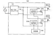
以下、本発明の一実施例であるLEDストロボ点灯電源装置について、添付図面を参照して説明する。図1は本実施例のLEDストロボ点灯電源装置のブロック構成図、図2は図1中の定電圧回路のブロック構成図である。 An LED strobe lighting power supply device according to an embodiment of the present invention will be described below with reference to the accompanying drawings. FIG. 1 is a block configuration diagram of an LED strobe lighting power supply device of this embodiment, and FIG. 2 is a block configuration diagram of a constant voltage circuit in FIG.
図1において、AC/DCコンバータ10、第1、第2であるバルス発生部14a、14b、第1、第2である半導体スイッチ15a、15b、及び制御部16はそれぞれ、図4に示した従来装置におけるAC/DCコンバータ101、バルス発生部103a、103b、半導体スイッチ104a、104b、及び制御部105、と同じである。
In FIG. 1, the AC /
本実施例のLEDストロボ点灯電源装置1では、第1半導体スイッチ15aに対応して第1定電圧回路13aが設けられ、第2半導体スイッチ15bに対応して第2定電圧回路13bが設けられている。第1、第2定電圧回路13a、13bそれぞれの正負電圧入力端間には、図4に示した従来装置におけるコンデンサ102と同様の機能を有する第1、第2コンデンサ12a、12bが接続されている。そして、AC/DCコンバータ10の正電圧出力端と第1、第2定電圧回路13a、13bの正電圧入力端の間にはそれぞれ第1、第2抵抗器11a、11bが接続されている。即ち、AC/DCコンバータ10の正負電圧出力端から負荷側を見たとき、第1抵抗器11a、第1コンデンサ12a、第1定電圧回路13a、第1パルス発生部14a、及び第1半導体スイッチ15aを含む第1のLED駆動部と、第2抵抗器11b、第2コンデンサ12b、第2定電圧回路13b、第2パルス発生部14b、及び第2半導体スイッチ15bを含む第2のLED駆動部と、が並列に接続された構成となっている。ここで、抵抗器11a、11bは例えば数Ω程度の小さな抵抗値を有するものである。
In the LED strobe lighting
図2に示すように、第1、第2定電圧回路13a、13bは電圧降下を利用した一般的な回路であり、トランジスタなどを含む定電圧駆動部131と、定電圧制御部132と、電圧検出部133と、を含む。電圧検出部133は定電圧回路13a、13bの出力電圧を検出してその検出値を定電圧制御部132にフィードバックする。定電圧制御部132はツェナーダイオードなどによる基準電圧回路を含み、検出電圧が基準電圧になるように例えば定電圧駆動部131に含まれるトランジスタのベース電流を制御する。本実施例のLEDストロボ点灯電源装置1では一例として、定電圧回路13a、13bは入力電圧が標準的に48[V]、出力電圧が36[V]であるものとしている。
As shown in FIG. 2, the first and second
本実施例のLEDストロボ点灯電源装置1の動作を説明する。図3は点灯動作の際の波形図である。
AC/DCコンバータ10は外部の商用交流電源2から供給される交流電力を直流電力に変換する。AC/DCコンバータ10の正電圧出力端から出力される直流電圧(本発明における第1の直流電圧)は標準的に48[V]である。この電圧は第1、第2抵抗器11a、11bを通して第1、第2定電圧回路13a、13bの正電圧入力端にそれぞれ入力される。また、この電圧により第1、第2コンデンサ12a、12bはそれぞれ充電される。第1、第2定電圧回路13a、13bは、入力された48Vの直流電圧を36V一定の直流電圧(本発明における第2の直流電圧)としてそれぞれ出力する。これにより、第1、第2半導体スイッチ15a、15bがいずれもオフであるとき、第1、第2定電圧回路13a、13bの出力端には約36[V]の直流電圧が出力されている。
The operation of the LED strobe lighting
The AC /
Ch.1のLED3aをストロボ点灯させるとき、制御部16の指示を受けた第1パルス発生部14aは設定された発光時間に応じた10〜1000[μsec]程度の幅のパルス信号を生成し第1半導体スイッチ15aのゲート端子に加える。第1半導体スイッチ15aはパルス信号がHレベルである期間だけオンする。すると、第1半導体スイッチ15aを介して第1定電圧回路13aの正負電圧出力端間にLED3aが接続されるから、第1定電圧回路13aの出力電圧に応じた駆動電流がLED3aに流れ、該LED3aは発光する。
Ch. When the
半導体スイッチ15aがオンして第1定電圧回路13aからLED3aに駆動電流が流れるとき、該電流を生成するためにAC/DCコンバータ10から第1定電圧回路13aへ電流が流れるため、AC/DCコンバータ10の出力電圧は下がろうとする。このとき、第1定電圧回路13aの電圧入力端に設けられた第1コンデンサ12aに蓄えられた電気エネルギーにより第1定電圧回路13aに電流が供給されるため、該定電圧回路13aの入力電圧の急な電圧低下は抑えられる。もちろん、AC/DCコンバータ10のもともとの出力電圧は48[V]であり、定電圧回路13aの入力電圧、出力電圧の差は十分に大きくなっているため、仮にAC/DCコンバータ10の出力電圧が下がったとしても定電圧回路13aの定電圧動作が機能しなくなるほど入力電圧が下がることはない。そのため、第1定電圧回路13aの出力電圧は一定に維持され、図3中に示すようにLED3aに電圧値が一定であるパルス状の駆動電圧を印加することができる。
When the
Ch.2のLED3bをストロボ点灯させる場合の動作も全く同じであり、図3中に示すようにLED3bに電圧値が一定であるパルス状の駆動電圧を印加することができる。
Ch. The operation when the
先に説明した図6(b)、(c)に示したように、Ch.1のLED3aとCh.2のLED3bを同時に又は少なくともその発光期間の一部が重なるようにストロボ点灯させるとき、本発明に係る図1に示した本実施例の装置では、第1、第2定電圧回路13a、13は独立に動作し、それぞれ一定の直流電圧を出力する。二つの定電圧回路13a、13bは第1、第2抵抗器11a、11bを介して接続されているので、例えば第1定電圧回路13aの正電圧入力端で電圧が低下したとしても、その電圧低下の影響は第2定電圧回路13bの正電圧入力端に殆ど現れない。そのため、各定電圧回路13a、13から同時に駆動電流が流れた場合でも、各定電圧回路13a、13の正電圧入力端における電圧低下の状態は、図3に示したように一つのLED3a又は3bが点灯した場合と殆ど同じである。したがって、各定電圧回路13a、13bへの入力電圧はそれら定電圧回路13a、13bによる定電圧動作に影響を及ぼさないレベル以上を維持し、この場合にも、定電圧回路13a、13bの出力電圧は36Vを維持しそれ以下には低下しない。したがって、各LED3a、3bに電圧値が一定であるパルス状の駆動電圧をそれぞれ印加することができる。
As shown in FIGS. 6B and 6C described above, the Ch. 1
また、LED3a、3bが発光する際に第1、第2コンデンサ12a、12bから第1、第2定電圧回路13a、13bに電流が流れるため、そのあと、それらコンデンサ12a、12bをそれぞれ充電するためにAC/DCコンバータ10から充電電流が流れる。仮に抵抗器11a、11bがないとすると、第1、第2半導体スイッチ15a、15bがオフされた直後にAC/DCコンバータ10から急に大きな充電電流が流れることになり、これを賄うような出力容量が必要となる。これに対し本実施例のLEDストロボ点灯電源装置1では、AC/DCコンバータ10の電圧出力端とコンデンサ12a、12bとの間に抵抗器11a、11bがあり、この抵抗器11a、11bのために充電電流が制限される。その結果、コンデンサ12a、12bの充電には或る程度の時間が掛かるものの、AC/DCコンバータ10の出力容量をそれほど大きくする必要はなく、比較的低コストのスイッチング電源を用いることができる。
Further, when the
ここで、上記動作の際の具体的な数値例を示す。いま、LED照明器具を駆動する出力の仕様が、出力電流:5[A]、出力電圧:36[V]、最大点灯時間:1[msec]、であるとする。この場合、LED3a(又は3b)を1回発光させるときの発光エネルギーは、
5×36×0.001[sec]=0.18[J}
である。コンデンサ12a(又は12b)の容量が1000[μF]であるとすると、該コンデンサ12a(又は12b)の充電電圧は48[V]であるから、コンデンサ12a(又は12b)に蓄えられるエネルギーは、
(1/2)CV2=(1/2)・1×10-3[F]・482=1.152[J]
である。LED3a(又は3b)が1回発光して電圧が低下したときのコンデンサ12a(又は12b)の両端電圧つまりは定電圧回路13a(又は13b)の入力電圧をVLとすると、
(1/2)CV2−(1/2)CVL 2=0.18[J]
これを解くと、VL=44.09[V]である。即ち、1チャンネルのLED照明器具がストロボ点灯すると、定電圧回路13a、13bの入力電圧は4[V]程度低下することになる。
Here, a specific numerical example of the above operation will be shown. Now, it is assumed that the specifications of the output for driving the LED lighting device are output current: 5 [A], output voltage: 36 [V], and maximum lighting time: 1 [msec]. In this case, the emission energy when the
5 x 36 x 0.001 [sec] = 0.18 [J}
Is. If the capacity of the
(1/2) CV 2 = (1/2) ・ 1 × 10 -3 [F] ・ 48 2 = 1.152 [J]
Is. If the voltage across the
(1/2) CV 2 - (1/2 )
Solving this, V L = 44.09 [V]. That is, when the 1-channel LED lighting fixture is strobe-lighted, the input voltage of the
上述したように、AC/DCコンバータ10の電圧出力端と定電圧回路13a、13bの電圧入力端との間にはそれぞれ抵抗器11a、11bがあるため、二つのLED3a、3bが同時に又は発光期間の一部が重なるように発光したときでも、一方の定電圧回路の正電圧入力端の電圧低下は他方の定電圧回路の正電圧入力端の電圧に殆ど影響を及ぼさない。そのため、二つのLED3a、3bが同時に又は発光期間の一部が重なるように発光した場合にも、各定電圧回路13a、13bの正電圧入力端の電圧は44[V]程度以上である。一般に定電圧回路13a、13bでは正常な定電圧動作のために出力電圧よりも3[V]程度以上高い電圧を入力する必要があるが、上述したように入力電圧が44[V]まで下がったとしても、出力電圧(36[V])よりも3[V]だけ高い39[V]以上を十分な余裕を以て確保することができる。したがって、定電圧回路13a、13bから一定の電圧を出力することができ、LED3a、3bの発光光量の変動を回避することができる。
もちろん、ここで示した電圧値やコンデンサの容量値などの数値は単に一例であり、適宜に変更できることは当然である。
As described above, since the
Of course, the numerical values such as the voltage value and the capacitance value of the capacitor shown here are merely examples, and it goes without saying that they can be appropriately changed.
以上のように本実施例のLEDストロボ点灯電源装置では、単一のLED照明器具が点灯される場合はもちろんのこと、複数のLED照明器具が同時に又は発光期間の一部が重なるようにストロボ点灯される場合でも、各LED照明器具に対し電圧値が一定のパルス状の駆動電圧を印加することができる。それにより、各LED照明器具の発光光量のばらつきや時間変動をなくすことができる。 As described above, in the LED strobe lighting power supply device according to the present embodiment, not only when a single LED lighting fixture is turned on, but also when a plurality of LED lighting fixtures are turned on at the same time or so that part of the light emitting period overlaps. Even in such a case, a pulsed drive voltage having a constant voltage value can be applied to each LED lighting fixture. As a result, it is possible to eliminate variations in the amount of light emitted from the LED lighting devices and time variations.
なお、上記実施例は本発明の一例にすぎず、本発明の趣旨の範囲で適宜変形や修正、追加を加えても本願特許請求の範囲に包含されることは明らかである。 It should be noted that the above embodiment is merely an example of the present invention, and it is obvious that appropriate modifications, corrections, and additions are included in the scope of the claims of the present invention within the scope of the spirit of the present invention.
1…LEDストロボ点灯電源装置
10…AC/DCコンバータ
11a、11b…抵抗器
12a、12b…コンデンサ
13a、13b…定電圧回路
14a、14b…バルス発生部
15a、15b…半導体スイッチ
16…制御部
2…商用交流電源
3a、3b…LED
1 ... LED strobe lighting
Claims (1)
a)前記複数のLED照明器具にそれぞれ対応して設けられ、各LED照明器具に供給する駆動電流をオン・オフする複数の半導体スイッチと、
b)商用交流電源による交流電圧を第1の直流電圧に変換する交流−直流変換回路と、
c)前記複数の半導体スイッチを通して前記複数のLED照明器具にそれぞれ駆動電流を供給するために該複数の半導体スイッチにそれぞれ対応して設けられ、前記交流−直流変換回路の出力電圧を受けて前記第1の直流電圧よりも低い電圧値である第2の直流電圧を出力する複数の定電圧回路と、
d)前記複数の定電圧回路のそれぞれにおいて正負の電圧入力端間に接続された電圧低下抑制用の複数のコンデンサと、
e)前記交流−直流変換回路の正電圧出力端と前記複数の定電圧回路の正電圧入力端との間にそれぞれ介挿された複数の抵抗器と、
を備え、前記第1の直流電圧の電圧値と前記第2の直流電圧の電圧値の差を前記複数のLED照明器具が同時にストロボ点灯したときの前記交流−直流変換回路の出力電圧の低下よりも大きく定めたことを特徴とするLEDストロボ点灯電源装置。 In LED strobe lighting power supply for flash lights with independent timing multiple LED lighting fixture,
a) a plurality of semiconductor switches that are provided corresponding to the plurality of LED lighting fixtures and that turn on / off a drive current supplied to each LED lighting fixture,
b) an AC-DC conversion circuit that converts an AC voltage from a commercial AC power supply into a first DC voltage,
c) is provided corresponding to each of the plurality of semiconductor switches for supplying a driving current to each of the plurality of LED lighting fixtures through the plurality of semiconductor switches, and receives the output voltage of the AC-DC conversion circuit to receive the output voltage. A plurality of constant voltage circuits that output a second DC voltage that is a voltage value lower than the DC voltage of 1;
d) a plurality of capacitors for suppressing a voltage drop connected between positive and negative voltage input terminals in each of the plurality of constant voltage circuits,
e) a plurality of resistors respectively inserted between the positive voltage output terminal of the AC-DC conversion circuit and the positive voltage input terminals of the plurality of constant voltage circuits,
The difference between the voltage value of the first DC voltage and the voltage value of the second DC voltage from the decrease of the output voltage of the AC-DC conversion circuit when the plurality of LED lighting fixtures are simultaneously strobe lighting. LED strobe lighting power supply device characterized in that
Priority Applications (1)
| Application Number | Priority Date | Filing Date | Title |
|---|---|---|---|
| JP2016113585A JP6697188B2 (en) | 2016-06-07 | 2016-06-07 | LED strobe lighting power supply |
Applications Claiming Priority (1)
| Application Number | Priority Date | Filing Date | Title |
|---|---|---|---|
| JP2016113585A JP6697188B2 (en) | 2016-06-07 | 2016-06-07 | LED strobe lighting power supply |
Publications (3)
| Publication Number | Publication Date |
|---|---|
| JP2017220349A JP2017220349A (en) | 2017-12-14 |
| JP2017220349A5 JP2017220349A5 (en) | 2019-05-23 |
| JP6697188B2 true JP6697188B2 (en) | 2020-05-20 |
Family
ID=60656292
Family Applications (1)
| Application Number | Title | Priority Date | Filing Date |
|---|---|---|---|
| JP2016113585A Active JP6697188B2 (en) | 2016-06-07 | 2016-06-07 | LED strobe lighting power supply |
Country Status (1)
| Country | Link |
|---|---|
| JP (1) | JP6697188B2 (en) |
-
2016
- 2016-06-07 JP JP2016113585A patent/JP6697188B2/en active Active
Also Published As
| Publication number | Publication date |
|---|---|
| JP2017220349A (en) | 2017-12-14 |
Similar Documents
| Publication | Publication Date | Title |
|---|---|---|
| US8581512B2 (en) | Light source module, lighting apparatus, and illumination device using the same | |
| KR102062566B1 (en) | Led emitting device and driving method thereof | |
| KR102085725B1 (en) | Led lighting system of ac direct type and control method thereof | |
| JP2011119738A (en) | Light-emitting apparatus | |
| KR20130120407A (en) | Light emitting diode dimming apparatus | |
| EP2602301B1 (en) | Organic el element lighting device and lighting fixture using the same | |
| US9167654B2 (en) | Solid light source lighting device, illumination apparatus, and illumination system | |
| US20170150568A1 (en) | Light-dimming device | |
| TWI583120B (en) | A system and method for providing an output current to one or more light emitting diodes | |
| JP6153024B2 (en) | LIGHT EMITTING ELEMENT LIGHTING DEVICE, LIGHT EMITTING MODULE, LIGHTING DEVICE, AND LIGHT EMITTING ELEMENT LIGHTING METHOD | |
| KR101536108B1 (en) | Control circuit and voltage generating method for led lighting apparatus | |
| JP7017433B2 (en) | LED strobe | |
| US9888532B2 (en) | Lighting circuit and illumination system | |
| JP2010153566A (en) | Led driving method | |
| US8786214B2 (en) | Light emitting element drive device and lighting device | |
| JP2016201276A (en) | Lighting circuit, lighting fixture, and illumination system | |
| JP6697188B2 (en) | LED strobe lighting power supply | |
| US10231298B2 (en) | Integrated light emitting diode driving circuit | |
| JP2016058240A (en) | Light emission element lighting device, light emission module and luminaire | |
| JP6358526B2 (en) | Lighting device and lighting apparatus using the same | |
| JP6257485B2 (en) | LED lighting device | |
| JP2018037233A (en) | Led lighting device and led illumination device | |
| JP2011244619A (en) | Switching power supply | |
| TW201630466A (en) | Driving device | |
| JP2016126825A (en) | Switching power supply circuit |
Legal Events
| Date | Code | Title | Description |
|---|---|---|---|
| A521 | Request for written amendment filed |
Free format text: JAPANESE INTERMEDIATE CODE: A523 Effective date: 20190402 |
|
| A621 | Written request for application examination |
Free format text: JAPANESE INTERMEDIATE CODE: A621 Effective date: 20190402 |
|
| A977 | Report on retrieval |
Free format text: JAPANESE INTERMEDIATE CODE: A971007 Effective date: 20200207 |
|
| TRDD | Decision of grant or rejection written | ||
| A01 | Written decision to grant a patent or to grant a registration (utility model) |
Free format text: JAPANESE INTERMEDIATE CODE: A01 Effective date: 20200310 |
|
| A61 | First payment of annual fees (during grant procedure) |
Free format text: JAPANESE INTERMEDIATE CODE: A61 Effective date: 20200408 |
|
| R150 | Certificate of patent or registration of utility model |
Ref document number: 6697188 Country of ref document: JP Free format text: JAPANESE INTERMEDIATE CODE: R150 |
|
| R250 | Receipt of annual fees |
Free format text: JAPANESE INTERMEDIATE CODE: R250 |