JP6681581B2 - Light emitting device and lighting device - Google Patents
Light emitting device and lighting device Download PDFInfo
- Publication number
- JP6681581B2 JP6681581B2 JP2015249057A JP2015249057A JP6681581B2 JP 6681581 B2 JP6681581 B2 JP 6681581B2 JP 2015249057 A JP2015249057 A JP 2015249057A JP 2015249057 A JP2015249057 A JP 2015249057A JP 6681581 B2 JP6681581 B2 JP 6681581B2
- Authority
- JP
- Japan
- Prior art keywords
- light emitting
- light
- emitting device
- phosphor
- emitting element
- Prior art date
- Legal status (The legal status is an assumption and is not a legal conclusion. Google has not performed a legal analysis and makes no representation as to the accuracy of the status listed.)
- Active
Links
Images


Classifications
-
- F—MECHANICAL ENGINEERING; LIGHTING; HEATING; WEAPONS; BLASTING
- F21—LIGHTING
- F21K—NON-ELECTRIC LIGHT SOURCES USING LUMINESCENCE; LIGHT SOURCES USING ELECTROCHEMILUMINESCENCE; LIGHT SOURCES USING CHARGES OF COMBUSTIBLE MATERIAL; LIGHT SOURCES USING SEMICONDUCTOR DEVICES AS LIGHT-GENERATING ELEMENTS; LIGHT SOURCES NOT OTHERWISE PROVIDED FOR
- F21K9/00—Light sources using semiconductor devices as light-generating elements, e.g. using light-emitting diodes [LED] or lasers
- F21K9/60—Optical arrangements integrated in the light source, e.g. for improving the colour rendering index or the light extraction
- F21K9/64—Optical arrangements integrated in the light source, e.g. for improving the colour rendering index or the light extraction using wavelength conversion means distinct or spaced from the light-generating element, e.g. a remote phosphor layer
-
- F—MECHANICAL ENGINEERING; LIGHTING; HEATING; WEAPONS; BLASTING
- F21—LIGHTING
- F21V—FUNCTIONAL FEATURES OR DETAILS OF LIGHTING DEVICES OR SYSTEMS THEREOF; STRUCTURAL COMBINATIONS OF LIGHTING DEVICES WITH OTHER ARTICLES, NOT OTHERWISE PROVIDED FOR
- F21V19/00—Fastening of light sources or lamp holders
- F21V19/001—Fastening of light sources or lamp holders the light sources being semiconductors devices, e.g. LEDs
- F21V19/003—Fastening of light source holders, e.g. of circuit boards or substrates holding light sources
-
- F—MECHANICAL ENGINEERING; LIGHTING; HEATING; WEAPONS; BLASTING
- F21—LIGHTING
- F21V—FUNCTIONAL FEATURES OR DETAILS OF LIGHTING DEVICES OR SYSTEMS THEREOF; STRUCTURAL COMBINATIONS OF LIGHTING DEVICES WITH OTHER ARTICLES, NOT OTHERWISE PROVIDED FOR
- F21V23/00—Arrangement of electric circuit elements in or on lighting devices
- F21V23/001—Arrangement of electric circuit elements in or on lighting devices the elements being electrical wires or cables
- F21V23/002—Arrangements of cables or conductors inside a lighting device, e.g. means for guiding along parts of the housing or in a pivoting arm
-
- F—MECHANICAL ENGINEERING; LIGHTING; HEATING; WEAPONS; BLASTING
- F21—LIGHTING
- F21V—FUNCTIONAL FEATURES OR DETAILS OF LIGHTING DEVICES OR SYSTEMS THEREOF; STRUCTURAL COMBINATIONS OF LIGHTING DEVICES WITH OTHER ARTICLES, NOT OTHERWISE PROVIDED FOR
- F21V7/00—Reflectors for light sources
- F21V7/04—Optical design
- F21V7/041—Optical design with conical or pyramidal surface
-
- F—MECHANICAL ENGINEERING; LIGHTING; HEATING; WEAPONS; BLASTING
- F21—LIGHTING
- F21V—FUNCTIONAL FEATURES OR DETAILS OF LIGHTING DEVICES OR SYSTEMS THEREOF; STRUCTURAL COMBINATIONS OF LIGHTING DEVICES WITH OTHER ARTICLES, NOT OTHERWISE PROVIDED FOR
- F21V9/00—Elements for modifying spectral properties, polarisation or intensity of the light emitted, e.g. filters
- F21V9/30—Elements containing photoluminescent material distinct from or spaced from the light source
-
- H—ELECTRICITY
- H01—ELECTRIC ELEMENTS
- H01L—SEMICONDUCTOR DEVICES NOT COVERED BY CLASS H10
- H01L25/00—Assemblies consisting of a plurality of individual semiconductor or other solid state devices ; Multistep manufacturing processes thereof
- H01L25/03—Assemblies consisting of a plurality of individual semiconductor or other solid state devices ; Multistep manufacturing processes thereof all the devices being of a type provided for in the same subgroup of groups H01L27/00 - H01L33/00, or in a single subclass of H10K, H10N, e.g. assemblies of rectifier diodes
- H01L25/04—Assemblies consisting of a plurality of individual semiconductor or other solid state devices ; Multistep manufacturing processes thereof all the devices being of a type provided for in the same subgroup of groups H01L27/00 - H01L33/00, or in a single subclass of H10K, H10N, e.g. assemblies of rectifier diodes the devices not having separate containers
- H01L25/075—Assemblies consisting of a plurality of individual semiconductor or other solid state devices ; Multistep manufacturing processes thereof all the devices being of a type provided for in the same subgroup of groups H01L27/00 - H01L33/00, or in a single subclass of H10K, H10N, e.g. assemblies of rectifier diodes the devices not having separate containers the devices being of a type provided for in group H01L33/00
- H01L25/0753—Assemblies consisting of a plurality of individual semiconductor or other solid state devices ; Multistep manufacturing processes thereof all the devices being of a type provided for in the same subgroup of groups H01L27/00 - H01L33/00, or in a single subclass of H10K, H10N, e.g. assemblies of rectifier diodes the devices not having separate containers the devices being of a type provided for in group H01L33/00 the devices being arranged next to each other
-
- F—MECHANICAL ENGINEERING; LIGHTING; HEATING; WEAPONS; BLASTING
- F21—LIGHTING
- F21Y—INDEXING SCHEME ASSOCIATED WITH SUBCLASSES F21K, F21L, F21S and F21V, RELATING TO THE FORM OR THE KIND OF THE LIGHT SOURCES OR OF THE COLOUR OF THE LIGHT EMITTED
- F21Y2113/00—Combination of light sources
- F21Y2113/10—Combination of light sources of different colours
- F21Y2113/13—Combination of light sources of different colours comprising an assembly of point-like light sources
- F21Y2113/17—Combination of light sources of different colours comprising an assembly of point-like light sources forming a single encapsulated light source
-
- F—MECHANICAL ENGINEERING; LIGHTING; HEATING; WEAPONS; BLASTING
- F21—LIGHTING
- F21Y—INDEXING SCHEME ASSOCIATED WITH SUBCLASSES F21K, F21L, F21S and F21V, RELATING TO THE FORM OR THE KIND OF THE LIGHT SOURCES OR OF THE COLOUR OF THE LIGHT EMITTED
- F21Y2115/00—Light-generating elements of semiconductor light sources
- F21Y2115/10—Light-emitting diodes [LED]
-
- H—ELECTRICITY
- H01—ELECTRIC ELEMENTS
- H01L—SEMICONDUCTOR DEVICES NOT COVERED BY CLASS H10
- H01L2224/00—Indexing scheme for arrangements for connecting or disconnecting semiconductor or solid-state bodies and methods related thereto as covered by H01L24/00
- H01L2224/01—Means for bonding being attached to, or being formed on, the surface to be connected, e.g. chip-to-package, die-attach, "first-level" interconnects; Manufacturing methods related thereto
- H01L2224/42—Wire connectors; Manufacturing methods related thereto
- H01L2224/47—Structure, shape, material or disposition of the wire connectors after the connecting process
- H01L2224/48—Structure, shape, material or disposition of the wire connectors after the connecting process of an individual wire connector
- H01L2224/481—Disposition
- H01L2224/48135—Connecting between different semiconductor or solid-state bodies, i.e. chip-to-chip
- H01L2224/48137—Connecting between different semiconductor or solid-state bodies, i.e. chip-to-chip the bodies being arranged next to each other, e.g. on a common substrate
-
- H—ELECTRICITY
- H01—ELECTRIC ELEMENTS
- H01L—SEMICONDUCTOR DEVICES NOT COVERED BY CLASS H10
- H01L2924/00—Indexing scheme for arrangements or methods for connecting or disconnecting semiconductor or solid-state bodies as covered by H01L24/00
- H01L2924/15—Details of package parts other than the semiconductor or other solid state devices to be connected
- H01L2924/181—Encapsulation
-
- H—ELECTRICITY
- H01—ELECTRIC ELEMENTS
- H01L—SEMICONDUCTOR DEVICES NOT COVERED BY CLASS H10
- H01L33/00—Semiconductor devices with at least one potential-jump barrier or surface barrier specially adapted for light emission; Processes or apparatus specially adapted for the manufacture or treatment thereof or of parts thereof; Details thereof
- H01L33/48—Semiconductor devices with at least one potential-jump barrier or surface barrier specially adapted for light emission; Processes or apparatus specially adapted for the manufacture or treatment thereof or of parts thereof; Details thereof characterised by the semiconductor body packages
- H01L33/50—Wavelength conversion elements
- H01L33/501—Wavelength conversion elements characterised by the materials, e.g. binder
- H01L33/502—Wavelength conversion materials
- H01L33/504—Elements with two or more wavelength conversion materials
Description
本発明は、発光装置、及び、発光装置を用いた照明装置に関する。 The present invention relates to a light emitting device and a lighting device using the light emitting device.
発光ダイオード(LED:Light Emitting Diode)等の半導体発光素子は、高効率で省スペースな光源として照明用途またはディスプレイ用途等の各種の照明装置に広く利用されている。 A semiconductor light emitting element such as a light emitting diode (LED) is widely used as a highly efficient and space-saving light source for various lighting devices such as lighting applications and display applications.
また、基板に実装されたLEDを透光性の樹脂で封止したCOB(Chip On Board)型のLED光源が知られている(例えば、特許文献1参照)。 In addition, a COB (Chip On Board) type LED light source in which an LED mounted on a substrate is sealed with a translucent resin is known (see, for example, Patent Document 1).
LEDなどの発光素子を用いた発光装置が発する白色光は、発光スペクトルに偏りがあるため、自然光よりも色の再現性が低い。つまり、発光装置においては、色の再現性を向上することが課題となる。 White light emitted by a light-emitting device using a light-emitting element such as an LED has uneven emission spectrum and thus has lower color reproducibility than natural light. That is, in the light emitting device, improving color reproducibility is a problem.
本発明は、赤色の再現性を向上することができる発光装置及び照明装置を提供する。 The present invention provides a light emitting device and a lighting device capable of improving red color reproducibility.
本発明の一態様に係る発光装置は、発光ピーク波長が430nm以上470nm以下の第一発光素子と、発光ピーク波長が600nm以上640nm以下の第二発光素子と、前記第一発光素子が発する光で励起されて発光ピーク波長が500nm以上580nm以下の光を発する第一蛍光体と、前記第一発光素子が発する光で励起されて発光ピーク波長が640nm以上670nm以下の光を発する第二蛍光体とを備え、前記第一発光素子、前記第二発光素子、前記第一蛍光体、及び、前記第二蛍光体のそれぞれが発する光が混ざることにより白色光を発する。 A light-emitting device according to one embodiment of the present invention includes a first light-emitting element having a light-emission peak wavelength of 430 nm to 470 nm, a second light-emitting element having a light-emission peak wavelength of 600 nm to 640 nm, and light emitted from the first light-emitting element. A first phosphor that emits light having an emission peak wavelength of 500 nm or more and 580 nm or less when excited, and a second phosphor that emits light having an emission peak wavelength of 640 nm or more and 670 nm or less when excited by the light emitted by the first light emitting element. In addition, white light is emitted by mixing lights emitted from each of the first light emitting element, the second light emitting element, the first phosphor, and the second phosphor.
本発明の一態様に係る照明装置は、上記いずれかの態様の発光装置と、前記発光装置に、当該発光装置を点灯させるための電力を供給する点灯装置とを備える。 An illumination device according to one aspect of the present invention includes the light emitting device according to any one of the above aspects, and a lighting device that supplies power to the light emitting device to light the light emitting device.
本発明の一態様に係る発光装置及び照明装置は、赤色の再現性を向上することができる。 The light emitting device and the lighting device according to one embodiment of the present invention can improve red color reproducibility.
以下、実施の形態に係る発光装置等について、図面を参照しながら説明する。なお、以下で説明する実施の形態は、いずれも包括的または具体的な例を示すものである。以下の実施の形態で示される数値、形状、材料、構成要素、構成要素の配置位置及び接続形態、ステップ、ステップの順序などは、一例であり、本発明を限定する主旨ではない。また、以下の実施の形態における構成要素のうち、最上位概念を示す独立請求項に記載されていない構成要素については、任意の構成要素として説明される。 Hereinafter, a light emitting device and the like according to embodiments will be described with reference to the drawings. It should be noted that each of the embodiments described below shows a comprehensive or specific example. Numerical values, shapes, materials, constituent elements, arrangement positions and connection forms of constituent elements, steps, order of steps, and the like shown in the following embodiments are examples, and are not intended to limit the present invention. Further, among the constituent elements in the following embodiments, constituent elements that are not described in the independent claims showing the highest concept are described as arbitrary constituent elements.
なお、各図は模式図であり、必ずしも厳密に図示されたものではない。また、各図において、実質的に同一の構成に対しては同一の符号を付しており、重複する説明は省略または簡略化される場合がある。 It should be noted that each drawing is a schematic view and is not necessarily strictly illustrated. Further, in each drawing, substantially the same configurations are denoted by the same reference numerals, and overlapping description may be omitted or simplified.
また、以下の実施の形態において、Z軸方向は、例えば鉛直方向であり、Z軸+側は、上側(上方)と記載される場合がある。また、Z軸−側は、下側(下方)と記載される場合がある。また、X軸方向及びY軸方向は、Z軸に垂直な平面(水平面)上において、互いに直交する方向である。 In the following embodiments, the Z-axis direction is, for example, the vertical direction, and the Z-axis + side may be described as the upper side (upper side). Further, the Z-axis-side may be described as the lower side (lower side). The X-axis direction and the Y-axis direction are directions orthogonal to each other on a plane (horizontal plane) perpendicular to the Z-axis.
(実施の形態1)
[発光装置の構成]
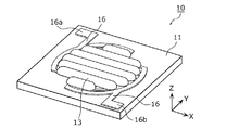
まず、実施の形態1に係る発光装置の構成について図面を用いて説明する。図1は、実施の形態1に係る発光装置の外観斜視図である。図2は、実施の形態1に係る発光装置の平面図である。図3は、実施の形態1に係る発光装置の内部構造を示す平面図である。図4は、図2のIV−IV線における模式断面図である。なお、上記の図3は、図2において封止部材13を取り除き、LEDチップの配列及び配線パターンなどの内部の構造を示した平面図である。
(Embodiment 1)
[Configuration of light emitting device]
First, the configuration of the light emitting device according to the first embodiment will be described with reference to the drawings. FIG. 1 is an external perspective view of the light emitting device according to the first embodiment. FIG. 2 is a plan view of the light emitting device according to the first embodiment. FIG. 3 is a plan view showing the internal structure of the light emitting device according to the first embodiment. FIG. 4 is a schematic cross-sectional view taken along the line IV-IV in FIG. It should be noted that FIG. 3 is a plan view showing an internal structure such as an arrangement of LED chips and a wiring pattern with the sealing
図1〜図4に示されるように、実施の形態1に係る発光装置10は、基板11と、複数の青色LEDチップ12bと、複数の赤色LEDチップ12rと、封止部材13とを備える。以下では、青色LEDチップ12b及び赤色LEDチップ12rの総称として単に「LEDチップ」と記載される場合がある。
As shown in FIGS. 1 to 4, the
発光装置10は、基板11に青色LEDチップ12b及び赤色LEDチップ12rが直接実装された、いわゆるCOB構造のLEDモジュールである。
The
基板11は、青色LEDチップ12b及び赤色LEDチップ12rに電力を供給するための配線16が設けられた配線領域を有する基板である。配線16(並びに、電極16a及び電極16b)は、金属により形成される。基板11は、例えば、メタルベース基板またはセラミック基板である。また、基板11は、樹脂を基材とする樹脂基板であってもよい。
The
セラミック基板としては、酸化アルミニウム(アルミナ)からなるアルミナ基板または窒化アルミニウムからなる窒化アルミニウム基板等が採用される。また、メタルベース基板としては、例えば、表面に絶縁膜が形成された、アルミニウム合金基板、鉄合金基板または銅合金基板等が採用される。樹脂基板としては、例えば、ガラス繊維とエポキシ樹脂とからなるガラスエポキシ基板等が採用される。 As the ceramic substrate, an alumina substrate made of aluminum oxide (alumina) or an aluminum nitride substrate made of aluminum nitride is used. Further, as the metal base substrate, for example, an aluminum alloy substrate, an iron alloy substrate, a copper alloy substrate, or the like having an insulating film formed on the surface is adopted. As the resin substrate, for example, a glass epoxy substrate made of glass fiber and epoxy resin is used.
なお、基板11として、光反射率が高い(例えば、光反射率が90%以上の)基板が採用されてもよい。基板11として光反射率の高い基板が採用されることで、青色LEDチップ12b及び赤色LEDチップ12rが発する光を基板11の表面で反射させることができる。この結果、発光装置10の光取り出し効率が向上される。このような基板としては、例えばアルミナを基材とする白色セラミック基板が例示される。
A substrate having a high light reflectance (for example, a light reflectance of 90% or more) may be used as the
また、基板11として、光の透過率が高い透光性基板が採用されてもよい。このような基板としては、多結晶のアルミナや窒化アルミニウムからなる透光性セラミックス基板、ガラスからなる透明ガラス基板、水晶からなる水晶基板、サファイアからなるサファイア基板または透明樹脂材料からなる透明樹脂基板が例示される。
Further, as the
なお、実施の形態1では基板11は矩形であるが、円形などその他の形状であってもよい。
Although the
青色LEDチップ12bは、第一発光素子の一例であって、青色光を発するLEDチップである。青色LEDチップ12bは、例えば、InGaN系の材料によって形成される。青色LEDチップ12bの発光ピーク波長は、例えば、430nm以上470nm以下である。
The
赤色LEDチップ12rは、第二発光素子の一例であって、赤色光を発するLEDチップである。赤色LEDチップ12rは、例えば、AlGaInP系の材料によって形成される。赤色LEDチップ12rの発光ピーク波長は、例えば、600nm以上640nm以下である。
The
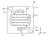
基板11上には、複数のLEDチップからなる発光素子列が複数設けられている。図3に示されるように、構造的には、X軸方向に沿う発光素子列が7列、基板11上に設けられている。
A plurality of light emitting element rows each including a plurality of LED chips are provided on the
電気的には、12個の直列接続されたLEDチップからなる発光素子列が5列、基板11上に設けられている。これら5列の発光素子列は並列接続され、電極16aと電極16bとの間に電力が供給されることにより発光する。
Electrically, five rows of light emitting elements each including 12 LED chips connected in series are provided on the
また、これら5列の発光素子列のうち、一の発光素子列は、青色LEDチップ12b、及び、赤色LEDチップ12rを少なくとも一つずつ含む。つまり、一の発光素子列においては、青色LEDチップ12b、及び、赤色LEDチップ12rが直列接続されている。そして、一の発光素子列は、他の発光素子列と同じ数の青色LEDチップ12b、及び、他の発光素子列と同じ数の赤色LEDチップ12rを含む。これにより、複数の発光素子列のそれぞれにおける、LEDチップのトータルVfを揃えることができ、発光装置を点灯させるための点灯装置の構成を簡素化できる。
Further, among the five light emitting element rows, one light emitting element row includes at least one
図3の例では、一の発光素子列に含まれる青色LEDチップ12bの数は、8個であり、一の発光素子列に含まれる赤色LEDチップ12rの数は、4個である。つまり、一の発光素子列に含まれる青色LEDチップ12bの数は、当該一の発光素子列に含まれる赤色LEDチップ12rの数の2倍である。
In the example of FIG. 3, the number of
また、一の赤色LEDチップ12rは、X軸方向及びY軸方向のいずれの方向においても他の赤色LEDチップ12rと隣接しないように分散配置されている。これにより、発光装置10は、赤味が均一な白色光を発することができる。
Further, the one
また、直列接続されたLEDチップ同士は、主に、ボンディングワイヤ17によってChip To Chipで接続される(一部のLEDチップ12については、配線16によって接続される)。ボンディングワイヤ17は、LEDチップに接続される給電用のワイヤである。なお、ボンディングワイヤ17、並びに、上述の配線16、電極16a、及び電極16bの金属材料としては、例えば、Au(金)、銀(Ag)、または銅(Cu)等が採用される。なお、詳細は図示されていないが、配線16は、レジスト膜によって覆われる。
Further, the LED chips connected in series are mainly connected to each other by a Chip To Chip by a bonding wire 17 (some LED chips 12 are connected by a wiring 16). The
封止部材13は、黄色蛍光体14y及び赤色蛍光体14rを含有し(図4において図示)、複数のLEDチップを封止する封止部材である。封止部材13は、より具体的には、X軸方向に沿う7列の発光素子列のそれぞれを、当該発光素子列に沿ってライン状に封止する。つまり、青色LEDチップ12b及び赤色LEDチップ12rは、黄色蛍光体14y及び赤色蛍光体14rを含む透光性樹脂(封止部材13)によって一括封止されている。なお、ボンディングワイヤ17、及び配線16の一部も封止部材13によって封止される。
The sealing
封止部材13の基材となる透光性樹脂としては、例えば、メチル系のシリコーン樹脂が用いられるが、エポキシ樹脂またはユリア樹脂などが用いられてもよい。
As the translucent resin that is the base material of the sealing
黄色蛍光体14yは、第一蛍光体の一例であって、青色LEDチップ12bの発する光で励起されて発光する。黄色蛍光体14yは、例えば、発光ピーク波長が550nm以上570nm以下のイットリウム・アルミニウム・ガーネット(YAG)系の蛍光体である。
The
封止部材13は、黄色蛍光体14yに代えて、または、黄色蛍光体14yに加えて緑色蛍光体を含有してもよい。緑色蛍光体は、例えば、発光ピーク波長が515nm以上550nm以下の、Y3(Al,Ga)5O12:Ce3+蛍光体、または、Lu3Al5O12:Ce3+蛍光体である。
The sealing
また、第一蛍光体として、その他の蛍光体が用いられてもよい。第一蛍光体としては、発光ピーク波長が500nm以上580nm以下の蛍光体が採用されればよい。 Other phosphors may be used as the first phosphor. As the first phosphor, a phosphor having an emission peak wavelength of 500 nm or more and 580 nm or less may be used.
赤色蛍光体14rは、第二蛍光体の一例であって、青色LEDチップ12bの発する光で励起されて発光する。赤色蛍光体14rは、例えば、発光ピーク波長が640nm以上670nm以下のCaAlSiN3:Eu2+蛍光体であるが、(Sr,Ca)AlSiN3:Eu2+蛍光体などであってもよい。
The
このように、第二蛍光体としては、窒化物からなる赤色蛍光体14rが例示されるが、第二蛍光体として、その他の蛍光体が用いられてもよい。第二蛍光体としては、発光ピーク波長が640nm以上670nm以下の蛍光体が採用されればよい。
As described above, the
発光装置10において、青色LEDチップ12bが発する青色光の一部は、封止部材13に含まれる黄色蛍光体14yによって黄色光に波長変換される。また、青色LEDチップ12bが発する青色光の一部は、封止部材13に含まれる赤色蛍光体14rによって赤色光に波長変換される。そして、黄色蛍光体14y及び赤色蛍光体14rに吸収されなかった青色光と、黄色蛍光体14yが発する黄色光と、赤色蛍光体14rによって波長変換された赤色光とが混ざることにより、発光装置10は、白色光を発する。
In the
このように、封止部材13は、黄色蛍光体14y及び赤色蛍光体14rを含有することにより、波長変換材として機能する。また、封止部材13は、青色LEDチップ12b及び赤色LEDチップ12rを保護する機能も有する。
In this way, the sealing
[発光スペクトル]
発光装置10は、赤色の再現性を高めるために、赤色LEDチップ12r及び赤色蛍光体14rの両方を備えていることが特徴である。以下、このような発光装置10が発する白色光の発光スペクトルについて、比較例を参照しながら説明する。図5は、発光装置10の発光スペクトルを示す図である。図6は、比較例に係る発光装置の発光スペクトルを示す図である。
[Emission spectrum]
The
なお、図5は、一例として、封止部材13に発光ピークが650nm付近に位置する赤色蛍光体14rが含まれる場合の発光スペクトルを示す。また、比較例に係る発光装置は、封止部材13に赤色蛍光体14rが含まれない点が発光装置10と異なり、その他の構成については、発光装置10とほぼ同様である。
Note that FIG. 5 shows, as an example, an emission spectrum when the sealing
図5と図6とを比較すると、発光装置10が発する白色光の発光スペクトルは、封止部材13に赤色蛍光体14rが含まれることにより、発光スペクトルの赤色成分(580nm以上の成分)が多い。これにより、発光装置10は、赤色の再現性を向上することができる。具体的には、発光装置10が発する白色光は、特殊演色評価数R9が向上され、赤身の精肉(例えば、牛肉)などの見え方がよくなる。
Comparing FIG. 5 and FIG. 6, the emission spectrum of the white light emitted by the
特殊演色評価数R9を含む特殊演色評価数は、試験色を試料光源(この場合、発光装置10)によって照明することによって得られる色差によって求められる。図7は、特殊演色評価数R9の試験色のスペクトル反射率(反射スペクトル)を示す図である。 The special color rendering index including the special color rendering index R9 is determined by the color difference obtained by illuminating the test color with the sample light source (in this case, the light emitting device 10). FIG. 7 is a diagram showing the spectral reflectance (reflection spectrum) of the test color having the special color rendering index R9.
図7に示されるように、特殊演色評価数R9の試験色は、580nm以上の範囲の光を主に反射する。 As shown in FIG. 7, the test color having the special color rendering index R9 mainly reflects light in the range of 580 nm or more.
ここで、発光装置10は、発光ピーク波長が600nm以上640nm以下の赤色LEDチップ12rと、発光ピーク波長が640nm以上670nm以下の赤色蛍光体14rとを備える。このため、発光装置10が発する白色光は、580nm以上の範囲のうち広い範囲で光強度が高められている。したがって、発光装置10が発する白色光は、特殊演色評価数R9が向上される。つまり、発光装置10は、赤色の再現性を向上することができる。
Here, the
なお、比較例に係る発光装置のように、赤色LEDチップ12r及び赤色蛍光体14rのうち赤色LEDチップ12rのみを備える発光装置においては、白色光の赤味は、赤色LEDチップの数または赤色LEDチップ12rの発光強度によって調整するしかない。上述のように赤色LEDチップ12rと青色LEDチップ12bとが直列接続されていると、赤色LEDチップ12rの発光強度のみを選択的に調整することは難しいため、赤色LEDチップ12rの数により赤味が調整されることが一般的である。しかしながら、この場合は、赤味の微調整が難しい。
In the light emitting device including only the
これに対し、発光装置10は、封止部材13への赤色蛍光体14rの添加量を調整することによって、白色光の赤味を微調整することが容易である。
On the other hand, the
ここで、発明者らは、赤味の微調整が容易であることを利用して、赤色の見え方がさらに良くなる発光装置10のパラメータを見出した。以下、このようなパラメータについて説明する。図8は、好ましい赤色の見え方を実現するパラメータを説明するための図である。
Here, the inventors have found the parameters of the
図8の縦軸は、色度偏差Duvを示す。色度偏差Duvは、光の色度の黒体放射軌跡からの偏差量を表す値であり、JISZ8725:1999において定義される。Duv=1000duvである。色度偏差Duvがマイナスの場合は、光色が赤味を帯びる。 The vertical axis of FIG. 8 represents the chromaticity deviation Duv. The chromaticity deviation Duv is a value that represents the amount of deviation of the chromaticity of light from the black body radiation locus, and is defined in JISZ8725: 1999. Duv = 1000 duv. When the chromaticity deviation Duv is negative, the light color is reddish.
図8の横軸は、カラフルネスM´Rを示す。カラフルネスM´Rは、特殊演色評価数R9の試験色(以下、赤色票とも記載される)に光が照射されたときの赤色の見え方を表す値でであって、赤色の見えの濃さを示す値であり、非特許文献1に記載の、色の見えモデルCIECAM02を用いて算出される。 The horizontal axis of FIG. 8 indicates the colorfulness M ′ R. Colorfulness M'R is the special color rendering index R9 of test colors (hereinafter, which are described with red slip) comprising at a value that represents the appearance of red when light to have been irradiated, the red visible dark This is a value indicating the height and is calculated using the color appearance model CIECAM02 described in Non-Patent Document 1.
CIECAM02は、三刺激値及び観察条件などのパラメータから色の見えを予測するモデルである。CIECAM02においては、カラフルネスM´Rは、CAM02−UCS(Uniform Color Space:均等色空間)上における、赤色票の色度の、原点からの距離とされ、このような原点からの距離が、上記三刺激値及び観察条件などの数値などに基づいて定められる。図9は、CAM02−UCSを示す模式図である。図9において、J´は、明度(色の明るさ、白っぽさまたは黒っぽさ)であり、aM´は、赤−緑方向の色味を示し、bM´は、黄−青方向の色味を示す。 CIECAM02 is a model that predicts color appearance from parameters such as tristimulus values and observation conditions. In CIECAM02, the colorfulness M ′ R is the distance from the origin of the chromaticity of the red vote on CAM02-UCS (Uniform Color Space), and the distance from such origin is It is determined based on tristimulus values and numerical values such as observation conditions. FIG. 9 is a schematic diagram showing CAM02-UCS. In FIG. 9, J ′ is lightness (brightness of color, whitish or blackish), a M ′ indicates a red-green color tint, and b M ′ is yellow- Shows a blue tint.
カラフルネスM´Rは、値が大きいほど色が濃く、鮮やかに見えることを示す。なお、本明細書中におけるカラフルネスM´Rは、より詳細には、1000lx相当の一般的な観察条件を想定して算出されたものである。カラフルネスM´Rの算出に用いられたその他のパラメータは、下記の値とする。なお、カラフルネスM´Rの算出には、10度視野の等色関数が用いられる。 Colorfulness M'R, the darker the color the larger the value, indicating that looks brilliant. It should be noted that the colorfulness M ′ R in this specification is calculated in more detail assuming a general observation condition equivalent to 1000 lx. Other parameters used in the calculation of the colorfulness M'R is the value below. In addition, a color matching function of a visual field of 10 degrees is used to calculate the colorfulness M ′ R.
LA(Adaptation luminance:順応輝度)=63.66cd/m2
Yb(relative luminance of background:背景の相対輝度)=20
F(Factor determining degree of adaptation:適応度を決定する要因)=1.0
c(Impact of Surrounding:周囲の影響)=0.69
Nc(chromatic induction factor:色誘導因子)=1.0
L A (Adaptation luminance) = 63.66 cd / m 2
Yb (relative luminance of background) = 20
F (Factor determining degree of adaptation) = 1.0
c (Impact of Surrounding) = 0.69
Nc (chromatic induction factor) = 1.0
なお、上記のようなパラメータを用いたカラフルネスM´Rの算出方法の詳細については、非特許文献1に記載されており、ここでは詳細な説明が省略される。 It should be noted that the details of the calculation method of the colorfulness M ′ R using the above parameters are described in Non-Patent Document 1, and the detailed description thereof is omitted here.
図8においてプロットされた点は、発光装置を示し、点の位置は、当該発光装置が発する白色光の色度偏差Duv、及び、白色光が赤色票に照射されることにより得られるカラフルネスM´Rに応じて異なる。発明者らは、プロットされた点に対応する発光装置が発する白色光、及び、当該白色光を赤色票に照射したときの色の見え方の主観評価を行った。 The points plotted in FIG. 8 indicate the light emitting device, and the positions of the points are the chromaticity deviation Duv of the white light emitted by the light emitting device and the colorfulness M obtained by irradiating the red light with the white light. '' It depends on R. The inventors made a subjective evaluation of the white light emitted by the light emitting device corresponding to the plotted points and the appearance of the color when the red light was irradiated with the white light.
色度偏差Duvが−10よりも大きい発光装置が発する白色光は、赤味が足りないと感じられた。また、図8においては点がプロットされていないが、色度偏差Duvが−25よりも小さい発光装置が発する白色光は、赤味が強すぎる。また、カラフルネスM´Rが44以下の発光装置からの白色光を赤色票に照射したときの色の見え方は、物足りないと感じられた。 It was felt that the white light emitted by the light emitting device having a chromaticity deviation Duv of greater than −10 was not sufficiently reddish. In addition, although the points are not plotted in FIG. 8, the white light emitted from the light emitting device having the chromaticity deviation Duv smaller than −25 is too reddish. Further, it was felt that the appearance of the colors when white light from a light emitting device with a colorfulness M ′ R of 44 or less was applied to a red chip was unsatisfactory.
以上のことから、発光装置10が発する白色光は、色温度が2000K以上3500K以下であり、色度偏差Duvが−10よりも小さく、かつ、−25よりも大きいことが好ましい。また、カラフルネスM´Rは、44よりも大きく、かつ、50よりも小さいことが好ましい。このとき、発光装置10が発する白色光の色温度(相関色温度)は、例えば、2000K以上3500K以下となる。上述のように、このような発光装置10は、封止部材13への赤色蛍光体14rの添加量を調整することによって実現できる。
From the above, it is preferable that the white light emitted from the
なお、このような条件を満足するために、発光装置10が発する白色光の発光スペクトルにおいて、波長680nmにおける発光強度(上記図5に示されるL2)は、赤色LEDチップ12rの発光ピーク波長における発光強度(上記図5に示されるL1)の10%以上であるとよい。つまり、L2/L1が0.1以上であるとよい。なお、L2/L1の上限値は、例えば、0.3である。
In order to satisfy such a condition, in the emission spectrum of the white light emitted from the
[変形例]
上記実施の形態1で説明した発光装置10は、一例であり、本発明は、このような発光装置10のような態様に限定されない。例えば、上記実施の形態1では、封止部材13は、複数のLEDチップを発光素子列ごとにライン状に封止したが、封止部材13は、基板11上に設けられたすべてのLEDチップを一括して封止してもよい。図10は、基板11上に設けられたすべてのLEDチップを一括して封止する発光装置の外観斜視図である。なお、以下の変形例の説明においては、上記実施の形態1と異なる点を中心に説明が行われ、既に説明された事項については詳細な説明が省略される場合がある。
[Modification]
The
図10に示される発光装置10aは、封止部材13と形状が異なる封止部材13aを備える。また、発光装置10aは、ダム材15を備える。
The
封止部材13aは、基板11上に設けられたすべてのLEDチップを一括して封止する。封止部材13aは、形状を除いては、封止部材13と同様であり、透光性樹脂に黄色蛍光体14y及び赤色蛍光体14rが添加されることにより形成される。
The sealing
ダム材15は、基板11上に設けられた、封止部材13aをせき止める部材である。ダム材15には、例えば、絶縁性を有する熱硬化性樹脂または熱可塑性樹脂等が用いられる。より具体的には、ダム材15には、シリコーン樹脂、フェノール樹脂、エポキシ樹脂、BTレジン、またはPPAなどが用いられる。
The
ダム材15は、発光装置10aの光取り出し効率を高めるために、光反射性を有することが望ましい。そこで、ダム材15には、白色の樹脂(いわゆる白樹脂)が用いられる。なお、ダム材15の光反射性を高めるために、ダム材15の中には、TiO2、Al2O3、ZrO2、及びMgO等の粒子が含まれてもよい。
発光装置10aにおいては、ダム材15は、上面視した場合、複数のLEDチップを側方から囲むように円環状に形成される。そして、ダム材15に囲まれた領域には、封止部材13aが円形状に形成される。ダム材15は、複数のLEDチップ及び封止部材13aを側方から囲む。これにより、発光装置10aの光の取り出し効率を高めることができる。
In the
また、発光装置10aが備える複数のLEDチップを封止する場合、ダム材15で囲まれた領域に、封止部材13aを流し込めばよく、ライン状に封止が行われる発光装置10に比べて、製造設備を簡素化できる利点がある。
In addition, when a plurality of LED chips included in the
[効果等]
以上説明したように、発光装置10は、発光ピーク波長が430nm以上470nm以下の青色LEDチップ12bと、発光ピーク波長が600nm以上640nm以下の赤色LEDチップ12rとを備える。青色LEDチップ12bは、第一発光素子の一例であり、赤色LEDチップ12rは、第二発光素子の一例である。
[Effects, etc.]
As described above, the
また、発光装置10は、青色LEDチップ12bが発する光で励起されて発光ピーク波長が500nm以上580nm以下の光を発する黄色蛍光体14yと、青色LEDチップ12bが発する光で励起されて発光ピーク波長が640nm以上670nm以下の光を発する赤色蛍光体14rとを備える。黄色蛍光体14yは、第一蛍光体の一例であり、赤色蛍光体14rは、第二蛍光体の一例である。
Further, the
発光装置10は、青色LEDチップ12b、赤色LEDチップ12r、黄色蛍光体14y、及び、赤色蛍光体14rのそれぞれが発する光が混ざることにより白色光を発する。
The
このように、発光装置10は、赤色LEDチップ12r及び赤色蛍光体14rの両方を備えるため、赤色の再現性を向上することができる。また、発光装置10の赤味の調整が容易となる。
As described above, since the
また、赤色蛍光体14rは、窒化物からなる蛍光体であってもよい。赤色蛍光体14rは、具体的には、CaAlSiN3:Eu2+蛍光体、または、(Sr,Ca)AlSiN3:Eu2+蛍光体などである。
The
これにより、窒化物からなる蛍光体によって、発光装置10の赤色の再現性を向上することができる。
Thus, the red phosphor of the
また、白色光は、色温度が2000K以上3500K以下であり、色度偏差Duvが−10よりも小さく、かつ、−25よりも大きくてもよい。特殊演色評価数R9の試験色に白色光が照射されたときの赤色の見え方を示すカラフルネスは、44よりも大きく、かつ、50よりも小さくてもよい。 Further, white light, the color temperature is at most 3500K or more 2000 K, less than chromaticity deviation Duv is -10, and may be greater than -25. The colorfulness indicating the appearance of red when the test color having the special color rendering index R9 is irradiated with white light may be larger than 44 and smaller than 50.
これにより、赤色の見え方がさらに向上された発光装置10が実現される。
As a result, the
また、白色光の発光スペクトルにおいて、波長680nmにおける発光強度は、赤色LEDチップ12rの発光ピーク波長における発光強度の10%以上であってもよい。
In the emission spectrum of white light, the emission intensity at a wavelength of 680 nm may be 10% or more of the emission intensity at the emission peak wavelength of the
これにより、赤色の見え方がさらに向上された発光装置10が実現される。
As a result, the
また、青色LEDチップ12b及び赤色LEDチップ12rは、直列接続されていてもよい。
Further, the
これにより、赤色の再現性を向上することができる。 This makes it possible to improve red reproducibility.
また、青色LEDチップ12b及び赤色LEDチップ12rは、黄色蛍光体14y及び赤色蛍光体14rを含む封止部材13によって一括封止されていてもよい。封止部材13は、透光性樹脂の一例である。
Further, the
これにより、青色LEDチップ12b及び赤色LEDチップ12rが、黄色蛍光体14y及び赤色蛍光体14rを含む封止部材13によって封止された発光装置10が実現される。
Thereby, the
なお、上記実施の形態1では、主として発光装置10の構成について説明されたが、発光装置10aにも発光装置10と同様の構成が適用可能である。
Although the configuration of the
(実施の形態2)
次に、実施の形態2に係る照明装置200について、図11及び図12を用いて説明する。図11は、実施の形態2に係る照明装置200の断面図である。図12は、実施の形態2に係る照明装置200及びその周辺部材の外観斜視図である。
(Embodiment 2)
Next, the
図11及び図12に示されるように、実施の形態2に係る照明装置200は、例えば、住宅等の天井に埋込配設されることにより下方(廊下または壁等)に光を照射するダウンライト等の埋込型照明装置である。
As shown in FIGS. 11 and 12, the
照明装置200は、発光装置10を備える。照明装置200はさらに、基部210と枠体部220とが結合されることで構成される略有底筒状の器具本体と、当該器具本体に配置された、反射板230及び透光パネル240とを備える。
The
基部210は、発光装置10が取り付けられる取付台であるとともに、発光装置10で発生する熱を放熱するヒートシンクである。基部210は、金属材料を用いて略円柱状に形成されており、実施の形態2ではアルミダイカスト製である。
The
基部210の上部(天井側部分)には、上方に向かって突出する複数の放熱フィン211が一方向に沿って互いに一定の間隔をあけて設けられている。これにより、発光装置10で発生する熱を効率よく放熱させることができる。
A plurality of
枠体部220は、内面に反射面を有する略円筒状のコーン部221と、コーン部221が取り付けられる枠体本体部222とを有する。コーン部221は、金属材料を用いて成形されており、例えば、アルミニウム合金等を絞り加工またはプレス成形することによって作製することができる。枠体本体部222は、硬質の樹脂材料または金属材料によって成形されている。枠体部220は、枠体本体部222が基部210に取り付けられることによって固定されている。
The
反射板230は、内面反射機能を有する円環枠状(漏斗状)の反射部材である。反射板230は、例えばアルミニウム等の金属材料を用いて形成することができる。なお、反射板230は、金属材料ではなく、硬質の白色樹脂材料によって形成してもよい。
The
透光パネル240は、光拡散性及び透光性を有する透光部材である。透光パネル240は、反射板230と枠体部220との間に配置された平板プレートであり、反射板230に取り付けられている。透光パネル240は、例えば、アクリル及びポリカーボネート等の透明樹脂材料によって円盤状に形成することができる。
The
なお、照明装置200は、透光パネル240を備えなくてもよい。透光パネル240を備えないことで、照明装置200から出射される光の光束を向上させることができる。
The
また、図12に示されるように、照明装置200には、発光装置10に、当該発光装置10を点灯させるための電力を供給する点灯装置250と、商用電源からの交流電力を点灯装置250に中継する端子台260とが接続される。点灯装置250は、具体的には、端子台260から中継される交流電力を直流電力に変換して発光装置10に出力する。
Further, as shown in FIG. 12, the
点灯装置250及び端子台260は、器具本体とは別体に設けられた取付板270に固定される。取付板270は、金属材料からなる矩形板状の部材を折り曲げて形成されており、その長手方向の一端部の下面に点灯装置250が固定されるとともに、他端部の下面に端子台260が固定される。取付板270は、器具本体の基部210の上部に固定された天板280と互いに連結される。
The
以上説明したように、照明装置200は、発光装置10と、発光装置10に、当該発光装置10を点灯させるための電力を供給する点灯装置250とを備える。これにより、照明装置200は、赤色の再現性を向上することができる。
As described above, the
なお、照明装置200は、発光装置10に代えて、発光装置10aを備えてもよい。この場合も、照明装置200は、赤色の再現性を向上することができる。
The
なお、実施の形態2では、照明装置として、ダウンライトが例示されたが、本発明は、スポットライトなどの他の照明装置として実現されてもよい。 In addition, although the downlight is illustrated as the lighting device in the second embodiment, the present invention may be realized as another lighting device such as a spotlight.
(他の実施の形態)
以上、実施の形態に係る発光装置、及び、照明装置について説明したが、本発明は、上記実施の形態に限定されるものではない。
(Other embodiments)
Although the light emitting device and the lighting device according to the embodiments have been described above, the present invention is not limited to the above embodiments.
例えば、上記実施の形態では、COB構造の発光装置について説明したが、本発明は、SMD(Surface Mount Device)構造の発光装置にも適用可能である。SMD型の発光装置(発光素子)は、例えば、凹部を有する樹脂製の容器と、凹部の中に実装されたLEDチップと、凹部内に封入された封止部材(蛍光体含有樹脂)とを備える。 For example, although the light emitting device having the COB structure has been described in the above embodiment, the present invention is also applicable to the light emitting device having the SMD (Surface Mount Device) structure. The SMD type light emitting device (light emitting element) includes, for example, a resin container having a recess, an LED chip mounted in the recess, and a sealing member (phosphor-containing resin) sealed in the recess. Prepare
また、上記実施の形態では、基板に実装されたLEDチップは、他のLEDチップとボンディングワイヤによって、Chip To Chipで接続された。しかしながら、LEDチップは、ボンディングワイヤによって基板上に設けられた配線(金属膜)に接続され、当該配線を介して他のLEDチップと電気的に接続されてもよい。 Further, in the above-described embodiment, the LED chip mounted on the substrate is connected to the other LED chips by the bonding wire by the Chip To Chip. However, the LED chip may be connected to a wiring (metal film) provided on the substrate by a bonding wire, and may be electrically connected to another LED chip via the wiring.
また、上記実施の形態では、発光装置に用いる発光素子としてLEDチップが例示された。しかしながら、半導体レーザ等の半導体発光素子、または、有機EL(Electro Luminescence)もしくは無機EL等の固体発光素子が、発光素子として採用されてもよい。 Further, in the above embodiment, the LED chip is exemplified as the light emitting element used in the light emitting device. However, a semiconductor light emitting element such as a semiconductor laser, or a solid state light emitting element such as an organic EL (Electro Luminescence) or an inorganic EL may be adopted as the light emitting element.
その他、各実施の形態に対して当業者が思いつく各種変形を施して得られる形態、または、本発明の趣旨を逸脱しない範囲で各実施の形態における構成要素及び機能を任意に組み合わせることで実現される形態も本発明に含まれる。 In addition, it is realized by making various modifications to those skilled in the art by those skilled in the art, or by arbitrarily combining the components and functions in each embodiment without departing from the spirit of the present invention. The present invention also includes a form.
10、10a 発光装置
12b 青色LEDチップ(第一発光素子)
12r 赤色LEDチップ(第二発光素子)
13、13a 封止部材(透光性樹脂)
14r 赤色蛍光体(第二蛍光体)
14y 黄色蛍光体(第一蛍光体)
200 照明装置
250 点灯装置
10, 10a
12r Red LED chip (second light emitting element)
13, 13a Sealing member (translucent resin)
14r Red phosphor (second phosphor)
14y Yellow phosphor (first phosphor)
200
Claims (6)
発光ピーク波長が600nm以上640nm以下の第二発光素子と、
前記第一発光素子が発する光で励起されて発光ピーク波長が500nm以上580nm以下の光を発する第一蛍光体と、
前記第一発光素子が発する光で励起されて発光ピーク波長が640nm以上670nm以下の光を発する第二蛍光体とを備え、
前記第一発光素子、前記第二発光素子、前記第一蛍光体、及び、前記第二蛍光体のそれぞれが発する光が混ざることにより白色光を発し、
前記白色光は、色温度が2000K以上3500K以下であり、色度偏差Duvが−10よりも小さく、かつ、−25よりも大きく、
特殊演色評価数R9の試験色に前記白色光が照射されたときの赤色の見え方を示すカラフルネスは、44よりも大きく、かつ、50よりも小さく、
前記カラフルネスは、色の見えモデルCIECAM02を用いて算出される、CAM02−UCS(Uniform Color Space)上における、前記試験色の色度の原点からの距離を示す
発光装置。 A first light emitting device having an emission peak wavelength of 430 nm or more and 470 nm or less;
A second light emitting element having an emission peak wavelength of 600 nm or more and 640 nm or less;
A first phosphor that is excited by the light emitted by the first light emitting element and emits light having an emission peak wavelength of 500 nm or more and 580 nm or less;
A second phosphor that emits light having an emission peak wavelength of 640 nm or more and 670 nm or less when excited by the light emitted from the first light emitting element,
The first emitting element, the second light emitting element, the first phosphor, and a white light emitting by each of the second phosphor is light emitted mixed,
The white light has a color temperature of 2000 K or more and 3500 K or less, a chromaticity deviation Duv of less than −10 and a value of greater than −25,
The colorfulness indicating the appearance of red when the test color having the special color rendering index R9 is irradiated with the white light is larger than 44 and smaller than 50.
The colorfulness is a light-emitting device that indicates the distance from the origin of the chromaticity of the test color on CAM02-UCS (Uniform Color Space), which is calculated using a color appearance model CIECAM02 .
請求項1に記載の発光装置。 The light emitting device according to claim 1, wherein the second phosphor is a phosphor made of a nitride.
請求項1または2に記載の発光装置。 In the emission spectrum of the white light, the light emission intensity at the wavelength 680nm, the light-emitting device according to claim 1 or 2 is at least 10% of the emission intensity at an emission peak wavelength of the second light emitting element.
請求項1〜3のいずれか1項に記載の発光装置。 Wherein the first light emitting element and the second light emitting element, the light emitting device according to any one of claims 1 to 3 connected in series.
請求項1〜4のいずれか1項に記載の発光装置。 Wherein the first light emitting element and the second light emitting element, according to any one of claims 1 to 4 are sealed collectively by translucent resin containing the first phosphor and the second phosphor Light emitting device.
前記発光装置に、当該発光装置を点灯させるための電力を供給する点灯装置とを備える
照明装置。 A light emitting device according to any one of claims 1 to 5
A lighting device, comprising: a lighting device that supplies power to the light emitting device to light the light emitting device.
Priority Applications (3)
| Application Number | Priority Date | Filing Date | Title |
|---|---|---|---|
| JP2015249057A JP6681581B2 (en) | 2015-12-21 | 2015-12-21 | Light emitting device and lighting device |
| DE102016125009.0A DE102016125009A1 (en) | 2015-12-21 | 2016-12-20 | Light-emitting device and lighting device |
| US15/384,857 US10168007B2 (en) | 2015-12-21 | 2016-12-20 | Light-emitting device and illuminating apparatus |
Applications Claiming Priority (1)
| Application Number | Priority Date | Filing Date | Title |
|---|---|---|---|
| JP2015249057A JP6681581B2 (en) | 2015-12-21 | 2015-12-21 | Light emitting device and lighting device |
Publications (3)
| Publication Number | Publication Date |
|---|---|
| JP2017117853A JP2017117853A (en) | 2017-06-29 |
| JP2017117853A5 JP2017117853A5 (en) | 2018-11-08 |
| JP6681581B2 true JP6681581B2 (en) | 2020-04-15 |
Family
ID=58994150
Family Applications (1)
| Application Number | Title | Priority Date | Filing Date |
|---|---|---|---|
| JP2015249057A Active JP6681581B2 (en) | 2015-12-21 | 2015-12-21 | Light emitting device and lighting device |
Country Status (3)
| Country | Link |
|---|---|
| US (1) | US10168007B2 (en) |
| JP (1) | JP6681581B2 (en) |
| DE (1) | DE102016125009A1 (en) |
Families Citing this family (2)
| Publication number | Priority date | Publication date | Assignee | Title |
|---|---|---|---|---|
| WO2018230247A1 (en) | 2017-06-15 | 2018-12-20 | 住友電気工業株式会社 | Solid electrolyte member, solid oxide fuel cell, water electrolysis device, hydrogen pump, and method for producing solid electrolyte member |
| TWI751526B (en) * | 2020-04-09 | 2022-01-01 | 晟美光電有限公司 | Deep ultraviolet LED module structure |
Family Cites Families (7)
| Publication number | Priority date | Publication date | Assignee | Title |
|---|---|---|---|---|
| TW383508B (en) * | 1996-07-29 | 2000-03-01 | Nichia Kagaku Kogyo Kk | Light emitting device and display |
| US7095056B2 (en) * | 2003-12-10 | 2006-08-22 | Sensor Electronic Technology, Inc. | White light emitting device and method |
| JP2011146640A (en) | 2010-01-18 | 2011-07-28 | Fujikom Corp | Led light source |
| JP5276226B2 (en) * | 2010-10-22 | 2013-08-28 | パナソニック株式会社 | Mounting board, light emitting device and lamp |
| US8791642B2 (en) * | 2011-03-03 | 2014-07-29 | Cree, Inc. | Semiconductor light emitting devices having selectable and/or adjustable color points and related methods |
| JP6358457B2 (en) * | 2014-01-20 | 2018-07-18 | パナソニックIpマネジメント株式会社 | Light emitting device, illumination light source, and illumination device |
| US9215761B2 (en) * | 2014-05-15 | 2015-12-15 | Cree, Inc. | Solid state lighting devices with color point non-coincident with blackbody locus |
-
2015
- 2015-12-21 JP JP2015249057A patent/JP6681581B2/en active Active
-
2016
- 2016-12-20 DE DE102016125009.0A patent/DE102016125009A1/en not_active Withdrawn
- 2016-12-20 US US15/384,857 patent/US10168007B2/en not_active Expired - Fee Related
Also Published As
| Publication number | Publication date |
|---|---|
| US10168007B2 (en) | 2019-01-01 |
| US20170175957A1 (en) | 2017-06-22 |
| JP2017117853A (en) | 2017-06-29 |
| DE102016125009A1 (en) | 2017-06-22 |
Similar Documents
| Publication | Publication Date | Title |
|---|---|---|
| JP4989936B2 (en) | Lighting device | |
| TWI463636B (en) | High cri lighting device with added long-wavelength blue color | |
| TWI535067B (en) | Illuminating device | |
| JP6358457B2 (en) | Light emitting device, illumination light source, and illumination device | |
| US10096749B2 (en) | Illumination light source, illumination apparatus, outdoor illumination apparatus, and vehicle headlight | |
| JP6275829B2 (en) | Light emitting device | |
| JP2014146661A (en) | Light emitting module, illumination device and luminaire | |
| JP2009524247A5 (en) | ||
| JP2016058614A (en) | Light emission device and luminaire | |
| US9746145B2 (en) | Light-emitting device with non-successive placement of light-emitting elements of one color, illumination light source having the same, and illumination device having the same | |
| JP2017162942A (en) | Light-emitting device and illuminating device | |
| JP2010267571A (en) | Lighting device | |
| US20150263246A1 (en) | Light-emitting device and method of manufacturing the same, illumination light source, and illumination device | |
| JP2018120959A (en) | Light emitting device and lighting system | |
| EP2639284A1 (en) | Luminaire | |
| JP2016167518A (en) | Light emission device and luminaire | |
| TW201538887A (en) | Lighting-emitting diode assembly and LED bulb using the same | |
| US10490721B2 (en) | Light-emitting device and illuminating apparatus | |
| JP4508034B2 (en) | Lighting equipment using white LED | |
| JP2018129492A (en) | Light-emitting device, and illuminating device | |
| JP6681581B2 (en) | Light emitting device and lighting device | |
| JP6712768B2 (en) | Light emitting device and lighting device | |
| JP2014135437A (en) | Light-emitting module, lighting device, and lighting fixture | |
| JP2017054994A (en) | Light emitting device and luminaire | |
| US10256388B2 (en) | Light-emitting device and illumination apparatus |
Legal Events
| Date | Code | Title | Description |
|---|---|---|---|
| A521 | Request for written amendment filed |
Free format text: JAPANESE INTERMEDIATE CODE: A523 Effective date: 20180921 |
|
| A621 | Written request for application examination |
Free format text: JAPANESE INTERMEDIATE CODE: A621 Effective date: 20180921 |
|
| A977 | Report on retrieval |
Free format text: JAPANESE INTERMEDIATE CODE: A971007 Effective date: 20190820 |
|
| A131 | Notification of reasons for refusal |
Free format text: JAPANESE INTERMEDIATE CODE: A131 Effective date: 20190827 |
|
| A521 | Request for written amendment filed |
Free format text: JAPANESE INTERMEDIATE CODE: A523 Effective date: 20190926 |
|
| TRDD | Decision of grant or rejection written | ||
| A01 | Written decision to grant a patent or to grant a registration (utility model) |
Free format text: JAPANESE INTERMEDIATE CODE: A01 Effective date: 20200225 |
|
| A61 | First payment of annual fees (during grant procedure) |
Free format text: JAPANESE INTERMEDIATE CODE: A61 Effective date: 20200305 |
|
| R151 | Written notification of patent or utility model registration |
Ref document number: 6681581 Country of ref document: JP Free format text: JAPANESE INTERMEDIATE CODE: R151 |