JP6679499B2 - Low noise phase locked loop - Google Patents
Low noise phase locked loop Download PDFInfo
- Publication number
- JP6679499B2 JP6679499B2 JP2016565298A JP2016565298A JP6679499B2 JP 6679499 B2 JP6679499 B2 JP 6679499B2 JP 2016565298 A JP2016565298 A JP 2016565298A JP 2016565298 A JP2016565298 A JP 2016565298A JP 6679499 B2 JP6679499 B2 JP 6679499B2
- Authority
- JP
- Japan
- Prior art keywords
- signal
- phase
- generating
- response
- outputting
- Prior art date
- Legal status (The legal status is an assumption and is not a legal conclusion. Google has not performed a legal analysis and makes no representation as to the accuracy of the status listed.)
- Expired - Fee Related
Links
- 238000000034 method Methods 0.000 claims description 35
- 230000004044 response Effects 0.000 claims description 29
- 238000007599 discharging Methods 0.000 claims description 10
- 238000012358 sourcing Methods 0.000 claims description 4
- 238000010586 diagram Methods 0.000 description 18
- 230000007704 transition Effects 0.000 description 12
- 230000006870 function Effects 0.000 description 11
- 239000003990 capacitor Substances 0.000 description 7
- 238000006243 chemical reaction Methods 0.000 description 5
- 230000008569 process Effects 0.000 description 5
- 230000005540 biological transmission Effects 0.000 description 3
- 238000004891 communication Methods 0.000 description 3
- 230000006854 communication Effects 0.000 description 3
- 238000013461 design Methods 0.000 description 3
- 230000009471 action Effects 0.000 description 2
- 230000008901 benefit Effects 0.000 description 2
- 238000001514 detection method Methods 0.000 description 2
- 238000012546 transfer Methods 0.000 description 2
- 238000013459 approach Methods 0.000 description 1
- 230000007175 bidirectional communication Effects 0.000 description 1
- 230000015572 biosynthetic process Effects 0.000 description 1
- 230000001413 cellular effect Effects 0.000 description 1
- 230000003750 conditioning effect Effects 0.000 description 1
- 230000008878 coupling Effects 0.000 description 1
- 238000010168 coupling process Methods 0.000 description 1
- 238000005859 coupling reaction Methods 0.000 description 1
- 238000005516 engineering process Methods 0.000 description 1
- 230000007774 longterm Effects 0.000 description 1
- 238000007726 management method Methods 0.000 description 1
- 238000010295 mobile communication Methods 0.000 description 1
- 238000012986 modification Methods 0.000 description 1
- 230000004048 modification Effects 0.000 description 1
- 230000003287 optical effect Effects 0.000 description 1
- 230000010355 oscillation Effects 0.000 description 1
- 238000012545 processing Methods 0.000 description 1
- 230000009467 reduction Effects 0.000 description 1
- 238000003786 synthesis reaction Methods 0.000 description 1
Images


Classifications
-
- H—ELECTRICITY
- H03—ELECTRONIC CIRCUITRY
- H03L—AUTOMATIC CONTROL, STARTING, SYNCHRONISATION, OR STABILISATION OF GENERATORS OF ELECTRONIC OSCILLATIONS OR PULSES
- H03L7/00—Automatic control of frequency or phase; Synchronisation
- H03L7/06—Automatic control of frequency or phase; Synchronisation using a reference signal applied to a frequency- or phase-locked loop
- H03L7/08—Details of the phase-locked loop
- H03L7/099—Details of the phase-locked loop concerning mainly the controlled oscillator of the loop
- H03L7/0991—Details of the phase-locked loop concerning mainly the controlled oscillator of the loop the oscillator being a digital oscillator, e.g. composed of a fixed oscillator followed by a variable frequency divider
- H03L7/0992—Details of the phase-locked loop concerning mainly the controlled oscillator of the loop the oscillator being a digital oscillator, e.g. composed of a fixed oscillator followed by a variable frequency divider comprising a counter or a frequency divider
-
- H—ELECTRICITY
- H03—ELECTRONIC CIRCUITRY
- H03L—AUTOMATIC CONTROL, STARTING, SYNCHRONISATION, OR STABILISATION OF GENERATORS OF ELECTRONIC OSCILLATIONS OR PULSES
- H03L7/00—Automatic control of frequency or phase; Synchronisation
- H03L7/06—Automatic control of frequency or phase; Synchronisation using a reference signal applied to a frequency- or phase-locked loop
- H03L7/08—Details of the phase-locked loop
- H03L7/085—Details of the phase-locked loop concerning mainly the frequency- or phase-detection arrangement including the filtering or amplification of its output signal
- H03L7/089—Details of the phase-locked loop concerning mainly the frequency- or phase-detection arrangement including the filtering or amplification of its output signal the phase or frequency detector generating up-down pulses
- H03L7/0891—Details of the phase-locked loop concerning mainly the frequency- or phase-detection arrangement including the filtering or amplification of its output signal the phase or frequency detector generating up-down pulses the up-down pulses controlling source and sink current generators, e.g. a charge pump
-
- H—ELECTRICITY
- H03—ELECTRONIC CIRCUITRY
- H03L—AUTOMATIC CONTROL, STARTING, SYNCHRONISATION, OR STABILISATION OF GENERATORS OF ELECTRONIC OSCILLATIONS OR PULSES
- H03L7/00—Automatic control of frequency or phase; Synchronisation
- H03L7/06—Automatic control of frequency or phase; Synchronisation using a reference signal applied to a frequency- or phase-locked loop
- H03L7/08—Details of the phase-locked loop
- H03L7/085—Details of the phase-locked loop concerning mainly the frequency- or phase-detection arrangement including the filtering or amplification of its output signal
- H03L7/093—Details of the phase-locked loop concerning mainly the frequency- or phase-detection arrangement including the filtering or amplification of its output signal using special filtering or amplification characteristics in the loop
-
- H—ELECTRICITY
- H03—ELECTRONIC CIRCUITRY
- H03L—AUTOMATIC CONTROL, STARTING, SYNCHRONISATION, OR STABILISATION OF GENERATORS OF ELECTRONIC OSCILLATIONS OR PULSES
- H03L2207/00—Indexing scheme relating to automatic control of frequency or phase and to synchronisation
- H03L2207/05—Compensating for non-linear characteristics of the controlled oscillator
-
- H—ELECTRICITY
- H03—ELECTRONIC CIRCUITRY
- H03L—AUTOMATIC CONTROL, STARTING, SYNCHRONISATION, OR STABILISATION OF GENERATORS OF ELECTRONIC OSCILLATIONS OR PULSES
- H03L7/00—Automatic control of frequency or phase; Synchronisation
- H03L7/06—Automatic control of frequency or phase; Synchronisation using a reference signal applied to a frequency- or phase-locked loop
- H03L7/16—Indirect frequency synthesis, i.e. generating a desired one of a number of predetermined frequencies using a frequency- or phase-locked loop
- H03L7/18—Indirect frequency synthesis, i.e. generating a desired one of a number of predetermined frequencies using a frequency- or phase-locked loop using a frequency divider or counter in the loop
- H03L7/197—Indirect frequency synthesis, i.e. generating a desired one of a number of predetermined frequencies using a frequency- or phase-locked loop using a frequency divider or counter in the loop a time difference being used for locking the loop, the counter counting between numbers which are variable in time or the frequency divider dividing by a factor variable in time, e.g. for obtaining fractional frequency division
- H03L7/1974—Indirect frequency synthesis, i.e. generating a desired one of a number of predetermined frequencies using a frequency- or phase-locked loop using a frequency divider or counter in the loop a time difference being used for locking the loop, the counter counting between numbers which are variable in time or the frequency divider dividing by a factor variable in time, e.g. for obtaining fractional frequency division for fractional frequency division
- H03L7/1976—Indirect frequency synthesis, i.e. generating a desired one of a number of predetermined frequencies using a frequency- or phase-locked loop using a frequency divider or counter in the loop a time difference being used for locking the loop, the counter counting between numbers which are variable in time or the frequency divider dividing by a factor variable in time, e.g. for obtaining fractional frequency division for fractional frequency division using a phase accumulator for controlling the counter or frequency divider
Description
関連出願の相互参照
[0001]本出願は、その全体が参照により本明細書に明確に組み込まれる、2014年4月30日に出願された「LOW NOISE PHASE LOCKED LOOPS」と題する米国特許出願第14/266,730号の利益を主張する。
Cross-reference of related applications
[0001] This application is US Patent Application No. 14 / 266,730 entitled "LOW NOISE PHASE LOCKED LOOPS," filed April 30, 2014, which is expressly incorporated herein by reference in its entirety. Claim the interests of.
[0002]本開示は、一般に電子回路に関し、より詳細には、低雑音位相ロックループ(low noise phase locked loops)に関する。 [0002] The present disclosure relates generally to electronic circuits, and more particularly to low noise phase locked loops.
[0003]ワイヤレスデバイス(たとえば、セルラーフォンまたはスマートフォン)は、ワイヤレス通信システムとの双方向通信のためのデータを送信および受信し得る。ワイヤレスデバイスは、データ送信のための送信機と、データ受信のための受信機とを含み得る。データ送信では、送信機は、局部発振器(LO)信号をデータで変調して変調された無線周波数(RF)信号を取得し、変調されたRF信号を増幅して所望の出力電力レベルを有する出力RF信号を取得し、アンテナを介して出力RF信号をリモートデバイスに送信し得る。データ受信では、受信機は、アンテナを介して受信RF信号を取得し、受信RF信号をLO信号で増幅し、ダウンコンバートし、ダウンコンバートされた信号を処理して、リモートデバイスによって送られたデータを復元し得る。 [0003] Wireless devices (eg, cellular phones or smartphones) may send and receive data for two-way communication with wireless communication systems. The wireless device may include a transmitter for transmitting data and a receiver for receiving data. In data transmission, a transmitter obtains a modulated radio frequency (RF) signal by modulating a local oscillator (LO) signal with data and amplifies the modulated RF signal to output having a desired output power level. The RF signal may be acquired and the output RF signal may be transmitted to the remote device via the antenna. In data reception, a receiver acquires a received RF signal via an antenna, amplifies the received RF signal with an LO signal, downconverts, processes the downconverted signal, and sends the data sent by the remote device. Can be restored.
[0004]LO信号を生成するために電圧制御発振器(VCO:Voltage-controlled oscillators)がしばしば使用される。VCOは、それの周波数が電圧入力によって制御される発振器である。送信機または受信機を同調させるようにVCOの入力電圧を調整するために、位相ロックループがしばしば使用される。位相ロックループは、概して、VCO出力の位相を基準信号の位相と比較し、位相を整列された(aligned)状態に保つようにVCOへの電圧入力を調整する、位相検出器(phase detector)を用いて実装される。基準信号とVCO出力との間の位相整列(phase alignment)を正確に維持する位相ロックループの能力は、部分的に、VCO中で生成される雑音に依存する。位相ロックループを設計することにおける当業者(skilled artisans)の間の共通課題は、雑音低減である。 [0004] Voltage-controlled oscillators (VCOs) are often used to generate LO signals. A VCO is an oscillator whose frequency is controlled by a voltage input. Phase-locked loops are often used to adjust the input voltage of the VCO to tune the transmitter or receiver. The phase-locked loop generally comprises a phase detector that compares the phase of the VCO output with the phase of the reference signal and adjusts the voltage input to the VCO to keep the phase aligned. It is implemented using. The ability of the phase-locked loop to maintain accurate phase alignment between the reference signal and the VCO output depends, in part, on the noise generated in the VCO. A common challenge among skilled artisans in designing phase locked loops is noise reduction.
[0005]発振信号(oscillating signal)を生成するための回路の態様が開示される。本回路は、2つの入力信号間の位相差(phase difference)に応答して第1の信号および第2の信号を出力するように構成された位相検出器を含む。位相検出器は、第2の信号を出力するときに第1の信号を無効にすることと、第1の信号を出力するときに第2の信号を無効にすることとを行うようにさらに構成される。本回路は、第1の信号および第2の信号に応答して、同調可能周波数(tunable frequency)を有する発振信号を生成するように構成された電圧制御発振器(VCO)をも含む。 [0005] Aspects of circuitry for generating an oscillating signal are disclosed. The circuit includes a phase detector configured to output a first signal and a second signal in response to a phase difference between the two input signals. The phase detector is further configured to disable the first signal when outputting the second signal and to disable the second signal when outputting the first signal. To be done. The circuit also includes a voltage controlled oscillator (VCO) configured to generate an oscillating signal having a tunable frequency in response to the first signal and the second signal.
[0006]発振信号を生成するための回路の態様が開示される。本回路は、2つの入力信号間の位相差を検出するための手段を含む。位相差を検出するための手段は、2つの入力信号間の位相差に応答して第1の信号および第2の信号を出力するように構成される。位相差を検出するための手段は、第2の信号を出力するときに第1の信号を無効にすることと、第1の信号を出力するときに第2の信号を無効にすることとを行うようにさらに構成される。本回路は、第1の信号および第2の信号に応答して、同調可能周波数を有する発振信号を生成するための手段をも含む。 [0006] Disclosed is an aspect of a circuit for generating an oscillating signal. The circuit includes means for detecting the phase difference between the two input signals. The means for detecting the phase difference is configured to output the first signal and the second signal in response to the phase difference between the two input signals. The means for detecting the phase difference includes invalidating the first signal when outputting the second signal and invalidating the second signal when outputting the first signal. Further configured to do. The circuit also includes means for generating an oscillating signal having a tunable frequency in response to the first signal and the second signal.
[0007]発振信号を生成する方法の態様が開示される。本方法は、2つの入力信号間の位相差を検出することを含む。位相差を検出することは、第2の信号を出力するときに第1の信号を無効にすることと、第1の信号を出力するときに第2の信号を無効にすることとによって、2つの入力信号間の位相差に応答して第1の信号および第2の信号を出力することを含む。本方法は、第1の信号および第2の信号に応答して、同調可能周波数を有する発振信号を生成することをも含む。 [0007] Aspects of a method of generating an oscillating signal are disclosed. The method includes detecting the phase difference between the two input signals. Detecting the phase difference is performed by invalidating the first signal when outputting the second signal and invalidating the second signal when outputting the first signal. Outputting a first signal and a second signal in response to a phase difference between the two input signals. The method also includes generating an oscillating signal having a tunable frequency in response to the first signal and the second signal.
[0008]以下の詳細な説明から、当業者には装置、回路および方法の他の態様が容易に明らかになることが理解され、ここにおいて、装置、回路および方法の様々な態様が例として図示され説明される。了解されるように、これらの態様は、他のおよび異なる形態で実装され得、それのいくつかの詳細は、様々な他の点において変更が可能である。したがって、図面および詳細な説明は、本質的に例示的なものと見なされるべきであり、限定的なものと見なされるべきではない。 [0008] From the following detailed description, it will be appreciated that other aspects of the apparatus, circuits and methods will be readily apparent to those skilled in the art, in which various aspects of the apparatus, circuits and methods are illustrated by way of example. And explained. As will be appreciated, these aspects can be implemented in other and different forms, and some details thereof can be modified in various other respects. Therefore, the drawings and detailed description are to be regarded as illustrative in nature and not restrictive.
[0009]次に、添付の図面を参照しながら、限定としてではなく例として、詳細な説明において装置、回路および方法の様々な態様を提示する。 [0009] Various aspects of the apparatus, circuits and methods are now presented in the detailed description, by way of example and not by way of limitation, with reference to the accompanying drawings.
[0020]添付の図面に関して以下に記載される詳細な説明は、本発明の様々な例示的な実施形態を説明するものであり、本発明が実施され得る実施形態のみを表すものではない。詳細な説明は、本発明の完全な理解を与えるための具体的な詳細を含む。ただし、本発明はこれらの具体的な詳細なしに実施され得ることが当業者には明らかであろう。いくつかの事例では、本発明の概念を不明瞭にすることを回避するために、よく知られている構造および構成要素がブロック図の形式で示される。頭字語および他の記述的専門用語は、単に便宜のためにおよび明瞭にするために使用され得、本発明の範囲を限定するものではない。 [0020] The detailed description set forth below with reference to the accompanying drawings illustrates various exemplary embodiments of the invention and is not intended to represent the only embodiments in which the invention may be practiced. The detailed description includes specific details to provide a thorough understanding of the present invention. However, it will be apparent to one skilled in the art that the present invention may be practiced without these specific details. In some instances, well-known structures and components are shown in block diagram form in order to avoid obscuring the concepts of the invention. Acronyms and other descriptive terminology may be used merely for convenience and clarity and are not intended to limit the scope of the invention.
[0021]「例示的」という単語は、本明細書では例、事例、または例示の働きをすることを意味するために使用される。本明細書で「例示的」と記載されたいかなる実施形態も、必ずしも他の実施形態よりも好ましいまたは有利であると解釈されるべきであるとは限らない。同様に、装置、回路または方法の「実施形態」という用語は、本発明のすべての実施形態が、説明する構成要素、構造、特徴、機能、プロセス、利点、利益、または動作モードを含むことを必要としない。 [0021] The word "exemplary" is used herein to mean serving as an example, instance, or illustration. Any embodiment described herein as "exemplary" is not necessarily to be construed as preferred or advantageous over other embodiments. Similarly, the term "embodiment" of an apparatus, circuit or method means that every embodiment of the invention includes the described component, structure, feature, function, process, advantage, benefit, or mode of operation. do not need.
[0022]「接続された」、「結合された」という用語、またはその任意の変形態は、2つまたはそれ以上の要素間の、直接的または間接的のいずれかの任意の接続または結合を意味し、互いに「接続された」または「結合された」2つの要素間の1つまたは複数の中間要素の存在を包含することがある。要素間の結合または接続は、物理的、論理的、またはそれらの組合せであり得る。本明細書で使用する、2つの要素は、いくつかの非限定的で非網羅的な例として、1つまたは複数のワイヤ、ケーブル、および/またはプリントされた電気的接続を使用することによって、ならびに無線周波数領域、マイクロ波領域、および光学的(可視と非可視の両方)領域中の波長を有する電磁エネルギーなど、電磁エネルギーを使用することによって互いに「接続された」または「結合された」ものと見なされ得る。 [0022] The term "connected," "coupled," or any variation thereof, refers to any direct or indirect connection or coupling between two or more elements. Meaning, and may include the presence of one or more intermediate elements between two elements that are "connected" or "coupled" to each other. The connections or connections between the elements can be physical, logical, or a combination thereof. As used herein, two elements, by way of some non-limiting and non-exhaustive examples, use one or more wires, cables, and / or printed electrical connections to And "coupled" or "coupled" to each other by using electromagnetic energy, such as electromagnetic energy having wavelengths in the radio frequency range, microwave range, and optical (both visible and invisible) range Can be considered.
[0023]本明細書における「第1」、「第2」などの名称を使用した要素への言及は、それらの要素の数量または順序を概括的に限定するものでない。むしろ、これらの名称は、本明細書において2つまたはそれ以上の要素またはある要素の複数の事例を区別する便利な方法として使用される。したがって、第1の要素および第2の要素への言及は、2つの要素のみが採用され得ること、または第1の要素が第2の要素に先行しなければならないことを意味するものではない。 [0023] References to elements using names such as "first", "second", etc. herein are not intended to generally limit the number or order of those elements. Rather, these names are used herein as a convenient way of distinguishing between two or more elements or instances of an element. Thus, references to the first and second elements do not imply that only two elements may be employed or that the first element must precede the second element.
[0024]本明細書で使用する、「備える(comprises)」、「備える(comprising)」、「含む(includes)」、および/または「含む(including)」という用語は、本明細書で使用されるとき、述べられた特徴、インテジャ(integer)、ステップ、動作、要素、および/または構成要素の存在を明示するが、1つまたは複数の他の特徴、インテジャ、ステップ、動作、要素、構成要素、および/またはそれらのグループの存在または追加を排除しない。 [0024] As used herein, the terms "comprises," "comprising," "includes," and / or "including" are used herein. , The presence of the stated feature, integer, step, action, element, and / or component is stated, but one or more other feature, integer, step, action, element, component , And / or the presence or addition of groups thereof is not excluded.
[0025]次に、ワイヤレスデバイス中の送信機と受信機との周波数を同調させるための位相ロックループの様々な態様を提示する。ただし、当業者が容易に諒解するように、そのような態様は、他の回路構成およびデバイスに拡張され得る。例として、本発明の様々な態様は、雑音の多いチャネルにおける信号復元、周波数合成、クロック分配、および位相ロックループまたは同様の回路を必要とする他の好適な使用のために使用され得る。位相ロックループのための特定の適用例、あるいは位相ロックループ内の任意の構成要素、構造、特徴、機能、またはプロセスへのすべての言及を与えることは、そのような態様が幅広い適用例を有し得るという理解とともに、位相ロックループの例示的な態様を示すためのものにすぎない。 [0025] Next, various aspects of a phase-locked loop for tuning the frequencies of a transmitter and a receiver in a wireless device are presented. However, as those of ordinary skill in the art will readily appreciate, such aspects may be extended to other circuitry and devices. By way of example, the various aspects of the present invention may be used for signal restoration, frequency synthesis, clock distribution in noisy channels, and other suitable uses that require phase locked loops or similar circuits. Giving all references to a particular application for a phase-locked loop, or any component, structure, feature, function, or process within a phase-locked loop, has applications where such aspects are broad. It is only to show exemplary aspects of the phase-locked loop, with the understanding that it can be.
[0026]モバイルフォン、携帯情報端末(PDA)、デスクトップコンピュータ、ラップトップコンピュータ、手のひらサイズのコンピュータ、タブレットコンピュータ、セットトップボックス、ナビゲーションデバイス、ワークステーション、ゲーム機、メディアプレーヤ、または任意の他の好適なデバイスなど、ワイヤレスデバイスでは、位相ロックループの様々な実施形態が使用され得る。図1は、そのようなワイヤレスデバイスの例示的な実施形態を示す概念ブロック図である。ワイヤレスデバイス100は、例として、符号分割多元接続(CDMA)システム、マルチキャリアCDMA(MCCDMA)、広帯域CDMA(W−CDMA(登録商標))、高速パケットアクセス(HSPA、HSPA+)システム、時分割多元接続(TDMA)システム、周波数分割多元接続(FDMA)システム、シングルキャリアFDMA(SC−FDMA)システム、直交周波数分割多元接続(OFDMA)システム、または他の多元接続技術を含む、任意の好適な多元接続技術をサポートするように構成され得る。ワイヤレスデバイス100は、例として、ロングタームエボリューション(LTE(登録商標))、エボリューションデータ・オプティマイズド(EV−DO)、ウルトラモバイル・ブロードバンド(UMB)、ユニバーサル地上無線アクセス(UTRA)、モバイル通信用グローバルシステム(GSM(登録商標))、発展型UTRA(E−UTRA)、IEEE802.11(Wi−Fi(登録商標))、IEEE802.16(WiMAX(登録商標))、IEEE802.20、Flash−OFDM、Blueooth、または任意の他の好適なエアインターフェース規格を含む、任意の好適なエアインターフェース規格をサポートするようにさらに構成され得る。ワイヤレスデバイス100によってサポートされる実際のエアインターフェース規格および多元接続技術は、特定の適用例、およびシステムに課される全体的な設計制約に依存することになる。 [0026] Mobile phones, personal digital assistants (PDAs), desktop computers, laptop computers, palm-sized computers, tablet computers, set-top boxes, navigation devices, workstations, gaming consoles, media players, or any other suitable. Various embodiments of phase locked loops may be used in wireless devices, such as wireless devices. FIG. 1 is a conceptual block diagram illustrating an exemplary embodiment of such a wireless device. The wireless device 100 may be, for example, a code division multiple access (CDMA) system, multi-carrier CDMA (MCCDMA), wideband CDMA (W-CDMA (registered trademark)), high-speed packet access (HSPA, HSPA +) system, time division multiple access. (TDMA) system, Frequency Division Multiple Access (FDMA) system, Single Carrier FDMA (SC-FDMA) system, Orthogonal Frequency Division Multiple Access (OFDMA) system, or any other multiple access technique. Can be configured to support. The wireless device 100 may be, for example, Long Term Evolution (LTE (registered trademark)), Evolution Data Optimized (EV-DO), Ultra Mobile Broadband (UMB), Universal Terrestrial Radio Access (UTRA), Global for Mobile Communications. System (GSM (registered trademark)), evolved UTRA (E-UTRA), IEEE 802.11 (Wi-Fi (registered trademark)), IEEE802.16 (WiMAX (registered trademark)), IEEE802.20, Flash-OFDM, It may be further configured to support any suitable air interface standard, including Bluetooth, or any other suitable air interface standard. The actual air interface standards and multiple access technologies supported by the wireless device 100 will depend on the particular application and the overall design constraints imposed on the system.
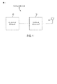
[0027]ワイヤレスデバイス100は、ベースバンドプロセッサ102と、ワイヤレストランシーバ104と、アンテナ106とを含む。ワイヤレストランシーバ104は、送信機能と受信機能の両方をサポートするために1つまたは複数のLO信号を生成するために、本開示全体にわたって提示される位相ロックループの様々な態様を採用し得る。ワイヤレストランシーバ104は、アンテナ106を通したワイヤレスチャネルを介した送信のために、1つまたは複数のキャリア信号を、ベースバンドプロセッサ102によって生成されたデータで変調することによって、送信機能を実行する。ワイヤレストランシーバ104は、ベースバンドプロセッサ102によるさらなる処理のためにデータを復元するために、アンテナ106を通してワイヤレスチャネルから受信された1つまたは複数のキャリア信号を復調することによって、受信機能を実行する。ベースバンドプロセッサ102は、ワイヤレスチャネルへの物理および電気的インターフェースに従ってデータを送信および受信するための物理レイヤ、ワイヤレスチャネルへのアクセスを管理するためのデータリンクレイヤ、ソース・宛先間データ転送を管理するためのネットワークレイヤ、エンドユーザ間のデータの透過的な転送を管理するためのトランスポートレイヤ、ならびにワイヤレスチャネルを通してネットワークへの接続を確立またはサポートするために必要なまたは望ましい任意の他のレイヤを例として含む、ワイヤレス通信をサポートするために必要とされる基本プロトコルスタックを与える。
[0027] The wireless device 100 includes a
[0028]図2は、ワイヤレストランシーバの例示的な実施形態のブロック図である。ワイヤレストランシーバ104は、双方向通信をサポートする送信機200と受信機250とを含む。送信機200および/または受信機250は、スーパーヘテロダイン・アーキテクチャまたは直接変換アーキテクチャを用いて実装され得る。スーパーヘテロダイン・アーキテクチャでは、信号が、複数の段においてRFとベースバンドとの間で、(たとえば、受信機について、1つの段においてRFから中間周波数(IF)に、次いで別の段においてIFからベースバンドに)周波数変換される。ゼロIFアーキテクチャとも呼ばれる直接変換アーキテクチャでは、信号が、1つの段においてRFとベースバンドとの間で周波数変換される。スーパーヘテロダイン・アーキテクチャおよび直接変換アーキテクチャは、異なる回路ブロックを使用し、および/または異なる要件を有し得る。図2に示されている例示的な実施形態では、送信機200および受信機250は直接変換アーキテクチャを用いて実装される。
[0028] FIG. 2 is a block diagram of an exemplary embodiment of a wireless transceiver. The
[0029]送信経路では、ベースバンドプロセッサ104(図1参照)は、デジタル・アナログ変換器(DAC)202にデータを与える。DAC202は、デジタル入力信号をアナログ出力信号に変換する。アナログ出力信号は、DAC202による前のデジタル・アナログ変換によって生じたイメージを除去するためにアナログ出力信号をフィルタ処理する、フィルタ204に与えられる。増幅器206が、増幅されたベースバンド信号を与えるために、フィルタ204からの信号を増幅するために使用される。ミキサ208が、増幅されたベースバンド信号とTX局部発振器210からのLO信号とを受信する。ミキサ208は、アップコンバートされた信号を与えるために、増幅されたベースバンド信号をLO信号と混合する。フィルタ212が、周波数混合(frequency mixing)によって生じたイメージを除去するために、アップコンバートされた信号をフィルタ処理するために使用される。電力増幅器(PA)214が、所望の出力電力レベルにおける出力RF信号を取得するために、フィルタ212からの信号を増幅するために使用される。出力RF信号は、ワイヤレスチャネルを介した送信のために、デュプレクサ260を通してアンテナ106にルーティングされる。
[0029] In the transmit path, baseband processor 104 (see FIG. 1) provides data to digital-to-analog converter (DAC) 202. The
[0030]受信経路では、アンテナ106は、リモートデバイスによって送信された信号を受信し得る。受信RF信号は、デュプレクサ260を通して受信機250にルーティングされ得る。受信機250内で、受信RF信号は、入力RF信号を取得するために、低雑音増幅器(LNA)252によって増幅され、フィルタ254によってフィルタ処理される。ミキサ256が、入力RF信号と、RX局部発振器258からのLO信号とを受信する。ミキサ256は、ダウンコンバートされた信号を与えるために、入力RF信号をLO信号と混合する。ダウンコンバートされた信号は、増幅されたダウンコンバートされた信号を取得するために、増幅器260によって増幅される。フィルタ262が、周波数混合によって生じたイメージを除去するために、増幅されたダウンコンバートされた信号をフィルタ処理するために使用される。フィルタ262からの信号は、アナログ・デジタル変換器(ADC)264に与えられる。ADC264は、その信号をデジタル出力信号に変換する。デジタル出力信号は、ベースバンドプロセッサ104(図1参照)に与えられ得る。
[0030] In the receive path,
[0031]送信機200および受信機250における信号の調整は、増幅器、フィルタ、ミキサなどの1つまたは複数の段によって実行され得る。これらの回路は、図2に示されている構成とは異なってアレンジされ(arranged)得る。さらに、図2に示されていない他の回路も送信機200および受信機250において信号を調整するために使用され得る。たとえば、インピーダンス整合回路が、PA216の出力において、LNA252の入力において、アンテナ106とデュプレクサ260との間などに配置され得る。
[0031] Conditioning of the signals at
[0032]送信機および受信機機能をサポートするために、局部発振器の様々な実施形態が使用され得る。例示的な一実施形態では、局部発振器は、混合のために送信機および/または受信機にLO信号を与えるVCOを用いて実装され得る。VCOは、フィードバックループ中の同調共振器(tuned resonator)を有する正のフィードバック増幅器である。発振は共振周波数(resonant frequency)において生じ、共振周波数は位相ロックループによって同調させられ得る。位相ロックループは、VCO出力の位相を基準信号の位相と比較し、位相を整列された状態に保つようにVCOの共振器を同調させる、位相検出器を用いて実装され得る。 [0032] Various embodiments of the local oscillator may be used to support transmitter and receiver functions. In an exemplary embodiment, the local oscillator may be implemented with a VCO that provides a LO signal to the transmitter and / or receiver for mixing. The VCO is a positive feedback amplifier with a tuned resonator in the feedback loop. Oscillation occurs at a resonant frequency, which can be tuned by a phase locked loop. The phase locked loop may be implemented with a phase detector that compares the phase of the VCO output with the phase of the reference signal and tunes the resonator of the VCO to keep the phase aligned.
[0033]図3は、局部発振器のための位相ロックループの例示的な実施形態を示す機能ブロック図である。この実施形態では、局部発振器は、位相ロックループ300を用いて実装される。位相ロックループ300は、位相検出器302と、電荷ポンプ304と、ループフィルタ306と、VCO308と、周波数分割器312およびシグマデルタ変調器314を有するフラクショナルN周波数分割器(fractional-N frequency divider)310とを含む。位相検出器302は、2つの入力信号間の位相差を検出するための手段を与える。位相検出器302は、基準信号とフラクショナルN周波数分割器310からのフィードバック信号との間の位相誤差を検出するために使用される。位相検出器302は、位相誤差に基づいてアップ信号とダウン信号とを生成する。アップ信号およびダウン信号は、電荷ポンプ304を駆動するために使用される。電荷ポンプ304は、ループフィルタ306に電流源を与えるための手段を与える。電荷ポンプ304は、検出された位相誤差に比例する電荷をループフィルタ306に注入する。ループフィルタ306は、VCO308を同調させるための制御電圧を生成するための手段を与える。ループフィルタ306は、VCO308に入力される制御電圧を生成するために、電荷ポンプ304からの出力を積分する(integrate)。VCO308は、同調可能周波数を有する発振信号を生成するための手段を与える。VCO308は、それの周波数が、ループフィルタ306によって生成された制御電圧に比例する発振信号を生成する。フラクショナルN周波数分割器310は、発振信号の周波数をフラクショナルに分割する(fractionally dividing)ことによって、フィードバック信号を生成するための手段を与える。フラクショナルN周波数分割器310は、位相検出器へのフィードバック信号入力を生成するために、VCO出力の周波数を整数Nで分割する周波数分割器312を含む。フラクショナルN周波数分割器310はまた、NからN+1の間の非整数である平均分割器を実現するために、ロック状態中に(during the locked state)Nの値を動的に切り替えるデルタシグマ変調器314を含む。
[0033] FIG. 3 is a functional block diagram illustrating an exemplary embodiment of a phase locked loop for a local oscillator. In this embodiment, the local oscillator is implemented using the phase locked loop 300. The phase locked loop 300 includes a
[0034]図4Aは、電荷ポンプおよびループフィルタのための追加の概略図詳細をもつ、局部発振器のための位相ロックループの例示的な実施形態を示す機能ブロック図である。上記で説明したように、位相検出器302は、基準信号をフラクショナルN周波数分割器310からのフィードバック信号と比較し、2つの信号間の位相差に基づいて電荷ポンプ304をアクティブにする。位相検出器302は、位相検出モードおよび位相ロック状態において動作する。このために、位相検出器は、位相/周波数検出器(PFD:phase/frequency detector)と呼ばれることがある。本開示では、「位相検出器」という用語は、2つの入力信号の位相および/または周波数における差を検出することが可能な構成要素を含むように広く解釈されるものとする。
[0034] FIG. 4A is a functional block diagram illustrating an exemplary embodiment of a phase-locked loop for a local oscillator with additional schematic details for the charge pump and loop filter. As explained above, the
[0035]位相検出器302は、位相検出器302によって測定された位相誤差に基づいて、アップ信号およびダウン信号のデューティサイクルが変化させられる、位相検出モードにおいて動作する。その結果、電荷ポンプ304は、2つの信号間の位相差に比例する、時間の一部分の間のみアクティブにされる。ループフィルタ306は、位相差が0に達するまで、VCO出力信号の周波数を調整するフィルタ処理された制御電圧を生成する電荷を蓄積する。これが生じると、位相検出器302は位相ロック状態に入る。この状態では、アップ信号のデューティサイクルとダウン信号のデューティサイクルとは実質的に等しく、したがって、正味電荷(net charge)はループフィルタ306に注入されない。VCO308への制御電圧入力は一定のままであり、それは、VCO出力信号が一定の周波数のままであることを保証する。
[0035] The
[0036]ループフィルタ306は、アクティブまたはパッシブであり得る。パッシブループフィルタ306の例示的な実施形態が、図4に示されている。この実施形態では、ループフィルタ306は、電荷ポンプ304出力と負電源電圧VSS(たとえば、接地)との間に直列に接続された抵抗R408とキャパシタC410とを備える、1次ループフィルタ(first order loop filter)を備える。ループフィルタの代替実施形態も採用され得る。たとえば、ループフィルタ306は、抵抗R408およびキャパシタC410に並列に接続された余分の極キャパシタ(extra pole capacitor)409を含み得る。
[0036] The
[0037]電荷ポンプ304は、いくつかの方法でも実装され得る。例示的な一実施形態では、電荷ポンプ304は、充電電流(a charge current)をループフィルタ306にソースする(sourcing)ための手段を与える第1のスイッチ404と、放電電流(discharge current)をループフィルタ306からシンクする(sinking)ための手段を与える第2のスイッチ406とを用いて実装される。第1のスイッチ404は、PMOSトランジスタであり得、第2のスイッチ406は、NMOSトランジスタ406であり得る。PMOSトランジスタは、電流源405を介して正電源電圧VDDに接続される。NMOSトランジスタは、図4Aに示されているような電流源407を介して、負電源電圧VSSに接続される。電流源405および407は、電荷ポンプ304に定電流源を与える。位相検出器302からのアップ信号は、インバータ402を通してPMOSトランジスタ404を制御し、位相検出器302からのダウン信号は、NMOSトランジスタを制御する。アップ信号が位相検出器302によって高論理レベル状態に駆動されるとき、ループフィルタ306中のキャパシタC410はPMOSトランジスタ404を通して充電される。ダウン信号が位相検出器202によって高論理レベル状態に駆動されるとき、ループフィルタ306中のキャパシタC410はNMOSトランジスタ406を通して放電される。余分の極キャパシタ409は、ループフィルタ306をさらに調整するために、抵抗R408およびキャパシタC410と並列に追加される。
[0037] The
[0038]図4Bは、電荷ポンプ中の漏れ電流源を追加した、図4Aの局部発振器のための位相ロックループの例示的な実施形態を示す機能ブロック図である。漏れ電流源は、ループフィルタ306に漏れ電流を与えるための手段を与える。この実施形態では、フラクショナルN位相ロックループ(fractional-N phase locked loop)における電荷ポンプ302の非線形性により場合によっては生じるであろう近傍オフセット周波数(close-in offset frequencies)におけるデルタシグマ変調器の雑音重畳(noise folding)を回避するために、漏れ電流源410が使用される。漏れ電流源412は、適切なバイアシング(appropriate biasing)をもつ1つまたは複数のトランジスタを用いて、または他の好適な手段によって実装され得る。漏れ電流源410は、ロック状態にある位相検出器302に入力される基準信号とフィードバック信号との間の一定の平均位相差を生じさせる。その結果、漏れ電流がどのように実装されるかに応じて、アップ信号またはダウン信号のうちの一方が他方よりも高いデューティサイクルを常に有する。いくつかの実施形態では、より広いパルスが位相差に等しい幅を維持する間、より狭いパルスが連続的「低」論理状態に駆動され得る。この手法では、電荷ポンプ302において電流源のスイッチングがなく、それにより、雑音を減少させる。
[0038] FIG. 4B is a functional block diagram illustrating an exemplary embodiment of a phase-locked loop for the local oscillator of FIG. 4A with the addition of a leakage current source in the charge pump. The leakage current source provides a means for providing leakage current to
[0039]図5は、位相ロックループのための位相検出器の例示的な実施形態を示す機能ブロック図である。この実施形態では、位相検出器302は、2つの段、すなわち第1の段502と第2の段504とを含む。第1の段502は、基準信号とフィードバック信号との間の位相差に基づいて、アップ信号とダウン信号とを生成する。第2の段504は、アップ信号またはダウン信号のどの信号がより低いデューティサイクルを有するかに応じて、アップ信号またはダウン信号のいずれかを低論理状態(low logic state)に駆動する。
[0039] FIG. 5 is a functional block diagram illustrating an exemplary embodiment of a phase detector for a phase locked loop. In this embodiment, the
[0040]第1の段502は、第1のフリップフロップ506と、第2のフリップフロップ508と、リセットゲート510と、遅延511とを含む。この実施形態では、フリップフロップ506とフリップフロップ508の両方がDフリップフロップであり、リセットゲート510がANDゲートであるが、代替実施形態では、他のフリップフロップ、ゲート、および/または構成要素が使用、追加、および/または省略され得る。フリップフロップ506とフリップフロップ508の両方への入力は、VDD(すなわち、高論理状態(high logic state))にプルアップされる。第1のフリップフロップ506をクロック制御する(clock)ために基準信号が使用され、第2のフリップフロップ508をクロック制御するためにフィードバックが使用される。その結果、基準信号が高論理状態に遷移するとき、第1のフリップフロップ506の出力Q1が高論理状態に駆動され、フィードバック信号が高論理状態に遷移するとともに、第2のフリップフロップ508の出力Q2が高論理状態に駆動される。リセットゲート510は、フリップフロップ506および508からの2つの出力のための「AND」機能を与えるために使用される。フリップフロップ506からの出力とフリップフロップ508からの出力の両方が、適切な遅延の後に高論理状態に入ると、フリップフロップ506とフリップフロップ508の両方をリセットするために、リセットゲート510からの出力が使用される。
[0040] The
[0041]第2の段504は、第1のゲート512と、第2のゲート514と、第1のインバータ516と、第2のインバータ518とを備える、ゲーティング回路(gating circuit)を含む。第1のゲート512は、アップ信号を生成するために使用され、第2のゲート514は、ダウン信号を生成するために使用される。一実施形態では、ゲート512とゲート514の両方がANDゲートであるが、代替実施形態では異なって実装され得る。たとえば、各ゲートは、代替的に、他の好適な手段によって、またはインバータによって続かれるNANDゲートとして実装され得る。各ゲート512および514は、第2の入力が高論理状態にあるとき、第1の入力における信号を出力にパスするように機能する。したがって、各ゲート512および514への第2の入力は、イネーブル信号と見なされ得る。すなわち、イネーブル信号が高論理状態にあるとき、各ゲート512および514は第1の入力における信号を出力にパスする。イネーブル信号が低論理状態にあるとき、出力は第1の入力の状態にかかわらず低く強制される(forced low)。第1のインバータ516および第2のインバータ518は、イネーブル信号を生成するために使用される。詳細には、第1のインバータ516は、第1のゲート512へのイネーブル信号を生成するために使用され、第2のインバータ518は、第2のゲート514へのイネーブル信号を生成するために使用される。説明する実施形態では、第1のゲート512のためのイネーブル信号は、第2のフリップフロップ508の反転出力(inverted output)Q2であり、第2のゲート514のためのイネーブル信号は、第1のフリップフロップ506の反転出力Q1である。
[0041] The second stage 504 includes a gating circuit that includes a
[0042]動作中、第2のフリップフロップ508からの出力Q2が低論理状態にあるとき、第1のフリップフロップ506からの出力Q1がアップ信号として第1のゲート512を通してパスされる。第2のフリップフロップ508からの出力Q2が高論理状態にあるとき、第1のゲート512から出力されたアップ信号が低論理状態に強制される。同様に、第1のフリップフロップ506からの出力Q1が低論理状態にあるとき、第2のフリップフロップ508からの出力Q2がダウン信号として第2のゲート514を通してパスされる。第1のフリップフロップ506からの出力Q1が高論理状態にあるとき、第2のゲート514から出力されたダウン信号が低論理状態に強制される。
[0042] In operation, when the output Q2 from the second flip-
[0043]図6Aおよび図6Bは、図5の位相ロックループの例示的な実施形態の動作を示すタイミング図である。図6Aに、基準信号が周波数分割器からのフィードバック信号に先行するときの、位相検出器のタイミングを示す。図6Bに、基準信号がフィードバック信号に後続するときの、位相検出器のタイミングを示す。 [0043] FIGS. 6A and 6B are timing diagrams illustrating operation of an exemplary embodiment of the phase locked loop of FIG. FIG. 6A shows the timing of the phase detector when the reference signal precedes the feedback signal from the frequency divider. FIG. 6B shows the timing of the phase detector when the reference signal follows the feedback signal.
[0044]図5および図6Aを参照すると、第1のフリップフロップ506からの出力Q1と第2のフリップフロップ508からの出力Q2の両方が、t0において低論理状態にある。その結果、第1のゲート512と第2のゲート514の両方は、それぞれ、インバータ516および518からの反転されたフリップフロップ出力Q1およびQ2によって有効にされる。第1のゲート512が有効にされると、低論理状態におけるアップ信号を生成するために、第1のフリップフロップ506からの低論理状態出力Q1が第1のゲート512を通して出力にパスされる。第2のゲート514が有効にされると、低論理状態におけるダウン信号を生成するために、第2のフリップフロップ506からの低論理状態出力Q2が第2のゲート514を通して出力にパスされる。
[0044] Referring to FIGS. 5 and 6A, both the output Q1 from the first flip-
[0045]t1において、基準信号が低論理状態から高論理状態に遷移し、それにより、第1のフリップフロップ506の出力Q1を高論理状態に設定する。アップ信号を高論理状態に駆動するために、高論理状態が第1のゲート512を通して出力にパスされる。同時に、第2のインバータ518からの反転されたフリップフロップ出力Q1が低論理状態に遷移し、それにより、第2のゲート514を無効にする。
In [0045] t 1, the reference signal transitions from a low logic state to a high logic state, thereby setting the output Q1 of the first flip-
[0046]t2において、フィードバック信号が低論理状態から高論理状態に遷移し、それにより、第2のフリップフロップ508の出力Q2を高論理状態に設定する。第2のゲート514が無効にされるので、第2のフリップフロップ508からの出力Q2の高論理状態は第2のゲート514を通してパスされない。その結果、ダウン信号は、低論理状態にあるままである。第1のインバータ516からの反転されたフリップフロップ出力Q2が低論理状態に遷移し、それにより、第1のゲート512を無効にし、アップ信号を低論理状態に強制する。出力Q1と出力Q2の両方が高論理状態にあると、リセットゲート510からの出力は、高論理状態に遷移し、t3において適切な遅延の後にフリップフロップ506とフリップフロップ508の両方をリセットする。フリップフロップ506とフリップフロップ508の両方がリセットされると、インバータ516および518からの反転されたフリップフロップ出力Q1およびQ2が高論理状態に駆動され、それにより、次のサイクルの間、第1のゲート512と第2のゲート514の両方を有効にする。このプロセスは、フィードバック信号を基準信号に整列させることによって位相ロックループがロックを達成するまで続く。
In [0046] t 2, the feedback signal transitions from a low logic state to a high logic state, thereby setting the output Q2 of the second flip-
[0047]図5および図6Bを参照すると、第1のフリップフロップ506からの出力Q1と第2のフリップフロップ508からの出力Q2の両方は、t0において低論理状態にある。その結果、第1のゲート512と第2のゲート514の両方は、それぞれ、インバータ516および518からの反転されたラッチ出力(inverted latch outputs)Q1およびQ2によって有効にされる。第1のゲート512が有効にされると、低論理状態におけるアップ信号を生成するために、第1のフリップフロップ506からの低論理状態出力Q1が第1のゲート512を通して出力にパスされる。第2のゲート514が有効にされると、低論理状態におけるダウン信号を生成するために、第2のフリップフロップ506からの低論理状態出力Q2が第2のゲート514を通して出力にパスされる。
[0047] Referring to FIGS. 5 and 6B, both the output Q1 from the first flip-
[0048]t1において、フィードバック信号が低論理状態から高論理状態に遷移し、それにより、第2のフリップフロップ508の出力Q2を高論理状態に設定する。ダウン信号を高論理状態に駆動するために、高論理状態が第2のゲート514を通して出力にパスされる。同時に、第1のインバータ516からの反転されたフリップフロップ出力Q2が低論理状態に遷移し、それにより、第1のゲート512を無効にする。
In [0048] t 1, the feedback signal transitions from a low logic state to a high logic state, thereby setting the output Q2 of the second flip-
[0049]t2において、基準信号が低論理状態から高論理状態に遷移し、それにより、第1のフリップフロップ506の出力Q1を高論理状態に設定する。第1のゲート512が無効にされるので、第1のフリップフロップ506からの出力Q1の高論理状態は第1のゲート512を通してパスされない。その結果、アップ信号は、低論理状態にあるままである。第2のインバータ518からの反転されたフリップフロップ出力Q1が低論理状態に遷移し、それにより、第2のゲート514を無効にし、ダウン信号を低論理状態に強制する。出力Q1と出力Q2の両方が高論理状態にあると、リセットゲート510からの出力は、高論理状態に遷移し、t3において適切な遅延の後にフリップフロップ506とフリップフロップ508の両方をリセットする。フリップフロップ506とフリップフロップ508の両方がリセットされると、インバータ516および518からの反転されたフリップフロップ出力Q1およびQ2が高論理状態に駆動され、それにより、次のサイクルの間、第1のゲート512と第2のゲート514の両方を有効にする。このプロセスは、フィードバック信号を基準信号に整列させることによって位相ロックループがロックを達成するまで続く。
In [0049] t 2, the reference signal transitions from a low logic state to a high logic state, thereby setting the output Q1 of the first flip-
[0050]図7は、位相ロックループのための位相検出器の代替の例示的な実施形態を示す機能ブロック図である。この実施形態では、第2の段におけるインバータは、NANDゲートと交換される。詳細には、第1のインバータ516(図5参照)が第1のNANDゲート716と交換され、第2のインバータ518(図5参照)が第2のNANDゲート718と交換される。NANDゲート716および718は、モードビットが2つの異なる動作モード間で位相検出器302を切り替えることを可能にする。モードビットが高論理状態に設定されると、NANDゲート716および718はインバータとして機能し、位相検出器の動作が、図5、図6Aおよび図6Bに関して上記で説明したのと同じである。モードビットが低論理状態に駆動されると、NANDゲート716とNANDゲート718の両方からの出力は、それぞれ、第1のフリップフロップ506の出力Q1および第2のフリップフロップ508の出力Q2の状態にかかわらず、常に高論理状態にある。その結果、第1のゲート512および第2のゲート514が常に有効にされる。ゲート512とゲート514の両方が有効にすると、アップ信号が第1のフリップフロップ506からの出力Q1に後続し(follow)、ダウン信号が第2のフリップフロップ508からの出力Q2に後続する。このモードでは、アップ信号とダウン信号の両方が、各サイクル、パルス化される(pulsed each cycle)ことになる。
[0050] FIG. 7 is a functional block diagram illustrating an alternative exemplary embodiment of a phase detector for a phase locked loop. In this embodiment, the inverter in the second stage is replaced with a NAND gate. Specifically, the first inverter 516 (see FIG. 5) is replaced with the
[0051]ここまで説明した位相検出器の例示的な実施形態では、より低いデューティサイクルをもつアップ信号またはダウン信号は、ゲートオフされる(gated off)(すなわち、低論理状態に強制される)。しかしながら、より低いデューティサイクルをもつ信号は、ゲーティング以外の手段によって低論理状態に強制され得る。たとえば、ダウン信号に対するアップ信号のデューティサイクルに応じてアップ信号と低論理状態との間で切り替えるために、マルチプレクサが使用され得る。同様に、アップ信号に対してダウン信号のデューティサイクルに応じてダウン信号と低論理状態との間で切り替えるために、マルチプレクサが使用され得る。代替的に、いくつかの例示的な実施形態では、より低いデューティサイクルをもつアップ信号またはダウン信号は、信号を高論理状態に駆動することによってオフにされ(turned off)得る。当業者は、特定の適用例とシステムに課される全体的な設計制約とに応じて、最も低いデューティサイクルをもつアップ信号またはダウン信号のターンオフ(turn off)を強制するように、様々な回路構成を容易に設計することができよう。 [0051] In the exemplary embodiment of the phase detector described thus far, an up or down signal with a lower duty cycle is gated off (ie, forced to a low logic state). However, signals with lower duty cycles may be forced to a low logic state by means other than gating. For example, a multiplexer may be used to switch between the up signal and a low logic state depending on the duty cycle of the up signal relative to the down signal. Similarly, a multiplexer can be used to switch between the down signal and a low logic state for the up signal depending on the duty cycle of the down signal. Alternatively, in some exemplary embodiments, an up or down signal with a lower duty cycle may be turned off by driving the signal to a high logic state. Those of ordinary skill in the art will appreciate that various circuits may be forced to force the turn off of the up or down signal with the lowest duty cycle, depending on the particular application and the overall design constraints imposed on the system. The configuration could easily be designed.
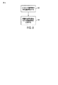
[0052]図8は、発振信号を生成する例示的な方法を示すフローチャートである。 [0052] FIG. 8 is a flow chart illustrating an exemplary method of generating an oscillating signal.
[0053]方法は、ブロック802において、2つの入力信号間の位相差を検出することを含む。位相差は、位相差に応答して第1および第2の信号を出力することによって検出され得、ここで、第2の信号を出力するときに第1の信号が無効にされ、第1の信号を出力するときに第2の信号が無効にされる。例示的な一実施形態では、第2の信号を出力するときに第1の信号を無効にすることと、第1の信号を出力するときに第2の信号を無効にすることとを行うために、ゲーティング回路が使用され得る。2つの入力信号は、基準信号とフィードバック信号とを備え得る。フィードバック信号は、発振信号の関数である。例示的な一実施形態では、フィードバック信号は、発振信号の周波数をフラクショナルに分割することによって生成され得る。 [0053] The method includes, at block 802, detecting a phase difference between the two input signals. The phase difference may be detected by outputting the first and second signals in response to the phase difference, wherein the first signal is nullified when outputting the second signal and the first signal is output. The second signal is disabled when outputting the signal. In one exemplary embodiment, for disabling the first signal when outputting the second signal and disabling the second signal when outputting the first signal. For that, a gating circuit can be used. The two input signals may comprise a reference signal and a feedback signal. The feedback signal is a function of the oscillating signal. In one exemplary embodiment, the feedback signal may be generated by fractionally dividing the frequency of the oscillator signal.
[0054]方法は、ブロック804において、第1の信号および第2の信号に応答して、同調可能周波数を有する発振信号を生成することをさらに含む。発振信号の周波数を同調させるために、制御電圧が使用され得る。制御電圧を生成するために、電流源が使用され得る。電流源は、第1の信号に応答して充電電流をソースし、第2の信号に応答して放電電流をシンクし得る。制御電圧は、充電電流および放電電流を積分することによって生成され得る。制御電圧の生成において漏れ電流源も使用され得る。 [0054] The method further includes, at block 804, generating an oscillating signal having a tunable frequency in response to the first signal and the second signal. A control voltage may be used to tune the frequency of the oscillating signal. A current source can be used to generate the control voltage. The current source may source the charging current in response to the first signal and sink the discharging current in response to the second signal. The control voltage can be generated by integrating the charge current and the discharge current. Leakage current sources may also be used in the generation of the control voltage.
[0055]上記で説明した動作方法におけるブロックの特定の順序または階層は、一例として与えられたにすぎない。設計選好に基づいて、動作方法におけるブロックの特定の順序または階層は、並べ替えられ、修正され、および/または変更され得る。添付の方法クレームは、動作方法に関係する様々な限定を含むが、具陳された限定は、特許請求の範囲において明記されていない限り、特定の順序または階層によっていかなる形でも限定されるものではない。 [0055] The particular order or hierarchy of blocks in the methods of operation described above is provided as an example only. Based on design preferences, the particular order or hierarchy of blocks in a method of operation may be rearranged, modified, and / or changed. The accompanying method claims include various limitations relating to the manner of operation, but the stated limitations are not to be limited in any way by any particular order or hierarchy, unless explicitly stated in the claims. Absent.
[0056]以上の説明は、いかなる当業者も本開示の全範囲を完全に理解することができるように与えたものである。本明細書で開示する様々な例示的な実施形態への変更は当業者には容易に明らかであろう。したがって、特許請求の範囲は、本明細書で説明した本開示の様々な態様に限定されるべきではなく、特許請求の範囲の言い回しに矛盾しない全範囲を与えられるものとする。当業者に知られている、または後に知られることになる、本開示全体にわたって説明した様々な態様の要素のすべての構造的および機能的均等物は、参照により本明細書に明確に組み込まれ、特許請求の範囲に包含されるものである。さらに、本明細書で開示するいかなることも、そのような開示が特許請求の範囲に明示的に具陳されているかどうかにかかわらず、公に供するものではない。いかなるクレーム要素も、その要素が「ための手段」という句を使用して明確に具陳されていない限り、または方法クレームの場合には、その要素が「ためのステップ」という句を使用して具陳されていない限り、米国特許法第112条(f)の規定の下で解釈されるべきではない。
以下に、本願の出願当初の特許請求の範囲に記載された発明を付記する。
[C1]
発振信号を生成するための回路であって、
2つの入力信号間の位相差に応答して第1の信号および第2の信号を出力するように構成された位相検出器と、前記位相検出器が、前記第2の信号を出力するときに前記第1の信号を無効にすることと、前記第1の信号を出力するときに前記第2の信号を無効にすることとを行うようにさらに構成された、
前記第1の信号および前記第2の信号に応答して、同調可能周波数を有する発振信号を生成するように構成された電圧制御発振器(VCO)と
を備える、回路。
[C2]
電荷ポンプとループフィルタとをさらに備え、ここにおいて、前記電荷ポンプが、前記第1の信号に応答して充電電流をソースすることと、前記第2の信号に応答して放電電流をシンクすることとによって前記ループフィルタに電流源を与えるように構成された、C1に記載の回路。
[C3]
前記ループフィルタが、前記VCOの前記周波数を同調させるための制御電圧を生成するために、前記充電電流および前記放電電流を積分するように構成された、C2に記載の回路。
[C4]
前記電荷ポンプが、前記ループフィルタに結合された漏れ電流源をさらに備える、C2に記載の回路。
[C5]
前記位相検出器が、前記第2の信号を出力するときに前記第1の信号を無効にすることと、第1の信号を出力するときに前記第2の信号を無効にすることとを行うように構成されたゲーティング回路を備える、C1に記載の回路。
[C6]
前記2つの入力信号が、基準信号とフィードバック信号とを備え、前記フィードバック信号が、前記発振信号から導出される、C1に記載の回路。
[C7]
前記発振信号から前記フィードバック信号を生成するように構成されたフラクショナルN分割器をさらに備える、C6に記載の回路。
[C8]
発振信号を生成するための回路であって、
2つの入力信号間の位相差を検出するための手段と、ここにおいて、位相差を検出するための前記手段が、2つの入力信号間の前記位相差に応答して第1の信号および第2の信号を出力するように構成され、ここにおいて、位相差を検出するための前記手段が、前記第2の信号を出力するときに前記第1の信号を無効にすることと、前記第1の信号を出力するときに前記第2の信号を無効にすることとを行うようにさらに構成された、
前記第1の信号および前記第2の信号に応答して、同調可能周波数を有する発振信号を生成するための手段と
を備える、回路。
[C9]
前記発振信号の前記周波数を同調させるための制御電圧を生成するための手段、前記第1の信号に応答して充電電流をソースするための手段および前記第2の信号に応答して放電電流をシンクするための手段を備える制御電圧を生成するための前記手段に電流源を与えるための手段、をさらに備える、C8に記載の回路。
[C10]
制御電圧を生成するための前記手段が、前記発振信号の前記周波数を同調させるための前記制御電圧を生成するために、前記充電電流および前記放電電流を積分するように構成された、C9に記載の回路。
[C11]
電流源を与えるための前記手段が、制御電圧を生成するための前記手段に漏れ電流を与えるための手段をさらに備える、C9に記載の回路。
[C12]
位相差を検出するための前記手段が、前記第2の信号を出力するときに前記第1の信号を無効にすることと、第1の信号を出力するときに前記第2の信号を無効にすることとを行うように構成されたゲーティング回路を備える、C8に記載の回路。
[C13]
前記2つの入力信号が、基準信号とフィードバック信号とを備え、前記フィードバック信号が、前記発振信号の関数である、C8に記載の回路。
[C14]
前記発振信号の前記周波数をフラクショナルに分割することによって、前記フィードバック信号を生成するための手段をさらに備える、C13に記載の回路。
[C15]
発振信号を生成する方法であって、
2つの入力信号間の位相差を検出することと、前記検出することが、第2の信号を出力するときに第1の信号を無効にすることと、前記第1の信号を出力するときに前記第2の信号を無効にすることとによって、2つの入力信号間の前記位相差に応答して前記第1の信号および前記第2の信号を出力することを備える、
前記第1の信号および前記第2の信号に応答して、同調可能周波数を有する発振信号を生成することと
を備える、方法。
[C16]
前記発振信号の前記周波数を同調させるための制御電圧を生成することと、前記第1の信号に応答して充電電流をソースすることと、前記第2の信号に応答して放電電流をシンクすることとによって、前記制御電圧を生成するための電流源を与えることとをさらに備える、C15に記載の方法。
[C17]
制御電圧を前記生成することが、前記充電電流および前記放電電流を積分することを備える、C16に記載の方法。
[C18]
制御電圧を前記生成することに漏れ電流を与えることをさらに備える、C16に記載の方法。
[C19]
位相差を前記検出することが、前記第2の信号を出力するときに前記第1の信号を無効にすることと、第1の信号を出力するときに前記第2の信号を無効にすることとを行うためにゲーティング回路を使用することを備える、C15に記載の方法。
[C20]
前記2つの入力信号が、基準信号とフィードバック信号とを備え、前記フィードバック信号が、前記発振信号の関数である、C15に記載の方法。
[C21]
前記発振信号の前記周波数をフラクショナルに分割することによって、前記フィードバック信号を生成することをさらに備える、C20に記載の方法。
[0056] The above description is provided to enable any person skilled in the art to fully understand the full scope of the disclosure. Modifications to the various exemplary embodiments disclosed herein will be readily apparent to those skilled in the art. Therefore, the scope of the claims should not be limited to the various aspects of the present disclosure described herein, but rather should be given the full scope consistent with the wording of the claims. All structural and functional equivalents of elements of the various aspects described throughout this disclosure that are known to, or will be known to, those of skill in the art are expressly incorporated herein by reference, It is intended to fall within the scope of the claims. Furthermore, nothing disclosed herein is made publicly available, regardless of whether such disclosure is expressly set forth in the claims. Any claim element is not explicitly stated using the phrase "means for", or in the case of a method claim, the element uses the phrase "step for" Unless otherwise stated, it should not be construed under the provisions of 35 USC 112 (f).
The inventions described in the claims at the initial application of the present application will be additionally described below.
[C1]
A circuit for generating an oscillating signal,
A phase detector configured to output a first signal and a second signal in response to a phase difference between two input signals; and when the phase detector outputs the second signal. Further configured to disable the first signal and disable the second signal when outputting the first signal,
A voltage controlled oscillator (VCO) configured to generate an oscillating signal having a tunable frequency in response to the first signal and the second signal.
A circuit.
[C2]
Further comprising a charge pump and a loop filter, wherein the charge pump sources a charging current in response to the first signal and sinks a discharging current in response to the second signal. The circuit according to C1, configured to provide a current source to the loop filter by.
[C3]
The circuit of C2, wherein the loop filter is configured to integrate the charging current and the discharging current to generate a control voltage for tuning the frequency of the VCO.
[C4]
The circuit of C2, wherein the charge pump further comprises a leakage current source coupled to the loop filter.
[C5]
The phase detector invalidates the first signal when outputting the second signal and invalidates the second signal when outputting the first signal. The circuit according to C1, comprising a gating circuit configured to:
[C6]
The circuit of C1, wherein the two input signals comprise a reference signal and a feedback signal, the feedback signal being derived from the oscillating signal.
[C7]
The circuit of C6, further comprising a fractional N divider configured to generate the feedback signal from the oscillator signal.
[C8]
A circuit for generating an oscillating signal,
Means for detecting a phase difference between two input signals, wherein said means for detecting a phase difference are responsive to said phase difference between two input signals for a first signal and a second signal. Wherein the means for detecting a phase difference invalidates the first signal when outputting the second signal; and And further disabling the second signal when outputting a signal,
Means for generating an oscillating signal having a tunable frequency in response to the first signal and the second signal;
A circuit.
[C9]
Means for generating a control voltage for tuning the frequency of the oscillating signal, means for sourcing a charging current in response to the first signal and a discharging current in response to the second signal. The circuit of C8, further comprising: means for providing a current source to said means for generating a control voltage, comprising means for sinking.
[C10]
C9, wherein the means for generating a control voltage is configured to integrate the charging current and the discharging current to generate the control voltage for tuning the frequency of the oscillating signal. Circuit.
[C11]
The circuit of C9, wherein the means for providing a current source further comprises means for providing leakage current to the means for generating a control voltage.
[C12]
The means for detecting a phase difference invalidates the first signal when outputting the second signal, and invalidates the second signal when outputting the first signal The circuit of C8, comprising a gating circuit configured to:
[C13]
The circuit of C8, wherein the two input signals comprise a reference signal and a feedback signal, the feedback signal being a function of the oscillating signal.
[C14]
The circuit of C13, further comprising means for generating the feedback signal by fractionally dividing the frequency of the oscillating signal.
[C15]
A method of generating an oscillating signal,
Detecting a phase difference between two input signals, said detecting invalidating a first signal when outputting a second signal, and outputting the first signal Disabling the second signal to output the first signal and the second signal in response to the phase difference between two input signals.
Generating an oscillating signal having a tunable frequency in response to the first signal and the second signal;
A method comprising:
[C16]
Generating a control voltage for tuning the frequency of the oscillating signal, sourcing a charging current in response to the first signal, and sinking a discharging current in response to the second signal. Further providing a current source to generate the control voltage.
[C17]
The method of C16, wherein the generating a control voltage comprises integrating the charging current and the discharging current.
[C18]
The method of C16, further comprising providing a leakage current in the generating a control voltage.
[C19]
The detecting the phase difference invalidates the first signal when outputting the second signal, and invalidates the second signal when outputting the first signal. The method of C15, comprising using a gating circuit to do
[C20]
The method of C15, wherein the two input signals comprise a reference signal and a feedback signal, the feedback signal being a function of the oscillating signal.
[C21]
The method of C20, further comprising generating the feedback signal by fractionally dividing the frequency of the oscillator signal.
Claims (12)
2つの入力信号(基準信号、フィードバック信号)間の位相差に応答して第1の信号(アップ信号)および第2の信号(ダウン信号)を出力するように構成された位相検出器であって、ここにおいて、前記位相検出器が前記第2の信号を出力するときに第3の信号によって前記第1の信号の無効および有効を切り替え、および前記位相検出器が前記第1の信号を出力するときに前記第3の信号によって前記第2の信号の無効および有効を切り替えるようにさらに構成された、位相検出器と、
前記第1の信号および前記第2の信号に応答して、同調可能周波数を有する発振信号を生成するように構成された電圧制御発振器(VCO)と、
電荷ポンプとループフィルタであって、ここにおいて、前記電荷ポンプが前記第1の信号に応答して充電電流をソースすることと前記第2の信号に応答して放電電流をシンクすることとによって前記ループフィルタに電流源を与えるように構成され、かつ前記電荷ポンプが前記ループフィルタに結合された漏れ電流源をさらに備える、電荷ポンプとループフィルタと、を備える、位相ロックループ回路。 A phase-locked loop circuit for generating an oscillating signal,
A phase detector configured to output a first signal (up signal) and a second signal (down signal) in response to a phase difference between two input signals (reference signal, feedback signal). , wherein the switching the disable and enable of the first signal by the third signal when the phase detector outputs said second signal, and said phase detector outputs said first signal wherein is further configured to switch the disable and enable of the second signal by the third signal when the phase detector,
A voltage controlled oscillator (VCO) configured to generate an oscillating signal having a tunable frequency in response to the first signal and the second signal;
A charge pump and a loop filter, wherein the charge pump sources the charging current in response to the first signal and sinks the discharging current in response to the second signal. A phase locked loop circuit comprising a charge pump and a loop filter configured to provide a current source to the loop filter and wherein the charge pump further comprises a leakage current source coupled to the loop filter.
2つの入力信号間の位相差を検出することであって、ここにおいて、前記検出することが、第2の信号を出力するときに第3の信号によって第1の信号の無効および有効を切り替え、および前記第1の信号を出力するときに前記第3の信号によって前記第2の信号の無効および有効を切り替えることによって、2つの入力信号間の前記位相差に応答して前記第1の信号および前記第2の信号を出力することを備える、位相差を検出することと、
前記第1の信号および前記第2の信号に応答して、同調可能周波数を有する発振信号を生成することとを備える、方法。 A method of generating an oscillating signal,
Detecting a phase difference between the two input signals, wherein the detecting switches the first signal between invalid and valid by the third signal when outputting the second signal, And switching the invalidity and the validity of the second signal by the third signal when outputting the first signal, in response to the phase difference between the two input signals, Detecting a phase difference, comprising outputting the second signal;
Generating an oscillating signal having a tunable frequency in response to the first signal and the second signal.
前記第1の信号に応答して充電電流をソースすることと、前記第2の信号に応答して放電電流をシンクすることとによって、前記制御電圧を生成するための電流源を与えることと
をさらに備える、請求項6に記載の方法。 Generating a control voltage for tuning the frequency of the oscillating signal;
Providing a current source for generating the control voltage by sourcing a charging current in response to the first signal and sinking a discharging current in response to the second signal. The method of claim 6, further comprising:
Applications Claiming Priority (3)
| Application Number | Priority Date | Filing Date | Title |
|---|---|---|---|
| US14/266,730 US20150318860A1 (en) | 2014-04-30 | 2014-04-30 | Low noise phase locked loops |
| US14/266,730 | 2014-04-30 | ||
| PCT/US2015/025967 WO2015167805A1 (en) | 2014-04-30 | 2015-04-15 | Low noise phase locked loops |
Publications (3)
| Publication Number | Publication Date |
|---|---|
| JP2017518685A JP2017518685A (en) | 2017-07-06 |
| JP2017518685A5 JP2017518685A5 (en) | 2018-05-10 |
| JP6679499B2 true JP6679499B2 (en) | 2020-04-15 |
Family
ID=53177354
Family Applications (1)
| Application Number | Title | Priority Date | Filing Date |
|---|---|---|---|
| JP2016565298A Expired - Fee Related JP6679499B2 (en) | 2014-04-30 | 2015-04-15 | Low noise phase locked loop |
Country Status (7)
| Country | Link |
|---|---|
| US (1) | US20150318860A1 (en) |
| EP (1) | EP3138201A1 (en) |
| JP (1) | JP6679499B2 (en) |
| KR (1) | KR20160146752A (en) |
| CN (1) | CN106537784B (en) |
| BR (1) | BR112016024960A2 (en) |
| WO (1) | WO2015167805A1 (en) |
Families Citing this family (8)
| Publication number | Priority date | Publication date | Assignee | Title |
|---|---|---|---|---|
| US9553715B2 (en) * | 2014-12-22 | 2017-01-24 | Opel Solar, Inc. | Optical phase detector for an optical phase lock loop |
| US10120064B2 (en) * | 2015-03-19 | 2018-11-06 | Nxp Usa, Inc. | Radar system and method with saturation detection and reset |
| TWI554037B (en) * | 2015-04-16 | 2016-10-11 | 群聯電子股份有限公司 | Clock and data recovery circuit module, memory storage device and phase lock method |
| CN110061737B (en) * | 2019-04-26 | 2023-05-16 | 海光信息技术股份有限公司 | Phase lock detection output circuit and all-digital phase-locked loop system |
| JP7301766B2 (en) * | 2020-03-04 | 2023-07-03 | 株式会社東芝 | PHASE CORRECTOR, RANGING DEVICE AND PHASE VARIATION DETECTION DEVICE |
| JP7301771B2 (en) * | 2020-03-19 | 2023-07-03 | 株式会社東芝 | PHASE CORRECTOR, RANGING DEVICE AND PHASE VARIATION DETECTION DEVICE |
| EP4191887A4 (en) * | 2020-08-31 | 2023-10-04 | Huawei Technologies Co., Ltd. | Phase-locked loop and radio frequency transceiver |
| TWI739640B (en) * | 2020-10-27 | 2021-09-11 | 瑞昱半導體股份有限公司 | Circuit and associated chip |
Family Cites Families (23)
| Publication number | Priority date | Publication date | Assignee | Title |
|---|---|---|---|---|
| JPS561619A (en) * | 1979-06-19 | 1981-01-09 | Toshiba Corp | Phase comparator |
| JP3021747B2 (en) * | 1991-04-26 | 2000-03-15 | 松下電器産業株式会社 | PLL circuit |
| JP3208736B2 (en) * | 1991-11-08 | 2001-09-17 | ソニー株式会社 | PLL circuit |
| US5307028A (en) * | 1992-10-16 | 1994-04-26 | Ncr Corporation | Phase-and-frequency mode/phase mode detector with the same gain in both modes |
| US5304952A (en) * | 1993-05-10 | 1994-04-19 | National Semiconductor Corporation | Lock sensor circuit and method for phase lock loop circuits |
| JPH07142966A (en) * | 1993-11-12 | 1995-06-02 | Sanyo Electric Co Ltd | Multiplier circuit |
| US6002273A (en) * | 1998-10-05 | 1999-12-14 | Motorola, Inc. | Linear low noise phase-frequency detector |
| JP2000349625A (en) * | 1999-06-01 | 2000-12-15 | Fujitsu Denso Ltd | Phase comparator and phase locked loop circuit |
| US6275072B1 (en) * | 1999-10-07 | 2001-08-14 | Velio Communications, Inc. | Combined phase comparator and charge pump circuit |
| JP4015793B2 (en) * | 2000-02-16 | 2007-11-28 | 株式会社東芝 | Phase comparison circuit and PLL circuit |
| GB2362045B (en) * | 2000-02-23 | 2004-05-05 | Phoenix Vlsi Consultants Ltd | Analogue-Controlled phase interpolator |
| US6605935B2 (en) * | 2001-03-21 | 2003-08-12 | Telefonaktiebolaget L M Ericsson (Publ) | Linear fast-locking digital phase detector |
| US7082176B2 (en) * | 2002-06-12 | 2006-07-25 | Broadcom Corporation | Linearized fractional-N synthesizer with fixed charge pump offset |
| JP2004120443A (en) * | 2002-09-27 | 2004-04-15 | Matsushita Electric Ind Co Ltd | Delay adjustment circuit |
| US7046042B1 (en) * | 2003-08-11 | 2006-05-16 | Marvell Semiconductor Israel Ltd. | Phase detector |
| JP4033154B2 (en) * | 2004-03-15 | 2008-01-16 | 松下電工株式会社 | Fractional N frequency synthesizer device |
| US7535977B2 (en) * | 2004-09-30 | 2009-05-19 | Gct Semiconductor, Inc. | Sigma-delta based phase lock loop |
| WO2007060756A1 (en) * | 2005-11-22 | 2007-05-31 | Matsushita Electric Industrial Co., Ltd. | Phase comparator and regulation circuit |
| JP4827764B2 (en) * | 2007-02-20 | 2011-11-30 | 富士通セミコンダクター株式会社 | Fractional frequency division PLL device and control method thereof |
| JP4357538B2 (en) * | 2007-03-07 | 2009-11-04 | 株式会社日立製作所 | Semiconductor integrated circuit device |
| US7598775B2 (en) * | 2007-12-19 | 2009-10-06 | Integrated Device Technology, Inc. | Phase and frequency detector with zero static phase error |
| US8604840B2 (en) * | 2009-06-25 | 2013-12-10 | Qualcomm Incorporated | Frequency synthesizer noise reduction |
| CN103312318B (en) * | 2013-05-20 | 2016-03-02 | 浙江大学 | A kind of High-accuracy phase frequency detector |
-
2014
- 2014-04-30 US US14/266,730 patent/US20150318860A1/en not_active Abandoned
-
2015
- 2015-04-15 EP EP15722372.8A patent/EP3138201A1/en not_active Withdrawn
- 2015-04-15 JP JP2016565298A patent/JP6679499B2/en not_active Expired - Fee Related
- 2015-04-15 KR KR1020167029981A patent/KR20160146752A/en unknown
- 2015-04-15 WO PCT/US2015/025967 patent/WO2015167805A1/en active Application Filing
- 2015-04-15 BR BR112016024960A patent/BR112016024960A2/en not_active IP Right Cessation
- 2015-04-15 CN CN201580022082.2A patent/CN106537784B/en active Active
Also Published As
| Publication number | Publication date |
|---|---|
| CN106537784A (en) | 2017-03-22 |
| CN106537784B (en) | 2019-08-02 |
| BR112016024960A2 (en) | 2017-08-15 |
| KR20160146752A (en) | 2016-12-21 |
| JP2017518685A (en) | 2017-07-06 |
| US20150318860A1 (en) | 2015-11-05 |
| EP3138201A1 (en) | 2017-03-08 |
| WO2015167805A1 (en) | 2015-11-05 |
Similar Documents
| Publication | Publication Date | Title |
|---|---|---|
| JP6679499B2 (en) | Low noise phase locked loop | |
| US8699548B2 (en) | LO generation and distribution in a multi-band transceiver | |
| US8330511B2 (en) | PLL charge pump with reduced coupling to bias nodes | |
| WO2016203460A2 (en) | Ultra low phase noise frequency synthesizer | |
| US20050218998A1 (en) | Frequency synthesizer for a wireless communication system | |
| TW201444295A (en) | Wideband frequency synthesizer and frequency synthesizing method thereof | |
| US20120142283A1 (en) | Wireless communication apparatus | |
| US9473120B1 (en) | High-speed AC-coupled inverter-based buffer with replica biasing | |
| WO2016182690A1 (en) | Ring oscillator architecture with controlled sensitivity to supply voltage | |
| US9496880B1 (en) | Fully differential charge pump with switched-capacitor common-mode feedback | |
| TWI654846B (en) | Clock generation circuit with dual phase lock loop | |
| JP2009188850A (en) | Local signal generating circuit | |
| US9088285B2 (en) | Dynamic divider having interlocking circuit | |
| US20160099678A1 (en) | Vco, pll, and varactor calibration | |
| US9548824B2 (en) | Receiver circuit | |
| US20130243113A1 (en) | Generating and routing a sub-harmonic of a local oscillator signal | |
| US9059714B2 (en) | Inductor-less 50% duty cycle wide-range divide-by-3 circuit | |
| KR20170009871A (en) | Reconfigurable frequency divider | |
| US8121558B2 (en) | Local oscillator generator architecture using a wide tuning range oscillator | |
| US9553596B1 (en) | Frequency synthesizer and method for frequency synthesis | |
| KR100736398B1 (en) | Integrated automatic frequency control circuit, control method and integrated frequency synthesizer having the same | |
| JP4249526B2 (en) | Whole area charge pump circuit | |
| US10862461B1 (en) | Techniques for generating switch control signals |
Legal Events
| Date | Code | Title | Description |
|---|---|---|---|
| A521 | Request for written amendment filed |
Free format text: JAPANESE INTERMEDIATE CODE: A523 Effective date: 20180322 |
|
| A621 | Written request for application examination |
Free format text: JAPANESE INTERMEDIATE CODE: A621 Effective date: 20180322 |
|
| A977 | Report on retrieval |
Free format text: JAPANESE INTERMEDIATE CODE: A971007 Effective date: 20190124 |
|
| A131 | Notification of reasons for refusal |
Free format text: JAPANESE INTERMEDIATE CODE: A131 Effective date: 20190219 |
|
| A521 | Request for written amendment filed |
Free format text: JAPANESE INTERMEDIATE CODE: A523 Effective date: 20190402 |
|
| A131 | Notification of reasons for refusal |
Free format text: JAPANESE INTERMEDIATE CODE: A131 Effective date: 20190903 |
|
| A521 | Request for written amendment filed |
Free format text: JAPANESE INTERMEDIATE CODE: A523 Effective date: 20191011 |
|
| TRDD | Decision of grant or rejection written | ||
| A01 | Written decision to grant a patent or to grant a registration (utility model) |
Free format text: JAPANESE INTERMEDIATE CODE: A01 Effective date: 20200218 |
|
| A61 | First payment of annual fees (during grant procedure) |
Free format text: JAPANESE INTERMEDIATE CODE: A61 Effective date: 20200318 |
|
| R150 | Certificate of patent or registration of utility model |
Ref document number: 6679499 Country of ref document: JP Free format text: JAPANESE INTERMEDIATE CODE: R150 |
|
| LAPS | Cancellation because of no payment of annual fees |