JP6669957B2 - Flow sensor - Google Patents
Flow sensor Download PDFInfo
- Publication number
- JP6669957B2 JP6669957B2 JP2015194417A JP2015194417A JP6669957B2 JP 6669957 B2 JP6669957 B2 JP 6669957B2 JP 2015194417 A JP2015194417 A JP 2015194417A JP 2015194417 A JP2015194417 A JP 2015194417A JP 6669957 B2 JP6669957 B2 JP 6669957B2
- Authority
- JP
- Japan
- Prior art keywords
- heating resistor
- wiring
- axis
- flow sensor
- temperature
- Prior art date
- Legal status (The legal status is an assumption and is not a legal conclusion. Google has not performed a legal analysis and makes no representation as to the accuracy of the status listed.)
- Active
Links
Images


Classifications
-
- G—PHYSICS
- G01—MEASURING; TESTING
- G01F—MEASURING VOLUME, VOLUME FLOW, MASS FLOW OR LIQUID LEVEL; METERING BY VOLUME
- G01F1/00—Measuring the volume flow or mass flow of fluid or fluent solid material wherein the fluid passes through a meter in a continuous flow
- G01F1/68—Measuring the volume flow or mass flow of fluid or fluent solid material wherein the fluid passes through a meter in a continuous flow by using thermal effects
- G01F1/684—Structural arrangements; Mounting of elements, e.g. in relation to fluid flow
- G01F1/688—Structural arrangements; Mounting of elements, e.g. in relation to fluid flow using a particular type of heating, cooling or sensing element
- G01F1/69—Structural arrangements; Mounting of elements, e.g. in relation to fluid flow using a particular type of heating, cooling or sensing element of resistive type
- G01F1/692—Thin-film arrangements
-
- G—PHYSICS
- G01—MEASURING; TESTING
- G01F—MEASURING VOLUME, VOLUME FLOW, MASS FLOW OR LIQUID LEVEL; METERING BY VOLUME
- G01F1/00—Measuring the volume flow or mass flow of fluid or fluent solid material wherein the fluid passes through a meter in a continuous flow
- G01F1/68—Measuring the volume flow or mass flow of fluid or fluent solid material wherein the fluid passes through a meter in a continuous flow by using thermal effects
- G01F1/684—Structural arrangements; Mounting of elements, e.g. in relation to fluid flow
- G01F1/6845—Micromachined devices
-
- G—PHYSICS
- G01—MEASURING; TESTING
- G01F—MEASURING VOLUME, VOLUME FLOW, MASS FLOW OR LIQUID LEVEL; METERING BY VOLUME
- G01F15/00—Details of, or accessories for, apparatus of groups G01F1/00 - G01F13/00 insofar as such details or appliances are not adapted to particular types of such apparatus
- G01F15/006—Details of, or accessories for, apparatus of groups G01F1/00 - G01F13/00 insofar as such details or appliances are not adapted to particular types of such apparatus characterised by the use of a particular material, e.g. anti-corrosive material
-
- G—PHYSICS
- G01—MEASURING; TESTING
- G01K—MEASURING TEMPERATURE; MEASURING QUANTITY OF HEAT; THERMALLY-SENSITIVE ELEMENTS NOT OTHERWISE PROVIDED FOR
- G01K7/00—Measuring temperature based on the use of electric or magnetic elements directly sensitive to heat ; Power supply therefor, e.g. using thermoelectric elements
- G01K7/16—Measuring temperature based on the use of electric or magnetic elements directly sensitive to heat ; Power supply therefor, e.g. using thermoelectric elements using resistive elements
Landscapes
- Physics & Mathematics (AREA)
- General Physics & Mathematics (AREA)
- Fluid Mechanics (AREA)
- Measuring Volume Flow (AREA)
Description
本発明は、流量センサに関する。 The present invention relates to a flow sensor.
従来より、空気等の流体の流量を測定する流量センサが知られている。このような流量センサとしては、例えば、温度センサに熱電対を用いたサーモパイル方式や、温度センサにポリシリコンを用いた抵抗変化式等がある。又、抵抗の温度係数の高い酸化バナジウムを温度センサに用いることが提案されている(例えば、特許文献1参照)。 2. Description of the Related Art Conventionally, a flow sensor for measuring a flow rate of a fluid such as air has been known. Examples of such a flow sensor include a thermopile method using a thermocouple as a temperature sensor and a resistance change type using polysilicon as a temperature sensor. Further, it has been proposed to use vanadium oxide having a high temperature coefficient of resistance for a temperature sensor (for example, see Patent Document 1).
しかしながら、従来は、温度センサに用いると好適な材料等の検討は行われていたものの、流体の流量を測定するに際し、温度センサ(温度検出体)をどのように配置すると好適であるかは十分に検討されていなかった。そのため、流量の検出感度が十分であるとはいえなかった。 However, although materials and the like suitable for use in a temperature sensor have been studied in the past, when measuring the flow rate of a fluid, how to arrange a temperature sensor (temperature detecting body) is sufficient. Had not been considered. Therefore, the detection sensitivity of the flow rate was not sufficient.
本発明は、上記の点に鑑みてなされたもので、温度検出体を好適に配して流量の検出感度を向上した流量センサを提供することを課題とする。 The present invention has been made in view of the above points, and it is an object of the present invention to provide a flow rate sensor in which a temperature detector is suitably arranged to improve flow rate detection sensitivity.
本流量センサ(1)は、発熱抵抗体(40)及び複数の温度検出体(30〜33)を備え、前記発熱抵抗体(40)を発熱させた状態で、夫々の前記温度検出体(30〜33)の温度検出結果に基づいて、前記温度検出体(30〜33)上を流れる流体の流量を検出する流量センサであって、開口部(10x)を備えた枠状の半導体基板(10)と、前記半導体基板(10)上に設けられたダイヤフラム部(20)と、前記ダイヤフラム部(20)に設けられた発熱抵抗体(40)及び複数の温度検出体(30〜33)と、を有し、複数の前記温度検出体(30〜33)は酸化バナジウムから形成されたゾルゲル膜であり、前記ダイヤフラム部(20)は、前記開口部(10x)を塞ぐ薄膜構造体部(20t)を備え、平面視において、前記薄膜構造体部(20t)には、前記発熱抵抗体(40)の周囲に複数の前記温度検出体(30〜33)が配置されており、前記薄膜構造体部(20t)は、複数の絶縁膜を含む多層構造を有し、前記温度検出体(30〜33)は、第1の絶縁膜(22)上に形成され、前記発熱抵抗体(40)は、前記第1の絶縁膜(22)よりも上層の第2の絶縁膜(23)上に形成されることを要件とする。 The present flow rate sensor (1) includes a heating resistor (40) and a plurality of temperature detectors (30 to 33), and each of the temperature detectors (30) in a state where the heating resistor (40) is heated. 33) a flow rate sensor for detecting a flow rate of a fluid flowing over the temperature detectors (30 to 33) based on the temperature detection results of the temperature detectors (30 to 33), wherein the frame-shaped semiconductor substrate (10) has an opening (10x). ), A diaphragm part (20) provided on the semiconductor substrate (10), a heating resistor (40) and a plurality of temperature detectors (30 to 33) provided on the diaphragm part (20), Wherein the plurality of temperature detectors (30 to 33) are sol-gel films formed of vanadium oxide , and the diaphragm (20) is a thin film structure (20t) that closes the opening (10x). Comprising, in plan view, In the film structure (20t), a plurality of the temperature detectors (30 to 33) are arranged around the heating resistor (40), and the thin film structure (20t) is provided with a plurality of insulating members. The temperature detector (30-33) is formed on a first insulating film (22), and the heating resistor (40) is formed on the first insulating film (22). ) Is required to be formed on the second insulating film (23), which is a higher layer than the above.
なお、上記括弧内の参照符号は、理解を容易にするために付したものであり、一例にすぎず、図示の態様に限定されるものではない。 The reference numerals in the parentheses are provided for easy understanding, are merely examples, and are not limited to the illustrated embodiments.
開示の技術によれば、温度検出体を好適に配して流量の検出感度を向上した流量センサを提供できる。 According to the disclosed technology, it is possible to provide a flow rate sensor in which a temperature detection body is suitably arranged to improve flow rate detection sensitivity.
以下、図面を参照して発明を実施するための形態について説明する。各図面において、同一構成部分には同一符号を付し、重複した説明を省略する場合がある。 Hereinafter, embodiments for carrying out the invention will be described with reference to the drawings. In the drawings, the same components are denoted by the same reference numerals, and redundant description may be omitted.
〈第1の実施の形態〉
[流量センサの構造]
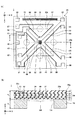
図1は、第1の実施の形態に係る流量センサを例示する図であり、図1(a)は平面透視図、図1(b)は図1(a)のA−A線に沿う断面図である。
<First Embodiment>
[Structure of flow sensor]
FIG. 1 is a diagram illustrating a flow sensor according to a first embodiment. FIG. 1A is a perspective plan view, and FIG. 1B is a cross-section taken along line AA in FIG. FIG.
図1を参照するに、第1の実施の形態に係る流量センサ1は、半導体基板10と、ダイヤフラム部20と、X軸温度検出体30及び31と、Y軸温度検出体32及び33と、発熱抵抗体40と、測温抵抗体50と、配線60〜69と、ダミー配線70及び71と、パッド80〜89(ボンディングパッド)とを有する。
Referring to FIG. 1, a
流量センサ1は、発熱抵抗体40を発熱させた状態で、夫々の温度検出体(X軸温度検出体30及び31、Y軸温度検出体32及び33)の温度検出結果に基づいて、温度検出体上を流れる流体の流量を検出するセンサである。但し、流量センサ1は、流向や流速も検出可能である。流量センサ1は、例えば、空調機器の流量制御や、自動車のエンジン内の空気の流量制御等に用いることができる。
The
半導体基板10は、開口部10xを備えた枠状(額縁状)に形成されている。半導体基板10としては、例えば、シリコン基板(Si基板)やSOI(Silicon on Insulator)基板等を用いることができる。
The
ダイヤフラム部20は、絶縁膜21〜25が順次積層された構造であり、開口部10xを塞ぐように半導体基板10上に設けられている。ダイヤフラム部20の平面形状は、例えば、正方形である。ダイヤフラム部20において、半導体基板10と接していない領域(開口部10xを塞いでいる領域)を特に薄膜構造体部20tと称する。薄膜構造体部20tの平面形状は、例えば、正方形である。薄膜構造体部20tは、半導体基板10と接していないため熱容量が小さく、温度が上昇し易い構造とされている。
The
なお、図1では、ダイヤフラム部20の上面20aの4つの縁辺20eの1つに平行な軸をX軸、ダイヤフラム部20の上面20aと平行な面内でX軸と直交する軸をY軸、ダイヤフラム部20の厚さ方向をZ軸としている。X軸、Y軸、及びZ軸は、互いに直交している。ここで、平面視とは、対象物をダイヤフラム部20の上面20aの法線方向から視ることをいう。又、平面形状とは、対象物をダイヤフラム部20の上面20aの法線方向から視たときの形状をいう。
In FIG. 1, an axis parallel to one of the four
図1(b)では、便宜上、半導体基板10の厚さT1とダイヤフラム部20の厚さT2とを同程度に描いているが、実際には、半導体基板10の厚さT1は比較的厚く、ダイヤフラム部20の厚さT2は比較的薄い。半導体基板10の厚さT1は、例えば、50〜300μm程度とすることができる。又、ダイヤフラム部20の厚さT2は、例えば、0.5〜5μm程度とすることができる。
In FIG. 1 (b), for convenience, is drawn to a thickness T 1 and the same level and a thickness T 2 of the
なお、流量センサ1を基板上に固定して使用する場合があるが、この場合に流量センサ1の側壁(主に半導体基板10の側壁)に流体がぶつかると乱流が発生し、流量が正確に検出できないおそれがある。この観点から、半導体基板10の厚さT1は薄い方が好ましい。半導体基板10の厚さT1を薄くすることにより、基板との間に生じる段差を小さくすることが可能となり、乱流の発生を抑制できる。
In some cases, the
ダイヤフラム部20において、絶縁膜22上には、X軸温度検出体30及び31、並びにY軸温度検出体32及び33が設けられている。X軸温度検出体30及び31並びにY軸温度検出体32及び33は、保護膜として機能する絶縁膜23に被覆されている。絶縁膜23上には、発熱抵抗体40及び測温抵抗体50が、例えばつづら状に形成されている。なお、発熱抵抗体40及び測温抵抗体50をつづら状に形成するのは、発熱抵抗体40及び測温抵抗体50の抵抗値を大きくするためである。発熱抵抗体40及び測温抵抗体50は、保護膜として機能する絶縁膜24に被覆されている。
In the
絶縁膜24上には、配線60〜69、ダミー配線70及び71、並びにパッド80〜89が設けられている。配線60〜69中の所定の配線と、発熱抵抗体40、X軸温度検出体30及び31、Y軸温度検出体32及び33、並びに測温抵抗体50とは、絶縁膜23及び24に形成された垂直配線(図示せず)を介して接続されている。配線60〜69、ダミー配線70及び71、並びにパッド80〜89は、保護膜として機能する絶縁膜25に被覆されている。但し、パッド80〜89の上面の少なくとも一部は、絶縁膜25に設けられた開口部25x内に露出し、流量センサ1の外部との接続を可能としている。
On the
X軸温度検出体30及び31は、X軸に平行な線上に形成されている。Y軸温度検出体32及び33は、Y軸に平行な線上に形成されている。X軸温度検出体30及び31はX軸方向の温度変化を検出する部分であり、Y軸温度検出体32及び33はY軸方向の温度変化を検出する部分である。X軸温度検出体30及び31、並びにY軸温度検出体32及び33は、例えば、酸化バナジウムから形成することができる。
The
X軸温度検出体30の一端は配線62を介してパッド83と接続され、他端は配線63を介してパッド82と接続されている。又、X軸温度検出体31の一端は配線64を介してパッド84と接続され、他端は配線65を介してパッド85と接続されている。
One end of the
パッド82とパッド84は、流量センサ1の外部で接続される。又、パッド83は流量センサ1の外部でGND(又は電源)と接続され、パッド85は流量センサ1の外部で電源(又はGND)と接続される。これにより、X軸温度検出体30とX軸温度検出体31とがGNDと電源との間に直列に接続され、パッド82とパッド84との接続部から中間電位を得ることができる。
The
Y軸温度検出体32の一端は配線67を介してパッド87と接続され、他端は配線66を介してパッド86と接続されている。又、パッド86は配線69を介してY軸温度検出体33の一端と接続され、Y軸温度検出体33の他端は配線68を介してパッド88と接続されている。つまり、Y軸温度検出体32とY軸温度検出体33とは、配線66及び69を介して直列に接続されている。
One end of the Y-
パッド87は流量センサ1の外部でGND(又は電源)と接続され、パッド88は流量センサ1の外部で電源(又はGND)と接続される。これにより、Y軸温度検出体32とY軸温度検出体33とがGNDと電源との間に直列に接続され、パッド86から中間電位を得ることができる。
The
発熱抵抗体40の一端は配線60を介してパッド80に接続され、他端は配線61を介してパッド81に接続されている。パッド80とパッド81との間に電圧を印加すると発熱抵抗体40に電流が流れて発熱する。
One end of the
なお、発熱抵抗体40の材料と配線60及び61の材料に異種材料を使用し、発熱抵抗体40の比抵抗が配線60及び61の比抵抗より大きくなる材料を選択すると好適である。これにより、発熱抵抗体40に電力が集中し、発熱抵抗体40の温度上昇が大きくなるため、上流の温度検出体と下流の温度検出体の検出する温度差が大きくなり、流量の検出感度を向上することができる。
It is preferable to use different materials for the material of the
発熱抵抗体40は、例えば、白金(Pt)、ニクロム(NiCr)、ポリシリコン(p−Si)等から形成することができる。この場合、配線60及び61の材料として、これらより比抵抗の小さいアルミニウム(Al)や金(Au)等を用いることが好ましい。
The
測温抵抗体50の一端はパッド80に接続され、他端はパッド89に接続されている。測温抵抗体50は、パッド80及び89を介して、流量センサ1の外部の抵抗ブリッジ回路に接続され、ブリッジを構成する抵抗の1つとなる。この回路構成により、測温抵抗体50の抵抗変化に基づいて、流体の温度を検出することができる。測温抵抗体50は、例えば、白金(Pt)、ニクロム(NiCr)、ポリシリコン(p−Si)等から形成することができる。
One end of the
[薄膜構造体部における、各温度検出体、発熱抵抗体、配線のレイアウト]
ここで、薄膜構造体部20tにおける、X軸温度検出体30及び31、Y軸温度検出体32及び33、発熱抵抗体40、配線60〜69、並びにダミー配線70及び71のレイアウトの特徴について説明する。
[Layout of each temperature detector, heating resistor, and wiring in the thin film structure]
Here, the layout characteristics of the
薄膜構造体部20tにおいて、平面視において、X軸温度検出体30及び31、Y軸温度検出体32及び33、及び配線60〜69、ダミー配線70及び71は、発熱抵抗体40に対して点対称に配置されている。言い換えれば、薄膜構造体部20t内の各要素を点対称とするために、ダミー配線70及び71を設けたともいえる。
In the thin
なお、ここでいう点対称は、完全に点対称である場合のみではなく、流量の検出感度向上という本発明の効果を損なわない範囲内で略点対称な場合も含むものとする。直交、平行、中心、正方形、円形、対角線上等の文言についても同様である。 Note that the point symmetry here includes not only the case of complete point symmetry but also the case of substantially point symmetry within a range that does not impair the effect of the present invention of improving flow rate detection sensitivity. The same applies to words such as orthogonal, parallel, center, square, circular, and diagonal.
具体的には、発熱抵抗体40は、ダイヤフラム部20の中心(薄膜構造体部20tの中心)に配置されている。又、X軸温度検出体30及び31、Y軸温度検出体32及び33は、発熱抵抗体40の周囲に均等に配置されている。つまり、X軸温度検出体30及び31、Y軸温度検出体32及び33は、発熱抵抗体40から等距離に配置されている。又、発熱抵抗体40を挟んで互いに対向するX軸温度検出体30及び31はX軸と平行な方向に配置されている。又、発熱抵抗体40を挟んで互いに対向するY軸温度検出体32及び33はY軸と平行な方向に配置されている。
Specifically, the
又、発熱抵抗体40の一端から引き出された配線60及び他端から引き出された配線61は、ダイヤフラム部20の1つの対角線上に配置されている。
The
そして、X軸温度検出体30から引き出された配線63と、Y軸温度検出体33から引き出された配線69は、発熱抵抗体40から引き出された配線61の両側に、配線61と平行に配置されている。配線61と配線63との間隔と、配線61と配線69との間隔は、略同一である。
The
同様に、X軸温度検出体31から引き出された配線64と、Y軸温度検出体32から引き出された配線67は、発熱抵抗体40から引き出された配線60の両側に、配線60と平行に配置されている。配線60と配線64との間隔と、配線60と配線67との間隔は、略同一である。
Similarly, the
又、ダイヤフラム部20の他の1つの対角線上において、発熱抵抗体40の両側にダミー配線70及び71が配置されている。
On another diagonal line of the
そして、X軸温度検出体30から引き出された配線62と、Y軸温度検出体32から引き出された配線66は、ダミー配線70の両側に、ダミー配線70と平行に配置されている。ダミー配線70と配線62との間隔と、ダミー配線70と配線66との間隔は、略同一である。
The
同様に、X軸温度検出体31から引き出された配線65と、Y軸温度検出体33から引き出された配線68は、ダミー配線71の両側に、ダミー配線71と平行に配置されている。ダミー配線71と配線65との間隔と、ダミー配線71と配線68との間隔は、略同一である。
Similarly, the
なお、発熱抵抗体40の一端及び他端から引き出された配線を発熱抵抗体配線、各温度検出体から引き出された配線を温度検出体配線と称する場合がある。
Note that the wiring drawn from one end and the other end of the
このように、配線60、64、及び67と、配線61、63、及び69とがダイヤフラム部20の1つの対角線上に配置され、配線70、62、及び66と、配線71、65、及び68とがダイヤフラム部20の他の1つの対角線上に配置されている。
As described above, the
これらの配線を対角線上に配置する理由は、流体はX軸上とY軸上を主に流れるが、配線上を流体が流れたときに、配線から発熱抵抗体の熱が放熱し難くするためである。言い換えれば、配線の方向をX軸又はY軸(流体の流れる方向)に平行にすると、配線上を流体が流れ、配線から発熱抵抗体の熱が放熱してしまうので、配線が延びる方向が流体の流れ(X軸上、Y軸上)と一致しないようにしている。 The reason for arranging these wires on the diagonal line is that the fluid mainly flows on the X axis and the Y axis, but when the fluid flows on the wires, it is difficult for the heat of the heating resistor to radiate from the wires. It is. In other words, if the direction of the wiring is parallel to the X-axis or the Y-axis (the direction in which the fluid flows), the fluid flows on the wiring and the heat of the heating resistor is radiated from the wiring. (On the X-axis and Y-axis).
薄膜構造体部20tへの熱応力は、薄膜構造体部20tの各縁辺(半導体基板10の上面内縁部と接する部分)の中央部を含む4つの領域(図1の4つの応力集中部B)に集中することが確認されている。
The thermal stress on the
そこで、流量センサ1において、配線60〜69、並びにダミー配線70及び71は、4つの応力集中部Bを除く領域に配置されている。前述のように、配線を対角線上に配置しているので、応力集中部Bを避けて配置することが容易となる。
Therefore, in the
薄膜構造体部20t上の配線の幅は、応力緩和のため、薄膜構造体部20tの周囲(半導体基板10上)の配線よりも細く、1〜10μm程度である。配線幅の細い薄膜構造体部20t上の配線を、応力集中部Bを避けて配置することにより、熱応力により断線するおそれを低減できる。
The width of the wiring on the thin
[流量センサの動作]
次に、流量センサ1の動作について説明する。ここでは、流量センサ1は所定の制御回路に接続されているものとする。制御回路は、測温抵抗体50の抵抗変化に基づいて流体の温度を検出して発熱抵抗体40の好適な発熱量を算出し、それに基づいた電圧をパッド80とパッド81との間に印加して発熱抵抗体40に電流を流して発熱させることができる。
[Operation of flow sensor]
Next, the operation of the
又、制御回路との接続により、前述のように、X軸温度検出体30とX軸温度検出体31とがGNDと電源との間に直列に接続され、パッド82とパッド84との接続部から中間電位(中間電位Xとする)を得ることができる。又、Y軸温度検出体32とY軸温度検出体33とがGNDと電源との間に直列に接続されパッド86から中間電位(中間電位Yとする)を得ることができる。
Further, by connecting to the control circuit, as described above, the
発熱抵抗体40に電流を流して発熱させると、薄膜構造体部20tの温度が上昇する。このとき、検知対象となる流体(例えば、空気やガス等)が流れていない場合には、X軸温度検出体30とX軸温度検出体31の出力がバランスしているため、中間電位XとしてGNDと電源の中間の電位(初期値X0とする)が得られる。同様に、Y軸温度検出体32とY軸温度検出体33の出力がバランスしているため、中間電位YとしてGNDと電源の中間の電位(初期値Y0とする)が得られる。
When a current is applied to the
一方、流量センサ1の表面側(ダイヤフラム部20の上面20a側)を流体が流れている場合には、流量センサ1の表面側に温度分布が生じる(上流側が下流側よりも低温となる)。そのため、上流側に配置された温度検出体の抵抗値と、下流側に配置された温度検出体の抵抗値とのバランスが崩れ、中間電位X及びYが変化する。
On the other hand, when the fluid is flowing on the surface side of the flow sensor 1 (the
制御回路は、中間電位X及びYが初期値X0及びY0に対してGND側か電源側の何れの方向に変化したかにより、流体の流れている方向を360°検出することができる。又、制御回路は、中間電位X及びYが初期値X0及びY0に対してどれだけ変化したかにより、流量を測定することができる。なお、中間電位X及びYが変化した方向や変化した量と、流向や流量との関係は、例えば、テーブルとして制御回路内に記憶しておくことができる。 The control circuit can detect the flowing direction of the fluid at 360 ° depending on whether the intermediate potentials X and Y have changed to the GND side or the power supply side with respect to the initial values X 0 and Y 0 . Further, the control circuit can measure the flow rate based on how much the intermediate potentials X and Y have changed with respect to the initial values X 0 and Y 0 . The relationship between the direction in which the intermediate potentials X and Y have changed and the amount of change and the flow direction and the flow rate can be stored in the control circuit as a table, for example.
[流量センサの製造方法]
次に、流量センサ1の製造方法について説明する。図2及び図3は、流量センサの製造工程を例示する図である。図2及び図3では、図1(b)に対応する断面を示しているため、流量センサ1の構成要素の一部は図示されない。
[Production method of flow sensor]
Next, a method for manufacturing the
まず、図2(a)に示す工程では、シリコン基板等からなる半導体基板10を準備し、半導体基板10の上面に、絶縁膜21及び22を順次積層する。絶縁膜21の材料としては、例えば、シリコン酸化膜(SiO2)等を用いることができる。絶縁膜22の材料としては、例えば、シリコン窒化膜(Si3N4)等を用いることができる。絶縁膜21及び22は、例えば、熱酸化法や低温CVD(chemical vapor deposition)法等により形成することができる。
First, in the step shown in FIG. 2A, a
次に、図2(b)に示す工程では、絶縁膜22の上面に、X軸温度検出体30及び31、並びにY軸温度検出体32及び33を形成する。X軸温度検出体30及び31、並びにY軸温度検出体32及び33の材料としては、例えば、酸化バナジウム等を用いることができる。X軸温度検出体30及び31、並びにY軸温度検出体32及び33は、例えば、ゾルゲル法等により形成することができる。
Next, in the step shown in FIG. 2B,
ゾルゲル法を用いる場合には、まず、温度検出体となるソルゲル液(前駆体液)を作製し、絶縁膜22の上面全面にスピンコートにより塗布膜を形成する。次に、塗布膜を加熱して溶媒を蒸発させて乾燥させ固体膜とする。次に、固体膜の不要な部分をエッチングで除去してX軸温度検出体30及び31、並びにY軸温度検出体32及び33を形成する。
When using the sol-gel method, first, a sol-gel liquid (precursor liquid) serving as a temperature detector is prepared, and a coating film is formed on the entire upper surface of the insulating
このように、ゾルゲル法ではスピンコートにより塗布膜を形成するので、塗布膜を形成する面が平坦であることが好ましい。従って、X軸温度検出体30及び31、並びにY軸温度検出体32及び33は、発熱抵抗体40や配線62等よりも下層に形成することが好ましい。仮に、各温度検出体よりも下層に発熱抵抗体40等があると、その上に絶縁膜を形成したとしても絶縁膜の表面に凹凸が残り平坦性が低くなるため、スピンコートを行う面としては好ましくない。
As described above, since the coating film is formed by spin coating in the sol-gel method, the surface on which the coating film is formed is preferably flat. Therefore, it is preferable that the
次に、図2(c)に示す工程では、絶縁膜22の上面に、X軸温度検出体30及び31、並びにY軸温度検出体32及び33を被覆するように、絶縁膜23を形成する。絶縁膜23の材料としては、例えば、シリコン酸化膜(SiO2)等を用いることができる。絶縁膜23は、例えば、スパッタリング法やプラズマCVD法等により形成することができる。
Next, in the step shown in FIG. 2C, the insulating
次に、図2(d)に示す工程では、絶縁膜23の上面に、発熱抵抗体40及び測温抵抗体50を形成する。発熱抵抗体40及び測温抵抗体50の材料としては、例えば、白金(Pt)、ニクロム(NiCr)、ポリシリコン(p−Si)等を用いることができる。発熱抵抗体40及び測温抵抗体50は、例えば、スパッタリング法等により形成することができる。
Next, in the step shown in FIG. 2D, the
次に、図3(a)に示す工程では、絶縁膜23の上面に、発熱抵抗体40及び測温抵抗体50を被覆するように、絶縁膜24を形成する。絶縁膜24の材料としては、例えば、シリコン酸化膜(SiO2)等を用いることができる。絶縁膜24は、例えば、スパッタリング法やプラズマCVD法等により形成することができる。
Next, in the step shown in FIG. 3A, the insulating
次に、図3(b)に示す工程では、絶縁膜24の上面に、配線60〜69、ダミー配線70及び71、並びにパッド80〜89を形成する。配線60〜69、ダミー配線70及び71、並びにパッド80〜89の材料としては、例えば、アルミニウム(Al)や金(Au)等を用いることができる。配線60〜69、ダミー配線70及び71、並びにパッド80〜89は、例えば、スパッタリング法等により形成することができる。なお、配線60〜69を下層の発熱抵抗体40等に接続する部分には、絶縁膜をエッチングしてコンタクトホールを形成し、コンタクトホール内にアルミニウム(Al)や金(Au)等からなる垂直配線を形成する。
Next, in the step shown in FIG. 3B, wirings 60 to 69, dummy wirings 70 and 71, and
次に、図3(c)に示す工程では、絶縁膜24の上面に、配線60〜69、ダミー配線70及び71、並びにパッド80〜89を被覆するように、絶縁膜25を形成する。絶縁膜25の材料としては、例えば、シリコン酸化膜(SiO2)やシリコン窒化膜(Si3N4)等を用いることができる。絶縁膜25は、例えば、スパッタリング法やプラズマCVD法等により形成することができる。その後、パッド80〜89の夫々の上面の少なくとも一部が絶縁膜25から露出するように、ドライエッチング等により開口部25xを形成する。
Next, in the step shown in FIG. 3C, the insulating
次に、図3(d)に示す工程では、半導体基板10の中央部に開口部10xを形成する。これにより、開口部10x内に絶縁膜21の下面が露出し、薄膜構造体部20tができあがる。開口部10xは、例えば、DRIEにより形成できる。開口部10xは、水酸化テトラメチルアンモニウム(TMAH)や水酸化カリウム(KOH)等をエッチング液に用いたウェットエッチングにより形成してもよい。以上の工程により、図1に示す流量センサ1が完成する。
Next, in a step shown in FIG. 3D, an
なお、以上は単独の流量センサ1を作製する工程として説明したが、半導体ウェハ上に流量センサ1となる複数の領域を形成し、その後ダイシング等により個片化して複数の流量センサ1を同時に形成する工程とすると効率的である。
Although the above description has been given as a step of fabricating a
このように、第1の実施の形態に係る流量センサ1では、薄膜構造体部20tにおいて、平面視において、X軸温度検出体30及び31、Y軸温度検出体32及び33、及び配線60〜69、ダミー配線70及び71を、発熱抵抗体40に対して点対称に配置している。これにより、発熱抵抗体40からの熱が薄膜構造体部20tに均等に伝わり、流体の流れる向き(流向)に対して温度分布のばらつきが少なくなるため、流量の検出感度を向上することができる。
As described above, in the
又、発熱抵抗体配線と温度検出体配線とを互いに平行に配置することにより、発熱抵抗体40から発生した熱が薄膜構造体部20t上に分布しやすくなり、上流の温度検出体と下流の温度検出体の検出する温度差が大きくなる。これにより、流量の検出感度を向上することができる。
Further, by arranging the heating resistor wiring and the temperature detector wiring in parallel with each other, the heat generated from the
又、発熱抵抗体40の材料と発熱抵抗体配線(配線60及び61)の材料に異種材料を使用し、発熱抵抗体40の比抵抗が発熱抵抗体配線の比抵抗より大きくなる材料を選択することにより、発熱抵抗体40に電力が集中し、発熱抵抗体40の温度上昇が大きくなる。そのため、上流の温度検出体と下流の温度検出体の検出する温度差が大きくなり、流量の検出感度を向上することができる。
Further, different materials are used for the material of the
薄膜構造体部20tの応力集中部Bに配線を配置しないことにより、薄膜構造体部20tへの熱応力による影響が緩和され、配線と薄膜構造体部の機械的強度を向上することができる。
By not arranging the wiring in the stress concentration portion B of the thin
又、各温度検出体に酸化バナジウムを用いることにより、流量の検出感度を向上することができると共に、発熱抵抗体の低消費電力化及び温度検出体の小型化が可能となる。 Further, by using vanadium oxide for each temperature detector, the detection sensitivity of the flow rate can be improved, the power consumption of the heating resistor can be reduced, and the size of the temperature detector can be reduced.
〈第1の実施の形態の変形例1〉
第1の実施の形態の変形例1では、薄膜構造体部にスリットを設ける例を示す。なお、第1の実施の形態の変形例1において、既に説明した実施の形態と同一構成部についての説明は省略する場合がある。
<Modification Example 1 of First Embodiment>
In the first modification of the first embodiment, an example is shown in which a slit is provided in the thin film structure. In the first modification of the first embodiment, the description of the same components as those of the embodiment described above may be omitted.
図4は、第1の実施の形態の変形例1に係る流量センサを例示する平面透視図である。図4に示すように、流量センサ2は、薄膜構造体部20tに、8本のスリット20xが設けられた点が、流量センサ1(図1参照)と相違する。スリット20xの平面形状は、例えば、細長状(例えば、長方形や楕円形等)とすることができる。
FIG. 4 is a perspective plan view illustrating a flow sensor according to Modification Example 1 of the first embodiment. As shown in FIG. 4, the
具体的には、スリット20xは、配線60と、配線60の両側に配線60と平行に配置された配線64及び67との間に設けられている。又、配線61と、配線61の両側に配線61と平行に配置された配線63及び69との間に設けられている。
Specifically, the
同様に、ダミー配線70と、ダミー配線70の両側にダミー配線70と平行に配置された配線62及び66との間に設けられている。又、ダミー配線71と、ダミー配線71の両側にダミー配線71と平行に配置された配線65及び68との間に設けられている。
Similarly, the
このように、薄膜構造体部20tにスリット20xを設けることにより、薄膜構造体部20tの熱容量を低減することができる。これにより、発熱抵抗体40の温度上昇が大きくなるため、上流の温度検出体と下流の温度検出体の検出する温度差が大きくなり、流量の検出感度を更に向上することができる。なお、スリットは、薄膜構造体部20tの他の部分に対称に設けてもよい。
As described above, by providing the
〈第1の実施の形態の変形例2〉
第1の実施の形態の変形例2では、薄膜構造体部の平面形状を変えた例を示す。なお、第1の実施の形態の変形例2において、既に説明した実施の形態と同一構成部についての説明は省略する場合がある。
<Modified Example 2 of First Embodiment>
図5は、第1の実施の形態の変形例2に係る流量センサを例示する平面透視図である。図5に示すように、流量センサ3は、薄膜構造体部20tが薄膜構造体部20uに置換された点が、流量センサ1(図1参照)と相違する。
FIG. 5 is a perspective plan view illustrating a flow sensor according to
流量センサ3では、半導体基板10の開口部10xの平面形状が円形である。その結果、薄膜構造体部20uの平面形状も円形である。なお、薄膜構造体部20uは、平面形状が円形になった以外は薄膜構造体部20tと同様である。
In the
このように、円形の薄膜構造体部20uを設けることにより、応力集中部Bがなくなるため、配線と薄膜構造体部の機械的強度を更に向上することができる。
By providing the circular thin
〈第1の実施の形態の変形例3〉
第1の実施の形態の変形例3では、1軸の流量センサの例を示す。なお、第1の実施の形態の変形例3において、既に説明した実施の形態と同一構成部についての説明は省略する場合がある。
<Third Modification of First Embodiment>
In a third modification of the first embodiment, an example of a uniaxial flow sensor will be described. In the third modification of the first embodiment, the description of the same components as those of the embodiment described above may be omitted.
図6は、第1の実施の形態の変形例3に係る流量センサを例示する平面透視図である。図6に示すように、流量センサ4は、Y軸温度検出体32及び33のみが配置され、X軸温度検出体が配置されていない点が、流量センサ1(図1参照)と相違する。流量センサ4では、Y軸方向のみの流量を検出することができる。このように、1軸の流量センサを実現することも可能である。
FIG. 6 is a perspective plan view illustrating a flow sensor according to
以上、本発明の好ましい実施の形態について詳説したが、本発明は、上述した実施の形態に制限されることはなく、本発明の範囲を逸脱することなく、上述した実施の形態に種々の変形及び置換を加えることができる。 As described above, the preferred embodiments of the present invention have been described in detail. However, the present invention is not limited to the above-described embodiments, and various modifications may be made to the above-described embodiments without departing from the scope of the present invention. And substitutions can be added.
1、2、3、4 流量センサ
10 半導体基板
10x、25x 開口部
20 ダイヤフラム部
20a ダイヤフラム部の上面
20e ダイヤフラム部の縁辺
20t、20u 薄膜構造体部
20x スリット
21〜25 絶縁膜
30、31 X軸温度検出体
32、33 Y軸温度検出体
40 発熱抵抗体
50 測温抵抗体
60〜69 配線
70、71 ダミー配線
80〜89 パッド
1, 2, 3, 4
Claims (9)
開口部を備えた枠状の半導体基板と、
前記半導体基板上に設けられたダイヤフラム部と、
前記ダイヤフラム部に設けられた発熱抵抗体及び複数の温度検出体と、を有し、
複数の前記温度検出体は酸化バナジウムから形成されたゾルゲル膜であり、
前記ダイヤフラム部は、前記開口部を塞ぐ薄膜構造体部を備え、
平面視において、前記薄膜構造体部には、前記発熱抵抗体の周囲に複数の前記温度検出体が配置されており、
前記薄膜構造体部は、複数の絶縁膜を含む多層構造を有し、前記温度検出体は、第1の絶縁膜上に形成され、前記発熱抵抗体は、前記第1の絶縁膜よりも上層の第2の絶縁膜上に形成されることを特徴とする流量センサ。 A heating resistor and a plurality of temperature detectors are provided, and in a state where the heating resistors are heated, a flow rate of a fluid flowing on the temperature detector is detected based on a temperature detection result of each of the temperature detectors. A flow sensor,
A frame-shaped semiconductor substrate having an opening;
A diaphragm portion provided on the semiconductor substrate,
A heating resistor and a plurality of temperature detectors provided in the diaphragm portion,
The plurality of temperature detectors are sol-gel films formed from vanadium oxide,
The diaphragm portion includes a thin film structure that closes the opening,
In a plan view, in the thin film structure portion, a plurality of the temperature detectors are arranged around the heating resistor,
The thin film structure section has a multilayer structure including a plurality of insulating films, the temperature detector is formed on a first insulating film, and the heating resistor is formed above the first insulating film. A flow sensor formed on the second insulating film.
前記発熱抵抗体は、前記ダイヤフラム部の中心に配置され、
前記ダイヤフラム部の4つの縁辺の1つに平行な軸をX軸、前記ダイヤフラム部の上面と平行な面内でX軸と直交する軸をY軸としたときに、互いに対向する2つの前記温度検出体は前記X軸と平行な方向に配置され、互いに対向する他の2つの前記温度検出体は前記Y軸と平行な方向に配置されていることを特徴とする請求項4に記載の流量センサ。 The planar shape of the diaphragm portion is a square,
The heating resistor is disposed at the center of the diaphragm,
When the axis parallel to one of the four edges of the diaphragm portion is the X axis, and the axis orthogonal to the X axis in a plane parallel to the upper surface of the diaphragm portion is the Y axis, the two temperatures opposed to each other. 5. The flow rate according to claim 4 , wherein the detector is disposed in a direction parallel to the X axis, and the other two temperature detectors facing each other are disposed in a direction parallel to the Y axis. 6. Sensor.
前記発熱抵抗体の一端及び他端から引き出された発熱抵抗体配線は、前記ダイヤフラム部の1つの対角線上に配置されていることを特徴とする請求項5に記載の流量センサ。 In the thin film structure,
The flow sensor according to claim 5 , wherein the heating resistor wires drawn from one end and the other end of the heating resistor are arranged on one diagonal line of the diaphragm section.
前記ダイヤフラム部の他の1つの対角線上において、前記発熱抵抗体の両側にダミー配線が配置されており、
前記温度検出体配線は、前記ダミー配線の両側に前記ダミー配線と平行に配置された配線を含むことを特徴とする請求項6に記載の流量センサ。 In the thin film structure,
On another diagonal line of the diaphragm, dummy wirings are arranged on both sides of the heating resistor,
7. The flow sensor according to claim 6 , wherein the temperature detector wiring includes wiring arranged on both sides of the dummy wiring in parallel with the dummy wiring.
Priority Applications (5)
| Application Number | Priority Date | Filing Date | Title |
|---|---|---|---|
| JP2015194417A JP6669957B2 (en) | 2015-09-30 | 2015-09-30 | Flow sensor |
| US15/759,570 US10739176B2 (en) | 2015-09-30 | 2016-09-23 | Flow rate sensor having temperature detectors and heat element provided on different insulator layers of diaphragm part |
| EP16851350.5A EP3339816A4 (en) | 2015-09-30 | 2016-09-23 | Flow rate sensor |
| PCT/JP2016/077980 WO2017057176A1 (en) | 2015-09-30 | 2016-09-23 | Flow rate sensor |
| CN201680052519.1A CN108027267B (en) | 2015-09-30 | 2016-09-23 | Flow sensor |
Applications Claiming Priority (1)
| Application Number | Priority Date | Filing Date | Title |
|---|---|---|---|
| JP2015194417A JP6669957B2 (en) | 2015-09-30 | 2015-09-30 | Flow sensor |
Related Child Applications (1)
| Application Number | Title | Priority Date | Filing Date |
|---|---|---|---|
| JP2019234495A Division JP6807005B2 (en) | 2019-12-25 | 2019-12-25 | Flow sensor |
Publications (2)
| Publication Number | Publication Date |
|---|---|
| JP2017067643A JP2017067643A (en) | 2017-04-06 |
| JP6669957B2 true JP6669957B2 (en) | 2020-03-18 |
Family
ID=58423697
Family Applications (1)
| Application Number | Title | Priority Date | Filing Date |
|---|---|---|---|
| JP2015194417A Active JP6669957B2 (en) | 2015-09-30 | 2015-09-30 | Flow sensor |
Country Status (5)
| Country | Link |
|---|---|
| US (1) | US10739176B2 (en) |
| EP (1) | EP3339816A4 (en) |
| JP (1) | JP6669957B2 (en) |
| CN (1) | CN108027267B (en) |
| WO (1) | WO2017057176A1 (en) |
Cited By (1)
| Publication number | Priority date | Publication date | Assignee | Title |
|---|---|---|---|---|
| JP2020143903A (en) * | 2019-03-04 | 2020-09-10 | ミネベアミツミ株式会社 | Fluid sensor |
Families Citing this family (5)
| Publication number | Priority date | Publication date | Assignee | Title |
|---|---|---|---|---|
| US11402253B2 (en) * | 2018-06-26 | 2022-08-02 | Minebea Mitsumi Inc. | Fluid sensing apparatus and method for detecting failure of fluid sensor |
| JP6905962B2 (en) * | 2018-07-12 | 2021-07-21 | 日立Astemo株式会社 | Flow sensor |
| CN109211342B (en) * | 2018-09-05 | 2020-03-20 | 四方光电股份有限公司 | Airflow flowmeter, MEMS silicon-based temperature-sensitive chip and preparation method thereof |
| JP2021131323A (en) * | 2020-02-20 | 2021-09-09 | サーパス工業株式会社 | Flowmeter and flowmeter manufacturing method |
| WO2024143146A1 (en) * | 2022-12-29 | 2024-07-04 | TopoLogic株式会社 | Measuring device and measuring unit |
Family Cites Families (23)
| Publication number | Priority date | Publication date | Assignee | Title |
|---|---|---|---|---|
| JPH0810231B2 (en) | 1987-03-31 | 1996-01-31 | シャープ株式会社 | Flow sensor |
| JP2976924B2 (en) * | 1997-05-19 | 1999-11-10 | 日本電気株式会社 | Thin film temperature-sensitive resistance material and method of manufacturing the same |
| JP3067737B2 (en) | 1998-05-18 | 2000-07-24 | 日本電気株式会社 | Plasma etching method for vanadium oxide film |
| JP3513041B2 (en) * | 1999-01-25 | 2004-03-31 | 三菱電機株式会社 | Flow sensor |
| US6626037B1 (en) * | 1999-09-03 | 2003-09-30 | Denso Corporation | Thermal flow sensor having improved sensing range |
| US7473031B2 (en) * | 2002-04-01 | 2009-01-06 | Palo Alto Research Center, Incorporated | Resistive thermal sensing |
| JP2004061412A (en) * | 2002-07-31 | 2004-02-26 | Horiba Ltd | Fluid sensor |
| TW574128B (en) * | 2002-11-29 | 2004-02-01 | Lightuning Tech Inc | Thermal bubble type micro-machined inertial sensor |
| JP4380196B2 (en) * | 2003-03-26 | 2009-12-09 | 株式会社デンソー | Sensor device |
| DE60331692D1 (en) | 2003-10-02 | 2010-04-22 | Honeywell Int Inc | METHOD FOR PRODUCING THERMAL DETECTOR STRUCTURES |
| JP4609019B2 (en) * | 2004-09-24 | 2011-01-12 | 株式会社デンソー | Thermal flow sensor and manufacturing method thereof |
| JP2006162423A (en) * | 2004-12-07 | 2006-06-22 | Mitsuteru Kimura | Flow sensor |
| JP2006258678A (en) * | 2005-03-18 | 2006-09-28 | Hitachi Ltd | Thermal flow meter |
| JP4966526B2 (en) * | 2005-09-07 | 2012-07-04 | 日立オートモティブシステムズ株式会社 | Flow sensor |
| JP2008026205A (en) * | 2006-07-24 | 2008-02-07 | Hitachi Ltd | Thermal gas flow sensor and apparatus for controlling internal combustion engine using the same |
| JP2008170382A (en) | 2007-01-15 | 2008-07-24 | Hitachi Ltd | Thermal fluid flow sensor, and manufacturing method therefor |
| JP5141482B2 (en) * | 2008-09-30 | 2013-02-13 | 株式会社デンソー | Flow sensor |
| JP5315304B2 (en) * | 2010-07-30 | 2013-10-16 | 日立オートモティブシステムズ株式会社 | Thermal flow meter |
| JP5683192B2 (en) * | 2010-09-30 | 2015-03-11 | 日立オートモティブシステムズ株式会社 | Thermal flow sensor |
| US8356514B2 (en) * | 2011-01-13 | 2013-01-22 | Honeywell International Inc. | Sensor with improved thermal stability |
| WO2012172528A1 (en) * | 2011-06-17 | 2012-12-20 | Universidade Do Minho | 3 axis polymeric accelerometer and method of production |
| JP5982398B2 (en) * | 2011-11-28 | 2016-08-31 | 日立オートモティブシステムズ株式会社 | Thermal air flow sensor |
| US10128302B2 (en) * | 2016-01-28 | 2018-11-13 | Ams Sensors Uk Limited | IR detector array device |
-
2015
- 2015-09-30 JP JP2015194417A patent/JP6669957B2/en active Active
-
2016
- 2016-09-23 US US15/759,570 patent/US10739176B2/en active Active
- 2016-09-23 CN CN201680052519.1A patent/CN108027267B/en active Active
- 2016-09-23 EP EP16851350.5A patent/EP3339816A4/en not_active Withdrawn
- 2016-09-23 WO PCT/JP2016/077980 patent/WO2017057176A1/en unknown
Cited By (2)
| Publication number | Priority date | Publication date | Assignee | Title |
|---|---|---|---|---|
| JP2020143903A (en) * | 2019-03-04 | 2020-09-10 | ミネベアミツミ株式会社 | Fluid sensor |
| JP7235218B2 (en) | 2019-03-04 | 2023-03-08 | ミネベアミツミ株式会社 | fluid sensor |
Also Published As
| Publication number | Publication date |
|---|---|
| EP3339816A1 (en) | 2018-06-27 |
| JP2017067643A (en) | 2017-04-06 |
| US20190154484A1 (en) | 2019-05-23 |
| EP3339816A4 (en) | 2018-10-17 |
| CN108027267B (en) | 2020-08-04 |
| US10739176B2 (en) | 2020-08-11 |
| WO2017057176A1 (en) | 2017-04-06 |
| CN108027267A (en) | 2018-05-11 |
Similar Documents
| Publication | Publication Date | Title |
|---|---|---|
| JP6669957B2 (en) | Flow sensor | |
| US11073415B2 (en) | Thermal fluid flow sensor having a dielectric membrane comprising discontinuities between the heating element and an edge | |
| JP5683192B2 (en) | Thermal flow sensor | |
| JP5315304B2 (en) | Thermal flow meter | |
| JPH1123338A (en) | Thermosensitive flow-rate detecting element and flow-rate sensor using the same | |
| US12078519B2 (en) | Thermopile-based flow sensing device | |
| US20200284633A1 (en) | Fluid sensor | |
| JP2012078246A (en) | Electric element, integrated element and electronic circuit | |
| JP6807005B2 (en) | Flow sensor | |
| JP4798961B2 (en) | HEATER DEVICE AND GAS SENSOR DEVICE USING THE SAME | |
| JP5492834B2 (en) | Thermal flow meter | |
| JP5765609B2 (en) | Electrical device, integrated device, electronic circuit and temperature calibration device | |
| JP2011209038A (en) | Flow sensor | |
| JP6951225B2 (en) | Humidity sensor | |
| Zhu et al. | A self-packaged two-dimensional thermal wind sensor based on thermopiles for low cost applications | |
| WO2017203860A1 (en) | Humidity measuring apparatus | |
| JP2000146656A (en) | Flow sensor and manufacture thereof | |
| JPH11344369A (en) | Flow-rate detecting element and flow-rate sensor | |
| JP2003106884A (en) | Airflow sensor | |
| JP2001153704A (en) | Flow sensor | |
| JPH10260069A (en) | Manufacture of flow rate detecting element | |
| JP2003106883A (en) | Airflow sensor | |
| JP2021179377A (en) | Thermal type flowmeter | |
| JP2004077428A (en) | Pressure sensor | |
| JPH04295767A (en) | Fluid detector |
Legal Events
| Date | Code | Title | Description |
|---|---|---|---|
| A621 | Written request for application examination |
Free format text: JAPANESE INTERMEDIATE CODE: A621 Effective date: 20180827 |
|
| A131 | Notification of reasons for refusal |
Free format text: JAPANESE INTERMEDIATE CODE: A131 Effective date: 20190402 |
|
| A521 | Written amendment |
Free format text: JAPANESE INTERMEDIATE CODE: A523 Effective date: 20190531 |
|
| A131 | Notification of reasons for refusal |
Free format text: JAPANESE INTERMEDIATE CODE: A131 Effective date: 20190723 |
|
| A521 | Written amendment |
Free format text: JAPANESE INTERMEDIATE CODE: A523 Effective date: 20190919 |
|
| A02 | Decision of refusal |
Free format text: JAPANESE INTERMEDIATE CODE: A02 Effective date: 20191029 |
|
| A521 | Written amendment |
Free format text: JAPANESE INTERMEDIATE CODE: A523 Effective date: 20191225 |
|
| A911 | Transfer of reconsideration by examiner before appeal (zenchi) |
Free format text: JAPANESE INTERMEDIATE CODE: A911 Effective date: 20200108 |
|
| TRDD | Decision of grant or rejection written | ||
| A01 | Written decision to grant a patent or to grant a registration (utility model) |
Free format text: JAPANESE INTERMEDIATE CODE: A01 Effective date: 20200128 |
|
| A61 | First payment of annual fees (during grant procedure) |
Free format text: JAPANESE INTERMEDIATE CODE: A61 Effective date: 20200210 |
|
| R150 | Certificate of patent or registration of utility model |
Ref document number: 6669957 Country of ref document: JP Free format text: JAPANESE INTERMEDIATE CODE: R150 |