JP6667133B2 - Image forming apparatus and image forming system - Google Patents
Image forming apparatus and image forming system Download PDFInfo
- Publication number
- JP6667133B2 JP6667133B2 JP2015233586A JP2015233586A JP6667133B2 JP 6667133 B2 JP6667133 B2 JP 6667133B2 JP 2015233586 A JP2015233586 A JP 2015233586A JP 2015233586 A JP2015233586 A JP 2015233586A JP 6667133 B2 JP6667133 B2 JP 6667133B2
- Authority
- JP
- Japan
- Prior art keywords
- charging
- image
- toner
- charging bias
- latent image
- Prior art date
- Legal status (The legal status is an assumption and is not a legal conclusion. Google has not performed a legal analysis and makes no representation as to the accuracy of the status listed.)
- Active
Links
Images


Description
本発明は、画像形成装置、並びに、管理装置及びこれと通信可能な複数の画像形成装置とを備える画像形成システムに関するものである。 The present invention relates to an image forming apparatus, an image forming system including a management apparatus, and a plurality of image forming apparatuses that can communicate with the management apparatus.
従来より、潜像担持体の表面に形成した地汚れパターンのトナー付着量を検知した結果に基づいて、帯電電源からの帯電バイアスの出力値を所定の上限調整量の範囲内で調整する帯電バイアス調整制御を実施する画像形成装置が知られている。 Conventionally, a charging bias that adjusts an output value of a charging bias from a charging power supply within a range of a predetermined upper limit adjustment amount based on a result of detecting a toner adhesion amount of a background stain pattern formed on a surface of a latent image carrier. 2. Related Art An image forming apparatus that performs adjustment control is known.
例えば、特許文献1に記載の画像形成装置は、次のような帯電バイアス調整処理を実施するようになっている。即ち、潜像担持体たる感光体を回転させ且つ静電潜像の書き込みを行わない状態で、感光体を帯電させる帯電装置に供給する帯電バイアスを段階的に変化させる。そして、感光体におけるそれぞれの帯電バイアスの条件で帯電させた領域を現像装置との対向位置に順に通していくことで、感光体表面に地汚れパターンを形成する。次いで、その地汚れパターンにおけるそれぞれの領域のトナー付着量をトナー付着量検知センサーによって検知した結果に基づいて、帯電バイアスの値と地汚れ量との関係を特定し、特定結果に基づいて、地汚れを生じない値に帯電バイアスを調整する。
For example, the image forming apparatus described in
この画像形成装置によれば、帯電バイアス調整処理を定期的に実施することで、環境の変化、帯電部材の電気抵抗の経時変化、及び感光体表面層の厚み変化にかかわらず、感光体の地肌部の電位を適切な値に維持して地汚れの発生を抑えることができる。 According to this image forming apparatus, the charging bias adjustment process is periodically performed, so that the background of the photoconductor is not affected regardless of changes in the environment, changes in the electrical resistance of the charging member over time, and changes in the thickness of the photoconductor surface layer. The occurrence of background contamination can be suppressed by maintaining the potential of the portion at an appropriate value.
しかしながら、帯電バイアス調整処理において帯電バイアスの調整量を大きくし過ぎると、調整前後で細線の太さを大きく変化させたり、中間調部の画像濃度を大きく変化させたり、二次色や三次色の色味を大きく変化させたりしてしまうことがわかった。 However, if the adjustment amount of the charging bias is excessively increased in the charging bias adjustment process, the thickness of the thin line is largely changed before and after the adjustment, the image density of the halftone portion is largely changed, or the secondary color or the tertiary color is changed. It was found that the color changed greatly.
上述した課題を解決するために、請求項1の発明は、潜像担持体と、前記潜像担持体の表面を帯電させる帯電手段と、前記帯電手段に供給する帯電バイアスを出力する帯電電源と、帯電後の前記表面に静電潜像を書き込む潜像書込手段と、前記静電潜像を現像してトナー像を得る現像手段と、トナー像を前記表面から転写体に転写する転写手段と、前記潜像担持体又は前記転写体の表面におけるトナー付着量を検知するトナー付着量検知手段と、地肌ポテンシャルを段階的に変化させながら前記潜像担持体の表面に地汚れパターンを形成し、前記地汚れパターンのトナー付着量を前記トナー付着量検知手段によって検知した結果に基づいて、前記帯電電源からの帯電バイアスの出力値を所定の上限調整量の範囲内で調整する帯電バイアス調整制御を実施する制御手段とを備える画像形成装置であって、前記上限調整量が、面積階調によってベタ部よりも画像濃度を低減された面積階調部の色差△Eを所定値以下にする値に設定され、前記所定値が10であることを特徴とするものである。
In order to solve the above-described problem, the invention according to
本発明によれば、帯電バイアス調整処理による帯電バイアスの調整前後における細線の太さの変化、中間調部の画像濃度の変化、及び色味の変化を何れも目立たないレベルまで低減することができるという優れた効果がある。 According to the present invention, a change in the thickness of a thin line, a change in image density in a halftone portion, and a change in color before and after the adjustment of the charging bias by the charging bias adjustment process can be reduced to a level that is inconspicuous. There is an excellent effect.
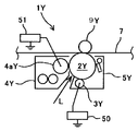
以下、本発明を適用した画像形成装置の実施形態の一例として、電子写真方式のプリンタについて説明する。まず、本プリンタの基本的な構成について説明する。図1は、本プリンタの構成を示す概略構成図である。図1に示されるように、このプリンタは、イエロー(Y),シアン(C),マゼンタ(M),黒(K)の各色の画像を形成するための4つの画像形成ユニット1Y,1C,1M,1Kを備えている。以下、各符号の添字Y,C,M,Kは、それぞれイエロー、シアン、マゼンタ、黒用の部材であることを示す。Y,C,M,Kの色順は、図1に示される順に限られるものでなく、他の並び順であっても構わない。
Hereinafter, an electrophotographic printer will be described as an example of an embodiment of an image forming apparatus to which the present invention is applied. First, the basic configuration of the printer will be described. FIG. 1 is a schematic configuration diagram showing the configuration of the present printer. As shown in FIG. 1, this printer has four
図2は、本プリンタの画像形成ユニットの構成を示す構成図である。図2に示されるように、画像形成ユニット1Yに備えられた潜像担持体たるドラム状の感光体2Yの周囲には、帯電手段たる帯電ローラ3Y、現像手段たる現像装置4Y、クリーニング装置5Yなどが配設されている。ゴムローラからなる帯電ローラ3Yは、感光体2Yの表面に接触しながら回転するようになっている。本プリンタでは、かかる帯電ローラ3Yに対して、帯電バイアスとして、AC成分を含まないDCバイアスを印加する接触DC帯電方式を採用している。なお、帯電ローラ3Yには、接触AC帯電ローラ方式や非接触帯電ローラ方式などの他の方式を採用することもできる。
FIG. 2 is a configuration diagram illustrating a configuration of an image forming unit of the printer. As shown in FIG. 2, around a drum-shaped
現像装置4Y内には、イエロートナーと磁性キャリアとを含有する二成分現像剤が収容されている。この二成分現像剤は、平均粒径4.9〜5.5μmのトナーと、ブリッジ抵抗が12.1[LogΩ・cm]以下である小粒径・低抵抗キャリアとを含有するものである。現像装置4Yは、感光体2に対向した現像部材たる現像ローラ4aY、現像剤を搬送・撹拌するスクリュー、トナー濃度センサー等から構成される。現像ローラ4aYは、中空で回転自在なスリーブと、これに連れ回らないように内包されるマグネットローラとから構成されている。
The developing
画像形成ユニット1Yでは、感光体2Yと、その周囲に配設される帯電ローラ3Y、現像装置4Y、クリーニング装置5Yとが1つのユニットとして共通の支持体に支持されるプロセスカートリッジとして構成されている。これにより、画像形成ユニット1Yは、プリンタ本体に対して着脱可能になっており、その寿命到達持に一度に消耗部品を交換できるようになっている。他の画像形成ユニット1C,1M,1Kは、トナーとしてシアントナー、マゼンタトナー、黒トナーを用いるが、それ以外の構成は、Y用の画像形成ユニットと同様である。
In the
画像形成ユニット1Y,1C,1M,1Kの下方には、潜像書込手段たる光書込ユニット6が配置されている。光書込ユニット6は、光源、ポリゴンミラー、f−θレンズ、反射ミラー等を備え、画像データに基づいて各色の感光体2Y,2C,2M,2Kの表面に対してレーザー光Lの光走査を行う。この光走査により、感光体2Y,2C,2M,2K上に、複数のドットからなるデジタル画像又はドットパターンの前駆体となるイエロー,シアン,マゼンタ,黒用の静電潜像が形成される。
Below the
画像形成ユニット1Y,1C,1M,1Kの上方には、各色のトナー像を各色の感光体(2Y,2C,2M,2K)から中間転写ベルト7を介して記録シートSに転写する中間転写ユニット8が配置されている。中間転写ベルト7は、複数のローラに張架されながら、少なくともいずれか1つのローラの回転駆動によって図中反時計回り方向に無端移動せしめられる。中間転写ユニット8は、中間転写ベルト7の他、一次転写ローラ9Y,9C,9M,9K、ブラシローラやクリーニングブレードなどから構成されるクリーニング装置10、二次転写バックアップローラ11、光学センサーユニット20などを備えている。
Above the
一次転写ローラ9Y,9C,9M,9Kは、中間転写ベルト7を各色の感光体との間に挟み込んでいる。これにより、感光体2Y,2M,2C,2Kと、中間転写ベルト7のおもて面とが当接するY,M,C,K用の一次転写ニップが形成されている。中間転写ユニット8は、画像形成ユニット1Kよりもベルト移動方向下流側で、二次転写バックアップローラ11の近傍にてベルトループ外側に位置する二次転写ローラ12を備えている。二次転写ローラ12は、二次転写バックアップローラ11との間に中間転写ベルト7挟み込んで二次転写ニップを形成している。
The
二次転写ローラ12の上方には、定着ユニット13が配設されている。定着ユニット13は、互いに回転しながら当接して定着ニップを形成する定着ローラと加圧ローラとを備えている。定着ローラは、ハロゲンヒータを内蔵し、定着ローラ表面が所定の温度となるように、電源からのヒータへ電力が供給され、加圧ローラとの間に定着ニップを形成している。
Above the
プリンタ本体の下部には、出力画像が記録される記録媒体たる記録シートSを複数枚重ねて収容する給紙カセット14a、14b、給紙ローラ、レジストローラ対15などが配設されている。また、プリンタ本体の側面には、側面から手差しで給紙を行うための手差しトレイ14cが備えられている。また、中間転写ユニット8や定着ユニット13の図中右側には、両面印刷時に記録シートSを再び二次転写ニップへ搬送するための両面ユニット16が設けられている。
At the lower part of the printer main body, paper feed cassettes 14a and 14b for accommodating a plurality of recording sheets S as recording media on which an output image is recorded, a paper feed roller, a
プリンタ本体の上部には、画像形成ユニット1Y,1C,1M,1Kの現像装置へトナーを補給するトナー補給容器17Y、17C、17M、17Kが配設されている。また、プリンタ本体には、制御手段たる制御部30、廃トナーボトル、電源ユニットなども設けられている。
At the top of the printer body,
次に、プリンタの動作について説明する。まず、帯電ローラ3Yの帯電ローラに電源より所定の電圧が印加されて、対向する感光体2Y表面が帯電せしめられる。所定の電位に帯電した感光体2Yの表面には、光書込ユニット6によって画像データに基づくレーザー光Lの走査がなされ、これによって感光体2Yに静電潜像が書き込まれる。静電潜像を担持した感光体2Yの表面が感光体2Yの回転に伴って現像装置4Yに到達すると、感光体2Yと対向配置される現像ローラ4aYにより、感光体2Yの表面の静電潜像にYトナーが供給される。これにより、感光体2Yの表面にYトナー像が形成される。現像装置3Y内には、トナー濃度センサーの出力に応じて、トナー補給容器17Yから適量のYトナーが補給される。
Next, the operation of the printer will be described. First, a predetermined voltage is applied from a power supply to the charging roller of the charging
同様の動作が画像形成ユニット1C,M,Kにおいても所定のタイミングで行われる。これにより、感光体2Y,2C,2M,2Kの表面に、Y,C,M,Kトナー像が形成される。これらY,C,M,Kトナー像は、Y,C,M,K用の一次転写ニップで中間転写ベルト7のおもて面に順に重ね合わせて一次転写されていく。この一次転写は、一次転写ローラ9Y,9C,9M,9Kに、一次転写電源から出力されるトナーと逆極性の一次転写バイアスが印加されることで行われる。
Similar operations are performed at predetermined timings in the
実施形態に係るプリンタでは、一次転写ローラ9Y,9C,9M,9Kや一次転写電源が、Y,C,M,Kトナー像を潜像担持体たる感光体2Y,2C,2M,2Kの表面から転写体たる中間転写ベルト7に転写する転写手段として機能している。中間転写ベルト方式に代えて、次のような搬送ベルト方式を採用した場合であっても、一次転写ローラや一次転写電源が転写手段として機能する。即ち、無端状の搬送ベルトを感光体と一次転写ローラとの間に挟み込んで形成した一次転写ニップに、搬送ベルトの表面に保持した記録シートSを進入させて、感光体上のトナー像を記録シートSに直接転写する方式である。かかる構成においては、感光体上に形成したテストトナー像を記録シートSではなく、転写体たる搬送ベルトの表面に転写した後、ベルト表面上のテストトナー像のトナー付着量を検知することが可能である。
In the printer according to the embodiment, the
記録シートSは、給紙カセット14a、14b、もしくは手差しトレイ14cのいずれかから搬送され、レジストローラ対15に到達したところで一旦停止する。そして、所定のタイミングに合わせてレジストローラ対15が回転して記録シートSを二次転写ニップへ向けて送り出す。
The recording sheet S is conveyed from one of the paper feed cassettes 14a and 14b or the manual feed tray 14c, and temporarily stops when it reaches the
中間転写ベルト7上に重ね合わされたY,C,M,Kトナー像は、二次転写ローラ12と中間転写ベルト7とが当接する二次転写ニップで記録シートSに二次転写される。この二次転写は、二次転写電源によって二次転写ローラ12にトナーと逆極性の電圧が印加されることで行われる。
The Y, C, M, and K toner images superimposed on the
記録シートSは、二次転写ニップを出た後に定着ユニット13に向けて搬送されて定着ニップに挟み込まれる。記録シートS上のトナー像は、定着ニップにて定着ローラからの熱により加熱定着される。トナー像が定着せしめられた記録シートSは、片面印刷の場合には、各搬送ローラによって機外に排出される。また、両面印刷の場合、記録シートSは、各搬送ローラによって両面ユニット16へ搬送されて反転され、先に画像が形成された面とは反対側の面に、上述したように画像が形成された後に機外に排出される。
After leaving the secondary transfer nip, the recording sheet S is conveyed toward the fixing
本プリンタにおいては、環境変動や経時における画像品質の安定化を図るために、所定のタイミングでプロセスコントロールと呼ばれる制御を実施する。プロセスコントロール処理では、感光体2Yに複数のパッチ状Yトナー像からなるYパッチパターン像を現像し、それを中間転写ベルト7に転写する。また、感光体2C,2M,2Kにも、同様にしてC,M,Kパッチパターン像を形成する。そして、それらのパッチパターン像における各トナー像のトナー付着量を、トナー付着量検知手段たる光学センサーユニット20で検出し、その検出結果に基づいて現像バイアスVbなどの作像条件を調整する。
In the present printer, control called process control is performed at a predetermined timing in order to stabilize image quality over environmental changes and aging. In the process control process, a Y patch pattern image composed of a plurality of patch Y toner images is developed on the
図3は、本プリンタの電気回路の要部を示すブロック図である。また、図4は、プロセスコントロールにおける演算処理の流れを示すフローチャートである。図3に示されるように、制御部30には、画像形成ユニット1Y,1C,1M,1K、光書込ユニット6、給紙モータ81、レジストモータ82、中間転写ユニット8、光学センサーユニット20、入力装置53などが電気的に接続されている。この制御部30は、演算処理や各種プログラムを実行するCPU30aと、データを記憶するRAM30bとを備えている。なお、給紙モータ81は、各給紙カセットや給紙トレイの給紙ローラの駆動源になっている。また、レジストモータ82は、レジストローラの駆動源になっている。
FIG. 3 is a block diagram showing a main part of an electric circuit of the printer. FIG. 4 is a flowchart showing the flow of arithmetic processing in process control. As shown in FIG. 3, the
光学センサーユニット20は、中間転写ベルト7のベルト幅方向に所定の間隔をおいて並ぶ複数の反射型フォトセンサーを有している。それぞれの反射型フォトセンサーは、中間転写ベルト7や中間転写ベルト7上の後述するパッチ状トナー像の光反射率に応じた信号を出力するように構成されている。この反射型フォトセンサーは、4つ設けられている。そのうちの3つは、Y,M,Cトナー像やY,C,M付着トナーに応じた出力を行えるように、ベルト表面上における正反射光及び拡散反射光の両方をとらえて、それぞれの光量に応じた出力を行う。残りの1つは、Kトナー像やK付着トナーに応じた出力を行うように、ベルト表面上における正反射光だけをとらえてその光量に応じた出力を行う。
The
制御部30は、主電源の投入時や、所定時間経過した後の待機時、所定枚数以上のプリントを出力したあとの待機時など、所定のタイミングで、プロセスコントロール処理を実施する。具体的には、この所定のタイミングが到来すると、まず、図4に示されるように、通紙枚数、印字率、温度、湿度などの環境情報を取得する(ステップS1)。次に、画像形成ユニット1Y,1C,1M,1Kにおけるそれぞれの現像特性を把握する。具体的には、それぞれの色について、現像ガンマγと現像開始電圧を算出する(ステップS2)。具体的には、次のように行う。即ち、感光体2Y,2C,2M,2Kを回転させながらそれぞれを一様に帯電せしめる。この帯電については、帯電バイアスVcとして通常のプリント時における一様な値(例えば−700V)とは異なり、その絶対値を段階的に大きくしていく。光書込ユニット6によるレーザー光Lの走査によって感光体2Y,2C,2M,2Kに、パッチ状Yトナー像,パッチ状Cトナー像、パッチ状Mトナー像、パッチ状Kトナー像用の静電潜像を形成する。このときのレーザー光量は露光による感光体電位の減衰量を飽和させるのに十分な光量に設定されている。それらの静電潜像を現像装置12Y,12C,12M,12Kによって現像することで、感光体2Y,2C,2M,2K上にY,C,M,Kパッチパターン像を形成する。なお、現像の際に、制御部30は、各色の現像ローラ(4a)に印加する現像バイアスVbの絶対値も前述した帯電電位に合わせて段階的に徐々に大きくしていく。これらの異なる現像バイアスVbに応じて感光体上には異なる付着量のトナーパターンが現像される。現像バイアスVb、帯電バイアスVcは、何れも負極性のDCバイアスからなる。
The
Y,C,M,Kパッチパターン像は、図5に示されるように、中間転写ベルト7上に重なり合わずに、ベルト幅方向に並ぶように転写される。具体的には、Yパッチパターン像YPPは、中間転写ベルト7の幅方向における一端部に転写される。また、Cパッチパターン像CPPは、ベルト幅方向において、Yパッチパターン像よりも少し中央側にずれた位置に転写される。また、Mパッチパターン像MPPは、中間転写ベルト7の幅方向における他端部に転写される。また、Kパッチパターン像KPPは、ベルト幅方向において、Kパッチパターン像よりも少し中央側にずれた位置に転写される。
As shown in FIG. 5, the Y, C, M, and K patch pattern images are transferred on the
光学センサーユニット20は、互いにベルト幅方向の異なる位置でベルトの光反射特性を検知する第1反射型フォトセンサー20a、第2反射型フォトセンサー20b、第3反射型フォトセンサー20c、及び第4反射型フォトセンサー20dを有している。これら4つの反射型フォトセンサーのうち、第3反射型フォトセンサー20cは、黒トナーの付着に起因するベルト表面の光反射特性の変化を検知するように、正反射光だけを検知するものを採用している。これに対し、その他の反射型フォトセンサーは、Y,C又はMトナーの付着に起因するベルト表面の光反射特性の変化を検知するように、正反射光と拡散反射光との両方を検知するタイプのものである。
The
第1反射型フォトセンサー20aは、中間転写ベルト7の幅方向の一端部に形成されたYパッチパターン像YPPのパッチ状Yトナー像のYトナー付着量を検知する位置に配設されている。また、第2反射型フォトセンサー20bは、ベルト幅方向において、Yパッチパターン像YPPの近くに位置するCパッチパターン像CPPのパッチ状Cトナー像のCトナー付着量を検知する位置に配設されている。また、第4反射型フォトセンサー20dは、中間転写ベルト7の幅方向の他端部に形成されたMパッチパターン像MPPのパッチ状Mトナー像のMトナー付着量を検知する位置に配設されている。また、第3反射型フォトセンサー20cは、ベルト幅方向において、Mパッチパターン像MPPの近くに位置するKパッチパターン像KPPのパッチ状Kトナー像のKトナー付着量を検知する位置に配設されている。なお、第1反射型フォトセンサー20a、第2反射フォトセンサー20b、及び第4反射型フォトセンサー20dの3つは、それぞれトナー像の色が黒以外の3色(Y,C,M)であれば、そのトナー付着量を検知することができる。
The first
制御部30は、光学センサーユニット20の4つの反射型フォトセンサーから順次送られてくる出力信号に基づいて、各色のパッチ状トナー像の光反射率を演算し、演算結果に基づいてトナー付着量を求めてRAM30aに格納していく。なお、中間転写ベルト7の走行に伴って光学センサーユニット20との対向位置を通過した各色のパッチパターン像は、クリーニング装置10によってベルトおもて面からクリーニングされる。
The
次に、RAM30aに格納した画像濃度データ(トナー付着量)と、別途RAM150bに格納されている露光部電位(潜像電位)とパターン作像に用いた現像バイアスとの差分である現像ポテンシャルのデータとから、直線近似式を算出する。図6に示される直線近似式(Y=a×(Vl−Vb)+b)である。同図の2次元座標において、x軸は、露光部電位Vlから、そのときに印加した現像バイアスVbを減じた値、即ち、現像ポテンシャル(Vl−Vb)を示している。Y軸は、単位面積当たりのトナー付着量(y)を示す。図6には、パッチ状トナー像の数に対応した数だけ、X−Y平面上にデータがプロットされる。そのプロットされた複数のデータに基づいて、直線近似をおこなうX−Y平面上の区間を決定する。その後、その区間内で、最小自乗法をおこなって直線近似式(y=a×Vb+b)を得る。このとき直線近似式に基づいて、現像ガンマγと現像開始電圧Vkとが算出される。現像ガンマγは直線近似式の傾きとして算出され(γ=a)、現像開始電圧Vkは直線近似式とX軸との交点として算出される(Vk=−b/a)。こうして、各色の画像形成ユニット1Y,1C,1M,1Kの現像特性が算出される(ステップS2)。
Next, development potential data, which is the difference between the image density data (toner adhesion amount) stored in the
次に、求めた現像特性に基づいて、帯電電位(地肌部電位)Vdの目標値(目標帯電電位)と、露光部電位Vlと、現像バイアスVbとが求められる(ステップ3)。具体的には、現像バイアスVbは、次のようにして求められる。即ち、現像ガンマγと現像開始電圧Vkとの組み合わせによって最大トナー付着量を得るための現像ポテンシャルを求める。そして、その現像ポテンシャルを得ることができる現像バイアスVbを前回のプロセスコントロール実施時の露光部電位Vlに基づいて求める。次に、その現像バイアスVbと予め設定された地肌ポテンシャルとに基づいて、目標帯電電位を求める。 Next, a target value (target charging potential) of the charging potential (background portion potential) Vd, an exposure portion potential Vl, and a developing bias Vb are obtained based on the obtained development characteristics (step 3). Specifically, the developing bias Vb is obtained as follows. That is, the developing potential for obtaining the maximum toner adhesion amount is determined by the combination of the developing gamma γ and the developing start voltage Vk. Then, a developing bias Vb at which the developing potential can be obtained is obtained based on the exposed portion potential Vl at the time of the previous process control. Next, a target charging potential is obtained based on the developing bias Vb and a preset background potential.
このようにして目標帯電電位が求められると、予めの実験結果に基づいて構築されてRAM中にルックアップテーブルを利用して、目標帯電電位に対応する露光部電位Vlが特定される。露光部電位は帯電電位が大きく変化しても、あまり変化しない。前回のプロセスコントロール実施時に求められた露光部電位Vlと今回新たに求められた露光部電位Vlとの差が所定値以内であれば、帯電電位Vd、露光部電位Vl、現像バイアスVbの決定が終了される。 When the target charging potential is obtained in this way, the exposure unit potential Vl corresponding to the target charging potential is specified by using a look-up table in the RAM, which is constructed based on the result of a previous experiment. The exposed portion potential does not change much even if the charging potential changes significantly. If the difference between the exposed portion potential Vl obtained during the previous process control and the newly obtained exposed portion potential Vl is within a predetermined value, the charging potential Vd, the exposed portion potential Vl, and the developing bias Vb are determined. Will be terminated.
露光部電位Vlの変化が所定値以上であれば、現像バイアスVbを新たな露光部電位Vlに基づいて再計算され、帯電電位Vdも再計算される。そして、帯電電位Vd、露光部電位Vl、現像バイアスVbの決定が終了される。現像ローラの現像スリーブの表面は、現像バイアスVbとほぼ同じ値になることから、感光体の表面が目標帯電電位に帯電し、適切に露光していれば、狙いの現像ポテンシャルや地肌ポテンシャルを得ることができる。 If the change in the exposed portion potential Vl is equal to or greater than a predetermined value, the developing bias Vb is recalculated based on the new exposed portion potential Vl, and the charging potential Vd is also recalculated. Then, the determination of the charging potential Vd, the exposure portion potential Vl, and the developing bias Vb is completed. Since the surface of the developing sleeve of the developing roller has almost the same value as the developing bias Vb, the surface of the photoreceptor is charged to the target charging potential, and if the surface is properly exposed, the desired developing potential and background potential are obtained. be able to.
制御部30は、次に、帯電バイアスVcを決定する。具体的には、目標帯電電位が得られる帯電バイアスVcは、感光体表面層の摩耗量や、環境に影響される帯電ローラの電気抵抗などに応じて変化する。そこで、制御部30は、環境(温湿度)及び感光体走行距離、その走行距離における平均印字率の組み合わせから、目標帯電電位を得ることが可能な帯電バイアスVcを求めるためのアルゴリズムを記憶している。このアルゴリズムは、予めの実験に基づいて構築されたものである。そして、環境センサー52による温湿度の検知結果、及びRAMに記憶している感光体走行距離、平均印字率の組み合わせにより、目標帯電電位を得ることが可能な帯電バイアスVcを、アルゴリズムを用いて求める。
Next, the
現像剤の性質として、地汚れは初期に比べて経時の方が悪く、逆にキャリア付着(エッジキャリア付着)は経時に比べて初期の方が悪い状態である。そのため、現像剤の使用に伴って、最適な地肌ポテンシャルは大きな値の方にシフトする。また一般的に、高温高湿環境では、トナーの帯電量が低いために地汚れが悪化し、逆に低温低湿環境では、キャリア付着が不利になる。このため、本実施形態に係る画像濃度制御においては、地肌ポテンシャルを初期/経時+環境で最適な値にシフトさせる。 As a property of the developer, background contamination is worse as time passes than in the initial stage, and carrier adhesion (edge carrier adhesion) is worse in the initial stage as compared to the initial period. Therefore, with the use of the developer, the optimal background potential shifts toward a larger value. In general, in a high-temperature and high-humidity environment, the amount of toner charge is low, so that background fouling worsens. In a low-temperature and low-humidity environment, carrier adhesion is disadvantageous. For this reason, in the image density control according to the present embodiment, the background potential is shifted to an optimum value in the initial / time + environment.
既に実験によって地肌汚れとキャリア付着を目標以下にするのに最適な地肌ポテンシャルは各条件において求められている。このため、帯電ローラやキャリアの劣化及び温湿度の変化などの環境情報があれば、ある程度の補正は可能である。しかし、実験時との誤差や予想外の因子により最適な地肌ポテンシャルが変動する可能性がある。一方、現像開始電圧Vkは感光体2上への現像が開始される電圧として考えることができるので、現像開始電圧Vkの絶対値と同等以上の地肌ポテンシャルがないと地汚れが悪くなると考えられる。
Optimum background potential for making the background contamination and carrier adhesion below the target has already been obtained by experiments under various conditions. For this reason, if there is environmental information such as deterioration of the charging roller and carrier and changes in temperature and humidity, it is possible to make some corrections. However, the optimal background potential may fluctuate due to errors from the experiment and unexpected factors. On the other hand, since the development start voltage Vk can be considered as a voltage at which development on the
そこで、制御部30は、図4に示されるように、ステップS3の工程後に、狙いの現像開始電圧Vk'を決定する(ステップS4)。狙いの現像開始電圧Vk'はあらかじめ実験により環境情報と紐付けされテーブル化されており、最初に取得した環境情報からテーブルを参照して狙いの現像開始電圧Vk'を決定する。そして、現像開始電圧Vkと狙いの現像開始電圧Vk'との差分の量で区分を決定する(ステップS5)。例えば、現像開始電圧Vkが狙いの現像開始電圧Vk'に対して+40V以上離れていれば区分1、+40V未満+20V以上で区分2、+20V未満0V以上で区分3というように区分分けする。そして、現像開始電圧Vkがどの区分にあるか特定し、区分毎に補正量を決定する(ステップS6)。次に、ステップS3で求めた帯電電位Vdと現像バイアスVbとから算出される地肌ポテンシャルに対して、ステップS5で決定された補正量を加算して目標地肌ポテンシャルを算出する。そして、この目標地肌ポテンシャルが得られるように帯電バイアスVcを決定する(ステップS7)。
Therefore, as shown in FIG. 4, after the step S3, the
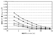
図7は、現像ポテンシャルや地肌ポテンシャルを説明するためのグラフである。図7に示されるように、地肌ポテンシャルは、帯電電位Vdと現像バイアスVbとの差分であり、画像の非画像部(地肌部分)において作用するものである。地肌ポテンシャルが小さいと地汚れが発生し易くなる一方で、地肌ポテンシャルが大きいとキャリア付着が発生し易くなることから、地肌ポテンシャルを適切な値に設定する必要がある。 FIG. 7 is a graph for explaining the development potential and the background potential. As shown in FIG. 7, the background potential is a difference between the charging potential Vd and the developing bias Vb, and acts on a non-image portion (background portion) of an image. If the background potential is small, background contamination is likely to occur, while if the background potential is large, carrier adhesion is likely to occur. Therefore, it is necessary to set the background potential to an appropriate value.
図8は、地肌ポテンシャルと、地汚れやキャリア付着の度合いとの関係の一例を示すグラフである。この例では、プロセスコントロールの実施により、地肌ポテンシャルの理論値が140[V]に設定された例を示している。理論値と表現したのは、次に説明する理由による。即ち、プロセスコントロールにより、適切な帯電電圧Vdと現像バイアスVbとの関係に基づいて地肌ポテンシャルが決定され、それに基づいて帯電バイアスVcが決定されることは既に述べた通りである。しかし、その帯電バイアスVcにより、帯電電位Vdが目標帯電電位になっているとは限らない。これは、帯電ローラと感光体との間の放電開始電圧が、様々な要因によって変化し、それによって同じ帯電電位Vdを得るための帯電バイアスVcが変化するからである。プロセスコントロールでは、帯電バイアスVcを決定するにあたり、環境や感光体走行距離を考慮しているが、あくまでも理論的なアルゴリズムによるものであるので、その通りになるとは限らない。また、同じ帯電電位Vdを得るための帯電バイアスVcの値は、環境や感光体走行距離とは異なる他のパラメータによって変化する。 FIG. 8 is a graph showing an example of the relationship between the background potential and the degree of background contamination or carrier adhesion. This example shows an example in which the theoretical value of the background potential is set to 140 [V] by performing the process control. The reason why it is expressed as a theoretical value is as follows. That is, as described above, the background potential is determined based on the relationship between the appropriate charging voltage Vd and the developing bias Vb by the process control, and the charging bias Vc is determined based on the background potential. However, the charging potential Vd is not always at the target charging potential due to the charging bias Vc. This is because the discharge starting voltage between the charging roller and the photoconductor changes due to various factors, and thereby the charging bias Vc for obtaining the same charging potential Vd changes. In the process control, the environment and the photoconductor travel distance are taken into consideration in determining the charging bias Vc. However, since it is based on a theoretical algorithm, it is not always the case. Further, the value of the charging bias Vc for obtaining the same charging potential Vd changes depending on the environment and other parameters different from the photoconductor travel distance.
同図に示される例では、地肌ポテンシャルが140[V]になっていれば、地汚れ及びキャリア付着の両方を抑えることができる。そこで、制御部30は、プロセスコントロールの際に、たとえば140[V]の地肌ポテンシャルと、所望の現像ポテンシャルとが得られるように、目標帯電電位を決定している。ところが、帯電電位Vdを得るための帯電バイアスVcの値が様々な要因によって変化してしまうことから、プロセスコントロールによって決定した帯電バイアスVcによってその目標帯電電位が得られているとは限らない。場合によっては、実際の帯電電位Vdが目標帯電電位(図示の例では140V)から大きくずれることもある。すると、同図において、実際の地肌ポテンシャルが170Vを超えてキャリア付着が発生したり、実際の地肌ポテンシャルが110Vを下回って地汚れが発生したりする。
In the example shown in the figure, if the background potential is 140 [V], both background contamination and carrier adhesion can be suppressed. Therefore, the
既に述べたように、ゴムローラからなる帯電ローラ(例えば3Y)には、帯電バイアスVcが印加される。感光体(例えば2Y)の帯電電位Vdは、図9に示されるように、「Vd=a×Vc+b」という式で表される特性を示す。aは図9に示されるグラフの傾きであり、bはグラフにおけるVd軸切片であり、マイナスの値になる。グラフにおけるVc軸切片は、帯電ローラと感光体との間における放電開始電圧とほぼ同じ値になる。また、傾きaは、ほぼ1になる。 As described above, the charging bias Vc is applied to the charging roller (for example, 3Y) formed of a rubber roller. As shown in FIG. 9, the charging potential Vd of the photoreceptor (for example, 2Y) has a characteristic represented by the equation “Vd = a × Vc + b”. a is the slope of the graph shown in FIG. 9, and b is the Vd axis intercept in the graph, which is a negative value. The Vc-axis intercept in the graph is substantially the same value as the discharge starting voltage between the charging roller and the photoconductor. Further, the inclination a becomes substantially 1.
本プリンタにおいては、既に述べたように、感光体に接触させた帯電ローラに対して直流成分だけからなる帯電バイアスを印加する接触DC帯電方式を採用している。接触DC帯電方式では、帯電バイアスとしてAC/DC重畳バイアスを用いる方式とは異なり、AC電源を必要としないことから、低コスト化を図ることができる。その一方で、帯電ローラと感光体との間に交番電界を形成しないことから、帯電バイアスVcの値を同図のグラフに示される放電開始電圧よりも大きくしないと、帯電ローラと感光体との間で放電を生じせしめることができず、感光体を全く帯電させることができない。また、帯電させることができたとしても、放電開始電圧が環境、感光体表面層の摩耗量、帯電ローラの電気抵抗や汚れ量などに応じて変動することから、同じ帯電バイアスVcの条件下では帯電電位Vdが変動してしまう。このため、AC帯電方式に比べて、所望の帯電電位Vdを安定して得ることが難しくなる。 As described above, this printer employs a contact DC charging method in which a charging bias consisting of only a DC component is applied to a charging roller that is in contact with a photoconductor. The contact DC charging method does not require an AC power source, unlike the method using an AC / DC superimposed bias as the charging bias, so that the cost can be reduced. On the other hand, since an alternating electric field is not formed between the charging roller and the photoconductor, unless the value of the charging bias Vc is higher than the discharge starting voltage shown in the graph of FIG. No discharge can be caused between the photoconductors, and the photoconductor cannot be charged at all. Even if the charging can be performed, the discharge starting voltage varies depending on the environment, the wear amount of the photoconductor surface layer, the electric resistance of the charging roller, the amount of dirt, and the like. The charging potential Vd fluctuates. Therefore, it becomes more difficult to stably obtain a desired charging potential Vd as compared with the AC charging method.
図10は、帯電電位Vdと感光体走行距離xとの関係を示すグラフである。感光体走行距離xは、感光体の回転に伴う感光体表面の移動距離の累積値である。図示のように、帯電電位Vdは、「Vd=ex+f」という式で表される特性を示す。eは同グラフの傾きである。fは、グラフのVd軸切片である。傾きeや切片fの値は一定ではなく、経時的にランダムに変化する。これは次に説明する理由による。即ち、感光体の表面には、クリーニングブレードや現像剤などが摺擦することから、感光体表面層は経時的に摩耗していく。この摩耗に伴って、感光体の静電容量は経時的に大きくなっていき、それに伴って放電開始電圧が低下して、帯電電位Vdが上昇していく。また、画像面積、画像の形状(例えば縦帯のように主走査方向に一部分だけ画像が存在する形状:この場合には画像に接触する感光体箇所の摩耗が進む)、環境、キャリア付着量など、多様な因子によって磨耗量が変化する。加えて、帯電ローラの表面のトナーやトナー添加剤による汚れの状況はランダムに変化して、それに応じて放電開始電圧も変化する。これらのことから、傾きeや切片fは経時的にランダムに変化するのである。このような変化があったり、感光体表面層の磨耗量を直接計測することができなかったりすることから、算術的な手法によって帯電
電位Vdを求めることは非常に困難である。
FIG. 10 is a graph showing the relationship between the charging potential Vd and the photoconductor travel distance x. The photoconductor travel distance x is a cumulative value of a moving distance of the photoconductor surface accompanying rotation of the photoconductor. As shown in the drawing, the charging potential Vd shows a characteristic represented by the equation “Vd = ex + f”. e is the slope of the graph. f is the Vd axis intercept of the graph. The values of the slope e and the intercept f are not constant, but change randomly with time. This is for the following reason. That is, the surface of the photoreceptor is rubbed with a cleaning blade, a developer, or the like, so that the surface layer of the photoreceptor wears over time. With the abrasion, the electrostatic capacity of the photoconductor increases with time, and accordingly, the discharge starting voltage decreases and the charging potential Vd increases. In addition, the image area, the shape of the image (for example, a shape in which only a part of the image exists in the main scanning direction such as a vertical band: in this case, the wear of the photosensitive member in contact with the image proceeds), the environment, the amount of carrier adhesion, and the like. The amount of wear varies depending on various factors. In addition, the state of contamination of the surface of the charging roller with the toner or the toner additive changes randomly, and the discharge starting voltage changes accordingly. From these facts, the slope e and the intercept f change randomly with time. Since there is such a change and the amount of wear of the photoconductor surface layer cannot be directly measured, it is very difficult to obtain the charging potential Vd by an arithmetic method.
一方、電子写真プロセスにおいて、安定した画像濃度を得るためには、露光量(潜像の書込光量)を適切に制御する必要がある。露光量が適正値よりも多くなると、ドット径やライン幅が大きくなって、中間調部において画像形状が潰れたようになる。また、適正値よりも少なくなると、ハイライト部が白抜けになることもある。 On the other hand, in the electrophotographic process, in order to obtain a stable image density, it is necessary to appropriately control the exposure amount (the amount of latent image writing). If the exposure amount exceeds the appropriate value, the dot diameter and the line width become large, and the image shape becomes crushed in the halftone portion. If the value is smaller than the appropriate value, the highlight portion may be blank.
図11は、帯電電位Vdと露光量適正値との関係を示すグラフである。感光体の状態が初期状態である場合には、帯電電位Vdは、「Vd=cK+d」という式で表される特性を示す。cはグラフの傾きであり、dはグラフのVd軸切片である。露光量を一定にした場合、所望の画像濃度を得るためには帯電電位Vdを安定化させる必要がある。また、感光体の状態が古くなっていくと、帯電電位Vdと露光量適正値との関係式は、「Vd=c'K+d'」というように変化していく。このため、露光量を一定にしただけでは、所望の画像濃度を維持することはできない。 FIG. 11 is a graph showing the relationship between the charging potential Vd and the appropriate exposure value. When the state of the photoconductor is the initial state, the charging potential Vd shows a characteristic represented by the equation of “Vd = cK + d”. c is the slope of the graph, and d is the Vd axis intercept of the graph. When the exposure amount is fixed, it is necessary to stabilize the charging potential Vd in order to obtain a desired image density. Further, as the state of the photoconductor becomes older, the relational expression between the charging potential Vd and the appropriate exposure value changes as "Vd = c'K + d '". For this reason, a desired image density cannot be maintained only by keeping the exposure amount constant.
図12は、地汚れIDと、地肌ポテンシャルと、エッジキャリア付着(感光体に対するキャリア付着量)との関係を示すグラフである。地汚れIDは、感光体の地肌部のトナーを粘着テープに転写して画像濃度を測定した値である。また、エッジキャリア付着は、エッジ部を強調した領域を多く含む特定の画像を出力した際に、感光体における画像のエッジ付近に付着した磁性キャリアをカウントした値である。図示のように、地肌ポテンシャルが下がると地肌汚れIDが上昇し、この逆に地肌ポテンシャルが上がるとエッジキャリア付着が上昇する。図示の例では、地肌ポテンシャルの適正値が180V程度になっており、地肌ポテンシャルについては適正値の±30V内に留めないと、地肌汚れやキャリア付着が発生してしまう。この適正値は、機種毎によって異なるが、同じ機種であれば、それほど大きく変動しない。 FIG. 12 is a graph showing the relationship between the background stain ID, the background potential, and the edge carrier adhesion (the amount of carrier adhesion to the photoconductor). The background stain ID is a value obtained by transferring the toner on the background of the photoconductor to an adhesive tape and measuring the image density. The edge carrier adhesion is a value obtained by counting the number of magnetic carriers attached near the edge of the image on the photoconductor when a specific image including a large number of regions where the edge portions are emphasized is output. As shown in the drawing, when the background potential decreases, the background contamination ID increases, and conversely, when the background potential increases, the edge carrier adhesion increases. In the illustrated example, the appropriate value of the background potential is about 180 V. If the background potential is not kept within the appropriate value of ± 30 V, background contamination or carrier adhesion occurs. The appropriate value differs for each model, but does not change so much for the same model.
そこで、制御部30は、プロセスコントロールを実施した後、必要に応じて、目標帯電電位が得られるように帯電バイアスVcを調整するための帯電バイアス調整制御を実施するようになっている。
Therefore, after performing the process control, the
図13は、制御部30によって実施される定期ルーチン処理の流れを示すフローチャートである。この定期ルーチン処理において、制御部30は、まず、プロセスコントロールの実行タイミングについて、到来したか否かを判定する(S1)。そして、到来していない場合には(S1でN)、定期ルーチン処理を直ちに終了する。一方、到来した場合には(S1でY)、S2以降のフローを実行する。
FIG. 13 is a flowchart illustrating a flow of a periodic routine process performed by the
S2においては、上述したプロセスコントロールを実施する。なお、プロセスコントロール処理の開始の前に、連続プリント動作を行っている場合には、連続プリント動作を一時中止してから、プロセスコントロールを開始する。 In S2, the above-described process control is performed. If the continuous printing operation is being performed before the start of the process control process, the continuous printing operation is temporarily stopped before starting the process control.
制御部30は、プロセスコントロールを終えると、次に、Y,C,M,Kの各色の現像装置にそれぞれ収容されている現像剤のトナー濃度を調整するトナー濃度調整処理を実施する(S3)。プロセスコントロールにおいては、トナー濃度の目標値を変更することもあることから、プロセスコントロールの後に、トナー濃度を調整するのである。現状のトナー濃度が目標値よりも低い場合には現像剤にトナーを補給し、現状のトナー濃度が目標値よりも高い場合には、必要に応じてトナー消費量のトナー像を現像してトナーを強制消費させる。
After finishing the process control, the
トナー濃度調整処理を終えると、次に、帯電バイアス調整制御の必要性について判断する。具体的には、感光体走行距離がある閾値まで長くなると、プロセスコントロールにおいて求めた目標帯電電位と、実際の帯電電位Vdとのずれが生じ始めることが経験的に解っている。これに対し、感光体走行距離が閾値まで到達していない場合には、前述のずれはそれほど生じないことが経験的に解っている。そこで、制御部30は、感光体走行距離が10km(閾値)未満である場合には(S4でN)、判定用のフラグをOFFにした後に(S8)、S9に進む。そして、フラグセット中でない(=帯電バイアス調整処理の必要なし)と判定して、定期ルーチン処理を終了する。
When the toner density adjustment processing is completed, it is next determined whether charging bias adjustment control is necessary. Specifically, it has been empirically found that when the photoconductor travel distance increases to a certain threshold, a deviation between the target charging potential obtained in the process control and the actual charging potential Vd starts to occur. On the other hand, it has been empirically found that when the photoconductor travel distance has not reached the threshold value, the above-described deviation does not occur so much. Therefore, when the photoconductor travel distance is less than 10 km (threshold) (N in S4), the
感光体走行距離が閾値に達していても、環境によっては、目標帯電電位と実際の帯電電位Vdとのずれ量が比較的小さい値になることも経験的に解っている。具体的には、温度がある閾値以下の場合には、ずれ量が大きくなるので帯電バイアス調整処理の実施が必要になる。また、温度が閾値を超えていても、絶対湿度が低すぎたり高すぎたりする場合には、ずれ量が大きくなるので帯電バイアス調整処理の実施が必要になる。それら以外のケースでは、ずれ量が比較的小さくなるので、帯電バイアス調整処理の必要性は低い。 It has been empirically found that even when the photoconductor travel distance has reached the threshold value, the amount of deviation between the target charging potential and the actual charging potential Vd is relatively small depending on the environment. Specifically, when the temperature is lower than a certain threshold value, the deviation amount increases, so that it is necessary to perform a charging bias adjustment process. Further, even if the temperature exceeds the threshold value, if the absolute humidity is too low or too high, the deviation amount becomes large, so that it is necessary to perform the charging bias adjustment processing. In other cases, the shift amount is relatively small, so that the necessity of the charging bias adjustment process is low.
そこで、制御部30は、感光体走行距離が10kmを超える場合には(S4でY)、次に、10℃(閾値)以下であるか否かを判定する(S5)。そして、10℃以下である場合には(S5でY)、フラグをセットした後に(S7)、上述したS9を経て、帯電バイアス調整制御(S10)を実行する。また、10℃以下でない場合には(S4でN)、絶対湿度について適正範囲内であるか否かを判定する(S6)。例えば、5mg/m3よりも高く且つ18mg/m3よりも低い(適正範囲内)か否かを判定する。そして、そうでない場合には(S6でN)、先に述べたS7、S9を経て帯電バイアス調整制御(S10)を実施する。これに対し、絶対湿度が適正範囲内にある場合には(S6でY)、先に述べたS8、S9を経て、帯電バイアス調整制御を実施することなく定期ルーチン処理を終了する。
Therefore, when the photoconductor travel distance exceeds 10 km (Y in S4), the
このように、感光体走行距離と、環境センサー52による検知結果(温湿度)とに基づいて、帯電バイアス調整制御の実施タイミングを決定することで、不必要な帯電バイアス調整制御の実施を抑えて装置のダウンタイムを低減することができる。なお、帯電バイアス調整制御を実施した場合には、再びトナー濃度調整処理を実施してから、定期ルーチン処理を終えるようにしてもよい。
As described above, by determining the execution timing of the charging bias adjustment control based on the photoconductor travel distance and the detection result (temperature and humidity) by the
帯電バイアス調整制御において、制御部30は、各色についてそれぞれ次のような処理を行って、各色の地汚れパターンを中間転写ベルト7上に形成する。即ち、まず、光書込ユニット6を停止させた状態で感光体を回転駆動させながら、帯電バイアスVcを段階的に変化させて、感光体表面の周方向において帯電電位Vdの異なる複数の区画を形成する。そして、それら区画を感光体の回転に伴って現像位置に通すことで、互いに地汚れ量の異なる複数の区画(互いに異なる地肌ポテンシャルが作用している)からなる地汚れパターンを感光体表面に形成する。そして、この地汚れパターンを中間転写ベルト7に一次転写する。なお、各色の地汚れパターンは、ベルト移動方向において互いに重ならないようにベルトおもて面に一次転写される。
In the charging bias adjustment control, the
図14は、Y用の画像形成ユニット1Yにおける地汚れパターン形成時の各電位の経時変化を示すグラフである。制御部30は、Y地汚れパターンを形成する際に、図示のように、現像バイアスVbを一定の値に維持したまま、帯電バイアスVcを段階的に変化させて、異なる帯電電位Vdのパターンを作っていく。本プリンタでは、現像バイアスVb、帯電バイアスVcともに、マイナス極性のものを用いていることから、同図に示されるグラフの位置が下になるほど、バイアスの絶対値が大きいことを示している。帯電バイアスVcについては、9段階に変化させているが、例えば初めの1段階目では、帯電バイアスVcとして1350[−V]の直流バイアスを出力する。その後、感光体表面移動距離で10mmに相当する時間が経過する毎に、帯電バイアスVcの絶対値を20Vずつ小さくしていく。つまり、2段目は1330[−V]、3段目は1310[−V]・・・である。
FIG. 14 is a graph showing a change over time of each potential at the time of forming a background dirt pattern in the
このようにしてY用の感光体2Yの表面に形成したY地汚れパターンをY用の一次転写ニップで中間転写ベルト7のおもて面に転写する。他色の地汚れパターンについても同様にして形成して中間転写ベルト7のおもて面に転写する。
The Y background dirt pattern formed on the surface of the
制御部30は、地汚れパターンを形成しながら、中間転写ベルト7の地汚れパターンが光学センサーユニット20との対向位置(検知位置)に進入するタイミングで、反射型フォトセンサーからの出力を取得、記憶する。そして、各区画についてそれぞれ、出力値の平均に基づいてトナー付着量(地汚れトナー量)を取得する。その後、それらの地汚れトナー量や、それぞれの地汚れトナー量に対応する区画の帯電バイアスVcに基づいて、地汚れIDを許容範囲にする帯電バイアスVcを特定し、その結果に基づいて、帯電バイアス補正量を求める。そして、通常のプリント時に採用する帯電バイアスVcの設定値を、帯電バイアス補正量の分だけシフトさせて更新する。これにより、感光体の表面をほぼ目標帯電電位で帯電させて所望の地肌ポテンシャルを確保することで、地汚れやキャリア付着の発生を抑えることができる。
The
通常のプリント動作時において、制御手段としての制御部30は、帯電電源ユニット50に対して帯電バイアスVcの出力命令信号を送るが、このときに、帯電バイアスVcの設定値に応じた信号を送る。これにより、帯電電源ユニット50から設定値と同じ帯電バイアスVcを出力させる。なお、帯電電源ユニット50は、Y,C,M,K用の帯電ローラに対してそれぞれ独立した値の帯電バイアスVcを出力することが可能である。
During a normal printing operation, the
図15は、中間転写ベルト7上に転写されたY地汚れパターンYJPを示す模式平面図である。同図では、便宜上、Y地汚れパターンYJPの各区画の境界に一点鎖線を描いている。なお、本発明において、地汚れパターンをベルト幅方向の全域に渡って存在させる必要は必ずしもない。ベルト幅方向の全域のうち、反射型フォトセンサーによって検知される領域だけに地汚れパターンを存在させればよく、反射型フォトセンサーによって検知されない領域については、地肌部のままにしておかないでトナー像を形成してもよい。図15では、実際には、地汚れトナーをベルト幅方向の全域に渡って付着させており、中間転写ベルト7上にトナー像を形成していない。但し、地汚れパターンの存在領域を明確にするために、あえてベルト幅方向の一部領域だけに点線を付し、その点線の領域だけをY地汚れパターンYJPとしている。具体的には、本プリンタでは、4つの反射型フォトセンサーのうち、第1反射型フォトセンサー20aによってY地汚れパターンYJPの地汚れトナー量を検知する。このため、図中点線で示されるように、第1反射型フォトセンサー20aの直下を通る領域だけをY地汚れパターンYJPとしている。仮に、Y地汚れパターンの地汚れトナー量を第4反射型フォトセンサー20dによって検知する場合には、Y地汚れパターンは同図の点線の領域ではなく、2点鎖線で示される領域になる。
FIG. 15 is a schematic plan view showing the Y background stain pattern YJP transferred onto the
同図に示されるように、本プリンタでは、Y地汚れパターンYJPの直後に、位置特定用のYトナー像YSTを形成する。これは、図14に示されるように、9段階目の帯電バイアスVcが出力された後、帯電バイアスVcの絶対値を1段階目の値よりも大きくした感光体領域に対して光書込が行われることで静電潜像が形成されたものである。 As shown in the drawing, in this printer, a Y toner image YST for position identification is formed immediately after a Y background stain pattern YJP. This is because, as shown in FIG. 14, after the charging bias Vc at the ninth stage is output, optical writing is performed on the photosensitive member region where the absolute value of the charging bias Vc is larger than the value at the first stage. By performing this, an electrostatic latent image is formed.
制御部30は、図15のY地汚れパターンYJPが第1反射型フォトセンサー20aの直下(検知位置)に進入する理論上のタイミング(所定の計時値)よりも少し早いタイミングで、サンプリング処理を開始する。このサンプリング処理は、第1反射型フォトセンサー20aの出力値を高速の時間間隔でサンプリングして記憶していく処理である。そして、第1反射型フォトセンサー20aの出力値が大きく変化したタイミングを、位置特定用のYトナー像YSTが第1反射型フォトセンサー20aの直下に進入したタイミングとして記憶するとともに、サンプリング処理を終了する。そして、サンプリングデータを時系列で区分けして、Y地汚れパターンYJPの各区画に対応するサンプリングデータ群をそれぞれ構築する。このようにしてサンプリングデータ群を構築することは、各区画についてそれぞれ検知位置への進入タイミングを特定することと同意である。
The
各区画についてそれぞれサンプリングデータ群を構築したら、それぞれのサンプリングデータを平均した結果に基づいて、各区画のトナー付着量を求める。 After a sampling data group is constructed for each section, the toner adhesion amount of each section is determined based on the result of averaging the respective sampling data.
Y地汚れパターンYJPについてだけ説明したが、C,M,K地汚れパターンについても、それぞれ同様にしてパターンの直後に形成した位置特定用のトナー像を形成し、その検知タイミングに基づいて、各区画のサンプリングデータ群を構築する。なお、Y,C,Mの3色についてはそれぞれ、第1反射型フォトセンサー20a、第2反射型フォトセンサー20b、又は第4反射型フォトセンサー20dの何れかに検知される位置であれば、地汚れパターンをベルト幅方向のどの位置に形成してもかまわない。但し、本プリンタでは、後述する理由により、第1反射型フォトセンサー20a又は第4反射型フォトセンサー20dに検知される位置に形成している。
Although only the Y background dirt pattern YJP has been described, the C, M, and K background dirt patterns are similarly formed with position-identifying toner images formed immediately after the patterns, and based on the detection timing. Construct a sampling data group for each section. For the three colors of Y, C, and M, if the position is detected by any one of the first
また、Kについては、4つの反射型フォトセンサーの何れかに検知される位置であれば、K地汚れパターンをベルト幅方向のどの位置に形成してもかまわない。第1反射型フォトセンサー20a、第2反射型フォトセンサー20b、又は第4反射型フォトセンサー20dであっても、正反射光の出力値だけを用いれば、Kトナー付着量を正確に求めることができるからである。但し、本プリンタでは、後述する理由により、K地汚れパターンも、第1反射型フォトセンサー20a又は第4反射型フォトセンサー20dに検知される位置に形成している。
As for K, the K background dirt pattern may be formed at any position in the belt width direction as long as the position is detected by any of the four reflective photosensors. Even with the first reflection
本プリンタにおいては、現像ポテンシャルによって静電潜像へのトナーの転移を積極的に促した位置特定用のトナー像が反射型フォトセンサーによる検知位置に進入すると、センサーの出力値が大きく変化する。このため、反射型フォトセンサーの出力変化に基づいて、位置特定用のトナー像が検知位置に進入したタイミングを正確に測定することが可能である。そのタイミングと、地汚れパターンにおける各区画がそれぞれ検知位置に進入するタイミングとの時差は、次のようになる。即ち、地汚れパターンを形成するために帯電バイアスVcを段階的に変化させ始めたタイミングと、地汚れパターンの各区画がそれぞれ検知位置に進入するタイミングとの時差よりも大幅に小さくなる。このように時差が小さくなることで、帯電バイアスVcを段階的に変化させ始めたタイミングを基準にして各区画の検知位置への進入タイミングを特定する場合とは異なり、進入タイミングを正確に特定することが可能になる。これにより、地汚れパターンの各区画の検知位置への進入タイミングを精度良く特定することができないことに起因する地汚れやキャリア付着の発生を抑えることができる。 In this printer, when a toner image for position identification, which actively promotes the transfer of the toner to the electrostatic latent image by the development potential, enters the detection position of the reflection type photo sensor, the output value of the sensor greatly changes. For this reason, it is possible to accurately measure the timing at which the position-identifying toner image enters the detection position based on the output change of the reflection type photosensor. The time difference between the timing and the timing at which each section in the background dirt pattern enters the detection position is as follows. That is, the time difference between the timing at which the charging bias Vc is gradually changed to form the background stain pattern and the timing at which each section of the background stain pattern enters the detection position is significantly smaller. Since the time difference is reduced in this way, unlike the case where the approach timing to the detection position of each section is specified based on the timing at which the charging bias Vc is gradually changed, the approach timing is specified accurately. It becomes possible. As a result, it is possible to suppress the occurrence of background contamination and carrier adhesion due to the inability to accurately specify the timing at which the background contamination pattern enters the detection position of each section.
本プリンタにおいて、ステーション間距離は100mmに設定されている。ステーション間距離は、互いに隣り合う画像形成ユニットのベルト移動方向の配設ピッチであり、これは、互いに隣り合う一次転写ニップの距離と同じである。そして、ベルト移動方向において、地汚れパターンの先端から、位置特定用のトナー像の後端に至るまでの長さを、ステーション間距離(100mm)よりも短くしている。これにより、全ての色の地汚れパターンをベルト幅方向の同じ位置に形成しているにもかかわらず、それらの重なり合いを回避することができている。しかも、それぞれの地汚れパターンの形成をほぼ同時に開始して、帯電バイアス調整制御の実行時間の短縮化を図ることができている。 In this printer, the distance between stations is set to 100 mm. The inter-station distance is an arrangement pitch in the belt movement direction of the image forming units adjacent to each other, and is the same as the distance between the primary transfer nips adjacent to each other. In the belt moving direction, the length from the leading end of the background stain pattern to the trailing end of the position-identifying toner image is shorter than the inter-station distance (100 mm). As a result, it is possible to avoid overlapping of the background dirt patterns of all colors even though they are formed at the same position in the belt width direction. In addition, the formation of each background dirt pattern is started almost simultaneously, and the execution time of the charging bias adjustment control can be reduced.
図16は、地汚れパターンの各区画における地汚れトナー量と、地肌ポテンシャルとの関係を示すグラフである。同図では、互いに異なる形状のプロット点で結ばれる複数のグラフが描かれているが、それらは、互いに異なる感光体走行距離の画像形成ユニットで実験した結果に基づく特性を示している。図示のように、画像形成ユニットによって、グラフの特性が大きく異なっている。図中で一番上側のグラフ(▲のプロット点で結ばれたグラフ)の特性を示した画像形成ユニットでは、比較的小さな地肌ポテンシャルで比較的多くの地汚れトナー量を発生させている。このことから、その画像形成ユニットは、現像剤の劣化によってトナー帯電量(Q/M)が比較的低くなったり、放電開始電圧が比較的高くなって帯電電位VDが目標帯電電位よりも低くなったりして、地汚れが発生し易くなっていると考えられる。このような画像形成ユニットでは、帯電バイアスVcをより大きな値(負極性のバイアスなので絶対値をより大きな値)に調整して、実際の帯電電位Vdを引き上げることで、地汚れの発生を抑える必要がある。 FIG. 16 is a graph showing the relationship between the amount of background toner in each section of the background pattern and the background potential. In the same drawing, a plurality of graphs connected by plot points having different shapes are drawn, which show characteristics based on the results of experiments performed on image forming units having different photoconductor travel distances. As shown in the figure, the characteristics of the graph differ greatly depending on the image forming unit. In the image forming unit showing the characteristics of the uppermost graph (graph connected by plotted points) in the figure, a relatively small background potential generates a relatively large amount of background toner. For this reason, in the image forming unit, the toner charge amount (Q / M) becomes relatively low due to the deterioration of the developer, or the discharge starting voltage becomes relatively high, and the charging potential VD becomes lower than the target charging potential. It is thought that soiling is likely to occur. In such an image forming unit, it is necessary to adjust the charging bias Vc to a larger value (the absolute value is a larger value because of the negative polarity bias) and raise the actual charging potential Vd to suppress the occurrence of background contamination. There is.
一方、図中で「□」のプロット点で結ばれたグラフの特性を示した画像形成ユニットでは、比較的大きな地肌ポテンシャルでも比較的少ない地汚れトナー量になっている。このことから、その画像形成ユニットは、放電開始電圧が比較的低くなって帯電電位VDが目標帯電電位よりも高くなって、キャリア付着が発生し易くなっていると考えられる。このような画像形成ユニットでは、帯電バイアスVcをより小さな値(負極性のバイアスなので絶対値をより小さな値)に調整して、実際の帯電電位Vdを引き下げることで、キャリア付着の発生を抑える必要がある。 On the other hand, in the image forming unit showing the characteristics of the graph connected by the plot points of “□” in the figure, the amount of the background toner is relatively small even with a relatively large background potential. From this, it is considered that in the image forming unit, the discharge starting voltage is relatively low, the charging potential VD is higher than the target charging potential, and carrier adhesion is likely to occur. In such an image forming unit, it is necessary to reduce the actual charging potential Vd by adjusting the charging bias Vc to a smaller value (the absolute value is smaller because of the negative polarity bias), thereby suppressing the occurrence of carrier adhesion. There is.
図17は、地汚れトナー量−地肌ポテンシャルの特性曲線と、その近似直線の傾きとの関係を説明するためのグラフである。同図において、地汚れトナー量−地肌ポテンシャルの特性曲線は、2つ存在する。それぞれ、実験データを取得した画像形成ユニットについて全てのプロット点を結んだものである。帯電バイアス補正量を求める際には、このような特性曲線を用いるのではなく、その近似直線を求める。そして、後述するように、近似直線のうち、地汚れトナー量が中程度になる領域だけを使用する。このため、中程度の地汚れトナー量の領域(以下、中程度付着領域という)で適切な傾きになる近似直線を得る必要がある。ところが、図中における上側の特性曲線のように、特性曲線が全体的に比較的多い地汚れトナー量の領域(以下、高付着領域という)に存在していると、特性曲線の高付着量側が立ち上がった形状になる。これにより、中程度付着領域で適正値よりも大きな傾きの近似直線になってしまう。また、図中における下側の特性曲線のように、特性曲線が全体的に比較的少ない地汚れトナー量の領域(以下、低付着領域という)に存在していると、特性曲線の低付着量側が横に寝た形状になる。これにより、中程度付着領域で適正値よりも小さな傾きの近似直線になってしまう。 FIG. 17 is a graph for explaining the relationship between the characteristic curve of the amount of background toner and the background potential and the slope of the approximate straight line. In the figure, there are two characteristic curves of background soil toner amount-background potential. Each plot is obtained by connecting all plot points for the image forming unit from which the experimental data was acquired. When obtaining the charging bias correction amount, an approximate straight line is obtained instead of using such a characteristic curve. Then, as will be described later, only an area of the approximate straight line where the amount of toner on the background is medium is used. For this reason, it is necessary to obtain an approximate straight line having an appropriate slope in a region of a medium background toner amount (hereinafter referred to as a medium adhesion region). However, if the characteristic curve exists in a relatively large area of the background toner amount (hereinafter, referred to as a high adhesion area) as a whole, as in the upper characteristic curve in the figure, the characteristic curve has a high adhesion amount side. It becomes a standing shape. As a result, an approximate straight line having a slope larger than the appropriate value in the medium adhesion region. Further, as shown in the lower characteristic curve in the figure, if the characteristic curve is present in a relatively small amount of background soil toner amount (hereinafter referred to as a low adhesion region), the characteristic curve has a low adhesion amount. The side is laid on its side. As a result, an approximate straight line having an inclination smaller than the appropriate value in the medium attachment area.
そこで、制御部30は、地汚れパターンの各区画にそれぞれ対向するサンプリングデータ群について、地汚れトナー量が所定の下限値から上限値までの範囲内にあるサンプリングデータだけを抽出する。そして、抽出したサンプリングデータだけからなる抽出データ群に基づいて、近似直線を求める。なお、サンプリング数の抽出数が2つ以下であった場合には、直線近似ができないことから、帯電バイアス調整処理を終了する。
Therefore, the
図18は、近似直線と抽出データ群との関係を説明するためのグラフである。同図では、4つの抽出データ群に基づいて、4つの近似直線が求められている。何れの抽出データ群(同じ形状のプロット点の集合)も、サンプリングデータの地汚れトナー付着量が、下限値から上限値までの範囲内に収まっていることがわかる。なお、本プリンタでは、下限値として0.005[mg/cm2]を採用している。また、上限値として0.05[mg/cm2]を採用している。 FIG. 18 is a graph for explaining the relationship between the approximate straight line and the extracted data group. In the figure, four approximate straight lines are obtained based on four extracted data groups. In each of the extracted data groups (a set of plot points having the same shape), it can be seen that the amount of background toner adhesion of the sampling data falls within the range from the lower limit to the upper limit. In this printer, 0.005 [mg / cm 2 ] is adopted as the lower limit. Further, 0.05 [mg / cm 2 ] is adopted as the upper limit.
制御部30は、このようにして近似直線を求めたら、次に、その近似直線に基づいて、限界超え付着量となる地肌ポテンシャルを限界超え地肌ポテンシャルとして特定する。限界超え付着量は、地汚れIDを許容範囲のギリギリに留める地汚れトナー量よりも僅かに多い値であり、予めの実験によって定められた定数である。そして、下限値と上限値との間の値になっている。換言すると、限界超え付着量を下限値と上限値との間にするように、下限値や上限値が定められている。本プリンタでは、限界超え付着量として0.007[mg/cm2]を採用している。
After obtaining the approximate straight line in this way, the
次に、制御部30は、限界超え付着量となる限界超え地肌ポテンシャルP1を特定したら、帯電バイアス補正量βを次の式に基づいて求める。即ち、「β=P1−(P2−S1)」という式である。この式において、P2は、前段のプロセスコントロールで決定された帯電電位Vdと現像バイアスVbとから求められた地肌ポテンシャル理論値である。また、S1は、所定のマージン量である。このマージン量S1は、予めの実験によって定められた定数である。これを地肌ポテンシャル理論値P2から減じることで、地肌ポテンシャル理論値P2を採用している条件における限界超え付着量が得られる地肌ポテンシャルである理論限界超えポテンシャルが求められる。換言すると、限界超え地肌ポテンシャルP1からマージンS1を減じることで、現状で地汚れトナー量を確実に許容範囲にする地肌ポテンシャルが求められる。先に示される式では、理論限界超えポテンシャルを限界超え地肌ポテンシャルP1から減じることで、帯電バイアスVcについて、帯電電位Vdをほぼ目標帯電電位にするための適切な補正量である帯電バイアス補正量βを求めている。
Next, the
なお、この説明では帯電バイアスVcと帯電電位Vdとの関係である図9に示されるグラフの傾きが1であること想定している。この傾きが1であれば、地肌ポテンシャルの変更量はそのまま帯電バイアスの補正値となる。帯電バイアスVcと帯電電位Vdとの関係が異なる場合、例えば図9のグラフの傾きが2である場合には、上述した式は、β=2×{P1−(P2−S1)}となる。 In this description, it is assumed that the slope of the graph shown in FIG. 9, which is the relationship between the charging bias Vc and the charging potential Vd, is 1. If the inclination is 1, the change amount of the background potential becomes the correction value of the charging bias as it is. When the relationship between the charging bias Vc and the charging potential Vd is different, for example, when the slope of the graph in FIG. 9 is 2, the above-described equation is expressed as β = 2 × {P 1 − (P 2 −S 1 )}. Becomes
本プリンタでは、マージン量S1として90[V]を採用している。このため、例えば、地肌ポテンシャル理論値P2が160[V]であり、且つマージン量S1が90[V]であり、限界超え地肌ポテンシャルP1が139[V]である場合には、帯電バイアス補正量βは、次のようにして求められる。即ち、「β=139−(160−90)=69[V]」と求められる。 In this printer, it employs a as a margin amount S 1 90 [V]. Thus, for example, a background potential theory P 2 is 160 [V], and a margin amount S1 is 90 [V], if the background potential P 1 exceeds the limit is 139 [V] is a charging bias The correction amount β is obtained as follows. That is, “β = 139− (160−90) = 69 [V]” is obtained.
制御部30は、帯電バイアス補正量βを求めたら、プロセスコントロールで決定した帯電バイアスVcから帯電バイアス補正量βを減じることで、帯電電位Vdをほぼ目標帯電電位にすることが可能な値に帯電バイアスVcを補正する。なお、帯電バイアス補正量βがプラスの値である場合、帯電バイアスVcはよりマイナス側に大きな値に補正されることから、実際の地肌ポテンシャルがより大きくなって地汚れの発生が抑えられるようになる。これに対し、帯電バイアス補正量βがマイナスの値である場合、制御部30は、帯電バイアスVcを帯電バイアス補正量βの絶対値の分だけプラス側にシフトさせた値(絶対値を小さくした値)に補正する。これにより、実際の地肌ポテンシャルがより小さくなってキャリア付着の発生が抑えられるようになる。
After obtaining the charging bias correction amount β, the
本プリンタでは、既に説明したように、次のようにして帯電バイアス補正量βを決定している。即ち、近似直線を下限値と上限値との間のサンプリングデータだけに基づいて算出し、限界超え付着量を下限値と上限値との間に設定し、且つ、限界超え地肌ポテンシャルP1、地肌ポテンシャル理論値P2及びマージン量S1に基づいて決定している。かかる構成では、サンプリングデータの地汚れトナー量の座標が全て地汚れIDの許容範囲を超える値であったとしても、地汚れIDを許容範囲に留め得る帯電バイアス補正量βを求めることが可能である。このため、キャリア付着を生じてしまうほど地肌ポテンシャルを大きくすることなく地汚れパターンを形成することができるので、地汚れパターン形成時のキャリア付着の発生を回避することができる。 In this printer, as described above, the charging bias correction amount β is determined as follows. That is, the approximation straight line is calculated based only on the sampling data between the lower limit and the upper limit, the adhesion amount exceeding the limit is set between the lower limit and the upper limit, and the excess skin potential P 1 , the background It is determined based on the potential theory P 2 and margin amount S 1. In such a configuration, even if the coordinates of the background toner amount in the sampling data all exceed the allowable range of the background ID, it is possible to obtain the charging bias correction amount β that can keep the background ID within the allowable range. is there. For this reason, the background stain pattern can be formed without increasing the background potential as much as carrier adhesion occurs, so that it is possible to avoid the occurrence of carrier attachment during the formation of the background stain pattern.
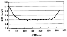
図19は、感光体走行距離がある程度まで大きくなった感光体における帯電電位Vdと、感光体の軸線方向における位置との関係を示すグラフである。A3サイズの画像幅=300mmに対して、作像幅を320mmとし、10mm位置と、160mm位置と、310mm位置とに反射型フォトセンサーを設けて帯電電位Vdを測定した結果に基づいて作成されたものである。感光体の軸線方向においては、端部箇所のほうが中央箇所に比べて帯電電位Vdが低下しており、地汚れを発生させ易くなることがわかる。 FIG. 19 is a graph showing the relationship between the charging potential Vd of the photosensitive member whose photosensitive member travel distance has increased to some extent and the position of the photosensitive member in the axial direction. A3 size image width = 300 mm, image width was set to 320 mm, and reflection photosensors were provided at 10 mm position, 160 mm position, and 310 mm position, and were created based on the result of measuring the charging potential Vd. Things. In the axial direction of the photoreceptor, the charging potential Vd is lower at the end portion than at the center portion, and it can be seen that background contamination is more likely to occur.
図20は、感光体走行距離がある程度まで大きくなった画像形成ユニットの帯電ローラの電気抵抗と、帯電ローラの軸線方向における位置との関係を示すグラフである。感光体走行距離がある程度大きくなると、帯電ローラの軸線方向の端部がシリカ(トナー添加剤)で汚れることで、端部の電気抵抗が中央部よりも上がる。これにより感光体の10mm位置と、160mm位置と、310mm位置とで帯電電位Vdの偏差が生ずる。 FIG. 20 is a graph showing the relationship between the electrical resistance of the charging roller of the image forming unit in which the photosensitive member travel distance has increased to some extent and the position of the charging roller in the axial direction. When the traveling distance of the photoconductor is increased to some extent, the end of the charging roller in the axial direction is stained with silica (toner additive), and the electric resistance of the end is higher than that of the center. As a result, a deviation of the charging potential Vd occurs at the 10 mm position, the 160 mm position, and the 310 mm position of the photoconductor.
そこで、本プリンタにおいては、Y,C,M,Kの各色の地汚れパターン及び位置特定用のトナー像の組み合わせを、感光体や帯電ローラの端部に対応するベルト幅方向端部に形成する。より詳しくは、各色についてそれぞれ、前述の組み合わせを、第1反射型フォトセンサー20aに対応するベルト幅方向一端部、又は第4反射型フォトセンサー20dに対応するベルト幅方向他端部に形成する。これにより、地汚れの発生を敏感に検知することができる。
Therefore, in the present printer, a combination of the background dirt pattern of each of the colors Y, C, M, and K and the toner image for specifying the position is formed at the belt width direction end corresponding to the end of the photoconductor or the charging roller. . More specifically, for each color, the above-described combination is formed at one end in the belt width direction corresponding to the first
なお、望ましくは、各色についてそれぞれ、前述の組み合わせをベルト幅方向一端部、ベルト幅方向他端部の両方に形成し、地汚れパターンの各区画のトナー付着量をそれぞれ一端部と他端部とで検知し、それらの平均値を求めることが望ましい。これにより、より適切な帯電バイアス補正量βを求めることができるようになる。 Preferably, for each color, the above-mentioned combination is formed at both the one end in the belt width direction and the other end in the belt width direction, and the toner adhesion amount of each section of the background dirt pattern is calculated as one end and the other end, respectively. It is desirable to detect them and obtain their average value. Thereby, a more appropriate charging bias correction amount β can be obtained.
図14に示されるように、本プリンタでは、地汚れパターンを形成する際に、帯電バイアスVcを段階的に上昇させている。これは、帯電バイアスを絶対値の大きな値から小さな値に段階的に変化させることを意味しており(帯電バイアスVcがマイナス極性であることから下降するほど絶対値が大きくなる)、地肌ポテンシャルを段階的に小さくしていくことになる。つまり、各区画を地汚れトナー量の小さなものから順に帯電バイアスVcの設定によって感光体に形成していく。地汚れが発生するということは、僅かではあるものの、現像剤のトナーが消費されてトナー濃度を低下させていることになる。地汚れトナー量の小さな区画から順に感光体に形成していくことで、地汚れパターンの先端から後端までを形成する過程でトナー濃度を少しずつ低下させていくようにしている。これにより、トナー濃度の低下に起因する区画に対する地汚れトナー量の不適切化を抑えて、地汚れ性能をより高精度に検出することができる。そして、トナーを多く消費する位置特定用のトナー像を地汚れパターンよりもベルト移動方向の後側に形成することで、その現像タイミングを地汚れパターン後端部の現像タイミングよりも後にしている。これにより、位置特定用のトナー像の現像によるトナー濃度の低下による地汚れ性能検出精度の低下を回避することができる。 As shown in FIG. 14, in the present printer, the charging bias Vc is increased stepwise when a background dirt pattern is formed. This means that the charging bias is changed stepwise from a large absolute value to a small absolute value (the absolute value increases as the charging bias Vc decreases since the charging bias Vc has a negative polarity), and the background potential is reduced. It will be gradually reduced. That is, each section is formed on the photoconductor by setting the charging bias Vc in ascending order of the amount of background toner. The occurrence of background contamination means that the toner of the developer is consumed, though slightly, and the toner concentration is reduced. The toner density is gradually reduced in the process of forming from the front end to the rear end of the background stain pattern by forming the photosensitive member in order from the section having the smallest background toner amount. As a result, it is possible to prevent the background soil toner amount from becoming inappropriate for the section caused by the decrease in the toner density and detect the background soil performance with higher accuracy. Then, by forming the toner image for specifying the position that consumes a large amount of toner on the rear side of the background dirt pattern in the belt moving direction, the development timing is set after the development timing of the rear end of the background dirt pattern. . As a result, it is possible to avoid a decrease in the detection accuracy of the background contamination performance due to a decrease in the toner density due to the development of the position specifying toner image.
また、位置特定用のトナー像については、必ずしも、地汚れパターンよりもベルト移動方向の前側や後側に形成する必要はない。例えば、図21に示されるように、位置特定用のYトナー像を、Y地汚れパターンYJPに対してベルト幅方向に並べて形成してもよい。図示の例では、第1反射型フォトセンサー20aによる検知位置を通るようにベルト幅方向の一端部に形成されたY地汚れパターンYJPの横に位置特定用のYトナー像YSTを形成している。そして、そのYトナー像YSTが第2反射型フォトセンサー20bによる検知位置に進入したタイミングに基づいて、一端部のY地汚れパターンYJPの各区画が第1反射型フォトセンサー20aによる検知位置に進入するタイミングを特定する。他端部のY地汚れパターンYJPの各区画が第4反射型フォトセンサー20dによる検知位置に進入するタイミングも特定する。かかる構成では、各区画の進入タイミングをより精度良く特定することができる。
Further, the toner image for position identification does not always need to be formed on the front side or the rear side in the belt moving direction of the background stain pattern. For example, as shown in FIG. 21, Y toner images for position identification may be formed in the belt width direction with respect to the Y background dirt pattern YJP. In the illustrated example, a Y toner image YST for position identification is formed beside the Y background dirt pattern YJP formed at one end in the belt width direction so as to pass through the detection position of the first
次に、実施形態に係るプリンタの特徴的な構成について説明する。
本発明者らは、実施形態に係るプリンタと同様の構成のプリンタ試験機を用いてプリントテストを行ったところ、上述した帯電バイアス調整制御を実施した直後に、画像濃度が大きく変化したり、細線の太さが大きく変化したりすることがあった。同時に、色味も大きく変化した。そこで、本発明者らは、面積階調法による16階調パターン像を形成してその色差△Eを測定する実験を行った。
Next, a characteristic configuration of the printer according to the embodiment will be described.
The present inventors performed a print test using a printer tester having the same configuration as the printer according to the embodiment, and immediately after performing the above-described charging bias adjustment control, the image density greatly changed, Sometimes changed greatly in thickness. At the same time, the color changed significantly. Therefore, the present inventors conducted an experiment in which a 16-gradation pattern image was formed by the area gradation method and the color difference ΔE was measured.
色差△Eについては、次のようにして測定した。即ち、プリンタ試験機によってC(シアン)、M(マゼンタ)の16階調パターン像を白色紙にプリントした。その後、帯電バイアスVcをそれまでの設定よりも50[V]だけ変化させてから、C、Mの16階調パターン像をもう一度プリントした。それらの16階調パターン像は、16階調目の階調部が矩形状外郭の内部の全てをトナーで覆った画像面積率100[%]のベタ画像部になっている。また、15階調目,14階調目,13階調目,12階調目,11階調目,10階調目の階調部の画像面積率が93.75[%],87.50[%],81.25[%],75.00[%],68.75[%],62.50[%]になっている。また、9階調目,8階調目,7階調目,6階調目,5階調目,4階調目の階調部の画像面積率が56.25[%],50.00[%],43.75[%],37.50[%],31.25[%],25.00[%]になっている。また、3階調目,2階調目,1階調目の階調部の画像面積率が18.75[%],12.50[%],6.25[%]になっている。15階調から1階調までは、階調数の減少につれて画像面積率を6.25[%]ずつ減じた画像面積率になっているのである。 The color difference ΔE was measured as follows. That is, 16 gradation pattern images of C (cyan) and M (magenta) were printed on white paper by a printer tester. Thereafter, the charging bias Vc was changed by 50 [V] from the previous setting, and then a 16-gradation pattern image of C and M was printed again. The 16-gradation pattern images are solid image portions having an image area ratio of 100 [%] in which the gradation portion of the 16th gradation covers the entire inside of the rectangular outline with toner. Further, the image area ratios of the gradation portions at the 15th gradation, the 14th gradation, the 13th gradation, the 12th gradation, the 11th gradation, and the 10th gradation are 93.75 [%] and 87.50. [%], 81.25 [%], 75.00 [%], 68.75 [%], and 62.50 [%]. Further, the image area ratios of the ninth gradation, the eighth gradation, the seventh gradation, the sixth gradation, the fifth gradation, and the fourth gradation are 56.25 [%] and 50.00. [%], 43.75 [%], 37.50 [%], 31.25 [%], and 25.00 [%]. In addition, the image area ratios of the third, second, and first gradation sections are 18.75 [%], 12.50 [%], and 6.25 [%]. From the 15th gradation to the 1st gradation, the image area ratio is reduced by 6.25 [%] as the number of gradations decreases.
測定器として、X−Rite社製のX−Rite938またはX−Rite939を用いて、帯電バイアスVcを変化させる前後の16階調パターン像間でのL*a*b*系での色差△Eを測定した。なお、測定器については、前述した二つの測定器と同等の性能のものであれば、他の測色器を用いてもよい。 Using X-Rite 938 or X-Rite 939 manufactured by X-Rite as a measuring device, the color difference ΔE in the L * a * b * system between the 16 gradation pattern images before and after changing the charging bias Vc was measured. It was measured. It should be noted that other color measuring devices may be used as long as they have the same performance as the two measuring devices described above.
図22は、この実験における色差△Eと16階調パターン像の階調数との関係を示すグラフである。図示のように、C、Mのそれぞれにおいて、1階調目、2階調目、3階調目、16階調目では、帯電バイアスVcを変化させる前後における色差△Eが比較的小さくなっている。色差△Eの比較的大きな階調に着目すると、Cでは、4階調目から10階調目までにおいて大きな変化が認められる。また、Mでは、9階調目から12階調目までにおいて大きな変化が認められる。それらの範囲では、帯電バイアスVcを変化させる前後で、画像濃度の大きな変化も認められた。また、それらの階調について、帯電バイアスVc変化前、変化後のそれぞれで細線画像を形成して、両者を比較したところ、太さの大きな変化も認められた。 FIG. 22 is a graph showing the relationship between the color difference ΔE and the number of gradations of the 16 gradation pattern image in this experiment. As illustrated, in each of C and M, the color difference ΔE before and after changing the charging bias Vc is relatively small at the first, second, third, and sixteenth gray levels. I have. Focusing on the relatively large gradation of the color difference ΔE, in C, a large change is recognized from the fourth gradation to the tenth gradation. In M, a large change is recognized from the ninth to the twelfth gradation. In these ranges, a large change in the image density was also observed before and after changing the charging bias Vc. Further, with respect to those gradations, a thin line image was formed before and after the change in the charging bias Vc, and the two were compared. As a result, a large change in thickness was recognized.
このような色差△Eの変化、細線の太さ変化、及び画像濃度変化が発生するのは、次のような理由によるものと考えられる。即ち、感光体に1ドットを書き込む光ビームは、図23(a)に示されるように、ビームスポットの半径方向の位置xにおけるスポット中心でエネルギーが最も強くなり、中心から外に向かうにつれてエネルギーが徐々に弱くなっていく。このような光ビームが、帯電電位Vd=V1[V]に帯電した感光体に照射されると、照射された部分は、光ビームエネルギー分布と感光体の感度特性との作用により、図23(b)に示されるような電位分布になる。電子写真プロセスでは、感光体表面のうち、電位の絶対値が現像バイアスVbの絶対値よりも小さくなっている部分にトナーが付着する。このため、1ドットに着目すると、図23(b)の例ではドット径がX1になる。一方、帯電電位VdをV2[V]まで上げたとする(|V1|<|V2|)。すると、図23(c)に示されるように、ビームスポットにおいて、現像バイアスVbよりも低電位になる領域がより小さくなる。この結果、ドット径がX1よりも小さいX2になる。 Such a change in the color difference ΔE, a change in the thickness of the thin line, and a change in the image density are considered to be due to the following reasons. That is, as shown in FIG. 23A, the energy of the light beam for writing one dot on the photoreceptor has the highest energy at the spot center at the radial position x of the beam spot, and the energy decreases outward from the center. It gradually weakens. When such a light beam is applied to the photoconductor charged to the charging potential Vd = V 1 [V], the irradiated portion is caused by the effect of the light beam energy distribution and the sensitivity characteristics of the photoconductor, as shown in FIG. The potential distribution is as shown in FIG. In the electrophotographic process, toner adheres to a portion of the photoconductor surface where the absolute value of the potential is smaller than the absolute value of the developing bias Vb. Therefore, paying attention to one dot, the dot diameter becomes X 1 in the example of FIG. 23 (b). On the other hand, it is assumed that the charging potential Vd is raised to V 2 [V] (| V 1 | <| V 2 |). Then, as shown in FIG. 23C, the area of the beam spot where the potential is lower than the developing bias Vb becomes smaller. As a result, the dot diameter becomes X2 smaller than X1.
帯電バイアス調整処理において、帯電バイアスVcの調整量を大きくし過ぎると、それに伴って帯電電位Vdを大きく変化させることから、調整前後でドット径を大きく変化させる。これにより、画像の面積階調部では、ドット数が同じであっても、ドットの占める面積率が異なってくることから、画像濃度が変動してしまう。また、細線では、調整前後で太さが大きく変化してしまう。また、互いに異なる一次色(Y,C,M,K)を二つ重ね合わせた二次色の画像部や、一次色を三つ重ね合わせた三次色の画像部では、調整前後で一次色の色差△Eが大きく変化することで、色味が大きく変化してしまう。 In the charging bias adjustment processing, if the adjustment amount of the charging bias Vc is excessively increased, the charging potential Vd is greatly changed accordingly, so that the dot diameter is largely changed before and after the adjustment. As a result, in the area gradation part of the image, even if the number of dots is the same, the area ratio occupied by the dots differs, so that the image density fluctuates. In the case of a thin line, the thickness greatly changes before and after the adjustment. In a secondary color image portion in which two different primary colors (Y, C, M, K) are superimposed, or in a tertiary color image portion in which three primary colors are superimposed, the primary color before and after the adjustment is used. When the color difference ΔE changes significantly, the tint greatly changes.
このような不具合を抑えるためには、帯電電位Vdの増減に伴って現像バイアスVbも増減させればよいのであるが、そうすると、地肌ポテンシャルを変化させることができずに、地汚れやキャリア付着を引き起こしてしまう。このため、帯電電位Vdの増減に伴って現像バイアスVbを増減させることはできない。 In order to suppress such a problem, the developing bias Vb may be increased or decreased in accordance with the increase or decrease in the charging potential Vd. However, in this case, the background potential cannot be changed, and background contamination and carrier adhesion may be reduced. Cause it. For this reason, the developing bias Vb cannot be increased or decreased with the increase or decrease of the charging potential Vd.
本発明者らは、プリンタ試験機を用いて、第二プリントテストを実施した。この第二プリントテストでは、Mの一色について、帯電バイアスVcを変化させる前後において、16階調における10階調目のハーフトーンパッチトナー像を形成して両者の色差△Eを測定した。色差△Eを最も大きくした10階調目に着目したのである。帯電バイアスVcの変化後については、変化直後の初期、及び変化後に所定枚数のハーフトーンパッチトナー像を出力した時点の経時、の二つのタイミングでそれぞれ色を測定し、それぞれについて調整前との色差△Eを算出した。帯電バイアスVcの変化量については、−50[V]、−30[V]、0[V]、30[V]、50[V]の5通りを採用した。 The present inventors performed a second print test using a printer tester. In the second print test, for one color of M, before and after changing the charging bias Vc, a halftone patch toner image of the tenth gradation in 16 gradations was formed, and the color difference ΔE between the two was measured. Attention was paid to the tenth gradation in which the color difference ΔE was maximized. After the change in the charging bias Vc, the color is measured at two timings, the initial stage immediately after the change, and the lapse of time when a predetermined number of halftone patch toner images are output after the change, and the color difference between each is measured. ΔE was calculated. Regarding the amount of change in the charging bias Vc, five types of -50 [V], -30 [V], 0 [V], 30 [V], and 50 [V] were adopted.
この第二テストプリントにおける色差△Eと帯電バイアス変更量との関係を図24に示す。図示のように、第二テストプリントにおける色差△Eの最大値は10より少し大きな値であり、この最大値は、帯電バイアス変更量=50[V]の変更をしてから連続プリント後(経時)に発生したものである。本発明者らは、別の実験により、色差△Eを10以下に留めれば、帯電バイアス調整制御を実施することによる色味変化量、細線太さ変化量、画像濃度変化量をそれぞれぎりぎり許容範囲内に留め得ることを見出した。同図より、その条件を満足させるためには、帯電バイアス調整制御における帯電バイアス変更量の上限値(以下、上限調整量という)を30[V]にすればよいことがわかる。 FIG. 24 shows the relationship between the color difference ΔE and the charging bias change amount in the second test print. As shown in the figure, the maximum value of the color difference ΔE in the second test print is a value slightly larger than 10, and this maximum value is changed after the change of the charging bias change amount = 50 [V] and after the continuous printing (time ). According to another experiment, if the color difference ΔE is kept at 10 or less, the color change amount, the fine line thickness change amount, and the image density change amount due to the execution of the charging bias adjustment control are each allowed. It has been found that it can be kept within the range. From the figure, it can be seen that in order to satisfy the condition, the upper limit (hereinafter referred to as the upper limit adjustment amount) of the charging bias change amount in the charging bias adjustment control should be set to 30 [V].
このようにして求めた上限調整量を限度として帯電バイアス調整制御で帯電バイアスVcを調整するように制御部30を構成すれば、色味変化量、細線太さ変化量、及び画像濃度変化量を何れも許容範囲内に収めることができる。具体的には、16階調パターン像のテストプリントを実施して帯電バイアス変更後の初期及び経時のそれぞれについて、変更前との色差△Eを測定し、4階調から12階調までの色差△のそれぞれを許容限界以下にする上限調整量を求める。そして、その範囲内で帯電バイアスVcを調整させるように制御部30を構成するのである。もちろん、16階調すべてについて色差ΔEを測定し、全てを許容範囲内に収めるようにしてもよい。なお、C,Mの二色だけの実験結果を示したが、Yも同様の実験結果になった。また、Kも、細線の太さや画像濃度については、Y,C,Mと同様の実験結果になった。
If the
そこで、実施形態に係るプリンタにおいては、帯電バイアス調整制御において、上限調整量=30[V](これは絶対値でありプラス側、マイナス側のいずれも30V)の範囲内で帯電バイアスVcを補正するように、制御部30を構成している。
Therefore, in the printer according to the embodiment, in the charging bias adjustment control, the charging bias Vc is corrected within the range of the upper limit adjustment amount = 30 [V] (this is an absolute value and both the plus side and the minus side are 30 V). The
次に、実施形態に係るプリンタに、より特徴的な構成を付加した各実施例のプリンタについて説明する。なお、以下に特筆しない限り、各実施例に係るプリンタの構成は、実施形態と同様である。
[第一実施例]
実施形態に係るプリンタでは、帯電バイアスVcの上限調整量を、色差ΔEを10以下に留め得る30[V]に設定した。しかしながら、近年のプロダクションプリンティングマシンにおいては、従来のオフセット印刷機との代替を図るために、色差ΔEを5以下、好ましくは3以下にすることが望まれるようになってきている。そのようなニーズに対応すべく、第一実施例に係るプリンタに特徴的な構成を設けている。以下、この特徴的な構成について説明する。
Next, a description will be given of a printer according to each embodiment in which a more characteristic configuration is added to the printer according to the embodiment. Unless otherwise noted below, the configuration of the printer according to each embodiment is the same as that of the embodiment.
[First embodiment]
In the printer according to the embodiment, the upper limit adjustment amount of the charging bias Vc is set to 30 [V] at which the color difference ΔE can be kept to 10 or less. However, in recent production printing machines, it has been desired that the color difference ΔE be 5 or less, preferably 3 or less in order to replace the conventional offset printing press. In order to meet such needs, the printer according to the first embodiment is provided with a characteristic configuration. Hereinafter, this characteristic configuration will be described.
第一実施例に係るプリンタでは、階調再現時に用いる変換テーブルを必要に応じて補正するようになっている。この補正については、帯電バイアス調整制御を実施した直後に、必要に応じて実施する。実施する場合には、まず、所定の面積階調パターン像を形成して、その面積階調パターン像における各階調部の画像濃度(トナー付着量)を検知する。そして、各階調部について狙いの画像濃度からのずれ量を把握した結果に基づいて、各階調部で狙いの画像濃度が得られるように、階調再現条件たる変換テーブルを補正する。この変換テーブルは、各一次色の各画素の階調値(一次色毎の画素値)を入力データとし、その入力データを狙いの画像濃度が得られる階調値に変換して出力データとするためのものである。この変換テーブルに基づいて、画像データの各画素の階調値を変換し、変換後の階調値に基づいて画像を形成することで、狙いの画像濃度を得ることができる。各画素の各一次色の階調値のそれぞれは、0から255までの256階調で表現されている。 In the printer according to the first embodiment, the conversion table used for tone reproduction is corrected as necessary. This correction is performed as needed immediately after the charging bias adjustment control is performed. When performing the process, first, a predetermined area gradation pattern image is formed, and the image density (toner adhesion amount) of each gradation portion in the area gradation pattern image is detected. Then, based on the result of grasping the deviation amount from the target image density for each gradation part, the conversion table as the gradation reproduction condition is corrected so that the target image density can be obtained in each gradation part. In this conversion table, the gradation value (pixel value for each primary color) of each pixel of each primary color is used as input data, and the input data is converted into a gradation value at which a target image density can be obtained and output data is obtained. It is for. The target image density can be obtained by converting the tone value of each pixel of the image data based on the conversion table and forming an image based on the converted tone value. Each gradation value of each primary color of each pixel is represented by 256 gradations from 0 to 255.
一般に、作像性能が経時変化すると、0から255までのデータ上の階調変化に対し、実際の画像濃度はリニアに変化せずに、例えば図25の帯電バイアス調整前のように、曲線状のグラフ特性になってくる。そこで、図25における帯電バイアス調整前のような曲線状のグラフを、直線状のグラフに変化させるように、変換テーブルを補正するのである。この補正を、図示のように、帯電バイアス調整制御の直後に実施することで、色差△Eを、10以下よりも優れた5以下や3以下にすることが可能になる。 In general, when the image forming performance changes with time, the actual image density does not change linearly with respect to the gradation change on the data from 0 to 255, and for example, as shown in FIG. Graph characteristics. Therefore, the conversion table is corrected so that the curved graph before charging bias adjustment in FIG. 25 is changed to a linear graph. By performing this correction immediately after the charging bias adjustment control as shown in the figure, it is possible to reduce the color difference ΔE to 5 or less, which is better than 10 or less.
図26は、第一実施例に係るプリンタの制御部30によって実施される制御フローを示すフローチャートである。この制御フローは、帯電バイアス調整制御の開始条件(トリガー)を満足したことに基づいて開始される。制御部30は、帯電バイアス調整制御を実施した後(S1)、直前の帯電バイアス調整処理における帯電バイアスVcの調整量について所定の閾値を超えているか否かを判定する(S2)。この閾値は、予めの実験結果に基づいて設定されているもので、色差△Eを高品質用狙いの5以下、あるいは3以下に留め得る値になっている。このため、直前の帯電バイアス調整制御における調整量が閾値を超えている場合には、色差△Eを高品質用狙い以下にすることができない状態になっている。そこで、調整量が閾値を超えている場合(S2でY)には、変換テーブルを補正するために、後述するS3からS6のフローを実施する。これに対し、調整量が閾値を超えていない場合(S2でN)には、一連の処理フローを終える。
FIG. 26 is a flowchart illustrating a control flow performed by the
変換テーブルを補正する場合には、まず、16階調の面積階調パターン像を形成し(S3)、そのパターンにおける各階調部のそれぞれの画像濃度(トナー付着量)を光学センサーユニット20で検知する(S4)。そして、図26における帯電バイアス調整後のグラフのように、各画像濃度値と各階調値との関係について線形特性になる直線近似式を求めた後(S5)、この直線近似式に基づいて、変換テーブルを補正する(S6)。以上の処理を、Y,C,M,Kの各色のそれぞれで個別に実施する。このような変換テーブルの補正により、例えば図26に示されるように、ある画像濃度値について、帯電バイアス調整前に階調値X1で処理していたものを、階調値X2で処理するようになる。これにより、色差△Eを高品質用狙い(例えば3や5)以下にすることが可能になる。
When correcting the conversion table, first, an area gradation pattern image of 16 gradations is formed (S3), and the image density (toner adhesion amount) of each gradation portion in the pattern is detected by the
図27は、変換テーブルの補正の有無と、テストプリントにおける色差△Eの最大値と、帯電バイアス調整制御における上限調整量との関係を示すグラフである。図示のように、変換テーブルの補正を実施しない場合には、色差△Eの最大値が帯電バイアスVcの上限補正量に対応した値(標準の狙い)になる。これに対し、変換テーブルの補正を実施する場合には、色差△Eの最大値を高品質用の狙いにすることが可能になる。 FIG. 27 is a graph showing the relationship between the presence or absence of correction in the conversion table, the maximum value of the color difference ΔE in the test print, and the upper limit adjustment amount in the charging bias adjustment control. As shown, when the correction of the conversion table is not performed, the maximum value of the color difference ΔE becomes a value (standard aim) corresponding to the upper limit correction amount of the charging bias Vc. On the other hand, when the conversion table is corrected, the maximum value of the color difference ΔE can be aimed at for high quality.
第一実施例では、変換テーブルを補正するために形成する面積階調パターン像として16階調のものを採用したが、階調数はこれに限られるものではない。16階調よりも増やしてもよいし、上述したように色差△Eが特に大きくなる4階調目から12階調目の階調部だけを形成してもよい。また、Y,C,M,Kのうち、何れか一色でも帯電バイアスVcの調整量が閾値を超えた場合には、全ての色について変換テーブルを補正するようにしてもよい。 In the first embodiment, the area gradation pattern image formed to correct the conversion table has 16 gradations, but the number of gradations is not limited to this. The number of gradations may be increased from the 16th gradation, or only the 4th to 12th gradation parts where the color difference ΔE is particularly large as described above may be formed. When the adjustment amount of the charging bias Vc exceeds the threshold value for any one of the colors Y, C, M, and K, the conversion table may be corrected for all the colors.
なお、変換テーフルの補正によって細線の太さの変化を抑えることはできないが、これについては、階調値の変更量に応じてライン幅を補正するライン幅補正処理を実施ことで対応できる。例えば、図26に示されるように階調値をX1からX2に変更した場合に、その差である「X2−X1」に応じてライン幅を変更する処理である。ライン幅の変更については、オリジナルの画像データにおいて1ドット幅のラインを出力すべきところを、「X2−X1」の値に応じたドット数の幅のラインに変更すればよい。このようにすれば、細線の太さの変化量についても、高品質用狙い以下に留めることが可能になる。階調値の変更量に対してどの程度のドット数で幅を変えるかについては、機種仕様によって異なってくる。よって、帯電バイアスVcの調整量と、階調値の変更量と、ライン幅の変化量とを実験によって測定した結果に基づいて、階調値の変更量からライン幅の変更量を求めるためのアルゴリズムを構築する。 Note that the change in the thickness of the thin line cannot be suppressed by correcting the conversion table, but this can be dealt with by performing a line width correction process for correcting the line width according to the amount of change in the gradation value. For example, as shown in FIG. 26, when the gradation value is changed from X1 to X2, the line width is changed according to the difference “X2−X1”. Regarding the change of the line width, it is sufficient to change the line to output a line of 1 dot width in the original image data to a line of the number of dots corresponding to the value of “X2−X1”. By doing so, it is possible to keep the amount of change in the thickness of the thin line below the target for high quality. The number of dots to change the width with respect to the change amount of the gradation value depends on the model specifications. Therefore, based on the result of experimentally measuring the adjustment amount of the charging bias Vc, the change amount of the gradation value, and the change amount of the line width, it is necessary to obtain the change amount of the line width from the change amount of the gradation value. Build the algorithm.
[第二実施例]
帯電バイアス調整制御では、帯電バイアスVcを段階的に変化させながら地汚れパターンを形成する都合上、ユーザーの命令に基づく画像を形成することができない。このため、実施に伴って装置のダウンタイムを増加させてしまう。実施形態に係るプリンタでは、感光体走行距離が10[km]以上になり、且つ温度が10[℃]以下になるか、あるいは絶対湿度が適正でなくなるかした場合には、必ず帯電バイアス調整制御が実施されることになる。しかしながら、温度が例えば6[℃]などと比較的低かったり、絶対湿度が適正でなかったり(低すぎたり高すぎたり)しても、前回においてその温度や湿度の条件、あるいはそれに近い条件で帯電バイアス調整制御を実施していれば、今回の実施の必要性は低い。
[Second embodiment]
In the charging bias adjustment control, it is not possible to form an image based on a user's command because the background bias pattern is formed while changing the charging bias Vc stepwise. For this reason, the downtime of the apparatus increases with the implementation. In the printer according to the embodiment, when the travel distance of the photosensitive member is equal to or more than 10 [km] and the temperature is equal to or less than 10 [° C.] or the absolute humidity is not appropriate, the charging bias adjustment control is always performed. Will be implemented. However, even if the temperature is relatively low, for example, 6 [° C.], or the absolute humidity is not appropriate (too low or too high), charging is performed in the previous condition under the temperature or humidity condition or a condition close thereto. If the bias adjustment control has been performed, the necessity of this implementation is low.
そこで、第二実施例に係るプリンタの制御部30は、帯電バイアス調整制御を実施したときに環境センサー52による環境の検知結果をRAMに記憶しておく。そして、帯電バイアス調整制御の実施の必要性を判定するときに、温度が比較的低かったり、絶対湿度が適正でなかったりした場合であっても、次のような場合には、帯電バイアス調整制御を実施しないことにする。即ち、前回の帯電バイアス調整制御実施時からの温度変化量が比較的小さかったり、絶対湿度変化量が比較的小さかったりした場合である。このようにすることで、帯電バイアス調整制御を不要に実施することによる装置のダウンタイムの発生を回避することができる。
Therefore, the
帯電バイアス調整制御では、パッチ状トナー像を検知するプロセスコントロール処理とは異なり、地肌部というトナー付着量の極めて少ない感光体領域のトナー付着量を検知する。このため、例えばトナー飛散によるトナー付着など、地肌ポテンシャルとは直接的に関連しない突発的な要因によって地肌部に付着したトナーを敏感に検知したことにより、帯電バイアスVcを不要に大きな調整量で調整してキャリア付着を引き起こすことがある。 In the charging bias adjustment control, unlike the process control processing for detecting a patch-like toner image, the toner adhesion amount in a photoconductor region having a very small toner adhesion amount, such as a background portion, is detected. For this reason, the charging bias Vc is adjusted with an unnecessarily large adjustment amount by sensitively detecting toner adhering to the background portion due to a sudden factor that is not directly related to the background potential such as toner adhesion due to toner scattering. Carrier adhesion.
そこで、制御部30は、帯電バイアス調整処理を実施したときに、そのときの帯電バイアスVcの調整量をRAMに記憶しておく。そして、次回のプロセスコントロール処理を実施した後に、帯電バイアス調整制御の必要性を判定する際に、前回の帯電バイアス調整制御における調整量が比較的大きい場合には、環境によらず帯電バイアス調整制御を実施するようになっている。
Therefore, when the charging bias adjustment process is performed, the
図28は、第二実施例に係るプリンタの制御部30によって実施される定期ルーチン処理の流れを示すフローチャートである。このフローチャートにおける主な流れは、図13の定期ルーチン処理と同様であるので、図13の定期ルーチン処理と異なる点だけを説明する。図28において、S1〜S3までの流れは図13のフローチャートと同じである。制御部30は、前回の帯電バイアス調整制御を実施してからの感光体走行距離が10[km]以上になったか否かを判定するS4の工程を実施する前に、調整量についての判定を行う。具体的には、前回の帯電バイアス調整制御における帯電バイアスVcの調整量について15[V]を超えているか否かを判定する(S11)。一般に、帯電電位Vdが狙いからずれていく現象は徐々に起こるため、帯電バイアス調整制御で帯電バイアスVcが大きく調整されることは少ない。このため、大きく調整された場合には、感光体地肌部に対して突発的な要因によって付着したトナーが検知されたことにより、調整量が不要に大きくなってしまっている可能性がある(以下、このケースを「不要調整」という)。そこで、制御部30は、調整量が15[V]を超えている場合には(S11でN)、環境にかかわらず帯電バイアス調整制御を実施するために、処理フローをS7に進める。これにより、前回の帯電バイアス調整制御で「不要調整」が発生して帯電電位Vdが不要に高くなっている場合に、帯電電位Vdを迅速に適切な値まで下げて、感光体の不要な劣化を抑えることができる。
FIG. 28 is a flowchart illustrating a flow of a periodic routine process performed by the
なお、第二実施例では、大きく調整されたか否かの判断基準として、15[V]を採用しているが、その理由は、予めの実験によって15[V]の場合に「不要調整」の発生率が10[%]になることが判明したからである。発生率がより高くなる値や、より低くなる値を基準にしてもよい。 In the second embodiment, 15 [V] is adopted as a criterion for judging whether or not the adjustment has been made large. This is because the occurrence rate was found to be 10%. A value with a higher incidence or a value with a lower incidence may be used as a reference.
制御部30は、S5の工程で10[℃]以下であると判定した場合には(S5でY)、そのままフラグをセットしないで、前回の帯電バイアス調整制御を実施してから現時点に至るまでの温度変化量について比較的大きいか否かを判定する(S12)。例えば、温度変化量が2[℃]以上である場合に比較的大きいと判定する。そして、比較的大きい場合には(S12でY)、フラグをセットした後に帯電バイアス調整制御を実施する(S7→S9→S10)。一方、温度変化量が比較的大きくない場合には(S12でN)、帯電バイス調整制御を実施せず、それまでと同じ値の帯電バイアスVcを採用することにして、帯電バイアスVcを調整しないままにする(S14)。これにより、帯電バイアス調整制御を不要に実施することによるダウンタイムの増加を回避することができる。
If the
また、制御部30は、絶対湿度について適正でないと判定した場合には(S6でN)、そのままフラグをセットしないで、前回の帯電バイアス調整制御を実施してから現時点に至るまでの絶対湿度変化量について比較的大きいか否かを判定する(S13)。例えば、絶対湿度変化量が2[mg/m3]以上である場合に比較的大きいと判定する。そして、比較的大きい場合には(S13でY)、フラグをセットした後に帯電バイアス調整制御を実施する(S7→S9→S10)。一方、絶対湿度変化量が比較的大きくない場合には(S13でN)、帯電バイス調整制御を実施せず、それまでと同じ値の帯電バイアスVcを採用することにして、帯電バイアスVcを調整しないままにする(S14)。これにより、帯電バイアス調整制御を不要に実施することによるダウンタイムの増加を回避することができる。
When the
[第三実施例]
第二実施例では、前回の帯電バイアス調整制御実施時からの環境変化量が大きくない場合には帯電バイアス調整制御を実施しないようにしたが、逆に環境が急変しているような場合には、帯電バイアス調整制御を頻繁に実施することが望ましいケースがある。稀ではあるが、寒冷地の朝など、マシンが冷え切った状帯でメインスイッチが入れられ、プロセスコントロールなどが完了した後、暖房が効きだすようなケースである。このようなケースでは、マシンの起動とともに急速に帯電装置や感光体の温度が上昇することから、帯電バイアス調整制御を細かい時間間隔で定期的に実施することが望ましい。
[Third embodiment]
In the second embodiment, the charging bias adjustment control is not performed when the environment change amount from the previous charging bias adjustment control execution is not large, but when the environment is suddenly changed, In some cases, it is desirable to frequently perform charging bias adjustment control. In rare cases, such as in the morning of a cold region, when the main switch is turned on when the machine is completely cold and process control is completed, heating will be effective. In such a case, since the temperatures of the charging device and the photoreceptor rapidly rise with the start of the machine, it is desirable to periodically perform the charging bias adjustment control at small time intervals.
そこで、第三実施例に係るプリンタの制御部30は、環境センサー52による温度の検知結果や、絶対湿度の算出結果を、所定時間経過後毎、所定枚数プリント毎などの定期的なタイミングでRAMに記憶する。そして、前回記憶時からの温度変化量や絶対湿度変化量が所定値以上である場合には、帯電バイアス調整制御を実施する。このとき、プリントジョブ中である場合には、プリントジョブ終了後に帯電バイアス調整制御を実施する。これにより、環境が急変している場合に、適切なタイミングで帯電バイアス調整制御を実施して環境の急変に起因する地汚れやキャリア付着の発生を抑えることができる。
Therefore, the
[第四実施例]
上述したように、通常の電子写真式の画像形成装置では、色差△Eを10以下にする値に帯電バイアスVcの上限調整量を設定すれば、帯電バイアスVcを調整することによる色味変化量、細線の太さ変化量、画像濃度変化量を許容範囲に留めることができる。しかし、プロダクションプリンティングの分野では、さらに厳しい要求が出てきている。かかる要求に対しては、色差△Eを経時的に大きくしていかないように、帯電バイアス調整制御を実施することが望ましい。
[Fourth embodiment]
As described above, in a normal electrophotographic image forming apparatus, if the upper limit adjustment amount of the charging bias Vc is set to a value that makes the
そこで、第四実施例に係るプリンタでは、図3に示されるように、制御部30にデータを入力するための入力装置53を接続している。そして、情報入力手段たる入力装置53により、上限調整量を補正するための補正情報として、係数情報を入力するようになっている。制御部30は、ユーザーによって係数情報が入力されると、それをRAMに記憶する。そして、帯電バイアス調整制御において、RAMに記憶している上限調整量をそのまま採用するのではなく、前述した係数情報の係数の乗算によって補正した上限調整量を採用する。
Therefore, in the printer according to the fourth embodiment, as shown in FIG. 3, an
かかる構成では、帯電バイアスVcを調整することによる色味変化量、細線の太さ変化量、画像濃度変化量の上限を、ユーザーの好みに合わせて変更することができる。なお、ここでいう入力装置53は、一般的な複写機やプリンタにある操作パネルであってもよいし、パソコンなどからのデータを受けるものであってもよい。
In such a configuration, the amount of change in tint, the amount of change in the thickness of a thin line, and the upper limit of the amount of change in image density by adjusting the charging bias Vc can be changed according to the user's preference. Here, the
[第五実施例]
第五実施例に係るプリンタは、他の同じ構成のプリンタとともに、管理装置に通紙可能に接続されている。それらプリンタと管理装置との組み合わせにより、画像形成システムが構成されている。近年、故障予測や課金管理を行うために、複数の画像形成装置を回線によって通信可能な状態にし、管理装置に情報を集めて故障予測や課金情報を管理するシステムが実用化されている。複数の画像形成装置の稼働情報を所定のタイミングでインターネット回線などを通じて管理装置に送り、管理装置でマシン稼働情報を解析して故障予測を行ったり、課金を行ったりするものである。前述の画像形成システムも、そのような用途で、第五実施例に係る複数のプリンタと、管理装置とを通信可能にしている。
[Fifth embodiment]
The printer according to the fifth embodiment is connected to the management device so as to be able to pass paper, together with other printers having the same configuration. An image forming system is configured by a combination of the printer and the management device. In recent years, in order to perform failure prediction and charging management, a system that puts a plurality of image forming apparatuses into a communicable state via a line, collects information in a management device, and manages failure prediction and charging information has been put to practical use. The operation information of a plurality of image forming apparatuses is sent to a management apparatus via an Internet line or the like at a predetermined timing, and the management apparatus analyzes the machine operation information to perform a failure prediction or charge. The above-described image forming system also enables the plurality of printers according to the fifth embodiment to communicate with the management device for such purposes.
この画像形成システムは、図29に示されるように、複数の第五実施例に係るプリンタ1800が回線によって管理装置200とつながっている。管理装置200は、それらプリンタ100のうち、一括納品などにより、ほぼ同じ環境下に置かれるであろうと推測されるもの同士を、同一群に属するものとして紐付けしたデータベースを記憶している。プリンタ100は、感光体走行距離や環境などに基づいて帯電バイアス調整制御の実施について必要であると判定した場合、環境センサー52による検知結果を管理装置200に送信する。管理装置200は、何れかのプリンタ100から環境の検知結果が送信されてくると、検索処理を行う。具体的には、そのプリンタ100と同一の群に属するものとして紐付けされた他のプリンタ100のうち、過去に前述の検知結果に近い環境下で帯電バイアス調整制御を実施したものがないか否かを、既に記憶している過去実績データの中から検索する。そして、該当するプリンタ100が存在した場合には、そのプリンタ100が前記環境下で帯電バイアス調整制御を実施した後に送信してきた帯電バイアスVcの調整量を過去実績データから読み込む。更に、前述の検知結果を送信してきたプリンタ100に読み込み結果を送信する。これに対し、該当するプリンタ100が存在しない場合には、前述の検知結果を送信してきたプリンタ100に帯電バイアス調整制御の実施命令信号を送信する。
In this image forming system, as shown in FIG. 29, a plurality of printers 1800 according to the fifth embodiment are connected to the
環境センサー52による検知結果を管理装置200に送信したプリンタ100は、その後、帯電バイアスVcの調整量の情報が管理装置200から送信されてきた場合には、次のような処理を行う。即ち、帯電バイアス調整制御を実施する代わりに、その調整量と同じ分だけ帯電バイアスVcを調整する。これに対し、実施命令信号が管理装置200から送信されてきた場合には、帯電バイアス調整制御を実施する。
The
かかる構成において、同一群に属する複数のプリンタ100のうち、ある環境のもとで何れか一つのプリンタ100が帯電バイアス調整制御を行ったとする。この場合、同様の環境で他のプリンタに対して帯電バイアス調整制御を実施させることなく帯電バイアスVcを適切に調整させて、そのプリンタのダウンタイムの発生を抑えることができる。
In such a configuration, it is assumed that one of the plurality of
以上に説明したものは一例であり、本発明は、次の態様毎に特有の効果を奏する。
[態様A]
態様Aは、潜像担持体(例えば感光体2)と、前記潜像担持体の表面を帯電させる帯電手段(例えば帯電ローラ3)と、前記帯電手段に供給する帯電バイアスを出力する帯電電源(例えば帯電電源ユニット50)と、帯電後の前記表面に静電潜像を書き込む潜像書込手段(例えば光書込ユニット6)と、前記静電潜像を現像してトナー像を得る現像手段(例えば現像装置4)と、トナー像を前記表面から転写体に転写する転写手段(例えば一次転写ローラ9や一次転写電源)と、前記潜像担持体又は前記転写体の表面におけるトナー付着量を検知するトナー付着量検知手段(例えば光学センサーユニット20)と、地肌ポテンシャルを段階的に変化させながら前記潜像担持体の表面に地汚れパターンを形成し、前記地汚れパターンのトナー付着量を前記トナー付着量検知手段によって検知した結果に基づいて、前記帯電電源からの帯電バイアスの出力値を所定の上限調整量の範囲内で調整する帯電バイアス調整制御を実施する制御手段(例えば制御部30)とを備える画像形成装置であって、前記上限調整量が、面積階調によってベタ部よりも画像濃度を低減された面積階調部の色差△Eを所定値以下にする値に設定されていることを特徴とするものである。
What has been described above is merely an example, and the present invention has specific effects for each of the following aspects.
[Aspect A]
Aspect A includes a latent image carrier (for example, photoconductor 2), a charging unit (for example, charging roller 3) for charging the surface of the latent image carrier, and a charging power source (for outputting a charging bias supplied to the charging unit). For example, a charging power supply unit 50), a latent image writing unit (for example, an optical writing unit 6) for writing an electrostatic latent image on the charged surface, and a developing unit for developing the electrostatic latent image to obtain a toner image (For example, the developing device 4), a transfer unit (for example, a
かかる構成では、上限調整量を色差△Eが所定値以下となる値に設定しているので、帯電バイアス調整処理による調整前後における細線の太さの変化、中間調部の画像濃度の変化、及び色味の変化を何れも目立たないレベルまで低減することができる。 In such a configuration, since the upper limit adjustment amount is set to a value at which the color difference ΔE is equal to or less than a predetermined value, a change in the thickness of the thin line before and after the adjustment by the charging bias adjustment process, a change in the image density of the halftone portion, and Any change in color can be reduced to an inconspicuous level.
[態様B]
態様Bは、態様Aであって、前記潜像担持体が感光体であり、前記潜像書込手段が光照射によって潜像を書き込む露光装置(例えば光書込ユニット)であり、前記トナー付着量検知手段が前記潜像担持体又は前記転写体の光反射率を検知する反射型光学センサー(例えば光学センサーユニット20)であることを特徴とするものである。
[Aspect B]
Aspect B is an aspect A, wherein the latent image carrier is a photosensitive member, the latent image writing means is an exposure device (for example, an optical writing unit) for writing a latent image by light irradiation, and the toner adhesion The amount detecting means is a reflection type optical sensor (for example, an optical sensor unit 20) for detecting the light reflectance of the latent image carrier or the transfer body.
[態様C]
態様Cは、態様A又はBであって、前記所定値が10であることを特徴とするものである。かかる構成においては、帯電バイアス調整制御の実施前後のドット小径化を一般的な画像形成装置の性能レベルにする。これにより、帯電バイアス調整処理による調整前後における細線の太さの変化、中間調部の画像濃度の変化、及び色味の変化を一般的なユーザーが許容できるレベルに抑えることができる。
[Aspect C]
Aspect C is aspect A or B, wherein the predetermined value is 10. In such a configuration, the dot diameter reduction before and after the execution of the charging bias adjustment control is set to the performance level of a general image forming apparatus. As a result, a change in the thickness of the thin line, a change in the image density of the halftone portion, and a change in the color before and after the adjustment by the charging bias adjustment process can be suppressed to a level that can be accepted by a general user.
[態様D]
態様Dは、態様A〜Cの何れかであって、前記面積階調部が、16階調目を画像面積率100[%]の階調とし、15階調目から1階調目までのそれぞれを階調数の減少につれて画像面積率を6.25[%]ずつ減じた階調とする16階調のうち、4階調から12階調までの各面積階調部であることを特徴とするものである。かかる構成においては、帯電バイアスの変化に伴って色差△を変化させ易い4階調から12階調の面積階調部で色差△Eを所定値以下にすることで、次のような効果を奏することができる。即ち、帯電バイアス調整前後における細線の太さの変化、中間調部の画像濃度の変化、及び色味の変化を確実に抑えることができる。
[Aspect D]
Aspect D is any one of Aspects A to C, wherein the area gradation unit sets the 16th gradation as the gradation of the image area ratio 100 [%] and sets the 16th gradation as the gradation from the 15th gradation to the 1st gradation. Each of the 16 gray scales, in which the image area ratio is reduced by 6.25 [%] as the number of gray scales decreases, is an area gray scale portion from 4 gray scales to 12 gray scales. It is assumed that. In such a configuration, the following effects can be obtained by setting the color difference ΔE to be equal to or less than a predetermined value in the area gradation portion of 4 to 12 gradations in which the color difference Δ is easily changed with the change of the charging bias. be able to. That is, a change in the thickness of a thin line, a change in image density in a halftone portion, and a change in color before and after the charging bias adjustment can be reliably suppressed.
[態様E]
態様Eは、態様A〜D4の何れかにおいて、所定の面積階調パターン像を形成し、この面積階調パターン像の各階調部のトナー付着量を前記トナー付着量検知手段によって検知した結果に基づいて、面積階調再現条件(例えば変換テーブル)を補正するように、前記制御手段を構成したことを特徴とするものである。かかる構成では、第一実施例で説明したように、変換テーブルを補正することで、色差△Eを高品質用の狙いまで低減することができる。
[Aspect E]
In the mode E, the predetermined area gradation pattern image is formed in any one of the modes A to D4, and the toner adhesion amount of each gradation portion of the area gradation pattern image is detected by the toner adhesion amount detecting means. The control means is configured to correct an area gradation reproduction condition (for example, a conversion table) based on the control information. In such a configuration, as described in the first embodiment, by correcting the conversion table, the color difference ΔE can be reduced to the target for high quality.
[態様F]
態様Fは、態様A〜Eの何れかにおいて、環境を検知する環境検知手段(例えば環境センサー52)を設け、前記帯電バイアス調整制御を実施するか否かを決定する際に、前回の帯電バイアス調整制御における帯電バイアスの調整量が所定の閾値以上又は閾値を超えていた場合には、前記環境検知手段による検知結果にかかわらず前記帯電バイアス調整制御の実施を決定するように、前記制御手段を構成したことを特徴とするものである。かかる構成では、第二実施例で説明したように、前回の帯電バイアス調整制御にて、潜像担持体の地肌部に対する突発的なトナー付着などに起因して、潜像担持体の帯電電位を不要に高くしてしまった場合に、帯電電位を迅速に適正値に引き下げる。これにより、潜像担持体の不要な劣化を抑えることができる。
[Aspect F]
In the mode F, in any of the modes A to E, an environment detecting means (for example, an environment sensor 52) for detecting an environment is provided, and when it is determined whether or not to perform the charging bias adjustment control, the charging bias of the previous charging bias may be determined. When the adjustment amount of the charging bias in the adjustment control is equal to or more than a predetermined threshold value or exceeds the threshold value, the control unit is configured to determine whether to perform the charging bias adjustment control regardless of a detection result by the environment detection unit. It is characterized by having comprised. In such a configuration, as described in the second embodiment, in the previous charging bias adjustment control, the charging potential of the latent image carrier is reduced due to sudden toner adhesion to the background portion of the latent image carrier. If it is unnecessarily high, the charging potential is quickly reduced to an appropriate value. As a result, unnecessary deterioration of the latent image carrier can be suppressed.
[態様G]
態様Gは、態様Fにおいて、前記帯電バイアス調整制御を実施するか否かを決定する際に、前回の帯電バイアス調整制御における帯電バイアスの調整量が所定の閾値以上又は閾値を超えていない場合であっても、環境が適切でなく且つ前回の帯電バイアス調整制御を実施してから現時点までにおける環境変化量が比較的大きい場合には前記帯電バイアス調整制御を実施する一方で、環境が適切でなく且つ前回の帯電バイアス調整制御を実施してから現時点までにおける環境変化量が比較的小さい場合には、前記帯電バイアス調整制御を実施しない制御を実施するように、前記制御手段を構成したことを特徴とするものである。かかる構成では、第三実施例で説明したように、環境が急変している場合に、適切なタイミングで帯電バイアス調整制御を実施して環境の急変に起因する地汚れやキャリア付着の発生を抑えることができる。また、帯電バイアス調整制御を不要に実施することによるダウンタイムの発生を回避することもできる。
[Aspect G]
Mode G is a mode in which, in the mode F, when determining whether or not to perform the charging bias adjustment control, the charging bias adjustment amount in the previous charging bias adjustment control does not exceed or exceed a predetermined threshold. Even if the environment is not appropriate and the amount of environmental change from the time when the previous charging bias adjustment control was performed to the current time is relatively large, the charging bias adjustment control is performed while the environment is not appropriate. The control unit is configured to perform control without performing the charging bias adjustment control when the amount of environmental change from the time of performing the previous charging bias adjustment control to the current time is relatively small. It is assumed that. In such a configuration, as described in the third embodiment, when the environment is suddenly changed, the charging bias adjustment control is performed at an appropriate timing to suppress the occurrence of background contamination and carrier adhesion due to the sudden change in the environment. be able to. Further, it is possible to avoid occurrence of downtime due to unnecessary execution of the charging bias adjustment control.
[態様H]
態様Hは、態様A〜Gの何れかにおいて、前記上限調整量を補正するための補正情報を入力する情報入力手段を設けたことを特徴とするものである。かかる構成では、第四実施例で説明したように、帯電バイアスを調整することによる色味変化量、細線の太さ変化量、画像濃度変化量の上限を、ユーザーの好みに合わせて変更することができる。
[Aspect H]
The mode H is characterized in that in any one of the modes A to G, an information input means for inputting correction information for correcting the upper limit adjustment amount is provided. In such a configuration, as described in the fourth embodiment, the amount of change in tint, the amount of change in the thickness of a thin line, and the upper limit of the amount of change in image density by adjusting the charging bias can be changed according to the user's preference. Can be.
[態様I]
態様Iは、複数の画像形成装置(例えばプリンタ100)と、それら画像形成装置と通信可能な管理装置(例えば管理装置200)とを備える画像形成システムにおいて、複数の画像形成装置のそれぞれが態様A〜Hの何れかの画像形成装置であることを特徴とするものである。
[Aspect I]
In an aspect I, in an image forming system including a plurality of image forming apparatuses (for example, the printer 100) and a management apparatus (for example, the management apparatus 200) capable of communicating with the image forming apparatuses, each of the plurality of image forming apparatuses is an aspect A H to H.
[態様J]
態様Jは、複数の画像形成装置と、それら画像形成装置と通信可能な管理装置とを備え、それら画像形成装置が、潜像担持体と、前記潜像担持体の表面を帯電させる帯電手段と、前記帯電手段に供給する帯電バイアスを出力する帯電電源と、帯電後の前記表面に静電潜像を書き込む潜像書込手段と、前記静電潜像を現像してトナー像を得る現像手段と、トナー像を前記表面から転写体に転写する転写手段と、前記潜像担持体又は前記転写体の表面におけるトナー付着量を検知するトナー付着量検知手段と、地肌ポテンシャルを段階的に変化させながら前記潜像担持体の表面に地汚れパターンを形成し、前記地汚れパターンのトナー付着量を前記トナー付着量検知手段によって検知した結果に基づいて、前記帯電電源からの帯電バイアスの出力値を所定の上限調整量の範囲内で調整する帯電バイアス調整制御を実施する制御手段とを有するものである画像形成システムにおいて、複数の画像形成装置のそれぞれに環境を検知する環境検知手段を設け、前記帯電バイアス調整制御にて、環境検知手段による環境の検知結果を前記管理装置に送信した後、前記管理装置から調整用データが送信されてきた場合には、その調整用データに基づいて帯電バイアスを調整する一方で、前記調整用データが送信されてこない場合には、前記地汚れパターンのトナー付着量に基づいて帯電バイアスを調整して調整情報を前記管理装置に送信するように前記制御手段を構成し、且つ、複数の画像形成装置の何れかから前記検知結果が送信されてきた場合に、別の画像形成装置の中から、過去の比較的近い期間内で同様の検知結果の条件で前記調整実施情報を送信してきた画像形成装置の存否を確認し、存在する場合にはその画像形成装置から送られてきた前記調整情報を前記調整用データとして、前記検知結果を送信してきた画像形成装置に送信するように前記管理装置を構成したことを特徴とするものである。
[Aspect J]
Aspect J includes a plurality of image forming apparatuses, and a management device that can communicate with the image forming apparatuses, the image forming apparatuses include a latent image carrier, and a charging unit that charges a surface of the latent image carrier. A charging power supply for outputting a charging bias to be supplied to the charging unit, a latent image writing unit for writing an electrostatic latent image on the charged surface, and a developing unit for developing the electrostatic latent image to obtain a toner image Transfer means for transferring a toner image from the surface to a transfer body, toner adhesion amount detection means for detecting the amount of toner adhesion on the surface of the latent image carrier or the transfer body, and changing the background potential stepwise. A ground stain pattern is formed on the surface of the latent image carrier, and the output of the charging bias from the charging power source is performed based on the result of detection of the toner adhesion amount of the background stain pattern by the toner adhesion amount detecting means. And a control unit for performing charging bias adjustment control for adjusting the charging bias within a range of a predetermined upper limit adjustment amount, wherein an environment detecting unit for detecting an environment is provided for each of the plurality of image forming apparatuses, In the charging bias adjustment control, after transmitting the environment detection result by the environment detecting unit to the management device, if adjustment data is transmitted from the management device, the charging bias is set based on the adjustment data. If the adjustment data is not transmitted, the control unit adjusts the charging bias based on the toner adhesion amount of the background stain pattern and transmits adjustment information to the management device. And, when the detection result is transmitted from any of the plurality of image forming apparatuses, the image forming apparatus is configured to select a relatively recent past from among the other image forming apparatuses. Check the presence or absence of the image forming apparatus that has transmitted the adjustment execution information under the same detection result condition within the period, and if so, the adjustment information sent from the image forming apparatus as the adjustment data The management device is configured to transmit the detection result to the image forming device that has transmitted the detection result.
2Y,2C,2M,2K:感光体(潜像担持体)
3Y:帯電ローラ(帯電手段)
4Y:現像装置(現像手段)
6:光書込ユニット(潜像書込手段)
8:中間転写ユニット(転写手段)
9Y,9C,9M,9K(転写手段の一部)
20:光学センサーユニット(トナー付着量検知手段)
30:制御部(制御手段)
50:帯電電源ユニット(帯電電源)
52:環境センサー(環境検知手段)
100:プリンタ(画像形成装置)
200:管理装置
YJP:Y地汚れパターン
YST:位置特定用のトナー像
2Y, 2C, 2M, 2K: Photoconductor (latent image carrier)
3Y: charging roller (charging means)
4Y: developing device (developing means)
6: Optical writing unit (latent image writing means)
8: Intermediate transfer unit (transfer means)
9Y, 9C, 9M, 9K (part of transfer means)
20: Optical sensor unit (toner adhesion amount detecting means)
30: control unit (control means)
50: Charging power supply unit (charging power supply)
52: Environment sensor (environment detection means)
100: Printer (image forming apparatus)
200: Management device YJP: Y background dirt pattern YST: Toner image for position identification
Claims (10)
前記上限調整量が、面積階調によってベタ部よりも画像濃度を低減された面積階調部の色差△Eを所定値以下にする値に設定され、
前記所定値が10であることを特徴とする画像形成装置。 A latent image carrier, a charging unit for charging the surface of the latent image carrier, a charging power supply for outputting a charging bias to be supplied to the charging unit, and a latent image book for writing an electrostatic latent image on the charged surface Loading means, developing means for developing the electrostatic latent image to obtain a toner image, transfer means for transferring the toner image from the surface to a transfer member, and toner adhesion on the surface of the latent image carrier or the transfer member. A toner adhesion amount detecting means for detecting the amount of toner, forming a background contamination pattern on the surface of the latent image carrier while changing the background potential stepwise, and detecting the toner adhesion amount of the background contamination pattern by the toner adhesion amount detecting means A charging bias adjustment control for adjusting an output value of the charging bias from the charging power source within a range of a predetermined upper limit adjustment amount based on a result detected by the charging power supply. Te,
The upper limit adjustment amount is set to a value that makes the color difference ΔE of the area gradation part in which the image density is reduced from the solid part by the area gradation smaller than a predetermined value ,
The image forming apparatus , wherein the predetermined value is 10 .
前記面積階調部が、16階調目を画像面積率100[%]の階調とし、15階調目から1階調目までのそれぞれを階調数の減少につれて画像面積率を6.25[%]ずつ減じた階調とする16階調のうち、4階調から12階調までの各面積階調部であることを特徴とする画像形成装置。 The image forming apparatus according to claim 1 ,
The area gradation unit sets the 16th gradation to a gradation of the image area ratio 100 [%], and increases the image area ratio from the 15th gradation to the 1st gradation as the gradation number decreases as 6.25. An image forming apparatus characterized in that each of the 16 gray scale levels reduced by [%] is an area gray scale section from 4 gray scales to 12 gray scales.
前記上限調整量が、面積階調によってベタ部よりも画像濃度を低減された面積階調部の色差△Eを所定値以下にする値に設定され、The upper limit adjustment amount is set to a value that makes the color difference ΔE of the area gradation part in which the image density is reduced from the solid part by the area gradation smaller than a predetermined value,
前記面積階調部が、16階調目を画像面積率100[%]の階調とし、15階調目から1階調目までのそれぞれを階調数の減少につれて画像面積率を6.25[%]ずつ減じた階調とする16階調のうち、4階調から12階調までの各面積階調部であることを特徴とする画像形成装置。The area gradation unit sets the 16th gradation to a gradation of the image area ratio 100 [%], and increases the image area ratio from the 15th gradation to the 1st gradation as the gradation number decreases as 6.25. An image forming apparatus characterized in that each of the 16 gray scale levels reduced by [%] is an area gray scale section from 4 gray scales to 12 gray scales.
所定の面積階調パターン像を形成し、この面積階調パターン像の各階調部のトナー付着量を前記トナー付着量検知手段によって検知した結果に基づいて、面積階調再現条件を補正するように、前記制御手段を構成したことを特徴とする画像形成装置。 The image forming apparatus according to claim 1 to 3,
A predetermined area gradation pattern image is formed, and the area gradation reproduction condition is corrected based on the result of detection of the toner adhesion amount of each gradation part of the area gradation pattern image by the toner adhesion amount detecting means. And an image forming apparatus comprising the control means.
前記上限調整量が、面積階調によってベタ部よりも画像濃度を低減された面積階調部の色差△Eを所定値以下にする値に設定され、The upper limit adjustment amount is set to a value that makes the color difference ΔE of the area gradation part in which the image density is reduced from the solid part by the area gradation smaller than a predetermined value,
所定の面積階調パターン像を形成し、この面積階調パターン像の各階調部のトナー付着量を前記トナー付着量検知手段によって検知した結果に基づいて、面積階調再現条件を補正するように、前記制御手段を構成したことを特徴とする画像形成装置。A predetermined area gradation pattern image is formed, and the area gradation reproduction condition is corrected based on the result of detection of the toner adhesion amount of each gradation part of the area gradation pattern image by the toner adhesion amount detecting means. And an image forming apparatus comprising the control means.
環境を検知する環境検知手段を設け、
前記帯電バイアス調整制御を実施するか否かを決定する際に、前回の帯電バイアス調整制御における帯電バイアスの調整量が所定の閾値以上又は閾値を超えていた場合には、前記環境検知手段による検知結果にかかわらず前記帯電バイアス調整制御の実施を決定するように、前記制御手段を構成したことを特徴とする画像形成装置。 The image forming apparatus according to claim 1, wherein
Provide environment detection means to detect the environment,
When determining whether or not to perform the charging bias adjustment control, when the adjustment amount of the charging bias in the previous charging bias adjustment control is equal to or more than a predetermined threshold value or exceeds the threshold value, the detection by the environment detection unit is performed. An image forming apparatus comprising: the control unit configured to determine whether to perform the charging bias adjustment control regardless of a result.
前記上限調整量が、面積階調によってベタ部よりも画像濃度を低減された面積階調部の色差△Eを所定値以下にする値に設定され、The upper limit adjustment amount is set to a value that makes the color difference ΔE of the area gradation part in which the image density is reduced from the solid part by the area gradation smaller than a predetermined value,
環境を検知する環境検知手段を設け、Provide environment detection means to detect the environment,
前記帯電バイアス調整制御を実施するか否かを決定する際に、前回の帯電バイアス調整制御における帯電バイアスの調整量が所定の閾値以上又は閾値を超えていた場合には、前記環境検知手段による検知結果にかかわらず前記帯電バイアス調整制御の実施を決定するように、前記制御手段を構成したことを特徴とする画像形成装置。When determining whether or not to perform the charging bias adjustment control, when the adjustment amount of the charging bias in the previous charging bias adjustment control is equal to or more than a predetermined threshold value or exceeds the threshold value, the detection by the environment detection unit is performed. An image forming apparatus comprising: the control unit configured to determine whether to perform the charging bias adjustment control regardless of a result.
前記潜像担持体が感光体であり、The latent image carrier is a photoconductor,
前記潜像書込手段が光照射によって潜像を書き込む露光装置であり、An exposure device, wherein the latent image writing unit writes a latent image by light irradiation;
前記トナー付着量検知手段が前記潜像担持体又は前記転写体の光反射率を検知する反射型光学センサーであることを特徴とする画像形成装置。An image forming apparatus according to claim 1, wherein said toner adhering amount detecting means is a reflection type optical sensor for detecting a light reflectance of said latent image carrier or said transfer body.
前記上限調整量を補正するための補正情報を入力する情報入力手段を設けたことを特徴とする画像形成装置。 The image forming apparatus according to claim 1 to 8,
An image forming apparatus comprising: information input means for inputting correction information for correcting the upper limit adjustment amount.
複数の画像形成装置のそれぞれが請求項1乃至9の何れかの画像形成装置であることを特徴とする画像形成システム。 In an image forming system including a plurality of image forming apparatuses and a management apparatus capable of communicating with the image forming apparatuses,
Image forming system, wherein each of the plurality of image forming apparatus is any of the image forming apparatus according to claim 1 to 9.
Priority Applications (2)
| Application Number | Priority Date | Filing Date | Title |
|---|---|---|---|
| JP2015233586A JP6667133B2 (en) | 2015-11-30 | 2015-11-30 | Image forming apparatus and image forming system |
| US15/354,401 US9977361B2 (en) | 2015-11-30 | 2016-11-17 | Image forming apparatus and image forming system |
Applications Claiming Priority (1)
| Application Number | Priority Date | Filing Date | Title |
|---|---|---|---|
| JP2015233586A JP6667133B2 (en) | 2015-11-30 | 2015-11-30 | Image forming apparatus and image forming system |
Publications (3)
| Publication Number | Publication Date |
|---|---|
| JP2017102192A JP2017102192A (en) | 2017-06-08 |
| JP2017102192A5 JP2017102192A5 (en) | 2018-09-20 |
| JP6667133B2 true JP6667133B2 (en) | 2020-03-18 |
Family
ID=59016806
Family Applications (1)
| Application Number | Title | Priority Date | Filing Date |
|---|---|---|---|
| JP2015233586A Active JP6667133B2 (en) | 2015-11-30 | 2015-11-30 | Image forming apparatus and image forming system |
Country Status (1)
| Country | Link |
|---|---|
| JP (1) | JP6667133B2 (en) |
Families Citing this family (1)
| Publication number | Priority date | Publication date | Assignee | Title |
|---|---|---|---|---|
| JP7374626B2 (en) | 2019-06-27 | 2023-11-07 | キヤノン株式会社 | Image forming device |
Family Cites Families (9)
| Publication number | Priority date | Publication date | Assignee | Title |
|---|---|---|---|---|
| KR100330020B1 (en) * | 1999-06-30 | 2002-03-27 | 윤종용 | Method for adjustment printing density in printer |
| JP2006330477A (en) * | 2005-05-27 | 2006-12-07 | Konica Minolta Business Technologies Inc | Image forming system, image forming apparatus, and image forming method |
| JP4572931B2 (en) * | 2007-11-30 | 2010-11-04 | ブラザー工業株式会社 | Calibration system |
| JP5428799B2 (en) * | 2009-11-20 | 2014-02-26 | 株式会社リコー | Image density control method and image forming apparatus |
| JP2012083496A (en) * | 2010-10-08 | 2012-04-26 | Ricoh Co Ltd | Image density control method and image forming apparatus |
| JP5625724B2 (en) * | 2010-10-18 | 2014-11-19 | 株式会社リコー | Image forming apparatus, control method, and program |
| JP2013195868A (en) * | 2012-03-22 | 2013-09-30 | Fuji Xerox Co Ltd | Image forming apparatus and image processing apparatus |
| JP2014074862A (en) * | 2012-10-05 | 2014-04-24 | Ricoh Co Ltd | Image forming apparatus, image forming method, program, and recording medium |
| JP6380829B2 (en) * | 2014-03-17 | 2018-08-29 | 株式会社リコー | Image forming apparatus |
-
2015
- 2015-11-30 JP JP2015233586A patent/JP6667133B2/en active Active
Also Published As
| Publication number | Publication date |
|---|---|
| JP2017102192A (en) | 2017-06-08 |
Similar Documents
| Publication | Publication Date | Title |
|---|---|---|
| JP6642847B2 (en) | Image forming apparatus and image forming method | |
| JP6229937B2 (en) | Image forming apparatus and image forming method | |
| JP6137615B2 (en) | Image forming apparatus and image density control method | |
| US9977361B2 (en) | Image forming apparatus and image forming system | |
| JP5225358B2 (en) | Image forming apparatus | |
| US7840147B2 (en) | Image forming apparatus and method for controlling image density thereof | |
| JP2008096478A (en) | Image forming apparatus | |
| JP6176529B2 (en) | Image forming apparatus | |
| US7221882B2 (en) | Image forming apparatus and image formation control method in the same | |
| JP5777687B2 (en) | Image forming apparatus | |
| JP5106841B2 (en) | Image forming apparatus | |
| US8041238B2 (en) | Image forming apparatus, image forming method, and computer program product | |
| JP4887949B2 (en) | Image forming apparatus and toner density control method | |
| JP6667133B2 (en) | Image forming apparatus and image forming system | |
| JP2007065641A (en) | Image forming apparatus | |
| JP2003131443A (en) | Image forming device | |
| JP6380829B2 (en) | Image forming apparatus | |
| JP4478446B2 (en) | Image forming apparatus | |
| JP2005266686A (en) | Image forming apparatus | |
| US10295944B2 (en) | Image forming apparatus which determines whether image forming part is in stable or unstable state and control method for image forming apparatus | |
| JP6136535B2 (en) | Image forming apparatus | |
| JP2003241444A (en) | Image forming apparatus | |
| JP6624501B2 (en) | Image forming device | |
| JP6663580B2 (en) | Image forming device | |
| JP2018180058A (en) | Image forming apparatus, image forming system, correction control method, and correction control program |
Legal Events
| Date | Code | Title | Description |
|---|---|---|---|
| A521 | Written amendment |
Free format text: JAPANESE INTERMEDIATE CODE: A523 Effective date: 20180808 |
|
| A621 | Written request for application examination |
Free format text: JAPANESE INTERMEDIATE CODE: A621 Effective date: 20181009 |
|
| A977 | Report on retrieval |
Free format text: JAPANESE INTERMEDIATE CODE: A971007 Effective date: 20190725 |
|
| A131 | Notification of reasons for refusal |
Free format text: JAPANESE INTERMEDIATE CODE: A131 Effective date: 20190802 |
|
| A521 | Written amendment |
Free format text: JAPANESE INTERMEDIATE CODE: A523 Effective date: 20191001 |
|
| TRDD | Decision of grant or rejection written | ||
| A01 | Written decision to grant a patent or to grant a registration (utility model) |
Free format text: JAPANESE INTERMEDIATE CODE: A01 Effective date: 20200124 |
|
| A61 | First payment of annual fees (during grant procedure) |
Free format text: JAPANESE INTERMEDIATE CODE: A61 Effective date: 20200206 |
|
| R151 | Written notification of patent or utility model registration |
Ref document number: 6667133 Country of ref document: JP Free format text: JAPANESE INTERMEDIATE CODE: R151 |