JP6661985B2 - Atomic oscillator - Google Patents
Atomic oscillator Download PDFInfo
- Publication number
- JP6661985B2 JP6661985B2 JP2015222778A JP2015222778A JP6661985B2 JP 6661985 B2 JP6661985 B2 JP 6661985B2 JP 2015222778 A JP2015222778 A JP 2015222778A JP 2015222778 A JP2015222778 A JP 2015222778A JP 6661985 B2 JP6661985 B2 JP 6661985B2
- Authority
- JP
- Japan
- Prior art keywords
- light source
- gas cell
- atomic oscillator
- frequency signal
- light
- Prior art date
- Legal status (The legal status is an assumption and is not a legal conclusion. Google has not performed a legal analysis and makes no representation as to the accuracy of the status listed.)
- Active
Links
- 230000005284 excitation Effects 0.000 claims description 69
- 229910052751 metal Inorganic materials 0.000 claims description 17
- 239000002184 metal Substances 0.000 claims description 17
- 238000006243 chemical reaction Methods 0.000 claims description 2
- 239000007789 gas Substances 0.000 description 111
- 150000001340 alkali metals Chemical class 0.000 description 24
- 239000000758 substrate Substances 0.000 description 21
- 229910052783 alkali metal Inorganic materials 0.000 description 20
- 238000001514 detection method Methods 0.000 description 18
- 239000002585 base Substances 0.000 description 17
- 230000003287 optical effect Effects 0.000 description 17
- 230000005283 ground state Effects 0.000 description 12
- 239000000463 material Substances 0.000 description 10
- 230000010355 oscillation Effects 0.000 description 10
- 238000010586 diagram Methods 0.000 description 9
- 230000005540 biological transmission Effects 0.000 description 8
- 230000000694 effects Effects 0.000 description 7
- 230000005389 magnetism Effects 0.000 description 7
- 239000000853 adhesive Substances 0.000 description 5
- 230000001070 adhesive effect Effects 0.000 description 5
- 229910052792 caesium Inorganic materials 0.000 description 5
- TVFDJXOCXUVLDH-UHFFFAOYSA-N caesium atom Chemical compound [Cs] TVFDJXOCXUVLDH-UHFFFAOYSA-N 0.000 description 5
- 239000010949 copper Substances 0.000 description 5
- 230000008859 change Effects 0.000 description 4
- 230000005281 excited state Effects 0.000 description 4
- 239000011521 glass Substances 0.000 description 4
- 238000010438 heat treatment Methods 0.000 description 4
- 230000002093 peripheral effect Effects 0.000 description 4
- 238000003466 welding Methods 0.000 description 4
- RYGMFSIKBFXOCR-UHFFFAOYSA-N Copper Chemical compound [Cu] RYGMFSIKBFXOCR-UHFFFAOYSA-N 0.000 description 3
- 229910052782 aluminium Inorganic materials 0.000 description 3
- XAGFODPZIPBFFR-UHFFFAOYSA-N aluminium Chemical compound [Al] XAGFODPZIPBFFR-UHFFFAOYSA-N 0.000 description 3
- 238000005219 brazing Methods 0.000 description 3
- 239000000470 constituent Substances 0.000 description 3
- 229910052802 copper Inorganic materials 0.000 description 3
- 238000005304 joining Methods 0.000 description 3
- 238000000034 method Methods 0.000 description 3
- 230000007935 neutral effect Effects 0.000 description 3
- 229910052701 rubidium Inorganic materials 0.000 description 3
- IGLNJRXAVVLDKE-UHFFFAOYSA-N rubidium atom Chemical compound [Rb] IGLNJRXAVVLDKE-UHFFFAOYSA-N 0.000 description 3
- 239000004065 semiconductor Substances 0.000 description 3
- 229910000881 Cu alloy Inorganic materials 0.000 description 2
- 229910000640 Fe alloy Inorganic materials 0.000 description 2
- DGAQECJNVWCQMB-PUAWFVPOSA-M Ilexoside XXIX Chemical compound C[C@@H]1CC[C@@]2(CC[C@@]3(C(=CC[C@H]4[C@]3(CC[C@@H]5[C@@]4(CC[C@@H](C5(C)C)OS(=O)(=O)[O-])C)C)[C@@H]2[C@]1(C)O)C)C(=O)O[C@H]6[C@@H]([C@H]([C@@H]([C@H](O6)CO)O)O)O.[Na+] DGAQECJNVWCQMB-PUAWFVPOSA-M 0.000 description 2
- XEEYBQQBJWHFJM-UHFFFAOYSA-N Iron Chemical compound [Fe] XEEYBQQBJWHFJM-UHFFFAOYSA-N 0.000 description 2
- -1 amorphous Inorganic materials 0.000 description 2
- 230000001427 coherent effect Effects 0.000 description 2
- 239000013078 crystal Substances 0.000 description 2
- 230000005611 electricity Effects 0.000 description 2
- 230000020169 heat generation Effects 0.000 description 2
- 238000009413 insulation Methods 0.000 description 2
- XWHPIFXRKKHEKR-UHFFFAOYSA-N iron silicon Chemical compound [Si].[Fe] XWHPIFXRKKHEKR-UHFFFAOYSA-N 0.000 description 2
- 229910000889 permalloy Inorganic materials 0.000 description 2
- 230000035699 permeability Effects 0.000 description 2
- 229910000702 sendust Inorganic materials 0.000 description 2
- 229910052708 sodium Inorganic materials 0.000 description 2
- 239000011734 sodium Substances 0.000 description 2
- 229910000815 supermalloy Inorganic materials 0.000 description 2
- 230000001360 synchronised effect Effects 0.000 description 2
- 241000251468 Actinopterygii Species 0.000 description 1
- WQZGKKKJIJFFOK-GASJEMHNSA-N Glucose Natural products OC[C@H]1OC(O)[C@H](O)[C@@H](O)[C@@H]1O WQZGKKKJIJFFOK-GASJEMHNSA-N 0.000 description 1
- VYPSYNLAJGMNEJ-UHFFFAOYSA-N Silicium dioxide Chemical compound O=[Si]=O VYPSYNLAJGMNEJ-UHFFFAOYSA-N 0.000 description 1
- 230000005856 abnormality Effects 0.000 description 1
- 230000008901 benefit Effects 0.000 description 1
- 230000000903 blocking effect Effects 0.000 description 1
- 239000008280 blood Substances 0.000 description 1
- 210000004369 blood Anatomy 0.000 description 1
- 239000000919 ceramic Substances 0.000 description 1
- 229910010293 ceramic material Inorganic materials 0.000 description 1
- 238000004891 communication Methods 0.000 description 1
- 239000004020 conductor Substances 0.000 description 1
- 239000006059 cover glass Substances 0.000 description 1
- 230000003247 decreasing effect Effects 0.000 description 1
- 239000003989 dielectric material Substances 0.000 description 1
- 238000010292 electrical insulation Methods 0.000 description 1
- 238000010894 electron beam technology Methods 0.000 description 1
- 239000011888 foil Substances 0.000 description 1
- 239000008103 glucose Substances 0.000 description 1
- 239000000411 inducer Substances 0.000 description 1
- 239000011261 inert gas Substances 0.000 description 1
- 239000011810 insulating material Substances 0.000 description 1
- 230000003993 interaction Effects 0.000 description 1
- 238000005259 measurement Methods 0.000 description 1
- 239000000203 mixture Substances 0.000 description 1
- 239000003921 oil Substances 0.000 description 1
- 239000011347 resin Substances 0.000 description 1
- 229920005989 resin Polymers 0.000 description 1
- 230000008054 signal transmission Effects 0.000 description 1
- 238000003860 storage Methods 0.000 description 1
- 230000007704 transition Effects 0.000 description 1
- 238000002834 transmittance Methods 0.000 description 1
Images


Description
本発明は、原子発振器に関する。 The present invention relates to an atomic oscillator.
ルビジウム、セシウム等のアルカリ金属の原子のエネルギー遷移に基づいて発振する原子発振器が知られている。一般に、原子発振器の動作原理は、光およびマイクロ波による二重共鳴現象を利用した方式と、波長の異なる2種類の光による量子干渉効果(CPT:Coherent Population Trapping)を利用した方式とに大別される。 There is known an atomic oscillator that oscillates based on energy transition of atoms of an alkali metal such as rubidium and cesium. In general, the operating principle of an atomic oscillator is roughly classified into a method using a double resonance phenomenon by light and a microwave, and a method using a quantum interference effect (CPT: Coherent Population Trapping) by two kinds of light having different wavelengths. Is done.
いずれの方式の原子発振器においても、アルカリ金属をガスセル内に緩衝ガスとともに封入されており、このガスセルに入射した光が、アルカリ金属にどれだけ吸収されたかを反対側に設けられた検出器で検出することによって原子共鳴を検知し、検知された原子共鳴を制御系によって基準信号として出力する。このような原子発振器として、基板上にガスセルを設け、ガスセルを挟んだ両側に光(励起光)の光源と、検出部とが配置されている構成が開示されている(例えば、特許文献1参照)。 In both types of atomic oscillators, an alkali metal is sealed in a gas cell together with a buffer gas, and the amount of light incident on this gas cell is absorbed by the alkali metal and detected by a detector provided on the opposite side. By doing so, the atomic resonance is detected, and the detected atomic resonance is output as a reference signal by the control system. As such an atomic oscillator, there is disclosed a configuration in which a gas cell is provided on a substrate, and a light source for light (excitation light) and a detection unit are arranged on both sides of the gas cell (for example, see Patent Document 1). ).
また、特許文献1には、ガスセルと、励起光を出射する光出射部と、を透磁率の高い材料で形成されたパッケージ内に収容する構成としている。これにより、原子発振器の外部に介在する外部磁気がガスセルを透過することを遮蔽することができ、原子発振器を安定して動作させることが開示されている。
しかし、特許文献1の構成では、光出射部に入力される変調信号によって、パッケージ内面を起点とした空間高周波の定在波が発生し、励起光の出力を低下させる、という知見が得られた。
However, in the configuration of
そこで、空間高周波の定在波に対して、安定して動作させることができる原子発振器を得ることを目的とする。 Therefore, an object of the present invention is to obtain an atomic oscillator that can operate stably with respect to a standing wave having a spatial high frequency.
本発明は、上述の課題の少なくとも一部を解決するためになされたものであり、以下の形態または適用例として実現することが可能である。 SUMMARY An advantage of some aspects of the invention is to solve at least a part of the problems described above, and the invention can be implemented as the following forms or application examples.
〔適用例1〕本適用例の原子発振器は、金属原子が封入されているガスセルと、前記ガスセルの周囲に配置されるコイルと、前記ガスセルに励起光を射出するレーザー光源と、を含む原子発振器であって、少なくとも、前記ガスセルと、前記コイルと、が収容される第1収容体と、前記第1収容体と、前記レーザー光源と、が収容される第2収容体と、を備え、前記レーザー光源と、前記レーザー光源用の高周波信号を生成する励起光制御部と、を電気的に接続する高周波信号伝導線を備え、前記高周波信号伝導線は、前記高周波信号を導通する芯線と、前記芯線からの前記高周波信号による高周波の漏れを遮蔽するシールド部と、を有し、前記芯線と、前記レーザー光源と、を電気的に接続する接続配線が配設され、平面視において、前記高周波信号伝導線の前記レーザー光源における前記芯線が前記シールド部から露出する端部から、前記接続配線の前記レーザー光源との接続部までの領域を光源配線領域とし、前記レーザー光源から射出される前記励起光の射出方向と反対方向で、前記レーザー光源に最も近い前記第2収容体の内壁面を第1壁面とし、前記レーザー光源に入力される前記高周波信号により発生する空間高周波の定在波は、前記第1壁面に起点を有し、平面視において、前記光源配線領域は、前記定在波の最大振幅点を含まないことを特徴とする。 Application Example 1 An atomic oscillator according to this application example includes a gas cell in which metal atoms are sealed, a coil disposed around the gas cell, and a laser light source that emits excitation light to the gas cell. And at least a first container in which the gas cell and the coil are stored, a second container in which the first container and the laser light source are stored, and A laser light source, an excitation light control unit that generates a high-frequency signal for the laser light source, and a high-frequency signal conductive line that electrically connects the high-frequency signal conductive line, a core wire that conducts the high-frequency signal, A shielding portion for shielding high-frequency leakage from the core wire due to the high-frequency signal, and a connection wire for electrically connecting the core wire and the laser light source is provided; The region from the end of the frequency signal conduction line where the core wire of the laser light source is exposed from the shield portion to the connection portion of the connection wiring with the laser light source is a light source wiring region, and the light emitted from the laser light source is In the direction opposite to the emission direction of the excitation light, the inner wall surface of the second container closest to the laser light source is defined as a first wall surface, and a spatial high-frequency standing wave generated by the high-frequency signal input to the laser light source is And a starting point on the first wall surface, wherein the light source wiring region does not include a maximum amplitude point of the standing wave in a plan view.
原子発振器に備える金属原子が内部に収納されたガスセルに照射される励起光は、光源に入力される高周波信号によって励起される。この高周波信号は、光源の駆動を制御する励起光制御部によって生成され、送出されるが、励起光制御部から光源まではシールド部を備えるケーブル、例えば高周波信号を伝達する芯線を取り巻くようにシールド部を備える同軸ケーブル、によって伝達される。 Excitation light applied to a gas cell containing metal atoms provided in an atomic oscillator is excited by a high-frequency signal input to a light source. This high-frequency signal is generated and transmitted by an excitation light control unit that controls the driving of the light source.The excitation light control unit and the light source are shielded so as to surround a cable having a shield unit, for example, a core wire that transmits the high-frequency signal. Transmitted by a coaxial cable, comprising:
しかし、光源と、ケーブルと、の接続部では、光源を内部に封入するパッケージと芯線との接続のためにケーブルのシールド部から芯線を露出させて接続する部分ができてしまう。更には、パッケージ内の内部配線、あるいはパッケージの内部配線と光源とを接続するボンディングワイヤーなど、シールド部を備えない接続部を設けざるを得ない。この、シールド部を備えていない領域から、芯線を伝達された高周波信号が漏れ、特に、第2収容体の内部に漏れた高周波信号は、第2収容体内部で空間高周波の定在波が生じてしまう。発生した定在波は、光源に入力される本来の高周波信号の強度を減衰させてしまうエネルギーを有している。 However, in the connection portion between the light source and the cable, there is a portion where the core wire is exposed from the shield portion of the cable for connection between the core wire and the package enclosing the light source therein. Further, a connection portion without a shield portion, such as an internal wiring in the package or a bonding wire for connecting the internal wiring in the package and the light source, must be provided. The high-frequency signal transmitted through the core wire leaks from the region not provided with the shield portion. In particular, the high-frequency signal leaked into the second container generates a standing wave of spatial high frequency inside the second container. Would. The generated standing wave has energy that attenuates the intensity of the original high-frequency signal input to the light source.
そこで、本適用例の原子発振器によれば、シールド部を有しない、高周波信号伝導線のシールド部から露出させた芯線部を含み、芯線部から光源まで接続される接続配線が、空間高周波の定在波の影響を受けやすいことから、接続配線の配置される光源配線領域に、定在波の最大振幅点が含まれないように光源の配置位置を設定することにより、定在波のエネルギーがシールド部を有しない接続配線に流れる光源を励起させる高周波信号を減衰させることを抑制、もしくは防止することができる。これによって、安定した強度を有する高周波信号を光源に伝達することができ、高い精度を安定して維持することができる原子発振器を得ることができる。 Therefore, according to the atomic oscillator of this application example, the connection wiring from the core portion to the light source, including the core portion exposed from the shield portion of the high-frequency signal conduction wire without the shield portion, is connected to the spatial high frequency constant wire. Since the position of the light source is set so that the maximum amplitude point of the standing wave is not included in the light source wiring area where the connection wiring is placed, the energy of the standing wave is easily affected by the standing wave. Attenuation of a high-frequency signal that excites a light source flowing through a connection wiring having no shield part can be suppressed or prevented. As a result, a high-frequency signal having a stable intensity can be transmitted to the light source, and an atomic oscillator that can stably maintain high accuracy can be obtained.
〔適用例2〕本適用例の原子発振器は、金属原子が封入されているガスセルと、前記ガスセルの周囲に配置されるコイルと、前記ガスセルに励起光を射出するレーザー光源と、を含む原子発振器であって、少なくとも、前記ガスセルと、前記コイルと、が収容される第1収容体と、前記第1収容体と、前記レーザー光源と、が収容される第2収容体と、を備え、前記ガスセルの前記金属原子が封入される収容部を平面視した領域をガスセル空間領域とし、前記レーザー光源から射出される前記励起光の射出方向と反対方向で、前記レーザー光源に最も近い前記第2収容体の内壁面を第1壁面とし、前記レーザー光源に入力される前記レーザー光源用の高周波信号により発生する空間高周波の定在波は、前記第1壁面に起点を有し、前記ガスセル空間領域は、前記定在波の最大振幅点を含まないことを特徴とする。 Application Example 2 The atomic oscillator of this application example includes a gas cell in which metal atoms are sealed, a coil disposed around the gas cell, and a laser light source that emits excitation light to the gas cell. And at least a first container in which the gas cell and the coil are stored, a second container in which the first container and the laser light source are stored, and The area of the gas cell in which the metal atoms are sealed is a gas cell space area, and the second chamber closest to the laser light source in a direction opposite to the emission direction of the excitation light emitted from the laser light source. The inner wall surface of the body is defined as a first wall surface, and a spatial high-frequency standing wave generated by the high-frequency signal for the laser light source input to the laser light source has a starting point on the first wall surface, and the gas cell Spatial region is characterized by containing no maximum amplitude point of the standing wave.
本適用例の原子発振器によれば、ガスセルの内部空間の空間領域では、定在波による励起光の強度への影響を抑制することができ、安定した発振性能を有する原子発振器を得ることができる。 According to the atomic oscillator of this application example, in the spatial region of the internal space of the gas cell, the effect of the standing wave on the intensity of the excitation light can be suppressed, and an atomic oscillator having stable oscillation performance can be obtained. .
〔適用例3〕本適用例の原子発振器は、金属原子が封入されているガスセルと、前記ガスセルの周囲に配置されるコイルと、前記ガスセルに励起光を射出するレーザー光源と、を含む原子発振器であって、少なくとも、前記ガスセルと、前記コイルと、が収容される第1収容体と、前記第1収容体と、前記レーザー光源と、が収容される第2収容体と、を備え、前記レーザー光源と、前記レーザー光源用の高周波信号を生成する励起光制御部と、を電気的に接続する高周波信号伝導線を備え、前記高周波信号伝導線は、前記高周波信号を導通する芯線と、前記芯線からの前記高周波信号による高周波の漏れを遮蔽するシールド部と、を有し、前記芯線と、前記レーザー光源と、を電気的に接続する接続配線が配設され、平面視において、前記高周波信号伝導線の前記レーザー光源おける前記芯線が前記シールド部から露出する端部から、前記接続配線の前記レーザー光源との接続部までの領域を光源配線領域とし、前記ガスセルの前記金属原子が封入される収容部を平面視した領域をガスセル空間領域とし、前記レーザー光源から射出される前記励起光の射出方向と反対方向で、前記レーザー光源に最も近い前記第2収容体の内壁面を第1壁面とし、前記レーザー光源に入力される高周波信号により発生する空間高周波の定在波は、前記第1壁面に起点を有し、前記光源配線領域と、前記ガスセル空間領域と、は前記定在波の最大振幅点を含まないことを特徴とする。 Application Example 3 An atomic oscillator according to this application example includes a gas cell in which metal atoms are sealed, a coil disposed around the gas cell, and a laser light source that emits excitation light to the gas cell. And at least a first container in which the gas cell and the coil are stored, a second container in which the first container and the laser light source are stored, and A laser light source, an excitation light control unit that generates a high-frequency signal for the laser light source, and a high-frequency signal conductive line that electrically connects the high-frequency signal conductive line, a core wire that conducts the high-frequency signal, A shielding portion for shielding high-frequency leakage from the core wire due to the high-frequency signal, and a connection wire for electrically connecting the core wire and the laser light source is provided; A region from an end of the frequency signal conduction line where the core wire of the laser light source is exposed from the shield portion to a connection portion of the connection wiring with the laser light source is a light source wiring region, and the metal atoms of the gas cell are sealed. The region in which the storage unit is viewed in plan is defined as a gas cell space region, and the inner wall surface of the second container closest to the laser light source in the direction opposite to the emission direction of the excitation light emitted from the laser light source is the first. A spatial high-frequency standing wave generated by a high-frequency signal input to the laser light source as a wall surface has a starting point on the first wall surface, and the light source wiring region and the gas cell space region include the standing wave. Is not included.
本適用例の原子発振器によれば、シールド部を有しない、高周波信号伝導線のシールド部から露出させた芯線部を含み、芯線部から光源まで接続される接続配線が、空間高周波の定在波の影響を受けやすいことから、接続配線の配置される光源配線領域に、定在波の最大振幅点が含まれないように光源の配置位置を設定することにより、定在波のエネルギーがシールド部を有しない接続配線に流れる光源を励起させる高周波信号を減衰させることを抑制、もしくは防止することができる。更に、ガスセルの内部空間の空間領域では、定在波による励起光の強度への影響を抑制することができ、安定した発振性能を有する原子発振器を得ることができる。これによって、安定した強度を有する高周波信号を光源に伝達することができ、高い精度を安定して維持することができる原子発振器を得ることができる。 According to the atomic oscillator of this application example, the connection wiring that has no shield part, includes the core part exposed from the shield part of the high-frequency signal conduction wire, and is connected from the core part to the light source is a spatial high-frequency standing wave. Since the position of the light source is set so that the maximum amplitude point of the standing wave is not included in the light source wiring area where the connection wiring is placed, the energy of the standing wave can be reduced. Attenuating the high-frequency signal that excites the light source flowing through the connection wiring that does not have the above can be suppressed or prevented. Further, in the space region of the internal space of the gas cell, the effect of the standing wave on the intensity of the excitation light can be suppressed, and an atomic oscillator having stable oscillation performance can be obtained. As a result, a high-frequency signal having a stable intensity can be transmitted to the light source, and an atomic oscillator that can stably maintain high accuracy can be obtained.
〔適用例4〕上述の適用例において、波長変換用の誘電体を前記第2収容体の内部に配設することを特徴とする。 Application Example 4 In the application example described above, a dielectric for wavelength conversion is provided inside the second container.
上述の適用例によれば、誘伝体による空間高周波の定在波は、波長が短縮され、最大振幅点の位置を変えることができ、光源、あるいはガスセルと、定在波の最大振幅点と、の相対位置を決める自由度を広げることができる。 According to the application example described above, the standing wave of the spatial high frequency by the inducer has a reduced wavelength, the position of the maximum amplitude point can be changed, and the light source or the gas cell and the maximum amplitude point of the standing wave. , The degree of freedom in determining the relative positions of the and.
以下、図面を参照して、本発明に係る実施形態を説明する。 An embodiment according to the present invention will be described below with reference to the drawings.
(第1実施形態)
図1および図2は、第1実施形態に係る原子発振器の概略を示し、図1は正断面図、図2は図1に示すA−A´部の断面図である。
(1st Embodiment)
1 and 2 schematically show the atomic oscillator according to the first embodiment. FIG. 1 is a front sectional view, and FIG. 2 is a sectional view taken along the line AA 'in FIG.
図1および図2に示す原子発振器100は、量子干渉効果を利用した原子発振器である。原子発振器100は、ガスセルユニット10と、光射出部20と、ガスセルユニット10を収納し、本実施形態に係る原子発振器100では磁気遮蔽性を有する第1収容体としての第1磁気遮蔽体40と、を備えている。
The
ガスセルユニット10は、ガスセル11と、ガスセル11を保持し、後述するヒーターに発生させる熱をガスセル11に伝導させるガスセル保持部材12と、ガスセル保持部材12のX軸方向に沿った外周面に巻き付けられるコイル13と、を備えている。
The
ガスセル11は、柱状の貫通孔を有する本体部11aと、その貫通孔の両側の開口を1対の窓部11b,11cによって封鎖することにより、金属原子が封入される収容部としての内部空間Sが形成される。ガスセル11の内部空間Sには、ガス状のルビジウム、セシウム、ナトリウム等のアルカリ金属が封入されている。
The
光射出部20は、基体部21aと、基体部21aを内部に収容固着する本体枠部21bと、励起光を透過する、イメージセンサーのカバーガラスに用いられる高品位ガラス(例えば「ABCガラス:日本電気硝子製」など)により形成される光透過部21dを備える金属製の蓋部21cと、により構成される光源収容体21と、光源収容体21に収容された光源22と、光源22を加熱する加熱素子としてのペルチェ素子23と、を有する。光源22は、ガスセル11中のアルカリ金属原子を励起する励起光を射出する機能を有し、例えば半導体レーザーが用いられる。光源22は、光源収容体21の内部に励起光の射出方向(図示矢印の光軸方向R)に沿ってガスセル11と対向するように配置され、光源22から蓋部21cの光透過部21dを透過してガスセル11に向かって励起光が射出される。
The
射出された励起光は、ガスセル保持部材12と、光軸方向Rと、が交差する部分に形成された貫通孔12a,12bのうち、光射出部20側の貫通孔12aに配置された光学部品14,15を透過する。本実施形態では、光源22側からガスセル11側へ、光学部品14,15の順に配置されている。光学部品14は、λ/4波長板である。これにより、光源22からの励起光を直線偏光から円偏光(右円偏光または左円偏光)に変換することができる。光学部品15は、減光フィルター(NDフィルター)である。これにより、ガスセル11に入射する励起光の強度を調整(減少)させることができる。そのため、光源22の出力が大きい場合でも、ガスセル11に入射する励起光を所望の光量とすることができる。
The emitted excitation light is an optical component disposed in the through
ガスセル保持部材12の光軸方向Rと並行する外周部12cには、外周部12cに沿ってコイル13が巻き付けられている。コイル13は、通電により、磁場を発生させる機能を有する。これにより、ガスセル11中のアルカリ金属に磁場を印加することにより、ゼーマン分裂により、アルカリ金属の縮退している異なるエネルギー準位間のギャップを拡げて、分解能を向上させることができる。その結果、原子発振器100の発振周波数の精度を高めることができる。なお、コイル13が発生する磁場は、直流磁場または交流磁場のいずれかの磁場であってもよいし、直流磁場と交流磁場とを重畳させた磁場であってもよい。また、このコイル13は、ガスセル11を囲むように設けられたソレノイドコイルであってもよいし、ガスセル11を挟むように設けられたヘルムホルツコイルであってもよい。
A
ガスセル11を挟んで光射出部20と光軸方向Rに沿って対向する位置に光検出部30を備えている。光検出部30は、ガスセル11内を透過した後述する励起光LL(共鳴光1、共鳴光2)の強度を検出する機能を有する。本実施形態では、光検出部30は、接着剤31を介してガスセル保持部材12に接合されている。ここで、接着剤31としては、公知の接着剤を用いることができる。また、この光検出部30としては、上述したような励起光を検出し得るものであれば、特に限定されないが、例えば、太陽電池、フォトダイオード等の光検出器(受光素子)を用いることができる。
A
上述したガスセルユニット10と、光検出部30と、は第1磁気遮蔽体40の内部に収容されている。第1磁気遮蔽体40は、基板50に載置される基部42と、箱状の第1蓋体41と、を備え、基部42に載置される光検出部30を備えたガスセルユニット10を覆うように第1蓋体41を被せて基部42に合わせることで第1磁気遮蔽体40を構成する。第1磁気遮蔽体40は、第1磁気遮蔽体40の内部に対する外部からの磁気を遮蔽する機能を有し、第1磁気遮蔽体40に収容されるガスセルユニット10への外部からの磁気を遮蔽する。
The above-described
第1蓋体41のガスセル保持部材12に形成された貫通孔12aに対向する位置、即ち励起光の通過位置には、貫通孔41aが設けられている。なお、貫通孔41aには、励起光を透過し得る材料であれば、特に限定されないが、例えば透明ガラス、透明石英ガラス、透明水晶などが気密接合されていてもよい。このように、貫通孔41aが気密接合されていることで、第1磁気遮蔽体40内を気密空間とすることが可能となる。なお、図1および図2では、図示を省略しているが、第1磁気遮蔽体40には、前述した部品以外の部品が収納されていてもよい。また、図示しないが、基板50には、第1磁気遮蔽体40の外部からガスセルユニット10への通電のための複数の配線などが設けられている。
A through
第1蓋体41および基部42の構成材料としては、磁気遮蔽効果を有していることがなお好ましく、例えば、鉄(Fe)、各種Fe合金(ケイ素鉄、パーマロイ、スーパーマロイ、アモルファス、センダスト)、銅(Cu)、銅合金などの軟磁性材料がより好ましい。このような材料を第1蓋体41および基部42に用いることにより、外部からの磁気(磁場の変化)を第1磁気遮蔽体40によって遮蔽することができる。これにより、外部からの磁気(磁場の変化)によるガスセル11内の金属原子への影響を抑制し、原子発振器100としての発振特性の安定化を図ることが可能となる。
It is more preferable that the constituent materials of the
基部42には、第1蓋体41が接合され、第1蓋体41の開口が基部42により封鎖される。基部42と第1蓋体41との接合方法としては、特に限定されないが、例えば、ろう接、シーム溶接、エネルギー線溶接(レーザー溶接、電子線溶接等)等を用いることができる。なお、基部42と第1蓋体41との間には、これらを接合するための接合部材が介在していてもよい。
The
また、基部42と第1蓋体41とは気密的に接合されているのが好ましい。すなわち、第1磁気遮蔽体40内が気密空間であることが好ましい。これにより、第1磁気遮蔽体40内を減圧状態または不活性ガス封入状態とすることができ、その結果、原子発振器100の特性を向上させることができる。特に、第1磁気遮蔽体40内は、減圧状態であることが好ましい。これにより、第1磁気遮蔽体40内の空間を介した熱の伝達を抑制することができる。そのため、ガスセル保持部材12と第1磁気遮蔽体40の外部との間や、第1磁気遮蔽体40内の空間を介した、後述するヒーターとガスセル11との間の熱干渉を抑制することができる。そのため、ヒーターの熱がガスセル保持部材12を介して効率的に2つの窓部11b,11cへ伝達し、2つの窓部11b,11c間の温度差を抑制することができる。また、ガスセルユニット10と第1磁気遮蔽体40の外部との間の熱の伝達をより効果的に抑制することができる。
Further, it is preferable that the
図2に示すように、本実施形態に係る原子発振器100は、ガスセルユニット10を加熱する加熱素子としてのヒーター60を備えている。ヒーター60は、通電により発熱する発熱抵抗体(発熱部)である。ヒーター60は、第1磁気遮蔽体40の外部に配置され、ヒーター60が発生した熱は、第1磁気遮蔽体40を介してガスセル11に伝達される。本実施形態に係る原子発振器100では、ヒーター60は第1磁気遮蔽体40の第1蓋体41の外部に高熱伝導率接着剤によって接着固定される形態を例示する。しかしこれに限定されず、ヒーター60が発生する熱の伝達ロスを少なくする手段であれば、ヒーター60の配置手段は限定されない。例えば、金属ろうによるろう付け、ねじによる物理的な固定手段であってもよい。
As shown in FIG. 2, the
ヒーター60が発生した熱は、ガスセル11に伝達され、ガスセル11を所定の温度に維持し、ガスセル11中のアルカリ金属をガス状に維持することができる。なお、ヒーター60に代えて、あるいは、ヒーター60と併用して、ペルチェ素子を用いてもよい。この場合、ペルチェ素子の発熱側の部分が発熱部を構成する。
The heat generated by the
また、原子発振器100は、図1および図2に示すように、ガスセルユニット10が内部に収納された第1磁気遮蔽体40と、光検出部30と、ヒーター60と、光射出部20と、を収納する磁気遮蔽性を有する第2収容体としての第2磁気遮蔽体70を備えている。第2磁気遮蔽体70は、底部72と、第2蓋体71とを備え、第2蓋体71の開口が基板50により封鎖されている。これにより、第1磁気遮蔽体40を収納する空間が形成されている。そして、第2蓋体71が配置される基板50の面の反対面に底部72が配置され、外部磁気から内部を遮蔽する第2磁気遮蔽体70が構成される。
Further, as shown in FIGS. 1 and 2, the
第2蓋体71および底部72の構成材料としては、磁気遮蔽効果を有していることがより好ましく、例えば、鉄(Fe)、各種Fe合金(ケイ素鉄、パーマロイ、スーパーマロイ、アモルファス、センダスト)、銅(Cu)、銅合金などの軟磁性材料が好ましい。このような材料を、第2蓋体71および底部72に用いることにより、外部からの磁気(磁場の変化)を第2磁気遮蔽体70によって遮蔽することができる。加えて、第2磁気遮蔽体70と空気層や基板50の透磁率の低い層を挟んで第1磁気遮蔽体40が設けられている二重の磁気遮蔽体となることから、外部からの磁気(磁場の変化)によるガスセル11内の金属原子への影響を、より大きく抑制することが可能となる。
It is more preferable that the constituent material of the
基板50は、基板50の一面に、前述したように、ガスセルユニット10を収納した第1磁気遮蔽体40と、励起光を射出する光源22を有する光射出部20と、を覆う第2磁気遮蔽体70の第2蓋体71と、が接続されている。また、基板50の一面の裏面には、第2磁気遮蔽体70を構成する底部72が接続されている。なお、基板50の構成材料としては、特に限定されないが、例えば、樹脂材料、セラミックス材料等を用いることができる。また、図示しないが、基板50には、外部からガスセルユニット10、あるいは光射出部20への通電のための複数の配線および複数の端子が設けられている。
As described above, the
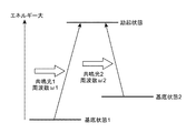
図3は、図1,2に示す原子発振器100の動作を示す概略構成図である。また、図4は、図1,2に示す原子発振器100のガスセル11内におけるアルカリ金属のエネルギー状態を説明するための図、図5は、図1,2に示す原子発振器100の光射出部20(光源22)および光検出部30について、光射出部20(光源22)からの2つの光の周波数差と、光検出部での検出強度との関係を示すグラフである。
FIG. 3 is a schematic configuration diagram showing an operation of the
先ず、原子発振器100の原理を簡単に説明する。原子発振器100では、ガスセル11内に、ガス状のルビジウム、セシウム、ナトリウム等のアルカリ金属(金属原子)が封入されている。アルカリ金属は、図4に示すように、3準位系のエネルギー準位を有しており、エネルギー準位の異なる2つの基底状態(基底状態1,2)と、励起状態との3つの状態をとり得る。ここで、基底状態1は、基底状態2よりも低いエネルギー状態である。
First, the principle of the
このようなガス状のアルカリ金属に対して周波数の異なる2種の共鳴光1、および共鳴光2を照射すると、共鳴光1の周波数ω1と共鳴光2の周波数ω2との差(ω1−ω2)に応じて、共鳴光1、および共鳴光2のアルカリ金属における光吸収率(光透過率)が変化する。そして、共鳴光1の周波数ω1と、共鳴光2の周波数ω2との差(ω1−ω2)が基底状態1と基底状態2とのエネルギー差に相当する周波数に一致したとき、基底状態1、および基底状態2から励起状態への励起がそれぞれ停止する。このとき、共鳴光1、および共鳴光2は、いずれも、アルカリ金属に吸収されずに透過する。このような現象をCPT(Coherent Population Trapping)現象、または電磁誘起透明化現象(EIT:Electromagnetically Induced Transparency)と呼ぶ。
When such a gaseous alkali metal is irradiated with two types of
光源22は、ガスセル11に向けて、前述したような周波数の異なる2種の光(共鳴光1および共鳴光2)を射出する。例えば、光源22が共鳴光1の周波数ω1を固定し、共鳴光2の周波数ω2を変化させていくと、共鳴光1の周波数ω1と共鳴光2の周波数ω2との差(ω1−ω2)が基底状態1と基底状態2とのエネルギー差に相当する周波数ω0に一致したとき、光検出部30の検出強度は、図5に示すように、急峻に上昇する。このような急峻な信号をEIT信号として検出する。このEIT信号は、アルカリ金属の種類によって決まった固有値をもっている。したがって、このようなEIT信号を用いることにより、発振器を構成することができる。
The
本実施形態に係る原子発振器100は、図3に示すように、光射出部20に備える光源22から、ガスセル11に向かって励起光LLがガスセル11への入射光として射出される。励起光LLとして、前述したように、周波数の異なる2種の光(共鳴光1および共鳴光2)が射出される。共鳴光1の周波数ω1は、ガスセル11中のアルカリ金属を前述した基底状態1から励起状態に励起し得るものである。また、共鳴光2の周波数ω2は、ガスセル11中のアルカリ金属を前述した基底状態2から励起状態に励起し得るものである。この光源22としては、前述したような励起光を射出し得るものであれば、特に限定されないが、例えば、垂直共振器面発光レーザー(VCSEL)等の半導体レーザー等を用いることができる。
In the
光射出部20から射出された励起光LLは、励起光LLの光軸方向R上のガスセル保持部材12に形成された貫通孔12aに設けられている光学部品14,15を透過する。光学部品14は、上述したようにλ/4波長板であり、光源22から射出された直線偏光の励起光LLを、円偏光(右偏光あるいは左偏光)に変換することができる。次に、光学部品15は、減光フィルター(NDフィルター)であり、ガスセル11に入射する励起光LLの強度を調整(減少)させることができ、光源22の出力が大きい場合でも、ガスセル11に入射する励起光LLを所望の光量とすることができる。
The excitation light LL emitted from the
光学部品14によって励起光LLが円偏光に変換されることによって、コイル13の磁場によりガスセル11内のアルカリ金属原子がゼーマン分裂した状態において、円偏光の励起光LLがアルカリ金属原子に照射されると、励起光LLとアルカリ金属原子との相互作用により、アルカリ金属原子がゼーマン分裂した複数の準位のうち、所望のエネルギー準位のアルカリ金属原子の数を他のエネルギー準位のアルカリ金属原子の数に対して相対的に多くすることができる。そのため、所望のEIT現象を発現する原子数が増大し、所望のEIT信号の強度が大きくなり、その結果、原子発振器100の発振特性を向上させることができる。
When the excitation light LL is converted into circularly polarized light by the
なお、光源22とガスセル11との間には、波長板および減光フィルターの他に、レンズ、偏光板等の他の光学部品が配置されていてもよい。また、光源22からの励起光LLの強度によっては、光学部品15を省略することができる。
Note that between the
ガスセル11内を透過した励起光LL(共鳴光1、共鳴光2)は、光検出部30により強度が検出される。励起光LLの光検出部30による検出結果は、制御部110(図1,2には図示されない)に備える励起光制御部111に入力され、光源22から射出される共鳴光1、共鳴光2の周波数を光検出部30の検出結果に基づいて制御する。より具体的には、励起光制御部111は、前述した光検出部30によって検出された(ω1−ω2)が前述したアルカリ金属固有の周波数ω0となるように、光源22から射出される共鳴光1、共鳴光2の周波数を制御する。また、励起光制御部111は、光源22から射出される共鳴光1、共鳴光2の中心周波数を制御する。これにより、前述したようなEIT信号を検出することができる。そして、制御部110は、図示しない水晶発振器の信号をEIT信号に同期して出力させる。
The intensity of the excitation light LL (
制御部110には、温度制御部112、および磁場制御部113を備えている。温度制御部112には、図1,2には図示されないガスセル11の温度を検出する温度センサー61からの計測検出結果に基づいて、ヒーター60への通電を制御し、ガスセル11を所望の温度範囲内に維持する。磁場制御部113は、コイル13が発生する磁場が一定となるように、コイル13への通電を制御する。そして、このような制御部110は、例えば、原子発振器100が実装される実装基板上に実装された電子回路装置(例えば、半導体装置)に設けられている。
The
図3に示す、制御部110に備える励起光制御部111から、光射出部20の光源22に励起光LLを射出させる高周波信号が、高周波信号伝導線114によって伝達される。図6は、図3に示す高周波信号伝導線114と、光源22と、の接続を模式的に示す概略断面図である。
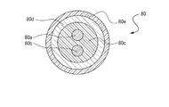
A high-frequency signal that causes the
図6に示すように、高周波信号伝導線114は、いわゆる同軸ケーブル80によって構成されている。図6に示す高周波信号伝導線としての同軸ケーブル80のB−B´部の断面を図7に示す。図7に示すように、同軸ケーブル80は、高周波信号を伝達する導電芯線80a,80b(以下、芯線80a、芯線80b)が、絶縁材料からなる芯線被覆部80cによって覆われ、芯線80aと、芯線80bと、が電気的に絶縁されている。
As shown in FIG. 6, the high-frequency signal
芯線被覆部80cの外周面を覆うように、導電材料によるシールド線80dが配置される。シールド線80dは、例えばアルミニウムの細線を網状に形成し、芯線被覆部80cを覆う、あるいはアルミ箔によって芯線被覆部80cを覆う、などの方法によって形成される。そしてシールド線80dの外周には外部との絶縁と保護のための絶縁保護部80eが被覆されている。絶縁保護部80eは、電気的な絶縁性を備え、水分、油分、高低温、などの外部環境への耐性を備える柔軟性を有する材料で形成される。
A
図6に示すように、同軸ケーブル80は図示しない励起光制御部111に接続され、図3に示す高周波信号伝導線114として、基板50の光源収容体21、およびガスセルユニット10を収容する第1磁気遮蔽体40などが配置される基板面50aに設置されたケーブル固定部90に固着される。
As shown in FIG. 6, the
同軸ケーブル80のケーブル固定部90での固定端部80fは、芯線80a,80bが露出され、基体部21aの外部に形成された外部接続電極21e,21fにそれぞれ電気的に接続される。外部接続電極21e,21fは、光源収容体21の内部に形成された内部配線によって内部接続電極21g,21hに電気的に接続されている。更に、内部接続電極21g,21hと、図示しない光源22の電極と、がボンディングワイヤー20a,20bによって電気的に接続されている。これにより、同軸ケーブル80の芯線80a,80bを通して励起光制御部111から出力された高周波信号が光源22に入力され、所定の励起光LLがガスセル11に向けて出射される。
The fixed ends 80f of the
この時、励起光制御部111において生成された高周波信号の伝導経路である同軸ケーブル80の芯線80a,80bから外部への高周波信号の漏れが生じることで、所定の高周波信号出力を光源22に入力することが困難となる。そこで、同軸ケーブル80は、シールド線80dを備えることにより、高周波信号の外部への漏れの抑制、防止をすることができる。
At this time, a predetermined high-frequency signal output is input to the
しかし、光源収容体21の基体部21aに形成された外部接続電極21e,21fと、同軸ケーブル80との電気的な接続においては、ケーブル固定部90に固定される側の同軸ケーブル80の固定端部80fから外部接続電極21e,21fまでの間、芯線80a,80bは同軸ケーブル80から露出される。従って、固定端部80fから外部接続電極21e,21fまでの間の露出した芯線80a,80bからは高周波信号が、芯線80a,80bの露出部を収容する第2磁気遮蔽体70の内部空間内に漏れる。加えて、外部接続電極21e,21fから光源22に至る各配線にも、高周波信号の遮蔽部材が配設されていない。
However, in the electrical connection between the
高周波信号の遮蔽部材が配設されていない領域が存在することにより、光源22に入力される高周波信号が漏れることで、第2磁気遮蔽体70の内部空間に、空間高周波の定在波SWが生じる。この定在波SWは、第2磁気遮蔽体70の第2蓋体71の内壁面の内、励起光LLの出射方向とは反対方向における光源22に最も近い第1壁面としての内壁面71aを起点とした空間高周波として発生する。そして、定在波SWのエネルギーは光源22に入力される高周波信号を減衰させるように作用し、励起光LLの安定した出射を阻害してしまう虞があった。
Since the high-frequency signal input to the
上述の芯線80a,80bが露出される固定端部80fから、励起光LLの射出方向に沿って遮蔽部材を備えない光源配線、すなわち露出された芯線80a,80bと、外部接続電極21e,21fと、内部接続電極21g,21hと、外部接続電極21e,21fと内部接続電極21g,21hとを電気的に接続する内部配線と、ボンディングワイヤー20a,20bと、が存在する平面視での領域を領域Q1(以下、光源配線領域Q1という)と定義する。
From the
ここで、上述の平面視とは、図6に示すX,Y,Z座標系において、X軸に交差する方向からの矢視を言い、本実施形態の説明では、Y軸方向に沿った矢視を平面視としている。 Here, the above-described planar view refers to an arrow viewed from a direction intersecting the X axis in the X, Y, and Z coordinate systems illustrated in FIG. 6, and in the description of the present embodiment, an arrow along the Y axis direction. The view is a planar view.
定在波SWにおいて、最大振幅Fmaxを示す位置を最大振幅点Pb(図示、×印点)、最少振幅点Ps(図示、●印点)とした場合、光源配線領域Q1の領域内に最大振幅点Pbが含まれないように、光源22を配置する。これにより、光源22に入力される高周波信号が遮蔽されていない領域、言い換えると空間高周波の影響を受けやすい光源配線領域Q1に、空間高周波のエネルギーピーク領域が重ならず、安定した高出力の高周波信号を光源22に入力させることができる。
In the standing wave SW, when the position indicating the maximum amplitude Fmax is the maximum amplitude point Pb (illustrated, x mark point) and the minimum amplitude point Ps (illustration, ● mark point), the maximum amplitude is within the light source wiring area Q1. The
更に、光源配線領域Q1の領域に最少振幅点Psが含まれるように、光源22を配置することがなお好ましい。これにより、光源22に入力される高周波信号が遮蔽されていない、言い換えると空間高周波の影響を受けやすい光源配線領域Q1には、空間高周波のエネルギーの最少領域となり、安定した高出力の高周波信号を光源22に入力させることができる。
Further, it is more preferable to arrange the
図8は、第2磁気遮蔽体70の内部領域での同軸ケーブル80の、その他の形態を示す断面図である。図8に示すように、第2磁気遮蔽体70の外部にケーブル固定部90が基板50の基板面50a上に配置され、同軸ケーブル80が基板50に対して固着される。そして、芯線80a,80bを内在する芯線被覆部80cが第2磁気遮蔽体70の内部に引き込まれる。第2磁気遮蔽体70の内部には、第2磁気遮蔽体70の内部に引き込まれた芯線被覆部80cに近接させて、シールド部91が配置される。
FIG. 8 is a cross-sectional view showing another form of the
シールド部91は、筒状に形成され、内部に芯線80a,80bを内在する芯線被覆部80cが挿通される。シールド部91は、第2磁気遮蔽体70の内部に光源22に入力される高周波信号の漏れをシールド部91から外側へ漏れ出すことを遮蔽する機能を有する。従って、シールド部91は、アルミニウム、銅、などの高周波の遮蔽性を有する材料によって形成される。
The
光源配線領域Q1は、図示するようにシールド部91の光源22側の端部91aから、励起光LLの射出方向に沿って遮蔽部材を備えない光源配線、すなわち露出された芯線80a,80bと、外部接続電極21e,21fと、内部接続電極21g,21hと、外部接続電極21e,21fと内部接続電極21g,21hとを電気的に接続する内部配線と、ボンディングワイヤー20a,20bと、が存在する平面視での領域となる。
The light source wiring region Q1 includes, as shown, a light source wiring having no shielding member from the
そして光源配線領域Q1の中に、空間高周波の定在波SWの最大振幅点Pbが含まれないように光源22が配置されることが好ましい。これにより、光源22に入力される高周波信号が遮蔽されていない、言い換えると空間高周波の影響を受けやすい光源配線領域Q1に、空間高周波のエネルギーピーク領域が重ならず、安定した高出力の高周波信号を光源22に入力させることができる。更には、光源配線領域Q1の領域に最少振幅点Psが含まれるように、光源22を配置することがなお好ましいい。これにより、光源22に入力される高周波信号が遮蔽されていない、言い換えると空間高周波の影響を受けやすい光源配線領域Q1には、空間高周波のエネルギーの最少領域となり、安定した高出力の高周波信号を光源22に入力させることができる。
Then, it is preferable that the
(第2実施形態)
第2実施形態として、第1実施形態に係る原子発振器100におけるガスセル11と、空間高周波の定在波SWとの関係を説明する。図9は、第1実施形態に係る原子発振器100を用いて、定在波SWとの関係を説明する断面図である。
(2nd Embodiment)
As a second embodiment, the relationship between the
図9に示すように、空間高周波の定在波SWは、第2磁気遮蔽体70の第2蓋体71の内壁面の内、励起光LLの出射方向とは反対方向における光源22に最も近い第1壁面としての内壁面71aを起点とした空間高周波として発生する。定在波SWのエネルギーはガスセル11の内部空間Sに収容されている金属原子に照射される励起光LLの強度を減衰させる虞があった。
As shown in FIG. 9, the standing wave SW of the spatial high frequency is closest to the
ここで、ガスセル11の内部空間Sにおける平面視での領域Q2(以下、ガスセル空間領域Q2という)と定義する。なお、平面視とは、図9に示すX,Y,Z座標系において、X軸に交差する方向からの矢視を言い、本実施形態の説明では、Y軸方向に沿った矢視を平面視としている。 Here, it is defined as a region Q2 in a plan view in the internal space S of the gas cell 11 (hereinafter, referred to as a gas cell space region Q2). Note that the plan view refers to an arrow viewed from a direction intersecting the X axis in the X, Y, and Z coordinate systems illustrated in FIG. 9. I am looking.
定在波SWにおいて、最大振幅Fmaxを示す位置を最大振幅点Pb(図示、×印点)、最少振幅点Ps(図示、●印点)とした場合、ガスセル空間領域Q2の領域内に最大振幅点Pbが含まれないように、ガスセル11を配置する。これにより、ガスセル11の内部空間Sのガスセル空間領域Q2の領域では、定在波SWによる励起光LLの強度への影響を抑制することができ、安定した発振性能を有する原子発振器100を得ることができる。
In the standing wave SW, when the position indicating the maximum amplitude Fmax is the maximum amplitude point Pb (illustrated, x mark point) and the minimum amplitude point Ps (illustration, ● mark point), the maximum amplitude is within the gas cell space area Q2. The
更に、ガスセル空間領域Q2の領域に最少振幅点Psが含まれるように、ガスセル11を配置することがなお好ましいい。これにより、ガスセル11の内部空間Sにおける励起光LLの強度への影響をより低減させることができ、安定した発振性能を有する原子発振器100を得ることができる。
Further, it is more preferable to arrange the
図10は、第2実施形態に係る原子発振器100のその他の形態として、本実施形態に係るガスセル11のガスセル空間領域Q2と、定在波SWの最大振幅点Pbと、の関係に加え、第1実施形態に係る光源配線領域Q1と、定在波SWの最大振幅点Pbと、の関係をも満足される形態を示す概略断面図である。
FIG. 10 shows, as another mode of the
図10に示すように、図9によって説明した本実施形態に係るガスセル11のガスセル空間領域Q2内に、定在波SWの最大振幅点Pbが含まれないガスセル11の配置となる原子発振器100である。これに加えて、図6によって説明した第1実施形態に係る光源配線領域Q1内に、定在波SWの最大振幅点Pbが含まれないように、光源22を配置する。
As shown in FIG. 10, the
このように、光源配線領域Q1と、ガスセル空間領域Q2と、に、定在波SWの最大振幅点Pbが含まれないように光源22と、ガスセル11と、を配置することにより、光源22に入力される高周波信号が遮蔽されていない領域、言い換えると空間高周波の影響を受けやすい光源配線領域Q1に、空間高周波のエネルギーピーク領域が重ならず、安定した高出力の高周波信号を光源22に入力させることができる。更に、ガスセル11の内部空間Sにおける励起光LLの強度への影響をより低減させることができ、安定した発振性能を有する原子発振器100を得ることができる。
Thus, by arranging the
(第3実施形態)
図11,12は、第3実施形態に係る原子発振器200を示し、図11は正断面図、図12は図11におけるC−C´部の断面図である。第3実施形態に係る原子発振器200は、第1実施形態、あるいは第2実施形態に係る原子発振器100に対して、第2磁気遮蔽体70の内部に誘電体が備えられている点で異なり、その他の構成要素は同じであるので、同じ構成要素には同じ符号を付し、説明は省略する。
(Third embodiment)
11 and 12 show an
図11、および図12に示すように本実施形態に係る原子発振器200は、第2磁気遮蔽体70の内部に、光射出部20と、第1磁気遮蔽体40に収容されたガスセルユニット10と、を備え、更に誘電体210が備えられている。
As shown in FIGS. 11 and 12, the
誘電体210は、例えばプラスチックあるいはセラミックなどが知られているが、特に限定は無く、第2磁気遮蔽体70の内部に発生する空間高周波の定在波SWの波長が短縮される物であればよい。また、本実施形態に係る誘電体210は、図13に示す形態を有している。なお、図13は誘電体210の外観斜視図であり、基板50の基板面50aに配置された状態の誘電体210だけを描画した図である。図13に示すように誘電体210は、基板50の基板面50aに、例えば接着剤によって固定されている。そして、励起光LLが通過できる切欠き210aが形成されている。
As the dielectric 210, for example, plastic or ceramic is known, but there is no particular limitation, as long as the wavelength of the spatial high-frequency standing wave SW generated inside the second
誘電体210は、図11,12に示すように第2磁気遮蔽体70の内部に収容され、本実施形態では、光射出部20と、ガスセルユニット10が収容された第1磁気遮蔽体40と、の間に配置され、光源22に入力される高周波信号によって発生する空間高周波の定在波SW(図6,8,9参照)の波長を、誘電体210の有する誘電性によって短縮させ、定在波SWの波長を変換する。これにより、定在波SWの最大振幅点Pbの位置を変えることができ、光源22あるいはガスセル11の配置位置の自由度を高めることができる。
The dielectric 210 is housed inside the second
なお、図14は、誘電体210のその他の形態の一例を示す外観斜視図である。図14に示すように、誘電体220は、複数の誘電体220a,220bであってもよく、励起光LLの光路を妨げず、第2磁気遮蔽体70の内部に収容されていればよい。
FIG. 14 is an external perspective view illustrating an example of another form of the dielectric 210. As shown in FIG. 14, the dielectric 220 may be a plurality of
(第4実施形態)
第4実施形態として、第1実施形態あるいは第2実施形態に係る原子発振器100、もしくは第3実施形態に係る原子発振器200のいずれかを備える電子機器の一例としてGPS衛星を利用した測位システムを説明する。図15は、GPS衛星を利用した測位システムに本発明に係る原子発振器を用いた場合の概略構成を示す図である。なお、本実施形態では第1実施形態に係る原子発振器100を備える形態を説明する。
(Fourth embodiment)
As a fourth embodiment, a positioning system using a GPS satellite will be described as an example of an electronic apparatus including one of the
図15に示す測位システム1000は、GPS衛星1100と、基地局装置1200と、GPS受信装置1300とで構成されている。GPS衛星1100は、測位情報(GPS信号)を送信する。基地局装置1200は、例えば電子基準点(GPS連続観測局)に設置されたアンテナ1201を介してGPS衛星1100からの測位情報を高精度に受信する受信装置1202と、この受信装置1202で受信した測位情報を、アンテナ1203を介して送信する送信装置1204とを備える。
The
ここで、受信装置1202は、その基準周波数発振源として前述した本発明に係る第1実施形態の原子発振器100を備える電子装置である。このような受信装置1202は、優れた信頼性を有する。また、受信装置1202で受信された測位情報は、リアルタイムで送信装置1204により送信される。GPS受信装置1300は、GPS衛星1100からの測位情報を、アンテナ1301を介して受信する衛星受信部1302と、基地局装置1200からの測位情報を、アンテナ1303を介して受信する基地局受信部1304とを備える。
Here, the
(第5実施形態)
第5実施形態として、第1実施形態あるいは第2実施形態に係る原子発振器100、もしくは第3実施形態に係る原子発振器200のいずれかを備える電子機器の一例としてクロック伝送システムを説明する。図16は、クロック伝送システムに本発明に係る原子発振器を用いた場合の概略構成を示す図である。なお、本実施形態では第1実施形態に係る原子発振器100を備える形態を説明する。
(Fifth embodiment)
As a fifth embodiment, a clock transmission system will be described as an example of an electronic apparatus including any one of the
図16に示すクロック伝送システム2000は、時分割多重方式のネットワーク内の各装置のクロックを一致させるものであって、N(Normal)系およびE(Emergency)系の冗長構成を有するシステムである。
A
このクロック伝送システム2000は、A局(上位(N系))のクロック供給装置(CSM:Clock Supply Module)2001およびSDH(Synchronous Digital Hierarchy)装置2002と、B局(上位(E系))のクロック供給装置2003およびSDH装置2004と、C局(下位)のクロック供給装置2005およびSDH装置2006,2007とを備える。クロック供給装置2001は、原子発振器100を有し、N系のクロック信号を生成する。このクロック供給装置2001内の原子発振器100は、セシウムを用いた原子発振器を含むマスタークロック2008,2009からのより高精度なクロック信号と同期して、クロック信号を生成する。
The
SDH装置2002は、クロック供給装置2001からのクロック信号に基づいて、主信号の送受信を行うとともに、N系のクロック信号を主信号に重畳し、下位のクロック供給装置2005に伝送する。クロック供給装置2003は、原子発振器100を有し、E系のクロック信号を生成する。このクロック供給装置2003内の原子発振器100は、セシウムを用いた原子発振器を含むマスタークロック2008,2009からのより高精度なクロック信号と同期して、クロック信号を生成する。
The
SDH装置2004は、クロック供給装置2003からのクロック信号に基づいて、主信号の送受信を行うとともに、E系のクロック信号を主信号に重畳し、下位のクロック供給装置2005に伝送する。クロック供給装置2005は、クロック供給装置2001,2003からのクロック信号を受信し、その受信したクロック信号に同期して、クロック信号を生成する。
The
ここで、クロック供給装置2005は、通常、クロック供給装置2001からのN系のクロック信号に同期して、クロック信号を生成する。そして、N系に異常が発生した場合、クロック供給装置2005は、クロック供給装置2003からのE系のクロック信号に同期して、クロック信号を生成する。このようにN系からE系に切り換えることにより、安定したクロック供給を担保し、クロックパス網の信頼性を高めることができる。SDH装置2006は、クロック供給装置2005からのクロック信号に基づいて、主信号の送受信を行う。同様に、SDH装置2007は、クロック供給装置2005からのクロック信号に基づいて、主信号の送受信を行う。これにより、C局の装置をA局またはB局の装置と同期させることができる。
Here, the
(第6実施形態)
第6実施形態として、第1実施形態あるいは第2実施形態に係る原子発振器100、もしくは第3実施形態に係る原子発振器200のいずれかを備える移動体の一例として自動車を例に説明する。図17は、移動体としての自動車に本発明に係る原子発振器を用いた場合の概略構成を示す斜視図である。なお、本実施形態では第1実施形態に係る原子発振器100を備える形態を説明する。
(Sixth embodiment)
As a sixth embodiment, an automobile will be described as an example of a moving object including either the
図17に示す移動体としての自動車3000は、車体3001と、4つの車輪3002とを有しており、車体3001に設けられた図示しない動力源によって車輪3002を回転させるように構成されている。このような自動車3000には、原子発振器100が内蔵されている。そして、原子発振器100からの発振信号に基づいて、例えば、図示しない制御部が動力源の駆動を制御する。
An
なお、本発明の原子発振器を組み込む電子機器または移動体は、前述したものに限定されず、例えば、携帯電話機、デジタルスチールカメラ、インクジェット式吐出装置(例えばインクジェットプリンター)、パーソナルコンピューター(モバイル型パーソナルコンピューター、ラップトップ型パーソナルコンピューター)、テレビ、ビデオカメラ、ビデオテープレコーダー、カーナビゲーション装置、ページャー、電子手帳(通信機能付も含む)、電子辞書、電卓、電子ゲーム機器、ワードプロセッサー、ワークステーション、テレビ電話、防犯用テレビモニター、電子双眼鏡、POS端末、医療機器(例えば電子体温計、血圧計、血糖計、心電図計測装置、超音波診断装置、電子内視鏡)、魚群探知機、各種測定機器、計器類(例えば、車両、航空機、船舶の計器類)、フライトシミュレーター等に適用することができる。 Note that the electronic device or moving object incorporating the atomic oscillator of the present invention is not limited to those described above, and includes, for example, a mobile phone, a digital still camera, an ink jet type ejection device (eg, an ink jet printer), and a personal computer (mobile personal computer). , Laptop personal computers), televisions, video cameras, video tape recorders, car navigation systems, pagers, electronic organizers (including those with communication functions), electronic dictionaries, calculators, electronic game machines, word processors, workstations, videophones, Security TV monitor, electronic binoculars, POS terminal, medical equipment (for example, electronic thermometer, sphygmomanometer, blood glucose meter, electrocardiogram measuring device, ultrasonic diagnostic device, electronic endoscope), fish finder, various measuring devices, instruments ( For example, Two, aircraft, gauges of a ship), can be applied to a flight simulator or the like.
以上、本発明の原子発振器について、図示の実施形態に基づいて説明したが、本発明は、これらに限定されるものではなく、例えば、前述した実施形態の各部の構成は、同様の機能を発揮する任意の構成のものに置換することができ、また、任意の構成を付加することもできる。また、本発明は、前述した各実施形態の任意の構成同士を組み合わせるようにしてもよい。 As described above, the atomic oscillator of the present invention has been described based on the illustrated embodiments. However, the present invention is not limited to these. For example, the configuration of each unit of the above-described embodiment exhibits the same function. It can be replaced with an arbitrary configuration, or an arbitrary configuration can be added. In addition, the present invention may be configured to combine arbitrary configurations of the embodiments described above.
11…ガスセル、20…光射出部、40…第1磁気遮蔽体、50…基板、70…第2磁気遮蔽体、80…同軸ケーブル、100…原子発振器。 11: gas cell, 20: light emitting unit, 40: first magnetic shield, 50: substrate, 70: second magnetic shield, 80: coaxial cable, 100: atomic oscillator.
Claims (4)
高周波信号を生成する励起光制御部と、
前記高周波信号が入力され、前記ガスセルに励起光を射出するレーザー光源と、
前記ガスセルおよび前記レーザー光源を収容する収容体と、
前記高周波信号を導通する芯線と、前記芯線から漏れる前記高周波信号を遮蔽するシールド部と、を有し、前記レーザー光源と前記励起光制御部とを電気的に接続する高周波信号伝導線と、
前記芯線と、前記レーザー光源と、を電気的に接続する接続配線と、
を含み、
前記励起光の射出方向において、前記芯線の前記シールド部から露出する部分、および、前記接続配線が存在する領域を光源配線領域とし、
前記射出方向と反対方向で、前記レーザー光源に最も近い前記収容体の内壁面を第1壁面とした場合に、
前記高周波信号により発生する空間高周波の定在波は、前記第1壁面に起点を有し、
前記射出方向において、前記光源配線領域は、前記定在波の最大振幅点を含まない、
原子発振器。 A gas cell containing metal atoms,
An excitation light control unit that generates a high-frequency signal,
A laser light source that receives the high-frequency signal and emits excitation light to the gas cell,
A housing that houses the gas cell and the laser light source,
A core wire that conducts the high-frequency signal, and a shield portion that shields the high-frequency signal leaking from the core wire, and a high-frequency signal conductive line that electrically connects the laser light source and the excitation light control unit,
The core wire and the laser light source, a connection wiring for electrically connecting,
Including
In the emission direction of the excitation light, a portion of the core wire exposed from the shield portion, and a region where the connection wiring exists as a light source wiring region,
In the opposite direction to the emission direction, when the inner wall surface of the container closest to the laser light source is the first wall surface,
The spatial high-frequency standing wave generated by the high-frequency signal has a starting point on the first wall surface,
In the emission direction, the light source wiring region does not include a maximum amplitude point of the standing wave,
Atomic oscillator.
高周波信号が入力され、前記ガスセルに励起光を射出するレーザー光源と、
前記ガスセルと、前記レーザー光源と、を収容する収容体と、
を含み、
前記励起光の射出方向と反対方向で、前記レーザー光源に最も近い前記収容体の内壁面を第1壁面とした場合に、
前記高周波信号により発生する空間高周波の定在波は、前記第1壁面に起点を有し、
前記射出方向において、前記ガスセルの前記金属原子が封入される収容部は、前記定在波の最大振幅点を含まない、
原子発振器。 A gas cell containing metal atoms,
A high frequency signal is input, a laser light source that emits excitation light to the gas cell,
The gas cell, and a housing for housing the laser light source,
Including
In the direction opposite to the emission direction of the excitation light, when the inner wall surface of the container closest to the laser light source is the first wall surface,
The spatial high-frequency standing wave generated by the high-frequency signal has a starting point on the first wall surface,
In the emission direction, the housing section in which the metal atoms of the gas cell are sealed does not include a maximum amplitude point of the standing wave,
Atomic oscillator.
請求項1に記載の原子発振器。 In the emission direction, the housing section in which the metal atoms of the gas cell are sealed does not include a maximum amplitude point of the standing wave,
The atomic oscillator according to claim 1.
請求項1乃至請求項3のいずれか一項に記載の原子発振器。 Including a dielectric for wavelength conversion disposed between the laser light source and the gas cell ,
The atomic oscillator according to claim 1.
Priority Applications (1)
| Application Number | Priority Date | Filing Date | Title |
|---|---|---|---|
| JP2015222778A JP6661985B2 (en) | 2015-11-13 | 2015-11-13 | Atomic oscillator |
Applications Claiming Priority (1)
| Application Number | Priority Date | Filing Date | Title |
|---|---|---|---|
| JP2015222778A JP6661985B2 (en) | 2015-11-13 | 2015-11-13 | Atomic oscillator |
Publications (3)
| Publication Number | Publication Date |
|---|---|
| JP2017092797A JP2017092797A (en) | 2017-05-25 |
| JP2017092797A5 JP2017092797A5 (en) | 2018-11-22 |
| JP6661985B2 true JP6661985B2 (en) | 2020-03-11 |
Family
ID=58771765
Family Applications (1)
| Application Number | Title | Priority Date | Filing Date |
|---|---|---|---|
| JP2015222778A Active JP6661985B2 (en) | 2015-11-13 | 2015-11-13 | Atomic oscillator |
Country Status (1)
| Country | Link |
|---|---|
| JP (1) | JP6661985B2 (en) |
Families Citing this family (1)
| Publication number | Priority date | Publication date | Assignee | Title |
|---|---|---|---|---|
| CN112702060A (en) * | 2020-12-11 | 2021-04-23 | 兰州空间技术物理研究所 | Microwave amplitude control method for cesium atomic clock |
Family Cites Families (4)
| Publication number | Priority date | Publication date | Assignee | Title |
|---|---|---|---|---|
| JP4599091B2 (en) * | 2004-05-19 | 2010-12-15 | 日本オプネクスト株式会社 | Optical module and optical transmission device |
| JP2007088538A (en) * | 2005-09-20 | 2007-04-05 | Epson Toyocom Corp | Rubidium atomic oscillator |
| JP2011222866A (en) * | 2010-04-13 | 2011-11-04 | Mitsubishi Electric Corp | High-frequency package and manufacturing method thereof |
| JP2014183484A (en) * | 2013-03-19 | 2014-09-29 | Seiko Epson Corp | Electronic device, quantum interference device, atomic oscillator, electronic apparatus, mobile body, and method of manufacturing electronic device |
-
2015
- 2015-11-13 JP JP2015222778A patent/JP6661985B2/en active Active
Also Published As
| Publication number | Publication date |
|---|---|
| JP2017092797A (en) | 2017-05-25 |
Similar Documents
| Publication | Publication Date | Title |
|---|---|---|
| JP6119295B2 (en) | Quantum interference device, atomic oscillator, and moving object | |
| JP6354151B2 (en) | Quantum interference devices, atomic oscillators, electronic equipment, and moving objects | |
| US9912339B2 (en) | Atomic oscillator | |
| JP6119294B2 (en) | Quantum interference device, atomic oscillator, and moving object | |
| US10396810B2 (en) | Quantum interference device, atomic oscillator, electronic apparatus, and moving object | |
| JP6179327B2 (en) | Quantum interference devices, atomic oscillators, electronic equipment, and moving objects | |
| JP6627334B2 (en) | Atomic oscillators and electronics | |
| JP6627349B2 (en) | Atomic oscillator | |
| JP2017092796A (en) | Atomic oscillator and temperature control method for the same | |
| JP2015118962A (en) | Quantum interference device, atomic oscillator, electronic apparatus and mobile body | |
| JP6263869B2 (en) | Atomic oscillator and electronic equipment | |
| JP6763135B2 (en) | Atomic oscillator | |
| JP2014183484A (en) | Electronic device, quantum interference device, atomic oscillator, electronic apparatus, mobile body, and method of manufacturing electronic device | |
| JP6728850B2 (en) | Quantum interference device, atomic oscillator and electronic equipment | |
| JP2019080287A (en) | Frequency signal generator and frequency signal generation system | |
| JP2017183869A (en) | Quantum interference device, atomic oscillator, electronic apparatus and mobile | |
| JP6337456B2 (en) | Quantum interference devices, atomic oscillators, electronic equipment, and moving objects | |
| JP6661985B2 (en) | Atomic oscillator | |
| JP6337464B2 (en) | Quantum interference devices, atomic oscillators, and electronic equipment | |
| US10432204B2 (en) | Atomic oscillator | |
| JP2015170882A (en) | Oscillator, electronic apparatus and moving body | |
| JP2020162054A (en) | Atomic oscillator and frequency signal generation system | |
| JP2020141342A (en) | Atomic oscillator and frequency signal generation system | |
| JP2017135529A (en) | Atomic oscillator | |
| JP2014160978A (en) | Quantum interference device, atomic oscillator, electronic apparatus and mobile body |
Legal Events
| Date | Code | Title | Description |
|---|---|---|---|
| RD05 | Notification of revocation of power of attorney |
Free format text: JAPANESE INTERMEDIATE CODE: A7425 Effective date: 20180906 |
|
| A521 | Request for written amendment filed |
Free format text: JAPANESE INTERMEDIATE CODE: A523 Effective date: 20181011 |
|
| A621 | Written request for application examination |
Free format text: JAPANESE INTERMEDIATE CODE: A621 Effective date: 20181011 |
|
| RD03 | Notification of appointment of power of attorney |
Free format text: JAPANESE INTERMEDIATE CODE: A7423 Effective date: 20181116 |
|
| A977 | Report on retrieval |
Free format text: JAPANESE INTERMEDIATE CODE: A971007 Effective date: 20190731 |
|
| A131 | Notification of reasons for refusal |
Free format text: JAPANESE INTERMEDIATE CODE: A131 Effective date: 20190806 |
|
| A521 | Request for written amendment filed |
Free format text: JAPANESE INTERMEDIATE CODE: A523 Effective date: 20191003 |
|
| TRDD | Decision of grant or rejection written | ||
| A01 | Written decision to grant a patent or to grant a registration (utility model) |
Free format text: JAPANESE INTERMEDIATE CODE: A01 Effective date: 20200114 |
|
| A61 | First payment of annual fees (during grant procedure) |
Free format text: JAPANESE INTERMEDIATE CODE: A61 Effective date: 20200127 |
|
| R150 | Certificate of patent or registration of utility model |
Ref document number: 6661985 Country of ref document: JP Free format text: JAPANESE INTERMEDIATE CODE: R150 |
|
| S111 | Request for change of ownership or part of ownership |
Free format text: JAPANESE INTERMEDIATE CODE: R313113 |
|
| R350 | Written notification of registration of transfer |
Free format text: JAPANESE INTERMEDIATE CODE: R350 |
|
| R250 | Receipt of annual fees |
Free format text: JAPANESE INTERMEDIATE CODE: R250 |
|
| R250 | Receipt of annual fees |
Free format text: JAPANESE INTERMEDIATE CODE: R250 |