JP6655152B2 - Bus protocol for dynamic lighting applications - Google Patents
Bus protocol for dynamic lighting applications Download PDFInfo
- Publication number
- JP6655152B2 JP6655152B2 JP2018202738A JP2018202738A JP6655152B2 JP 6655152 B2 JP6655152 B2 JP 6655152B2 JP 2018202738 A JP2018202738 A JP 2018202738A JP 2018202738 A JP2018202738 A JP 2018202738A JP 6655152 B2 JP6655152 B2 JP 6655152B2
- Authority
- JP
- Japan
- Prior art keywords
- unit
- data
- bit
- field
- drive unit
- Prior art date
- Legal status (The legal status is an assumption and is not a legal conclusion. Google has not performed a legal analysis and makes no representation as to the accuracy of the status listed.)
- Active
Links
Images


Classifications
-
- H—ELECTRICITY
- H05—ELECTRIC TECHNIQUES NOT OTHERWISE PROVIDED FOR
- H05B—ELECTRIC HEATING; ELECTRIC LIGHT SOURCES NOT OTHERWISE PROVIDED FOR; CIRCUIT ARRANGEMENTS FOR ELECTRIC LIGHT SOURCES, IN GENERAL
- H05B45/00—Circuit arrangements for operating light-emitting diodes [LED]
-
- G—PHYSICS
- G06—COMPUTING OR CALCULATING; COUNTING
- G06F—ELECTRIC DIGITAL DATA PROCESSING
- G06F13/00—Interconnection of, or transfer of information or other signals between, memories, input/output devices or central processing units
- G06F13/38—Information transfer, e.g. on bus
-
- H—ELECTRICITY
- H04—ELECTRIC COMMUNICATION TECHNIQUE
- H04L—TRANSMISSION OF DIGITAL INFORMATION, e.g. TELEGRAPHIC COMMUNICATION
- H04L1/00—Arrangements for detecting or preventing errors in the information received
- H04L1/004—Arrangements for detecting or preventing errors in the information received by using forward error control
-
- H—ELECTRICITY
- H05—ELECTRIC TECHNIQUES NOT OTHERWISE PROVIDED FOR
- H05B—ELECTRIC HEATING; ELECTRIC LIGHT SOURCES NOT OTHERWISE PROVIDED FOR; CIRCUIT ARRANGEMENTS FOR ELECTRIC LIGHT SOURCES, IN GENERAL
- H05B47/00—Circuit arrangements for operating light sources in general, i.e. where the type of light source is not relevant
- H05B47/10—Controlling the light source
- H05B47/175—Controlling the light source by remote control
- H05B47/18—Controlling the light source by remote control via data-bus transmission
-
- B—PERFORMING OPERATIONS; TRANSPORTING
- B60—VEHICLES IN GENERAL
- B60Q—ARRANGEMENT OF SIGNALLING OR LIGHTING DEVICES, THE MOUNTING OR SUPPORTING THEREOF OR CIRCUITS THEREFOR, FOR VEHICLES IN GENERAL
- B60Q1/00—Arrangement of optical signalling or lighting devices, the mounting or supporting thereof or circuits therefor
-
- B—PERFORMING OPERATIONS; TRANSPORTING
- B60—VEHICLES IN GENERAL
- B60R—VEHICLES, VEHICLE FITTINGS, OR VEHICLE PARTS, NOT OTHERWISE PROVIDED FOR
- B60R16/00—Electric or fluid circuits specially adapted for vehicles and not otherwise provided for; Arrangement of elements of electric or fluid circuits specially adapted for vehicles and not otherwise provided for
- B60R16/02—Electric or fluid circuits specially adapted for vehicles and not otherwise provided for; Arrangement of elements of electric or fluid circuits specially adapted for vehicles and not otherwise provided for electric constitutive elements
- B60R16/023—Electric or fluid circuits specially adapted for vehicles and not otherwise provided for; Arrangement of elements of electric or fluid circuits specially adapted for vehicles and not otherwise provided for electric constitutive elements for transmission of signals between vehicle parts or subsystems
- B60R16/0238—Electrical distribution centers
-
- H—ELECTRICITY
- H04—ELECTRIC COMMUNICATION TECHNIQUE
- H04L—TRANSMISSION OF DIGITAL INFORMATION, e.g. TELEGRAPHIC COMMUNICATION
- H04L12/00—Data switching networks
- H04L12/28—Data switching networks characterised by path configuration, e.g. LAN [Local Area Networks] or WAN [Wide Area Networks]
- H04L12/40—Bus networks
- H04L2012/40267—Bus for use in transportation systems
- H04L2012/40273—Bus for use in transportation systems the transportation system being a vehicle
-
- H—ELECTRICITY
- H04—ELECTRIC COMMUNICATION TECHNIQUE
- H04L—TRANSMISSION OF DIGITAL INFORMATION, e.g. TELEGRAPHIC COMMUNICATION
- H04L67/00—Network arrangements or protocols for supporting network services or applications
- H04L67/01—Protocols
- H04L67/12—Protocols specially adapted for proprietary or special-purpose networking environments, e.g. medical networks, sensor networks, networks in vehicles or remote metering networks
-
- H—ELECTRICITY
- H05—ELECTRIC TECHNIQUES NOT OTHERWISE PROVIDED FOR
- H05B—ELECTRIC HEATING; ELECTRIC LIGHT SOURCES NOT OTHERWISE PROVIDED FOR; CIRCUIT ARRANGEMENTS FOR ELECTRIC LIGHT SOURCES, IN GENERAL
- H05B45/00—Circuit arrangements for operating light-emitting diodes [LED]
- H05B45/30—Driver circuits
- H05B45/32—Pulse-control circuits
- H05B45/325—Pulse-width modulation [PWM]
-
- H—ELECTRICITY
- H05—ELECTRIC TECHNIQUES NOT OTHERWISE PROVIDED FOR
- H05B—ELECTRIC HEATING; ELECTRIC LIGHT SOURCES NOT OTHERWISE PROVIDED FOR; CIRCUIT ARRANGEMENTS FOR ELECTRIC LIGHT SOURCES, IN GENERAL
- H05B47/00—Circuit arrangements for operating light sources in general, i.e. where the type of light source is not relevant
- H05B47/10—Controlling the light source
- H05B47/175—Controlling the light source by remote control
- H05B47/198—Grouping of control procedures or address assignation to light sources
Landscapes
- Engineering & Computer Science (AREA)
- Theoretical Computer Science (AREA)
- Physics & Mathematics (AREA)
- General Engineering & Computer Science (AREA)
- General Physics & Mathematics (AREA)
- Computer Networks & Wireless Communication (AREA)
- Signal Processing (AREA)
- Circuit Arrangement For Electric Light Sources In General (AREA)
- Small-Scale Networks (AREA)
Description
本発明は、イルミネーションおよび信号伝達システムの分野に関する。より具体的には、本発明は、データ送信を介したLEDクラスタの制御に関する。 The present invention relates to the field of illumination and signaling systems. More specifically, the present invention relates to controlling LED clusters via data transmission.
イルミネーションシステムは、とりわけ自動車の照明用途のためのものであって、LED技術を使用することが多い。LEDイルミネーション源の製造は安価であり、LEDイルミネーション源のエネルギー消費は低いので、LED技術を使用するのが通常は有利である。 Illumination systems are especially for automotive lighting applications and often use LED technology. It is usually advantageous to use LED technology because the manufacture of LED illumination sources is inexpensive and the energy consumption of LED illumination sources is low.
自動車用途におけるイルミネーションシステムの制御は、堅固で耐故障性であるべきである。例えば、それは、外部電界、電気的ピークまたは他のノイズ源によって影響されるべきではない。しかしながら、自動車環境は電気的なイズが多い。欠陥のあるデータの送信、またはイルミネーションシステムの意図しない起動は、避けるべき危険な状況につながる可能性がある。 The control of the illumination system in automotive applications should be robust and fault-tolerant. For example, it should not be affected by external electric fields, electrical peaks or other noise sources. However, the vehicle environment has many electrical noises. Transmission of defective data or unintentional activation of the illumination system can lead to dangerous situations to be avoided.
既存のシステムは、通常、LINまたはCANシステムによる異なるLEDと、それらのコントローラとの間の接続を提供する。LINの場合、制御可能なLEDの数は非常に限られている。一方、イルミネーションシステムをCANに直接設定することは複雑であり、故障または事故の場合には修理または交換が困難であり、実装は高価である。 Existing systems typically provide a connection between different LEDs via a LIN or CAN system and their controllers. In the case of LIN, the number of controllable LEDs is very limited. On the other hand, setting the illumination system directly on the CAN is complex, difficult to repair or replace in case of failure or accident, and expensive to implement.
さらに、既存の実装は、例えば干渉、静電気放電またはアンテナ効果に起因するエラーを起こしやすい。これらの影響を低減するために、特許文献1は、例えば電力線の影響または外部の影響に起因するアンテナ効果の影響を低減するSPIまたは単方向差動データバスに基づく実装を開示している。しかしながら、この保護は部分的なものに過ぎず、LEDコントローラのばらつきまたは不規則性に起因する保護はできない。 In addition, existing implementations are prone to errors due to, for example, interference, electrostatic discharge or antenna effects. In order to reduce these effects, US Pat. No. 6,077,086 discloses an implementation based on SPI or a unidirectional differential data bus, for example, that reduces the effects of antenna effects due to power line effects or external effects. However, this protection is only partial and cannot be provided due to variations or irregularities in the LED controller.
本発明の実施形態の目的は、電子デバイスに給電するための命令の堅固な送信のための柔軟な通信ネットワークを提供するイルミネーションのためのシステム、バスプロトコル、および自動アドレス指定方法を提供することである。本発明の実施形態の利点は、診断情報の送信のために柔軟な通信ネットワークが得られ、データ送信が、データ送信の1つ以上の段階で望ましくない変化を含んでいなかったことのチェックを含むことである。 It is an object of embodiments of the present invention to provide a system for illumination, a bus protocol, and an automatic addressing method that provides a flexible communication network for robust transmission of instructions for powering electronic devices. is there. An advantage of embodiments of the present invention is that a flexible communication network is provided for the transmission of diagnostic information, and a check is made that the data transmission did not include undesired changes in one or more stages of the data transmission. It is to include.
本発明は、電子ユニットに給電するための複数の駆動ユニットを動作させる方法であって、本方法は、ビットシーケンスを含むデータフレームを、マスタ制御ユニットと、スレーブノードにおける複数の駆動ユニットのうちの少なくとも1つとの間で交換することを含み、シーケンスが、連続するビット列のフィールドの中で分割されており、本方法は、
マスタ制御ユニットと、少なくとも1つのアドレス指定された駆動ユニットとの間でデータを交換するために、少なくとも1つの駆動ユニットをアドレス指定するためのIDフィールドを適用することと、
電子ユニットの状態に関する情報および/または命令を含むデータフィールドを適用することと、を含み、
IDフィールドを適用することが、
Nビットを含む第1のビット部分列を使用して駆動ユニットにアドレスを示すことであって、アドレス指定された駆動ユニットにデータフィールドを適用するか、または駆動ユニットがアドレス指定されていない場合にはデータフィールドを無視するために、2Nが複数の駆動ユニットにおける駆動ユニットの数と等しいかまたはそれよりも多い、示すことと、
データが駆動ユニットから受信されるべきか、もしくは駆動ユニットに送信されるべきかを、マスタ制御ユニットが識別することを可能にするか、または、受信/送信(R/T)コマンドビットに割り当てられた値に依存して、どのアクションがマスタ制御ユニットによって要求されるかを各アドレス指定された駆動ユニットが解読することを可能にするため、値を割り当てるために受信/送信コマンドビットを使用することと、
データフレームに含まれる命令のタイプに関するIDフィールドにおける情報を含むさらなる機能ビットを使用することと、
機能ビットに割り当てられた値に依存して、第2のビット部分列内のデータビットを異なる電子ユニットに割り当てるか、またはその第2のビット部分列を使用してデータフィールド内のビット列の長さを示すための長さ解読ステップを実行することと、をさらに含むことを特徴とする。
The present invention is a method of operating a plurality of drive units for powering an electronic unit, the method comprising the steps of: transmitting a data frame including a bit sequence to a master control unit and a plurality of drive units in a slave node. Including exchanging with at least one of the sequences, wherein the sequence is divided into fields of a contiguous bit sequence;
Applying an ID field for addressing at least one drive unit to exchange data between the master control unit and at least one addressed drive unit;
Applying a data field containing information and / or instructions regarding the status of the electronic unit;
Applying the ID field
Indicating an address to a drive unit using a first bit subsequence including N bits, either applying a data field to the addressed drive unit, or if the drive unit is not addressed Indicates that 2 N is equal to or greater than the number of drive units in the plurality of drive units to ignore the data field;
Allows the master control unit to identify whether data is to be received from or transmitted to the drive unit, or is assigned to a receive / transmit (R / T) command bit. Using receive / transmit command bits to assign a value to allow each addressed drive unit to decode which action is required by the master control unit, depending on the value When,
Using an additional function bit that includes information in the ID field regarding the type of instruction included in the data frame;
Depending on the value assigned to the function bit, either assign the data bits in the second bit subsequence to a different electronic unit, or use the second bit subsequence to determine the length of the bit sequence in the data field And performing a length decoding step to indicate
本発明の実施形態の利点は、特定の駆動ユニットのアドレス指定を含む、MCUと複数の駆動ユニットの各々との間で、予測可能なビットシーケンス長を有する高速かつ堅固な通信を同時に設定することができることである。本発明の実施形態の利点は、多数のスレーブノードを、例えば60個のスレーブノードまでをアドレス指定することができることである。本発明の実施形態の利点は、差動バスを使用できることである。本発明の実施形態の利点は、高速なシステムが得られることである。例えば、いくつかの用途では、最大750キロボー(kBaud)までの速度が得られ、電子ユニットの更新サイクルは10msになる。言及された電子ユニットはLEDであってもよいが、本発明の実施形態はこれに限定されず、ユニットは、例えば、任意のタイプの照明デバイスであってもよく、さらに一般的には、給電される必要がある任意のタイプの電子デバイスであってもよい。 An advantage of embodiments of the present invention is that simultaneously setting up a fast and robust communication with a predictable bit sequence length between the MCU and each of the plurality of drive units, including the addressing of a particular drive unit. Is what you can do. An advantage of embodiments of the present invention is that multiple slave nodes can be addressed, for example, up to 60 slave nodes. An advantage of embodiments of the present invention is that a differential bus can be used. An advantage of embodiments of the present invention is that a fast system is obtained. For example, in some applications, speeds up to 750 kilobauds (kBaud) are obtained, and the update cycle of the electronic unit is 10 ms. The electronic unit mentioned may be an LED, but embodiments of the present invention are not limited thereto, and the unit may be, for example, any type of lighting device, and more generally It may be any type of electronic device that needs to be done.
本方法は、IDフィールドおよびデータフィールドのいかなる意図しない変更も検出するための巡回冗長性チェックをさらに含み得る。 The method may further include a cyclic redundancy check to detect any unintended changes in the ID and data fields.
本発明の実施形態の利点は、自動車環境では特に重要なバスプロトコルのレベルで、送信されるデータのノイズおよび偶発的なビット変動に対する強い保護が得られることである。 An advantage of an embodiment of the present invention is that it provides strong protection against noise and accidental bit fluctuations in the transmitted data at the level of the bus protocol, which is particularly important in an automotive environment.
マスタ制御ユニットが、駆動ユニットのうちの少なくとも1つにビットシーケンスを送り、シーケンスは、フレームフィールドの終了直前に、スレーブノードによってマスタ制御ユニットに送られた所定のビット列を含む確認応答フィールドを含み、所定のビット列が、マスタ制御ユニットに記憶された1つまたは複数の予想値と一致する場合に、受信データ列が正しいことを駆動ユニットのうちの少なくとも1つに信号伝達する。 A master control unit sending a bit sequence to at least one of the drive units, the sequence including an acknowledgment field including a predetermined bit sequence sent by the slave node to the master control unit immediately before the end of the frame field; If the predetermined bit sequence matches one or more expected values stored in the master control unit, the received data sequence is signaled to at least one of the drive units as being correct.
本発明の実施形態の利点は、駆動情報だけでなく診断情報も交換されることである。したがって、システムは双方向で動作し、マスタ制御ユニットから駆動ユニットへの情報の提供だけでなく、その逆も同様である。本発明の実施形態の利点は、ドライバによって受信されたデータに診断ステップを提供し、それは、欠陥のあるデータ送信がドライバユニットに送信された場合、MCUがリアルタイムで任意の問題を信号伝達することを可能にすることである。この方法は、送信の停止ビットであるフレームの終了、例えば、UART送信をさらに使用することができる。フレームの終了は、例えば12ビット時間のように、より長いビット時間であってもよい。 An advantage of embodiments of the present invention is that not only drive information but also diagnostic information is exchanged. Thus, the system operates in both directions, providing information from the master control unit to the drive unit, and vice versa. An advantage of an embodiment of the present invention provides a diagnostic step on the data received by the driver, which allows the MCU to signal any problem in real time if a defective data transmission is sent to the driver unit. Is to make it possible. The method may further use the end of frame, which is the stop bit of the transmission, for example, a UART transmission. The end of a frame may be a longer bit time, for example a 12 bit time.
本発明の実施形態の利点は、シーケンスを明確に終了させることができ、MCUとアドレス指定されていない駆動ユニットとの間のクロストークの危険を低減することである。 An advantage of embodiments of the present invention is that the sequence can be explicitly terminated, reducing the risk of crosstalk between the MCU and the unaddressed drive unit.
この方法は、IDフィールドの前に所定の長さを有するブレークフィールドを適用することをさらに含む。本発明の実施形態の利点は、通信バスにおける任意の偶発的な電圧ピークまたはサージが、駆動ユニットにおいて望ましくない任意の応答を引き起こさないことである。 The method further includes applying a break field having a predetermined length before the ID field. An advantage of embodiments of the present invention is that any accidental voltage peaks or surges in the communication bus do not cause any undesirable response in the drive unit.
この方法は、複数のデータフレームを異なるデータバッファに記憶することをさらに含むことができる。 The method may further include storing the plurality of data frames in different data buffers.
本発明の実施形態の利点は、各データフレームのビットシーケンスを異なるデータバッファ、例えば少なくとも38バイトのRAMデータバッファに書き込むことによって、データの上書きが避けられることである。 An advantage of embodiments of the present invention is that data overwriting is avoided by writing the bit sequence of each data frame to a different data buffer, for example, a RAM data buffer of at least 38 bytes.
この方法は、IDフィールドの第1のビット部分列上のビットの所定の1つまたは複数のシーケンスを交換すると同時に、全ての駆動ユニットを同時にアドレス指定することをさらに含むことができる。 The method may further include exchanging a predetermined one or more sequences of bits on the first bit substring of the ID field while simultaneously addressing all drive units.
本発明の実施形態の利点は、バスプロトコルが全ての駆動ユニットに1つ以上の有効なIDを含むことができ、したがって、スレーブノードとして作用する全ての駆動ユニットを同時にアドレス指定することができ、全ての駆動ユニットに同報することが可能なことである。 An advantage of embodiments of the present invention is that the bus protocol can include one or more valid IDs for all drive units, and thus can simultaneously address all drive units acting as slave nodes, It is possible to broadcast to all drive units.
本方法は、1以上の駆動ユニットを同時にアドレス指定するために、複数のうちの少なくとも1つの駆動ユニットに対するアドレスの1つ以上の所定のビットを無視することをさらに含む。 The method further includes ignoring one or more predetermined bits of an address for at least one of the plurality of drive units to simultaneously address one or more of the drive units.
本発明の実施形態の利点は、バスプロトコルが、例えば駆動ユニットのレジスタ内のレジスタにマスクを適用することによって、いくつかのLED駆動ユニットに対して1つ以上の有効なIDを含むことができることである。無視される所定の1つまたは複数のビットは、マスクによって固定される。 An advantage of embodiments of the present invention is that the bus protocol can include one or more valid IDs for some LED drive units, for example, by applying a mask to a register in the register of the drive unit. It is. The predetermined bit or bits that are ignored are fixed by the mask.
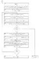
駆動ユニットは、それぞれ、アドレス情報を受信し、かつ状態情報を提供するための入力接続および出力接続を含み、駆動ユニットの出力接続が、1つの異なる駆動ユニットの入力接続に接続され、第1の駆動ユニットの入力接続が、アクティブ電圧情報に接続され、複数のうちの最後の駆動ユニットの出力接続が、接続されておらず、各駆動ユニットが、マスタ制御ユニットへの直接の通信バスをさらに備え、カウンタnの最大値を駆動ユニットの数に等しく設定することを含む方法が、
カウンタnの値に対応する駆動ユニットの入力接続の状態をチェックするステップと、状態がアクティブである場合に、
マスタ制御ユニットによって、カウンタnのその対応する値における駆動ユニットに固有のアドレスを提供し、続いて、駆動ユニットによって、マスタ制御ユニットにアドレスを返送するステップと、
カウンタnの値に対する駆動ユニットのプログラムされたアドレスを検証し、エラーがある場合には、エラー処理ルーチンを開始するステップと、そうでなければ、
カウンタnのその対応する値におけるその駆動ユニットに対するプログラミングが終了したことを信号伝達するためのフラグを設定し、続いて、駆動ユニットの出力接続をアクティブ状態に切り替えるステップと、
カウンタnの値を1だけ増加させるステップと、
カウンタnがその最大値に達するまでステップを繰り返すステップと、をさらに含む。
The drive units each include an input connection and an output connection for receiving address information and providing status information, the output connection of the drive unit being connected to the input connection of one different drive unit, and The input connections of the drive units are connected to the active voltage information, the output connections of the last of the plurality are not connected, and each drive unit further comprises a direct communication bus to the master control unit , Setting the maximum value of the counter n equal to the number of drive units,
Checking the state of the input connection of the drive unit corresponding to the value of the counter n, and if the state is active,
Providing a unique address to the drive unit at the corresponding value of the counter n by the master control unit, and subsequently returning the address to the master control unit by the drive unit;
Verifying the programmed address of the drive unit for the value of the counter n and, if there is an error, starting an error handling routine;
Setting a flag to signal that programming for that drive unit at that corresponding value of counter n has been completed, and subsequently switching the output connection of the drive unit to the active state;
Increasing the value of the counter n by one;
Repeating the steps until the counter n reaches its maximum value.
本発明の実施形態の利点は、バスプロトコルが、例えば駆動ユニットのレジスタ内のレジスタにマスクを適用することにより、いくつかのLED駆動ユニットに対して1つ以上の有効なIDを含むことができることである。無視される所定の1つまたは複数のビットは、マスクによって固定される。 An advantage of embodiments of the present invention is that the bus protocol can include one or more valid IDs for some LED drive units, for example, by applying a mask to a register in the register of the drive unit. It is. The predetermined bit or bits that are ignored are fixed by the mask.
この方法は、第1のスレーブのアドレスをカウンタnに対して1の値に設定することを含むことができる。 The method may include setting the address of the first slave to a value of one for counter n.
本発明の実施形態の利点は、MCUが、各ノードへのアドレスのセットまたはリセットを必要な任意の瞬間において初期化できることである。アドレス設定の肯定応答がLED駆動ユニットによって実行され、誤ったラベル付けの危険性が低減されるということがさらなる利点がある。MCUに対する各LED駆動ユニットの物理的位置および距離とは無関係に柔軟なアドレス設定が提供されるということがさらなる利点がある。 An advantage of embodiments of the present invention is that the MCU can initialize the setting or resetting of addresses to each node at any required moment. It is a further advantage that the acknowledgment of the address setting is performed by the LED drive unit, reducing the risk of mislabeling. It is a further advantage that flexible addressing is provided independent of the physical location and distance of each LED drive unit relative to the MCU.
この方法は、照明デバイスのための複数の駆動ユニットを駆動する方法であってもよい。 The method may be a method of driving a plurality of drive units for a lighting device.
この方法は、車両の照明用途において照明デバイス用の複数の駆動ユニットを駆動するための方法であってもよい。 The method may be a method for driving a plurality of drive units for a lighting device in a vehicle lighting application.
本発明はまた、各々が少なくとも1つの電子ユニットを駆動するための複数の駆動ユニットと、マスタ制御ユニットと複数の駆動ユニットの各々との間でデータシーケンスの交換を確立するための単一の通信バスを備えるマスタ制御ユニットと、を備えるシステムであって、各駆動ユニットが、同じ通信バスに並列に接続されており、駆動ユニットが、コントローラを備え、コントローラが、
通信バスを通じて交換されたデータを処理するための少なくとも1つのバスプロトコル処理ユニットと、
マスタ制御ユニットによって送信された任意のデータシーケンスに従って、電子ユニットの給電を制御するための少なくとも1つの制御ユニットと、をさらに備え、
少なくとも1つのバスプロトコル処理ユニット(33)が、
マスタ制御ユニットと少なくとも1つのアドレス指定された駆動ユニットとの間でデータを交換するために、少なくとも1つの駆動ユニットをアドレス指定するためのIDフィールドと、
電子ユニットの状態に関する情報および/または命令を含むデータフィールドと、を処理するように適合されており、
IDフィールドが、
Nビットを含む第1のビット部分列を使用する駆動ユニットアドレスであって、アドレス指定された駆動ユニットにデータフィールドを適用するか、または駆動ユニットがアドレス指定されていない場合には、データフィールドを無視するために、2Nが複数の駆動ユニットにおける駆動ユニットの数と等しいかまたはそれよりも多い、駆動ユニットアドレスと、
受信/送信コマンドビットであって、データが受信もしくは送信されるべきかをマスタ制御ユニットが識別することを可能にするか、または、受信/送信コマンドビットの値に依存して、どのアクションがマスタ制御ユニットによって要求されるかを各アドレス指定された駆動ユニットが解読することを可能にするための、受信/送信コマンドビットと、
データフレームに含まれる命令のタイプに関する情報を含めるための、IDフィールドにおけるさらなる機能ビットと、
さらなる機能ビットに割り当てられた値に依存して、データビットを異なる電子ユニットに割り当てるか、またはデータフィールド内のビット列の長さを示すための第2のビット部分列と、をさらに含むことを特徴とする。
The present invention also provides a plurality of drive units, each for driving at least one electronic unit, and a single communication for establishing an exchange of data sequences between the master control unit and each of the plurality of drive units. A master control unit comprising a bus, wherein each drive unit is connected in parallel to the same communication bus, the drive unit comprises a controller, and the controller comprises:
At least one bus protocol processing unit for processing data exchanged over the communication bus;
At least one control unit for controlling the power supply of the electronic unit according to any data sequence transmitted by the master control unit,
At least one bus protocol processing unit (33)
An ID field for addressing at least one drive unit for exchanging data between the master control unit and at least one addressed drive unit;
A data field containing information and / or instructions relating to the status of the electronic unit; and
ID field is
A drive unit address using a first bit sub-sequence containing N bits, either applying the data field to the addressed drive unit or, if the drive unit is not addressed, the data field A drive unit address, where 2 N is equal to or greater than the number of drive units in the plurality of drive units, to ignore;
Receive / transmit command bits, which allow the master control unit to identify whether data is to be received or transmitted, or which action, depending on the value of the receive / transmit command bits, Receive / transmit command bits to enable each addressed drive unit to decode what is required by the control unit;
An additional function bit in the ID field to include information about the type of instruction included in the data frame;
A second bit subsequence for assigning the data bits to different electronic units or indicating the length of the bit sequence in the data field, depending on the value assigned to the further function bit. And
コントローラは、マスタ制御ユニットから受信した任意のデータシーケンスの長さをチェックするためのタイミングユニットと、データの交換が所定の最小時間間隔未満で、または所定の最大時間間隔を超えて実行される場合に、エラー信号を生成する手段と、をさらに備える。 The controller has a timing unit to check the length of any data sequence received from the master control unit, and if data exchange is performed less than a predetermined minimum time interval or beyond a predetermined maximum time interval Means for generating an error signal.
一実施形態において、RC発振器は、時間軸、すなわちクロックを単に送出する。タイミングユニットは、クロックを時間軸として使用し、所与のイベント間の時間を測定し、イベント間の予測されたタイミングが保持されない場合、信号情報で作用するタイマであってもよい。 In one embodiment, the RC oscillator simply sends out a time axis, ie, a clock. The timing unit may be a timer that uses the clock as a time axis, measures the time between given events, and acts on signal information if the predicted timing between events is not preserved.
一実施形態において、タイミングユニット自体がスタンドアローンプログラマブルRC発振器を含むことができる。 In one embodiment, the timing unit itself can include a standalone programmable RC oscillator.
一実施形態において、タイミングユニット自体はスタンドアローンプログラマブルRC発振器である。 In one embodiment, the timing unit itself is a stand-alone programmable RC oscillator.
本発明の実施形態の利点は、コントローラ自体がリアルタイムエラー識別子および査定を提供することである。本発明の実施形態のさらなる利点は、エラー査定がコントローラに統合され、干渉の危険が低減されることである。 An advantage of embodiments of the present invention is that the controller itself provides the real-time error identifier and assessment. A further advantage of embodiments of the present invention is that error assessment is integrated into the controller, reducing the risk of interference.
マスタ制御ユニットは、複数の駆動ユニットのうちの少なくとも1つの駆動ユニットに給電するための共通電圧供給線をさらに備え、システムは、供給線上の少なくとも静電放電を抑制するために、少なくとも1つの駆動ユニットと共通電圧電源との間に、少なくとも1つの保護ユニットをさらに備える。 The master control unit further comprises a common voltage supply line for powering at least one of the plurality of drive units, and the system includes at least one drive line for suppressing at least electrostatic discharge on the supply line. At least one protection unit is further provided between the unit and the common voltage power supply.
本発明の実施形態の利点は、駆動ユニットが電源からの電気サージまたは電圧ピークから遮蔽されることである。 An advantage of embodiments of the present invention is that the drive unit is shielded from electrical surges or voltage peaks from the power supply.
マスタ制御ユニットの単一の通信バスは、差動通信バスであってもよい。本発明の実施形態の利点は、通信バスが外部電磁場およびアンテナ効果に対して堅固であることである。 The single communication bus of the master control unit may be a differential communication bus. An advantage of embodiments of the present invention is that the communication bus is robust against external electromagnetic fields and antenna effects.
システムは、コントローラからの電圧値を測定および収集するための診断ユニットをさらに備えていてもよい。 The system may further comprise a diagnostic unit for measuring and collecting voltage values from the controller.
本発明の実施形態の利点は、接続の寄生抵抗に起因する電圧の変動を診断し、較正することができることである。 An advantage of embodiments of the present invention is that voltage variations due to parasitic resistance of the connection can be diagnosed and calibrated.
診断ユニットは、温度センサを備えることができる。 The diagnostic unit can include a temperature sensor.
本発明の実施形態の利点は、温度変化によるLED駆動ユニットのレベルでのデータ送信および/または電圧供給の変動を較正できることである。 An advantage of embodiments of the present invention is that variations in data transmission and / or voltage supply at the LED drive unit level due to temperature changes can be calibrated.
ドライバは、診断ユニットによって与えられた任意のエラー結果に対する応答として、エラー処理ルーチンをトリガするための処理ユニットを備えることができる。 The driver may include a processing unit for triggering an error handling routine in response to any error results provided by the diagnostic unit.
本発明の実施形態の利点は、エラー信号をトリガするために診断ユニットからMCUに信号を送信するのではなく、コントローラからエラー通知を直接行うことができることである。 It is an advantage of embodiments of the present invention that instead of sending a signal from the diagnostic unit to the MCU to trigger an error signal, an error notification can be made directly from the controller.
タイミングユニットはRC発振器であってもよい。 The timing unit may be an RC oscillator.
コスト効率のよい方式で実装できるということがさらなる利点がある。 A further advantage is that it can be implemented in a cost-effective manner.
このシステムは、車両における照明用途であってもよい。 The system may be for lighting applications in vehicles.
電子ユニットはLEDであってもよい。 The electronic unit may be an LED.
本発明はまた、ビットシーケンスを含むデータフレームを、マスタ制御ユニットと、スレーブノードにおける複数の駆動ユニットのうちの少なくとも1つとの間で交換するためのバスプロトコルであって、シーケンスが、連続するビット列のフィールドの中で分割されており、シーケンスが、
マスタ制御ユニットと、少なくとも1つのアドレス指定された駆動ユニットとの間でデータを交換するために、少なくとも1つの駆動ユニットをアドレス指定するためのIDフィールドと、
電子ユニットの状態に関する情報および/または命令を含むデータフィールドと、を含み、
IDフィールドが、
Nビットを含む第1のビット部分列を使用する駆動ユニットアドレスであって、アドレス指定された駆動ユニットにデータフィールドを適用するか、または駆動ユニットがアドレス指定されていない場合にはデータフィールドを無視するために、2Nが複数の駆動ユニットにおける駆動ユニットの数と等しいかまたはそれよりも多い、アドレスと、
データが駆動ユニットから受信されるべきか、もしくは駆動ユニットに送信されるべきかを、マスタ制御ユニットが識別することを可能にするか、または、受信/送信コマンドビットに割り当てられた値に依存して、どのアクションがマスタ制御ユニットによって要求されるかを各アドレス指定された駆動ユニットが解読することを可能にするための、受信/送信コマンドビットと、
データフレームに含まれる命令のタイプに関するIDフィールドにおける情報を含むさらなる機能ビットと、
さらなる機能ビットに割り当てられた値に依存して、データビットを異なる電子ユニットに割り当てるか、またはデータフィールド内のビット列の長さを示すための第2のビット部分列と、をさらに含む。
The present invention also relates to a bus protocol for exchanging a data frame comprising a bit sequence between a master control unit and at least one of a plurality of drive units in a slave node, wherein the sequence comprises a continuous bit sequence. Are split in the field of
An ID field for addressing at least one drive unit for exchanging data between the master control unit and at least one addressed drive unit;
A data field containing information and / or instructions relating to the status of the electronic unit;
ID field is
A drive unit address using a first bit subsequence containing N bits, either applying the data field to the addressed drive unit or ignoring the data field if the drive unit is not addressed Address, where 2 N is equal to or greater than the number of drive units in the plurality of drive units;
Allows the master control unit to identify whether data is to be received from or transmitted to the drive unit, or depends on the value assigned to the receive / transmit command bits Receive / transmit command bits to allow each addressed drive unit to decode which action is required by the master control unit;
Further function bits including information in the ID field regarding the type of instruction included in the data frame;
A second bit subsequence for assigning the data bits to different electronic units or indicating the length of the bit sequence in the data field, depending on the value assigned to the further function bit.
本発明の特定の好ましい態様は、添付の独立請求項および従属請求項に記載されている。従属請求項の特徴は、適宜、独立請求項の特徴および他の従属請求項の特徴と組み合わせることができ、単に請求項に明示的に記載されたものだけではない。 Particular preferred aspects of the invention are set out in the accompanying independent and dependent claims. Features of the dependent claims may be combined with features of the independent claims and with features of other dependent claims as appropriate, and not merely as explicitly set out in the claims.
本発明のこれらおよび他の態様は、以下に記載される実施形態を参照して明らかになるであろう。 These and other aspects of the invention will be apparent with reference to the embodiments described below.
図面は概略的なものに過ぎず、限定的ではない。図面において、要素のいくつかの大きさは、説明のために誇張されており、縮尺通りに描かれていない場合がある。 The drawings are only schematic and are non-limiting. In the drawings, the size of some of the elements may be exaggerated and not drawn on scale for illustrative purposes.
特許請求の範囲内のいかなる参照符号も、範囲を限定するものとして解釈されるべきではない。 Any reference signs in the claims shall not be construed as limiting the scope.
異なる図面において、同じ参照符号は、同じまたは類似の要素を指す。 In the different drawings, the same reference signs refer to the same or analogous elements.
本発明は、特定の実施形態に関して、および、ある一定の図面を参照して説明されるが、本発明はそれに限定されず、請求項によってのみ限定される。記載された図面は概略的なものに過ぎず、限定的ではない。図面において、要素のいくつかの大きさは、説明目的のために誇張されており、縮尺通りに描かれていない場合がある。寸法および相対的な寸法は、本発明の実施に対する実際の縮小に対応していない。 The present invention will be described with respect to particular embodiments and with reference to certain drawings but the invention is not limited thereto but only by the claims. The drawings described are only schematic and are non-limiting. In the drawings, the size of some of the elements may be exaggerated and not drawn on scale for illustrative purposes. The dimensions and the relative dimensions do not correspond to actual reductions to practice of the invention.
さらに、明細書および特許請求の範囲における第1、第2などの用語は、類似の要素を区別するために使用され、必ずしも時間的に、空間的に、ランク付けまたは任意の他の方法でシーケンスを記載するために使用されるものではない。そのように使用される用語は、適切な状況下で交換可能であり、本明細書に記載された本発明の実施形態は、本明細書に記載または図示されている以外の順序で動作可能であることを理解されたい。 Furthermore, the terms first, second and the like in the description and in the claims, are used for distinguishing between similar elements, not necessarily temporally, spatially, ranked or sequenced in any other way. It is not used to describe The terms so used are interchangeable under appropriate circumstances, and the embodiments of the invention described herein are operable in an order other than that described or illustrated herein. Please understand that there is.
さらに、明細書および特許請求の範囲における用語、上、下などは、説明目的で使用され、必ずしも相対的な位置を記載するためではない。そのように使用される用語は、適切な状況下で交換可能であり、本明細書に記載される本発明の実施形態は、本明細書に記載または図示された以外の考え方で動作することができることを理解されたい。 Furthermore, the terms, above, below, etc. in the specification and claims are used for descriptive purposes and not necessarily for describing relative positions. The terms so used are interchangeable under appropriate circumstances, and embodiments of the invention described herein may operate in concepts other than those described or illustrated herein. Please understand what you can do.
特許請求の範囲で使用される用語「含む(comprising)」は、その後に列挙される手段に限定されるものとして解釈されるべきではなく、他の構成要素またはステップを排除するものではないことに留意されたい。したがって、それは、記述された特徴、整数、ステップまたは構成要素の存在を指定するものとして解釈されるが、1つ以上の他の特徴、整数、ステップまたは構成要素、またはそれらのグループの存在または追加を排除するものではない。したがって、「手段AおよびBを含むデバイス」という表現の範囲は、成分AおよびBのみからなるデバイスに限定されるべきではない。それは、本発明に関して、デバイスの最適の関連する構成要素は、AおよびBであることを意味する。 It is to be noticed that the term "comprising", used in the claims, should not be interpreted as being restricted to the means listed thereafter; it does not exclude other elements or steps. Please note. Thus, it is to be construed as specifying the presence of the recited feature, integer, step or component, but the presence or addition of one or more other features, integers, steps or components, or groups thereof. Does not exclude. Therefore, the scope of the expression "device comprising means A and B" should not be limited to devices consisting only of components A and B. That means that, in the context of the present invention, the optimal relevant components of the device are A and B.
本明細書を通じて、「一実施形態」または「実施形態」への言及は、実施形態に関連して説明される特定の特徴、構造または特性が本発明の少なくとも1つの実施形態に含まれることを意味する。したがって、本明細書を通じて様々な箇所における「一実施形態において」または「実施形態において」というフレーズの出現は、必ずしも全てが同じ実施形態を指しているわけではないが、そうであってもよい。さらに、特定の特徴、構造または特性は、1つ以上の実施形態において、本開示から当業者に明らかであるように、任意の好適な方法で組み合わせることができる。 Throughout this specification, references to "one embodiment" or "an embodiment" mean that a particular feature, structure, or characteristic described in connection with the embodiment is included in at least one embodiment of the invention. means. Thus, appearances of the phrases "in one embodiment" or "in an embodiment" in various places throughout this specification are not necessarily all referring to the same embodiment, but may. Furthermore, the particular features, structures, or characteristics may be combined in any suitable manner in one or more embodiments, as will be apparent to one skilled in the art from this disclosure.
同様に、本発明の例示的な実施形態の説明において、本発明の様々な特徴は、本開示を合理化し、かつ様々な発明的態様のうちの1つ以上の理解を助ける目的で、単一の実施形態、図、またはその説明で一緒に集められることがあることが理解されるべきである。しかしながら、この開示の方法は、クレームされた発明が、各クレームに明示的に記載されているより多くの特徴を必要とするという意図を反映するものと解釈されるべきではない。むしろ、以下の特許請求の範囲が反映するように、本発明の態様は、単一の前述の開示された実施形態の全ての特徴よりも少ないものである。したがって、詳細な説明に続く請求項は、この詳細な説明に明示的に組み込まれ、各請求項は、本発明の別個の実施形態として独立している。 Similarly, in describing exemplary embodiments of the present invention, various features of the present invention may be combined into a single unit in order to streamline the disclosure and to assist in understanding one or more of the various inventive aspects. It should be understood that they may be collected together in embodiments, figures, or descriptions thereof. However, the method of this disclosure should not be construed as reflecting an intention that the claimed invention requires more features than are expressly recited in each claim. Rather, as the following claims reflect, inventive aspects lie in less than all features of a single foregoing disclosed embodiment. Thus, the claims following the detailed description are hereby expressly incorporated into this detailed description, with each claim standing on its own as a separate embodiment of this invention.
さらに、本明細書で説明されるいくつかの実施形態は、他の実施形態に含まれる他の特徴でないものを除く、いくつかを含むが、当業者に理解されるように、異なる実施形態の特徴の組み合わせは、本発明の範囲内であり、異なる実施形態を形成することを意味する。例えば、以下の特許請求の範囲において、特許請求された実施形態のいずれかは、任意の組み合わせで使用することができる。 Furthermore, some of the embodiments described herein include some, except for other features not included in other embodiments, but as will be appreciated by those skilled in the art, Combinations of features are within the scope of the invention and are meant to form different embodiments. For example, in the following claims, any of the claimed embodiments can be used in any combination.
本明細書で提供される説明において、多くの具体的な詳細が述べられている。しかしながら、本発明の実施形態は、これらの具体的な詳細なしに実施され得ることが理解される。他の例においては、周知の方法、構造および技術は、この説明の理解を不明瞭にしないために詳細には示されていない。 In the description provided herein, numerous specific details are set forth. However, it is understood that embodiments of the invention may be practiced without these specific details. In other instances, well-known methods, structures and techniques have not been shown in detail in order not to obscure an understanding of this description.
説明において、方法およびシステムは、LEDを参照することによって例証される。それにもかかわらず、本発明の実施形態は、他のタイプの照明デバイスなどの他のタイプの電子デバイスの駆動にも等しく適用される。 In the description, the methods and systems are illustrated by reference to an LED. Nevertheless, embodiments of the present invention apply equally to driving other types of electronic devices, such as other types of lighting devices.
本発明の実施形態が「PWM」に言及される場合、パルス幅変調が参照される。しかしながら、本発明の枠組みにおいて、パルス密度変調、パルス周波数変調などの他のパルス変調技術を、LEDを制御するために使用することができる。 When embodiments of the present invention refer to "PWM", reference is made to pulse width modulation. However, in the framework of the present invention, other pulse modulation techniques, such as pulse density modulation, pulse frequency modulation, can be used to control the LED.
本発明の実施形態が「スレーブノード」に言及される場合、マスタ制御ユニット(MCU)に接続されるそれらの駆動ユニット(例えば、LED駆動ユニット)が参照される。駆動ユニットは、LEDクラスタなどの1つ以上の電子デバイスクラスタと、電子デバイスクラスタの給電を制御するコントローラとを備えることができる。 When embodiments of the present invention are referred to as “slave nodes,” those drive units (eg, LED drive units) that are connected to a master control unit (MCU) are referenced. The drive unit can include one or more electronic device clusters, such as LED clusters, and a controller that controls powering of the electronic device clusters.
第1の態様において、本発明は、各々が少なくとも1つの電子ユニットを駆動するための複数の駆動ユニットと、マスタ制御ユニットと複数の駆動ユニットの各々との間でデータシーケンスの交換を確立するための単一の通信バスを備えるマスタ制御ユニットと、を備え、各駆動ユニットが、同じ通信バスに並列に接続されているシステムに関する。このシステムは、例えば、車両もしくは自動車に対する照明システムであってもよいが、本発明の実施形態はそれに限定されない。このシステムは、電子ユニットの正確な駆動によって安全性を高めて有利である。駆動ユニットは、複数のクラスタを制御するコントローラを含む。コントローラは、通信バスを通じて交換されたデータを処理する少なくとも1つのバス処理ユニット、すなわち、マスタ制御ユニットによって送信された任意のデータシーケンスに従ってクラスタの電子ユニットの給電を制御する少なくとも1つの制御ユニットを備える。少なくとも1つのバス処理ユニットは、少なくとも1つの駆動ユニットをアドレス指定するためのIDフィールドを処理し、かつマスタ制御ユニットと少なくとも1つのアドレス指定された駆動ユニットとの間でデータを交換するように適合され、データフィールドは電子ユニットの状態に関する情報および/または命令を含んでいる。したがって、IDフィールドは、Nビットを含む第1のビット部分列を使用する駆動ユニットアドレスであって、アドレス指定された駆動ユニットにデータフィールドを適用するか、または駆動ユニットがアドレス指定されていない場合にはデータフィールドを無視するために、2Nが複数の駆動ユニットにおける駆動ユニットの数と等しいかまたはそれよりも多い、アドレスと、R/Tコマンドビットを使用して、データが受信されるべきか送信されるべきか、または各アドレス指定された駆動ユニットが、マスタ制御ユニットによってどのアクションが要求されるかを解読することを可能にする識別、データフレームに含まれる命令のタイプに関するIDフィールドにおける情報、およびビット部分列を使用して、異なる電子ユニットに割り当てられた、またはデータフィールド内のビットストリングの長さを示す、データビットを含む。このシステムは、異なるアドレスを駆動ユニットに割り当てるための柔軟な構成可能な自動アドレス指定システムを有するように適合されている。いくつかの実施形態において、このシステムは、通常、データ交換の1つ以上の段階で、例えばアドレス指定のレベルで、MCUとの間の給電または情報送信のレベルで、またはデータ交換の開始または終了のレベルでさえも、チェックポイントを提供するためのいくつかのレジスタを備えていてもよい。通常、チェックポイントは、ビットの特定の列の長さを、データ送信の特定の段階における列の予想される長さと比較することに基づいている。例えば、通信バスが突然電圧を下げるが、これが12ビット未満の長さで起こる場合、このシステムはこの事象をノイズとして無視することがある。これが12ビットの長さで起こる場合、駆動ユニットはデータシーケンスの読み取りを開始することができる。これは、送信の終了を含むデータ送信のいくつかの段階に適用することができる。これは、電磁干渉、サージ、静電気放電、および自動車環境で起こる他の望ましくない現象に対する非常に堅固な遮蔽を提供し、その結果、例えばLEDのような電子ユニットの非常に安定した堅固な駆動をもたらす。 In a first aspect, the invention provides a plurality of drive units, each for driving at least one electronic unit, and an exchange of data sequences between a master control unit and each of the plurality of drive units. And a master control unit with a single communication bus, wherein each drive unit is connected in parallel to the same communication bus. This system may be, for example, a lighting system for a vehicle or an automobile, but embodiments of the present invention are not limited thereto. This system has the advantage of increasing the safety by the precise actuation of the electronic unit. The drive unit includes a controller that controls the plurality of clusters. The controller comprises at least one bus processing unit for processing data exchanged over the communication bus, ie at least one control unit for controlling the power supply of the electronic units of the cluster according to any data sequence transmitted by the master control unit. . The at least one bus processing unit processes an ID field for addressing the at least one drive unit and is adapted to exchange data between the master control unit and the at least one addressed drive unit. The data field contains information and / or instructions regarding the status of the electronic unit. Thus, the ID field is a drive unit address using the first bit sub-sequence containing N bits, either applying the data field to the addressed drive unit, or if the drive unit is not addressed In order to ignore the data field, data should be received using an address and R / T command bits where 2 N is equal to or greater than the number of drive units in the plurality of drive units. In the ID field relating to the type of instruction contained in the data frame, which is to be transmitted or which allows each addressed drive unit to decode which action is required by the master control unit Information, and bit subsequences to different electronic units Contains data bits indicating the length of the bit string assigned or in the data field. The system is adapted to have a flexible and configurable automatic addressing system for assigning different addresses to drive units. In some embodiments, the system is typically used at one or more stages of data exchange, for example, at the level of addressing, at the level of power or information transmission to or from the MCU, or at the beginning or end of data exchange. Even at this level, several registers may be provided to provide checkpoints. Typically, checkpoints are based on comparing the length of a particular column of bits to the expected length of the column at a particular stage of data transmission. For example, if the communication bus suddenly drops the voltage, but this occurs less than 12 bits in length, the system may ignore this event as noise. If this happens with a length of 12 bits, the drive unit can start reading the data sequence. This can be applied to several stages of data transmission, including termination of transmission. This provides a very robust shield against electromagnetic interference, surges, electrostatic discharges and other undesirable phenomena that occur in the automotive environment, resulting in a very stable and robust drive of electronic units such as LEDs, for example. Bring.
本発明の実施形態において、単一ワイヤバスではなく、(例えば、2本のワイヤを有する)差動バスを使用することができる。それは、データ送信に低電圧を使用することが可能であり、比較的高価なローカル相互接続ネットワーク(Local Interconnect Network、LIN)構成の使用を避けることができるという利点がある。 In embodiments of the present invention, instead of a single wire bus, a differential bus (e.g., having two wires) may be used. It has the advantage that low voltages can be used for data transmission and the use of relatively expensive Local Interconnect Network (LIN) configurations can be avoided.
そのバスは双方向であり、光情報および診断情報を交換することが可能である。 The bus is bidirectional and can exchange optical and diagnostic information.
いくつかの実施形態においては、LINを必要とせずに60個までのスレーブノードをアドレス指定することができる。 In some embodiments, up to 60 slave nodes can be addressed without requiring a LIN.
いくつかの実施形態においては、データ送信速度が高速(750キロボー、10ms更新サイクル)に達することがある。高速に言及する場合は、LINバスで得られる速度に匹敵する速度またはそれ以上の速度が参照される。到達可能な速度は、CAN物理層の範囲内で2Mビットまでであり得る。使用される速度は、転送されるデータの量および到達すべき更新速度に依存し得る。目標となる速度は、必要な全てのデータを転送できる最小速度である。これらの高速度は、バスの並列レイアウトのおかげで得られる。例えば、ノードは、好ましくは、バスを介してMCUに並列に接続される。通信は安価でコンパクトな発振器に基づいているため、UARTが開始ビットと停止ビットを使用して全てのバイトで再同期するときの精度要件が低くなる。利点は、CANにおいて、またはSPIバスを用いて本発明を実装する必要がないので、大量のドライバ、例えばLEDドライバをスレーブノードとして安価な方法で実装できることである。 In some embodiments, the data transmission rate may reach a high rate (750 kBaud, 10 ms update cycle). When referring to high speed, a speed comparable to or higher than that available on the LIN bus is referred to. Reachable speeds can be up to 2 Mbits within the CAN physical layer. The rate used may depend on the amount of data transferred and the update rate to be reached. The target speed is the minimum speed at which all necessary data can be transferred. These high speeds are obtained thanks to the parallel layout of the bus. For example, the nodes are preferably connected in parallel to the MCU via a bus. Since the communication is based on an inexpensive and compact oscillator, the accuracy requirements when the UART uses the start and stop bits to resynchronize every byte are low. An advantage is that a large number of drivers, for example LED drivers, can be implemented as slave nodes in an inexpensive way, since there is no need to implement the invention in a CAN or with a SPI bus.
本発明は、バスプロトコルおよび/またはノード内のハードウェアレベル(機能安全レベルB)で安全機能および診断要素を提供するという条件で、システムレベルでの機能安全を提供する。本発明は、供給線上の電圧降下に対して堅固にすることができる。本発明は、例えば静電気放電(ESD)などの自動車環境における保護手段および安全対策を有利に提示して、かつ電磁適合性を改善することができる。 The present invention provides functional security at the system level, provided that it provides safety functions and diagnostic elements at the hardware level (functional safety level B) within the bus protocol and / or nodes. The invention can be made robust against voltage drops on the supply lines. The present invention can advantageously present protection measures and safety measures in an automotive environment, such as, for example, electrostatic discharge (ESD), and improve electromagnetic compatibility.
特に、本発明は、例えば、周辺光ならびにドライバのための信号情報に対する、自動車環境における動的照明システムに使用することができる。したがって、このシステムは、機能安全要件を含むことができる。本発明の実施形態は、バス実装HWおよびプロトコルにおける安全対策を含むことができる。 In particular, the invention can be used for dynamic lighting systems in an automotive environment, for example for ambient light as well as signal information for drivers. Thus, the system can include functional safety requirements. Embodiments of the present invention may include security measures in the bus implementation HW and protocols.
本発明は、調光のための専用コマンド言語、専用ハードウェア(HW)メモリおよびレジスタ手法を提供することができる。加えて、オープンな構成手段をプロトコルおよびHWに適用することができる。 The present invention can provide a dedicated command language for dimming, a dedicated hardware (HW) memory and register approach. In addition, open configuration means can be applied to protocols and HWs.
ノードは、バスノードアドレスの自動設定によって、および/またはネットワークを通じて各ノードの較正手段を実装することによって、較正することができる。自動設定はいつでも繰り返すことができる。 The nodes can be calibrated by automatic setting of the bus node address and / or by implementing a calibration means for each node over the network. Automatic configuration can be repeated at any time.
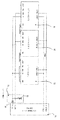
LEDに基づく例示的なシステムを示す、図1を参照して、標準的な特徴およびオプションの特徴をさらに例証する。図1は、マスタ制御ユニット(MCU)10と、MCUのスレーブノードであり、バスによってそれらの間、およびMCUに相互接続される、いくつかのLED駆動ユニット11とを備える動的照明システムを示す。さらに、駆動ユニットの電源に、1つ以上の保護ユニット12が接続されてもよい。保護ユニットは、サージまたは逆極性などに対して保護することができる。いくつかの実施形態において、1つまたは複数の保護ユニットは、電圧保護要素13、逆極性保護要素14、またはそれらの組み合わせを含むことができる。これらの保護ユニットは、供給線上の高電圧またはESD妨害を抑制し、供給線VSおよびGNDの逆極性が印加された場合のシステムの損傷を回避することができる。1つまたは複数の保護ユニットは、電源と少なくとも1つのLED駆動ユニットとの間、または複数のユニットからのユニットのうちのいくつかの間に接続されてもよい。例えば、それは、図1に示すように、電源と全てのLED駆動ユニットとの間に接続されてもよい。
Referring to FIG. 1, which illustrates an exemplary system based on LEDs, standard and optional features are further illustrated. FIG. 1 shows a dynamic lighting system comprising a master control unit (MCU) 10 and several
光情報、例えば光度、光色またはそれに関連するPWM比は、マスタ制御ユニット10からバスを介してLEDユニット11に伝達されてもよい。本発明は、LEDユニットとMCUとの間、またバスを介して、交換され得る光情報および診断情報に限定されない。診断情報は、全てのLEDが所与の電流を伝えるかどうかに関する情報を含むことができる。さらに、バスは、MCUから全てのスレーブノードへのアドレス割り当て方法もサポートすることができる。そのような場合、バス内の通信は双方向である。
Light information, such as luminosity, light color or related PWM ratio, may be transmitted from the
このシステムは、MCUのスレーブノードとしての多数のLED駆動ユニット、例えば60個のスレーブノードを含むことができる。このシステムは、例えば全てのLEDについて10msの更新サイクルでLEDを駆動して、非常に速くかつ滑らかな方式でイルミネーションに関する情報を更新するために、情報送信の高速を可能にする、例えば、(ビット形式で)パルスを送信するために750キロボーを可能にする。当該技術分野で知られているように、LINバスに基づくシステム、またはスレーブノード間で相互接続されたシフトレジスタに基づく解決策は遅すぎる。さらに、LINバスに基づくシステムでは、16個のスレーブノードしか使用できない。 The system may include a number of LED drive units as slave nodes of the MCU, for example, 60 slave nodes. This system allows for a high speed of information transmission, for example to drive LEDs with a 10 ms update cycle for all LEDs and to update information about the illumination in a very fast and smooth manner, e.g. (bit Enables (in form) 750 kilobaud to transmit the pulse. As is known in the art, systems based on LIN buses or solutions based on shift registers interconnected between slave nodes are too slow. Furthermore, in systems based on the LIN bus, only 16 slave nodes can be used.
通信バスは、いかなる種類のものであってもよいが、2つのワイヤ(例えば、COM_P、COM_N)を有する差動バスが好ましい実装である。このようなバスは、特に本発明の実施形態を含む自動車用途において、必要な通信速度、ならびに多数のスレーブノードとの通信を提供することができる。 The communication bus may be of any kind, but a differential bus having two wires (eg, COM_P, COM_N) is a preferred implementation. Such a bus can provide the required communication speed, as well as communication with a large number of slave nodes, especially in automotive applications involving embodiments of the present invention.
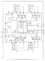
図2は、本発明の第1の態様のイルミネーションシステムに好適なLED駆動ユニット11を示す。それは、LEDコントローラ20と、1つ以上のクラスタ38に分散された1つ以上のLED37とを備える。クラスタは、例えば、LEDコントローラ20の3つのピンに接続された赤色LED、緑色LEDおよび青色LEDを含むRGBユニットであってもよい。LED駆動ユニットは、ノードアドレス指定(以下に説明するように自動アドレス指定)を可能にするために、グランド(GND)および電源(VS)への接続、ならびに通常はAINおよびAOUT接続をさらに含む。さらに、差動バスへの接続(COM_P、COM_N)が、LED駆動ユニットおよびコントローラに含まれる。本発明の実施形態において、MCUとの通信は、転送されたデータから導かれるクロックに基づくことができる。例えば、コントローラ20は、発振器41を備えることができる。
FIG. 2 shows an
MCU10の通信インターフェース(図示せず)は、スレーブノードとして作用するそれぞれのLEDユニットのコントローラ20の通信インターフェース32、33、34と共に、差動の双方向バスを形成することができる。光情報、較正データ、診断情報、および他のタイプのデータをこのバスを通じて伝達することができる。
The communication interface (not shown) of the
LEDユニットコントローラ20は、集積回路(IC)内に含まれてもよい。コンパクトなコントローラを有利に設けることができる。これは、例えば、1つ以上のスイッチ要素制御21を含むことができる。これらを使用し、1つ以上のスイッチ要素40を介して、1つ以上の外部消費者に電源電圧を提供することができる。スイッチ要素40は、例えばトランジスタであってもよい。スイッチ要素制御は、例えば、マイクロコントローラ27によって制御される。
The
コントローラ20は、電流源、スイッチ要素、およびパルス幅変調(PWM)の制御22をさらに含むことができる。1つの制御22をクラスタごとに設けることができ、または例えば、図2bに示す多重化を介して、単一の制御22を複数のクラスタ22を制御するために設けることができる。マイクロコントローラ27は、含まれるPWMレジスタに周波数およびデューティサイクルに関する情報を提供することができる。周波数とデューティサイクルは、全てのPWMレジスタで異なる場合があり、静的なオン/オフにすることもできる。言い換えれば、ドライバは一定のオンまたは一定のオフ値に駆動することもできる。電流源39およびスイッチ要素40は、各PWMレジスタに接続することができ、PWMレジスタは、提供されたPWMまたは静的なオン/オフを含むことができる。マイクロコントローラはさらに、1つ以上の異なる電流源に対する情報および命令をさらに提供する。この情報は、例えば、接続された電流源が適用するDC電流値を含むことができる。各電流源は異なるDC電流を伝えることができる。各電流源はさらに、例えば、接続されたPWMレジスタを介して提供されるPWMで変調することができる。各スイッチ要素40および電流源39は相互接続され、クラスタ38の発光ダイオードLED37に接続されることができる。したがって、スイッチ要素40と電流源39の両方がLED37を駆動することができる。各LEDは、スイッチ要素と電流源を介して個別に制御することができ、両方ともPWMで変調することができ、またはDC電流を使用して静的に駆動することができるので、各LEDは、LEDごとに0%〜100%の範囲の光出力に到達することができる個々の光強度を伝えることができる。スイッチ要素と電流源との組み合わせにより、LEDユニットコントローラ内の電力損失の態様の下でLEDを最適に制御することが可能である。
The
しかしながら、本発明はこれに限定されるものではない。ドライバは、1つ以上の電流源およびPWM制御部23に接続された電流源39のみを代替的または追加的に備えることができる。マイクロコントローラ27は、含まれるPWMレジスタに周波数およびデューティサイクル情報を提供することができる。周波数およびデューティサイクルは、全てのPWMレジスタで異なることができ、それは静的なオン/オフでもよく、各PWMレジスタは、提供されたPWM(または静的オン/オフ)を伝えることができる電流源39を制御する。マイクロコントローラは、既に説明したように、異なる電流源情報および命令をさらに提供する。各電流源は異なるDC電流を伝えることができ、接続されたPWMレジスタを介して提供されるPWMで変調される。LEDは電流源を介して個別に制御され、次に、直流電流の使用下でPWMによってまたは静的な方式で制御されるので、各LEDは個々の光強度を伝えることができ、LEDごとに0%〜100%の光出力に達することもできる。
However, the present invention is not limited to this. The driver may alternatively or additionally comprise only one or more current sources and a
この実装は、スイッチング要素によって供給される電流源(または静的電源)における調整可能なDC電流の使用下で、LEDの線形制御を可能にする。それは、PWM駆動、または両方の組み合わせも可能である。 This implementation allows for linear control of the LED under the use of an adjustable DC current in the current source (or static power supply) provided by the switching element. It can be PWM driven, or a combination of both.
スイッチのタイプは、有利なことにトランジスタであり、電流源も有利なことに電流供給モードで制御されるトランジスタである。トランジスタと電流源はグラウンドまたは電源に関連することができる。 The type of switch is advantageously a transistor, and the current source is also advantageously a transistor controlled in a current supply mode. The transistor and current source can be associated with ground or a power supply.
LEDユニット11のコントローラ20は、外部供給電圧(例えば、カーバッテリ電源電圧VS)を調整し、それをLED駆動ユニットによって必要とされる電圧に適合させるための電圧調整器26をさらに備える。例えば、電圧調整器は、内蔵コントローラに必要な低電圧にまで電源電圧VSを調整することができる。ドライバは、例えば調整器に接続された少なくとも1つの発振器41を備えることができる。発振器は、調整可能な周波数を有する発振器であってもよく、例えば、マイクロコントローラ27、スイッチ要素用の制御ユニット22、電流源およびPWM、電流源およびPWM用の制御ユニット23、タイマ(図示せず)など、タイムベースを必要とし得るコントローラ20の全ての要素にシステムクロックを提供することができる。発振器41は、RC発振器41であってもよい。これらは、コンパクトで安価(少なくともCAN実装で通常使用される水晶発振器よりも安価)であり、コントローラのコストを有利に低減して、したがって、多数のスレーブノードを低コストでMCUに接続することができる。
The
マイクロコントローラ27は、計算を実行し、アドレスまたはデータバスを介してコントローラの接続されたユニットに情報を受信および/または提供する中央処理ユニット(CPU)28を含むことができる。CPUは、CPUによって処理されるプロセスに即時または今後影響を及ぼす可能性がある割り込み命令を受信するように適合されてもよい。マイクロコントローラは、例えば異なるPWMレジスタに対するPWM比であって、MCU10によって提供されることがあり、通常は提供される、光強度要求の応答として即座に計算される(「オンザフライ(on the fly)で」計算される)、PWM比のデータ処理のためのデータ処理中に使用することができるデータ記憶装置をさらに備えることができる。データ記憶装置29は、いくつかのデータバッファを含むランダムアクセスメモリ(RAM)であってもよい。
Microcontroller 27 may include a central processing unit (CPU) 28 that performs calculations and receives and / or provides information to connected units of the controller via an address or data bus. The CPU may be adapted to receive interrupt instructions that may have an immediate or future effect on the processes handled by the CPU. The microcontroller may be provided by the
マイクロコントローラは、データメモリ30および/またはプログラムメモリ31をさらに備えることができる。これらのメモリの本質は、電源が低下するときにデータを失わないということである。例えば、これらのメモリは、不揮発性(NV)メモリであってもよい。プログラムメモリ31は、CPUのための命令が記憶され得るNVメモリであってもよい。このようなメモリは、例えば、読み出し専用メモリ(ROM)またはフラッシュメモリとすることができる。マイクロコントローラ27は、例えば、較正データ、アドレス情報、状態情報などのデータを含むことができるEEPROMなどのデータメモリ30をさらに備えることができる。
The microcontroller can further include a
LEDコントローラが集積回路である本発明のいくつかの実施形態において、PWM制御とADC測定とを互いの間で同期させることができるので、PWMスイッチングによる測定誤差を排除することができる。しかしながら、例えば、LEDユニットコントローラの1つ以上のピンからの電圧を測定および収集するために、診断ユニット35が含まれ得る。このユニット35は、アナログデジタル変換器(ADC)を備えることができる。それは、さらに、接続されたLEDを通じて流れる電流などを測定することもできる。診断ユニット35は、集積回路の温度測定値を提供するための温度センサをさらに備えることができる。診断ユニット35は、CPUによっていつでも読み取ることができる。CPUは、測定結果のチェックを行い、それらを、例えばNVデータメモリ中にある、またはMCUを介して提供される、予測値(閾値)と比較してもよい。測定値が所与の閾値を上回るか下回っている場合、CPUは、例えば、エラー処理ルーチンのためにトリガすることができ、またはシステムが通常の動作状態に戻れるように調整プロセスを開始することができる。集積回路の温度が例えばあまりに高い(例えば、バスおよび接続の抵抗に影響し始めるのに十分に高い)場合、CPUは省電流モードに切り替え始めるか、または接続されているLEDを減光し始めることができる。指定のスレーブノードの全てのセキュリティ対策は、次に、他の対策のために他のLED駆動ユニットをトリガし得るMCUに通信されるので、システムを保護するためにシステム全体の性能が低下する可能性がある。 In some embodiments of the present invention where the LED controller is an integrated circuit, the PWM control and the ADC measurement can be synchronized between each other, so that measurement errors due to PWM switching can be eliminated. However, a diagnostic unit 35 may be included, for example, to measure and collect voltage from one or more pins of the LED unit controller. This unit 35 can include an analog-to-digital converter (ADC). It can also measure, for example, the current flowing through the connected LEDs. The diagnostic unit 35 may further comprise a temperature sensor for providing a temperature measurement of the integrated circuit. The diagnostic unit 35 can be read at any time by the CPU. The CPU may check the measurement results and compare them with predicted values (thresholds), for example, in NV data memory or provided via an MCU. If the measurement is above or below a given threshold, the CPU may trigger, for example, for an error handling routine, or may initiate an adjustment process so that the system can return to normal operating conditions. it can. If the temperature of the integrated circuit is, for example, too high (e.g., high enough to start affecting the resistance of the bus and connections), the CPU may start switching to a current saving mode or start dimming the connected LEDs. Can be. All security measures of the designated slave node are then communicated to the MCU which can trigger other LED drive units for other measures, so the overall system performance may be reduced to protect the system There is.
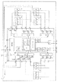
既に説明したように、信号は通信バスを介して送信される。図3は、コントローラ内の信号経路の可能な実装を示す。差動通信バスを含む本発明の実施形態において、コントローラ20は、これらの外部バス信号を、LEDユニットコントローラによって使用される内部受信(RX)および/または送信(TX)信号に変換するために、差動バス信号COM_P、COM_Nに接続される差動物理層34を備えることができる。差動物理層は、自動車用ハーネスからのESDおよびEMCの影響に対して集積回路を保護し、EMCコンプライアンス全体の対策を講じる。データは、物理層34と汎用非同期受信機送信機UART32との間で交換される。
As already explained, the signals are transmitted via the communication bus. FIG. 3 shows a possible implementation of the signal path in the controller. In embodiments of the present invention that include a differential communication bus, the
バスプロトコル処理ユニット(BPPU)33は、受信/送信されるデータの処理を実行し、機能上の安全対策を適用し、および/または必要とされる場合にエラー処理をトリガする。BPPUはまた、割り込みおよび制御信号を生成し、それらをCPUおよびUART32に送ることができる。全体的な実装により、CPUのリソースの必要性が軽減される。BPPU33は、例えば、デジタル状態機械、または動的照明用途のためのバスプロトコルを処理するための任意の他のタイプのユニットを含むことができる。
A bus protocol processing unit (BPPU) 33 performs processing of the received / transmitted data, applies functional security measures, and / or triggers error handling when needed. The BPPU can also generate interrupt and control signals and send them to the CPU and
タイマまたはタイミングユニット55を使用して、データシーケンスの長さをチェックすることができる。シーケンスの長さまたはその一部が予想値と一致しない場合、エラー信号を生成することができる。 A timer or timing unit 55 can be used to check the length of the data sequence. If the length of the sequence, or a portion thereof, does not match the expected value, an error signal can be generated.
データ記憶装置29の1つ以上のデータバッファ52、53、54への直接アクセスを提供するために、少なくとも1つのダイレクトメモリアクセスコントローラ(DMA)50、51を含めることができる。これは、UARTが、第1の受信データ記憶バッファ52または第2の受信データ記憶バッファ53に直接受信(DMA_RX)のダイレクトメモリアクセス制御を介しBPPUのデータ処理を介して、受信データを受信モードにすることができるので、MCUとの間の通信ニーズに関するCPUの負荷を最小限にするという利点をもたらす。BPPUは、例えばRX_Addressによって提供されたアドレス情報によって、どのデータ記憶バッファが使用されるかを選択する。
At least one direct memory access controller (DMA) 50, 51 may be included to provide direct access to one or more data buffers 52, 53, 54 of the data storage device 29. This is because the UART sets the reception data in the reception mode through the BPPU data processing via the direct reception (DMA_RX) direct memory access control to the first reception data storage buffer 52 or the second reception
一実施形態において、データフレームは、例えば交互にデータ記憶バッファに記憶することもでき、例えば、各第1のデータフレームは、例えば第1の受信データ記憶バッファ52に記憶され、各第2のデータフレームは、例えば第2の受信データ記憶バッファ53に記憶される。これにより、新しい各着信データフレームでのデータの上書きが回避される。
In one embodiment, the data frames may be stored in the data storage buffer, for example, alternately, for example, each first data frame may be stored in the first received data storage buffer 52, for example, and each second data frame may be stored in the first data storage buffer 52. The frame is stored, for example, in the second reception
受信モードおよび送信モードは、バスプロトコルに依存して、例えばBPPUによってCPUとUARTにトリガされ得る。送信モードにおいて、CPUは、共通アドレスおよびデータバスを介して、データを送信データ記憶バッファ54にもっていくことができる。BPPUは、例えば、TX_Addressによって提供されるアドレス情報の使用の下、送信(DMA_TX)51に対するダイレクトメモリアクセス制御の使用の下で、このデータを送信データ記憶バッファ54から受け取ることができ、そのデータをUARTに転送し、さらにBPPUはそのデータを処理する可能性がある。 The reception mode and the transmission mode can be triggered by the CPU and UART, for example, by the BPPU, depending on the bus protocol. In the transmission mode, the CPU can bring data to the transmission data storage buffer 54 via the common address and data bus. The BPPU can receive this data from the transmit data storage buffer 54 and use the data, for example, using the address information provided by the TX_Address, and using direct memory access control for the transmission (DMA_TX) 51. To the UART, and the BPPU may process the data.
データ記憶バッファは、バスプロトコルを最適な方式で処理するために、例えば、38バイトまたは40バイトの大きさを有する。いくつかのデータ記憶装置およびバッファを含めることができる。例えば、エラーレジスタをデータ記憶装置29のデータバッファとして含めることができる。 The data storage buffer has a size of, for example, 38 or 40 bytes in order to handle the bus protocol in an optimal manner. Several data storage devices and buffers can be included. For example, an error register can be included as a data buffer in the data storage device 29.
さらに、MCUと、またはコントローラの異なるユニット内で、交換されたデータシーケンスの長さをチェックするためのタイミングユニットを含めることができる。さらに、例えば、比較器70、調整可能な基準電圧71を設定するためのユニット、デバウンス(debouncing)ユニット72、異なるレジスタ73、74、ならびに他のLED駆動ユニットに接続され得る入力および出力用のピンを含む、自動アドレス指定制御および接続を含めることができる。
In addition, a timing unit for checking the length of the exchanged data sequence in the MCU or in a different unit of the controller may be included. Further, for example, a comparator 70, a unit for setting an adjustable reference voltage 71, a debounce unit 72,
LEDユニット11内のコントローラのピンへのLEDクラスタの接続は、任意の好適な方式で適合させることができる。一実施形態において、コントローラ20は、例えば図2Aで実証されたように4つのRGBユニット38を駆動することができる。この実施形態において、各LEDクラスタ38は、電源VSおよび少なくともコントローラ20の電流源に接続される。別の実施形態において、コントローラ20は、例えば、図2Bで実証されたように、6つのRGBユニットを駆動することができる。この特定の実施形態において、LEDクラスタはコントローラの異なるピンに接続され、いずれも電源に接続されていない。いくつかのクラスタは、スイッチと電流源に、またはスイッチにのみ接続されたそれらのLEDアノードを有し、一方、カソードは電流源に接続することができる。
The connection of the LED cluster to the pins of the controller in the
さらなる態様において、本発明は、電子ユニットに給電するための複数の駆動ユニットを動作させる方法にも関する。この方法は、マスタ制御ユニット(MCU)と、スレーブノードにおける複数の駆動ユニットのうちの少なくとも1つとの間で、連続するビット列のフィールドに分割されているビットシーケンスを含むデータフレームを交換することを含む。 In a further aspect, the invention also relates to a method of operating a plurality of drive units for powering an electronic unit. The method comprises exchanging a data frame between a master control unit (MCU) and at least one of a plurality of drive units in a slave node, the data frame comprising a bit sequence divided into a field of a continuous bit sequence. Including.
本方法は、マスタ制御ユニットと、少なくとも1つのアドレス指定された駆動ユニットとの間でデータを交換するために、少なくとも1つの駆動ユニットをアドレス指定するためのIDフィールドを適用することと、電子ユニットの状態に関する情報および/または命令を含むデータフィールドを適用することと、を含む。IDフィールドを適用することは、Nビットを含む第1のビット部分列を使用して駆動ユニットにアドレスを示すことであって、アドレス指定された駆動ユニットにデータフィールドを適用するか、または駆動ユニットがアドレス指定されていない場合にはデータフィールドを無視するために、2Nが複数の駆動ユニットにおける駆動ユニットの数と等しいかまたはそれよりも多い、示すことと、R/Tコマンドビットを使用して、データが受信されるべきか、もしくは送信されるべきかを、マスタ制御ユニットが識別することを可能にするか、または、どのアクションがマスタ制御ユニットによって要求されるかを各アドレス指定された駆動ユニットが解読することを可能にすることと、F機能ビットを使用して、データフレームに含まれる命令のタイプに関する情報をIDフィールドに含めるための長さ解読ステップを実行することと、データビットを異なる電子ユニットに割り当てること、または第2のビット部分列を使用してデータフィールド内のビット列の長さを示すことと、を含む。別の態様においては、本発明はまた、対応するバスプロトコルに関する。 The method includes applying an ID field for addressing at least one drive unit to exchange data between the master control unit and at least one addressed drive unit; Applying a data field containing information and / or instructions regarding the status of the Applying the ID field is to indicate an address to the drive unit using a first bit sub-sequence including N bits, either applying the data field to the addressed drive unit, or Use the R / T command bit to indicate that 2 N is equal to or greater than the number of drive units in the plurality of drive units to ignore the data field if is not addressed. The master control unit is able to identify whether data is to be received or transmitted, or to specify which action is required by the master control unit. Using the F function bit to enable the drive unit to decode Performing a length decoding step to include information about the type of instruction in the ID field, assigning the data bits to different electronic units, or using the second bit subsequence to determine the sequence of bits in the data field. Indicating the length. In another aspect, the invention also relates to a corresponding bus protocol.
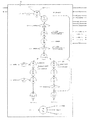
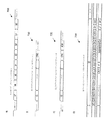
駆動ユニットを動作させるための方法およびバスプロトコルのさらなる標準およびオプションの特徴を、以下に記載するような特定の例として例証する。以下、例示的なバスプロトコルおよびアドレス指定方法を記載する。比較のために、プロトコルUARTが、図7の上の図面700に示されている。本発明の例示的な実施形態によれば、MCUと、スレーブノードとして動作する複数のLED駆動ユニットとの間でデータを交換するために、動的照明システム用のバスプロトコルが提供される。動的照明システムの開示されたバスプロトコルは、一般的にUARTプロトコルのような標準バスプロトコルに準拠していない。提案されたバスプロトコルは、列またはフィールドにグループ化された連続するビットのシーケンスを含んだデータフレームを含む。データフレームは、IDフィールドおよびデータフィールドを含む。図7の第2の図面710に示される例示的な実施形態において、動的照明システムのバスプロトコルは、例えばアクティブロー(バスが非アクティブであるときに高電圧とは対照的に低電圧)であるブレークフィールドを含む。ブレークフィールドは、データフレームの開始時に例えばアクティブローである、任意の数のビット、例えば1ビット、または例えば12ビットを含むことができる。12ビット時間の長さは、この長さがUARTの完全なデータフレーム(全体で10ビット、図7の上の図面700参照)よりも長いという利点を有する。これは、ブレークフィールドでデータフレームの開始を認識するために、自動車環境に十分なヘッドルームを残す。
Further standard and optional features of the method and bus protocol for operating the drive unit are illustrated as specific examples as described below. The following describes an exemplary bus protocol and addressing method. For comparison, the protocol UART is shown in the drawing 700 above FIG. According to an exemplary embodiment of the present invention, a bus protocol for a dynamic lighting system is provided for exchanging data between an MCU and a plurality of LED drive units operating as slave nodes. The disclosed bus protocol for dynamic lighting systems generally does not conform to a standard bus protocol such as the UART protocol. The proposed bus protocol involves a data frame containing a sequence of consecutive bits grouped into columns or fields. The data frame includes an ID field and a data field. In the exemplary embodiment shown in the
動的照明用途のためのバスプロトコルは、前述のようにIDフィールドの後に可変データ長のデータフィールドをさらに含むことができる。バイトの性質は任意のタイプであってもかまわない。 The bus protocol for dynamic lighting applications may further include a variable data length data field after the ID field as described above. The nature of the byte may be of any type.
例えば、一実施形態においては、それは例えば光情報を含むことができる。光情報は、RGBユニット内のLEDを制御するPWMレジスタのための直接情報とすることができる。それはまた、RGBユニットの光度または光色の情報だけでもある。この場合、LEDユニットコントローラのCPUは、この提供された情報を使用してPWMレジスタのPWM設定を計算することができる。 For example, in one embodiment, it can include, for example, optical information. The light information can be direct information for a PWM register that controls the LEDs in the RGB unit. It is also just the luminosity or light color information of the RGB units. In this case, the CPU of the LED unit controller can calculate the PWM setting of the PWM register using the provided information.
別の実施形態において、データは、例えば、消費者に電源を供給するための、スイッチ要素40に対する単なる情報であってもよい。 In another embodiment, the data may be merely information for the switch element 40, for example, to power a consumer.
別の実施形態において、データフィールドは、MCUに対するスレーブノードの診断情報を含むことができる。これは、例えば、照明ユニットコントローラの温度情報であってもよい。 In another embodiment, the data field may include slave node diagnostic information for the MCU. This may be, for example, temperature information of the lighting unit controller.
別の実施形態において、データは、例えば、全てのスレーブノードに対する同報コマンドであり得る。例えば、全てのスレーブノードが全てのLEDをオフに切り替えるように指示するコマンドであってもよい。1つ以上の実施形態において、他のコマンドは、また1つ以上の組み合わせで、例えば、以下のように定めることができる。
enter 例えば、アプリケーションモードに入る。
enter 例えば、例えば、定められた光出力を全てのLEDに予め設定するために較正モードに入る。
enter 例えば、さらに説明するように自動アドレッシングモードに入る。
enter 例えば、NVプログラムメモリ(31)のためのプログラミングモードに入る。
send 例えば、LEDおよび/またはLEDユニットに色情報を送る。
enable LEDの駆動モード(例えば、線形駆動またはPWM駆動)を可能にする。
request 例えば、全てのLEDが電流を伝える場合に診断を要求する。
request 例えば、スレーブアドレスを要求する。
request 例えば、LED RGBユニットのための色情報を要求する。
request 温度情報を要求する。
write 所与のメモリ位置にデータを書き込む。
read 例えば、所与のメモリ位置からデータを読み出す。
enter 例えば、スリープモードなどの動作によってスタンドに入るなど。
In another embodiment, the data may be, for example, a broadcast command for all slave nodes. For example, it may be a command that instructs all slave nodes to switch off all LEDs. In one or more embodiments, other commands may also be defined in one or more combinations, for example, as follows.
enter, for example, enter application mode.
enter, for example, enter a calibration mode to preset a defined light output to all LEDs.
enter, for example, an automatic addressing mode as described further below.
enter, for example, a programming mode for the NV program memory (31).
send For example, send color information to the LED and / or LED unit.
Enables the drive mode of the enable LED (eg, linear drive or PWM drive).
request For example, a diagnosis is requested when all LEDs transmit current.
request For example, a slave address is requested.
request For example, request color information for an LED RGB unit.
request Requests temperature information.
write Write data to a given memory location.
read For example, read data from a given memory location.
enter For example, entering the stand by operation such as sleep mode.
いくつかの他のコマンドも同様に実装することができる。データフィールドは柔軟性がある。 Some other commands can be implemented as well. Data fields are flexible.
いくつかの実施形態において、動的照明用途ためのバスプロトコルは、必要に応じて、データフィールドに続く、例えば16ビットの巡回冗長チェック(CRC)フィールドを含むことができる。CRC生成およびCRCチェックは、IDフィールドおよびデータフィールドにわたって行うことができる。CRC計算は最先端技術のCRC計算に従うので、これ以上記載しない。 In some embodiments, a bus protocol for dynamic lighting applications may optionally include a data field followed by a cyclic redundancy check (CRC) field, for example, of 16 bits. CRC generation and CRC checking can be performed over the ID and data fields. The CRC calculation follows the state-of-the-art CRC calculation and will not be described further.
データフレームの終了において、例えばCRCフィールドの後に、フレームの終了(End of Frame)が続くことがある。図7の部分700によれば、フレームの終了は、一実施形態においては、UART送信と同様に、アクティブにハイである、単なる停止ビットであり得る。フレームの終了は他の長さを表示することができる。例えば12ビット時間のように、例えば、多くのより長いビット時間を提示することもできる。
At the end of a data frame, for example, an end of frame (End of Frame) may follow the CRC field. According to
図7の第3の図面720に示される、さらなる実施形態において、CRCフィールドの後に、肯定応答(ACK)フィールドが続き、前述のように、フレームの終了フィールドが続く場合がある。肯定応答フィールドは、受信データフレームにのみ作用し、スレーブノードによって行われる。肯定応答フィールドは、CRCフィールドの直後にスレーブノードによって送られる1バイトを含むことができる。スレーブは、データの受信がOKで、エラーが発生していなかった場合は、事前に定義されたバイトを送ることがある。バイトは、例えば、01111110で事前に定義されてもよい。肯定応答情報はMCUによって知られている(例えばそこにプログラムすることができる)ので、これとは異なる受信された情報は、妨害された通信チャネルの識別につながり、MCUがこのエラーを診断し、エラー処理においてさらなる対策を講じることを可能にする。
In a further embodiment, shown in the
一実施形態において、データの受信が完全ではなく、かつ正しい場合、肯定応答フィールドは00000000である可能性がある。別の実施形態においては、データの受信が完全でないか不正確である場合、ACKは送らない可能性がある。 In one embodiment, the acknowledgment field may be 00000000 if the reception of the data is not complete and correct. In another embodiment, if the reception of the data is incomplete or incorrect, an ACK may not be sent.
全てのこのような場合、MCUはデータの受信中にエラーがあったかどうかを診断することができる。 In all such cases, the MCU can diagnose if there was an error while receiving the data.
本発明の一実施形態において、ブレークフィールドから始まる次のデータフレームは、UART送信の停止ビットの直後に続くことができる。 In one embodiment of the present invention, the next data frame starting from the break field may immediately follow the stop bit of the UART transmission.
次の段落では、本発明の実施形態においてセキュリティプロトコルおよびチェックを含む例示的なIDフィールドについて説明する。本発明の実施形態において、IDフィールドは、例えば、ブレークフィールドの後に続く複数のビットを含む。IDフィールドのうちのなくとも1ビットは、スレーブノードとして作用するLED駆動ユニットをアドレス指定するために割り当てられる。好ましくは、ビットの第1の部分列がスレーブノードアドレスに割り当てられる。さらに、IDフィールドは、データフレームが送信用または受信用のデータフィールドを含むかどうかの情報を含む、コマンドビットである少なくとも1つのさらなるビットを含む。さらに、IDフィールドは、データフレームの機能を表す機能ビットと、データフレームの指定機能に対応する値を割り当てるための少なくとも1つの、好ましくは複数のさらなるビットとを含む。例えば、データフレームがイルミネーションシステムの電源を入れるMCUからの命令を含む場合、複数のビットがLED駆動ユニット内の個々のLEDの指定アドレスに割り当てられてもよい。例えば、複数のビットは、後続のデータフィールドに存在するビットの数を表す値を含むことができる。 The following paragraphs describe exemplary ID fields that include security protocols and checks in embodiments of the present invention. In an embodiment of the present invention, the ID field includes, for example, a plurality of bits following the break field. At least one bit of the ID field is allocated to address the LED drive unit acting as a slave node. Preferably, a first substring of bits is assigned to a slave node address. Further, the ID field includes at least one additional bit, which is a command bit, including information on whether the data frame includes a data field for transmission or reception. Further, the ID field includes a function bit indicating a function of the data frame and at least one, preferably a plurality of further bits for assigning a value corresponding to the specified function of the data frame. For example, if the data frame includes a command from the MCU to power on the illumination system, multiple bits may be assigned to the designated address of each LED in the LED drive unit. For example, the plurality of bits can include a value representing the number of bits present in a subsequent data field.
図7の第4の図面730は、本発明の実施形態によるIDフィールドの例示的な実施形態を示す。例えば、動的照明用途のバスプロトコルは、ブレークフィールドに続いて16ビットIDフィールドをさらに含む。
The
IDフィールドの上位6ビット(ID15、ID14、ID13、ID12、ID11、ID10)がスレーブアドレス指定を示してもよい。これにより、64個のスレーブに対応できる。いくつかの実施形態においては、いくつかのアドレスを固定することができる。例えば、光バスプロトコルの定義において、4つの最低アドレス000000、000001、000010、000011(または4つの最高アドレス111111、111110、111101、111100、または任意の他の所定のアドレス指定またはアドレス指定のセット)が、全てのスレーブノードの有効なIDとみなすことができる。この特定の実施形態は、MCUが同報方式で全てのスレーブノードに同時にアドレス指定することができるという利点を有する。換言すれば、全てのスレーブノード(全てのLED駆動ユニット)がこれらのIDを有効なIDとして解釈する。これは、例えば、各個々のスレーブノードが、照明設定情報を受信し、この設定を記憶するだけのアプリケーションに対するインスタンス空間を残す。同報コマンドを使用すると、全てのスレーブノードが、1回かつ同時にこの照明設定を適用し、その結果、システム全体が照明設定の均等な変更を示す。6ビットのIDフィールドを有し、同報のために4つのアドレス指定を使用する特定の実施形態において、選択された実装は60個のスレーブノードをアドレス指定することを可能にする。 The upper 6 bits (ID15, ID14, ID13, ID12, ID11, ID10) of the ID field may indicate the slave address designation. Thereby, 64 slaves can be handled. In some embodiments, some addresses may be fixed. For example, in the definition of the optical bus protocol, the four lowest addresses 000000, 000001, 0000010, 000011 (or the four highest addresses 111111, 111110, 111101, 111100, or any other predetermined addressing or set of addressing). , Can be regarded as valid IDs of all slave nodes. This particular embodiment has the advantage that the MCU can address all slave nodes simultaneously in a broadcast manner. In other words, all slave nodes (all LED drive units) interpret these IDs as valid IDs. This leaves instance space for applications, for example, where each individual slave node receives the lighting setting information and only stores this setting. Using the broadcast command, all slave nodes apply this lighting setting once and simultaneously, so that the entire system shows an even change in lighting setting. In certain embodiments having a 6-bit ID field and using four addressing for broadcast, the selected implementation allows addressing 60 slave nodes.
さらに、IDフィールドのID9は、受信(R)または送信(T)コマンドビットを含む。例えば、ID9=0は受信に等しいので、データフレームはMCUからドライバに送られたデータフィールドを含み、例えば、ID9=1は送信に等しいので、データフレームはドライバからMCUに送られたデータフレームである。これにより、データを受信すべきである場合、またはデータを送信すべきである場合、マスタが各スレーブを個別方式で制御することが可能になる。さらに、スレーブノードは、どのアクションがマスタ制御ユニットによって要求されるかを解読することができる。ID9に割り当てられた値は異なり得る。 Further, ID9 in the ID field includes a receive (R) or transmit (T) command bit. For example, since ID9 = 0 is equivalent to reception, the data frame includes a data field sent from the MCU to the driver. For example, since ID9 = 1 is equivalent to transmission, the data frame is a data frame sent from the driver to the MCU. is there. This allows the master to control each slave in an individual manner when data is to be received or data is to be transmitted. Further, the slave nodes can interpret which actions are required by the master control unit. The value assigned to ID9 can be different.
IDフィールドの次のビットID8は、さらなる機能情報Fを含むことができる。 The next bit ID8 of the ID field can contain further function information F.
例えば、ID8=1の場合、受信モードの受信データは、サブアドレス(SubAddress)ID7、ID6、ID5、ID4、ID3、ID2に6バイトを乗じたビット数で定められる長さを有する。これは0バイト(ビットセットなし:ID[7:2]=000000)と、36バイト(全てのビットセット:ID[7:2]=111111)の間の可変データ長のための空間を残す。 For example, when ID8 = 1, the reception data in the reception mode has a length determined by the number of bits obtained by multiplying the sub-addresses (SubAddress) ID7, ID6, ID5, ID4, ID3, and ID2 by 6 bytes. This leaves space for a variable data length between 0 bytes (no bit set: ID [7: 2] = 000000) and 36 bytes (all bit sets: ID [7: 2] = 111111).
LED駆動ユニットのLEDクラスタには番号を付けることができるため、アドレス指定することができる。例えば、(例えば、図2Bに示されるような)LEDユニット11のRGBユニット38は、例えば、RGBユニット0、RGBユニット1、RGBユニット2、RGBユニット3、RGBユニット4、RGBユニット5として、ランダムな順序で、またはMCUによって選択された順序で番号付けられることが可能である。
Since the LED clusters of the LED drive unit can be numbered, they can be addressed. For example, the
さらに、サブアドレス[7:2]のビット位置が、番号付きRGBユニットに割り当てられてもよい。これは、例えば、次の割り当てにつながることができる。
ID7−RGBユニット5 ID7=1の場合は6データバイト、ID7=0の場合は0データバイトがRGBユニット5に割り当てられる。
ID6−RGBユニット4 ID6=1の場合は6データバイト、ID6=0の場合は0データバイトがRGBユニット4に割り当てられる。
ID5−RGBユニット3 ID5=1の場合は6データバイト、ID5=0の場合は0データバイトがRGBユニット3に割り当てられる。
ID4−RGBユニット2 ID4=1の場合は6データバイト、ID4=0の場合は0データバイトがRGBユニット2に割り当てられる。
ID3−RGBユニット1 ID3=1の場合は6データバイト、ID3=0の場合は0データバイトがRGBユニット1に割り当てられる。
ID2−RGBユニット0 ID2=1の場合は6データバイト、ID2=0の場合は0データバイトがRGBユニット0に割り当てられる。
Further, the bit positions of the sub address [7: 2] may be assigned to the numbered RGB units. This can, for example, lead to the next assignment.
ID7-
ID6-
ID5 to
ID4-
ID3-
ID2-
各RGBユニット38は、例えば3つの個々のLED37を含むことが分かる(図2A、2B)。スイッチ要素、電流源およびPWMのための制御22に含まれる1つのPWMレジスタは、例えば16ビット(2バイト)幅とすることができる。各LEDはPWMレジスタによって制御される。したがって、2バイトにRGBユニット当たり3つのLEDを乗じたものは6バイトに等しい。したがって、1つのRGBユニットの光情報設定には6バイトが必要となる。明らかに、選択された実装は、図2Bに示されるもののようなLEDユニットのための完全な光情報設定を送信することを可能にする。
It can be seen that each
一方、ID8=0の場合、代わりにIDフィールドのいくつかのビットを使用して、今後のデータフィールドに関する情報を含めることができる。例えば、IDフィールドのビット、例えばID4、ID3、ID2は、IDフィールドに続くデータフィールドのバイト数として解読される。例えば、次のビット設定が可能である。
000、したがってビットがセットされていないことは、0バイトのデータ長を示す。
001、010、100、したがって1ビットセットは、6バイトのデータ長を示す。
011、101、110、したがって2ビットセットは、12バイトのデータ長を示す。
111、したがって3ビットセットは、18ビットのデータ長を示す。
On the other hand, if ID8 = 0, some bits of the ID field can be used instead to include information about future data fields. For example, the bits of the ID field, eg, ID4, ID3, ID2, are decoded as the number of bytes in the data field following the ID field. For example, the following bits can be set.
000, and thus no bit set, indicates a data length of 0 bytes.
001, 010, 100, and thus one bit set, indicates a data length of 6 bytes.
011, 101, 110, and thus the 2-bit set, indicates a data length of 12 bytes.
111, and thus the 3-bit set indicates a data length of 18 bits.
これらの設定は、前述のようにID8=1で選択した設定でもインライン(inline)にすることができる。これは、データ長を解読するためのハードウェアを有利に簡素化して、費用効率が高く柔軟な実装を提供する。 These settings can be made inline even with the setting selected with ID8 = 1 as described above. This advantageously simplifies the hardware for decoding the data length and provides a cost-effective and flexible implementation.
IDフィールドは、最後の2ビットを使用するダブルパリティチェックをさらに含むことができる。例えば、ID1およびID0は、パリティ情報p1およびp0を含むことができる。パリティの定義は、例えば次のようにすることができる。
p1:ID[15:2]に関する偶数パリティビット(1に設定されたID[15:2]上のビットの数が偶数である場合、例えばp1=1)
p0:ID[7:2]に関する偶数パリティビット(1に設定されたID[7:2]上のビットの数が偶数である場合、例えばp0=1)
The ID field may further include a double parity check using the last two bits. For example, ID1 and ID0 can include parity information p1 and p0. The definition of the parity can be, for example, as follows.
p1: Even parity bits related to ID [15: 2] (when the number of bits on ID [15: 2] set to 1 is even, for example, p1 = 1)
p0: Even parity bits related to ID [7: 2] (when the number of bits on ID [7: 2] set to 1 is even, for example, p0 = 1)
この実装は、ビットID[15:8]について、特にビットID15〜ID10のスレーブアドレスについてセキュリティを与え、かつID7〜ID2の長さ情報に対してダブルパリティで特に高いセキュリティを与える。データ長は、肯定応答フィールドにエラーコードが送られ、バストラフィックを妨げる可能性があるのを防ぐために、余分に保護されている。 This implementation provides security for bits ID [15: 8], especially for the slave addresses of bits ID15-ID10, and provides particularly high security with double parity for the length information of ID7-ID2. The data length is extra protected to prevent an error code from being sent in the acknowledgment field, which could interfere with bus traffic.
例示的な実施形態のビットの順序は限定的ではなく、他の順序が適用されてもよい。例えば、記載されたビットの順序は、送信中に変更することもできる。例えば、ビット7で開始しビット0で終了する第1の図面700の例示的なUART送信において、ビット0から開始してビット7で終了することもできる。同様に、本発明のIDフィールド、データフィールド、または任意の他のフィールドは、異なるビット順序を含むことができる。しかしながら、ビットの割り当てられた機能性は変わらない。
The order of the bits in the exemplary embodiment is not limiting, and other orders may apply. For example, the order of the described bits can be changed during transmission. For example, in the exemplary UART transmission of the
図5は、図2A、2Bおよび図3のLED駆動ユニットにおけるデータ経路の方法のフローチャートを示す。これらのステップの一部または全部はBPPU33内で実行されてもよい。第1のステップにおいて、BPPUは、例えば、(例えば、MCUから物理層およびUARTを通じて受信された)受信信号(RX)上で、ブレークフィールドを検出することができる。これにより、フレーム開始時にデータフレーム処理が開始する(210)。タイマ55は、例えば、ブレークフィールドが長すぎるか、もしくは短すぎるかどうかをチェックし、かつそのような場合に、ブレークフィールドエラーを生成する可能性がある。ブレークフィールドエラーは、エラールーチン228で処理される。エラーが検出されない場合、受信アドレスRX_Addressが定められ、これがDMA_RX50に引き渡され、その結果、受信データ記憶バッファ52、53のうちの1つにデータを記憶することができる。
FIG. 5 shows a flowchart of a method of a data path in the LED driving unit of FIGS. 2A, 2B and 3. Some or all of these steps may be performed in the
先に記載したように、データフレームは、IDフィールドID[15:0](図7の図面730)、特にスレーブアドレスID[15:10]で開始することができる。スレーブアドレスはIDフィルタ内でさらに処理される(211)。 As described above, a data frame can start with an ID field ID [15: 0] (drawing 730 in FIG. 7), in particular, a slave address ID [15:10]. The slave address is further processed in the ID filter (211).
IDフィルタは、例えば、CPUからBBPUへの制御信号CTRLを介して、例えばスレーブノードの有効アドレスを含むように構成することができる。これに代えて、またはこれに加えて、それは、LED駆動ユニットが複数のアドレスに対して反応することができるようにさらに構成することもできる。これは、マスク操作によって行うことができる。1つの実現例において、マスク情報はレジスタIDMASK[5:0](図示せず)に存在する可能性がある。スレーブノードの有効で事前に定義されたアドレスは、別のレジスタADDRESS[5:0](図示せず)に存在する可能性がある。受信IDスレーブアドレス情報ID[15:10]は、IDMASK[5:0]情報に依存して、比較器でADDRESS[5:0]情報と比較される。一実施形態では、IDMASK[5:0]の対応するビットがアクティブハイである場合、ID[15:0]の、ある一定のビットは比較されない。これは、例えば以下の例につながる。
IDMASK[5:0] 000000
ADDRESS[5:0] 001001
ID[15:10] 11110
The ID filter can be configured to include, for example, the effective address of the slave node via a control signal CTRL from the CPU to the BBPU, for example. Alternatively or additionally, it may be further configured to allow the LED drive unit to respond to multiple addresses. This can be done by a mask operation. In one implementation, the mask information may reside in register IDMASK [5: 0] (not shown). The valid and predefined address of the slave node may be in another register ADDRESS [5: 0] (not shown). The reception ID slave address information ID [15:10] is compared with the ADDRESS [5: 0] information by the comparator depending on the IDMASK [5: 0] information. In one embodiment, certain bits of ID [15: 0] are not compared if the corresponding bit of IDMASK [5: 0] is active high. This leads, for example, to the following example.
IDMASK [5: 0] 000000
ADDRESS [5: 0] 001001
ID [15:10] 11110
この所与の例においては、全てのビットが比較され、受信されたIDアドレスが事前に定義されたスレーブアドレスと一致しないため、スレーブノードはアドレス指定されない。
IDMASK[5:0] 000000
ADDRESS[5:0] 001001
ID[15:10] 001001
In this given example, all bits are compared and the slave node is not addressed because the received ID address does not match the predefined slave address.
IDMASK [5: 0] 000000
ADDRESS [5: 0] 001001
ID [15:10] 001001
この所与の例においては、全てのビットが比較され、受信されたIDアドレスが所定のスレーブアドレスと一致するので、スレーブノードがアドレス指定される。
IDMASK[5:0] 000001
ADDRESS[5:0] 001001
ID[15:10] 001000
In this given example, all bits are compared and the slave node is addressed because the received ID address matches the predetermined slave address.
IDMASK [5: 0] 000001
ADDRESS [5: 0] 001001
ID [15:10] 001000
この所与の例においては、ID[15:10](ID10=0)のビット0が比較されず(IDMASKが対応する位置に1を有する)、かつ受信されたIDアドレスが残りビットID[15:11]において、事前に定義されたスレーブアドレスと一致するので、スレーブノードもアドレス指定される。
In this given example,
この実装により、1つの時間に同時に、複数のスレーブノードをアドレス指定することが可能になる。既に説明したように、コメントを同報するのと同様に、一緒にアドレス指定されたスレーブノードは、1つの時間に同時に動作する所与の照明設定を講じることができ、例えば滑らかな光景を可能にする。実施形態では、前述のように、マスキングは、同報中に全てのスレーブノードに対して有効であるアドレスとして定義されたアドレスには作用しない。 This implementation allows multiple slave nodes to be addressed simultaneously at one time. As already explained, as well as broadcasting comments, co-addressed slave nodes can take on a given lighting setting operating simultaneously at one time, for example allowing a smooth scene To In embodiments, as described above, masking does not act on addresses defined during broadcast as addresses that are valid for all slave nodes.
次に、IDアドレスの有効性がチェックされる(212)。スレーブノードがアドレス指定されていない場合、スレーブノードは、現在のデータフレームのさらなるデータストリームを無視することができる。この指定のスレーブノードのBPPUは、次のデータフレームを待つ可能性がある。 Next, the validity of the ID address is checked (212). If the slave node is not addressed, the slave node can ignore the further data stream of the current data frame. The BPPU of this designated slave node may wait for the next data frame.
一方、スレーブノードが有効なIDを識別した場合、ビットID9(R、T)およびID8(F)が解読される(213)。この実施形態において、この時点で、DMA_RX50を介して受信データ記憶バッファに転送できるバイトが受信されている。それに応じてRX_Addressが増加し、その結果、次のバイトを受信して受信データ記憶バッファに記憶することができる。このステップでは、UARTへのインターフェース信号も生成される。これらのインターフェース信号は、受信が正しいこと(RX_OK)および次のバイトを受信できるという情報を含むことができる。 On the other hand, if the slave node identifies a valid ID, bits ID9 (R, T) and ID8 (F) are decrypted (213). In this embodiment, at this point, bytes have been received that can be transferred to the receive data storage buffer via DMA_RX 50. RX_Address increases accordingly, so that the next byte can be received and stored in the receive data storage buffer. In this step, an interface signal to the UART is also generated. These interface signals may include information that the reception is correct (RX_OK) and that the next byte can be received.
解読されたビットR/T/Fは、前述の方法に従って処理することができる。 The decrypted bits R / T / F can be processed according to the method described above.
ビットFおよびID[7:2]の値に依存して、長さ解読ステップ214を処理することができる。このステップでは、データフレームの何バイトがデータフィールドとして続くかが分かる。
Depending on the value of bits F and ID [7: 2],
次に、IDの何らかのエラーを検出するために、IDフィールドのパリティをチェックすることができる(215)。前述のように、使用された方法は、以前に示されているように、例えばID[7:2]などのより高いセキュリティレベルを追加するダブルパリティチェックとすることができる。エラーは、エラールーチン228においてさらに処理することができる。本実施形態において、このステップで、第2のバイトが受信され、受信データ記憶バッファに記憶され、RX_Addressも再び増加され、それに応じてUARTへの信号、例えばRX_OKが生成される。 Next, the parity of the ID field can be checked to detect any errors in the ID (215). As described above, the method used may be a double parity check, as previously shown, adding a higher security level, eg, ID [7: 2]. The error can be further processed in an error routine 228. In this embodiment, at this step, the second byte is received and stored in the receive data storage buffer, and RX_Address is again incremented, and a signal to the UART, eg, RX_OK, is generated accordingly.
ビットID9(T、F)に依存して、受信または送信ステップが開始される(216)。この状態では、CPUへの割り込み信号(例えばFRヘッダ受信IRQ)も発生する可能性がある。ID9の状態に依存して、CPUが、データの送信または受信のためにトリガされてもよい。以下では、データの受信処理(ID9=0)について記載し、その後、データの送信処理(ID9=1)について記載する。 Depending on bit ID 9 (T, F), the receiving or transmitting step is started (216). In this state, an interrupt signal to the CPU (for example, an FR header reception IRQ) may also be generated. Depending on the state of ID9, the CPU may be triggered for sending or receiving data. Hereinafter, the data reception processing (ID9 = 0) will be described, and then the data transmission processing (ID9 = 1) will be described.
例えば、ID9=0の場合、データを受信するためのさらなるステップ217が実行され、データフィールドの利用可能な長さに応じたnバイトが受信される。長さは常にIDフィールドに符号化される。それは、2つのパリティビットとCRCによって保護される。各受信バイトの後、バイトは受信データ記憶バッファの1つに記憶され、RX_Addressが増加され、それに応じてUARTへの信号が生成される。 For example, if ID9 = 0, a further step 217 for receiving data is performed, where n bytes are received depending on the available length of the data field. The length is always encoded in the ID field. It is protected by two parity bits and a CRC. After each received byte, the byte is stored in one of the receive data storage buffers, RX_Address is incremented, and a signal to the UART is generated accordingly.
データストリーム全体(IDフィールドおよびデータフィールド)にわたって、最先端の方法の使用下で、BPPUによって16ビット(2バイト)のCRCが生成される(218)。 Over the entire data stream (ID and data fields), a 16-bit (2-byte) CRC is generated by the BPPU using the state-of-the-art method (218).
その後、データフレームの一部としてのCRCを受信することができる(219)。CRCは2バイトを含むので、各受信バイトの後に、そのバイトを受信データ記憶バッファの1つに記憶することもでき、RX_Addressが増加し、UARTへの信号が生成される。 Thereafter, a CRC as part of the data frame may be received (219). Since the CRC includes two bytes, after each received byte, that byte can also be stored in one of the received data storage buffers, increasing RX_Address and generating a signal to the UART.
例示的な実施形態は、2バイトのIDフィールド、最大36バイトのデータフィールド、および2バイトのCRCフィールドを提示する。したがって、各受信データ記憶バッファ(52、53)の受信データ記憶バッファの大きさは40バイトとなる。受信されたCRCが受信データ記憶バッファに記憶されていない場合、バッファの大きさは38バイトとすることができる。これらの値は限定的ではなく、フィールドの他の値を使用することができる。 The exemplary embodiment presents a 2-byte ID field, a maximum 36-byte data field, and a 2-byte CRC field. Therefore, the size of the reception data storage buffer of each reception data storage buffer (52, 53) is 40 bytes. If the received CRC is not stored in the received data storage buffer, the size of the buffer may be 38 bytes. These values are not limiting and other values of the field can be used.
次に、CRCチェックが、受信されたCRCおよび以前に生成されたCRCについて実行される(ステップ220)。結果が一致しない場合は、エラールーチン228でエラーを処理することができる。 Next, a CRC check is performed on the received CRC and the previously generated CRC (step 220). If the results do not match, the error can be handled by error routine 228.
データフレームの終了で、BPPUはCPUへの信号を生成する(221)可能性がある。これらの信号は、例えば、FR受信IRQ割り込み(FR Received IRQ interrupt)を含み、データ記憶バッファの1つにおけるデータフレームが利用可能であることをCPUに通知する。 At the end of the data frame, the BPPU may generate a signal to the CPU (221). These signals include, for example, a FR Received IRQ interrupt, to notify the CPU that a data frame in one of the data storage buffers is available.
完全なデータストリームがデータ記憶バッファに記憶されるとき、CPUは、データ長、例えば、データがどのLEDに属しているかを認識し、前述のようにデータを例えばコマンドに解読し、さらにそのデータを処理することができる。 When the complete data stream is stored in the data storage buffer, the CPU recognizes the data length, e.g., to which LED the data belongs, decodes the data into a command, e.g. Can be processed.
次いで、次のデータフレームを処理することができる。 The next data frame can then be processed.
一方、ID9=1である場合、データ送信のステップがトリガされ、利用可能な長さ情報に応じたnバイトが送信される(222)。まず、TX_Addressが、送信データ記憶バッファ54からDMA_TX51にセットされ、送信されるデータフィールドの開始アドレスを示す。各送信バイトの後、TX_Addressのバイトが増加し、UARTへの信号、例えばTX_OK(送信が正しかった)、またはTX_REQ(要求されたUARTへのバイトの送信)がそれに応じて生成される。 On the other hand, if ID9 = 1, the step of data transmission is triggered, and n bytes corresponding to the available length information are transmitted (222). First, TX_Address is set from the transmission data storage buffer 54 to DMA_TX 51, and indicates the start address of the data field to be transmitted. After each transmission byte, the TX_Address byte is incremented and a signal to the UART, eg, TX_OK (the transmission was correct), or TX_REQ (the transmission of the requested byte to the UART) is generated accordingly.
送信された情報は、エラーについてチェックされ得る(223)。例えば、差動バス34のために物理層で送信されたバイトは、読み返され、送信データ記憶バッファ54に記憶されたバイトと比較される。不一致の場合には、エラールーチンを使用してさらに処理する(228)ことができるエラーを生成することができる。 The transmitted information may be checked for errors (223). For example, bytes transmitted at the physical layer for the differential bus 34 are read back and compared with the bytes stored in the transmit data storage buffer 54. In the case of a mismatch, an error can be generated using an error routine that can be further processed (228).
データストリーム全体(IDフィールドおよび送信されるデータフィールド)にわたって、最先端の方法の使用下でBPPUによって16ビット=2バイトのCRCが生成される(ステップ224)。この生成されたCRC(2バイト)は、さらなる処理のために送信される(225)。 A 16 bit = 2 byte CRC is generated by the BPPU using the state-of-the-art method over the entire data stream (ID field and transmitted data field) (step 224). This generated CRC (2 bytes) is transmitted (225) for further processing.
送信された情報は、例えば前と同じ(物理層34で送信されたバイトは読み返され、送信データ記憶バッファ54に記憶されたバイトと比較され、ミスマッチの場合にエラールーティング下の処理228を実行することができる)ように、エラーについて再度チェックすることができる(226)。 The transmitted information is, for example, the same as before (the bytes transmitted in the physical layer 34 are read back and compared with the bytes stored in the transmission data storage buffer 54, and in the case of a mismatch, the process 228 under error routing is executed. Can be checked again for errors (226).
データフレームの終了で、BPPUはCPUへの信号を生成する(221)可能性がある。これらの信号は、例えばFR送信IRQ割り込みであり、データフレームが送信されたことをCPUに通知する。次のデータフレームを処理することができる。 At the end of the data frame, the BPPU may generate a signal to the CPU (221). These signals are, for example, FR transmission IRQ interrupts, and notify the CPU that a data frame has been transmitted. The next data frame can be processed.
通信フローは、タイミングユニット(55)を介してさらに観察されてもよい。例えば、最小および最大長を有する時間間隔を定義することができる。ビット、バイトまたはデータフレームの送信または受信は、定義された時間間隔内に実行されなければならない。この時間が予想よりも短くおよび/または予想よりも長い場合には、エラールーチンにおいても処理することができるエラー信号を(例えば、時間ユニット55によって)生成することができる。 The communication flow may be further observed via the timing unit (55). For example, a time interval having a minimum and maximum length can be defined. Transmission or reception of a bit, byte or data frame must be performed within a defined time interval. If this time is shorter than expected and / or longer than expected, an error signal can be generated (eg, by the time unit 55) that can also be handled in an error routine.
開示されたプロトコルは、自動車ハーネスで堅固に動作するために含まれるいくつかのチェック可能性を有する。可能性のある生成されたエラーは、エラー処理ステップ(228)においてさらに処理され得る。例えば、エラーの発生時に、エラー割り込みエラーIRQが生成され、このエラーは、CPUを通常の動作から中断させ、そのエラーに反応させる可能性がある。 The disclosed protocol has some checking possibilities included to operate robustly in automotive harnesses. Possible generated errors may be further processed in an error handling step (228). For example, when an error occurs, an error interrupt error IRQ is generated, which can cause the CPU to suspend normal operation and react to the error.
エラーは、エラーが発生したときに、いかなるときでも更新することができるエラーレジスタ53に収集することができる。
Errors can be collected in an
受信動作において、エラーが発生すると、スレーブノードがデータフレームを無視し、MCUへのエラーメッセージを生成する可能性がある。送信動作においては、データフレームが送信されない可能性がある。スレーブノードがMCUへのエラーメッセージを生成することがある。 If an error occurs in the receiving operation, the slave node may ignore the data frame and generate an error message to the MCU. In the transmission operation, the data frame may not be transmitted. A slave node may generate an error message to the MCU.
一実施形態においては、エラーIRQは、1つのエラーが発生したときに直ちに処理される。別の実施形態では、エラーIRQは、データフレームが完了した後、またはより高い優先度を有する他の割り込み命令が処理された後に処理される。 In one embodiment, the error IRQ is processed immediately when one error occurs. In another embodiment, the error IRQ is processed after the data frame is completed or after another interrupt instruction having a higher priority has been processed.
各クラスタ38を個別に制御するために、各コントローラ20は固有のアドレスを必要とする。この固有のアドレスは、MCU10によって与えられた光情報が光の所与の物理的位置に位置する正しいLEDユニットに到着するように、軽鎖(図1参照)における各LEDユニット11の物理的位置に一致しなければならない。例えば、位置1=アドレス「a」、位置2=アドレス「b」などである。
In order to control each
例証として、各スレーブノードのアドレスを設定し記憶する例示的な方法が開示される。本発明の例示的な実施形態においては、アドレスは、ネットワークの電源投入時にMCU10によって与えられる。
By way of example, an exemplary method for setting and storing the address of each slave node is disclosed. In an exemplary embodiment of the invention, the address is provided by
この方法は、本発明の第1の態様のシステム、特にMCUに接続された複数のLED駆動ユニットに適用することができる。特に、LEDユニットは、差分PHY(Diff PHY)34、UART32およびBPPU33によって形成されるシリアル差動通信インターフェースと、所与のスレーブノードがMCUからプログラムされるアドレス情報を受信する準備ができているという情報を受信する入力ピンAINと、(例えば、所与のスレーブノードのアドレスプログラミングが行われたという)状態情報を提供する出力ピンAOUTと、プログラミングが行われたときに、アドレス情報およびIDフラグを記憶する(例えば、RAMまたはNVメモリであってもよい)構成メモリと、を含むことができる。図1に示すように、第1のスレーブの入力ピンAIN1がプログラミングのためのアクティブ電圧レベル(例えば、電源電圧)に接続され、第1のスレーブの出力AOUT1が第2のスレーブの入力AIN2に接続され、第2のスレーブの出力AOUT2が第3のスレーブの入力AIN3に接続されるなどのように、スレーブがデイジーチェーンを形成する。
This method can be applied to the system of the first aspect of the present invention, particularly to a plurality of LED driving units connected to the MCU. In particular, the LED unit states that a serial differential communication interface formed by a differential PHY (Diff PHY) 34, a
一実施形態(例えば、図2A、2B)において、アドレスおよびIDフラグは、各コントローラ20によってNVデータメモリ30にローカルに記憶されてもよく、アプリケーションで使用されてもよい。電源を切っても、提供されたアドレスはリセットされない。
In one embodiment (eg, FIGS. 2A and 2B), the address and ID flags may be stored locally in
別の実施形態において、これらのアドレスおよびIDフラグは、例えばRAMなどのデータ記憶装置29に揮発性の方法で記憶することができる。この場合、システムの各電源投入後に固有のアドレス割り当てを繰り返す必要がある。 In another embodiment, these addresses and ID flags can be stored in a volatile manner in a data storage device 29, such as RAM, for example. In this case, it is necessary to repeat the unique address assignment after each power supply of the system.
自動車のガレージ運転中に、これらの個々のアドレスの再プログラミングが行われる必要があり得るため、アドレス割り当て方法は可逆的でなければならない。 The address assignment method must be reversible, because during the garage operation of the vehicle these individual addresses may need to be reprogrammed.
通信インターフェースは、MCUユニット10と、スレーブノードとして作用する各ユニット11のコントローラ20との間で常に利用可能であり、個々の割り当てプロセスの間に有効化/無効化されるべきではなく、これは、自動車の機能的安全性に関連して有利である。
The communication interface is always available between the
図4のスキームは、図2A,2Bの自動アドレス指定制御36の例示的な実施形態を示す。ピンAINに提供される情報は、レジスタ71内のCPU28によって設定可能な、シュミットトリガによって調整可能な閾値を有するコンパレータ70によって読み取られる。次に、(CPU28によって調整することができる)調整可能なデバウンス時間を用いて、デバウンスユニット72に情報がさらに与えられる。デバウンス時間後、情報は自動アドレス指定レディレジスタ73に到着し、これはCPU28によって読み取ることができる。CPU28は、次に、自動アドレス指定終了レジスタ74に書き込むことができる。これはピンAOUTに電圧レベルを提供するためにピンドライバ75をトリガする。これは、その後続のユニット11において同じプロセスを開始するためのトリガとして、後続のLEDユニット11のコントローラ20によって読み取られる。
The scheme of FIG. 4 illustrates an exemplary embodiment of the automatic addressing control 36 of FIGS. 2A and 2B. The information provided on pin AIN is read by a comparator 70 having a threshold adjustable by a Schmitt trigger that can be set by CPU 28 in register 71. Next, information is further provided to the debounce unit 72 using an adjustable debounce time (which can be adjusted by the CPU 28). After the debounce time, the information arrives at the automatic addressing
図1に示す、第1のLEDユニット11(および対応するコントローラ20)のピンAINは、外部からのアクティブ電圧レベルに接続される。NVデータメモリ30内のプログラムされていないIDフラグと共に、この第1のLEDユニットのアドレス割り当てが可能である。
The pin AIN of the first LED unit 11 (and the corresponding controller 20) shown in FIG. 1 is connected to an external active voltage level. Together with the unprogrammed ID flag in the
LEDユニットに個々のアドレスが割り当てられていない場合、IDフラグはプログラムされておらず、これらのLEDユニットのピンAOUTはアクティブ電圧レベルを伝えないので、これらのユニットにはアドレス割り当てができない。 If individual addresses are not assigned to the LED units, the ID flags are not programmed and the pins AOUT of these LED units do not carry an active voltage level, so these units cannot be assigned addresses.
図6に示す本発明の実施形態において、図1に示すように、自動アドレス接続を介して例えばデイジーチェーン構成のネットワーク構成における単一のマスタユニットに接続された、多数の等しいスレーブノードのうちの各スレーブノード(LED駆動ユニット)に固有のアドレスを提供する方法100が示されている。
In the embodiment of the invention shown in FIG. 6, as shown in FIG. 1, of an equal number of slave nodes connected via an automatic address connection to a single master unit, for example in a daisy chain network
まず、ネットワークの電源が投入される(110)。その後、全てのスレーブノードは、それらのAINおよびNVデータメモリ内のIDフラグの状態をチェックする(111)。 First, the network is turned on (110). Thereafter, all slave nodes check the state of their AIN and ID flags in the NV data memory (111).
第1のスレーブノードは、その入力AIN1が(図1に示すようにVSVに接続された)アクティブ電圧レベルを有し、IDフラグがプログラムされていないので、自動的にアドレス指定モードになる。MCUは、一般変数またはカウンタn=1を設定し、アドレス割り当ての下にLEDユニットを示す(112)。 The first slave node automatically enters the addressing mode because its input AIN1 has an active voltage level (tied to VSV as shown in FIG. 1) and the ID flag is not programmed. The MCU sets the general variable or counter n = 1 and indicates the LED unit under address assignment (112).
一実施形態において、スレーブノードnは、例えば双方向通信バスを介してMCUに「プログラミングレディ(READY FOR PROGRAMMING)」メッセージを送ることができる。 In one embodiment, slave node n may send a "READY FOR PROGRAMMING" message to the MCU, for example, via a bidirectional communication bus.
MCUは、スレーブノードnに固有アドレスを送る(113)。スレーブノードnは固有アドレスをプログラムに入れる(114)。 The MCU sends the unique address to the slave node n (113). Slave node n enters the unique address into the program (114).
一実施形態において、スレーブノードnは、そのプログラムされたアドレスをMCUに返送することができる(115)。MCUは、そのアドレスを検証する(116)ことができる。 In one embodiment, slave node n can return its programmed address to the MCU (115). The MCU can verify the address (116).
別の実施形態において、スレーブノードnとして作用するLEDユニットは、プログラムされたアドレスに対してMCUによって提供されたアドレスを検証し、検証が成功した場合、MCUに確認信号を送り、MCUはそのような信号の存在をチェックする。例えば、自動アドレス指定は一回実行されてもよく、アドレスは不揮発性メモリ(例えば、EEPROM)に記憶されてもよい。2回目の電源投入に対しては、マスタはスレーブが正しくプログラムされていることを検出できるため、完全自動アドレッシング手順は必要でない。別の可能性は、スレーブをモジュールに組み込む前に外部でそれをプログラムすることである。例えば、スレーブ番号2が欠陥であると仮定すると、次に、これを考慮してシステムをプログラムすることができる。
In another embodiment, the LED unit acting as slave node n verifies the address provided by the MCU against the programmed address and, if the verification is successful, sends an acknowledgment signal to the MCU, and the MCU will do so. Check for the presence of any signals. For example, automatic addressing may be performed once and the address may be stored in a non-volatile memory (eg, an EEPROM). For the second power up, a fully automatic addressing procedure is not required, since the master can detect that the slave is correctly programmed. Another possibility is to program the slave externally before embedding it in the module. For example, assuming that
いずれかのタイムアウトまたはエラーがこの時点でチェックされる(117)。検証中にプログラミングが成功しなかった場合、またはLEDユニットが所与の時間内にプログラムされたアドレスまたは応答信号を返送しなかった場合、プログラミングシーケンスはエラー処理ルーチンをトリガすることができる(125)。 Any timeouts or errors are checked at this point (117). If programming was not successful during verification, or if the LED unit did not return a programmed address or response signal within a given time, the programming sequence may trigger an error handling routine (125). .
エラー処理の一実施形態において、プログラミングは、LEDユニットnまたは全てのLEDユニットに対して繰り返されてもよい。 In one embodiment of error handling, programming may be repeated for LED unit n or all LED units.
一実施形態において、MCUは、プログラミングが成功した場合、スレーブノードnのIDフラグを「プログラミング完了(PROGRAMMING DONE)」に設定する(118)。 In one embodiment, the MCU sets the ID flag of slave node n to "PROGRAMMING DONE" if programming is successful (118).
別の実施形態において、プログラミングが成功した場合、LEDユニットnはそのIDフラグを「プログラミング完了」に設定することができる。 In another embodiment, if programming is successful, the LED unit n can set its ID flag to "programmed".
LEDユニットnのIDフラグが「プログラミング完了」に設定されている場合、スレーブノードnのCPUは、レジスタ自動アドレス指定終了を設定する(119)。これにより、ピンドライバAOUTがアクティブ状態に切り替わり、LEDユニットnはプログラミングモードを離れる(120)。 When the ID flag of the LED unit n is set to “programming completed”, the CPU of the slave node n sets the end of register automatic addressing (119). As a result, the pin driver AOUT switches to the active state, and the LED unit n leaves the programming mode (120).
全てのLEDユニットは、AIN、およびNVデータメモリ内のIDフラグの状態を連続的にチェックする(121)。次のLEDユニットは、AIN上の有効なアクティブ電圧レベルを検出し、IDフラグがプログラムされていないかどうかをチェックする。 All LED units continuously check the status of the AIN and the ID flag in the NV data memory (121). The next LED unit detects a valid active voltage level on AIN and checks if the ID flag has been programmed.
次に、マスタ制御ユニットは、カウンタnをn+1に増加させる(122)。 Next, the master control unit increases the counter n to n + 1 (122).
MCUは最後のスレーブがプログラムされているかどうかをチェックする(123)。この条件に達する場合、自動アドレス指定ルーチが終了する(124)。次に、MCUはシステムを自動アドレス指定から機能モードに切り替えることができる。 The MCU checks whether the last slave is programmed (123). If this condition is reached, the automatic addressing routine ends (124). The MCU can then switch the system from automatic addressing to functional mode.
一実施形態において、MCUは、LEDユニットが既知の最後のLEDユニット番号(またはカウンタの最大値)より小さいか等しいカウンタnで動作しているかどうかをチェックする。 In one embodiment, the MCU checks whether the LED unit is operating with a counter n less than or equal to the last known LED unit number (or the maximum value of the counter).
別の実施形態において、「プログラミングレディ」メッセージが時間枠内でLEDユニットnによって送信される。この時間枠内にメッセージがない場合、自動アドレス指定も終了と解釈される。 In another embodiment, a "programming ready" message is sent by LED unit n within the time frame. If there are no messages within this time frame, automatic addressing is also interpreted as complete.
位置およびマスキングを考慮してLEDユニットにアドレスを割り当てるために、自動アドレス指定を使用できることが実施形態の利点である。例えば、マスクを適用することによって、2つの異なるユニットが同時に電源投入されることが必要とされることがある。MCUは、それらがマスキングによって影響されるように、いくつかのLEDユニットに適切なアドレスを割り当てることを決定することができる。 It is an advantage of embodiments that automatic addressing can be used to assign addresses to LED units taking into account location and masking. For example, applying a mask may require that two different units be powered on simultaneously. The MCU may decide to assign appropriate addresses to some LED units so that they are affected by the masking.
本発明のいくつかの実施形態においては、ネットワークの長さを考慮に入れることができる。いくつかのLEDユニットの長いチェーンでは、電源線VSとGNDの電圧降下がLEDの有効給電に影響を与える可能性がある。通常の場合、LEDユニットは4つのクラスタ(例えば、RGBユニット)を含むが、また電力を消費するコントローラも含む。例えば、数十個のLEDユニット、例えば50個のLEDユニットが使用される場合、50個のコントローラも考慮されなければならない。コントローラがICであって、通常、コントローラ当たり10mAの動作電流を有する通常の場合、全てのLEDが「オフ」状態の電源線とGND線を介して0.5mAが流れる。LED当たりの標準最大50mAは固定されている。この例では、ネットワークは、50個のLEDユニットを有し、ユニット当たり4個のLED(したがって200個のLED)を備えているため、10Aの最大電流がチェーンを流れる可能性がある。MCUは、可能な過負荷の影響を低減するように適合されてもよく、その結果、所与の電流(例えば、最大1.5A)を超えないようにチェーンが減光されてもよい。MCUが最大値を1.5Aに設定しても、電源線とGND線では、例えば0.5A+1.5A=2Aの電流が存在し、ワイヤーハーネス抵抗の妥当な値、例えば1オームを仮定すると、それは、軽鎖の全長にわたって2Vの電圧降下を生じる。この電圧降下は較正する必要がある。例えば、本発明の実施形態では、ネットワーク内の所与のスレーブノードの物理的位置に依存するスレーブノードの個々の較正を考慮に入れることができる。このような個々の較正は、例えば、比較器70の閾値電圧またはデバウンスユニット72のデバウンス時間とすることができる。加えて、軽鎖内の物理的位置に依存するコントローラ20の個々の特性が予見され得る。例えば、差動バス34の物理層は、この物理層の特性を調整する較正可能性を有することができる。
In some embodiments of the invention, the length of the network may be taken into account. In some long chains of LED units, the voltage drops on the power lines VS and GND can affect the effective power supply of the LEDs. Typically, the LED unit includes four clusters (eg, RGB units), but also includes a power consuming controller. For example, if dozens of LED units are used, for example 50 LED units, 50 controllers must also be considered. In the normal case where the controller is an IC and typically has an operating current of 10 mA per controller, 0.5 mA flows through the power and GND lines with all LEDs in the "off" state. The standard maximum of 50 mA per LED is fixed. In this example, the network has 50 LED units, with 4 LEDs per unit (and thus 200 LEDs), so a maximum current of 10 A can flow through the chain. The MCU may be adapted to reduce the effects of possible overload, so that the chain may be dimmed so as not to exceed a given current (eg, up to 1.5A). Even if the MCU sets the maximum value to 1.5 A, assuming that a current of 0.5 A + 1.5 A = 2 A exists in the power supply line and the GND line, and a reasonable value of the wire harness resistance, for example, 1 ohm, It produces a voltage drop of 2V over the entire length of the light chain. This voltage drop needs to be calibrated. For example, embodiments of the present invention may take into account the individual calibration of slave nodes depending on the physical location of a given slave node in the network. Such individual calibration may be, for example, the threshold voltage of comparator 70 or the debounce time of debounce unit 72. In addition, individual properties of the
本発明の実施形態の利点は、デイジーチェーン内のスレーブの一部だけでなく全てのスレーブに常に通信が提供され、誤動作またはEMCに対する外乱に関する通信プロトコルの簡素化に利点をもたらすことである。これは機能的な安全要件も提供する。 An advantage of embodiments of the present invention is that communication is always provided to all slaves, not just some of the slaves in the daisy chain, providing an advantage in simplifying communication protocols for malfunctions or disturbances to EMC. This also provides functional safety requirements.
MCUは常に全てのスレーブノードのIDフラグとAOUTピンにアクセスするため、構成全体の再初期化はいつでも実行できる。 The MCU always has access to the ID flags and AOUT pins of all slave nodes, so the entire configuration can be re-initialized at any time.
自動アドレス指定シーケンスの制御は、常にMCUによって提供されるため、誤動作が検出される場合にいつでもプロセスが再開される可能性がある。 Since control of the automatic addressing sequence is always provided by the MCU, the process can be restarted whenever a malfunction is detected.
参照番号のリスト
10 マスタ制御ユニット(MCU)
11 LEDユニット、スレーブノード
12 保護ユニット
13 電圧保護要素
14 逆極性保護要素
20 LEDユニットコントローラ
21 スイッチ要素制御
22 スイッチ要素、電流源およびPWM制御
23 電流源およびPWM制御
26 電圧調整器
27 マイクロコントローラ(μC)
28 中央処理ユニット(CPU)
29 データ記憶装置(RAM)
30 揮発性データメモリ、例えば、EEPROM
31 不揮発性データメモリ、例えば、ROM,フラッシュ(Flash)
32 汎用非同期受信機送信機(UART)
33 バスプロトコル処理ユニット(BPPU)
34 物理層差動バス
35 アナログデジタル変換器(ADC)/診断ユニット
36 自動アドレス指定制御(AA)
37 発光ダイオード(LED)
38 赤緑青LEDユニット(RGBユニット)
39 制御可能な電流源
40 制御可能なスイッチ要素
41 RC発振器
50 受信用ダイレクトアクセスメモリ制御(DMA_RX)
51 送信用ダイレクトアクセスメモリ制御(DMA_TX)
52 受信RAMバッファ1
53 受信RAMバッファ2
54 送信RAMバッファ
55 タイミングユニット
70 調整可能閾値付き比較器
71 調整可能閾値設定用レジスタ
72 デバウンシング時間調整可能なデバウンシングユニット
73 自動アドレス指定レディレジスタ
74 自動アドレス指定終了レジスタ
75 ピンドライバAOUT
List of
28 Central Processing Unit (CPU)
29 Data storage device (RAM)
30 Volatile data memory, eg, EEPROM
31 Non-volatile data memory, for example, ROM, Flash
32 Universal Asynchronous Receiver Transmitter (UART)
33 Bus Protocol Processing Unit (BPPU)
34 Physical layer differential bus 35 Analog to digital converter (ADC) / diagnosis unit 36 Automatic addressing control (AA)
37 Light Emitting Diode (LED)
38 Red Green Blue LED Unit (RGB Unit)
39 Controllable current source 40 Controllable switch element 41 RC oscillator 50 Direct access memory control for reception (DMA_RX)
51 Direct access memory control for transmission (DMA_TX)
52
53 Receive
54 Transmission RAM buffer 55 Timing unit 70 Comparator with adjustable threshold 71 Register for adjustable threshold setting 72 Debouncing unit with
Claims (18)
前記方法が、ビットシーケンスを含むデータフレームを、マスタ制御ユニットと、スレーブノードにおける複数の駆動ユニットのうちの少なくとも1つとの間で交換することを含み、
前記シーケンスが前記データフレームに含まれ、前記シーケンスが連続するビット列のフィールドの中で分割されており、
前記フィールドの少なくとも1つはIDフィールドであり、少なくとも別のフィールドはデータフィールドであり、
前記IDフィールドは、第1のビット部分列と、機能ビットと、受信/送信コマンドビットと、少なくとも第2のビット部分列とを含み、
前記方法が、
前記マスタ制御ユニットと、少なくとも1つのアドレス指定された駆動ユニットとの間でデータを交換するために、前記少なくとも1つの駆動ユニットのアドレスを示すためのIDフィールドを適用することと、
前記電子ユニットの状態に関する情報および/または命令を含むデータフィールドを適用することと、を含み、
前記IDフィールドを適用することが、
Nビットを含む第1のビット部分列を使用して前記駆動ユニットにアドレスを示すことであって、前記アドレス指定された駆動ユニットに前記データフィールドを適用するか、または前記駆動ユニットがアドレス指定されていない場合には前記データフィールドを無視するために、2Nが前記複数の駆動ユニットにおける駆動ユニットの数と等しいかまたはそれよりも多いことを、示すことと、
(A)前記データフィールドのビットシーケンスが駆動ユニットから受信されるべきか、または駆動ユニットに送信されるべきかを、前記マスタ制御ユニットが識別することを可能にするための値を割り当てるために前記受信/送信コマンドビットを使用すること、もしくは、(B)前記受信/送信コマンドビットに割り当てられた値に依存して、前記データフィールドにおけるどの情報および/または命令が前記マスタ制御ユニットによって要求されるかを各アドレス指定された駆動ユニットが解読することを可能にするための値を割り当てるために前記受信/送信コマンドビットを使用することと、
前記データフィールドに含まれる情報および/または命令に関する前記IDフィールドにおける情報を含むさらなる機能ビットを使用することと、
前記機能ビットに割り当てられた値に依存して、前記IDフィールドの第2のビット部分列においてデータビットを異なる電子ユニットに割り当てるか、またはその第2のビット部分列を使用して前記データフィールド内のビット列の長さを示すための長さ解読ステップを実行することと、をさらに含むことを特徴とする、方法。 A method of operating a plurality of drive units for supplying power to an electronic unit,
The method includes exchanging a data frame including a bit sequence between a master control unit and at least one of a plurality of drive units in a slave node;
The sequence is included in the data frame, and the sequence is divided in a continuous bit string field;
At least one of said fields is an ID field, at least another field is a data field,
The ID field includes a first bit subsequence, a function bit, a receive / transmit command bit, and at least a second bit subsequence;
The method comprises:
Applying an ID field to indicate an address of the at least one drive unit to exchange data between the master control unit and at least one addressed drive unit;
Applying a data field containing information and / or instructions regarding the status of the electronic unit;
Applying the ID field,
Indicating an address to the drive unit using a first bit sub-sequence including N bits, wherein the data field is applied to the addressed drive unit or the drive unit is addressed. Indicating that 2 N is equal to or greater than the number of drive units in the plurality of drive units to ignore the data field if not.
(A) assigning a value to allow the master control unit to identify whether a bit sequence of the data field is to be received from or transmitted to a drive unit; Using receive / transmit command bits, or (B) depending on the value assigned to the receive / transmit command bits, which information and / or instructions in the data field are requested by the master control unit Using the receive / transmit command bits to assign a value to allow each addressed drive unit to decode the
Using an additional function bit that includes information in the ID field for information contained in the data field and / or instructions ;
Depending on the value assigned to the function bit , a data bit may be assigned to a different electronic unit in a second bit sub-sequence of the ID field or may be used in the data field using the second bit sub-sequence. characterized in that it comprises a performing a length decryption step for indicating the length of the bit string, a further method.
前記方法が、前記IDフィールドの前に所定の長さを有するブレークフィールドを適用することをさらに含む、および/または前記方法が、複数のデータフレームを異なるデータバッファに記憶することをさらに備える、請求項1に記載の方法。 The method further comprises further comprising an end of frame field, which is a stop bit for transmission to signal the end of the frame, and / or the method comprises adding a predetermined length before the ID field. The method of claim 1, further comprising applying a break field having, and / or the method further comprises storing a plurality of data frames in different data buffers.
駆動ユニットの前記出力接続が、1つの異なる駆動ユニットの前記入力接続に接続され、第1の駆動ユニットの前記入力接続が、アクティブ電圧に接続され、前記複数のうちの最後の駆動ユニットの前記出力接続が、接続されておらず、各駆動ユニットが、前記マスタ制御ユニットへの直接の通信バスをさらに備え、カウンタnの最大値を駆動ユニットの数に等しく設定することを含む前記方法が、
カウンタnの値に対応する駆動ユニットの前記入力接続の状態をチェックするステップと、前記状態がアクティブである場合に、
前記マスタ制御ユニットによって、カウンタnのその対応する値における駆動ユニットに固有のアドレスを提供し、続いて、前記駆動ユニットによって、前記マスタ制御ユニットに前記アドレスを返送するステップと、
カウンタnの前記値に対する前記駆動ユニットのプログラムされたアドレスを検証し、エラーがある場合には、エラー処理ルーチンを開始するステップと、そうでなければ、
カウンタnのその対応する値におけるその駆動ユニットに対するプログラミングが終了したことを信号伝達するためのフラグを設定し、続いて、前記駆動ユニットの前記出力接続をアクティブ状態に切り替えるステップと、
前記カウンタnの前記値を1だけ増加させるステップと、
前記カウンタnがその最大値に達するまで前記ステップを繰り返すステップと、をさらに含む、請求項1に記載の方法。 The drive units each include an input connection and an output connection for receiving address information and providing status information;
The output connection of a drive unit is connected to the input connection of one different drive unit, the input connection of a first drive unit is connected to an active voltage, and the output of the last drive unit of the plurality The method wherein the connection is not connected and each drive unit further comprises a direct communication bus to the master control unit, comprising setting a maximum value of a counter n equal to the number of drive units.
Checking the state of the input connection of the drive unit corresponding to the value of the counter n, if the state is active,
Providing, by the master control unit, a unique address to the drive unit at its corresponding value of counter n, and subsequently returning the address to the master control unit by the drive unit;
Verifying the programmed address of the drive unit for the value of the counter n and, if there is an error, starting an error handling routine;
Setting a flag to signal that programming for that drive unit at that corresponding value of the counter n has been completed, and subsequently switching the output connection of the drive unit to an active state;
Increasing the value of the counter n by one;
Repeating the steps until the counter n reaches its maximum value.
各駆動ユニットが、同じ通信バスに並列に接続されており、前記駆動ユニットが、コントローラを備え、前記コントローラが、
前記通信バスを通じて交換されたデータを処理するための少なくとも1つのバスプロトコル処理ユニットと、
前記マスタ制御ユニットによって送信された任意のデータシーケンスに従って、前記電子ユニットの給電を制御するための少なくとも1つの制御ユニットと、をさらに備え、
前記少なくとも1つのバスプロトコル処理ユニットが、前記シーケンスを処理するために適合されており、
前記シーケンスは連続するビット列のフィールドの中で分割されており、前記フィールドの少なくとも1つはIDフィールドであり、少なくとも別のフィールドはデータフィールドであり、
前記IDフィールドは、前記マスタ制御ユニットと前記少なくとも1つのアドレス指定された駆動ユニットとの間でデータを交換するために、少なくとも1つの駆動ユニットのアドレスを示し、
前記データフィールドは、前記電子ユニットの状態に関する情報および/または命令を含むシステムにおいて、
前記IDフィールドは、第1のビット部分列と、機能ビットと、受信/送信コマンドビットと、さらなる機能ビットと、少なくとも第2のビット部分列とを含み、
前記第1のビット部分列は、Nビットを含む第1のビット部分列を使用する駆動ユニットアドレスであって、前記アドレス指定された駆動ユニットに前記データフィールドを適用するか、または前記駆動ユニットがアドレス指定されていない場合には、前記データフィールドを無視するために、2Nが前記複数の駆動ユニットにおける駆動ユニットの数と等しいかまたはそれよりも多い、前記駆動ユニットアドレスを含み、
前記受信/送信コマンドビットは、(A)前記データフィールドのビットシーケンスが駆動ユニットから受信されるべきか、または駆動ユニットに送信されるべきかを、前記マスタ制御ユニットが識別することを可能にするための値を割り当てるために設けられ、もしくは、(B)前記受信/送信コマンドビットに割り当てられた値に依存して、前記データフィールドにおけるどの情報および/または命令が前記マスタ制御ユニットによって要求されるかを各アドレス指定された駆動ユニットが解読することを可能にするための値を割り当てるために設けられ、
前記さらなる機能ビットは、前記データフィールドに含まれる情報および/または命令に関する情報を含み、
前記第2のビット部分列は、前記さらなる機能ビットに割り当てられた値に依存して、データビットを異なる電子ユニットに割り当てるか、または前記データフィールド内のビット列の長さを示すことを特徴とする、システム。 A plurality of drive units each for driving at least one electronic unit, and a single unit for establishing an exchange of a data frame including a bit sequence between a master control unit and each of the plurality of drive units. A master control unit comprising a communication bus,
Each drive unit is connected in parallel to the same communication bus, the drive unit comprises a controller, the controller
At least one bus protocol processing unit for processing data exchanged through said communication bus;
At least one control unit for controlling the power supply of said electronic unit according to any data sequence transmitted by said master control unit,
The at least one bus protocol processing unit is adapted to process the sequence;
The sequence is divided into consecutive fields of bit strings, at least one of the fields is an ID field, at least another field is a data field,
The ID field is for exchanging data between said master control unit and the at least one addressed drive unit, the address of the at least one drive unit,
The data field, in including system information and / or instructions regarding the state of the electronic unit,
The ID field includes a first bit subsequence, a function bit, a receive / transmit command bit, a further function bit, and at least a second bit subsequence;
The first bit sub-sequence is a drive unit address using a first bit sub-sequence including N bits, wherein the data field is applied to the addressed drive unit, or If not addressed , include the drive unit address where 2 N is equal to or greater than the number of drive units in the plurality of drive units to ignore the data field ;
The receive / transmit command bits allow (A) the master control unit to identify whether a bit sequence of the data field is to be received from or transmitted to a drive unit. Or (B) which information and / or instructions in the data field are requested by the master control unit, depending on the value assigned to the receive / transmit command bits Provided to assign a value to allow each addressed drive unit to decode the
The further function bits include information contained in the data field and / or information about the instruction ;
The second bit subsequence is characterized in that, depending on the value assigned to the further function bit, a data bit is assigned to a different electronic unit or indicates the length of a bit sequence in the data field. ,system.
(2)前記システムが、前記コントローラからの電圧値を測定および収集するための診断ユニットをさらに備えること、
(3)前記システムが、前記コントローラからの電圧値を測定および収集するための診断ユニットを備え、かつ温度センサを備え、ならびに/またはドライバが、診断ユニットによって与えられた任意のエラー結果に対する応答として、エラー処理ルーチンをトリガするための処理ユニットを備えること、
のうちのいずれかである請求項9に記載のシステム。 (1) the single communication bus of the master control unit is a differential communication bus;
(2) the system further comprises a diagnostic unit for measuring and collecting a voltage value from the controller;
(3) the system comprises a diagnostic unit for measuring and collecting a voltage value from the controller, and comprises a temperature sensor, and / or a driver as a response to any error result provided by the diagnostic unit. , Comprising a processing unit for triggering an error handling routine,
The system of claim 9, wherein the system is one of:
前記シーケンスは前記データフレームに含まれており、
前記シーケンスは連続するビット文字列のフィールドに分割されており、
前記フィールドの少なくとも1つはIDフィールドであり、少なくとも別のフィールドはデータフィールドであり、
前記方法は、
前記マスタ制御ユニットと、少なくとも1つのアドレス指定された駆動ユニットとの間でデータを交換するために、前記少なくとも1つの駆動ユニットのアドレスを示すためのIDフィールドを適用することと、
前記電子ユニットの状態に関する情報および/または命令を含むデータフィールドを適用することと、を含み、
前記IDフィールドが、
Nビットを有する駆動ユニットアドレスを含む第1のビット部分列であって、前記アドレス指定された駆動ユニットに前記データフィールドを適用するか、または前記駆動ユニットがアドレス指定されていない場合には、前記データフィールドを無視するために、2Nが前記複数の駆動ユニットにおける駆動ユニットの数と等しいかまたはそれよりも多い、前記第1のビット部分列と、
(A)前記データフィールドのビットシーケンスが駆動ユニットから受信されるべきか、又は駆動ユニットに送信されるべきかを、前記マスタ制御ユニットが識別することを可能にするための値を割り当てるための受信/送信コマンドビット、もしくは、(B)受信/送信コマンドビットに割り当てられた値に依存して、前記データフィールドにおけるどの情報および/または命令が前記マスタ制御ユニットによって要求されるかを各アドレス指定された駆動ユニットが解読することを可能にするための値を割り当てるための前記受信/送信コマンドビットと、
前記データフィールドに含まれる情報および/または命令に関する情報に関する、前記IDフィールド内におけるさらなる機能ビットと、
前記さらなる機能ビットに割り当てられた値に依存して、前記第1のビット部分列におけるデータビットを異なる電子ユニットに割り当てるための第2のビット部分列、または、前記データフィールド内のビット列の長さを示すための第2のビット部分列と、をさらに含む、非一時的コンピュータ可読媒体。 When executed on one or more processors based on a bus protocol for exchanging data frames containing bit sequences between the master control unit and at least one of the plurality of drive units in the slave node. A non-transitory computer-readable medium storing executable instructions for configuring a system to perform a method of operating a plurality of drive units to power an electronic unit, the method comprising:
The sequence is included in the data frame;
The sequence is divided into consecutive bit string fields;
At least one of said fields is an ID field, at least another field is a data field,
The method comprises:
Applying an ID field to indicate an address of the at least one drive unit to exchange data between the master control unit and at least one addressed drive unit;
Applying a data field containing information and / or instructions regarding the status of the electronic unit;
The ID field is
A first bit sub-string comprising a drive unit address having N bits , wherein the data field is applied to the addressed drive unit, or if the drive unit is unaddressed, Said first bit substring, wherein 2 N is equal to or greater than the number of drive units in said plurality of drive units, to ignore a data field ;
(A) receiving for assigning a value to enable the master control unit to identify whether a bit sequence of the data field is to be received from or transmitted to a drive unit. Depending on the value assigned to the / transmit command bit or (B) the receive / transmit command bit, each information address and / or instruction in the data field is requested by the master control unit. Said receive / transmit command bits for assigning a value to enable said drive unit to decode it;
Information about the information and / or instructions contained in the data field, and further function bits within the ID field,
A second bit subsequence for assigning data bits in the first bit subsequence to different electronic units, depending on the value assigned to the further function bit, or the length of the bit sequence in the data field further comprising a non-transitory computer readable medium and a second bit subsequence, the to indicate.
Applications Claiming Priority (2)
| Application Number | Priority Date | Filing Date | Title |
|---|---|---|---|
| EP17199162.3A EP3478031B1 (en) | 2017-10-30 | 2017-10-30 | Bus protocol for dynamic lighting application |
| EP17199162.3 | 2017-10-30 |
Publications (3)
| Publication Number | Publication Date |
|---|---|
| JP2019088000A JP2019088000A (en) | 2019-06-06 |
| JP2019088000A5 JP2019088000A5 (en) | 2019-08-15 |
| JP6655152B2 true JP6655152B2 (en) | 2020-02-26 |
Family
ID=60269640
Family Applications (1)
| Application Number | Title | Priority Date | Filing Date |
|---|---|---|---|
| JP2018202738A Active JP6655152B2 (en) | 2017-10-30 | 2018-10-29 | Bus protocol for dynamic lighting applications |
Country Status (5)
| Country | Link |
|---|---|
| US (1) | US10368423B2 (en) |
| EP (1) | EP3478031B1 (en) |
| JP (1) | JP6655152B2 (en) |
| KR (1) | KR102065277B1 (en) |
| CN (1) | CN109729628B (en) |
Families Citing this family (26)
| Publication number | Priority date | Publication date | Assignee | Title |
|---|---|---|---|---|
| US11397197B2 (en) * | 2017-06-28 | 2022-07-26 | Signify Holding B.V. | Voltage detection system and method |
| US11144493B1 (en) | 2018-05-02 | 2021-10-12 | Ecosense Lighting Inc. | Composite interface circuit |
| DE102018111976B3 (en) * | 2018-05-18 | 2019-09-26 | Infineon Technologies Ag | Light-emitting diode driver, light-emitting diode module and corresponding system |
| US10795845B1 (en) * | 2019-08-23 | 2020-10-06 | Texas Instruments Incorporated | Method and system for auto-addressing nodes on a communication bus |
| DE102019124960A1 (en) * | 2019-09-17 | 2021-03-18 | Bayerische Motoren Werke Aktiengesellschaft | Method for operating a lighting device for a motor vehicle |
| EP3799531B1 (en) * | 2019-09-26 | 2022-08-17 | Pacific Insight Electronics Corp. | High current rgb interface and method for use |
| JP7519381B2 (en) * | 2019-12-06 | 2024-07-19 | ローム株式会社 | Light emitting element driving device |
| KR102313840B1 (en) * | 2020-05-21 | 2021-10-18 | (주)윤진전자 | White balance control system of rgb led for vehicle interior mood lighting |
| JP7515014B2 (en) | 2020-09-14 | 2024-07-11 | エルモス セミコンダクター エスエー | Driving device for LED lighting device, LED lighting device, and method for manufacturing driving device for LED lighting device |
| JP2022061303A (en) * | 2020-10-06 | 2022-04-18 | 株式会社オートネットワーク技術研究所 | First in-vehicle ECU, program, information processing method and in-vehicle system |
| US11324087B1 (en) * | 2020-12-23 | 2022-05-03 | Infineon Technologies Ag | Driver using safety information |
| US12120788B2 (en) * | 2021-04-12 | 2024-10-15 | Infineon Technologies Ag | Interfaces and techniques for cost effective control of light emitting diodes in a vehicle |
| DE102022112112A1 (en) | 2021-05-21 | 2022-11-24 | Melexis Technologies NVMelexis Technologies NV | BUS-CONTROLLED LIGHTING SYSTEM |
| CN114340097B (en) * | 2021-12-30 | 2024-07-30 | 合肥市芯海电子科技有限公司 | Method and device for controlling lamp strip, chip and electronic equipment |
| TWI840745B (en) * | 2022-01-27 | 2024-05-01 | 眾用車材製造股份有限公司 | Control circuit for warning lights |
| JP7731835B6 (en) * | 2022-03-18 | 2025-09-19 | 株式会社東芝 | Communication system, transmitting device and receiving device |
| EP4280823B1 (en) * | 2022-05-16 | 2024-02-28 | Melexis Technologies NV | Advanced bus protocol for dynamic lighting |
| EP4312408A1 (en) | 2022-07-25 | 2024-01-31 | Melexis Technologies NV | Method of autoconfiguration of communication network |
| EP4312409A1 (en) | 2022-07-25 | 2024-01-31 | Melexis Technologies NV | Protocol for autoconfiguration of communication network |
| EP4509364A4 (en) * | 2022-07-27 | 2025-07-23 | Geely Holding Group Co Ltd | Node address assignment method and device for vehicle, as well as vehicle device and storage medium |
| DE102022132506A1 (en) * | 2022-12-07 | 2024-06-13 | HELLA GmbH & Co. KGaA | Circuit arrangement for a headlight and headlight |
| EP4527148A1 (en) | 2022-12-16 | 2025-03-26 | Lutron Technology Company LLC | Method of generating a bus voltage for powering lighting devices |
| TWI842487B (en) * | 2023-04-21 | 2024-05-11 | 智安電子股份有限公司 | Luminescent display and control system thereof |
| CN117062286A (en) * | 2023-07-12 | 2023-11-14 | 上海矽力杰微电子技术有限公司 | Synchronization signal transmission method and backlight system |
| EP4672867A1 (en) * | 2024-06-25 | 2025-12-31 | Elmos Semiconductor SE | NETWORKED LIGHTING SYSTEM AND METHOD FOR CONTROLLING A LIGHTING ANIMATION IN A VEHICLE |
| CN119325165B (en) * | 2024-12-16 | 2025-05-27 | 易事达光电(广东)股份有限公司 | Synchronous control method based on two-color headlights |
Family Cites Families (22)
| Publication number | Priority date | Publication date | Assignee | Title |
|---|---|---|---|---|
| US6631466B1 (en) | 1998-12-31 | 2003-10-07 | Pmc-Sierra | Parallel string pattern searches in respective ones of array of nanocomputers |
| US7213061B1 (en) | 1999-04-29 | 2007-05-01 | Amx Llc | Internet control system and method |
| US7202613B2 (en) | 2001-05-30 | 2007-04-10 | Color Kinetics Incorporated | Controlled lighting methods and apparatus |
| KR100434270B1 (en) * | 2001-05-30 | 2004-06-04 | 엘지전자 주식회사 | Control System for Home Appliance Network |
| GB2369730B (en) | 2001-08-30 | 2002-11-13 | Integrated Syst Tech Ltd | Illumination control system |
| US7057359B2 (en) * | 2003-10-28 | 2006-06-06 | Au Optronics Corporation | Method and apparatus for controlling driving current of illumination source in a display system |
| US20080136334A1 (en) | 2006-12-12 | 2008-06-12 | Robinson Shane P | System and method for controlling lighting |
| DE102007024737A1 (en) * | 2007-05-25 | 2008-11-27 | Robert Bosch Gmbh | Data transfer method between master and slave devices |
| EP3541151A1 (en) | 2008-04-14 | 2019-09-18 | Digital Lumens Incorporated | Modular lighting systems |
| EP2329186B1 (en) | 2008-09-24 | 2018-02-21 | B/E Aerospace Inc. | An aircraft led washlight system and method for controlling same |
| KR101107886B1 (en) | 2009-10-30 | 2012-01-25 | 삼성엘이디 주식회사 | Port lighting control device |
| US8344659B2 (en) | 2009-11-06 | 2013-01-01 | Neofocal Systems, Inc. | System and method for lighting power and control system |
| US9066385B2 (en) | 2009-12-31 | 2015-06-23 | Samir Gandhi | Control system for color lights |
| US8492983B1 (en) * | 2010-05-11 | 2013-07-23 | Analog Technologies Corporation | System and method to address and control serially connected LEDs |
| DE102011080476A1 (en) * | 2011-08-05 | 2013-02-07 | Robert Bosch Gmbh | Method and apparatus for improving data transmission security in serial data transmission with flexible message size |
| JP2013149487A (en) * | 2012-01-19 | 2013-08-01 | Sanyo Electric Co Ltd | Battery pack |
| EP2915156A4 (en) | 2012-11-01 | 2015-10-28 | Lellan Inc | MODULAR PANEL LIGHTED WITHOUT INTERRUPTION |
| JP6126980B2 (en) * | 2013-12-12 | 2017-05-10 | 日立オートモティブシステムズ株式会社 | Network device and network system |
| WO2016068688A1 (en) | 2014-10-29 | 2016-05-06 | Mimos Berhad | Method and system for ubiquitous interface for led devices |
| DE102014223122A1 (en) | 2014-11-12 | 2016-05-12 | Leoni Bordnetz-Systeme Gmbh | Communication system for controlling several subscribers, in particular in a motor vehicle and data bus for such a communication system |
| DE102015222504A1 (en) | 2015-11-16 | 2017-05-18 | Bayerische Motoren Werke Aktiengesellschaft | Lighting device for a motor vehicle |
| US10042798B2 (en) * | 2015-12-30 | 2018-08-07 | Mediatek Singapore Pte. Ltd. | System comprising a master device and a slave device having multiple integrated circuit die, wireless communication unit and method therefor |
-
2017
- 2017-10-30 EP EP17199162.3A patent/EP3478031B1/en active Active
-
2018
- 2018-10-29 KR KR1020180129534A patent/KR102065277B1/en active Active
- 2018-10-29 JP JP2018202738A patent/JP6655152B2/en active Active
- 2018-10-30 CN CN201811276860.2A patent/CN109729628B/en active Active
- 2018-10-30 US US16/174,411 patent/US10368423B2/en active Active
Also Published As
| Publication number | Publication date |
|---|---|
| JP2019088000A (en) | 2019-06-06 |
| US10368423B2 (en) | 2019-07-30 |
| EP3478031A1 (en) | 2019-05-01 |
| EP3478031B1 (en) | 2020-06-24 |
| CN109729628B (en) | 2020-04-17 |
| KR102065277B1 (en) | 2020-01-10 |
| US20190132929A1 (en) | 2019-05-02 |
| KR20190049511A (en) | 2019-05-09 |
| CN109729628A (en) | 2019-05-07 |
Similar Documents
| Publication | Publication Date | Title |
|---|---|---|
| JP6655152B2 (en) | Bus protocol for dynamic lighting applications | |
| CN110475401A (en) | For controlling the control circuit and technology of LED array | |
| US11153948B2 (en) | Modular front light LED driver messaging system | |
| US11696228B2 (en) | Systems and methods for managing communication between devices | |
| CN102196630A (en) | Methods and systems for minimizing light source power supply compatibility issues | |
| CN114666937A (en) | Drive using security information | |
| JP6216437B1 (en) | Driving current adjusting device for light-emitting diode lamp | |
| US10838384B2 (en) | Device for use in a configurable network | |
| US11825575B2 (en) | Pulse-width modulation and arbitration for contextual and uniform LED illumination in USB applications | |
| JP6779999B2 (en) | Peripheral devices, systems and methods including said peripheral devices | |
| US12135670B2 (en) | Advanced bus protocol for dynamic lighting | |
| JP5331730B2 (en) | Internal combustion engine control device | |
| US11558946B2 (en) | Network bridge to communication protocols for lighting systems | |
| CN111306087B (en) | Serial transmission fan control device, serial fan control system and method thereof | |
| CN105519236B (en) | Programmable light emitting diode based on input voltage signal(LED)Drive technology | |
| CN120302482A (en) | LED driver, LED system and signal transmission method for LED | |
| CN120320668A (en) | Motor control circuit, control method, motor assembly and electronic equipment | |
| US20200001854A1 (en) | Multi-master system, power controller and operating method of the multi-master system | |
| WO2012038232A1 (en) | Ballast and illumination system including the same |
Legal Events
| Date | Code | Title | Description |
|---|---|---|---|
| A521 | Request for written amendment filed |
Free format text: JAPANESE INTERMEDIATE CODE: A523 Effective date: 20190624 |
|
| A621 | Written request for application examination |
Free format text: JAPANESE INTERMEDIATE CODE: A621 Effective date: 20190624 |
|
| A871 | Explanation of circumstances concerning accelerated examination |
Free format text: JAPANESE INTERMEDIATE CODE: A871 Effective date: 20190624 |
|
| A975 | Report on accelerated examination |
Free format text: JAPANESE INTERMEDIATE CODE: A971005 Effective date: 20190712 |
|
| A131 | Notification of reasons for refusal |
Free format text: JAPANESE INTERMEDIATE CODE: A131 Effective date: 20190723 |
|
| A521 | Request for written amendment filed |
Free format text: JAPANESE INTERMEDIATE CODE: A523 Effective date: 20191021 |
|
| TRDD | Decision of grant or rejection written | ||
| A01 | Written decision to grant a patent or to grant a registration (utility model) |
Free format text: JAPANESE INTERMEDIATE CODE: A01 Effective date: 20200114 |
|
| A61 | First payment of annual fees (during grant procedure) |
Free format text: JAPANESE INTERMEDIATE CODE: A61 Effective date: 20200131 |
|
| R150 | Certificate of patent or registration of utility model |
Ref document number: 6655152 Country of ref document: JP Free format text: JAPANESE INTERMEDIATE CODE: R150 |
|
| R250 | Receipt of annual fees |
Free format text: JAPANESE INTERMEDIATE CODE: R250 |
|
| R250 | Receipt of annual fees |
Free format text: JAPANESE INTERMEDIATE CODE: R250 |
|
| R250 | Receipt of annual fees |
Free format text: JAPANESE INTERMEDIATE CODE: R250 |
|
| R250 | Receipt of annual fees |
Free format text: JAPANESE INTERMEDIATE CODE: R250 |