JP6643226B2 - Microstructured diffuser including first microstructured layer and coating, optical laminate, and method - Google Patents
Microstructured diffuser including first microstructured layer and coating, optical laminate, and method Download PDFInfo
- Publication number
- JP6643226B2 JP6643226B2 JP2016519768A JP2016519768A JP6643226B2 JP 6643226 B2 JP6643226 B2 JP 6643226B2 JP 2016519768 A JP2016519768 A JP 2016519768A JP 2016519768 A JP2016519768 A JP 2016519768A JP 6643226 B2 JP6643226 B2 JP 6643226B2
- Authority
- JP
- Japan
- Prior art keywords
- microstructured
- coating
- diffuser
- microstructured surface
- optical
- Prior art date
- Legal status (The legal status is an assumption and is not a legal conclusion. Google has not performed a legal analysis and makes no representation as to the accuracy of the status listed.)
- Active
Links
- 238000000576 coating method Methods 0.000 title claims description 115
- 239000011248 coating agent Substances 0.000 title claims description 110
- 230000003287 optical effect Effects 0.000 title claims description 74
- 238000000034 method Methods 0.000 title claims description 21
- 239000010408 film Substances 0.000 claims description 90
- 238000009826 distribution Methods 0.000 claims description 47
- 230000001186 cumulative effect Effects 0.000 claims description 45
- 230000000295 complement effect Effects 0.000 claims description 42
- 239000012788 optical film Substances 0.000 claims description 38
- 239000002245 particle Substances 0.000 claims description 38
- 239000000853 adhesive Substances 0.000 claims description 26
- 230000001070 adhesive effect Effects 0.000 claims description 26
- 239000002344 surface layer Substances 0.000 claims description 15
- 238000000926 separation method Methods 0.000 claims description 3
- 239000010410 layer Substances 0.000 description 81
- 239000000758 substrate Substances 0.000 description 30
- 239000000178 monomer Substances 0.000 description 29
- NIXOWILDQLNWCW-UHFFFAOYSA-M Acrylate Chemical compound [O-]C(=O)C=C NIXOWILDQLNWCW-UHFFFAOYSA-M 0.000 description 24
- MCMNRKCIXSYSNV-UHFFFAOYSA-N Zirconium dioxide Chemical compound O=[Zr]=O MCMNRKCIXSYSNV-UHFFFAOYSA-N 0.000 description 22
- 239000002105 nanoparticle Substances 0.000 description 21
- 229920005989 resin Polymers 0.000 description 21
- 239000011347 resin Substances 0.000 description 21
- VYPSYNLAJGMNEJ-UHFFFAOYSA-N Silicium dioxide Chemical compound O=[Si]=O VYPSYNLAJGMNEJ-UHFFFAOYSA-N 0.000 description 15
- 239000000203 mixture Substances 0.000 description 15
- 238000005520 cutting process Methods 0.000 description 14
- 239000000463 material Substances 0.000 description 13
- 230000000704 physical effect Effects 0.000 description 12
- 239000012790 adhesive layer Substances 0.000 description 11
- 125000003118 aryl group Chemical group 0.000 description 10
- 229920000642 polymer Polymers 0.000 description 10
- 239000002904 solvent Substances 0.000 description 10
- 230000008878 coupling Effects 0.000 description 9
- 238000010168 coupling process Methods 0.000 description 9
- 238000005859 coupling reaction Methods 0.000 description 9
- ZUOUZKKEUPVFJK-UHFFFAOYSA-N diphenyl Chemical compound C1=CC=CC=C1C1=CC=CC=C1 ZUOUZKKEUPVFJK-UHFFFAOYSA-N 0.000 description 8
- 229910052809 inorganic oxide Inorganic materials 0.000 description 8
- -1 polyethylene terephthalate Polymers 0.000 description 8
- 239000011342 resin composition Substances 0.000 description 8
- 230000005540 biological transmission Effects 0.000 description 7
- 239000003085 diluting agent Substances 0.000 description 7
- 229920000058 polyacrylate Polymers 0.000 description 7
- 239000000377 silicon dioxide Substances 0.000 description 7
- IISBACLAFKSPIT-UHFFFAOYSA-N bisphenol A Chemical compound C=1C=C(O)C=CC=1C(C)(C)C1=CC=C(O)C=C1 IISBACLAFKSPIT-UHFFFAOYSA-N 0.000 description 6
- 239000007795 chemical reaction product Substances 0.000 description 6
- 239000002184 metal Substances 0.000 description 6
- 229910052751 metal Inorganic materials 0.000 description 6
- 238000005266 casting Methods 0.000 description 5
- 229920001169 thermoplastic Polymers 0.000 description 5
- 235000010290 biphenyl Nutrition 0.000 description 4
- 239000004305 biphenyl Substances 0.000 description 4
- 239000008199 coating composition Substances 0.000 description 4
- 238000006073 displacement reaction Methods 0.000 description 4
- 125000000524 functional group Chemical group 0.000 description 4
- JDSHMPZPIAZGSV-UHFFFAOYSA-N melamine Chemical compound NC1=NC(N)=NC(N)=N1 JDSHMPZPIAZGSV-UHFFFAOYSA-N 0.000 description 4
- 239000003960 organic solvent Substances 0.000 description 4
- 230000035515 penetration Effects 0.000 description 4
- 239000007787 solid Substances 0.000 description 4
- 230000003746 surface roughness Effects 0.000 description 4
- ZWEHNKRNPOVVGH-UHFFFAOYSA-N 2-Butanone Chemical compound CCC(C)=O ZWEHNKRNPOVVGH-UHFFFAOYSA-N 0.000 description 3
- CSCPPACGZOOCGX-UHFFFAOYSA-N Acetone Chemical compound CC(C)=O CSCPPACGZOOCGX-UHFFFAOYSA-N 0.000 description 3
- 229920002799 BoPET Polymers 0.000 description 3
- YMWUJEATGCHHMB-UHFFFAOYSA-N Dichloromethane Chemical compound ClCCl YMWUJEATGCHHMB-UHFFFAOYSA-N 0.000 description 3
- XTHFKEDIFFGKHM-UHFFFAOYSA-N Dimethoxyethane Chemical compound COCCOC XTHFKEDIFFGKHM-UHFFFAOYSA-N 0.000 description 3
- XEKOWRVHYACXOJ-UHFFFAOYSA-N Ethyl acetate Chemical compound CCOC(C)=O XEKOWRVHYACXOJ-UHFFFAOYSA-N 0.000 description 3
- 229920000877 Melamine resin Polymers 0.000 description 3
- YXFVVABEGXRONW-UHFFFAOYSA-N Toluene Chemical compound CC1=CC=CC=C1 YXFVVABEGXRONW-UHFFFAOYSA-N 0.000 description 3
- 230000032683 aging Effects 0.000 description 3
- 238000004458 analytical method Methods 0.000 description 3
- 238000004364 calculation method Methods 0.000 description 3
- 238000009792 diffusion process Methods 0.000 description 3
- 239000003822 epoxy resin Substances 0.000 description 3
- 239000000835 fiber Substances 0.000 description 3
- 230000001788 irregular Effects 0.000 description 3
- 238000005259 measurement Methods 0.000 description 3
- 238000001000 micrograph Methods 0.000 description 3
- 229920000647 polyepoxide Polymers 0.000 description 3
- 229920000139 polyethylene terephthalate Polymers 0.000 description 3
- 239000005020 polyethylene terephthalate Substances 0.000 description 3
- 239000000126 substance Substances 0.000 description 3
- 238000002834 transmittance Methods 0.000 description 3
- XLLIQLLCWZCATF-UHFFFAOYSA-N 2-methoxyethyl acetate Chemical compound COCCOC(C)=O XLLIQLLCWZCATF-UHFFFAOYSA-N 0.000 description 2
- YEJRWHAVMIAJKC-UHFFFAOYSA-N 4-Butyrolactone Chemical compound O=C1CCCO1 YEJRWHAVMIAJKC-UHFFFAOYSA-N 0.000 description 2
- IJGRMHOSHXDMSA-UHFFFAOYSA-N Atomic nitrogen Chemical compound N#N IJGRMHOSHXDMSA-UHFFFAOYSA-N 0.000 description 2
- IMNFDUFMRHMDMM-UHFFFAOYSA-N N-Heptane Chemical compound CCCCCCC IMNFDUFMRHMDMM-UHFFFAOYSA-N 0.000 description 2
- GWEVSGVZZGPLCZ-UHFFFAOYSA-N Titan oxide Chemical compound O=[Ti]=O GWEVSGVZZGPLCZ-UHFFFAOYSA-N 0.000 description 2
- 230000003667 anti-reflective effect Effects 0.000 description 2
- 238000013459 approach Methods 0.000 description 2
- 239000011324 bead Substances 0.000 description 2
- 239000003795 chemical substances by application Substances 0.000 description 2
- 239000010415 colloidal nanoparticle Substances 0.000 description 2
- BGTOWKSIORTVQH-UHFFFAOYSA-N cyclopentanone Chemical compound O=C1CCCC1 BGTOWKSIORTVQH-UHFFFAOYSA-N 0.000 description 2
- 230000007547 defect Effects 0.000 description 2
- 229910003460 diamond Inorganic materials 0.000 description 2
- 239000010432 diamond Substances 0.000 description 2
- 238000007516 diamond turning Methods 0.000 description 2
- 238000001035 drying Methods 0.000 description 2
- 238000009713 electroplating Methods 0.000 description 2
- 150000002148 esters Chemical group 0.000 description 2
- 238000011156 evaluation Methods 0.000 description 2
- 238000001704 evaporation Methods 0.000 description 2
- 239000011521 glass Substances 0.000 description 2
- 238000004519 manufacturing process Methods 0.000 description 2
- 229910044991 metal oxide Inorganic materials 0.000 description 2
- 150000004706 metal oxides Chemical class 0.000 description 2
- TZIHFWKZFHZASV-UHFFFAOYSA-N methyl formate Chemical compound COC=O TZIHFWKZFHZASV-UHFFFAOYSA-N 0.000 description 2
- QJGQUHMNIGDVPM-UHFFFAOYSA-N nitrogen group Chemical group [N] QJGQUHMNIGDVPM-UHFFFAOYSA-N 0.000 description 2
- 239000011368 organic material Substances 0.000 description 2
- 239000002491 polymer binding agent Substances 0.000 description 2
- 239000002861 polymer material Substances 0.000 description 2
- 230000005855 radiation Effects 0.000 description 2
- 230000000717 retained effect Effects 0.000 description 2
- 150000004756 silanes Chemical class 0.000 description 2
- 239000002356 single layer Substances 0.000 description 2
- 238000012360 testing method Methods 0.000 description 2
- BKKVYNMMVYEBGR-UHFFFAOYSA-N (2,3,4,5,6-pentabromophenyl) prop-2-enoate Chemical compound BrC1=C(Br)C(Br)=C(OC(=O)C=C)C(Br)=C1Br BKKVYNMMVYEBGR-UHFFFAOYSA-N 0.000 description 1
- GRKDVZMVHOLESV-UHFFFAOYSA-N (2,3,4,5,6-pentabromophenyl)methyl prop-2-enoate Chemical compound BrC1=C(Br)C(Br)=C(COC(=O)C=C)C(Br)=C1Br GRKDVZMVHOLESV-UHFFFAOYSA-N 0.000 description 1
- CNLVUQQHXLTOTC-UHFFFAOYSA-N (2,4,6-tribromophenyl) prop-2-enoate Chemical compound BrC1=CC(Br)=C(OC(=O)C=C)C(Br)=C1 CNLVUQQHXLTOTC-UHFFFAOYSA-N 0.000 description 1
- JSRXZOZKQIYING-UHFFFAOYSA-N (2,4-dibromo-6-butan-2-ylphenyl) prop-2-enoate Chemical compound CCC(C)C1=CC(Br)=CC(Br)=C1OC(=O)C=C JSRXZOZKQIYING-UHFFFAOYSA-N 0.000 description 1
- MVLLYWUYYCCSPY-UHFFFAOYSA-N (2,4-dibromo-6-propan-2-ylphenyl) prop-2-enoate Chemical compound CC(C)C1=CC(Br)=CC(Br)=C1OC(=O)C=C MVLLYWUYYCCSPY-UHFFFAOYSA-N 0.000 description 1
- AAMSEXWJDBIIKS-UHFFFAOYSA-N 1-phenoxypropyl prop-2-enoate Chemical compound C=CC(=O)OC(CC)OC1=CC=CC=C1 AAMSEXWJDBIIKS-UHFFFAOYSA-N 0.000 description 1
- AMBJXYFIMKHOQE-UHFFFAOYSA-N 2-(2,4,6-tribromophenoxy)ethyl prop-2-enoate Chemical compound BrC1=CC(Br)=C(OCCOC(=O)C=C)C(Br)=C1 AMBJXYFIMKHOQE-UHFFFAOYSA-N 0.000 description 1
- CYIHHJBHVUEGGS-UHFFFAOYSA-N 2-(2,4-dibromophenoxy)ethyl prop-2-enoate Chemical compound BrC1=CC=C(OCCOC(=O)C=C)C(Br)=C1 CYIHHJBHVUEGGS-UHFFFAOYSA-N 0.000 description 1
- PQHAQYRBYAWNHV-UHFFFAOYSA-N 2-naphthalen-1-yloxyethyl prop-2-enoate Chemical compound C1=CC=C2C(OCCOC(=O)C=C)=CC=CC2=C1 PQHAQYRBYAWNHV-UHFFFAOYSA-N 0.000 description 1
- RYKGTWUEXPSRMP-UHFFFAOYSA-N 2-naphthalen-1-ylsulfanylethyl prop-2-enoate Chemical compound C1=CC=C2C(SCCOC(=O)C=C)=CC=CC2=C1 RYKGTWUEXPSRMP-UHFFFAOYSA-N 0.000 description 1
- OEXUTOBUVQBHCH-UHFFFAOYSA-N 2-naphthalen-2-yloxyethyl prop-2-enoate Chemical compound C1=CC=CC2=CC(OCCOC(=O)C=C)=CC=C21 OEXUTOBUVQBHCH-UHFFFAOYSA-N 0.000 description 1
- TVQDRZGNLJFEQK-UHFFFAOYSA-N 2-naphthalen-2-ylsulfanylethyl prop-2-enoate Chemical compound C1=CC=CC2=CC(SCCOC(=O)C=C)=CC=C21 TVQDRZGNLJFEQK-UHFFFAOYSA-N 0.000 description 1
- MGSBHCXXTFPYAJ-UHFFFAOYSA-N 2-phenoxyethyl 2-methylidenebutaneperoxoate Chemical compound CCC(=C)C(=O)OOCCOC1=CC=CC=C1 MGSBHCXXTFPYAJ-UHFFFAOYSA-N 0.000 description 1
- RHOOUTWPJJQGSK-UHFFFAOYSA-N 2-phenylsulfanylethyl prop-2-enoate Chemical compound C=CC(=O)OCCSC1=CC=CC=C1 RHOOUTWPJJQGSK-UHFFFAOYSA-N 0.000 description 1
- 239000004925 Acrylic resin Substances 0.000 description 1
- 238000012935 Averaging Methods 0.000 description 1
- RYGMFSIKBFXOCR-UHFFFAOYSA-N Copper Chemical compound [Cu] RYGMFSIKBFXOCR-UHFFFAOYSA-N 0.000 description 1
- 229920003270 Cymel® Polymers 0.000 description 1
- 239000004820 Pressure-sensitive adhesive Substances 0.000 description 1
- BQCADISMDOOEFD-UHFFFAOYSA-N Silver Chemical compound [Ag] BQCADISMDOOEFD-UHFFFAOYSA-N 0.000 description 1
- 229910010413 TiO 2 Inorganic materials 0.000 description 1
- 238000002441 X-ray diffraction Methods 0.000 description 1
- PNEYBMLMFCGWSK-UHFFFAOYSA-N aluminium oxide Inorganic materials [O-2].[O-2].[O-2].[Al+3].[Al+3] PNEYBMLMFCGWSK-UHFFFAOYSA-N 0.000 description 1
- 229910000410 antimony oxide Inorganic materials 0.000 description 1
- 238000000149 argon plasma sintering Methods 0.000 description 1
- 230000009286 beneficial effect Effects 0.000 description 1
- 125000001797 benzyl group Chemical group [H]C1=C([H])C([H])=C(C([H])=C1[H])C([H])([H])* 0.000 description 1
- GCTPMLUUWLLESL-UHFFFAOYSA-N benzyl prop-2-enoate Chemical compound C=CC(=O)OCC1=CC=CC=C1 GCTPMLUUWLLESL-UHFFFAOYSA-N 0.000 description 1
- 229920006378 biaxially oriented polypropylene Polymers 0.000 description 1
- 239000011127 biaxially oriented polypropylene Substances 0.000 description 1
- 230000001588 bifunctional effect Effects 0.000 description 1
- 229920000402 bisphenol A polycarbonate polymer Polymers 0.000 description 1
- 150000001732 carboxylic acid derivatives Chemical group 0.000 description 1
- 150000001735 carboxylic acids Chemical class 0.000 description 1
- 229920002301 cellulose acetate Polymers 0.000 description 1
- 238000006243 chemical reaction Methods 0.000 description 1
- 150000001875 compounds Chemical class 0.000 description 1
- 229910052802 copper Inorganic materials 0.000 description 1
- 239000010949 copper Substances 0.000 description 1
- 238000003851 corona treatment Methods 0.000 description 1
- 229920006037 cross link polymer Polymers 0.000 description 1
- 238000007766 curtain coating Methods 0.000 description 1
- 238000004070 electrodeposition Methods 0.000 description 1
- 230000002708 enhancing effect Effects 0.000 description 1
- 230000008020 evaporation Effects 0.000 description 1
- 239000000945 filler Substances 0.000 description 1
- 229910021485 fumed silica Inorganic materials 0.000 description 1
- 239000007789 gas Substances 0.000 description 1
- 230000009477 glass transition Effects 0.000 description 1
- 238000007756 gravure coating Methods 0.000 description 1
- 125000002887 hydroxy group Chemical group [H]O* 0.000 description 1
- 238000005286 illumination Methods 0.000 description 1
- 238000010191 image analysis Methods 0.000 description 1
- 230000001771 impaired effect Effects 0.000 description 1
- 239000007788 liquid Substances 0.000 description 1
- 239000004973 liquid crystal related substance Substances 0.000 description 1
- 150000002739 metals Chemical class 0.000 description 1
- 125000002496 methyl group Chemical group [H]C([H])([H])* 0.000 description 1
- 229940032007 methylethyl ketone Drugs 0.000 description 1
- 229910003455 mixed metal oxide Inorganic materials 0.000 description 1
- 125000001624 naphthyl group Chemical group 0.000 description 1
- 229910052757 nitrogen Inorganic materials 0.000 description 1
- LYGJENNIWJXYER-UHFFFAOYSA-N nitromethane Chemical compound C[N+]([O-])=O LYGJENNIWJXYER-UHFFFAOYSA-N 0.000 description 1
- 238000000879 optical micrograph Methods 0.000 description 1
- VTRUBDSFZJNXHI-UHFFFAOYSA-N oxoantimony Chemical compound [Sb]=O VTRUBDSFZJNXHI-UHFFFAOYSA-N 0.000 description 1
- 230000000149 penetrating effect Effects 0.000 description 1
- PNJWIWWMYCMZRO-UHFFFAOYSA-N pent‐4‐en‐2‐one Natural products CC(=O)CC=C PNJWIWWMYCMZRO-UHFFFAOYSA-N 0.000 description 1
- 125000001997 phenyl group Chemical group [H]C1=C([H])C([H])=C(*)C([H])=C1[H] 0.000 description 1
- WRAQQYDMVSCOTE-UHFFFAOYSA-N phenyl prop-2-enoate Chemical compound C=CC(=O)OC1=CC=CC=C1 WRAQQYDMVSCOTE-UHFFFAOYSA-N 0.000 description 1
- 229920003229 poly(methyl methacrylate) Polymers 0.000 description 1
- 229920005596 polymer binder Polymers 0.000 description 1
- 239000004926 polymethyl methacrylate Substances 0.000 description 1
- 229920000098 polyolefin Polymers 0.000 description 1
- 239000004810 polytetrafluoroethylene Substances 0.000 description 1
- 229920001343 polytetrafluoroethylene Polymers 0.000 description 1
- 238000012545 processing Methods 0.000 description 1
- 239000000047 product Substances 0.000 description 1
- FOKZHJCFBNVOAV-UHFFFAOYSA-N propyl 2-hydroxy-3-phenoxyprop-2-enoate Chemical compound CCCOC(=O)C(O)=COC1=CC=CC=C1 FOKZHJCFBNVOAV-UHFFFAOYSA-N 0.000 description 1
- RUOJZAUFBMNUDX-UHFFFAOYSA-N propylene carbonate Chemical compound CC1COC(=O)O1 RUOJZAUFBMNUDX-UHFFFAOYSA-N 0.000 description 1
- 150000003254 radicals Chemical class 0.000 description 1
- 238000007761 roller coating Methods 0.000 description 1
- 229910052709 silver Inorganic materials 0.000 description 1
- 239000004332 silver Substances 0.000 description 1
- 238000004528 spin coating Methods 0.000 description 1
- 238000005211 surface analysis Methods 0.000 description 1
- 238000004381 surface treatment Methods 0.000 description 1
- 238000010998 test method Methods 0.000 description 1
- 239000004416 thermosoftening plastic Substances 0.000 description 1
- XOLBLPGZBRYERU-UHFFFAOYSA-N tin dioxide Chemical compound O=[Sn]=O XOLBLPGZBRYERU-UHFFFAOYSA-N 0.000 description 1
- 229910001887 tin oxide Inorganic materials 0.000 description 1
- 238000012876 topography Methods 0.000 description 1
- 238000013519 translation Methods 0.000 description 1
- 238000004627 transmission electron microscopy Methods 0.000 description 1
- 238000011282 treatment Methods 0.000 description 1
- 238000007514 turning Methods 0.000 description 1
- 239000011800 void material Substances 0.000 description 1
Images


Classifications
-
- G—PHYSICS
- G02—OPTICS
- G02B—OPTICAL ELEMENTS, SYSTEMS OR APPARATUS
- G02B5/00—Optical elements other than lenses
- G02B5/02—Diffusing elements; Afocal elements
- G02B5/0205—Diffusing elements; Afocal elements characterised by the diffusing properties
- G02B5/0236—Diffusing elements; Afocal elements characterised by the diffusing properties the diffusion taking place within the volume of the element
- G02B5/0242—Diffusing elements; Afocal elements characterised by the diffusing properties the diffusion taking place within the volume of the element by means of dispersed particles
-
- G—PHYSICS
- G02—OPTICS
- G02B—OPTICAL ELEMENTS, SYSTEMS OR APPARATUS
- G02B5/00—Optical elements other than lenses
- G02B5/02—Diffusing elements; Afocal elements
- G02B5/0205—Diffusing elements; Afocal elements characterised by the diffusing properties
- G02B5/021—Diffusing elements; Afocal elements characterised by the diffusing properties the diffusion taking place at the element's surface, e.g. by means of surface roughening or microprismatic structures
- G02B5/0221—Diffusing elements; Afocal elements characterised by the diffusing properties the diffusion taking place at the element's surface, e.g. by means of surface roughening or microprismatic structures the surface having an irregular structure
-
- G—PHYSICS
- G02—OPTICS
- G02B—OPTICAL ELEMENTS, SYSTEMS OR APPARATUS
- G02B5/00—Optical elements other than lenses
- G02B5/02—Diffusing elements; Afocal elements
- G02B5/0268—Diffusing elements; Afocal elements characterized by the fabrication or manufacturing method
-
- G—PHYSICS
- G02—OPTICS
- G02B—OPTICAL ELEMENTS, SYSTEMS OR APPARATUS
- G02B5/00—Optical elements other than lenses
- G02B5/02—Diffusing elements; Afocal elements
- G02B5/0273—Diffusing elements; Afocal elements characterized by the use
- G02B5/0278—Diffusing elements; Afocal elements characterized by the use used in transmission
Description
様々なマットフィルム(アンチグレアフィルムとも記載される)及び微細構造化拡散体が、記載されている。 Various matte films (also described as anti-glare films) and microstructured diffusers have been described.
例えば、国際特許第WO 2012/138496号は、多くのプリズムフィルムを結合するために利用される、光学接着剤組成物を記載する。一実施形態において、接着剤組成物はポリマービーズを含む。接着剤層中のビーズの存在は、光線を拡散する接着剤表面に質感を提供する。 For example, International Patent Publication No. WO 2012/138496 describes an optical adhesive composition that is utilized to bond many prism films. In one embodiment, the adhesive composition comprises polymer beads. The presence of beads in the adhesive layer provides a texture to the adhesive surface that diffuses light.
マットフィルムを得るためのいくつかの手法が存在する。 Several approaches exist for obtaining a matte film.
例えば、米国特許第6,778,240号に記載されているように、マット粒子を加えることによりマットコーティングを調製することができる。 For example, a mat coating can be prepared by adding mat particles, as described in US Pat. No. 6,778,240.
更に別の手法では、アンチグレアフィルムの表面を粗面化又は非平坦化して、マット表面を提供することができる。米国特許第5,820,957号によれば、反射防止フィルムの非平坦な表面は、多数の非平坦化材料、表面又は方法のいずれかにより付与することができる。非平坦化材料又は表面の非限定的な例としては、マット仕上げを有するフィルム若しくはライナ、マイクロエンボス加工フィルム、所望の非平坦化パターン若しくは型板を含む微細複製工具、スリーブ若しくはベルト、金属若しくはゴムロールなどのロール、又はゴム被覆ロールが挙げられる。 In yet another approach, the surface of the anti-glare film can be roughened or non-planarized to provide a matte surface. According to US Pat. No. 5,820,957, the non-planar surface of the anti-reflective film can be applied by any of a number of non-planarizing materials, surfaces or methods. Non-limiting examples of non-planarizing materials or surfaces include films or liners with a matte finish, micro-embossed films, microreplicated tools including desired non-planarizing patterns or templates, sleeves or belts, metal or rubber rolls And a rubber-coated roll.
国際特許第WO2010/141345号、同第WO2010/141261号、及び同第WO 2011/140018号は、工具表面と接触する重合性樹脂を注型成形して硬化させることによって、工具からの微細複製体を使用して作製される、アンチグレア及び反射防止フィルムを記載する。 International Patent Publication Nos. WO2010 / 141345, WO2010 / 141261, and WO2011 / 140018 disclose a microreplicate from a tool by casting and curing a polymerizable resin that comes into contact with the tool surface. Anti-glare and anti-reflective films made using
一実施形態において、複数の山及び谷を有する、第1の微細構造化表面を含む光透過性フィルムを含む、微細構造化拡散体が記載されている。コーティングは、第1の微細構造化表面上に配設される。コーティングは谷を部分的に満たして、第1の微細構造化表面と実質的に異なる第2の微細構造化表面を形成する。 In one embodiment, a microstructured diffuser is described that includes a light transmissive film that includes a first microstructured surface having a plurality of peaks and valleys. A coating is disposed on the first microstructured surface. The coating partially fills the valley to form a second microstructured surface that is substantially different from the first microstructured surface.
第1及び第2微細構造化表面はそれぞれ、ヘイズ若しくは透明度などの少なくとも1つの光学特性によって、又は補集合的累積傾き大きさ、表面粗さ(例えば、Ra、Rz)若しくは平均高さなどの少なくとも1つの物理的特性によって、特徴付けられることができる。第1及び第2の微細構造化表面間の1つ以上の光学又は物理的特性の差は、少なくとも10%の絶対値を有する。 The first and second microstructured surfaces are each at least one optical property, such as haze or clarity, or at least such as complementary cumulative slope magnitude, surface roughness (eg, Ra, Rz) or average height. It can be characterized by one physical property. One or more optical or physical property differences between the first and second microstructured surfaces have an absolute value of at least 10%.
別の実施形態では、複数の山及び谷を有する、第1の微細構造化表面を含む光透過性フィルムを含む、微細構造化拡散体が記載されている。コーティングは第1の微細構造化表面上に配設されており、前記コーティングは谷を部分的に満たして、1.5マイクロメートル〜7.5マイクロメートルの範囲のRzを有する第2の微細構造化表面を形成する。山は、埋め込まれたマット粒子を含まない。 In another embodiment, a microstructured diffuser is described that includes a light transmissive film including a first microstructured surface having a plurality of peaks and valleys. A coating is disposed on the first microstructured surface, wherein the coating partially fills the valley and has a second microstructure having an Rz in a range of 1.5 micrometers to 7.5 micrometers. To form a surface. The mountains do not contain embedded matte particles.
別の実施形態では、複数の山及び谷を有する、第1の微細構造化表面を含む光透過性フィルムを含む、微細構造化拡散体が記載されている。コーティングは第1の微細構造化表面上に配設されており、前記コーティングは谷を部分的に満たして、第2の微細構造化表面を形成する。第2の微細構造化表面は、0.75マイクロメートル〜4マイクロメートルの範囲の平均高さを有する。 In another embodiment, a microstructured diffuser is described that includes a light transmissive film including a first microstructured surface having a plurality of peaks and valleys. A coating is disposed on the first microstructured surface, the coating partially filling the valley to form a second microstructured surface. The second microstructured surface has an average height ranging from 0.75 micrometers to 4 micrometers.
別の実施形態では、複数の山及び谷を有する、第1の微細構造化表面を含む光透過性フィルムを含む、微細構造化拡散体が記載されている。コーティングは第1の微細構造化表面上に配設されており、前記コーティングは谷を部分的に満たして、第2の微細構造化表面を形成する。コーティングは、少なくとも0.5マイクロメートルの平均厚さを有する。 In another embodiment, a microstructured diffuser is described that includes a light transmissive film including a first microstructured surface having a plurality of peaks and valleys. A coating is disposed on the first microstructured surface, the coating partially filling the valley to form a second microstructured surface. The coating has an average thickness of at least 0.5 micrometers.
本明細書に記載される微細構造化拡散体を含む光学フィルム積層体、及び微細構造物品を製作する方法もまた記載されている。 Also described are optical film laminates including the microstructured diffusers described herein, and methods of making microstructured articles.
ここでは、微細構造化拡散体について述べる。いくつかの実施形態では、微細構造化拡散体が、アンチグレアフィルム(マットフィルムとも記載される)としての使用に適することができる。図1Aを参照すると、微細構造化拡散体100は、通常光透過性(すなわち、透明)基材50上に配設された、第1の微細構造化表面層60を含む。第1の微細構造化表面層は、複数の山(例えば70)及び谷を含む。図1Bに関して、コーティング80は第1の微細構造化表面上に配設される。コーティングは谷を部分的に満たして、第2の微細構造化表面を形成する。
Here, a microstructured diffuser will be described. In some embodiments, the microstructured diffuser can be suitable for use as an anti-glare film (also described as a mat film). Referring to FIG. 1A, a
基材50及び微細構造化拡散体は一般に、少なくとも85%又は90%、いくつかの実施形態では少なくとも91%、92%、93%以上の透過率を有する。
The
透明基材は、フィルムであってもよい。(例えば、フィルム)基材の厚さは通常、目的とする用途に左右される。ほとんどの用途について、基材の厚さは好ましくは約0.5mm未満、及びより好ましくは約0.02〜約0.2mmである。あるいは、透明フィルム基材は、文字、図又は他の情報を示すことができる、光学(例えば、照光の)ディスプレイでもよい。透明基材は、ガラスなどの多種多様な非ポリマー材料、又はポリエチレンテレフタレート(PET)、(例えばビスフェノールA)ポリカーボネート、酢酸セルロース、ポリ(メチルメタクリレート)、及び二軸延伸ポリプロピレンなどのポリオレフィンのような、様々な熱可塑性並びに架橋ポリマー材料のいずれかを含む、又はからなることができ、これらは一般に様々な光学装置で使用される。基材を、例えば、化学処理(プライマーなど)、空気若しくは窒素コロナなどのコロナ処理、プラズマ、火炎、又は化学放射線によって処理して、接着性を向上させることができる。 The transparent substrate may be a film. The thickness of the (eg, film) substrate usually depends on the intended use. For most applications, the thickness of the substrate is preferably less than about 0.5 mm, and more preferably from about 0.02 to about 0.2 mm. Alternatively, the transparent film substrate may be an optical (eg, illuminated) display that can show text, graphics, or other information. Transparent substrates can be made of a wide variety of non-polymeric materials such as glass, or polyolefins such as polyethylene terephthalate (PET), (eg, bisphenol A) polycarbonate, cellulose acetate, poly (methyl methacrylate), and biaxially oriented polypropylene. It can include or consist of any of a variety of thermoplastic as well as cross-linked polymer materials, which are commonly used in a variety of optical devices. The substrate can be treated with, for example, a chemical treatment (such as a primer), a corona treatment such as an air or nitrogen corona, a plasma, a flame, or actinic radiation to improve adhesion.
微細構造化拡散体は通常、比較的厚い微細構造化表面層を有する。微細構造層は通常、少なくとも0.5マイクロメートル、好ましくは少なくとも1マイクロメートル、及び、より好ましくは少なくとも2又は3マイクロメートルの平均厚さ(「t」)を有する。微細構造層は通常、15、14、13、12、11、又は10マイクロメートル以下の平均厚さを有する。 Microstructured diffusers typically have a relatively thick microstructured surface layer. The microstructured layer typically has an average thickness ("t") of at least 0.5 micrometers, preferably at least 1 micrometer, and more preferably at least 2 or 3 micrometers. The microstructured layer typically has an average thickness no greater than 15, 14, 13, 12, 11, or 10 micrometers.
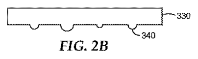
いくつかの実施形態において、微細構造は、谷部分とも称される、陥没部であってもよい。例えば、図2Aは、陥没した微細構造320又は微細構造くぼみを含む、微細構造層310の概略側面図である。微細構造化表面を形成する工具表面は一般に、複数の陥没部を含む。微細構造化拡散体の微細構造は通常、山部分とも称される、突出部である。例えば、図2Bは、突出した微細構造340を含む微細構造層330の概略側面図である。図8A〜図9D及び図15A〜図16Bは、複数の山及び山を囲む谷を含む例示の微細構造化表面の、様々な光学顕微鏡画像を示す。
In some embodiments, the microstructure may be a depression, also referred to as a valley. For example, FIG. 2A is a schematic side view of a
いくつかの実施形態において、微細構造は規則的なパターンを形成し得る。例えば、図3Aは、主表面415に規則的なパターンを形成する、微細構造410の概略平面図である。しかし、通常微細構造は不規則なパターンを形成する。例えば、図3Bは、不規則なパターンを形成する微細構造420の概略平面図である。場合によっては、微細構造は、ランダムに見える擬似ランダムパターンを形成し得る。
In some embodiments, the microstructure can form a regular pattern. For example, FIG. 3A is a schematic plan view of a
(例えば、個別の)微細構造は、傾きにより特徴付けられることができる。図4は、微細構造層140の一部の概略側面図である。特に、図4は主表面120内の微細構造160、及び対向する主表面142を示している。微細構造160は、微細構造の表面全体に亘る傾き分布を有する。例えば、微細構造は、位置510に傾きθを有し、θは、位置510における微細構造化表面に直交する法線520(α=90度)と、同一位置における微細構造化表面に対して正接となる接線530との間の角度である。傾きθは、接線530とマット層の主表面142との間の角度でもある。
Microstructures (eg, individual) can be characterized by a slope. FIG. 4 is a schematic side view of a part of the
いくつかの実施形態において、微細構造は実質的に(例えば、無機酸化物又はポリマー)マット粒子を含まない。しかし、マット粒子の不在下でも、微細構造70は、図1に示すように、(例えば、ジルコニア又はシリカ)ナノ粒子30を含む。
In some embodiments, the microstructure is substantially free of (eg, inorganic oxide or polymer) mat particles. However, even in the absence of matte particles,
ナノ粒子のサイズは、可視光線の顕著な光散乱を防止するように選択される。光学又は材料特性を最適化するため、及び全般的な組成物コストを低下させるために、複数の種類の無機酸化物粒子の混合物を用いることが望ましい場合がある。表面修飾コロイド状ナノ粒子は、少なくとも1nm又は5nmの(例えば非会合の)一次粒径又は会合粒径を有する無機酸化物粒子であり得る。一次又は会合粒径は一般に、100nm未満、75nm未満、又は50nm未満である。通常は、一次又は会合粒径は、40nm未満、30nm未満、又は20nm未満である。ナノ粒子は、非会合であることが好ましい。これらの測定値は、透過電子顕微鏡(TEM)に基づくことができる。表面修飾コロイド状ナノ粒子は、実質的に完全に凝縮可能である。 The size of the nanoparticles is selected to prevent significant light scattering of visible light. It may be desirable to use a mixture of multiple types of inorganic oxide particles to optimize optical or material properties and to reduce overall composition costs. The surface-modified colloidal nanoparticles can be inorganic oxide particles having a primary or associated (eg, non-associated) particle size of at least 1 nm or 5 nm. The primary or associated particle size is generally less than 100 nm, less than 75 nm, or less than 50 nm. Typically, the primary or associated particle size is less than 40 nm, less than 30 nm, or less than 20 nm. Preferably, the nanoparticles are non-associated. These measurements can be based on transmission electron microscopy (TEM). The surface-modified colloidal nanoparticles are substantially completely condensable.
完全凝縮ナノ粒子(シリカを除き)は通常、55%超、好ましくは60%超、より好ましくは70%超の結晶化度(独立金属酸化物粒子として測定した場合)を有する。例えば、結晶化度は、約86%以上の範囲であり得る。結晶化度は、X線回折法によって測定することができる。凝縮結晶性の(例えば、ジルコニア)ナノ粒子は、高い屈折率を有するが、非晶質ナノ粒子は通常、より低い屈折率を有する。 Fully condensed nanoparticles (except for silica) typically have a crystallinity (measured as independent metal oxide particles) of greater than 55%, preferably greater than 60%, more preferably greater than 70%. For example, the degree of crystallinity can be in the range of about 86% or more. The crystallinity can be measured by an X-ray diffraction method. Condensed crystalline (eg, zirconia) nanoparticles have a high refractive index, whereas amorphous nanoparticles typically have a lower refractive index.
ナノ粒子のサイズが実質的に小さいという理由から、このようなナノ粒子は微細構造を形成しない。むしろ、微細構造は、複数のナノ粒子を含む。 Such nanoparticles do not form a microstructure because the size of the nanoparticles is substantially small. Rather, the microstructure comprises a plurality of nanoparticles.
他の実施形態において、微細構造の一部分は、埋め込まれたマット粒子を含み得る。 In other embodiments, a portion of the microstructure may include embedded mat particles.
マット粒子は通常、約0.25マイクロメートル(250ナノメートル)越、又は約0.5マイクロメートル越、又は約0.75マイクロメートル越、又は約1マイクロメートル越、又は約1.25マイクロメートル越、又は約1.5マイクロメートル越、又は約1.75マイクロメートル越、又は約2マイクロメートル越の、平均サイズを有する。より小さいマット粒子は、比較的薄い微細構造層を含むマットフィルムにおいて、一般的である。しかしながら、微細構造層がより厚い実施形態では、マット粒子は、5マイクロメートル又は10マイクロメートルまでの平均サイズを有し得る。マット粒子の濃度は、少なくとも1又は2重量%〜約5、6、7、8、9、又は10重量%以上の範囲であり得る。 The matte particles are typically greater than about 0.25 micrometers (250 nanometers), or greater than about 0.5 micrometers, or greater than about 0.75 micrometers, or greater than about 1 micrometer, or about 1.25 micrometers. It has an average size of about 1.5 micrometers, or about 1.75 micrometers, or about 2 micrometers. Smaller matte particles are common in matte films that include relatively thin microstructured layers. However, in embodiments where the microstructure layer is thicker, the matte particles may have an average size of up to 5 or 10 micrometers. The concentration of the matte particles can range from at least 1 or 2% by weight to about 5, 6, 7, 8, 9, or 10% by weight or more.
図5は、基材850上に配設された微細構造層860を含む、光学フィルム800の概略側面図である。微細構造層860は、基材850に付着された第1の主表面810と、ポリマー結合剤840中に分散された複数のマット粒子830及び/又はマット粒子凝集体とを含む。いくつかの好ましい実施形態において、微細構造870のうちのかなりの部分、例えば少なくとも約50%、又は少なくとも約60%、又は少なくとも約70%、又は少なくとも約80%、又は少なくとも約90%には、マット粒子830又はマット粒子凝集体880が存在しない。すなわち、山の50%、40%、30%、20%、10%以下は、埋め込まれたマット粒子を含む。(例えば、シリカ又はCaCO3)マット粒子の存在は、以下に記載するように、これらのマット粒子の存在が所望の透明度、及びヘイズ特性を提供するのに不十分であったとしても、改善された耐久性を提供し得ることが推定される。しかしながら、マット粒子のサイズが比較的大きいため、コーティング組成物中に均一に分散されたマット粒子を維持することは困難であり得る。このことは、適用されたマット粒子の濃度に変動を生じる場合があり(特にウェブコーティングの場合)、これは次に(例えば、光学的)特性に変動を生じる。いくつかの実施形態では、実質的に微細構造化表面のすべての山は、(例えば、埋め込まれた)マット粒子を含まない。
FIG. 5 is a schematic side view of an
微細構造の少なくとも一部分が埋め込まれたマット粒子又は凝集マット粒子を含む実施形態では、マット粒子の平均サイズは通常、微細構造の平均サイズよりも十分小さく(例えば、少なくとも約2以上の因数により)、したがって図5に示すように、マット粒子が微細構造層の重合性樹脂組成物で包囲される。 In embodiments that include matte or agglomerated matte particles in which at least a portion of the microstructure is embedded, the average size of the matte particles is typically much smaller than the average size of the microstructure (eg, by a factor of at least about 2 or more), Therefore, as shown in FIG. 5, the mat particles are surrounded by the polymerizable resin composition of the fine structure layer.
マット層が埋め込まれたマット粒子を含む場合、マット層は通常、粒子の平均サイズよりも少なくとも約0.5マイクロメートル、又は少なくとも約1マイクロメートル、又は少なくとも約1.5マイクロメートル、又は少なくとも約2マイクロメートル、又は少なくとも約2.5マイクロメートル、又は少なくとも約3マイクロメートル大きい平均厚さ「t」を有する。 When the mat layer includes embedded mat particles, the mat layer is typically at least about 0.5 micrometer, or at least about 1 micrometer, or at least about 1.5 micrometer, or at least about 1.5 micrometer above the average size of the particles. It has an average thickness "t" that is 2 micrometers, or at least about 2.5 micrometers, or at least about 3 micrometers larger.
微細構造化表面は、任意の好適な作製方法により作製することができる。微細構造は通常、米国特許第5,175,030号(Luら)及び同第5,183,597号(Lu)に記載されているように、重合性樹脂組成物を工具表面と接触させて注型成型及び硬化させることにより、製作される。工具は、任意の利用可能な製作方法、例えば彫刻又はダイヤモンド切削を用いることにより製作することができる。例示的なダイヤモンド切削システム及び方法は、例えば、その開示が参照により本明細書に組み込まれる、国際出願公開第WO 00/48037号、並びに米国特許第7,350,442号及び同第7,328,638号に記載されている、高速工具サーボ(FTS)を含み及び使用し得る。 The microstructured surface can be made by any suitable method. The microstructure is typically achieved by contacting the polymerizable resin composition with a tool surface as described in US Pat. Nos. 5,175,030 (Lu et al.) And 5,183,597 (Lu). It is manufactured by casting and curing. The tool can be made by using any available manufacturing method, such as engraving or diamond cutting. Exemplary diamond cutting systems and methods are described, for example, in WO 00/48037, and U.S. Patent Nos. 7,350,442 and 7,328, the disclosures of which are incorporated herein by reference. , 638, may include and use a fast tool servo (FTS).
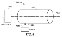
図6は、第1の微細構造化表面60を製造するために微細複製されることができる、工具の切削に使用可能な切削工具システム1000の概略側面図である。切削工具システム1000はねじ切り旋盤回転プロセスを用いたものであり、駆動装置1030によって中心軸1020を中心として回転及び/又は中心軸1020に沿って移動可能なロール1010、及びロール材料を切削するためのカッター1040を有している。カッターは、サーボ1050に装着され、駆動装置1060によってx方向に沿ってロールの中に、及び/又はロール沿いに移動させることができる。一般に、カッター1040はロール及び中心軸1020に対して垂直に取り付けられ、ロールが中心軸を中心として回転している間、ロール1010の彫刻可能な材料内に押し進められる。次いでカッターは中心軸に平行に送られて、ねじ切りが形成される。カッター1040は、高周波かつ低変位で同時に作動可能であり、微細複製時に微細構造をもたらす形体がロール内に製造される。
FIG. 6 is a schematic side view of a
サーボ1050は高速工具サーボ装置(FTS)であり、しばしばPZTスタックと呼ばれる、カッター1040の位置を速やかに調節する固体圧電(PZT)装置を有している。FTS 1050により、カッター1040のx方向、y方向、及び/若しくはz方向、又は軸外方向での高精度かつ高速での動作が可能になる。サーボ1050は、静止位置に対して制御された運動を生じさせることが可能な任意の高品質変位サーボであってよい。場合によっては、サーボ1050は、約0.1マイクロメートル以上の分解能で、0〜約20マイクロメートルの範囲の変位を繰り返し与えることが可能である。
駆動装置1060は、カッター1040をx方向に沿って中心軸1020に平行に移動させることができる。場合によっては、駆動装置1060の変位分解能は約0.1マイクロメートルを上回り、又は約0.01マイクロメートルを上回る。駆動装置1030によって生ずる回転運動が駆動装置1060によって生ずる並進運動と同期することによって、得られる微細構造の形状が正確に制御される。
The
ロール1010の彫刻可能な材料は、カッター1040によって彫刻可能な任意の材料であってよい。例示のロール材料には、銅などの金属、様々なポリマー、及び様々なガラス材料が挙げられる。
The engravable material of
カッター1040は任意の種類のカッターでよく、特定の用途において望ましい任意の形状を有し得る。例えば、図7Aは、半径「R」の弓形切削チップ1115を有するカッター1110の概略側面図である。場合によっては、切削チップ1115の半径Rは、少なくとも約100マイクロメートル、又は少なくとも約150マイクロメートル、又は少なくとも約200マイクロメートルである。いくつかの実施形態において、切削チップの半径Rは、又は少なくとも約300マイクロメートル、又は少なくとも約400マイクロメートル、又は少なくとも約500マイクロメートル、又は少なくとも約1000マイクロメートル、又は少なくとも約1500マイクロメートル、又は少なくとも約2000マイクロメートル、又は少なくとも約2500マイクロメートル、又は少なくとも約3000マイクロメートルである。
あるいは、工具の微細構造化表面は、図7Bに示すようなV形切削チップ1125を有するカッター1120、図7Cに示すような、部分的に直線状の切削チップ1135を有するカッター1130、又は7Dに示すような湾曲切削チップ1145を有するカッター1140を使用して、形成されてもよい。一実施形態において、少なくとも約178度以上の頂角βを有するV形切削チップを使用した。
Alternatively, the microstructured surface of the tool may be a
再び図6を参照すると、ロール材料の切削中に、ロール1010が中心軸1020に沿って回転し、カッター1040がx方向に沿って移動することにより、中心軸に沿ってピッチP1を有するねじ経路がロールの周囲に画定される。カッターがロール表面に垂直な方向に沿って移動してロール材料を切削するにつれて、カッターによって切削される材料の幅が、カッターの内外への移動又は突入と共に変化する。例えば図7Aを参照すると、カッターによる最大侵入深さは、カッターにより切削される最大幅P2に対応する。一般に、比P2/P1は約2〜約4の範囲内にある。
Referring again to FIG. 6, the screw having in the cutting of the roll material, to rotate the
あるいは、工具は、電着によって作製され得る。一実施形態において、第1の平均粗さを有する第1層の第1主表面をもたらす第1の電気メッキ工程を使用して金属を電着させることによって、金属の第1層を形成することと;第1の平均粗さより小さい第2の平均粗さを有する第2層の第2主表面をもたらす第2の電気メッキ工程を使用して第1主表面に金属を電着させることによって、金属の第2層を第1層の第1主表面上に形成することと;によって、工具は提供されて、これは国際特許第WO2014/081693号に記載されており、この開示は参照により本明細書に組み込まれる。 Alternatively, the tool can be made by electrodeposition. In one embodiment, forming the first layer of metal by electrodepositing the metal using a first electroplating step that results in a first major surface of the first layer having a first average roughness. By electrodepositing a metal on the first major surface using a second electroplating step that results in a second major surface of the second layer having a second average roughness less than the first average roughness; Forming a second layer of metal on the first major surface of the first layer; a tool is provided which is described in WO 2014/081693, the disclosure of which is hereby incorporated by reference. Incorporated in the specification.
いくつかの微細構造化拡散体は、4つの異なる工具の表面を微細複製することによって製造された。微細構造化表面は、工具表面の正確な複製物であったため、微細構造化表面層に関する今後の説明は、逆の工具表面の説明でもある。 Some microstructured diffusers have been manufactured by micro-replicating the surface of four different tools. Since the microstructured surface was an exact replica of the tool surface, any further description of the microstructured surface layer will be the opposite tool surface description.
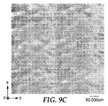
図8A、9A、15A、及び16Aは、4つの異なる工具(すなわち工具1〜工具4それぞれ)から生成される第1の微細構造化表面の共焦点スキャンレーザ顕微鏡画像(50倍対物レンズ)を示す。
FIGS. 8A, 9A, 15A, and 16A show confocal scanning laser microscope images (50 × objective) of a first microstructured surface generated from four different tools (ie,
第1の微細構造化表面を有する基材は、コーティングを第1の微細構造化表面に配設することによって、微細構造(例えば拡散体)物品を作製するための中間物品として、適切である。例えば、図8B〜8Dは、第1の微細構造化表面に配設された様々な厚みのコーティングを有する、図8Aの第1の微細構造化表面(工具1から形成される)を示す。図9B〜9Dは、第1の微細構造化表面に配設された様々な厚みのコーティングを有する、図9Aの第1の微細構造化表面(工具2から形成される)を示す。図15Bは、第1の微細構造化表面に配設された(例えば、3.3マイクロメートルの)コーティングを有する、図15Aの第1の微細構造化表面(工具3から形成される)を示す。図16Bは、第1の微細構造化表面に配設された(例えば、3.3マイクロメートルの)コーティングを有する、図16Aの第1の微細構造化表面(工具3から形成される)を示す。 A substrate having a first microstructured surface is suitable as an intermediate article for making a microstructured (eg, diffuser) article by disposing a coating on the first microstructured surface. For example, FIGS. 8B-8D show the first microstructured surface of FIG. 8A (formed from tool 1) with various thickness coatings disposed on the first microstructured surface. 9B-9D show the first microstructured surface of FIG. 9A (formed from tool 2) with various thickness coatings disposed on the first microstructured surface. FIG. 15B shows the first microstructured surface (formed from tool 3) of FIG. 15A with a coating (eg, 3.3 micrometers) disposed on the first microstructured surface. . FIG. 16B shows the first microstructured surface of FIG. 16A (formed from tool 3) having a coating (eg, 3.3 micrometers) disposed on the first microstructured surface. .
通常の実施形態において、コーティングは、山を被覆して、谷を部分的に満たす。しかしコーティングの粘度が十分低いとき、コーティングは谷を部分的に満たすと共に、一部の山だけを被覆できる。例えば、第1の微細構造化表面の最も高い山は、コーティングによって被覆できない。谷のこの部分的な充填が、第2の微細構造化表面を形成し、それも複数の山及び谷を有しており、コーティングと合わせて第1の微細構造化表面のトポグラフィから形成される。 In a typical embodiment, the coating covers the peaks and partially fills the valleys. However, when the viscosity of the coating is low enough, the coating can partially fill the valleys and cover only some peaks. For example, the highest peak of the first microstructured surface cannot be covered by the coating. This partial filling of the valley forms a second microstructured surface, which also has a plurality of peaks and valleys, formed from the topography of the first microstructured surface together with the coating .
コーティングの厚さは、第1の微細構造化表面及び所望される最終的な特性によって変化する。コーティングの厚さは通常、1/4波長の光学的厚さより大きい。国際特許第WO2011/140018号に記載のとおり、コーティングが1/4波長の光学的厚さを有するとき、物理的及び光学特性の実質的な変化が得られないように、コーティングは一般に、下にある第1の微細構造化表面に均一に適合する。(すなわち、乾燥した)コーティングの平均厚さは通常、少なくとも0.5、0.6、0.7、0.8、0.9、又は1マイクロメートルである。いくつかの実施形態では、(すなわち、乾燥した)コーティングの平均厚さは、少なくとも1.5、2、2.5、3、3.5、4、4.5、又は5マイクロメートルである。通常の実施形態において、コーティングの厚さは、約20、15、又は10マイクロメートル以下である。 The thickness of the coating will vary depending on the first microstructured surface and the final properties desired. The thickness of the coating is typically greater than the quarter wavelength optical thickness. As described in International Patent Publication No. WO2011 / 140018, when the coating has a quarter wavelength optical thickness, the coating is generally placed underneath so that no substantial change in physical and optical properties is obtained. Uniformly conforms to some first microstructured surface. The average thickness of the (ie, dried) coating is typically at least 0.5, 0.6, 0.7, 0.8, 0.9, or 1 micrometer. In some embodiments, the average thickness of the (ie, dried) coating is at least 1.5, 2, 2.5, 3, 3.5, 4, 4.5, or 5 micrometers. In typical embodiments, the thickness of the coating is no more than about 20, 15, or 10 micrometers.
第1及び第2の微細構造化表面は、少なくとも1つの光学又は物理的特性によって、それぞれ特徴付けられることが可能である。第1及び第2の微細構造化表面間の光学又は物理的な特性の差が、少なくとも10%の絶対値を有するとき、第2の微細構造化表面は、第1の微細構造化表面と実質的に異なると考えることができる。いくつかの実施形態では、物理的特性は、微細構造の補集合的累積傾き大きさ分布(すなわちFcc)、表面粗さ又は平均山高さであり得る。他の実施形態において、光学特性は、ヘイズ又は透明度であり得る。いくつかの実施形態では、第1及び第2の微細構造化表面間の光学又は物理的特性の差が、少なくとも15%又は20%以上の絶対値を有する。 The first and second microstructured surfaces can each be characterized by at least one optical or physical property. The second microstructured surface is substantially different from the first microstructured surface when the difference in optical or physical properties between the first and second microstructured surfaces has an absolute value of at least 10%. Can be considered different. In some embodiments, the physical property can be a complemental cumulative slope magnitude distribution (ie, Fcc), surface roughness, or average peak height of the microstructure. In other embodiments, the optical property can be haze or clarity. In some embodiments, the difference in optical or physical properties between the first and second microstructured surfaces has an absolute value of at least 15% or greater than 20%.
第1の微細構造化表面及び第2の微細構造化表面の代表的な部分は、第1の微細構造化表面に配設されたコーティングを更に含み、共焦点スキャンレーザ顕微鏡(50倍対物レンズ)を使用して画定される。 A representative portion of the first microstructured surface and the second microstructured surface further comprises a coating disposed on the first microstructured surface, and a confocal scanning laser microscope (50 × objective lens) Is defined using
Fcc(θ)は、傾きの大きさの補足的累積分布であり、以下の式により定義されて、式中、NG(q)は、q番目のアングルビンの画素数であり、各アングルビンは0.01度のサイズを有する。 F cc (θ) is the complementary cumulative distribution of the magnitude of the slope and is defined by the following equation, where NG (q) is the number of pixels of the q th angle bin, and The bin has a size of 0.01 degrees.

様々な例示の第1及び第2の微細構造層のFcc(θ)は、図10、図11及び図17に示されており、及び以下の表A〜Dで明らかにされる。各表A〜Dにおいて、括弧内の値は、第1の微細構造化表面(すなわち対照)と第2の微細構造化表面の差である。 F cc (θ) for various exemplary first and second microstructured layers are shown in FIGS. 10, 11 and 17, and are clarified in Tables AD below. In each of Tables AD, the value in parentheses is the difference between the first microstructured surface (ie, control) and the second microstructured surface.
表A〜Dの例示的実施形態に関して、0.1度超、0.3度超、0.7度超及び1.3度超の傾きの大きさでの第1の微細構造化表面の補集合的累積傾き大きさ分布は、少なくとも95、96、97、98、99、又は100%であり得る。0.1度超又は0.3度超の傾きの大きさでの第2の微細構造化表面の補集合的累積傾き大きさ分布は、少なくとも95、96、97、98、99、又は100%であり得る。いくつかの実施形態では、0.7度超の傾きの大きさでの第2の微細構造化表面の補集合的累積傾き大きさ分布は、少なくとも95、96、97、98、99、又は100%であり得、又は、それは、少なくとも85又は90%などわずかに低いこともあり得る。1.3度超の傾きの大きさでの第2の微細構造化表面の補集合的累積傾き大きさ分布は、少なくとも65、70、75、80、85、又は約90%であり得る。 For the exemplary embodiments of Tables A-D, complementation of the first microstructured surface with a magnitude of slope greater than 0.1 degrees, greater than 0.3 degrees, greater than 0.7 degrees, and greater than 1.3 degrees. The collective cumulative slope magnitude distribution can be at least 95, 96, 97, 98, 99, or 100%. The complementary cumulative slope magnitude distribution of the second microstructured surface at a slope magnitude greater than 0.1 degrees or greater than 0.3 degrees is at least 95, 96, 97, 98, 99, or 100%. Can be In some embodiments, the complementary cumulative slope magnitude distribution of the second microstructured surface at a slope magnitude greater than 0.7 degrees is at least 95, 96, 97, 98, 99, or 100. %, Or it can be slightly lower, such as at least 85 or 90%. The complementary cumulative slope magnitude distribution of the second microstructured surface at a slope magnitude greater than 1.3 degrees may be at least 65, 70, 75, 80, 85, or about 90%.
2.1度超又は4.1度超の傾きの大きさでの第1及び第2の微細構造化表面間の補集合的累積傾き大きさ分布の差は、少なくとも10%、11%、12%、13%、14%、又は15%である。更にいくつかの実施形態では、2.1度超又は4.1度超の傾きの大きさでの第1及び第2の微細構造化表面間の補集合的累積傾き大きさ分布の差は、少なくとも20%、30%、40%、50%、60%、又は70%である。 The difference in the complementary cumulative slope magnitude distribution between the first and second microstructured surfaces at a magnitude of the slope greater than 2.1 degrees or greater than 4.1 degrees is at least 10%, 11%, 12%. %, 13%, 14%, or 15%. Further, in some embodiments, the difference in the complementary cumulative slope magnitude distribution between the first and second microstructured surfaces at a slope magnitude greater than 2.1 degrees or greater than 4.1 degrees is: It is at least 20%, 30%, 40%, 50%, 60%, or 70%.
第1の微細構造化表面は、2.1度超の傾きの大きさでの補集合的累積傾き大きさ分布を少なくとも90%、91%、92%、93%、94%、95%、又は96%有することができる。しかしながら、第2の微細構造化表面は、80%以下の、及びいくつかの実施形態では、75、70、65、60、55、50、又は45%以下の、2.1度超の傾きの大きさでの補集合的累積傾き大きさ分布を有することができる。 The first microstructured surface has at least 90%, 91%, 92%, 93%, 94%, 95%, or at least 90%, 91%, 92%, 93%, 94%, 95%, or a complementary cumulative slope magnitude distribution with a slope magnitude greater than 2.1 degrees. 96%. However, the second microstructured surface has a slope of greater than 2.1 degrees, less than 80%, and in some embodiments less than 75, 70, 65, 60, 55, 50, or 45%. It can have a complementary cumulative slope magnitude distribution in magnitude.
第1の微細構造化表面は、4.1度超の傾きの大きさでの補集合的累積傾き大きさ分布を少なくとも60%、65%、70%、又は75%有することができる。しかしながら、第2の微細構造化表面は、4.1度超の傾きの大きさでの補集合的累積傾き大きさ分布を50、45、40、35、30、25、20、15、又は10%以下有することができる。 The first microstructured surface may have at least 60%, 65%, 70%, or 75% of the complementary cumulative slope magnitude distribution with a slope magnitude greater than 4.1 degrees. However, the second microstructured surface has a complementary cumulative slope magnitude distribution at slope magnitudes greater than 4.1 degrees, 50, 45, 40, 35, 30, 25, 20, 15, or 10 % Or less.
図10、図11及び図17の例示的実施形態に関して、第1の微細構造化表面は、10度超の傾きの大きさでの補集合的累積傾き大きさ分布を少なくとも10%、20%、30%、40%、又は50%有することができる。更に、第1の微細構造化表面は、15度超の傾きの大きさでの補集合的累積傾き大きさ分布を少なくとも5%、10%、15%、又は20%有することができる。しかし、第2の微細構造化表面は、10度超又は15度超の傾きの大きさでの補集合的累積傾き大きさ分布を40%、30%、又は20%未満、及びいくつかの実施形態では、10%、9%、8%、7%、6%、5%、4%、3%、2%、1%、又は0未満有することができる。更に、第1の微細構造化表面は、5度超の傾きの大きさでの補集合的累積傾き大きさ分布を少なくとも50%、60%、70%、80%、又は85%有することができる。しかし、第2の微細構造化表面は、5度超の傾きの大きさでの補集合的累積傾き大きさ分布を40%未満、及びいくつかの実施形態では、35%、30%、25%、20%、15%、10%、又は5%未満有することができる。 For the exemplary embodiments of FIGS. 10, 11 and 17, the first microstructured surface has a complementary cumulative slope magnitude distribution at slope magnitudes of greater than 10 degrees, at least 10%, 20%, It can have 30%, 40%, or 50%. Further, the first microstructured surface can have at least 5%, 10%, 15%, or 20% of the complementary cumulative slope magnitude distribution with a slope magnitude greater than 15 degrees. However, the second microstructured surface has a complementary cumulative slope magnitude distribution of less than 40%, 30%, or 20% with a magnitude of slope greater than 10 or 15 degrees, and in some implementations. In form, it can have less than 10%, 9%, 8%, 7%, 6%, 5%, 4%, 3%, 2%, 1%, or 0. Further, the first microstructured surface can have at least 50%, 60%, 70%, 80%, or 85% of the complementary cumulative slope magnitude distribution with a slope magnitude greater than 5 degrees. . However, the second microstructured surface has a complementary cumulative slope magnitude distribution of less than 40% at slope magnitudes greater than 5 degrees, and in some embodiments, 35%, 30%, 25% , 20%, 15%, 10%, or less than 5%.
補集合的累積傾き大きさ分布は、全体の補集合的累積傾き大きさ分布の構成要素である、x傾き及びy傾き大きさ分布に関して、表されることもできる。本明細書で使用する場合、「補集合的累積傾き大きさ分布」とは、特に明記しない限り、全体に関する。微細構造化表面の微細構造が幾何学的に対称であるとき、補集合的累積x傾き大きさ分布は、補集合的累積y傾き大きさ分布と実質的に同じである。図18及び図19の例示的実施形態に関して、例示の工具4から提供される第1の微細構造化表面は、補集合的累積y傾き傾き大きさ分布(Ycc)と実質的に同じである補集合的累積x勾配傾き大きさ分布(Xcc)を有するとして示される。それに対し、例示の工具3から提供される第1の微細構造化表面は非対称の微細構造を有し、したがって、x勾配及びy勾配分布は異なる。例えば、例示の工具3の5度超の工具3のYccは約70%であるが、Xccは、10、9、8、7、6、又は5%未満である。更に、例示の工具3について4.1度超の工具3のYccは70%超であるが、4.1度超のXccは、60、50、40、30、20、10、又は5%未満である。 The complementary cumulative slope magnitude distribution can also be expressed in terms of the x slope and y slope magnitude distributions that are components of the overall complement cumulative slope magnitude distribution. As used herein, “complementary cumulative slope magnitude distribution” refers to the entirety unless otherwise specified. When the microstructure of the microstructured surface is geometrically symmetric, the complementary cumulative x-slope magnitude distribution is substantially the same as the complementary cumulative y-slope magnitude distribution. With respect to the exemplary embodiment of FIGS. 18 and 19, the first microstructured surface provided from the exemplary tool 4 has a complement that is substantially the same as the complementary cumulative y-slope magnitude distribution (Ycc). Shown as having a collective cumulative x-gradient slope magnitude distribution (Xcc). In contrast, the first microstructured surface provided from the exemplary tool 3 has an asymmetric microstructure, and therefore the x and y gradient distributions are different. For example, Ycc of tool 3 greater than 5 degrees of exemplary tool 3 is about 70%, but Xcc is less than 10, 9, 8, 7, 6, or 5%. Further, for the exemplary tool 3, the Ycc of tool 3 greater than 4.1 degrees is greater than 70%, but the Xcc greater than 4.1 degrees is less than 60, 50, 40, 30, 20, 10, or 5%. It is.
第1及び第2の微細構造化表面は、平均高さ及び表面粗さ(例えばRa、Rz)を含む他の物理的特性に従って画定されることができる。Raは、測定された領域全体にわたって計算された平均粗さであり、Rzは、評価領域の10つの最大の山〜谷距離の平均最高表面高さである。例示の第1及び第2の微細構造層のRa及びRzは、以下の表E〜Hに記載される。各表E〜Hにおいて、括弧の値は、第1の微細構造化表面(すなわち対照)と第2の微細構造化表面の差であり、このような差は、パーセンテージ(例えば、Rz(第1)−Rz(第2)/Rz(第1))として表される。各表E〜Hで報告されるRz及び平均高さは、表面分析技術を利用して測定されるが、Rzは、コーティングされた第1の微細構造化表面の断面の走査電子顕微鏡から測定されることもできる。断面分析が利用されるとき、十分な数の断面が分析されて、第1及び第2の微細構造化表面全体を代表する統計学的に有意な結果を得る。 The first and second microstructured surfaces can be defined according to other physical properties, including average height and surface roughness (eg, Ra, Rz). Ra is the average roughness calculated over the entire measured area, and Rz is the average maximum surface height of the ten largest peak-to-valley distances of the evaluation area. Ra and Rz of the exemplary first and second microstructure layers are set forth in Tables EH below. In each of Tables E-H, the value in parentheses is the difference between the first microstructured surface (i.e., control) and the second microstructured surface, and such a difference is expressed as a percentage (e.g., Rz (first ) -Rz (second) / Rz (first)). The Rz and average height reported in each of Tables E-H are measured using surface analysis techniques, while Rz is measured from a scanning electron microscope of a cross section of the coated first microstructured surface. You can also. When cross-sectional analysis is utilized, a sufficient number of cross-sections are analyzed to obtain a statistically significant result representative of the entire first and second microstructured surfaces.
表E〜Hの実施形態に関して、第1の微細構造化表面に配設されたコーティングは、少なくとも10%の第2の微細構造化表面のRz及び/又はRaを低減できる。更に、いくつかの実施形態では、第1及び第2の微細構造化表面間のRz及び/又はRaの差は、少なくとも−20%、−30%、−40%、−50%、又は−60%であり得る。 With respect to the embodiments of Tables EH, a coating disposed on the first microstructured surface can reduce the Rz and / or Ra of the second microstructured surface by at least 10%. Further, in some embodiments, the difference in Rz and / or Ra between the first and second microstructured surfaces is at least -20%, -30%, -40%, -50%, or -60. %.
第2の微細構造化表面のRzは通常、少なくとも1.3、1.4、又は1.5マイクロメートル及び約5マイクロメートル以下であるが、第1の微細構造化表面は、第2の微細構造化表面より大きなRzを有する。いくつかの実施形態では、第2の微細構造化表面のRzは、少なくとも1.6、1.7、1.8、1.9、又は2マイクロメートルである。いくつかの実施形態において、第1の微細構造化表面のRzは、少なくとも4.5、5.0、5.5、6.0、6.5、7.0、7.5、8.0、8.5、9.0、9.5、又は10マイクロメートルであり得る。いくつかの実施形態では、第2の微細構造化表面のRzは、7.5、7.0、6.5、6.0、5.5、5.0、又は4.5マイクロメートル以下である。第2の微細構造化表面のRaは通常、少なくとも0.15、0.16、0.17、0.18、0.19、又は0.20マイクロメートル及び約1マイクロメートル以下であるが、第1の微細構造化表面は、第2の微細構造化表面より大きなRaを有する。いくつかの実施形態では、第2の微細構造化表面のRaは、0.95、0.90、0.85、0.80、又は0.75以下である。 The Rz of the second microstructured surface is typically at least 1.3, 1.4, or 1.5 micrometers and about 5 micrometers or less, while the first microstructured surface has a second microstructured surface. It has a higher Rz than the structured surface. In some embodiments, the second microstructured surface has an Rz of at least 1.6, 1.7, 1.8, 1.9, or 2 micrometers. In some embodiments, the first microstructured surface has an Rz of at least 4.5, 5.0, 5.5, 6.0, 6.5, 7.0, 7.5, 8.0. , 8.5, 9.0, 9.5, or 10 micrometers. In some embodiments, the second microstructured surface has an Rz of 7.5, 7.0, 6.5, 6.0, 5.5, 5.0, or 4.5 micrometers or less. is there. The Ra of the second microstructured surface is typically at least 0.15, 0.16, 0.17, 0.18, 0.19, or 0.20 micrometers and less than or equal to about 1 micrometer. One microstructured surface has a higher Ra than the second microstructured surface. In some embodiments, the Ra of the second microstructured surface is 0.95, 0.90, 0.85, 0.80, or 0.75 or less.
表E〜Hの実施形態に関して、第1の微細構造化表面に配設されたコーティングは、少なくとも10%の第2の微細構造化表面の平均高さを低減できる。更に、いくつかの実施形態では、第1及び第2の微細構造化表面間の平均高さの差は、少なくとも−20%、−30%、−40%、−50%、又は−60%であり得る。 With respect to the embodiments of Tables EH, the coating disposed on the first microstructured surface can reduce the average height of the second microstructured surface by at least 10%. Further, in some embodiments, the difference in average height between the first and second microstructured surfaces is at least -20%, -30%, -40%, -50%, or -60%. possible.
第2の微細構造化表面の平均高さは通常、少なくとも0.75、0.80、0.85、0.90、0.95、又は1.00マイクロメートルである。いくつかの実施形態では、第2の微細構造化表面の平均高さは、少なくとも1.5、又は2.0マイクロメートルである。第2の微細構造化表面の平均高さは通常、約4マイクロメートル以下であり、及びいくつかの実施形態では、3.5又は3マイクロメートル以下である。第1の微細構造化表面は、第2の微細構造化表面より大きい平均高さを有する。いくつかの実施形態では、第1の微細構造化表面の平均高さは、少なくとも2.5、3、3.5、4、又は5マイクロメートルである。 The average height of the second microstructured surface is typically at least 0.75, 0.80, 0.85, 0.90, 0.95, or 1.00 micrometers. In some embodiments, the average height of the second microstructured surface is at least 1.5, or 2.0 micrometers. The average height of the second microstructured surface is typically no greater than about 4 micrometers, and in some embodiments no greater than 3.5 or 3 micrometers. The first microstructured surface has an average height that is greater than the second microstructured surface. In some embodiments, the average height of the first microstructured surface is at least 2.5, 3, 3.5, 4, or 5 micrometers.
第1及び第2の微細構造化表面のヘイズ及び透明度は、実施例に記載されている試験方法に従って測定できる。様々な例示の第1及び第2の微細構造層のヘイズ及び透明度が、以下の表I〜Jに記載される。各表I〜Jにおいて、括弧内の値は、第1の微細構造化表面(すなわち対照)と第2の微細構造化表面の差である。補集合的累積傾き大きさ分布は、第1の微細構造化表面を作製するために利用される重合性樹脂の選択に影響を受けないが、重合性樹脂の選択はヘイズ及び透明度に影響を及ぼすことができる。2つの異なる重合性樹脂が、第1の微細構造化表面を作製するために利用され、以下の表I〜Jに示すように、1つが1.56の屈折率(RI)を有し、残りの1つが1.65の屈折率を有する。 The haze and transparency of the first and second microstructured surfaces can be measured according to the test methods described in the examples. The haze and clarity of various exemplary first and second microstructured layers are set forth in Tables IJ below. In each of Tables I-J, the value in parentheses is the difference between the first microstructured surface (ie, control) and the second microstructured surface. The complementary cumulative slope magnitude distribution is not affected by the choice of polymerizable resin used to create the first microstructured surface, but the choice of polymerizable resin affects haze and clarity. be able to. Two different polymerizable resins were utilized to create the first microstructured surface, one having a refractive index (RI) of 1.56 and the remaining as shown in Tables IJ below. Has a refractive index of 1.65.
表I〜Jの例示的実施形態に関して、第1及び第2の微細構造化表面間のヘイズの差は、少なくとも10%であり得る。更に、いくつかの実施形態では、第1及び第2の微細構造化表面間のヘイズの差は、少なくとも20%、30%、40%、50%、60%、又は70%であり得る。 For the exemplary embodiments of Tables IJ, the difference in haze between the first and second microstructured surfaces can be at least 10%. Further, in some embodiments, the difference in haze between the first and second microstructured surfaces can be at least 20%, 30%, 40%, 50%, 60%, or 70%.
第1の微細構造化表面は、少なくとも60、70、80、又は90%のヘイズを有することができる。しかし、第2の微細構造化表面は、50、45、40、35、30、25、20、15、又は10%以下のヘイズを有することができる。いくつかの実施形態では、ヘイズは、10、9、8、7、6、5、4、3、又は2%未満である。 The first microstructured surface can have a haze of at least 60, 70, 80, or 90%. However, the second microstructured surface can have a haze of 50, 45, 40, 35, 30, 25, 20, 15, or 10% or less. In some embodiments, the haze is less than 10, 9, 8, 7, 6, 5, 4, 3, or 2%.
表I〜Jの例示的実施形態に関して、第1及び第2の微細構造化表面間の透明度の差は、少なくとも−10%であり得る。更に、第1及び第2の微細構造化表面間の透明度の差は、少なくとも−20%、−25%、−30%、−35%、又は−40%であり得る。 For the exemplary embodiments of Tables I-J, the difference in transparency between the first and second microstructured surfaces can be at least -10%. Further, the difference in transparency between the first and second microstructured surfaces can be at least -20%, -25%, -30%, -35%, or -40%.
第1の微細構造化表面は、少なくとも10、9、8、7、6、又は5%の透明度を有することができる。しかし、第2の微細構造化表面は、少なくとも15、20、25、30、35、40、又は45%の透明度を有することができる。 The first microstructured surface can have at least 10, 9, 8, 7, 6, or 5% transparency. However, the second microstructured surface can have at least 15, 20, 25, 30, 35, 40, or 45% transparency.
第1の微細構造化表面に配設されたコーティングを含む微細構造化拡散体は、様々な光学フィルムで利用できる。 Microstructured diffusers that include a coating disposed on a first microstructured surface are available in various optical films.
いくつかの実施形態では、微細構造化拡散体は更に、図12で示すように、第1及び第2の微細構造化表面層に対向する主表面上のプリズム構造を含む。すなわち、(例えば第1の)微細構造化表面は、基材とプリズム層との間に埋め込まれない。しかし、別の実施形態では、第1の微細構造化表面に配設されたコーティングを含む微細構造化拡散体は、基材とプリズム層との間に埋め込まれることが可能であり、これは国際特許第WO2013/158475号に記載されており、この開示は参照により本明細書に組み込まれる。 In some embodiments, the microstructured diffuser further includes a prismatic structure on the major surface opposite the first and second microstructured surface layers, as shown in FIG. That is, the (eg, first) microstructured surface is not embedded between the substrate and the prism layer. However, in another embodiment, a microstructured diffuser that includes a coating disposed on a first microstructured surface can be embedded between a substrate and a prism layer, which is It is described in patent WO2013 / 158475, the disclosure of which is incorporated herein by reference.
微細構造(例えば拡散体)層の微細構造は、主に光学利得を提供するように設計された光学フィルムの(例えばプリズム)構造とは、異なる。一態様では、微細構造(例えば拡散体)層の微細構造は、ランダムに見える不規則なパターン、又は擬似ランダムパターンを形成する。それに対し、光学フィルムの(例えばプリズム)構造は一般に、表面上規則的なパターンを有する。別の態様において、微細構造(例えば拡散体)層の微細構造は通常、光学フィルムの(例えばプリズム)構造より小さい。例えば、微細構造(例えば拡散体)層の微細構造は通常、8マイクロメートル以下の山〜谷の平均高さを有するが、(例えばプリズム)構造は通常、8、9、又は10マイクロメートル超の山〜谷の平均高さを有する。別の態様においては、光学フィルムの(例えばプリズム)構造は、実質的に同じ傾き(例えば約90度の頂角)を有するが、微細構造(例えば拡散体)層は、前述したように傾きの異なる大きさを有する微細構造を有する。多くの実施形態において、微細構造化拡散体の微細構造の少なくとも90%は、20又は15度未満の傾きの大きさを有する。 The microstructure of the microstructure (eg, diffuser) layer is different from the (eg, prism) structure of an optical film designed to provide primarily optical gain. In one aspect, the microstructure of the microstructure (eg, diffuser) layer forms a random-looking, irregular pattern, or a pseudo-random pattern. In contrast, optical film (eg, prism) structures generally have a regular pattern on the surface. In another embodiment, the microstructure of the microstructure (eg, diffuser) layer is typically smaller than the (eg, prism) structure of the optical film. For example, the microstructure of the microstructure (e.g., diffuser) layer typically has an average peak-to-valley height of 8 micrometers or less, while the (e.g., prism) structure typically has an average height of more than 8, 9, or 10 micrometers. It has an average peak-to-valley height. In another embodiment, the (eg, prism) structure of the optical film has substantially the same tilt (eg, about 90 degrees apex angle), but the microstructure (eg, diffuser) layer has a tilt as described above. It has microstructures with different sizes. In many embodiments, at least 90% of the microstructures of the microstructured diffuser have a slope magnitude of less than 20 or 15 degrees.
図12は、入射光線を所望の方向に方向転換するための、光方向転換フィルム100の概略側面図である。光方向転換フィルム100は、y方向に沿って延在する複数の微細構造150を含む、第1の主表面110を含む。微細構造150がプリズムであるとき、前記微細構造層はプリズム層と言われることができる。光方向転換フィルム100は、第1の主表面110と反対側の第2の主要面120も含み、及び、第1の微細構造層60と、第1の微細構造化表面に配設されたコーティングとを含み、前記コーティングが谷を部分的に満たして、第2の微細構造化表面122を形成する。
FIG. 12 is a schematic side view of a
また、光方向転換フィルム100は、対応する第1の主表面110と第2の主表面120との間に配設され、第1の主表面172と、反対側にある第2の主表面174と、を含む基材層170を含む。また、光方向転換フィルム100は、基材層の第1の主表面172に配設され、光方向転換フィルムの第1の主表面110を含むプリズム層130と、基材層の第2の主表面174に配設され、光方向転換フィルムの第2の主表面174を含むマット層140と、を含む。マット層は、主表面120の反対側にある主表面142を有する。
In addition, the
例示の光方向転換フィルム100は、3つの層130、170、及び140を含む。一般に、光方向転換フィルムは1つ以上の層を有してよい。例えば、場合によっては、光方向転換フィルムは、対応する第1の主表面110と、第2の主表面120と、を含む単一層を有してよい。別の例としては、場合によっては、光方向転換フィルムは多数の層を有してよい。例えば、かかる場合、基材170は多数の層を有してよい。
The exemplary
微細構造150は、主として光方向転換フィルムの主表面120への入射光線を、正のz方向に沿うなど所望の方向に沿って方向転換するように設計されている。例示の光方向転換フィルム100では、微小構造150はプリズム線状構造である。一般に、微小構造150は、例えば、入射光線の一部を屈折させ、入射光線の別の一部を再利用することによって光を方向転換できる任意の種類の微小構造であってよい。例えば、微小構造150の断面形状は、湾曲部及び/若しくは部分的線状部である、又はこれらを含んでよい。例えば、場合によっては、微細構造150は、y方向に沿って延在する、線状円柱レンズであってよい。
The
各線状プリズム微細構造150は、頂角152と、例えば主平面172などの共通基準面から測定された高さ154と、を含む。光結合若しくはウェットアウトを低減させること、及び/又は光方向転換フィルムの耐久性を向上させることが望ましいなど、場合によっては、プリズム微細構造150の高さは、y方向に沿って変化してよい。例えば、プリズム線状微細構造151のプリズム高さは、y方向に沿って変化する。かかる場合、プリズム微細構造151は、y方向に沿って変化する局所的高さと、最大高さ155と、平均高さと、を有する。場合によっては、線状微細構造153などプリズム線状微細構造は、y方向に沿って一定高さを有する。かかる場合、微細構造は、最大高さ及び平均高さと等しい、一定の局所的高さを有する。
Each
実効透過率(ET)は、図2に示す光学系を使用して測定することができ、参照により本明細書に組み込まれる国際特許第WO2010/141262号に記載される。 Effective transmission (ET) can be measured using the optics shown in FIG. 2 and is described in International Patent Publication No. WO 2010/141262, which is incorporated herein by reference.
光結合又はウェットアウトを低減させることが望ましいなど場合によっては、一部の線状微細構造は低く、一部の線状微細構造は高い。例えば、線状微細構造153の高さ156は、線状微細構造157の高さ158よりも小さい。
In some cases, such as where it is desirable to reduce optical coupling or wetout, some linear microstructures are low and some linear microstructures are high. For example, the
頂角、つまり二面角152は、用途において望ましい可能性がある任意の値を有することができる。例えば、場合によっては、頂角152は、約70度〜約110度、又は約80度〜約100度、又は約85度〜約95度の範囲であってよい。場合によっては、微細構造150は等しい頂角を有してよく、これは、例えば、約88度又は89度〜90度など約92度又は91度の範囲であってよい。
The apex angle, or
プリズム層130は、特定の用途において望ましい任意の屈折率を有し得る。例えば場合によっては、プリズム層の屈折率は、約1.4〜約1.8、又は約1.5〜約1.8、又は約1.5〜約1.7の範囲である。場合によっては、プリズム層の屈折率は、約1.5以上、又は約1.55以上、又は約1.6以上、又は約1.65以上、又は約1.7以上である。
光方向転換フィルム100が液晶ディスプレイシステムで用いられるなど場合によっては、光方向転換フィルム100は、ディスプレイの輝度を増大させる、つまり向上させることができる。こうした場合では、光方向転換フィルムは、1よりも大きな実効透過率又は相対利得を有する。本明細書で使用する場合、実効透過率とは、フィルムが所定位置にないディスプレイの輝度に対する、フィルムがディスプレイシステムの定位置に配されたディスプレイシステムの輝度の比のことである。
In some cases, such as when the
光方向転換フィルム100が、輝度を増大させるためにディスプレイシステムで用いられ、線状プリズムが約1.6を超える屈折率を有するなど場合によっては、光方向転換フィルムの平均実効透過率(ETA)は、約1.5以上、又は約1.55以上、又は約1.6以上、又は約1.65以上、又は約1.7以上、又は約1.75以上、又は約1.8以上、又は約1.85以上である。
In some cases, the
他の場合では、2つの光方向転換フィルムの積層体が輝度を増加させるためにディスプレイシステムで用いられるとき(例えば図14に示される)など、平均実効透過率(ETA)は少なくとも1.9、2.0、又は2.1であり得、2.4、2.5、又は2.6まで変動できる。 In other cases, such as when a stack of two light redirecting films is used in a display system to increase brightness (eg, as shown in FIG. 14), the average effective transmission (ETA) is at least 1.9; It can be 2.0, or 2.1, and can vary up to 2.4, 2.5, or 2.6.
第2の微細構造化表面122は、主として、光方向転換フィルムによる光の方向転換機能及び輝度向上機能に悪影響を及ぼさない、又はほとんど及ぼさずに、望ましくない物理的欠陥(例えば、キズなど)及び/又は光学的欠陥(例えば、ディスプレイ若しくは照明システムのランプによる、望ましくない輝点、つまり「ホット」スポット、又は、しばしばモアレと呼ばれるパターンの特別な干渉)を隠蔽することを目的として設計される。
The second
本明細書に記載されるように、微細構造化拡散体を含む光学フィルムは、種々の光学フィルム積層体で利用できる。いくつかの実施形態では、光学フィルム積層体は、利得及び非プリズム微細構造化拡散体を増加させるように設計された、単一の光配向(例えばプリズム)フィルムを含む。他の実施態様において、光学積層体は、利得を増加させるように設計された、少なくとも2つの光配向(例えばプリズム)フィルムを含む。プリズムフィルムは通常、第1のプリズムフィルムの頂点が第2のプリズムフィルムの頂点と直交するように、積み重ねられる。一実施形態において、光学フィルム又は光学フィルム積層体は、光学不活性結合部分を含み、これは例えば、国際特許第WO2011/130155号、同第WO2011/130144号、同第WO2011/130151号、及び同第WO 2013/138495に記載されている。 As described herein, an optical film including a microstructured diffuser can be utilized in various optical film laminates. In some embodiments, the optical film stack includes a single light directing (eg, prism) film designed to increase gain and non-prism microstructured diffuser. In another embodiment, the optical stack includes at least two light directing (eg, prism) films designed to increase gain. The prism films are typically stacked such that the apex of the first prism film is orthogonal to the apex of the second prism film. In one embodiment, the optical film or optical film laminate comprises an optically inactive bonding portion, such as, for example, International Patent Publication Nos. WO2011 / 130155, WO2011 / 130144, WO2011 / 130151, and WO2011 / 130151. WO 2013/138495.
光学不活性結合部分を含む1つの例示の光学フィルムが、図13に示される。光配向フィルム4400は、第1の複数の線状対称な一体型個別構造4420と、第2の複数の線状対称な個別構造4460とを含む。構造4420及び4460をy方向に沿って延在させ、基材4410上に配設した。基材4410は、厚さ約29マイクロメートル及び屈折率約1.65のPETで作製した。硬化済み構造4420及び4460の屈折率は、約1.56であった。各一体型個別構造に、主に光配向フィルムを表面に結合するように設計される結合部分4430を備え、主に光を方向付け、再利用するように設計される光配向部分4440上に配設した。個別構造4460は任意の結合部分を含まず、主に光を方向付け、再利用するように設計された。一体型個別構造4420を個別構造4460と交互に配設した。
One exemplary optical film that includes an optically inactive binding moiety is shown in FIG. The
各結合部分4430は、xy平面(光配向フィルムの平面)と、約80〜85度である角度ω1をなした2つの対向する側部小平面4432を含む。各結合部分は、最小基部寸法t2が約1.5(±0.5)マイクロメートルで、最大高さt1が約4(±0.5)マイクロメートルの基部4434を有した。各結合部分は、最小上面寸法t3が約0.2(±0.2)マイクロメートルの湾曲した又は丸形の上面も備えた。各光配向部分4420は、xy平面(光配向フィルムの平面)と約45度の角度ω2をなした2つの対向する側部小面4442を備えた。各光配向部分は、最小基部寸法t5が約24マイクロメートルで、最大高さt4が約12マイクロメートルの基部4444を有した。一体型個別構造4420の結合部分4430の頂部と、個別構造4460の頂部との間のz軸オフセット高さの差は、2.6マイクロメートルであった。光配向フィルム4400の平均実効透過率ETAは、約1.63であった。
Each
光学不活性結合部分を含む他の適切な例示の光学フィルムは、国際特許第WO 2012/138495号に記載されており、この開示は参照により本明細書に組み込まれる。 Other suitable exemplary optical films that include an optically inactive binding moiety are described in International Patent Publication No. WO 2012/138495, the disclosure of which is incorporated herein by reference.
図13の光学フィルムは、図14に示すように光学フィルム積層体に含まれることができ、図14は、光配向フィルム(例えばプリズム)2010上に任意追加的に配設される、本明細書に記載される第1及び第2の微細構造化表面2090を含む光学フィルムを含有する光学積層体2000の概略側面図である。光配向フィルム2010は、第1の構造主表面2020と、対向する第2の主表面2025とを含む。第1の構造主表面2020は、基材2005上に配設される複数の一体型個別構造2030を含む。少なくとも一部の一体型個別構造はそれぞれ、主に光を方向付けするための光配向部分2040と、主に光配向フィルムを光学フィルム2090に結合するための結合部分2050とを備える。代表的な光学積層体2000の場合などのいくつかの場合において、光配向フィルム2010少なくとも一部の結合部分2050の少なくとも一部分が、光学フィルム2090に貫入し、光配向フィルム2010の少なくとも一部の光配向部分2040の少なくとも一部分は、光学フィルム2090に貫入しない。そのような場合、光学積層体2000は、光配向フィルム2010と光学フィルム2090との間に複数の未充填空隙2015を含み、ここで未充填空隙は、空気及び/又はガスを含んでよい。場合によっては、複数の未充填空隙2015のうち少なくとも一部はそれぞれ、光学フィルム2090、及び2つ以上の隣接する一体型個別構造2030の部分によって画定される領域(一体型個別構造2030は光学フィルムに貫入せず、この領域を直接取り巻く)を実質的に占める。例えば、そのような場合、未充填空隙は、光学フィルム2090、及び光学フィルムに貫入しない2つ以上の隣接する一体型個別構造2030の部分によって画定される領域の少なくとも50%、又は少なくとも60%、又は少なくとも70%、又は少なくとも80%、又は少なくとも90%を占める。例えば、線状一体型個別構造2030の場合、未充填空隙2015は、光学フィルム2090の上面、線状一体型個別構造2030Aの、光学フィルムに貫入していない右側部分2021、線状一体型個別構造2030Bの、光学フィルムに貫入していない左側部分2022によって画定される領域を実質的に占める。
The optical film of FIG. 13 can be included in an optical film stack, as shown in FIG. 14, and FIG. FIG. 9 is a schematic side view of an
光学フィルム2090は、任意追加的に(例えばプリズム)光学層2070を更に含む光透過性基材、任意追加的に光透過性基材2070に配設されるプライマー層2075、及び任意追加的のプライマー層2075に配設されたコーティング(例えば光学接着剤)層2060を含む。プライマー層が存在しないとき、コーティング2060は、直接光学フィルム2090の第1の微細構造化表面2076に配設される。光配向フィルム2010の結合部分2050の、光学フィルムに貫入する一部は、コーティング(例えば光学接着剤)層に貫入する。コーティング(例えば光学接着剤)層2060は、大気環境又は光配向部分2040の周囲環境を実質的に維持しながら、光配向フィルム2010を光学層2070又は光学層2070の主表面2071に付着又は結合する。場合によっては、結合部分2050が高いアスペクト比を有し、光学フィルム2090と光配向フィルム2010との間に強い結合をもたらすことができる。
The
光学接着剤層に貫入する結合部分2050は、平均最大高さh2,avgを有するが、これは、光学接着剤層に貫入した個々の結合部分の最大高さh2の平均である。場合によっては、h2,avgは、光学接着剤層2060の平均厚さh3よりも大きい。例えば、そのような場合、h2,avgは、h3よりも少なくとも0.2マイクロメートル、又は少なくとも0.3マイクロメートル、又は少なくとも0.4マイクロメートル、又は少なくとも0.5マイクロメートル、又は少なくとも0.7マイクロメートル、又は少なくとも1マイクロメートル、又は少なくとも1.2マイクロメートル、又は少なくとも1.5マイクロメートル、又は少なくとも1.7マイクロメートル、又は少なくとも2マイクロメートル大きい。
Binding
個々の結合部分の平均高さがコーティング(例えば光学接着剤)層の平均厚さh3よりも大きいとき、結合部分の高さによって、構造体の光学活性部分と接着剤層との間に物理的隔離部が生じ得る。この隔離部又は空気界面は維持される又は実質的に不変であるが、ただし、積層体の通常使用間に接着剤組成物が流動しない、又は「クリープ変形」しないことを条件とする。このような使用は、高温における、所望により高湿と組み合わせる経年変化試験の利用によってシミュレーションできる。 When the average height of the individual binding moieties is greater than the average thickness h 3 of the coating (e.g., optical adhesive) layer, the height of the binding moiety, physical between the optically active portion of the structure the adhesive layer A separation may occur. This isolator or air interface is maintained or substantially unchanged, provided that the adhesive composition does not flow or "creep" during normal use of the laminate. Such use can be simulated by the use of aging tests at elevated temperatures, optionally in combination with high humidity.
あるいは、個々の結合部分の平均高さがコーティング(光学接着剤)層の平均厚さh3より小さいとき、貫入深さ、及び積層体の通常使用間にかかる貫入率を維持することによって、構造体の光学活性分と接着剤層との間に隔離部を設ける。 Alternatively, when the average height of the individual binding moieties is less than the average thickness h 3 of the coating (optical adhesive) layer, by maintaining penetration depth, and usually takes penetration rate between use of the laminate structure An isolator is provided between the optically active component of the body and the adhesive layer.
一実施形態において、コーティング(例えば光学接着剤)層は、約3〜6マイクロメートルの平均厚さh3を有し、結合部分は、約4マイクロメートルの平均最大高さh2,avgを有する。 In one embodiment, the coating (e.g., optical adhesive) layer has an average thickness h 3 of about 3-6 micrometers, the binding moiety has an average maximum height h 2, avg of about 4 micrometers .
一般に、光学フィルム基材2070は任意の光学層を含み、及び、ある用途に所望され得る任意の機能を提供し得る。例えば、場合によっては、基材は、主に他の層の支持体を提供してよい。別の例として、開示される基材は、例えば、反射偏光子若しくは吸収偏光子を備えて偏光する、光学拡散体を備えて光を拡散する、光配向フィルムを備えて光を方向付ける、又は向きを変えることができる。
In general, the
第1の微細構造化表面層は通常、重合性樹脂の反応生成物などのポリマー材料を含む。様々なフリーラジカル重合性(例えば(メタ)アクリレート)モノマー、オリゴマー、ポリマー、及びこれらの混合物を、第1の微細構造化表面層の有機材料中に用いることができる。いくつかの実施形態では、重合性樹脂は更に、無機酸化物ナノ粒子を含む。 The first microstructured surface layer typically includes a polymer material, such as a reaction product of a polymerizable resin. Various free radically polymerizable (eg, (meth) acrylate) monomers, oligomers, polymers, and mixtures thereof can be used in the organic material of the first microstructured surface layer. In some embodiments, the polymerizable resin further comprises inorganic oxide nanoparticles.
第1の微細構造層の重合性組成物は通常、2つの(メタ)アクリレート基(すなわち、ジ(メタ)アクリレートモノマー)を有する、少なくとも1つの芳香族(メタ)アクリレートモノマーを含む。芳香族ジ(メタ)アクリレートモノマーの量は通常、少なくとも5重量%であり、及び80重量%以下である。重合性樹脂が無機酸化物ナノ粒子を含まないとき、芳香族ジ(メタ)アクリレートモノマーの量は通常、少なくとも10、15、20、又は25重量%以上である。重合性樹脂が更に無機酸化物ナノ粒子を含むとき、芳香族ジ(メタ)アクリレートモノマーの量は、25重量%を超えない。 The polymerizable composition of the first microstructure layer typically includes at least one aromatic (meth) acrylate monomer having two (meth) acrylate groups (ie, di (meth) acrylate monomer). The amount of aromatic di (meth) acrylate monomer is usually at least 5% by weight and not more than 80% by weight. When the polymerizable resin does not include inorganic oxide nanoparticles, the amount of aromatic di (meth) acrylate monomer is typically at least 10, 15, 20, or 25 wt% or more. When the polymerizable resin further comprises inorganic oxide nanoparticles, the amount of aromatic di (meth) acrylate monomer does not exceed 25% by weight.
いくつかの実施形態では、ジ(メタ)アクリレートモノマーは、ビスフェノールAから誘導される。1つの代表的なビスフェノールAエトキシル化ジアクリレートモノマーは、Sartomerより、商標名「SR602」(20℃で610cpsの粘度、及び2℃のガラス転移温度(Tg)を有すると報告されている)で市販されている。別の代表的なビスフェノールAエトキシル化ジアクリレートモノマーは、Sartomerから商標名「SR601」(20℃において、粘度1080cps、及びTg 60℃を有すると報告されている)にて市販されている。米国特許第7,282,272号に記載されているものなど、様々な他のビスフェノールAモノマーが当技術分野にて記載されている。 In some embodiments, the di (meth) acrylate monomer is derived from bisphenol A. One representative bisphenol A ethoxylated diacrylate monomer is commercially available from Sartomer under the trade name “SR602” (reported to have a viscosity of 610 cps at 20 ° C. and a glass transition temperature (Tg) of 2 ° C.). Have been. Another representative bisphenol A ethoxylated diacrylate monomer is commercially available from Sartomer under the trade name "SR601" (reported to have a viscosity of 1080 cps at 20C and a Tg of 60C). Various other bisphenol A monomers have been described in the art, such as those described in U.S. Patent No. 7,282,272.
他の実施態様において、重合性組成物は、ビスフェノールAから誘導されるモノマーを含まない。1つの好適な二官能性芳香族(メタ)アクリレートモノマーは、ビフェニルジ(メタ)アクリレートモノマーであり、これは米国特許第2008/0221291号に記載されていて、この開示は参照により本明細書に組み込まれる。ビフェニルジ(メタ)アクリレートモノマーは、以下の一般式を有し得る。 In another embodiment, the polymerizable composition does not include a monomer derived from bisphenol A. One suitable difunctional aromatic (meth) acrylate monomer is a biphenyl di (meth) acrylate monomer, which is described in U.S. Patent No. 2008/0221291, the disclosure of which is hereby incorporated by reference. Be incorporated. The biphenyl di (meth) acrylate monomer may have the following general formula:
各R2は独立してBrであり、
mは、0〜4の範囲であり、
各Qは独立してO又はSであり、
nは0〜10の範囲であり、
Lは、1つ以上のヒドロキシル基で任意追加的に置換されたC2〜C12のアルキレン基であり、
zは、芳香環であり、及び、
tは独立して0又は1である。
Each R2 is independently Br;
m ranges from 0 to 4,
Each Q is independently O or S;
n ranges from 0 to 10,
L is a C2-C12 alkylene group optionally substituted with one or more hydroxyl groups,
z is an aromatic ring, and
t is independently 0 or 1.
−Q[L−O]nC(O)C(R1)=CH2基の少なくとも一方、好ましくは両方は、モノマーが25℃で液体であるように、オルト又はメタ位で置換されている。
-Q at least one of the [L-O] nC (O ) C (R1) =
いくつかの実施形態において、二官能性芳香族(メタ)アクリレートモノマーは、450g/モル未満の分子量を有し、かつ少なくとも1.50、1.51、1.52、1.53、1.54、1.55、1.56、1.57、又は1.58の屈折率を有する芳香族モノ(メタ)アクリレートモノマーと組み合わされる。前記反応性希釈剤は通常、フェニル、ビフェニル、又はナフチル基を含む。更に、このような反応性希釈剤は、ハロゲン化されてもよく、又は非ハロゲン化(例えば非臭素化)されてもよい。反応性希釈剤の含有により、有機成分の屈折率の上昇、及び粘度の低減による重合性組成物の加工性の改善が、同時に可能になる。 In some embodiments, the bifunctional aromatic (meth) acrylate monomer has a molecular weight of less than 450 g / mol and at least 1.50, 1.51, 1.52, 1.53, 1.54 , 1.55, 1.56, 1.57, or 1.58 in combination with an aromatic mono (meth) acrylate monomer. The reactive diluent typically contains a phenyl, biphenyl, or naphthyl group. Further, such reactive diluents may be halogenated or non-halogenated (eg, non-brominated). The inclusion of the reactive diluent simultaneously increases the refractive index of the organic component and improves the processability of the polymerizable composition by reducing the viscosity.
芳香族モノ(メタ)アクリレート反応性希釈剤の濃度は通常、少なくとも5、6、7、8、9、又は10重量%である。いくつかの実施形態では、芳香族モノ(メタ)アクリレート反応性希釈剤の濃度は、重合性樹脂組成物の50、40、又は30重量%以下である。 The concentration of the aromatic mono (meth) acrylate reactive diluent is usually at least 5, 6, 7, 8, 9, or 10% by weight. In some embodiments, the concentration of the aromatic mono (meth) acrylate reactive diluent is no more than 50, 40, or 30% by weight of the polymerizable resin composition.
好適な反応希釈剤としては、国際特許WO2008/112451号に記載のとおり、例えば、種々のビフェニル(メタ)アクリレートモノマーが含まれ、該開示は参照により本明細書に組み込まれる。他の好適な反応性希釈剤としては、フェノキシエチル(メタ)アクリレート、フェノキシ−2−メチルエチル(メタ)アクリレート、フェノキシエトキシエチル(メタ)アクリレート、3−ヒドロキシ−2−ヒドロキシプロピル(メタ)アクリレート、ベンジル(メタ)アクリレート、フェニルチオエチルアクリレート、2−ナフチルチオエチルアクリレート、1−ナフチルチオエチルアクリレート、2,4,6−トリブロモフェノキシエチルアクリレート、2,4−ジブロモフェノキシエチルアクリレート、2−ブロモフェノキシエチルアクリレート、1−ナフチルオキシエチルアクリレート、2−ナフチルオキシエチルアクリレート、フェノキシ−2−メチルエチルアクリレート、フェノキシエトキシエチルアクリレート、3−フェノキシ−2−ヒドロキシプロピルアクリレート、2,4−ジブロモ−6−sec−ブチルフェニルアクリレート、2,4−ジブロモ−6−イソプロピルフェニルアクリレート、ベンジルアクリレート、フェニルアクリレート、2,4,6−トリブロモフェニルアクリレートが挙げられる。ペンタブロモベンジルアクリレート及びペンタブロモフェニルアクリレートなどの、他の高屈折率モノマーもまた用いることができる。 Suitable reaction diluents include, for example, various biphenyl (meth) acrylate monomers, as described in International Patent Publication No. WO 2008/112451, the disclosure of which is incorporated herein by reference. Other suitable reactive diluents include phenoxyethyl (meth) acrylate, phenoxy-2-methylethyl (meth) acrylate, phenoxyethoxyethyl (meth) acrylate, 3-hydroxy-2-hydroxypropyl (meth) acrylate, Benzyl (meth) acrylate, phenylthioethyl acrylate, 2-naphthylthioethyl acrylate, 1-naphthylthioethyl acrylate, 2,4,6-tribromophenoxyethyl acrylate, 2,4-dibromophenoxyethyl acrylate, 2-bromophenoxy Ethyl acrylate, 1-naphthyloxyethyl acrylate, 2-naphthyloxyethyl acrylate, phenoxy-2-methylethyl acrylate, phenoxyethoxyethyl acrylate, 3-phenoxy -2-hydroxypropyl acrylate, 2,4-dibromo-6-sec-butylphenyl acrylate, 2,4-dibromo-6-isopropylphenyl acrylate, benzyl acrylate, phenyl acrylate, 2,4,6-tribromophenyl acrylate No. Other high refractive index monomers such as pentabromobenzyl acrylate and pentabromophenyl acrylate can also be used.
第1の微細構造層は、通常低屈折率(例えば1.50未満)を有するシリカなど、無機ナノ粒子を任意追加的に含むことができる。シリカは、Nalco Chemical Co(Naperville、Ill)から、製品1040、1042、1050、1060、2327及び2329など商品名「Nalco Colloidal Silicas」で市販されている。ヒュームドシリカも、市販品として入手可能である。
The first microstructured layer can optionally include inorganic nanoparticles, such as silica, which typically has a low refractive index (eg, less than 1.50). Silica is commercially available from Nalco Chemical Co (Naperville, Ill.) Under the trade name "Nalco Colloidal Silicas" such as
第1の微細構造層、単独で又は組み合わせて、ジルコニア(「ZrO2」)、チタニア(「TiO2」)、酸化アンチモン、アルミナ、酸化スズなどの各種の高屈折率粒子を任意追加的に含むことができる。混合金属酸化物を用いてもよい。高屈折率層中で使用するジルコニアは、「Nalco OOSSOO8」の商標名でNalco Chemical Co.から、及び「Buhler zirconia Z−WO sol」の商標名でBuhler AG Uzwil,Switzerlandから、入手可能である。ジルコニアナノ粒子はまた、米国特許第7,241,437号及び同第6,376,590号に記載されているように調製されてもよい。マット層の最大屈折率は、架橋有機材料中に分散された高屈折率無機(例えば、ジルコニア)ナノ粒子を有するコーティングについては、通常約1.75以下である。 The first fine structure layer, either alone or in combination, zirconia ( "ZrO 2"), titania ( "TiO 2"), antimony oxide, alumina, including various high refractive index particles such as tin oxide optionally additionally be able to. A mixed metal oxide may be used. Zirconia used in the high refractive index layer is available from Nalco Chemical Co. under the trade name “Nalco OOSSOO8”. And under the trade name "Buhler zirconia Z-WO sol" from Buhler AG Uzwiil, Switzerland. Zirconia nanoparticles may also be prepared as described in U.S. Patent Nos. 7,241,437 and 6,376,590. The maximum refractive index of the matte layer is typically less than about 1.75 for coatings having high refractive index inorganic (eg, zirconia) nanoparticles dispersed in a crosslinked organic material.
第1の微細構造化表面層の(例えば、ジルコニア)無機ナノ粒子の濃度は通常、少なくとも25重量%又は30重量%である。(例えば、ジルコニア)無機ナノ粒子の濃度は通常、少なくとも40重量%、及び約70、60、又は50重量%以下である。 The concentration of (eg, zirconia) inorganic nanoparticles in the first microstructured surface layer is typically at least 25% or 30% by weight. The concentration of inorganic (eg, zirconia) nanoparticles is typically at least 40% by weight, and no more than about 70, 60, or 50% by weight.
無機ナノ粒子は、好ましくは表面処理剤で処理される。様々な表面処理が知られており、そのいくつかは、米国特許第2007/0286994号に記載されている。 The inorganic nanoparticles are preferably treated with a surface treating agent. Various surface treatments are known, some of which are described in U.S. Patent No. 2007/0286994.
シリカに対してはシランが好ましく、シリカ系充填剤に対しては他のものが好ましい。ジルコニアなどの金属酸化物に対しては、シラン及びカルボン酸が好ましい。高屈折率(例えば、ジルコニア)ナノ粒子は、参照により本明細書に組み込まれる国際出願第WO2010/074862号に記載されているように、カルボン酸末端基及びC3〜C8エステル繰り返し単位又は少なくとも1つのC6〜C16エステル単位を含む化合物を含有する表面処理剤で表面処理されてもよい。 Silanes are preferred for silica and others for silica-based fillers. For metal oxides such as zirconia, silanes and carboxylic acids are preferred. High refractive index (e.g., zirconia) nanoparticles as described in International Application No. WO2010 / 074862, incorporated herein by reference, a carboxylic acid end groups and C 3 -C 8 ester repeat units, or at least The surface may be treated with a surface treating agent containing a compound containing one C 6 -C 16 ester unit.
注型成形及び硬化によって光配向(例えばプリズム)構造を作製するために記載される様々な重合性樹脂は、第1の微細構造層の作製に適している。いくつかの好適な重合性樹脂組成物は、米国特許第2009/0017256号及び米国特許第8,263,863号に記載されており、この開示は参照により本明細書に組み込まれる。 The various polymerizable resins described for making photo-aligned (eg, prismatic) structures by casting and curing are suitable for making the first microstructured layer. Some suitable polymerizable resin compositions are described in U.S. Patent No. 2009/0017256 and U.S. Patent No. 8,263,863, the disclosure of which is incorporated herein by reference.
いくつかの実施形態では、第1の微細構造層の重合性樹脂の屈折率は、それが光透過性基材と適合する屈折率であるように選択される。このような実施形態において、第1の微細構造層の重合性樹脂と光透過性基材との間の屈折率の差は、0.05、0.04、0.03、0.02、又は0.01以下である。他の実施態様において、第1の微細構造層の重合性樹脂と光透過性基材との間の屈折率の差は、少なくとも0.10、0.15、又は0.20である。 In some embodiments, the refractive index of the polymerizable resin of the first microstructure layer is selected such that it is compatible with the light transmissive substrate. In such embodiments, the difference in the refractive index between the polymerizable resin of the first microstructure layer and the light transmissive substrate is 0.05, 0.04, 0.03, 0.02, or It is 0.01 or less. In other embodiments, the difference in the refractive index between the polymerizable resin of the first microstructure layer and the light transmissive substrate is at least 0.10, 0.15, or 0.20.
いくつかの実施形態において、第1の微細構造層は、少なくとも1.60以上の高屈折率を有する。いくつかの実施形態において、屈折率は、少なくとも1.62又は少なくとも1.63又は少なくとも1.64又は少なくとも1.65である。他の実施形態において、第1の微細構造層は、1.60未満の屈折率を有する。例えば、微細構造層は、約1.40〜約1.60の範囲の屈折率を有し得る。いくつかの実施形態において、微細構造層の屈折率は、少なくとも約1.49、1.50、1.51、1.52、1.53、又は1.54である。 In some embodiments, the first microstructured layer has a high refractive index of at least 1.60 or more. In some embodiments, the refractive index is at least 1.62 or at least 1.63 or at least 1.64 or at least 1.65. In another embodiment, the first microstructured layer has a refractive index less than 1.60. For example, the microstructured layer can have a refractive index in a range from about 1.40 to about 1.60. In some embodiments, the refractive index of the microstructured layer is at least about 1.49, 1.50, 1.51, 1.52, 1.53, or 1.54.
本明細書に記載されるように微細構造物品の製造方法は一般に、第1の微細構造化表面を含む基材を提供することであり、第1の微細構造化表面は複数の山及び谷を含む。第1の微細構造化表面は好ましくは、上述したように、工具表面と接触する重合性樹脂組成物を注型成形して硬化させることによって、作製される。前記方法は、第1の微細構造化表面をコーティングすることを更に含み、それによってコーティングが谷を部分的に満たして、第2の微細構造化表面を形成する。 A method of making a microstructured article as described herein is generally to provide a substrate comprising a first microstructured surface, wherein the first microstructured surface has a plurality of peaks and valleys. Including. The first microstructured surface is preferably made by casting and curing the polymerizable resin composition in contact with the tool surface, as described above. The method further includes coating the first microstructured surface, such that the coating partially fills the valley to form a second microstructured surface.
無低粘度溶媒コーティングが、第1の微細構造化表面をコーティングするためも用いられることができるが、通常の実施形態において、コーティング組成物は有機溶媒を含む、希釈コーティング溶液である。いくつかの実施形態では、コーティング組成物は、少なくとも50、60、70、80、又は90重量%以上の揮発性有機溶媒を含む。代表的な溶媒として、アセトン、メチル−エチル−ケトン、エチルアセテート、ヘプタン、トルエン、シクロペンタノン、メチルセロソルブアセテート、塩化メチレン、ニトロメタン、ギ酸メチル、γ−ブチロラクトン、プロピレンカーボネート、及び1,2−ジメトキシエタン(グリム)が挙げられる。 In a typical embodiment, the coating composition is a dilute coating solution containing an organic solvent, although a low viscosity solvent coating can also be used to coat the first microstructured surface. In some embodiments, the coating composition comprises at least 50, 60, 70, 80, or 90% or more by weight volatile organic solvent. Representative solvents include acetone, methyl-ethyl-ketone, ethyl acetate, heptane, toluene, cyclopentanone, methyl cellosolve acetate, methylene chloride, nitromethane, methyl formate, γ-butyrolactone, propylene carbonate, and 1,2-dimethoxy Ethane (glyme).
希薄溶液としてコーティングを提供することにより、空洞又は気泡を形成することなく、第1の微細構造化表面の谷を満たしやすくなる。通常の工程では、乾燥によって溶媒が除去され、薄く乾燥して及び好ましくは硬化したコーティングが得られる。溶媒の蒸発により、塗布されたコーティング厚さを下回る、乾燥コーティング厚さが生じる。例えば、コーティング組成物が90重量%の揮発性溶剤を含んで、3マイクロメートルの厚さで塗布されるとき、乾燥コーティングは約0.3マイクロメートルの平均厚さを有する。すなわち上述したように、希薄コーティング溶液としてコーティングを提供することにより、薄い乾燥平均コーティング厚さを提供しやすくなる。 By providing the coating as a dilute solution, it is easier to fill the valleys of the first microstructured surface without forming cavities or bubbles. In a typical process, the solvent is removed by drying, resulting in a thinly dried and preferably cured coating. Evaporation of the solvent results in a dry coating thickness below the applied coating thickness. For example, when the coating composition contains 90% by weight volatile solvent and is applied at a thickness of 3 micrometers, the dry coating has an average thickness of about 0.3 micrometers. That is, as described above, providing the coating as a dilute coating solution facilitates providing a reduced dry average coating thickness.
コーティングは、グラビアコーティング、カーテンコーティング、スロットコーティング、スピンコーティング、スクリーンコーティング、ブラシコーティング又はローラーコーティングなどを含む、任意の従来の適用方法によって適用されてよいが、これらに限定されない。 The coating may be applied by any conventional application method, including but not limited to gravure coating, curtain coating, slot coating, spin coating, screen coating, brush coating or roller coating.
溶媒は通常、熱を使用して蒸発する。例えば、コーティングされた第1の微細構造化表面は、約130〜160°Fの範囲の温度を有するオーブンを通って運搬されることができる。熱可塑性ポリマー及び他の重合性成分は通常、温度上昇でより低い粘度を示す。したがってコーティングが高温で乾燥されるとき、熱可塑性ポリマー又は他の重合性成分は直ちに流れて、山から降りて、これにより谷のコーティング厚さが増加する。このように、コーティングは第1の微細構造化表面全体に適用されることができるものの、乾燥コーティングは通常、谷より山で薄い厚さを有する。 Solvents usually evaporate using heat. For example, the coated first microstructured surface can be transported through an oven having a temperature in the range of about 130-160 ° F. Thermoplastic polymers and other polymerizable components typically exhibit lower viscosities at elevated temperatures. Thus, when the coating is dried at an elevated temperature, the thermoplastic polymer or other polymerizable component immediately flows and descends from the peak, thereby increasing the valley coating thickness. Thus, although the coating can be applied over the first microstructured surface, the dry coating typically has a lower thickness at the peaks than at the valleys.
いくつかの実施形態では、コーティングは(例えば希釈)重合性樹脂組成物であり、それは、第1の微細構造層の提供に用いるのに好適な、上述の重合性樹脂組成物などである。 In some embodiments, the coating is a (eg, dilute) polymerizable resin composition, such as the polymerizable resin composition described above, suitable for use in providing the first microstructured layer.
他の実施形態において、コーティングは、(例えば光学)接着剤である。種々の(例えば希釈)光学接着剤は、当該技術分野において周知のように、コーティングとしての用途に適している。(例えば、米国特許2006/0027321号及び2013年3月13日出願の米国特許出願第61/778,679号参照)。 In other embodiments, the coating is a (eg, optical) adhesive. Various (eg, dilute) optical adhesives are suitable for use as coatings, as is well known in the art. (See, for example, U.S. Patent No. 2006/0027321 and U.S. Patent Application No. 61 / 778,679, filed March 13, 2013).
コーティングは、予備形成された熱可塑性ポリマーを含むことができる。例えばコーティングは、ポリアクリレート、あるいはアクリルポリマーとして知られる、を含むことができる。熱可塑性ポリマーは、重合性モノマー、有機溶剤又はこれらの組み合わせに溶解されることができる。コーティングが重合性モノマーを含むとき、コーティングは通常、硬化する。コーティングの硬化は、第1の微細構造化表面上に形成される第2の微細構造化表面を保持するために、有益であり得る。いくつかの実施形態では、コーティングは、(例えば紫外)線へ暴露することで硬化する、フリーラジカル重合性(例えば(メタ)アクリレート)モノマー、オリゴマー、ポリマー、及びこれらの混合物を含む。他の実施形態において、コーティングは、(例えばコーティングから溶媒を蒸発させると共に)カチオン硬化したエポキシ樹脂を含む。 The coating can include a preformed thermoplastic polymer. For example, the coating can include a polyacrylate, also known as an acrylic polymer. The thermoplastic polymer can be dissolved in a polymerizable monomer, an organic solvent, or a combination thereof. When the coating contains a polymerizable monomer, the coating usually cures. Curing of the coating can be beneficial to retain a second microstructured surface formed on the first microstructured surface. In some embodiments, the coating comprises free radically polymerizable (eg, (meth) acrylate) monomers, oligomers, polymers, and mixtures thereof, which cure upon exposure to (eg, ultraviolet) radiation. In other embodiments, the coating comprises a cationically cured epoxy resin (eg, while evaporating the solvent from the coating).
光学積層体が形成される実施形態の場合、前記方法は、硬化前に別の光学フィルムの表面に(例えば乾燥)コーティングを接触させることを更に含むことができる。いくつかの実施形態では、プリズム構造又はプリズムの頂点から伸びている支柱は、コーティングを部分的に貫通できる。 For embodiments in which an optical laminate is formed, the method can further include contacting the (eg, dry) coating with the surface of another optical film prior to curing. In some embodiments, the prism structures or struts extending from the vertices of the prism can partially penetrate the coating.
一実施形態において、第1の微細構造化表面に配設されたコーティングは、ポリアクリレートと、官能基及び官能基当たり150g/モル未満の分子量を有する重合性モノマーとの反応生成物を含む。重合性モノマーは、上述の国際特許第WO 2012/138495号に記載されるように、フリーラジカル重合性(メタ)アクリレートモノマー又はエポキシ樹脂でもよい。 In one embodiment, the coating disposed on the first microstructured surface comprises a reaction product of a polyacrylate and a functional group and a polymerizable monomer having a molecular weight of less than 150 g / mol per functional group. The polymerizable monomer may be a free radical polymerizable (meth) acrylate monomer or an epoxy resin, as described in the above-mentioned International Patent Publication No. WO 2012/138495.
いくつかの実施形態では、コーティングは、同じ組成物の単一層である。他の実施態様において、コーティングは、複数の層(例えば異なる組成物)を含む。例えば、コーティングは、プライマー層及び(例えば光学)接着剤層を含むことができる。プライマー層は、第1の微細構造化表面層と(例えば光学接着剤)コーティングとの間に配設されることができ、これは2013年10月2日出願の米国特許仮出願第61/885760号に記載されており、これは参照により本明細書に組み込まれる。プライマーは、ポリアクリレート(例えば感圧性接着剤)を含むことができる。いくつかの実施形態では、プライマー層は、窒素含有ポリマーを更に含む。 In some embodiments, the coating is a single layer of the same composition. In other embodiments, the coating comprises multiple layers (eg, different compositions). For example, the coating can include a primer layer and an (eg, optical) adhesive layer. A primer layer can be disposed between the first microstructured surface layer and the (eg, optical adhesive) coating, which is disclosed in US Provisional Application No. 61/885760, filed October 2, 2013. , Which is incorporated herein by reference. The primer can include a polyacrylate (eg, a pressure sensitive adhesive). In some embodiments, the primer layer further comprises a nitrogen-containing polymer.
いくつかの実施形態では、硬化させたコーティングは、(実施例に更に記載されているように)動的機械分析を用いて、特徴付けられることが可能である。硬化済み接着剤の弾性率は通常、少なくとも100MPaである。いくつかの実施形態では、弾性率は、少なくとも200MPa、又は300MPa、又は400MPa、又は500MPaである。弾性率は通常、2000MPa以下である。第2の微細構造化表面の光学及び物理的特性が実質的に老化によって変化しないように、25℃の弾性率(E’)は、少なくともある程度は、充填された谷で保持されるコーティングに関して推定される。弾性率は、少なくともある程度は、経年変化による光学積層体の、保持した輝度及び/又は貫入に関連して推測される。 In some embodiments, the cured coating can be characterized using dynamic mechanical analysis (as described further in the examples). The modulus of the cured adhesive is typically at least 100 MPa. In some embodiments, the modulus is at least 200 MPa, or 300 MPa, or 400 MPa, or 500 MPa. The elastic modulus is usually 2000 MPa or less. The modulus at 25 ° C. (E ′) is estimated, at least in part, with respect to the coating retained in the filled valleys, so that the optical and physical properties of the second microstructured surface do not substantially change with aging. Is done. The modulus is inferred, at least in part, in relation to the retained brightness and / or penetration of the aging optical laminate.
いくつかの実施形態では、コーティングの屈折率は、光透過性基材と適合する屈折率であるように選択される、第1の微細構造層と適合する屈折率であり得る。このような実施形態において、第1の微細構造層(例えば、その重合性樹脂)とコーティングとの間の屈折率の差は、0.05、0.04、0.03、0.02、又は0.01以下である。 In some embodiments, the refractive index of the coating can be a refractive index compatible with the first microstructure layer, selected to be a refractive index compatible with the light transmissive substrate. In such embodiments, the difference in the refractive index between the first microstructured layer (eg, the polymerizable resin) and the coating is 0.05, 0.04, 0.03, 0.02, or It is 0.01 or less.
微細構造化表面の特性
x及びy位置の関数として表面の高さを与える表面プロファイルデータは、50倍対物レンズを備えた共焦点スキャンレーザ顕微鏡(CSLM)によって得られた。フィルムの代表的な領域(例えば約500×500マイクロメートル)が、画像分析のために使われた。
Microstructured Surface Properties Surface profile data giving surface height as a function of x and y position were obtained by a confocal scanning laser microscope (CSLM) with a 50x objective. A representative area of the film (eg, about 500 x 500 micrometers) was used for image analysis.
傾き分析
表面プロファイルデータは、表面の高さをx及びy位置の関数として与える。このデータは、関数H(x、y)として表される。画像のx方向は、画像の水平方向である。画像のy方向は、画像の垂直方向である。
Slope Analysis Surface profile data gives the height of the surface as a function of x and y position. This data is represented as a function H (x, y). The x direction of the image is the horizontal direction of the image. The y direction of the image is the vertical direction of the image.
MATLABを使用して、以下を計算した。
1.勾配ベクトル
The following was calculated using MATLAB.
1. Gradient vector
画像処理ツールボックスを有するMATLABを使用して、高さプロファイルを解析し、表面の傾きを計算した。以下の順序により、使用したMATLABコードの工程の概略を提供する。 The height profile was analyzed and the surface slope was calculated using MATLAB with an image processing toolbox. The following sequence provides an overview of the steps of the MATLAB code used.
1.画素数>=1001*1001の場合、画素数を減少させる
−nskip=fix(na*nb/1001/1001)+1を計算する。
ここで、元の画像のサイズはna X nb画素である。
−nskip>1の場合、(2*fix(nskip/2)+1)×(2*fix(nskip/2)+1)メジアン平均を実行する
■fixは、端数を切り捨てて一番近似の整数とする関数である。
−全部のnskip画素を各方向に保つ新しい画像を形成する(例えば、nskip=3の場合、行及び列1、4、8、11...を保つ)
2.r=round(Δx/pix)
−Δxは、傾きの計算で使用する刻み幅である。
−pixは画素サイズである。
−rは、画素の最も近い整数に四捨五入されたΔxである。
3.Δx(及びΔy)は、傾きの全計算において0.825である。
4.ウィンドサイズ(2*round(fMX *r)+1)を画素(2*round(fMY *r)+1)で割って、メジアン平均を出す。fMX及びfMY両方とも、本計算では0.5だった。
5.傾きを除去する。
−プロファイル全域にて、全方向における平均傾きを効果的にゼロに等しくする。
6.前述したように傾きプロファイルを計算する。
1. If the number of pixels> = 1001 * 1001, decrease the number of pixels. Calculate −nskip = fix (na * nb / 1001/1001) +1.
Here, the size of the original image is na × nb pixels.
If -nskip> 1, execute (2 * fix (nskip / 2) +1) × (2 * fix (nskip / 2) +1) median averaging. ■ fix is rounded down to the nearest integer Function.
Form a new image that keeps all nskip pixels in each direction (eg, if nskip = 3, keep rows and
2. r = round (Δx / pix)
-Δx is a step size used in the calculation of the inclination.
-Pix is the pixel size.
-R is Δx rounded to the nearest integer of the pixel.
3. Δx (and Δy) is 0.825 in the entire slope calculation.
4. Divide the window size (2 * round ( fMX * r) +1) by the pixel (2 * round ( fMY * r) +1) to get the median average. Both f MX and f MY were 0.5 in this calculation.
5. Eliminate tilt.
-Making the average slope in all directions effectively equal to zero over the entire profile.
6. The tilt profile is calculated as described above.
粗さの評価基準
Ra−測定されたアレイ全体にわたって計算された平均粗さ。
Roughness Criteria Ra-Average roughness calculated over the entire array measured.
Rzは、評価範囲内の10つの最大の山〜谷距離の平均最大表面高さである。 Rz is the average maximum surface height of the ten largest peak-to-valley distances within the evaluation range.
補集合的累積傾き大きさ分布に関して報告されたそれぞれの値、山寸法、及び粗さは、2つの範囲の平均に基づいていた。 Each value, peak size, and roughness reported for the complementary cumulative slope magnitude distribution was based on the average of the two ranges.
ヘイズ及び透明度の測定:
本明細書に開示されるヘイズ及び透明度は、ASTM D1003に述べられる方法に従って、Haze−Gard Plusヘイズメータ(BYK−Gardiner(Silver Springs,Md.))を使用して測定した。本明細書で使用する場合、光学ヘイズとは、垂直方向から4°よりも大きく逸れた透過光の、全透過光に対する比として定義される。光学的透明度は、T1が法線方向から0〜0.7度外れた透過光であり、T2が法線方向から1.6〜2度の間にある透過光であるときの、(T1−T2)/(T1+T2)と定義される。すべての場合において、コーティング面又は微細構造化表面を光源に向けた状態で、光学フィルムを測定した。
Measurement of haze and clarity:
Haze and clarity disclosed herein were measured using a Haze-Gard Plus haze meter (BYK-Gardiner (Silver Springs, Md.)) According to the method described in ASTM D1003. As used herein, optical haze is defined as the ratio of transmitted light that deviates more than 4 ° from vertical to total transmitted light. The optical clarity is as follows: when T 1 is transmitted light that deviates from the normal direction by 0 to 0.7 degrees, and T 2 is transmitted light that is between 1.6 and 2 degrees from the normal direction. T 1 −T 2 ) / (T 1 + T 2 ). In all cases, the optical films were measured with the coated or microstructured surface facing the light source.
光学利得の測定:
各フィルム又はフィルム積層体を、拡散透過性の中空の光箱の上部に置いた。光箱の拡散透過及び拡散反射は、おおよそランベルト型であった。光箱は、約0.6mmの厚さの拡散PTFE板から作製された、12.5cm×12.5cm×11.5cmの寸法の六面中空矩形立体であった。箱の1つの面をサンプル表面として指定した。中空光箱は、サンプル表面で測定し、400〜700nmの波長範囲全体にわたり平均したとき、約0.83%の拡散反射率を有した。利得試験中、箱の、サンプル表面の反対側の表面にある直径約1cmの円孔を介して、サンプル表面に向けて方向付けた光で内部から箱を照射した。この照明は、光を方向付けるために用いられる光ファイバーバンドルに取り付けられている安定化広帯域白熱光源(Schott North America(Southbridge MA)から、直径1cmのファイバーバンドル延長部付きFostec DCR−IIIとして入手可能)によって提供された。線状吸収偏光子(CVI Melles Griot(Albuquerque NM)からMelles Griot 03 FPG 007として入手可能)を、ロータリーステージ(Aerotech,(Pittsburgh、PA)からART310−UA−G54−BMS−9DU−HCとして入手可能)上に取り付け、サンプルとカメラとの間に置いた。カメラの焦点を、0.28mの距離にある光箱のサンプル表面に合わせ、吸収偏光子をカメラレンズから約1.3cmに配設した。偏光子を適所に置き、サンプルフィルムなしで測定した、照射された光箱の輝度は、150cd/m2超であった。サンプル輝度は、Vis−NIR光ファイバケーブル(StellarNet Inc(Tampa、FL)製F1000−Vis−NIRとして入手可能)を介して、コリメートレンズに接続しているEPP2000分光計(StellarNet Inc(Tampa、FL)から入手可能)で測定されており、分光計は、サンプルフィルムがサンプル表面に配設されるとき、ボックスサンプル表面の平面への法線入射で配向される。コリメートレンズは、鏡筒(Thorlabs(Newton,NJ)からSM1L30として入手可能)及び平凸レンズ(Thorlabs(Newton,NJ)からLA1131として入手可能)からなり、この構成を組み立てて、検出器において5mmの焦点スポットサイズを得た。光学利得は、サンプルフィルムを適所に置いたときの輝度の、サンプルが存在しないときの光箱の輝度に対する比として測定した。すべてのフィルムについて、サンプルの向きに対して0、45、及び90度の偏光子角度で光学利得を測定した。0及び90度で測定した平均光学利得値を報告する。
Measurement of optical gain:
Each film or film stack was placed on top of a diffusely permeable hollow light box. The diffuse transmission and reflection of the light box were approximately Lambertian. The light box was a six-sided hollow rectangular solid measuring 12.5 cm x 12.5 cm x 11.5 cm made from a diffused PTFE plate about 0.6 mm thick. One side of the box was designated as the sample surface. The hollow light box had a diffuse reflectance of about 0.83% as measured at the sample surface and averaged over the wavelength range of 400-700 nm. During the gain test, the box was illuminated from the inside with light directed towards the sample surface through a hole about 1 cm in diameter on the surface of the box opposite the sample surface. This illumination is available from a stabilized broadband incandescent light source (Schott North America, Southbridge MA) mounted on a fiber optic bundle used to direct the light as a Fotec DCR-III with a 1 cm diameter fiber bundle extension. Provided by A linear absorbing polarizer (available as Melle's Griot 03 FPG 007 from CVI Melle's Griot (Albuquerque NM)) is available as ART310-UA-G54-BMS-9DUHC from a rotary stage (Aerotech, (Pittsburgh, PA)). ) And placed between the sample and the camera. The camera was focused on the sample surface of the light box at a distance of 0.28 m and the absorbing polarizer was placed approximately 1.3 cm from the camera lens. The brightness of the illuminated light box, measured without the sample film with the polarizer in place, was greater than 150 cd / m 2 . Sample brightness was measured using an EPP2000 spectrometer (StellarNet Inc (Tampa, FL)) connected to a collimating lens via a Vis-NIR fiber optic cable (available as F1000-Vis-NIR from StellaNet Inc (Tampa, FL)). And the spectrometer is oriented with normal incidence on the plane of the box sample surface when the sample film is placed on the sample surface. The collimating lens consists of a lens barrel (available from Thorlabs (Newton, NJ) as SM1L30) and a plano-convex lens (available from Thorlabs (Newton, NJ) as LA1131). Spot size was obtained. Optical gain was measured as the ratio of the brightness when the sample film was in place to the brightness of the light box when no sample was present. Optical gain was measured for all films at polarizer angles of 0, 45, and 90 degrees relative to the orientation of the sample. Report the average optical gain values measured at 0 and 90 degrees.
(実施例1〜6)
微細構造層は、0.029mm(1.14mil)のPETフィルムの下塗りされた面に注型成形されて、硬化した。下塗りされた面のプライマー組成物は、アクリル系ポリマー結合剤(Dow Chemical Company(Midland、MI)から入手可能なRhoplex 3208)、及び、メラミン系硬化樹脂(Allnex(Anderlecht、Belgium)から入手可能なCymel 327)を含んだ。メラミン硬化樹脂は通常、450g/モルの数平均分子量(Mn)によって特徴付けられる。プライマー厚さは90nmであり、全体のプライマー固形分の3.5%のメラミンを含んだ。
(Examples 1 to 6)
The microstructured layer was cast and cured on the primed surface of a 0.029 mm (1.14 mil) PET film. The primer composition of the primed surface is an acrylic polymer binder (Rhoplex 3208 available from Dow Chemical Company, Midland, MI) and a melamine-based cured resin (Cymel available from Allnex (Anderlecht, Belgium)). 327). Melamine cured resins are usually characterized by a number average molecular weight (Mn) of 450 g / mol. Primer thickness was 90 nm and contained melamine at 3.5% of total primer solids.
2つの異なるUV重合性アクリレート樹脂、1つは屈折率(RI)1.56を有し(米国特許第2009/0017256号の樹脂R8)及びもう1つは屈折率1.65有する(米国特許US8,282,863号の実施例2)が、工具表面と接触して、注型成形されて硬化して、工具表面と反対の微細構造化表面を有する層を形成した。 Two different UV polymerizable acrylate resins, one having a refractive index (RI) of 1.56 (resin R8 of US 2009/0017256) and another having a refractive index of 1.65 (US Pat. No. 2,282,863, in contact with the tool surface, was cast and cured to form a layer having a microstructured surface opposite the tool surface.
2つの工具(工具I及び工具2)は、微細構造化表面を提供するために利用された。工具は、上述したように高速工具サーボ(FTS)を利用する、ダイヤモンド旋削システムを使用して提供された。 Two tools (Tool I and Tool 2) were utilized to provide a microstructured surface. The tool was provided using a diamond turning system that utilizes a fast tool servo (FTS) as described above.
各実施例において、粘着剤溶液は、毎分26フィート(毎分7.92メートル)のラインスピードで溶媒コータを使用して、微細構造化表面上にコーティングされた(3、4又は5マイクロメートルの(乾燥)コーティング厚さみが生じる)。接着剤は、二色性反射鏡を備えた100%出力で作動するUV−D球、及び60°F(15.6℃)で設定されるUVバックアップロールによって、硬化した。 In each example, the adhesive solution was coated (3, 4 or 5 micrometers) on a microstructured surface using a solvent coater at a line speed of 26 feet per minute (7.92 meters per minute). (Dry) coating thickness occurs). The adhesive was cured by a UV-D sphere operating at 100% power with a dichroic mirror and a UV backup roll set at 60 ° F (15.6 ° C).
硬化した接着剤は、以下の成分の反応生成物を含んだ。 The cured adhesive contained a reaction product of the following components:
接着剤コーティング溶液は、接着剤濃度10固形分重量%の有機溶剤に分散された、記載される成分を含む。 The adhesive coating solution contains the components described, dispersed in an organic solvent at an adhesive concentration of 10% solids by weight.
「対照」の場合、接着剤は塗布されなかった。すなわち対照は、(例えば接着剤)コーティングの不在下での第1の微細構造化表面である。 In the case of the "control", no adhesive was applied. That is, the control is the first microstructured surface in the absence of the (eg, adhesive) coating.
微細構造化表面の共焦点スキャンレーザ顕微鏡画像は、上述のとおり作成された。工具1から作製した微細構造化表面が図8A〜図8Dに示されており、工具2から作製した微細構造化表面が図9A〜図9Dに示される。
Confocal scanning laser microscope images of the microstructured surface were generated as described above. The microstructured surface made from
所定角度より大きい傾きのパーセンテージを示す、累積表面勾配大きさの補集合(Fcc)が、図10及び11に示される。表形式のこの同一データは、上述した表A及びBに報告される。1.56 RI樹脂から作製した第1の微細構造化表面層が、表面粗さ、平均高さ及びFccデータを生成するために用いられたが、硬化した樹脂が工具表面の正確な複製を提供することができる場合、Fccは樹脂に関わらず、同一であると考えられている。 The complement of the cumulative surface gradient magnitude (Fcc), indicating the percentage of slope greater than the predetermined angle, is shown in FIGS. This same data in tabular form is reported in Tables A and B above. 1.56 First microstructured surface layer made from RI resin was used to generate surface roughness, average height and Fcc data, but cured resin provided an accurate replica of tool surface If so, Fcc is considered to be the same regardless of the resin.
得られたフィルムのヘイズ及び透明度が、上述した表I及びJに報告されているように測定された。 The haze and clarity of the resulting films were measured as reported in Tables I and J above.
(実施例7〜18)
第1のプリズムフィルム
同じ工具(すなわち工具1及び2)を用いて、微細構造化拡散体が、1.14mil(0.029mm)PETフィルムの下塗りされた面に、注型成形されて硬化され、該PETフィルムの対向する主要表面は、米国特許第2009/0041553号に記載され方法に従って製造されたマスター工具を用いて、米国特許第5,175,030号及び同第5,183,597号に記載されている方法に従って、注型成型されて硬化したプリズム構造を有した。プリズム構造は、約24マイクロメートルの隣接する頂点間の平均距離を備えた、プリズム面の斜面により定義される鋭い90°頂角を有した。
(Examples 7 to 18)
First Prism Film Using the same tool (ie,
第1及び第2のプリズムフィルムの積層体
第1のプリズムフィルムの微細構造化拡散体層は、上述したように接着剤でコーティングされており、第2のプリズムフィルム(国際特許第WO 2012/138495号に記載のフィルムD)の光学不活性結合部分(例えばプリズム頂点から伸びている支柱構造)に結合された。プリズムフィルムは、第2のプリズムフィルムの頂点が第1のプリズムフィルムの頂点と直交するように、結合された。
Laminate of first and second prism films The microstructured diffuser layer of the first prism film is coated with an adhesive as described above, and the second prism film (International Patent WO2012 / 138495). The film D) described in the above paragraph was bonded to an optically inactive bonding portion (for example, a pillar structure extending from the vertex of the prism). The prism films were bonded such that the vertex of the second prism film was orthogonal to the vertex of the first prism film.
すべての以下の実施例は、低反射モアレを有した。得られたフィルム積層体の実効透過率(ET)は、以下のとおりである。 All the following examples had low reflection moiré. The effective transmittance (ET) of the obtained film laminate is as follows.
工具3及び工具4は、1.56のRIを有するUV重合性アクリレート樹脂から微細構造化表面を提供するために、利用された。工具3は非対称の微細構造を有しており、上述したように高速工具サーボ(FTS)を利用する、ダイヤモンド旋削システムを使用して提供された。工具4は対称の構造を有しており、2012年11月21出願の米国特許出願第61/728,868号に従って提供された。 Tool 3 and Tool 4 were utilized to provide a microstructured surface from a UV polymerizable acrylate resin having an RI of 1.56. Tool 3 has an asymmetric microstructure and was provided using a diamond turning system that utilizes a fast tool servo (FTS) as described above. The tool 4 has a symmetrical structure and was provided according to U.S. Patent Application No. 61 / 728,868, filed on November 21, 2012.
微細構造化表面の共焦点スキャンレーザ顕微鏡画像は、上述のように作成された。作製した微細構造化表面は、図15A及び図16Aに示される。 Confocal scanning laser microscopy images of the microstructured surface were generated as described above. The fabricated microstructured surface is shown in FIGS. 15A and 16A.
補集合的累積傾き大きさ分布(Fcc)は、図17に示される。表形式のこの同一データは、上述した表C及びDに報告される。 The complementary cumulative slope magnitude distribution (Fcc) is shown in FIG. This same data in tabular form is reported in Tables C and D above.
工具3及び4は、実施例7〜15と同様に「第1の」プリズムフィルム、並びに第1及び第2のプリズムフィルム積層体を提供するため使用された。実施例16及び17の平均実効透過率(ET)は、2.24だった。本発明の実施態様の一部を以下の項目[1]−[42]に記載する。
[項目1]
複数の山及び谷を有する、第1の微細構造化表面を含む光透過性フィルムと、
前記第1の微細構造化表面上に配設されたコーティングと、を含み、前記コーティングが前記谷を部分的に満たして、前記第1の微細構造化表面と実質的に異なる第2の微細構造化表面を形成する、微細構造化拡散体。
[項目2]
前記第1及び前記第2の微細構造化表面が、少なくとも1つの光学又は物理的特性によってそれぞれ特徴付けられて、及び、前記第1及び前記第2の微細構造化表面間の光学又は物理的特性の差が、少なくとも10%の絶対値を有する、項目1に記載の微細構造化拡散体。
[項目3]
前記第1及び前記第2の微細構造化表面間の光学又は物理的特性の差が、少なくとも15%又は20%の絶対値を有する、項目2に記載の微細構造化拡散体。
[項目4]
前記第1及び前記第2の微細構造化表面のそれぞれが補集合的累積傾き大きさ分布を有し、前記第1及び前記第2の微細構造化表面間の2.1度超又は4.1度超の傾きの大きさの差が、少なくとも10%である、項目1〜3のいずれか一項に記載の微細構造化拡散体。
[項目5]
前記第1及び前記第2の微細構造化表面間の2.1度超又は4.1度超の傾きの大きさの差が、少なくとも20%、30%、40%、50%、60%、又は70%である、項目4に記載の微細構造化拡散体。
[項目6]
前記差が4.1度超の傾きの大きさである、項目4又は5に記載の微細構造化拡散体。
[項目7]
前記第1及び前記第2の微細構造化表面のそれぞれがヘイズを有し、前記第1及び前記第2の微細構造化表面間のヘイズの差が、少なくとも10%である、項目1〜6のいずれか一項に記載の微細構造化拡散体。
[項目8]
前記第1及び前記第2の微細構造化表面間のヘイズの差が、少なくとも20%、30%、40%、50%、60%、又は70%である、項目7に記載の微細構造化拡散体。
[項目9]
前記第1及び前記第2の微細構造化表面層のそれぞれが透明度を有し、前記第1及び前記第2の微細構造化表面間の透明度の差が、少なくとも−10%である、項目1〜8のいずれか一項に記載の微細構造化拡散体。
[項目10]
前記第1及び前記第2の微細構造化表面間の透明度の差が、少なくとも−20%、−25%、−30%、−35%、又は−40%である、項目9に記載の微細構造化拡散体。
[項目11]
前記山の50%以下が埋め込まれたマット粒子を含む、項目1〜10のいずれか一項に記載の微細構造化拡散体。
[項目12]
前記山がマット粒子を含まない、項目1〜10のいずれか一項に記載の微細構造化拡散体。
[項目13]
前記第1の微細構造化表面が、工具表面と接触する重合性樹脂組成物を注型成形して硬化させることによって作製される、項目1〜12のいずれか一項に記載の微細構造化拡散体。
[項目14]
前記第1の微細構造化表面が、2.1度超の傾きの大きさで補集合的累積傾き大きさ分布を少なくとも90%有し、前記第2の微細構造化表面が、2.1度超の傾きの大きさで補集合的累積傾き大きさ分布を80、75、70、65、60、55、50、又は45%以下有する、項目1〜13のいずれか一項に記載の微細構造化拡散体。
[項目15]
前記第1の微細構造化表面が、4.1度超の傾きの大きさで補集合的累積傾き大きさ分布を少なくとも60%、65%、70%、又は75%有し、前記第2の微細構造化表面が、4.1度超の傾きの大きさで補集合的累積傾き大きさ分布を50、45、40、35、30、25、20、15、又は10%以下有する、項目1〜14のいずれか一項に記載の微細構造化拡散体。
[項目16]
前記第1の微細構造化表面が、少なくとも50、60、70、80、又は90%のヘイズを有し、前記第2の微細構造化表面が、40、35、30、25、20、15、又は10%以下のヘイズを有する、項目1〜15のいずれか一項に記載の微細構造化拡散体。
[項目17]
前記第1の微細構造化表面が、10、9、8、7、6、又は5%未満の透明度を有し、前記第2の微細構造化表面が、少なくとも15、20、25、30、35、40、又は45%の透明度を有する、項目1〜16のいずれか一項に記載の微細構造化拡散体。
[項目18]
前記微細構造化拡散体が、幾何学的に対称又は幾何学的に非対称の微細構造を含む、項目1〜17のいずれか一項に記載の微細構造化拡散体。
[項目19]
前記光透過性フィルムが、前記第1及び前記第2の微細構造化表面層に対向する、主表面上のプリズム構造を更に含む、項目1〜18のいずれか一項に記載の微細構造化拡散体。
[項目20]
前記第1の微細構造化表面が、1つ以上のフリーラジカル重合性モノマー、オリゴマー、ポリマー、又はこれらの混合物の反応生成物、任意追加的に、無機酸化物ナノ粒子との組み合わせ、を含む、項目1〜19のいずれか一項に記載の微細構造化拡散体。
[項目21]
前記コーティングが、1つ以上のフリーラジカル重合性モノマー、オリゴマー、ポリマー、又はこれらの混合物の反応生成物、任意追加的に、無機酸化物ナノ粒子との組み合わせ、を含む、項目1〜20のいずれか一項に記載の微細構造化拡散体。
[項目22]
前記コーティングが、ポリアクリレートと、官能基及び前記官能基当たり150g/モル未満の分子量を有する重合性モノマーと、の反応生成物を含む、項目21に記載の微細構造化拡散体。
[項目23]
前記重合性モノマーがエポキシ樹脂である、項目22に記載の微細構造化拡散体。
[項目24]
前記第1の微細構造化表面層と前記コーティングとの間に配設されたプライマー層を更に含む、項目1〜23のいずれか一項に記載の微細構造化拡散体。
[項目25]
前記プライマー層がポリアクリレートを含む、項目24に記載の微細構造化拡散体。
[項目26]
前記プライマー層が窒素含有ポリマーを含む、項目25に記載の微細構造化拡散体。
[項目27]
複数の山及び谷を有する、第1の微細構造化表面を含む光透過性フィルムと、
前記第1の微細構造化表面上に配設されたコーティングと、を含み、前記コーティングが前記谷を部分的に満たして、1.5マイクロメートル〜7.5マイクロメートルの範囲のRzを有する第2の微細構造化表面を形成し、及び、前記山が、埋め込まれたマット粒子を含まない、微細構造化拡散体。
[項目28]
前記第2の微細構造化表面が、0.75マイクロメートル〜4マイクロメートルの範囲の平均高さを有する、項目27に記載の微細構造化拡散体。
[項目29]
前記コーティングが、少なくとも0.5マイクロメートルの平均厚さを有する、項目27又は28に記載の微細構造化拡散体。
[項目30]
複数の山及び谷を有する、第1の微細構造化表面を含む光透過性フィルムと、
前記第1の微細構造化表面上に配設されたコーティングと、を含み、前記コーティングが前記谷を部分的に満たして、0.75マイクロメートル〜4マイクロメートルの範囲の平均高さを有する第2の微細構造化表面を形成する、微細構造化拡散体。
[項目31]
前記第2の微細構造化表面が、1.5マイクロメートル〜7.5マイクロメートルの範囲のRzを有する、項目30に記載の微細構造化拡散体。
[項目32]
前記山が、埋め込まれたマット粒子を含まない、項目30又は31に記載の微細構造化拡散体。
[項目33]
前記コーティングが、少なくとも0.5マイクロメートルの平均厚さを有する、項目30〜32のいずれか一項に記載の微細構造化拡散体。
[項目34]
複数の山及び谷を有する、第1の微細構造化表面を含む光透過性フィルムと、
前記第1の微細構造化表面上に配設されたコーティングと、を含み、前記コーティングが前記谷を部分的に満たし、及び少なくとも0.5マイクロメートルの平均厚さを有する、微細構造化拡散体。
[項目35]
項目1〜26のいずれか一項又は組み合わせによって更に特徴付けられる、項目27〜34のいずれか一項に記載の微細構造化拡散体。
[項目36]
項目1〜35のいずれか一項に記載の微細構造化拡散体の接着剤層を備えた第2の微細構造化表面に結合した第1表面上に、主に光学利得を提供するように設計された光学活性部分を有する、複数の構造を含む第1の光学フィルムを含む光学積層体であって、前記構造の一部が前記接着剤層に貫入して、前記硬化した接着剤層と前記第1表面との間に分離が設けられるようにする、光学積層体。
[項目37]
前記構造がプリズム微細構造を含む、項目36に記載の光学積層体。
[項目38]
前記プリズムの少なくとも一部が、前記プリズムの頂部から延びて、光学不活性結合部分として機能する柱を含む、項目37に記載の光学積層体。
[項目39]
複数の山及び谷を有する、第1の微細構造化表面を含む基材を提供することと、
前記第1の微細構造化表面上にコーティングを提供することであって、前記コーティングが前記谷を部分的に満たして、第2の微細構造化表面を形成し、前記第2の微細構造化表面が前記第1の微細構造化表面と実質的に異なるようにする、コーティングを提供することと、を含む、微細構造物品の作製方法。
[項目40]
前記コーティングが、ポリマー及び/又は重合性樹脂、並びに溶媒を含む、項目39に記載の方法。
[項目41]
前記コーティングを乾燥して、前記溶媒を除去することを更に含む、項目40に記載の方法。
[項目42]
前記第1及び第2の微細構造化表面又は前記コーティングが、項目2〜35のいずれか一項又はこれらの組み合わせにより特徴付けられる、項目39〜41のいずれか一項に記載の方法。
Tools 3 and 4 were used to provide the "first" prism film, as well as the first and second prism film laminates, as in Examples 7-15. The average effective transmittance (ET) of Examples 16 and 17 was 2.24. Some embodiments of the present invention are described in the following items [1] to [42].
[Item 1]
A light transmissive film including a first microstructured surface having a plurality of peaks and valleys;
A coating disposed on the first microstructured surface, wherein the coating partially fills the valley and is substantially different from the first microstructured surface. Microstructured diffuser that forms a structured surface.
[Item 2]
The first and second microstructured surfaces are each characterized by at least one optical or physical property, and the optical or physical properties between the first and second microstructured surfaces 3. The microstructured diffuser according to
[Item 3]
Item 3. The microstructured diffuser of
[Item 4]
Each of the first and second microstructured surfaces has a complementary cumulative slope magnitude distribution, and more than 2.1 degrees or 4.1 between the first and second microstructured surfaces. Item 4. The microstructured diffuser according to any one of
[Item 5]
A difference in the magnitude of the slope greater than 2.1 degrees or greater than 4.1 degrees between the first and second microstructured surfaces is at least 20%, 30%, 40%, 50%, 60%, Or 70%, the microstructured diffuser of item 4.
[Item 6]
Item 6. The microstructured diffuser according to
[Item 7]
Items 1-6, wherein each of the first and second microstructured surfaces has a haze, and the difference in haze between the first and second microstructured surfaces is at least 10%. A microstructured diffuser according to any one of the preceding claims.
[Item 8]
Item 8. The microstructured diffusion according to item 7, wherein the difference in haze between the first and second microstructured surfaces is at least 20%, 30%, 40%, 50%, 60%, or 70%. body.
[Item 9]
[Item 10]
[Item 11]
11. The microstructured diffuser according to any one of the preceding items, wherein 50% or less of the peaks comprise embedded matte particles.
[Item 12]
11. The microstructured diffuser according to any one of
[Item 13]
Item 13. The microstructured diffusion according to any one of
[Item 14]
The first microstructured surface has at least 90% of a complementary cumulative slope magnitude distribution with a slope magnitude greater than 2.1 degrees, and the second microstructured surface has a slope magnitude of greater than 2.1 degrees.
[Item 15]
The first microstructured surface has at least 60%, 65%, 70%, or 75% of a complementary cumulative slope magnitude distribution with a slope magnitude greater than 4.1 degrees;
[Item 16]
The first microstructured surface has a haze of at least 50, 60, 70, 80, or 90%, and the second microstructured surface has a haze of 40, 35, 30, 25, 20, 15, Or the microstructured diffuser according to any one of
[Item 17]
The first microstructured surface has a transparency of less than 10, 9, 8, 7, 6, or 5%, and the second microstructured surface has at least 15, 20, 25, 30, 35 17. A microstructured diffuser according to any one of the preceding items, having a transparency of 40, or 45%.
[Item 18]
18. The microstructured diffuser according to any one of the preceding items, wherein the microstructured diffuser comprises a geometrically symmetric or geometrically asymmetric microstructure.
[Item 19]
19. The microstructured diffusion of any of the preceding items, wherein the light transmissive film further comprises a prismatic structure on a major surface facing the first and second microstructured surface layers. body.
[Item 20]
The first microstructured surface comprises a reaction product of one or more free radically polymerizable monomers, oligomers, polymers, or mixtures thereof, optionally in combination with inorganic oxide nanoparticles.
[Item 21]
Any of the preceding items, wherein the coating comprises a reaction product of one or more free radically polymerizable monomers, oligomers, polymers, or mixtures thereof, optionally in combination with inorganic oxide nanoparticles. A microstructured diffuser according to
[Item 22]
22. The microstructured diffuser according to
[Item 23]
23. The microstructured diffuser according to item 22, wherein the polymerizable monomer is an epoxy resin.
[Item 24]
24. The microstructured diffuser of any of the preceding items, further comprising a primer layer disposed between the first microstructured surface layer and the coating.
[Item 25]
25. The microstructured diffuser according to item 24, wherein the primer layer comprises polyacrylate.
[Item 26]
26. The microstructured diffuser according to
[Item 27]
A light transmissive film including a first microstructured surface having a plurality of peaks and valleys;
A coating disposed on the first microstructured surface, wherein the coating partially fills the valley and has an Rz in a range of 1.5 micrometers to 7.5 micrometers. A microstructured diffuser forming the microstructured surface of
[Item 28]
28. The microstructured diffuser according to item 27, wherein the second microstructured surface has an average height ranging from 0.75 micrometers to 4 micrometers.
[Item 29]
29. The microstructured diffuser according to item 27 or 28, wherein the coating has an average thickness of at least 0.5 micrometers.
[Item 30]
A light transmissive film including a first microstructured surface having a plurality of peaks and valleys;
A coating disposed on the first microstructured surface, wherein the coating partially fills the valley and has an average height in the range of 0.75 micrometers to 4 micrometers. 2. A microstructured diffuser forming the microstructured surface of
[Item 31]
31. The microstructured diffuser according to
[Item 32]
32. The microstructured diffuser according to
[Item 33]
33. The microstructured diffuser of any of
[Item 34]
A light transmissive film including a first microstructured surface having a plurality of peaks and valleys;
A coating disposed on the first microstructured surface, wherein the coating partially fills the valley and has an average thickness of at least 0.5 micrometers. .
[Item 35]
35. The microstructured diffuser according to any one of items 27 to 34, further characterized by any one of
[Item 36]
Item 36. Designed to provide primarily optical gain on a first surface coupled to a second microstructured surface with an adhesive layer of a microstructured diffuser according to any one of items 1-35. An optical laminate including a first optical film including a plurality of structures, having an optically active portion, wherein a part of the structure penetrates the adhesive layer, and the cured adhesive layer and the cured adhesive layer An optical laminate, wherein a separation is provided between the first surface and the first surface.
[Item 37]
37. The optical laminate of item 36, wherein said structure comprises a prismatic microstructure.
[Item 38]
38. The optical stack of item 37, wherein at least a portion of the prism includes a column extending from a top of the prism and functioning as an optically inactive coupling portion.
[Item 39]
Providing a substrate comprising a first microstructured surface having a plurality of peaks and valleys;
Providing a coating on the first microstructured surface, wherein the coating partially fills the valley to form a second microstructured surface, the second microstructured surface Providing a coating such that the coating is substantially different from the first microstructured surface.
[Item 40]
40. The method according to item 39, wherein the coating comprises a polymer and / or a polymerizable resin, and a solvent.
[Item 41]
41. The method according to
[Item 42]
42. The method of any one of items 39-41, wherein the first and second microstructured surfaces or the coating are characterized by any one of items 2-35 or a combination thereof.
Claims (10)
前記第1の微細構造化表面上に配設されたコーティングと、を含み、
前記コーティングが前記谷を部分的に満たして、前記第1の微細構造化表面の表面プロファイルと異なる第2の微細構造化表面の表面プロファイルを形成し、
前記第1及び前記第2の微細構造化表面のそれぞれが補集合的累積傾き大きさ分布を有し、4.1度超の傾きの大きさでの前記第1及び前記第2の微細構造化表面間の補集合的累積傾き大きさ分布の差が、少なくとも10%であり、
前記コーティングが、接着剤であり、
前記第2の微細構造化表面が、1.5マイクロメートル〜7.5マイクロメートルの範囲のRzを有する、微細構造化拡散体。 A light transmissive film comprising a first microstructured surface having a plurality of peaks and valleys , wherein at least 90% of the first microstructured surface has a slope magnitude of less than 20 degrees. A light-transmitting film ;
A coating disposed on the first microstructured surface;
The coating partially fills the valley to form a surface profile of a second microstructured surface that is different from a surface profile of the first microstructured surface;
Each of the first and second microstructured surfaces has a complementary cumulative slope magnitude distribution and the first and second microstructured features with a slope magnitude greater than 4.1 degrees. The difference in the complementary cumulative slope magnitude distribution between the surfaces is at least 10%;
The coating is an adhesive,
The microstructured diffuser, wherein the second microstructured surface has an Rz in a range from 1.5 micrometers to 7.5 micrometers.
前記接着剤を備えた前記微細構造化拡散体に結合した第1表面上に、主に光学利得を提供するように設計された光学活性部分を有する、複数の構造を含む第1の光学フィルムを含む光学積層体であって、前記構造の一部が前記接着剤に貫入して、前記接着剤と前記第1表面との間に分離が設けられるようにする、光学積層体。 A microstructured diffuser according to any one of claims 1 to 9 , and
On the first surface bonded to the microstructured diffuser provided with the adhesive, it is having predominantly designed optically active moiety to provide optical gain, the first optical film comprising a plurality of structures including an optical laminate, a part of the structure penetrate into the adhesive, so that the separation is provided between the adhesive and the first surface, the optical stack.
Applications Claiming Priority (3)
| Application Number | Priority Date | Filing Date | Title |
|---|---|---|---|
| US201361885723P | 2013-10-02 | 2013-10-02 | |
| US61/885,723 | 2013-10-02 | ||
| PCT/US2014/057082 WO2015050750A1 (en) | 2013-10-02 | 2014-09-24 | Microstuctured diffuser comprising first microstructured layer and coating, optical stacks, and method |
Publications (3)
| Publication Number | Publication Date |
|---|---|
| JP2016537666A JP2016537666A (en) | 2016-12-01 |
| JP2016537666A5 JP2016537666A5 (en) | 2017-11-02 |
| JP6643226B2 true JP6643226B2 (en) | 2020-02-12 |
Family
ID=52779040
Family Applications (1)
| Application Number | Title | Priority Date | Filing Date |
|---|---|---|---|
| JP2016519768A Active JP6643226B2 (en) | 2013-10-02 | 2014-09-24 | Microstructured diffuser including first microstructured layer and coating, optical laminate, and method |
Country Status (6)
| Country | Link |
|---|---|
| US (1) | US10928563B2 (en) |
| JP (1) | JP6643226B2 (en) |
| KR (1) | KR102267204B1 (en) |
| CN (1) | CN105612438B (en) |
| TW (1) | TW201527787A (en) |
| WO (1) | WO2015050750A1 (en) |
Families Citing this family (15)
| Publication number | Priority date | Publication date | Assignee | Title |
|---|---|---|---|---|
| CN105593323B (en) | 2013-10-02 | 2018-11-09 | 3M创新有限公司 | Including the product of Polyacrylate Pressure Sensitive priming paint and the adhesive containing polyacrylate component |
| JP6441912B2 (en) | 2013-10-02 | 2018-12-19 | スリーエム イノベイティブ プロパティズ カンパニー | Articles and methods comprising a polyacrylate primer comprising a nitrogen-containing polymer |
| CN107075898B (en) | 2014-10-20 | 2020-02-18 | 3M创新有限公司 | Insulating glazing unit and microoptical layer including microstructured diffuser and method |
| US9854163B2 (en) * | 2015-03-22 | 2017-12-26 | Innova Plex, Inc. | System and method for scanning a specimen into a focus-stacked scan |
| CN108431643B (en) * | 2015-12-28 | 2022-02-22 | 3M创新有限公司 | Article having a microstructured layer |
| JP6960407B2 (en) * | 2015-12-28 | 2021-11-05 | スリーエム イノベイティブ プロパティズ カンパニー | Articles with a microstructured layer |
| JP2019504354A (en) * | 2015-12-28 | 2019-02-14 | スリーエム イノベイティブ プロパティズ カンパニー | Article having a microstructured layer |
| JP2019501802A (en) * | 2015-12-28 | 2019-01-24 | スリーエム イノベイティブ プロパティズ カンパニー | Article having a microstructured layer |
| TWI607246B (en) * | 2016-03-11 | 2017-12-01 | 台達電子工業股份有限公司 | Diffusing device, laser-light-source module using the same, and method for manufacturing the same |
| EP3458886A1 (en) | 2016-05-15 | 2019-03-27 | 3M Innovative Properties Company | Light redirecting film constructions and methods of making them |
| CN108241185B (en) * | 2016-12-26 | 2020-11-17 | 苏州纳邦光电技术有限公司 | Micro-nano structure optical element and preparation method and application thereof |
| JP7051357B2 (en) * | 2017-10-06 | 2022-04-11 | 日本ペイント・オートモーティブコーティングス株式会社 | An anti-glare coating composition, an optical laminated member using the same, and a method for forming an anti-glare hard coat layer. |
| EP3724701A4 (en) * | 2017-12-14 | 2021-09-08 | VIAVI Solutions, Inc. | Optical system |
| US11668977B2 (en) | 2018-12-14 | 2023-06-06 | 3M Innovative Properties Company | Liquid crystal display having a frontside light control film |
| TWI789017B (en) * | 2021-09-17 | 2023-01-01 | 明基材料股份有限公司 | High-haze anti-glare film and high-haze anti-glare anti-reflection film |
Family Cites Families (76)
| Publication number | Priority date | Publication date | Assignee | Title |
|---|---|---|---|---|
| US5086086A (en) | 1987-08-28 | 1992-02-04 | Minnesota Mining And Manufacturing Company | Energy-induced curable compositions |
| US5175030A (en) | 1989-02-10 | 1992-12-29 | Minnesota Mining And Manufacturing Company | Microstructure-bearing composite plastic articles and method of making |
| US5183597A (en) | 1989-02-10 | 1993-02-02 | Minnesota Mining And Manufacturing Company | Method of molding microstructure bearing composite plastic articles |
| JPH054319A (en) * | 1991-06-26 | 1993-01-14 | Dainippon Printing Co Ltd | Decorative material |
| US5252694A (en) | 1992-01-22 | 1993-10-12 | Minnesota Mining And Manufacturing Company | Energy-polymerization adhesive, coating, film and process for making the same |
| US5677376A (en) | 1994-01-14 | 1997-10-14 | Minnesota Mining And Manufacturing Company | Acrylate-containing polymer blends |
| WO2009079275A1 (en) | 2007-12-14 | 2009-06-25 | 3M Innovative Properties Company | Optical article |
| US5820957A (en) | 1996-05-06 | 1998-10-13 | Minnesota Mining And Manufacturing Company | Anti-reflective films and methods |
| US5897727A (en) | 1996-09-20 | 1999-04-27 | Minnesota Mining And Manufacturing Company | Method for assembling layers with a transfer process using a crosslinkable adhesive layer |
| US5998495A (en) | 1997-04-11 | 1999-12-07 | 3M Innovative Properties Company | Ternary photoinitiator system for curing of epoxy/polyol resin compositions |
| US6180200B1 (en) | 1998-06-01 | 2001-01-30 | Dsm N. V. | Cationic and hybrid radiation curable pressure sensitive adhesives for bonding of optical discs |
| US6322236B1 (en) | 1999-02-09 | 2001-11-27 | 3M Innovative Properties Company | Optical film with defect-reducing surface and method for making same |
| WO2000060384A1 (en) * | 1999-03-31 | 2000-10-12 | Daicel Chemical Industries, Ltd. | Light scattering sheet, light scattering composite sheet, and liquid crystal display |
| US6376590B2 (en) | 1999-10-28 | 2002-04-23 | 3M Innovative Properties Company | Zirconia sol, process of making and composite material |
| US6570710B1 (en) * | 1999-11-12 | 2003-05-27 | Reflexite Corporation | Subwavelength optical microstructure light collimating films |
| US6778240B2 (en) | 2000-03-28 | 2004-08-17 | Fuji Photo Film Co., Ltd. | Anti-glare and anti-reflection film, polarizing plate, and image display device |
| JP2002031705A (en) * | 2000-07-17 | 2002-01-31 | Mitsui Chemicals Inc | Reflecting sheet |
| US6730397B2 (en) | 2001-12-18 | 2004-05-04 | 3M Innovative Properties Company | Silicone pressure sensitive adhesives, articles and methods |
| US6998196B2 (en) * | 2001-12-28 | 2006-02-14 | Wavefront Technology | Diffractive optical element and method of manufacture |
| US6846089B2 (en) | 2003-05-16 | 2005-01-25 | 3M Innovative Properties Company | Method for stacking surface structured optical films |
| US7282272B2 (en) | 2003-09-12 | 2007-10-16 | 3M Innovative Properties Company | Polymerizable compositions comprising nanoparticles |
| US6842288B1 (en) | 2003-10-30 | 2005-01-11 | 3M Innovative Properties Company | Multilayer optical adhesives and articles |
| JP2005156615A (en) * | 2003-11-20 | 2005-06-16 | Konica Minolta Opto Inc | Anti-glare film, glare-proof antireflection film, method for manufacturing them, polarizing plate and display device |
| US20060027321A1 (en) | 2004-08-09 | 2006-02-09 | 3M Innovative Properties Company | Adhesive composition |
| US20060029784A1 (en) | 2004-08-09 | 2006-02-09 | 3M Innovative Properties Company | Laminated optical article |
| WO2006026743A1 (en) | 2004-08-31 | 2006-03-09 | Fusion Optix, Inc. | Enhanced light diffusing sheet |
| US20070298193A1 (en) | 2004-09-16 | 2007-12-27 | Kazuhiro Nakamura | Method of Producing Light-Scattering Film, Polarizing Plate Comprising Light-Scattering Film and Liquid Crystal Display Device Comprising the Polarizing Plate |
| JP2006113561A (en) * | 2004-09-16 | 2006-04-27 | Fuji Photo Film Co Ltd | Producing method of light-scattering film, polarizing plate comprising light-scattering film and liquid crystal display device comprising the polarizing plate |
| US7241437B2 (en) | 2004-12-30 | 2007-07-10 | 3M Innovative Properties Company | Zirconia particles |
| US7356229B2 (en) | 2005-02-28 | 2008-04-08 | 3M Innovative Properties Company | Reflective polarizers containing polymer fibers |
| CN1831568A (en) * | 2005-03-09 | 2006-09-13 | 柯尼卡美能达精密光学株式会社 | Anti-glare film, manufacturing method of anti-glare film, anti glaring anti-reflection film, polarizing plate, and display |
| WO2006099168A2 (en) | 2005-03-11 | 2006-09-21 | 3M Innovative Properties Company | Polymerizable compositions comprising nanoparticles |
| US7963660B2 (en) * | 2005-06-28 | 2011-06-21 | Nitto Denko Corporation | Antiglare hard-coated film |
| DE102005041242A1 (en) | 2005-08-31 | 2007-03-01 | Merck Patent Gmbh | Producing structured surface on substrate, for use as diffuser or reflector for optical applications, e.g. in liquid crystal displays, by structuring then partially smoothing by sol-gel coating process |
| US7350442B2 (en) | 2005-11-15 | 2008-04-01 | 3M Innovative Properties Company | Cutting tool having variable movement in a z-direction laterally along a work piece for making microstructures |
| US7328638B2 (en) | 2005-12-27 | 2008-02-12 | 3M Innovative Properties Company | Cutting tool using interrupted cut fast tool servo |
| US20070286994A1 (en) | 2006-06-13 | 2007-12-13 | Walker Christopher B | Durable antireflective film |
| US7599592B2 (en) | 2006-08-30 | 2009-10-06 | 3M Innovative Properties Company | Polymer fiber polarizers with aligned fibers |
| WO2008044398A1 (en) * | 2006-10-06 | 2008-04-17 | Toray Industries, Inc. | Hard-coating film, process for producing the same, and antireflection film |
| JP5298857B2 (en) * | 2007-01-12 | 2013-09-25 | コニカミノルタ株式会社 | Method for producing antireflection film |
| JP4155337B1 (en) * | 2007-02-21 | 2008-09-24 | ソニー株式会社 | Anti-glare film, method for producing the same, and display device |
| EP1962111A1 (en) * | 2007-02-21 | 2008-08-27 | Sony Corporation | Anti-glare film, method of manufacturing the same, and display device |
| US20080221291A1 (en) | 2007-03-07 | 2008-09-11 | 3M Innovative Properties Company | Microstructured optical films comprising biphenyl difunctional monomers |
| JP2010520938A (en) | 2007-03-09 | 2010-06-17 | スリーエム イノベイティブ プロパティズ カンパニー | Microstructured optical film containing biphenyl bifunctional monomer |
| US8986812B2 (en) | 2007-07-09 | 2015-03-24 | 3M Innovative Properties Company | Thin microstructured optical films |
| JP2009053686A (en) * | 2007-08-01 | 2009-03-12 | Dainippon Printing Co Ltd | Curved surface-forming prism sheet having concave curve-forming valley part cross section, its manufacturing method, surface light source and liquid crystal display apparatus |
| US20090041553A1 (en) | 2007-08-06 | 2009-02-12 | 3M Innovative Properties Company | Fly-cutting system and method, and related tooling and articles |
| JP5163943B2 (en) | 2008-02-26 | 2013-03-13 | 住友化学株式会社 | Anti-glare film, anti-glare polarizing plate and image display device |
| JP2009204837A (en) * | 2008-02-27 | 2009-09-10 | Sumitomo Chemical Co Ltd | Anti-glare film, anti-glare polarizing sheet, and image display device |
| CN101315160B (en) * | 2008-07-04 | 2011-01-12 | 长兴化学工业股份有限公司 | Optical thin film with non-spherical particle |
| JP5175672B2 (en) * | 2008-09-26 | 2013-04-03 | 富士フイルム株式会社 | Antiglare film, antireflection film, polarizing plate and image display device |
| JP5343492B2 (en) | 2008-09-30 | 2013-11-13 | 大日本印刷株式会社 | Optical sheet |
| WO2010074862A1 (en) | 2008-12-15 | 2010-07-01 | 3M Innovative Properties Company | High refractive index inorganic oxide nanoparticles comprising surface treatment, polymerizable resin, and articles |
| JP4678437B2 (en) * | 2008-12-29 | 2011-04-27 | ソニー株式会社 | OPTICAL ELEMENT, ITS MANUFACTURING METHOD, AND DISPLAY DEVICE |
| US8263863B2 (en) | 2009-01-05 | 2012-09-11 | Chatsworth Products, Inc. | Cable radius anchor for wire mesh basket tray |
| JP5724171B2 (en) * | 2009-01-09 | 2015-05-27 | ソニー株式会社 | OPTICAL ELEMENT AND METHOD FOR MANUFACTURING THE SAME, MASTER DISC, METHOD FOR MANUFACTURING SAME, AND DISPLAY |
| WO2010141345A1 (en) | 2009-06-02 | 2010-12-09 | 3M Innovative Properties Company | Antiglare films comprising microstructured surface |
| EP2467742A2 (en) | 2009-06-02 | 2012-06-27 | 3M Innovative Properties Company | Light redirecting film and display using this film |
| KR102008564B1 (en) * | 2009-08-25 | 2019-08-07 | 쓰리엠 이노베이티브 프로퍼티즈 컴파니 | Light redirecting film and display system incorporating same |
| US20130201660A1 (en) | 2009-10-27 | 2013-08-08 | Anthony H. Barbier | Optical film with anti-warp surface |
| KR20110070471A (en) * | 2009-12-18 | 2011-06-24 | 삼성모바일디스플레이주식회사 | Anti-reflection film and display device includig the same, and manufacturing method of anti-reflection film and master film therefor |
| US8351119B2 (en) * | 2010-01-20 | 2013-01-08 | Gigastorage Corporation | Multi-coated hybrid optical film structure |
| EP2558889A1 (en) | 2010-04-12 | 2013-02-20 | 3M Innovative Properties Company | Optical stack and lightguides |
| WO2011140018A1 (en) | 2010-05-07 | 2011-11-10 | 3M Innovative Properties Company | Antireflective films comprising microstructured surface |
| CN103052898B (en) | 2010-08-05 | 2016-01-20 | 3M创新有限公司 | Comprise multilayer film and the goods of matte surface layer |
| JP5703187B2 (en) * | 2010-10-14 | 2015-04-15 | 富士フイルム株式会社 | Optical film, polarizing plate, and image display device |
| KR20130140087A (en) * | 2010-12-01 | 2013-12-23 | 쓰리엠 이노베이티브 프로퍼티즈 컴파니 | Microstructured articles comprising nanostructures and method |
| US8742022B2 (en) | 2010-12-20 | 2014-06-03 | 3M Innovative Properties Company | Coating compositions comprising non-ionic surfactant exhibiting reduced fingerprint visibility |
| KR101898753B1 (en) | 2011-04-04 | 2018-09-13 | 쓰리엠 이노베이티브 프로퍼티즈 컴파니 | Optical stack comprising adhesive |
| CN104379993B (en) | 2012-03-20 | 2018-04-06 | 3M创新有限公司 | Structured optical film |
| WO2013158475A1 (en) | 2012-04-20 | 2013-10-24 | 3M Innovative Properties Company | Brightness enhancement film with substantially non-imaging embedded diffuser |
| WO2014011328A1 (en) * | 2012-07-09 | 2014-01-16 | Corning Incorporated | Anti-glare and anti-sparkle transparent structures |
| CN104797961B (en) | 2012-11-21 | 2018-02-02 | 3M创新有限公司 | Optical diffusion and preparation method thereof |
| CN104837938A (en) | 2012-12-10 | 2015-08-12 | 3M创新有限公司 | Liquid optical adhesive compositions |
| CN105593323B (en) | 2013-10-02 | 2018-11-09 | 3M创新有限公司 | Including the product of Polyacrylate Pressure Sensitive priming paint and the adhesive containing polyacrylate component |
| JP6441912B2 (en) | 2013-10-02 | 2018-12-19 | スリーエム イノベイティブ プロパティズ カンパニー | Articles and methods comprising a polyacrylate primer comprising a nitrogen-containing polymer |
-
2014
- 2014-09-24 JP JP2016519768A patent/JP6643226B2/en active Active
- 2014-09-24 WO PCT/US2014/057082 patent/WO2015050750A1/en active Application Filing
- 2014-09-24 US US15/023,437 patent/US10928563B2/en active Active
- 2014-09-24 CN CN201480054939.4A patent/CN105612438B/en active Active
- 2014-09-24 KR KR1020167011075A patent/KR102267204B1/en active IP Right Grant
- 2014-10-01 TW TW103134291A patent/TW201527787A/en unknown
Also Published As
| Publication number | Publication date |
|---|---|
| US20160216413A1 (en) | 2016-07-28 |
| KR20160065909A (en) | 2016-06-09 |
| CN105612438A (en) | 2016-05-25 |
| WO2015050750A9 (en) | 2015-05-28 |
| KR102267204B1 (en) | 2021-06-22 |
| WO2015050750A1 (en) | 2015-04-09 |
| TW201527787A (en) | 2015-07-16 |
| CN105612438B (en) | 2018-12-14 |
| JP2016537666A (en) | 2016-12-01 |
| US10928563B2 (en) | 2021-02-23 |
Similar Documents
| Publication | Publication Date | Title |
|---|---|---|
| JP6643226B2 (en) | Microstructured diffuser including first microstructured layer and coating, optical laminate, and method | |
| KR101777429B1 (en) | Antiglare films comprising microstructured surface | |
| KR101848939B1 (en) | Optical film with anti-warp surface | |
| KR101842728B1 (en) | Antireflective films comprising microstructured surface | |
| TWI507728B (en) | Light redirecting film and display system incorporating same | |
| US8580372B2 (en) | Optical film | |
| US9063284B2 (en) | Light control film | |
| TWI670350B (en) | Article comprising polyacrylate pressure sensitive primer and adhesive comprising polyacrylate component | |
| US11226433B2 (en) | Light redirecting film and display system incorporating same | |
| US20130236697A1 (en) | Microstructured articles comprising nanostructures and method | |
| KR20090047529A (en) | Optical laminate, polarizing plate, and image display apparatus | |
| KR20070120534A (en) | Glare-proofing optical laminate | |
| JP2007011303A (en) | Fly-eye lens sheet with light-shielding layer, method for manufacturing the same, transmission type screen and rear projection image display device | |
| TW201522060A (en) | Articles and methods comprising polyacrylate primer with nitrogen-containing polymer | |
| KR102637067B1 (en) | optical adhesive | |
| TW200931072A (en) | Integrated optical film | |
| JP2022020360A (en) | Optical element and method of manufacturing the same | |
| TWM296993U (en) | Anti-scraping condenser sheet | |
| TWI421259B (en) | Polymerizable composition and its uses | |
| KR20110047594A (en) | Condensing type optical sheet |
Legal Events
| Date | Code | Title | Description |
|---|---|---|---|
| A521 | Request for written amendment filed |
Free format text: JAPANESE INTERMEDIATE CODE: A523 Effective date: 20170922 |
|
| A621 | Written request for application examination |
Free format text: JAPANESE INTERMEDIATE CODE: A621 Effective date: 20170922 |
|
| A977 | Report on retrieval |
Free format text: JAPANESE INTERMEDIATE CODE: A971007 Effective date: 20180710 |
|
| A131 | Notification of reasons for refusal |
Free format text: JAPANESE INTERMEDIATE CODE: A131 Effective date: 20180807 |
|
| A521 | Request for written amendment filed |
Free format text: JAPANESE INTERMEDIATE CODE: A523 Effective date: 20181026 |
|
| A131 | Notification of reasons for refusal |
Free format text: JAPANESE INTERMEDIATE CODE: A131 Effective date: 20190402 |
|
| A521 | Request for written amendment filed |
Free format text: JAPANESE INTERMEDIATE CODE: A523 Effective date: 20190626 |
|
| TRDD | Decision of grant or rejection written | ||
| A01 | Written decision to grant a patent or to grant a registration (utility model) |
Free format text: JAPANESE INTERMEDIATE CODE: A01 Effective date: 20191203 |
|
| A61 | First payment of annual fees (during grant procedure) |
Free format text: JAPANESE INTERMEDIATE CODE: A61 Effective date: 20200106 |
|
| R150 | Certificate of patent or registration of utility model |
Ref document number: 6643226 Country of ref document: JP Free format text: JAPANESE INTERMEDIATE CODE: R150 |
|
| R250 | Receipt of annual fees |
Free format text: JAPANESE INTERMEDIATE CODE: R250 |
|
| R250 | Receipt of annual fees |
Free format text: JAPANESE INTERMEDIATE CODE: R250 |