JP6632242B2 - Imaging device and imaging system - Google Patents
Imaging device and imaging system Download PDFInfo
- Publication number
- JP6632242B2 JP6632242B2 JP2015147685A JP2015147685A JP6632242B2 JP 6632242 B2 JP6632242 B2 JP 6632242B2 JP 2015147685 A JP2015147685 A JP 2015147685A JP 2015147685 A JP2015147685 A JP 2015147685A JP 6632242 B2 JP6632242 B2 JP 6632242B2
- Authority
- JP
- Japan
- Prior art keywords
- signal
- pixels
- pixel
- unit
- signals
- Prior art date
- Legal status (The legal status is an assumption and is not a legal conclusion. Google has not performed a legal analysis and makes no representation as to the accuracy of the status listed.)
- Active
Links
- 238000003384 imaging method Methods 0.000 title claims description 79
- 238000012545 processing Methods 0.000 claims description 83
- 238000006243 chemical reaction Methods 0.000 claims description 62
- 238000001514 detection method Methods 0.000 claims description 11
- 238000000034 method Methods 0.000 claims description 10
- 239000011159 matrix material Substances 0.000 claims description 5
- 230000015654 memory Effects 0.000 description 57
- 238000005259 measurement Methods 0.000 description 34
- 238000010586 diagram Methods 0.000 description 15
- 238000012546 transfer Methods 0.000 description 13
- 230000005540 biological transmission Effects 0.000 description 7
- 239000003990 capacitor Substances 0.000 description 7
- 230000000694 effects Effects 0.000 description 4
- 229920006395 saturated elastomer Polymers 0.000 description 4
- 230000003321 amplification Effects 0.000 description 3
- 239000003086 colorant Substances 0.000 description 3
- 230000006870 function Effects 0.000 description 3
- 238000003199 nucleic acid amplification method Methods 0.000 description 3
- 230000003287 optical effect Effects 0.000 description 3
- 238000012935 Averaging Methods 0.000 description 1
- 230000004888 barrier function Effects 0.000 description 1
- 230000000295 complement effect Effects 0.000 description 1
- 238000007906 compression Methods 0.000 description 1
- 230000006835 compression Effects 0.000 description 1
- 238000012937 correction Methods 0.000 description 1
- 238000013461 design Methods 0.000 description 1
- 238000005070 sampling Methods 0.000 description 1
- 239000004065 semiconductor Substances 0.000 description 1
Images


Classifications
-
- H—ELECTRICITY
- H04—ELECTRIC COMMUNICATION TECHNIQUE
- H04N—PICTORIAL COMMUNICATION, e.g. TELEVISION
- H04N25/00—Circuitry of solid-state image sensors [SSIS]; Control thereof
- H04N25/70—SSIS architectures; Circuits associated therewith
- H04N25/76—Addressed sensors, e.g. MOS or CMOS sensors
- H04N25/767—Horizontal readout lines, multiplexers or registers
-
- H—ELECTRICITY
- H01—ELECTRIC ELEMENTS
- H01L—SEMICONDUCTOR DEVICES NOT COVERED BY CLASS H10
- H01L27/00—Devices consisting of a plurality of semiconductor or other solid-state components formed in or on a common substrate
- H01L27/14—Devices consisting of a plurality of semiconductor or other solid-state components formed in or on a common substrate including semiconductor components sensitive to infrared radiation, light, electromagnetic radiation of shorter wavelength or corpuscular radiation and specially adapted either for the conversion of the energy of such radiation into electrical energy or for the control of electrical energy by such radiation
- H01L27/144—Devices controlled by radiation
- H01L27/146—Imager structures
- H01L27/14601—Structural or functional details thereof
- H01L27/14641—Electronic components shared by two or more pixel-elements, e.g. one amplifier shared by two pixel elements
-
- H—ELECTRICITY
- H04—ELECTRIC COMMUNICATION TECHNIQUE
- H04N—PICTORIAL COMMUNICATION, e.g. TELEVISION
- H04N25/00—Circuitry of solid-state image sensors [SSIS]; Control thereof
- H04N25/70—SSIS architectures; Circuits associated therewith
- H04N25/71—Charge-coupled device [CCD] sensors; Charge-transfer registers specially adapted for CCD sensors
- H04N25/75—Circuitry for providing, modifying or processing image signals from the pixel array
Description
本発明は、撮像装置及び撮像システムに関する。 The present invention relates to an imaging device and an imaging system.
特許文献1には、複数の光電変換部を含む画素を複数有する撮像装置における高速化の技術が記載されている。撮像装置に含まれる複数の画素は、複数の光電変換部のうちの一部の光電変換部の信号電荷に基づく測距信号と、複数の光電変換部の信号電荷に基づく映像信号とを出力する。また、測距信号を複数画素分加算して出力する撮像装置も特許文献1に開示されている。 Patent Literature 1 describes a technique for increasing the speed in an imaging device having a plurality of pixels including a plurality of photoelectric conversion units. The plurality of pixels included in the imaging device output a ranging signal based on the signal charges of some of the plurality of photoelectric conversion units and a video signal based on the signal charges of the plurality of photoelectric conversion units. . An image pickup apparatus that adds a plurality of pixels of a distance measurement signal and outputs the added signal is also disclosed in Japanese Patent Application Laid-Open No. H11-163873.
また、特許文献2には、複数の光電変換部を含む画素のうち、一部の光電変換部の電荷に基づく信号の飽和の検出と、他の光電変換部の電荷に基づく信号の飽和の検出とを行うことが記載されている。 Patent Document 2 discloses detection of signal saturation based on charges of some photoelectric conversion units and detection of signal saturation based on charges of other photoelectric conversion units in a pixel including a plurality of photoelectric conversion units. It is described that this is performed.
しかしながら、測距信号を複数画素分加算して出力する撮像装置において、加算する複数の測距信号の少なくとも1つが飽和している場合、測距情報に誤差が生じる可能性がある。これにより、撮像装置が搭載される撮像システムでの処理において誤差が生じることがある。 However, in an imaging apparatus that adds and outputs a plurality of ranging signals for a plurality of pixels, if at least one of the plurality of ranging signals to be added is saturated, an error may occur in ranging information. As a result, an error may occur in processing in an imaging system in which the imaging device is mounted.
本発明は上述した課題に鑑みてなされたものであり、加算する複数の信号の少なくとも1つが飽和することにより生じ得る誤差を低減することを目的とする。 The present invention has been made in view of the above-described problems, and has as its object to reduce an error that can occur when at least one of a plurality of signals to be added is saturated.
本発明の一観点に係る撮像装置は、行列状に配された複数の画素と複数のマイクロレンズとを有する画素部であって、前記複数のマイクロレンズの各々は、前記複数の画素のうちの互いに異なる1つの画素と対応して配されており、前記複数の画素の各々が、信号電荷を生成するm個(mは2以上の整数)の光電変換部を含むとともに、前記信号電荷に基づいた信号を出力し、前記複数の画素の少なくとも一部の前記画素の各々が、前記m個の光電変換部のうち、前記m個よりも少ないn個(nは整数)の前記光電変換部の前記信号電荷に基づいた第1の信号を出力する画素部と、互いに異なる複数の前記画素から出力された複数の前記第1の信号同士を加算する加算部と、前記複数の第1の信号の各々と所定の閾値との比較によって複数の判定結果を生成し、前記複数の判定結果を用いて、前記加算部により加算される前記複数の第1の信号が前記所定の閾値より大きい信号を含むか否かを示すフラグ信号を生成する判定部と、前記フラグ信号及び前記加算部で前記複数の第1の信号同士を加算して得られた信号を出力する出力部とを有することを特徴とする。
An imaging device according to one aspect of the present invention is a pixel portion including a plurality of pixels and a plurality of microlenses arranged in a matrix, and each of the plurality of microlenses is one of the plurality of pixels. Each of the plurality of pixels includes m (m is an integer of 2 or more) photoelectric conversion units that generate signal charges, and is arranged based on the signal charges. signal outputs, each of at least a portion of said pixels of said plurality of pixels, the m of the photoelectric conversion unit, the photoelectric conversion unit of the m small n number than (n is an integer) a pixel portion for outputting a first signal based on the signal charges, an adder for adding a plurality of the first signals respectively outputted from the plurality of different pixels from each other, said plurality of first signal each of the Jo Tokoro threshold comparison to thus multiple of Generating a constant result, using the plurality of determination results, the plurality of first signals are added by the adding unit generates a flag signal indicating whether or not containing larger signal than the predetermined threshold value determination and parts, and having a said flag signal and an output unit for outputting a signal obtained by adding the first signal among the plurality by said addition section.
本発明の他の観点に係る撮像システムは、行列状に配された複数の画素と複数のマイクロレンズとを有する画素部であって、前記複数のマイクロレンズの各々は、前記複数の画素のうちの互いに異なる1つの画素と対応して配されており、前記複数の画素の各々が、信号電荷を生成するm個(mは2以上の整数)の光電変換部を含むとともに、前記信号電荷に基づいた信号を出力し、前記複数の画素の少なくとも一部の前記画素の各々が、前記m個の光電変換部のうち、前記m個よりも少ないn個(nは整数)の前記光電変換部の前記信号電荷に基づいた第1の信号を出力する画素部を有する撮像装置と、前記撮像装置が出力する信号を処理する信号処理部であって、互いに異なる複数の前記画素から出力された複数の前記第1の信号同士を加算する加算部と、前記複数の第1の信号の各々と所定の閾値との比較によって複数の判定結果を生成し、前記複数の判定結果を用いて、前記加算部により加算される前記複数の第1の信号が前記所定の閾値より大きい信号を含むか否かを示すフラグ信号を生成する判定部と、前記フラグ信号及び前記加算部で前記複数の第1の信号同士を加算して得られた信号を出力する出力部とを有する信号処理部とを有することを特徴とする。 An imaging system according to another aspect of the present invention is a pixel unit including a plurality of pixels and a plurality of microlenses arranged in a matrix, wherein each of the plurality of microlenses is one of the plurality of pixels. And each of the plurality of pixels includes m (m is an integer of 2 or more) photoelectric conversion units that generate signal charges, and each of the plurality of pixels includes outputs a signal based, each of at least a portion of said pixels of said plurality of pixels, among the m photoelectric conversion unit, the photoelectric conversion of said m small n number than (n is an integer) An image pickup device having a pixel unit that outputs a first signal based on the signal charge of the unit, and a signal processing unit that processes a signal output by the image pickup device, the signal being output from a plurality of pixels different from each other A plurality of the first signals An addition unit for calculation to generate a comparison to result plurality of determination results of each and Jo Tokoro threshold value of the plurality of first signals, using the plurality of determination results are added by the adding unit a determination unit that the plurality of first signal to generate a flag signal indicating whether or not containing larger signal than the predetermined threshold value, a first signal among the plurality adding in the flag signal and the addition unit And a signal processing unit having an output unit for outputting a signal obtained by the above.
加算する複数の信号の少なくとも1つが飽和することにより生じ得る誤差を低減することができる。 It is possible to reduce an error that may occur due to saturation of at least one of the plurality of signals to be added.
(第1の実施形態)
図1は、第1の実施形態に係る撮像装置の構成を示す図である。撮像装置は、画素部10、垂直走査回路(VSC)11及びタイミングジェネレータ(TG)12を有する。撮像装置は、さらに、読み出し回路13a、13b、ランプ信号発生器(RAMP GEN)14a、14b、カウント信号発生器(CNT GEN)15a、15b、水平走査回路(HSC)16a、16b及び信号処理部(PROC)17a、17bを有する。
(First embodiment)
FIG. 1 is a diagram illustrating a configuration of the imaging device according to the first embodiment. The imaging device includes a
画素部10は、行列状に配列された複数の画素101を含む。垂直走査回路11は、画素101を行ごとに制御するための制御信号を出力する。垂直走査回路11からの制御により選択された行の画素101は、列ごとに設けられた垂直出力線102を介して読み出し回路13a又は読み出し回路13bに信号を出力する。
The
1行目の画素101は垂直出力線102を介して読み出し回路13a側に接続され、2行目の画素101は垂直出力線102を介して読み出し回路13b側に接続される。以下同様に、奇数行目の画素101は垂直出力線102を介して13a側に接続され、偶数行目の画素101は垂直出力線102を介して13b側に接続される。
The
読み出し回路13a、13bの各々は、画素101の各列に対応して設けられた、定電流源131、増幅回路132、コンパレータ133及びメモリ134を含む。
Each of the
以下、読み出し回路13aの構成について説明するが、読み出し回路13bの構成は読み出し回路13aと同様であるため説明を省略する。
Hereinafter, the configuration of the
定電流源131は垂直出力線102に画素101からの信号読み出しのための電流を供給する。垂直出力線102を流れる画素101からの信号は、増幅回路132に入力される。増幅回路132から出力される信号は、コンパレータ133の一方の入力端子に入力される。ランプ信号発生器14aは、コンパレータ133のもう一方の入力端子にランプ信号を出力する。ランプ信号は、時間に応じて電位が線形に変化する信号であり、コンパレータ133での電位の比較に用いられる参照信号である。
The constant
コンパレータ133は、増幅回路132からの出力電位とランプ信号発生器14aからのランプ信号の電位とを比較し、両者の電位の大小関係が逆転した時にコンパレータ133の出力が反転する。カウント信号発生器15aは時間に比例してカウントアップするカウント信号を生成する。メモリ134は、コンパレータ133の出力が反転した瞬間のカウント信号を取り込み、デジタル信号として保持する。これにより、メモリ134にはコンパレータ133の出力が反転するまでの時間に比例した値、すなわち、画素101からの出力信号の電圧に比例した値となる。これにより、画素101からの出力信号がデジタル信号に変換される。すなわち、コンパレータ133はアナログデジタル変換回路(AD変換回路)として動作する。AD変換後のデジタル信号のビット数は撮像装置の設計仕様に基づき任意に定めることができる。例えば、この信号は、12ビットの2進数のデジタル信号とすることができる。
The
水平走査回路16a、16bは、各列のメモリ134を順次走査して、各列のメモリ134に保持されている値を、信号処理部17a、17bへそれぞれ伝送させる。信号処理部17a、17bは、各列のメモリ134から入力された値を処理し、出力信号を生成する。
The
タイミングジェネレータ(TG)12は、垂直走査回路11、読み出し回路13a、13b、ランプ信号発生器14a、14b、カウント信号発生器15a、15b、水平走査回路16a、16bに対し、制御信号を出力する。TG12の制御に基づき、撮像装置内の各回路がシーケンシャルに駆動する。
The timing generator (TG) 12 outputs a control signal to the
図2(a)は、本実施形態に係る画素101内部の等価回路を示す図である。画素101は、2つのフォトダイオード103a、103bを含み、2つのフォトダイオード103a、103bには画素回路110a、110bがそれぞれ接続されている。フォトダイオード103a、103bは、光電変換により入射光に応じた電荷を生成し、蓄積する光電変換部である。画素回路110aは、転送トランジスタ104a、リセットトランジスタ105a、出力トランジスタ106a及び選択トランジスタ107aを含む。画素回路110bも同様にこれらのトランジスタを含む。転送トランジスタ104a、104bは制御信号Txにより導通(オン)又は非導通(オフ)に制御される。リセットトランジスタ105a、105bは制御信号Resにより導通又は非導通に制御される。選択トランジスタ107a、107bは制御信号Selにより導通又は非導通に制御される。以下、各トランジスタはN型のMOSトランジスタであるものとするがこれに限定されない。例えば、P型のMOSトランジスタを用いた回路に適宜置き換えることができる。
FIG. 2A is a diagram illustrating an equivalent circuit inside the
画素回路110aの構成について説明する。フォトダイオード103aのアノードは接地され、カソードは転送トランジスタ104aのソースに接続される。転送トランジスタ104aのドレイン及びリセットトランジスタ105aのソースは出力トランジスタ106aのゲートに接続される。リセットトランジスタ105a及び出力トランジスタ106aのドレインには電源電圧等の所定の電圧が入力される。出力トランジスタ106aのソースは選択トランジスタ107aのドレインに接続される。選択トランジスタ107aのソースは垂直出力線102aに接続される。画素回路110bも同様の構成を有しているため説明を省略する。
The configuration of the
図2(b)は、画素回路110a、110bの駆動方法を示す一画素行の駆動タイミングチャートである。各信号がHighのとき、対応する各トランジスタがオンになり、Lowのとき、対応する各トランジスタがオフになるものとする。
FIG. 2B is a driving timing chart of one pixel row showing a driving method of the
時刻T1以前の初期状態において、制御信号Sel、TxがLowであり、制御信号ResがHighである。よって、リセットトランジスタ105a、105bがオンのため出力トランジスタ106a、106bのゲートの電位はリセット状態である。
In the initial state before the time T1, the control signals Sel and Tx are Low and the control signal Res is High. Therefore, since the
時刻T1において、制御信号SelがHighになる。これにより、選択トランジスタ107a、107bがオンになり、画素101の出力トランジスタ106a、106bがそれぞれ垂直出力線102aと102bに接続される。
At time T1, the control signal Sel becomes High. As a result, the
時刻T2において、制御信号ResがLowになる。これにより、リセットトランジスタ105a、105bがオフになり、出力トランジスタ106a、106bのゲートがフローティング状態になり、リセット状態に対応した電圧が垂直出力線102a、102bに現れる。
At time T2, the control signal Res goes low. As a result, the
時刻T3において、制御信号TxがHighになり、転送トランジスタ104a、104bがオンになる。この動作により、フォトダイオード103a、103bに蓄積された信号電荷がそれぞれ出力トランジスタ106a、106bのゲートに転送される。これによって、フォトダイオード103aで生成された信号電荷量に応じた電圧振幅が垂直出力線102aに現れ、フォトダイオード103bで生成された信号電荷量に応じた電圧振幅が垂直出力線102bに現れる。
At time T3, the control signal Tx becomes High, and the
その後、時刻T4において、制御信号TxがLowになり、時刻T5において、制御信号Resがhighになり、時刻T6において、制御信号SelがLowになることで、元の状態に戻り、当該行の信号読み出しが終了する。 Thereafter, at time T4, the control signal Tx goes low, at time T5, the control signal Res goes high, and at time T6, the control signal Sel goes low. The reading ends.
図3(a)は本実施形態に係る画素の上面図である。画素101は、第1の光電変換部である第1のフォトダイオード103a、第2の光電変換部である第2のフォトダイオード103b、フォトダイオード103aに接続された画素回路110a及びフォトダイオード103bに接続された画素回路110bを含む。以下では、1つの画素101が有するフォトダイオード103aとフォトダイオード103bとをまとめて表す際は、受光部と表記する。1つのマイクロレンズ23は、1つの受光部を覆うように配され、光束を受光部に集光する。つまり、1つのマイクロレンズ23は1つの受光部に対応して設けられている。また、1つのマイクロレンズ23によって集光された光は、1つのマイクロレンズ23に対応して設けられた画素101が有する2つのフォトダイオード103a、103bに入射する。本実施形態の撮像装置は、複数のマイクロレンズ23を有するマイクロレンズアレイを有する。
FIG. 3A is a top view of the pixel according to the present embodiment. The
このような画素の構造とすることで、フォトダイオード103aからの信号とフォトダイオード103bからの信号とを加算すれば、受光部全体からの信号を表すこととなり、被写体の映像信号(第2の信号)として使用できる。さらに、これとともに、フォトダイオード103a又はフォトダイオード103bからの単独の信号は被写体の位相信号を表す。すなわち、これらの信号は2つの測距信号(第1の信号、第3の信号)として使用できる。
With such a pixel structure, if the signal from the
図3(b)は、図3(a)でα−β線で示した部分の断面図である。マイクロレンズ23とフォトダイオード103a、103bとの間にはカラーフィルタ22が設けられている。カラーフィルタ22は所定の波長(所定の色)の入射光を選択的に透過させる、波長選択性を有する光フィルタである。
FIG. 3B is a cross-sectional view of a portion indicated by line α-β in FIG. A
本実施形態では、カラーフィルタ22は赤(R)、緑(Gr及びGb)、青(B)の3色とする。各色のカラーフィルタが設けられた画素をそれぞれR画素、Gr画素、Gb画素、B画素と呼ぶ。なお、カラーフィルタ22の色の組み合わせはこれ以外でもよく、例えば補色フィルタでもよい。
In the present embodiment, the
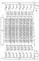
次に、図4を用いて、本実施形態における出力信号の処理を説明する。図4は、図1を参照して説明した撮像装置の構成をより詳細に示したものである。複数の画素101は、R画素、Gr画素、Gb画素、B画素を一単位とするベイヤー配列により配列されている。また、増幅回路132、コンパレータ133、メモリ134の各要素の符号には、列番号及び接続されるフォトダイオードに対応する枝番が付されている。例えば、1列目のフォトダイオード103aから出力された信号が入力される増幅回路は増幅回路132a−01aとしている。以下の説明では、特定の列の要素を指す場合に符号に枝番を付し、列を特定する必要がない場合には符号に枝番を付さないものとする。また、図4において、TG12については図示を省略している。後述の図7、図12についても同様である。
Next, processing of an output signal in the present embodiment will be described with reference to FIG. FIG. 4 shows the configuration of the imaging device described with reference to FIG. 1 in more detail. The plurality of
垂直走査回路11により走査が開始されると、まず1行目と2行目が選択される。このとき、1行目と2行目の画素101において、上述のAD変換動作が行われる。これにより、生成されたデジタル信号が各列のメモリ134に保持される。
When scanning is started by the
具体的には、1行1列目のR画素のフォトダイオード103a、103bからのデジタル信号(以降Dデータとする)はそれぞれメモリ134a−01a、134a−01bに保持される。1行2列目のGr画素のフォトダイオード103a、103bからのDデータはメモリ134a−02a、134a−02bに保持される。以下同様に1行目の各列の画素からのDデータが、対応する各列のメモリ134に保持される。
Specifically, digital signals (hereinafter referred to as D data) from the
同様に2行1列目のGb画素のフォトダイオード103a、103bからのDデータはメモリ134b−01a、134b−01bに保持される。2行2列目のB画素のフォトダイオード103a、103bからのDデータはメモリ134b−02a、134b−02bに保持される。以下同様に2行目の各列の画素からのDデータが対応する各列のメモリ134に保持される。
Similarly, D data from the
メモリ134から信号処理部17へのDデータの伝送について説明する。各メモリ134に保持されたDデータは、8列ごとのブロックに分けて扱われる。すなわち、1列目から8列目までをブロックH1、9列目から16列目までをブロックH2、…とする。各ブロックのDデータは並列に伝送される。例えば、1行目のブロックH1は、メモリ134a−01aからメモリ134a−08bに保持された16個のフォトダイオード(8個の画素)から出力されたDデータを含む。各Dデータは12ビットのデータであるため、合計192ビットのDデータが並列に伝送される。このように並列伝送することにより、高速伝送が可能となる。
Transmission of D data from the
信号処理部17aでは、入力されたDデータに基づき映像信号及び測距信号の生成処理が行われる。まず映像信号の処理について説明する。
The
まず、メモリ134a−01aとメモリ134a−01bのDデータを加算することにより、1行1列目のR画素のフォトダイオード103a、103bからのDデータを加算した加算Dデータを得る。この加算Dデータは1行1列目のR画素の映像信号として用いられる。
First, by adding the D data of the
次にメモリ134a−02aとメモリ134a−02bのDデータを加算することにより、1行2列目のGr画素のフォトダイオード103a、103bからのDデータを加算した加算Dデータを得る。この加算Dデータは1行2列目のGr画素の映像信号として用いられる。以下同様の処理により、各列の画素に対応する映像信号が得られる。
Next, by adding the D data of the
この映像信号の処理と並行して、測距信号の処理が行われる。図5は信号処理部17に設けられた測距信号の処理を行う測距信号処理部17FSの構成を示す図である。 The processing of the ranging signal is performed in parallel with the processing of the video signal. FIG. 5 is a diagram showing a configuration of a distance measurement signal processing unit 17FS provided in the signal processing unit 17 for processing a distance measurement signal.
測距信号処理部17FSは、メモリ部17ME、飽和判定部17SAT、飽和フラグ生成部17FL、加算部17AD及び信号出力部17DAを含む。メモリ部17MEは、メモリ134から入力された、フォトダイオード103aに基づくDデータ(a信号)と、フォトダイオード103bに基づくDデータ(b信号)とを一時的に保持する。飽和判定部17SATは、Dデータに基づいて信号の飽和の有無を判定する判定部である。飽和フラグ生成部17FLは、加算の対象となる4つのDデータについて、対応するフォトダイオード103a、103bの飽和判定結果の論理和を演算する。加算部17ADは、4つのフォトダイオード103a、103bからのDデータを加算し、加算Dデータを生成する。信号出力部17DAは、加算Dデータにフラグ信号を付加して測距信号処理部17FSの外部へ出力する出力部である。この信号は撮像装置の出力信号となり、撮像装置が搭載される撮像システム等のシステム処理系において焦点検出等のための測距情報として用いられる。
The ranging signal processing unit 17FS includes a memory unit 17ME, a saturation determination unit 17SAT, a saturation flag generation unit 17FL, an addition unit 17AD, and a signal output unit 17DA. The memory unit 17ME temporarily holds D data (a signal) based on the
測距信号処理部17FSは、行方向に配列された同色のフォトダイオード103a、103bからのDデータを加算して測距信号を生成する。まず、R画素の測距信号の処理を説明する。
The ranging signal processing unit 17FS adds the D data from the
飽和判定部17SATは、メモリ134a−01a、134a−03a、134a−05a、134a−07aからの各Dデータが、飽和レベルに達しているか否かを判定する。飽和判定部17SATは、飽和レベルに達していると判定した場合にはHighの信号を、飽和レベルに達していないと判定した場合にはLowの信号を飽和フラグ生成部17FLに出力する。信号が飽和レベルに達しているか否かの判定は、入力された信号が事前に設定された所定の飽和閾値よりも大きいか否かを判断することにより行うことができる。
The saturation determination unit 17SAT determines whether or not each D data from the
飽和フラグ生成部17FLは、飽和判定部17SATからの信号に基づき、4つの各Dデータの少なくとも1つが飽和閾値よりも大きい場合に、飽和フラグR_aをHighにして信号出力部17DAに出力する。すなわち、飽和フラグ生成部17FLは、飽和判定部17SATからの信号の論理和を飽和フラグR_aとして出力する。ここで、飽和閾値は、増幅回路132の出力の飽和レベル、画素101からの出力信号の飽和レベル及びAD変換レンジの飽和レベルのうち最も小さい飽和レベルに基づいて設定することができる。
The saturation flag generation unit 17FL sets the saturation flag R_a to High and outputs it to the signal output unit 17DA when at least one of the four D data is larger than the saturation threshold based on the signal from the saturation determination unit 17SAT. That is, the saturation flag generation unit 17FL outputs the logical sum of the signals from the saturation determination unit 17SAT as the saturation flag R_a. Here, the saturation threshold can be set based on the smallest saturation level among the saturation level of the output of the
同様の処理により、飽和判定部17SATは、メモリ134a−01b、134a−03b、134a−05b、134a−07bからの各Dデータを判定し、飽和フラグ生成部17FLは、飽和フラグR_bを信号出力部17DAに出力する。
By the same processing, the saturation determination unit 17SAT determines each D data from the
上述の飽和フラグR_a、R_bの生成と並行して、加算部17ADは、メモリ134a−01a、134a−03a、134a−05a、134a−07aからのDデータを加算して信号出力部17DAに出力する。これにより、1行1列目のR画素、1行3列目のR画素、1行5列目のR画素及び1行7列目のR画素の4つのフォトダイオード103aからのD信号が加算された信号が得られる。以上の処理により、1行1列目、1行3列目、1行5列目及び1行7列目の4画素分が加算されたR画素のフォトダイオード103aに基づく測距信号が得られる。このように、複数列の画素からの信号を加算して測距信号を生成することにより、撮像装置から出力される測距信号の個数を映像信号の個数よりも少なくすることができ、処理を高速化することができる。
In parallel with the generation of the saturation flags R_a and R_b, the adding unit 17AD adds the D data from the
信号出力部17DAは、4画素分加算されたR画素の測距信号の出力とともに、飽和フラグR_a、R_bを出力する。例えば、4画素分加算されたR画素の測距信号が10ビット(bit)であるとすれば、図5に示されるように、出力される信号は、この10ビットの測距信号に各1ビットの飽和フラグR_a、R_bを付与した12ビットの信号となる。このようにして、R画素の測距信号の処理が行われる。 The signal output section 17DA outputs the saturation flags R_a and R_b together with the output of the ranging signal of the R pixel added by four pixels. For example, assuming that the distance measurement signal of the R pixel added by four pixels is 10 bits, the output signal is, as shown in FIG. This is a 12-bit signal to which bit saturation flags R_a and R_b are added. Thus, the processing of the distance measurement signal of the R pixel is performed.
Gr画素の測距信号の処理も同様に行われる。すなわち、メモリ134a−02a、134a−04a、134a−06a、134a−08aからの各Dデータを判定し、飽和フラグ生成部17FLは、飽和フラグGR_aを信号出力部17DAに出力する。さらに、メモリ134a−02b、134a−04b、134a−06b、134a−08bからの各Dデータを判定し、飽和フラグ生成部17FLは、飽和フラグGR_bを信号出力部17DAに出力する。
The processing of the distance measurement signal of the Gr pixel is performed in the same manner. That is, the D data from the
上述の飽和フラグR_aの生成と並行して、加算部17ADは、メモリ134a−02a、134a−04a、134a−06a、134a−08aからのDデータを加算して信号出力部17DAに出力する。これにより、1行2列目、1行4列目、1行6列目及び1行8列目の4画素分が加算されたGr画素の測距信号が得られる。信号出力部17DAは、4画素分加算されたGr画素の測距信号の出力とともに、飽和フラグGr_a、Gr_bを出力する。
In parallel with the generation of the saturation flag R_a, the adding unit 17AD adds the D data from the
例えば、4画素分加算されたGr画素の測距信号が10ビットであるとすれば、図5に示されるように、出力される信号は、この10ビットの測距信号に各1ビットの飽和フラグGr_a、Gr_bを付与した12ビットの信号となる。このようにして、Gr画素の測距信号の処理が行われる。 For example, assuming that the distance measurement signal of the Gr pixel added by four pixels is 10 bits, as shown in FIG. 5, the output signal is obtained by adding a 1-bit saturation signal to the 10-bit distance measurement signal. This is a 12-bit signal to which flags Gr_a and Gr_b are added. Thus, the processing of the ranging signal of the Gr pixel is performed.
信号処理部17bでも同様な処理が行われ、2行1列目のGb画素の映像信号、2行2列目のB画素の映像信号、2行3列目のGb画素の映像信号、2行4列目のB画素の映像信号、…を出力する。
The same processing is performed in the
それとともに、4画素分加算されたGb画素の測距信号に飽和フラグGb_a及び飽和フラグGb_bが付与された信号と、4画素分加算されたB画素の測距信号に飽和フラグB_a及び飽和フラグB_bが付与された信号とが出力される。 At the same time, a signal obtained by adding the saturation flag Gb_a and the saturation flag Gb_b to the distance measurement signal of the Gb pixel added by four pixels, and a saturation flag B_a and a saturation flag B_b by the distance measurement signal of the B pixel added by four pixels Is output.
上述のように、撮像装置からの出力信号は、各画素101からの映像信号(フォトダイオード103a、103bからの信号を加算した信号)と、4画素分加算された測距信号(フォトダイオード103aからの信号)の2種である。すなわち、フォトダイオード103bからの信号自体は出力されない。なぜなら、フォトダイオード103a、103bからの信号を加算した信号と、フォトダイオード103aからの信号が出力されているので、その差分により、フォトダイオード103bからの信号を演算で求めることができるためである。
As described above, the output signal from the imaging device includes a video signal from each pixel 101 (a signal obtained by adding the signals from the
この演算は例えば以下のように行うことができる。フォトダイオード103a、103bからのDデータを加算した信号を4画素分加算する。次に、その値から4画素分加算されたフォトダイオード103aからのDデータを減算する。この処理により、4画素加算されたフォトダイオード103bからのDデータを求めることができる。
This calculation can be performed, for example, as follows. A signal obtained by adding the D data from the
このように、フォトダイオード103bからのDデータは出力されない。しかしながら、上述の説明のようにフォトダイオード103bの飽和判定を行い、フォトダイオード103bの飽和フラグを出力することがより好適である。その理由は、以下のとおりである。
Thus, the D data from the
フォトダイオード103aから出力される信号レベルがフォトダイオード103bから出力される信号レベルよりも非常に小さい場合を考える。例えば、フォトダイオード103aの信号レベルが80であり、フォトダイオード103bの信号レベルが350であり、AD変換における回路飽和レベルが256であるものとする。
Consider a case where the signal level output from the
このとき、フォトダイオード103aからの信号をAD変換した値は80になり、フォトダイオード103bからの信号をAD変換した値は256となり、これらの合計値は336となる。
At this time, the value obtained by AD-converting the signal from the
各画素のフォトダイオード103aに対応する信号と、各画素のフォトダイオード103a、103bの加算信号とをいずれも画素間で加算せずに個別に出力している場合、すなわち、測距信号と映像信号がいずれも画素間で加算されていない場合を考える。この場合は、後段でこれらの差分を計算すれば、フォトダイオード103bに対応する信号のレベルが256であることが算出でき、この値に基づき回路飽和が生じているか否かを判定できる。
When a signal corresponding to the
しかしながら、本実施形態では、フォトダイオード103aの信号は4画素分加算されているため、各画素のフォトダイオード103aの信号レベルを後段で個別に算出することができない。そのため、上述の差分を行ったとしても各画素のフォトダイオード103bについて回路飽和が生じているか否かを判別するということができない場合がある。
However, in the present embodiment, since the signal of the
さらに、フォトダイオード103a、103bの加算信号、4画素加算されたフォトダイオード103aの出力信号及びこれに対応する飽和フラグのいずれを参照しても、フォトダイオード103bの信号が飽和しているか否かが判定できない場合もある。そのため、フォトダイオード103bの信号の飽和を判定するために、フォトダイオード103bの飽和レベルに達しているか否かを示す飽和フラグを出力することが好ましい。
Further, whether the signal of the
以上のように、本実施形態では撮像装置が測距信号を加算して出力する場合に、出力信号に飽和フラグを含ませている。これにより、加算後の出力信号に飽和レベルに達した信号が含まれているか否かを外部のシステム処理系に伝えることが可能となる。 As described above, in the present embodiment, when the imaging apparatus adds and outputs the distance measurement signal, the output signal includes the saturation flag. As a result, it is possible to inform an external system processing system whether or not the output signal after addition includes a signal that has reached the saturation level.
これにより、飽和により誤った値となった加算Dデータにより、システム処理系が誤った測距情報を得ることによる誤認識が生じるおそれを低減することができる。システム処理系は、飽和フラグが信号の飽和を示す測距信号を焦点検出のための測距動作に用いないようにする。この場合には、システム処理系は、飽和フラグが信号の飽和を示す測距信号に代えて隣接する画素の信号からの補間で得た信号を用いても良い。あるいは、システム処理系は、当該測距信号がないものとして処理しても良い。 As a result, it is possible to reduce a possibility that the system processing system may obtain erroneous distance measurement information to cause erroneous recognition due to the added D data having an erroneous value due to saturation. The system processing system does not use the ranging signal indicating that the saturation flag indicates the saturation of the signal in the ranging operation for focus detection. In this case, the system processing system may use a signal obtained by interpolation from a signal of an adjacent pixel instead of the ranging signal indicating that the saturation flag indicates signal saturation. Alternatively, the system processing system may perform processing assuming that there is no ranging signal.
なお、上述の説明では、飽和フラグR_a、R_b、Gr_a、Gr_bをそれぞれ個別に出力しているため、これらは合計4ビットのデータとなっている。しかしながら、飽和フラグR_a、R_b、Gr_a、Gr_bの一部又は全部の論理和を算出して3ビット以下に圧縮してもよく、例えば1ビットに圧縮して出力してもよい。飽和フラグを圧縮してビット数を低減することにより、Dデータの伝送負荷を低減できる。 In the above description, since the saturation flags R_a, R_b, Gr_a, and Gr_b are individually output, these are 4-bit data in total. However, the logical sum of a part or all of the saturation flags R_a, R_b, Gr_a, and Gr_b may be calculated and compressed to 3 bits or less, or may be compressed to 1 bit and output. By compressing the saturation flag and reducing the number of bits, the transmission load of D data can be reduced.
また、上述の説明では、信号出力部17DAが、加算した測距信号に飽和フラグを付加して出力する例が示されているが、映像信号に飽和フラグを付加して出力してもよい。 Further, in the above description, an example is shown in which the signal output unit 17DA adds a saturation flag to the added distance measurement signal and outputs the added signal, but the signal output unit 17DA may add a saturation flag to the video signal and output the signal.
さらに、上述の説明では、1つの画素101に2つの光電変換部を有する構成を例示して説明しているが、1つの画素101が2より多い複数の光電変換部を有する構成であってもよい。具体的には以下のとおりである。
Further, in the above description, a configuration in which one
画素部10に含まれる複数の画素101が有する光電変換部の個数をm個(mは2以上の整数)とする。このとき、測距信号(第1の信号)はm個よりも少ないn個(nは整数)の光電変換部の信号電荷に基づいて生成することができる。このとき、上述の測距信号とともに用いられるもう一つの測距信号(第3の信号)は、上述のm個の光電変換部から上述のn個の光電変換部を除いた(m−n)個の光電変換部の信号電荷に基づくものとなる。本実施形態のフォトダイオード103a、103bからなる2個の光電変換部を有する構成はm=2、n=1とした場合の例であるが、m、nがこれ以外の値であってもよく、同様の効果が得られる。
The number of photoelectric conversion units included in the plurality of
また、上述の説明では、メモリ134からは8画素からのDデータを並行的に伝送する構成を例示しているが、この画素数は8画素より少なくても多くてもよい。さらに測距信号は4画素からのDデータの加算により生成される構成を例示しているが、この画素数も4画素より少なくても多くてもよい。
Further, in the above description, the configuration in which the D data from eight pixels are transmitted in parallel from the
また、複数の画素101のフォトダイオード103aからの信号同士の加算処理及びフォトダイオード103aの信号レベルが飽和レベルに達しているか否かの判定処理は、撮像装置の外部に設けられたシステム処理系が行うようにしてもよい。すなわち、信号処理部17a、17bの一部又は全部の機能は、撮像装置ではなく、システム処理系に設けられていてもよい。
Further, the processing of adding the signals from the
なお、測距信号は、画素部10のすべての画素101から出力させる必要はなく、測距に必要な個数だけあればよい。すなわち、測距信号の個数は映像信号(第2の信号)の個数よりも少なくてもよい。例えば、測距信号は、画素部10の一部の領域のみから出力させ、映像信号は画素部10の全領域から出力させるようにしてもよい。このようにすることで、信号処理を高速化することができる。
Note that the distance measurement signals do not need to be output from all the
(第2の実施形態)
図4及び図6を用いて、第2の実施形態に係る撮像装置における出力信号の処理を説明する。第2の実施形態に係る撮像装置の構成は測距信号処理部17FSを除き第1の実施形態と同様であるため、重複する説明は省略又は簡略化する。
(Second embodiment)
Processing of an output signal in the imaging device according to the second embodiment will be described with reference to FIGS. The configuration of the imaging apparatus according to the second embodiment is the same as that of the first embodiment except for the distance measurement signal processing unit 17FS, and therefore, duplicate description will be omitted or simplified.
第2の実施形態において、測距信号処理部17FSは、第1の実施形態とは異なり、隣接した画素、すなわち異なる色のカラーフィルタを有するフォトダイオードからのDデータ同士の加算を行う。 In the second embodiment, unlike the first embodiment, the ranging signal processing unit 17FS performs addition of D data from adjacent pixels, that is, photodiodes having color filters of different colors.
飽和判定部17SATは、メモリ134a−01a、134a−01b、134a−03a、134a−03bからの各R画素に対応するDデータが、飽和レベルに達しているか否かを判定する。飽和判定部17SATは、飽和レベルに達していると判定した場合にはHighの信号を、飽和レベルに達していないと判定した場合にはLowの信号を飽和フラグ生成部17FLに出力する。飽和フラグ生成部17FLは、飽和判定部17SATからの信号に基づき、4つの各Dデータの少なくとも1つが飽和閾値よりも大きい場合に、飽和フラグRをHighにして信号出力部17DAに出力する。
The saturation determination unit 17SAT determines whether the D data corresponding to each R pixel from the
さらに、飽和判定部17SATは、メモリ134a−02a、134a−02b、134a−04a、134a−04bからの各Gr画素のDデータが、飽和レベルに達しているか否かを判定する。飽和判定部17SATは、飽和レベルに達していると判定した場合にはHighの信号を、飽和レベルに達していないと判定した場合にはLowの信号を飽和フラグ生成部17FLに出力する。飽和フラグ生成部17FLは、飽和判定部17SATからの信号に基づき、4つの各Dデータの少なくとも1つが飽和閾値よりも大きい場合に、飽和フラグGrをHighにして信号出力部17DAに出力する。
Further, the saturation determination unit 17SAT determines whether or not the D data of each Gr pixel from the
加算部17ADは、メモリ134a−01a、134a−02a、134a−03a、134a−04aからのD信号を加算して信号出力部17DAに出力する。これにより、1行1列目〜1行4列目の4つのフォトダイオード103aの信号を加算した出力が得られる。この信号は、測距信号として用いられる。
The addition unit 17AD adds the D signals from the
信号出力部17DAは、4画素分加算された測距信号の出力とともに、飽和フラグRと飽和フラグGrを出力する。 The signal output unit 17DA outputs the saturation flag R and the saturation flag Gr together with the output of the distance measurement signal added for four pixels.
例えば、4画素分加算された測距信号が10ビットであるとすれば、図6に示されるように、出力される信号は、この10ビットの測距信号に各1ビットの飽和フラグR、Grを付与した12ビットの信号となる。このようにして、測距信号の処理が行われる。 For example, assuming that the distance measurement signal added for four pixels has 10 bits, as shown in FIG. 6, the output signal is obtained by adding a 1-bit saturation flag R, It becomes a 12-bit signal to which Gr has been added. In this way, the processing of the ranging signal is performed.
例えば、4画素分加算されたR画素の測距信号が10ビット(bit)であるとすれば、図5に示されるように、出力される信号は、この10ビットの測距信号に各1ビットの飽和フラグR、Grを付与した12ビットの信号となる。このようにして、R画素の測距信号の処理が行われる。 For example, assuming that the distance measurement signal of the R pixel added by four pixels is 10 bits, the output signal is, as shown in FIG. This is a 12-bit signal to which bit saturation flags R and Gr are added. Thus, the processing of the distance measurement signal of the R pixel is performed.
信号処理部17bにおいて同様な処理が行われ、2行1列目〜2行4列目の4画素分加算された測距信号に飽和フラグGb、Bが付与された信号が出力される。
Similar processing is performed in the
以上のように、第2実施形態では、第1実施形態と同様に測距信号に飽和フラグを付与した信号の出力が可能であり、同様の効果が得られる。これとともに、測距信号の空間的サンプリング位相の解像度が高いので、測距精度が向上し得る。なお、上述の説明では、飽和フラグRと飽和フラグGrをそれぞれ個別に出力しているが、飽和フラグRと飽和フラグGrの論理和を算出することで、1ビットに圧縮して出力してもよい。飽和フラグを圧縮してビット数を低減することにより、Dデータの伝送負荷を低減できる。 As described above, in the second embodiment, it is possible to output a signal in which the saturation flag is added to the ranging signal as in the first embodiment, and the same effect is obtained. At the same time, the resolution of the spatial sampling phase of the ranging signal is high, so that the ranging accuracy can be improved. In the above description, the saturation flag R and the saturation flag Gr are individually output. However, by calculating the logical sum of the saturation flag R and the saturation flag Gr, the saturation flag R and the saturation flag Gr can be compressed and output to 1 bit. Good. By compressing the saturation flag and reducing the number of bits, the transmission load of D data can be reduced.
(第3の実施形態)
図7から図9を参照して第3の実施形態を説明する。本実施形態は、画素から出力された信号をデジタル信号に変換せず、アナログ信号のまま出力する回路構成を有する撮像装置に関するものである。
(Third embodiment)
A third embodiment will be described with reference to FIGS. The present embodiment relates to an imaging apparatus having a circuit configuration that does not convert a signal output from a pixel into a digital signal and outputs the signal as an analog signal.
図7は、第3の実施形態における撮像装置の構成を示す図である。本実施形態の撮像装置は第1及び第2の実施形態のように列ごとにAD変換を行う回路を有していないため、コンパレータ133及びメモリ134が設けられていない。一方、本実施形態の撮像装置には、加算スイッチ135(加算部)及び飽和判定部136が列ごとに設けられている。以下、本実施形態の撮像装置の構成について第1及び第2の実施形態と異なる部分を中心に説明する。
FIG. 7 is a diagram illustrating a configuration of an imaging device according to the third embodiment. The imaging device of the present embodiment does not include a circuit for performing AD conversion for each column unlike the first and second embodiments, and thus does not include the
加算スイッチ135は、隣接する列の増幅回路132同士の間に設けられている。すなわち、例えば、1列目の増幅回路132a−01と2列目の増幅回路132a−02の間には、加算スイッチ135a−01が設けられている。加算スイッチ135がオンになると、隣接する列の間の信号が加算される。
The
増幅回路132には、飽和判定部136が接続されている。飽和判定部136は、増幅回路132で増幅された信号の飽和を判定し、判定結果を示す飽和フラグを出力する。水平走査回路16aは、各列の増幅回路132からの出力信号と飽和判定部136からの飽和フラグとを順次出力アンプ18aに出力させる。水平走査回路16bは、各列の増幅回路132からの出力信号と飽和判定部136からの飽和フラグとを順次出力アンプ18bに出力させる。
The saturation determination section 136 is connected to the
図8は、増幅回路132内部の回路、加算スイッチ135及び飽和判定部136をより詳細に示す図である。図8では、各列の増幅回路132、加算スイッチ135及び飽和判定部136のうち、読み出し回路13a側の1列目から4列目までを抜き出して例示している。
FIG. 8 is a diagram illustrating the circuit inside the
増幅回路132は、増幅器141、スイッチ142、サンプルホールド容量143を含む。画素101からの信号は増幅回路132の入力端子に入力される。この入力端子を増幅回路132の入力端子IN01、IN02、…とする。増幅回路132の出力端子は飽和判定部136及びスイッチ142の一端に接続される。スイッチ142の他端はサンプルホールド容量143の一端及び加算スイッチ135の一端に接続される。この接続ノードは、増幅回路132の出力端子OUT1、OUT2、…である。加算スイッチ135の他端は、隣接する列の出力端子OUT1、OUT2、…のノードに接続される。サンプルホールド容量143の他端は接地される。飽和判定部136から飽和フラグを出力する端子は出力端子J01、J02、…とする。
The
スイッチ142及びサンプルホールド容量143はサンプルホールド回路として動作する。スイッチ142を制御する制御信号amp_shがHighになると、スイッチ142がオンになり、増幅器141の出力電圧がサンプルホールド容量143にサンプリングされる。制御信号amp_shがLowになるとスイッチ142がオフになり、増幅器141の出力電圧がサンプルホールド容量143にホールドされる。 The switch 142 and the sample and hold capacitor 143 operate as a sample and hold circuit. When the control signal amp_sh for controlling the switch 142 becomes High, the switch 142 is turned on, and the output voltage of the amplifier 141 is sampled by the sample-and-hold capacitor 143. When the control signal amp_sh becomes Low, the switch 142 is turned off, and the output voltage of the amplifier 141 is held by the sample hold capacitor 143.
加算を行わず、列ごとに独立に信号を出力する場合には、すべての加算スイッチ(135a−01、135a−02、135a−03、135a−04、…)をオフ状態にする。これにより、IN01、IN02、…に入力された信号に応じた電圧がOUT01、OUT02、…にそれぞれ現れる。 When signals are output independently for each column without performing addition, all addition switches (135a-01, 135a-02, 135a-03, 135a-04, ...) are turned off. As a result, voltages corresponding to the signals input to IN01, IN02,... Appear at OUT01, OUT02,.
4列分の信号を加算平均して出力する場合には、制御信号amp_shがLowになり出力がホールドされている状態で、加算スイッチ135a−01、135a−02、135a−03をオン状態にし、135−04をオフ状態にする。このようにすることで、OUT1端子、OUT2端子、OUT3端子、OUT4端子の出力電圧が加算平均される。この場合、飽和判定部136は、加算平均する前の信号に対して、増幅回路132の出力が飽和レベルに達しているか否かを判定することができる。
When the signals of four columns are added and averaged and output, the addition switches 135a-01, 135a-02 and 135a-03 are turned on while the control signal amp_sh is Low and the output is held, Turn 135-04 off. In this manner, the output voltages of the OUT1, OUT2, OUT3, and OUT4 terminals are added and averaged. In this case, the saturation determination unit 136 can determine whether the output of the
水平走査回路16aは、各列のサンプルホールド容量143と、飽和判定部136の出力信号を順次走査して、出力アンプ18aへ伝送する。
The
図9(a)は、本実施形態に係る画素101内部の等価回路を示す図である。本実施形態の画素101が第1の実施形態の画素101と異なる点は、画素回路110が1つのみである点である。画素回路110は、転送トランジスタ104a、104bの2つの転送トランジスタを含む。フォトダイオード103a、103bは、それぞれ転送トランジスタ104a、104bを介して同一の出力トランジスタ106のゲートに接続されている。転送トランジスタ104a、104bは、それぞれ垂直走査回路11から独立に送信される制御信号Tx_a、Tx_bにより制御される。その他の点は第1の実施形態と同様であるため説明を省略する。
FIG. 9A is a diagram illustrating an equivalent circuit inside the
図9(b)は、画素回路110の駆動方法を示す一画素行の駆動タイミングチャートである。図2(b)に示した第1の実施形態と異なる動作について説明する。
FIG. 9B is a driving timing chart of one pixel row illustrating a driving method of the
時刻T2までの動作は第1の実施形態とほぼ同様である。時刻T7において、制御信号Tx_aがHighになり、転送トランジスタ104aがオンになる。この動作により、フォトダイオード103aに蓄積された信号電荷が出力トランジスタ106aのゲートに転送される。その後、時刻T8において、制御信号Tx_aがLowになり、転送トランジスタ104aがオフになる。この動作が終了した時刻Taにおいて、フォトダイオード103aで生成された信号電荷量に応じた電圧振幅が垂直出力線102に現れる。
The operation until time T2 is almost the same as in the first embodiment. At time T7, the control signal Tx_a becomes High, and the
続いて時刻T9において、制御信号Tx_bがHighになり、転送トランジスタ104bがオンになる。この動作により、フォトダイオード103bに蓄積された信号電荷も出力トランジスタ106bのゲートに転送される。その後、時刻T10において、制御信号Tx_bがLowになり、転送トランジスタ104bがオフになる。この動作が終了した時刻(Ta+b)において、フォトダイオード103aで生成された信号電荷量とフォトダイオード103bで生成された信号電荷量との和に応じた電圧振幅が垂直出力線102に現れる。その後の時刻T5、T6の動作は第1の実施形態とほぼ同様である。
Subsequently, at time T9, the control signal Tx_b becomes High, and the
図10(a)は本実施形態に係る画素101の上面模式図である。本実施形態の画素101は画素回路110が2つのフォトダイオード103a、103bに対して共通に設けられている点で第1の実施形態と異なる。
FIG. 10A is a schematic top view of the
このような画素の構造とすることで、時刻Taにおいて垂直出力線102の信号を読み出すことで、フォトダイオード103a単独の信号を読み出すことができる。この信号は測距信号として使用することができる。また、時刻(Ta+b)において垂直出力線102の信号を読み出すことで、受光部全体の信号を読み出すことができる。この信号は映像信号として使用することができる。
With such a pixel structure, a signal of the
図10(b)は、図10(a)でα−β線で示した部分の断面図である。α−β線の部分の断面構造は図3(a)と同様であるため説明を省略する。 FIG. 10B is a cross-sectional view of a portion indicated by line α-β in FIG. The cross-sectional structure of the portion along the line α-β is the same as that shown in FIG.
第3の実施形態では、測距信号を増幅回路132の出力端子部分で加算して加算信号を出力するとともに、飽和フラグを出力する。この構成により、本実施形態では、第1及び第2の実施形態とは異なり、加算及び飽和の判定がデジタル信号ではなくアナログ信号の状態で行われる。撮像装置外部のシステム処理系は、この飽和フラグを参照して加算信号に飽和レベルに達した信号が含まれているか否かを判断することができる。したがって、第1の実施形態と同様の効果が得られる。これに加え、本実施形態では読み出し回路13a、13bで加算して得た加算信号を出力するため、信号の個数が少なくすることができ、伝送時間を短縮できる。これにより、処理をより高速化することができる。
In the third embodiment, the ranging signal is added at the output terminal of the
(第4の実施形態)
図11は、第4の実施形態に係る撮像装置の構成を示す図である。本実施形態における画素101の構成は、第3の実施形態として説明した図9(a)、図10に示されている構成と同様である。また、本実施形態の撮像装置のその他の要素の構成はメモリを除き第1の実施形態と同様である。本実施形態では第1の実施形態のメモリ134に代えて、測距信号メモリ1341及び映像信号メモリ1342が設けられている。
(Fourth embodiment)
FIG. 11 is a diagram illustrating a configuration of an imaging device according to the fourth embodiment. The configuration of the
測距信号メモリ1341及び映像信号メモリ1342の動作について説明する。図9(b)における時刻Taのタイミングで、コンパレータ133においてフォトダイオード103aからの信号のAD変換が行われる(以降、a変換と表記する)。このa変換により生成されたデジタル信号(a信号)は、測距信号メモリ1341に保持される。
The operation of the ranging
続いて、図9(b)における時刻(Ta+b)のタイミングで、コンパレータ133において、フォトダイオード103a及びフォトダイオード103bからの信号の和に相当する信号のAD変換が行われる(以降、a+b変換と表記する)。このa+b変換により生成されたデジタル信号(a+b信号)は、映像信号メモリ1342に保持される。
Subsequently, at the timing of time (Ta + b) in FIG. 9B, the
すなわち、本実施形態では、画素101が測距信号と映像信号を出力可能な構成となっていることに対応して、測距信号と映像信号を別々に保持できるように測距信号メモリ1341及び映像信号メモリ1342が設けられている。
That is, in the present embodiment, corresponding to the configuration in which the
次に、図12と図13を参照しつつ、本実施形態における出力信号の処理を第1乃至第3の実施形態と異なる部分を中心に説明する。信号処理部17aでは、入力されたDデータに基づき映像信号及び測距信号の生成処理が行われる。まず映像信号の処理について説明する。
Next, with reference to FIGS. 12 and 13, the processing of the output signal in the present embodiment will be described focusing on the differences from the first to third embodiments. The
まず、映像信号メモリ1342a−01のデータから、1行1列目のR画素のフォトダイオード103a、103bからの信号の和に相当するDデータを得る。このDデータは1行1列目のR画素の映像信号として用いられる。
First, D data corresponding to the sum of signals from the
次に映像信号メモリ1342a−02のデータから、1行2列目のGr画素のフォトダイオード103a、103bからの信号の和に相当するDデータを得る。このDデータは1行2列目のGr画素の映像信号として用いられる。以下同様の処理により、各列の画素に対応する映像信号が得られる。
Next, D data corresponding to the sum of signals from the
この映像信号の処理と並行して、測距信号の処理が行われる。図13は信号処理部17に設けられた測距信号の処理を行う測距信号処理部17FSの構成を示す図である。 The processing of the ranging signal is performed in parallel with the processing of the video signal. FIG. 13 is a diagram showing a configuration of a ranging signal processing unit 17FS provided in the signal processing unit 17 and processing a ranging signal.
飽和判定部17SATは、測距信号メモリ1341a−01、1341a−02、1341a−03、1341a−04からの各Dデータが、飽和レベルに達しているか否かを判定する。飽和判定部17SATは、飽和レベルに達していると判定した場合にはHighの信号を、飽和レベルに達していないと判定した場合にはLowの信号を飽和フラグ生成部17FLに出力する。
The saturation determination unit 17SAT determines whether each D data from the ranging
飽和フラグ生成部17FLは、飽和判定部17SATからの信号に基づき、4つの各Dデータの少なくとも1つが飽和閾値よりも大きい場合に、飽和フラグAをHighにして信号出力部17DAに出力する。すなわち、飽和フラグ生成部17FLは、飽和判定部17SATからの信号の論理和を飽和フラグAとして出力する。 The saturation flag generation unit 17FL sets the saturation flag A to High and outputs it to the signal output unit 17DA when at least one of the four D data is larger than the saturation threshold based on the signal from the saturation determination unit 17SAT. That is, the saturation flag generation unit 17FL outputs the logical sum of the signals from the saturation determination unit 17SAT as the saturation flag A.
飽和判定部17SATは、さらに、映像信号メモリ1342a−01からのDデータと、測距信号メモリ1341a−01からのDデータとの差分に相当する信号(b信号)を生成する。飽和判定部17SATは、差分に相当する信号に対し信号飽和レベルに達しているか否かを判定する。映像信号メモリ1342a−02からのDデータと、測距信号メモリ1341a−02からのDデータとの差分についても同様に判定が行われる。さらに、映像信号メモリ1342a−03からのDデータと、測距信号メモリ1341a−03からのDデータとの差分、映像信号メモリ1342a−04からのDデータと、測距信号メモリ1341a−04からのDデータとの差分についても判定が行われる。以上のようにして4つの差分が演算される。
The saturation determination unit 17SAT further generates a signal (b signal) corresponding to the difference between the D data from the
飽和フラグ生成部17FLは、飽和判定部17SATからの信号に基づき、これらの4つの差分の少なくとも1つが飽和閾値よりも大きい場合に、飽和フラグBをHighにして信号出力部17DAに出力する。 When at least one of these four differences is larger than the saturation threshold based on the signal from the saturation determination unit 17SAT, the saturation flag generation unit 17FL sets the saturation flag B to High and outputs it to the signal output unit 17DA.
上述の飽和フラグA、Bの生成と並行して、加算部17ADは、測距信号メモリ1341a−01、1341a−02、1341a−03、1341a−04からのDデータを加算して信号出力部17DAに出力する。これにより、1行1列目〜1行4列目の4つのフォトダイオード103aの信号を加算した出力が得られる。この信号は、測距信号として用いられる。
In parallel with the generation of the saturation flags A and B, the addition unit 17AD adds the D data from the distance
信号出力部17DAは、4画素分加算された測距信号の出力とともに、飽和フラグAと飽和フラグBを出力する。例えば、4画素分加算された測距信号が10ビットであるとすれば、図13に示されるように、出力される信号は、この10ビットの測距信号に各1ビットの飽和フラグA、Bを付与した12ビットの信号となる。このようにして、測距信号の処理が行われる。信号処理部17bにおいて同様な処理が行われ、2行1列目〜2行4列目の4画素分加算された測距信号に飽和フラグGb、Bが付与された信号が出力される。
The signal output unit 17DA outputs the saturation flag A and the saturation flag B together with the output of the distance measurement signal added for four pixels. For example, if the distance measurement signal added for four pixels is 10 bits, as shown in FIG. 13, the output signal is obtained by adding a 1-bit saturation flag A, This is a 12-bit signal to which B has been added. In this way, the processing of the ranging signal is performed. Similar processing is performed in the
本実施形態においても、第1の実施形態と同様の効果を得ることができる。なお、上述の説明では、飽和フラグAと飽和フラグBをそれぞれ個別に出力しているが、飽和フラグAと飽和フラグBの論理和を算出することで、1ビットに圧縮して出力してもよい。飽和フラグを圧縮してビット数を低減することにより、Dデータの伝送負荷を低減できる。 Also in the present embodiment, the same effect as in the first embodiment can be obtained. In the above description, the saturation flag A and the saturation flag B are individually output. Good. By compressing the saturation flag and reducing the number of bits, the transmission load of D data can be reduced.
(第5の実施形態)
本実施形態は、第1乃至第4の実施形態で述べた撮像装置を適用した撮像システムに関する。
(Fifth embodiment)
This embodiment relates to an imaging system to which the imaging device described in the first to fourth embodiments is applied.
撮像システムの一例として、デジタルスチルカメラ、デジタルカムコーダー、監視カメラなどがあげられる。図14に、撮像システムの例としてデジタルスチルカメラに撮像装置を適用した場合の模式図を示す。 Examples of an imaging system include a digital still camera, a digital camcorder, and a surveillance camera. FIG. 14 is a schematic diagram illustrating a case where an imaging apparatus is applied to a digital still camera as an example of an imaging system.
図14に例示した撮像システムは、レンズの保護のためのバリア151、被写体の光学像を撮像装置154に結像させるレンズ152、レンズ152を通過する光量を可変にするための絞り153を有する。レンズ152、絞り153は撮像装置154に光を集光する光学系である。また、図14に例示した撮像システムは、撮像装置154より出力される出力信号の処理を行う出力信号処理部155を有する。出力信号処理部155は必要に応じて各種の補正、圧縮を行って信号を出力する動作を行う。
The imaging system illustrated in FIG. 14 includes a
図14に例示した撮像システムはさらに、画像データを一時的に記憶するためのバッファメモリ部156、外部コンピュータ等と通信するための外部インターフェース部157を有する。さらに撮像システムは、撮像データの記録又は読み出しを行うための半導体メモリ等の着脱可能な記録媒体159、記録媒体159に記録又は読み出しを行うための記録媒体制御インターフェース部158を有する。さらに撮像システムは、各種演算とデジタルスチルカメラ全体を制御する全体制御・演算部1510、撮像装置154と出力信号処理部155に各種タイミング信号を出力するタイミング発生部1511を有する。ここで、タイミング信号などは外部から入力されてもよく、撮像システムは少なくとも撮像装置154と、撮像装置154から出力された出力信号を処理する出力信号処理部155とを有すればよい。
The imaging system illustrated in FIG. 14 further includes a
出力信号処理部155は、第1乃至第4の実施形態で述べたシステム処理系とすることができる。すなわち、出力信号処理部155は、デジタルA+B信号(2つのフォトダイオード103a、103bからの信号の和に相当する信号)からデジタルA信号(フォトダイオード103aからの信号)を差し引く。これにより、デジタルB信号(フォトダイオード103bからの信号)が生成される。そして、出力信号処理部155は、デジタルA信号とデジタルB信号とを用いて、位相差検出方式の焦点検出を行う。また、出力信号処理部155はデジタルA+B信号を用いて画像の形成を行う。なお、第1乃至第4の実施形態で述べた読み出し回路13a、13bで行われる処理の一部又は全部を出力信号処理部155で行うように構成してもよい。
The output
以上のように、本実施形態の撮像システムは、撮像装置154を適用して焦点検出動作及び撮像動作を行うことが可能である。
As described above, the imaging system of the present embodiment can perform the focus detection operation and the imaging operation by applying the
(その他の実施形態)
本発明は、上述の実施形態の1以上の機能を実現するプログラムを、ネットワーク又は記録媒体を介してシステム又は装置に供給し、そのシステム又は装置のコンピュータにおける1以上のプロセッサがプログラムを読み出し実行する処理でも実現可能である。また、1以上の機能を実現する回路(例えば、ASIC)によっても実現可能である。
(Other embodiments)
The present invention supplies a program realizing one or more functions of the above-described embodiments to a system or an apparatus via a network or a recording medium, and one or more processors in a computer of the system or the apparatus read and execute the program. Processing can also be realized. Further, it can also be realized by a circuit (for example, an ASIC) that realizes one or more functions.
なお、上記実施形態は、いずれも本発明を実施するにあたっての具体化の例を示したものに過ぎず、これらによって本発明の技術的範囲が限定的に解釈されてはならないものである。すなわち、本発明はその技術思想、又はその主要な特徴から逸脱することなく、様々な形で実施することができる。また、これまで述べた各実施形態を種々組み合わせて実施することができる。 It should be noted that each of the above-described embodiments is merely an example of a concrete example for carrying out the present invention, and the technical scope of the present invention should not be interpreted in a limited manner. That is, the present invention can be implemented in various forms without departing from the technical idea or the main features. Also, the embodiments described above can be implemented in various combinations.
10 画素部
101 画素
103 フォトダイオード(光電変換部)
17FL 飽和フラグ生成部
17SAT 飽和判定部
17AD 加算部
17DA 出力部
10
17FL Saturation flag generation unit 17SAT Saturation determination unit 17AD Addition unit 17DA Output unit
Claims (13)
前記複数のマイクロレンズの各々は、前記複数の画素のうちの互いに異なる1つの画素と対応して配されており、
前記複数の画素の各々が、信号電荷を生成するm個(mは2以上の整数)の光電変換部を含むとともに、前記信号電荷に基づいた信号を出力し、
前記複数の画素の少なくとも一部の前記画素の各々が、前記m個の光電変換部のうち、前記m個よりも少ないn個(nは整数)の前記光電変換部の前記信号電荷に基づいた第1の信号を出力する
画素部と、
互いに異なる複数の前記画素から出力された複数の前記第1の信号同士を加算する加算部と、
前記複数の第1の信号の各々と所定の閾値との比較によって複数の判定結果を生成し、前記複数の判定結果を用いて、前記加算部により加算される前記複数の第1の信号が前記所定の閾値より大きい信号を含むか否かを示すフラグ信号を生成する判定部と、
前記フラグ信号及び前記加算部で前記複数の第1の信号同士を加算して得られた信号を出力する出力部と
を有することを特徴とする撮像装置。 A pixel portion having a plurality of pixels and a plurality of microlenses arranged in a matrix,
Each of the plurality of microlenses is arranged corresponding to one different pixel among the plurality of pixels,
Each of the plurality of pixels includes m (m is an integer of 2 or more) photoelectric conversion units that generate signal charges, and outputs a signal based on the signal charges;
Each of at least a portion of said pixels of said plurality of pixels, among the m photoelectric conversion unit, less the n than the m (n is an integer) based on the signal charges of the photoelectric conversion unit of A pixel unit for outputting the first signal,
An adding unit that adds the plurality of first signals output from the plurality of pixels different from each other,
It generates a comparison to result plurality of determination results of each and Jo Tokoro threshold value of the plurality of first signals, using the plurality of determination results, a first of said plurality to be added by the addition unit A determining unit that generates a flag signal indicating whether the signal includes a signal greater than the predetermined threshold ,
Imaging device and having an output section for outputting a signal obtained by adding the first signal among the plurality in the flag signal and the addition unit.
前記出力部から出力される、前記m個の光電変換部の前記信号電荷に基づいた第2の信号に基づく信号の個数よりも少ない
ことを特徴とする請求項1に記載の撮像装置。 The number of signals output from the output unit based on the first signal is
The imaging apparatus according to claim 1, wherein the number of signals output from the output unit and based on the second signal based on the signal charges of the m photoelectric conversion units is smaller than the number of signals.
ことを特徴とする請求項1乃至3のいずれか1項に記載の撮像装置。 The determination unit, among the m photoelectric conversion unit, a third signal based on the n excluding the photoelectric conversion section (m-n) pieces of said signal charges of said photoelectric conversion unit, a plurality of said third signal corresponding to a plurality of pixels for outputting a first signal of the plurality of the the addition is performed, further characterized in that determining whether to include a larger signal than the predetermined threshold The imaging device according to claim 1.
前記複数の画素の少なくとも一部の前記画素の各々は、
前記n個の光電変換部の前記信号電荷に基づいた前記第1の信号をアナログ信号として出力し、
前記m個の光電変換部のうち、前記n個の光電変換部を除いた(m−n)個の前記光電変換部の前記信号電荷に基づいた第3の信号をアナログ信号として出力し、
前記複数のアナログデジタル変換回路の各々は、
前記第1の信号を前記第1の信号に基づくデジタル信号に変換し、
前記第3の信号を前記第3の信号に基づくデジタル信号に変換し、
前記加算部は、
前記複数の画素のうちの第1の画素の前記第1の信号に基づくデジタル信号と、前記第1の画素の前記第3の信号に基づくデジタル信号とを加算し、
前記第1の画素の前記第1の信号に基づくデジタル信号と、前記複数の画素のうちの前記第1の画素とは異なる第2の画素の前記第1の信号に基づくデジタル信号とを加算する
ことを特徴とする請求項1乃至5のいずれか1項に記載の撮像装置。 Further comprising a plurality of analog-to-digital conversion circuits for converting analog signals to digital signals and outputting the signals;
Each of the pixels of at least a part of the plurality of pixels,
Said first signal based on the signal charges of the n photoelectric conversion unit and outputs an analog signal,
The m of the photoelectric conversion unit, and outputs a third signal based on the n excluding the photoelectric conversion section (m-n) pieces of said signal charges of the photoelectric conversion unit as an analog signal,
Each of the plurality of analog-to-digital conversion circuits,
Converting the first signal into a digital signal based on the first signal;
Converting the third signal into a digital signal based on the third signal;
The adding unit includes:
Adding a digital signal based on the first signal of the first pixel of the plurality of pixels and a digital signal based on the third signal of the first pixel;
Adding a digital signal based on the first signal of the first pixel and a digital signal based on the first signal of a second pixel different from the first pixel among the plurality of pixels; The imaging device according to claim 1, wherein:
前記n個の光電変換部の前記信号電荷に基づいた前記第1の信号をアナログ信号として出力し、
前記加算部は、前記複数の画素のうちの第1の画素の前記第1の信号と、前記複数の画素のうちの前記第1の画素とは異なる第2の画素の前記第1の信号とをアナログ信号の状態で加算し、
前記判定部は前記加算部により加算される複数の前記第1の信号をアナログ信号の状態で判定する
ことを特徴とする請求項1乃至5のいずれか1項に記載の撮像装置。 Each of the pixels of at least a part of the plurality of pixels,
Said first signal based on the signal charges of the n photoelectric conversion unit and outputs an analog signal,
The addition unit, said first signal of the first pixel of the plurality of pixels, the first signal of a different second pixel from the first pixel of the plurality of pixels and Is added as an analog signal,
The imaging device according to claim 1, wherein the determination unit determines the plurality of first signals added by the addition unit based on a state of an analog signal.
前記複数の画素の少なくとも一部の前記画素の各々は、
前記n個の光電変換部の前記信号電荷に基づいた前記第1の信号をアナログ信号として出力し、
前記m個の光電変換部の前記信号電荷に基づいた第2の信号をアナログ信号として出力し、
前記複数のアナログデジタル変換回路の各々は、
前記第1の信号を前記第1の信号に基づくデジタル信号に変換し、
前記第2の信号を前記第2の信号に基づくデジタル信号に変換し、
前記加算部は、
前記複数の画素のうちの第1の画素の前記第1の信号に基づくデジタル信号と、前記複数の画素のうちの前記第1の画素とは異なる第2の画素の前記第1の信号に基づくデジタル信号とを加算し、
前記判定部は、
前記第1の画素の前記第2の信号に基づくデジタル信号から、前記第1の画素の前記第1の信号に基づくデジタル信号を減算することにより、前記m個の光電変換部のうち、前記n個の光電変換部を除いた(m−n)個の前記光電変換部の前記信号電荷に基づいた第3の信号を生成し、
前記加算が行われる前記複数の第1の信号を出力する複数の画素に対応する複数の前記第3の信号が、所定の閾値より大きい信号を含むか否かをさらに判定する
ことを特徴とする請求項1乃至5のいずれか1項に記載の撮像装置。 Further comprising a plurality of analog-to-digital conversion circuits for converting analog signals to digital signals and outputting the signals;
Each of the pixels of at least a part of the plurality of pixels,
Said first signal based on the signal charges of the n photoelectric conversion unit and outputs an analog signal,
A second signal based on the signal charges of the m photoelectric conversion unit and outputs an analog signal,
Each of the plurality of analog-to-digital conversion circuits,
Converting the first signal into a digital signal based on the first signal;
Converting the second signal into a digital signal based on the second signal;
The adding unit includes:
A digital signal based on the first signal of the first pixel of the plurality of pixels, based on the first signal of a different second pixel from the first pixel of the plurality of pixels Add the digital signal,
The determination unit includes:
From the digital signal based on prior Symbol the second signal of the first pixel, by subtracting the digital signal based on the first signal of the first pixel, among the m photoelectric conversion unit, Generating a third signal based on the signal charges of the (mn) photoelectric conversion units excluding the n photoelectric conversion units;
A plurality of said third signal corresponding to a plurality of pixels for outputting a first signal of the plurality of the the addition is performed, further characterized in that determining whether to include a larger signal than the predetermined threshold The imaging device according to claim 1.
前記撮像装置から前記判定部による判定結果及び前記加算部で前記複数の第1の信号同士を加算して得られた測距信号が入力され、前記測距信号を用いて焦点検出を行う信号処理部と
を有し、
前記信号処理部は、前記測距信号のうち、前記複数の第1の信号が所定の閾値より大きい信号を含むことを示す前記フラグ信号に対応する前記測距信号を用いずに前記焦点検出を行う
ことを特徴とする撮像システム。 An imaging device according to claim 1,
Wherein the imaging device by the determination result and the addition section by the determining section plurality of first ranging signal obtained by adding signals to each other are inputted, the signal processing for focus detection by using the ranging signal Part and,
The signal processing unit of the distance measuring signals, the focus detection without using the distance measuring signals of the plurality of first signals corresponding to said flag signal indicating that it contains a larger signal than the predetermined threshold An imaging system characterized by performing.
前記複数のマイクロレンズの各々は、前記複数の画素のうちの互いに異なる1つの画素と対応して配されており、
前記複数の画素の各々が、信号電荷を生成するm個(mは2以上の整数)の光電変換部を含むとともに、前記信号電荷に基づいた信号を出力し、
前記複数の画素の少なくとも一部の前記画素の各々が、前記m個の光電変換部のうち、前記m個よりも少ないn個(nは整数)の前記光電変換部の前記信号電荷に基づいた第1の信号を出力する
画素部を有する撮像装置と、
前記撮像装置が出力する信号を処理する信号処理部であって、
互いに異なる複数の前記画素から出力された複数の前記第1の信号同士を加算する加算部と、
前記複数の第1の信号の各々と所定の閾値との比較によって複数の判定結果を生成し、前記複数の判定結果を用いて、前記加算部により加算される前記複数の第1の信号が前記所定の閾値より大きい信号を含むか否かを示すフラグ信号を生成する判定部と、
前記フラグ信号及び前記加算部で前記複数の第1の信号同士を加算して得られた信号を出力する出力部と
を有する信号処理部と
を有することを特徴とする撮像システム。 A pixel portion having a plurality of pixels and a plurality of microlenses arranged in a matrix,
Each of the plurality of microlenses is arranged corresponding to one different pixel among the plurality of pixels,
Each of the plurality of pixels includes m (m is an integer of 2 or more) photoelectric conversion units that generate signal charges, and outputs a signal based on the signal charges;
Each of at least a portion of said pixels of said plurality of pixels, among the m photoelectric conversion unit, less the n than the m (n is an integer) based on the signal charges of the photoelectric conversion unit of An imaging device having a pixel portion that outputs a first signal,
A signal processing unit that processes a signal output by the imaging device,
An adding unit that adds the plurality of first signals output from the plurality of pixels different from each other,
It generates a comparison to result plurality of determination results of each and Jo Tokoro threshold value of the plurality of first signals, using the plurality of determination results, a first of said plurality to be added by the addition unit A determining unit that generates a flag signal indicating whether the signal includes a signal greater than the predetermined threshold ,
Imaging system characterized by a signal processing unit and an output unit for outputting a signal obtained by adding the first signal among the plurality in the flag signal and the addition unit.
前記第1の信号同士を加算して得られた測距信号を用いて焦点検出を行い、
前記測距信号のうち、前記複数の第1の信号が所定の閾値より大きい信号を含むことを示す前記フラグ信号に対応する前記測距信号を用いずに前記焦点検出を行う
ことを特徴とする請求項12に記載の撮像システム。 The signal processing unit,
Focus detection is performed using a ranging signal obtained by adding the first signals,
Among the ranging signal, and performs the focus detection without using the distance measuring signals of the plurality of first signals corresponding to said flag signal indicating that it contains a larger signal than the predetermined threshold An imaging system according to claim 12.
Priority Applications (2)
| Application Number | Priority Date | Filing Date | Title |
|---|---|---|---|
| JP2015147685A JP6632242B2 (en) | 2015-07-27 | 2015-07-27 | Imaging device and imaging system |
| US15/203,508 US10110797B2 (en) | 2015-07-27 | 2016-07-06 | Imaging device and imaging system |
Applications Claiming Priority (1)
| Application Number | Priority Date | Filing Date | Title |
|---|---|---|---|
| JP2015147685A JP6632242B2 (en) | 2015-07-27 | 2015-07-27 | Imaging device and imaging system |
Publications (3)
| Publication Number | Publication Date |
|---|---|
| JP2017028609A JP2017028609A (en) | 2017-02-02 |
| JP2017028609A5 JP2017028609A5 (en) | 2018-09-06 |
| JP6632242B2 true JP6632242B2 (en) | 2020-01-22 |
Family
ID=57883287
Family Applications (1)
| Application Number | Title | Priority Date | Filing Date |
|---|---|---|---|
| JP2015147685A Active JP6632242B2 (en) | 2015-07-27 | 2015-07-27 | Imaging device and imaging system |
Country Status (2)
| Country | Link |
|---|---|
| US (1) | US10110797B2 (en) |
| JP (1) | JP6632242B2 (en) |
Families Citing this family (4)
| Publication number | Priority date | Publication date | Assignee | Title |
|---|---|---|---|---|
| JP2018113521A (en) * | 2017-01-10 | 2018-07-19 | キヤノン株式会社 | Solid state imaging apparatus and imaging system |
| JP7353752B2 (en) * | 2018-12-06 | 2023-10-02 | キヤノン株式会社 | Photoelectric conversion device and imaging system |
| JP2021176211A (en) * | 2020-05-01 | 2021-11-04 | キヤノン株式会社 | Photoelectric conversion device and photoelectric conversion system |
| US20220020180A1 (en) * | 2020-07-16 | 2022-01-20 | Samsung Electronics Co., Ltd. | Image compression method using saturated pixel, encoder, and electronic device |
Family Cites Families (20)
| Publication number | Priority date | Publication date | Assignee | Title |
|---|---|---|---|---|
| JP4185949B2 (en) | 2006-08-08 | 2008-11-26 | キヤノン株式会社 | Photoelectric conversion device and imaging device |
| JP4194633B2 (en) | 2006-08-08 | 2008-12-10 | キヤノン株式会社 | Imaging apparatus and imaging system |
| JP4058459B1 (en) | 2007-03-02 | 2008-03-12 | キヤノン株式会社 | Imaging apparatus and imaging system |
| JP5215681B2 (en) | 2008-01-28 | 2013-06-19 | キヤノン株式会社 | Imaging apparatus and imaging system |
| TWI504256B (en) * | 2008-04-07 | 2015-10-11 | Sony Corp | Solid-state imaging device, signal processing method of solid-state imaging device, and electronic apparatus |
| JP5854673B2 (en) | 2011-07-12 | 2016-02-09 | キヤノン株式会社 | Solid-state imaging device |
| JP5839998B2 (en) | 2012-01-10 | 2016-01-06 | キヤノン株式会社 | Solid-state imaging device |
| JP5979882B2 (en) | 2012-01-13 | 2016-08-31 | キヤノン株式会社 | Solid-state imaging device |
| JP5954997B2 (en) | 2012-01-18 | 2016-07-20 | キヤノン株式会社 | Solid-state imaging device and driving method thereof |
| JP6053505B2 (en) | 2012-01-18 | 2016-12-27 | キヤノン株式会社 | Solid-state imaging device |
| JP5893572B2 (en) | 2012-03-01 | 2016-03-23 | キヤノン株式会社 | Imaging device, imaging system, and driving method of imaging device |
| JP6144878B2 (en) * | 2012-04-27 | 2017-06-07 | キヤノン株式会社 | Image processing apparatus, imaging apparatus including the same, image processing method, and program thereof |
| JP6053479B2 (en) | 2012-11-29 | 2016-12-27 | キヤノン株式会社 | FOCUS DETECTION DEVICE, IMAGING DEVICE, IMAGING SYSTEM, AND FOCUS DETECTION METHOD |
| JP5923061B2 (en) | 2013-06-20 | 2016-05-24 | キヤノン株式会社 | Solid-state imaging device |
| JP2015015596A (en) | 2013-07-04 | 2015-01-22 | キヤノン株式会社 | Imaging device, and method of driving the same |
| JP6274788B2 (en) * | 2013-08-28 | 2018-02-07 | キヤノン株式会社 | Imaging apparatus, imaging system, and driving method of imaging apparatus |
| JP2015056876A (en) | 2013-09-13 | 2015-03-23 | キヤノン株式会社 | Solid-state imaging device, method for driving the same, and imaging system |
| JP6216229B2 (en) | 2013-11-20 | 2017-10-18 | キヤノン株式会社 | Imaging device and imaging system |
| JP2015129846A (en) | 2014-01-07 | 2015-07-16 | キヤノン株式会社 | Image capturing device and control method therefor |
| KR102292137B1 (en) * | 2015-01-09 | 2021-08-20 | 삼성전자주식회사 | Image sensor, and image processing system including the same |
-
2015
- 2015-07-27 JP JP2015147685A patent/JP6632242B2/en active Active
-
2016
- 2016-07-06 US US15/203,508 patent/US10110797B2/en active Active
Also Published As
| Publication number | Publication date |
|---|---|
| JP2017028609A (en) | 2017-02-02 |
| US20170034422A1 (en) | 2017-02-02 |
| US10110797B2 (en) | 2018-10-23 |
Similar Documents
| Publication | Publication Date | Title |
|---|---|---|
| US9264642B2 (en) | Imaging device, imaging system, and method for driving imaging device for generating and converting signals based on photoelectric and noise | |
| JP5187550B2 (en) | Imaging device | |
| US8350941B2 (en) | A/D converter, solid-state image sensing device, and camera system | |
| KR101358948B1 (en) | Solid-state image-pickup device, camera system, and method for driving the same | |
| JP4453761B2 (en) | Solid-state imaging device and driving method of solid-state imaging device | |
| US9013765B2 (en) | Solid-state imaging apparatus | |
| US20140340555A1 (en) | Image sensing apparatus | |
| CN102811318A (en) | Solid-state imaging device and camera system | |
| JP6632242B2 (en) | Imaging device and imaging system | |
| JP2005347932A (en) | Solid-state imaging unit and imaging system | |
| JP5375030B2 (en) | Image sensor | |
| US20150029376A1 (en) | Solid-state image pickup apparatus | |
| WO2021039017A1 (en) | Imaging device, method in an imaging device, and electronic apparatus | |
| JP4693863B2 (en) | Solid-state imaging device and driving method of solid-state imaging device | |
| WO2013084808A1 (en) | Solid-state imaging element, method for driving same, and camera system | |
| US9838591B2 (en) | Imaging apparatus and imaging system for generating a signal for focus detection | |
| US9307174B2 (en) | Solid-state imaging apparatus using counter to count a clock signal at start of change in level of a reference signal | |
| WO2021044737A1 (en) | Solid-state image-capturing element and image-capturing device | |
| JP2010057019A (en) | Imaging element, and imaging apparatus | |
| JP2010109565A (en) | Solid-state imaging apparatus | |
| JP2021034768A (en) | Imaging element | |
| JP2020205517A (en) | Signal processing method of imaging signal and solid-state imaging device using the same | |
| JP7294407B2 (en) | Imaging element and imaging device | |
| JP2018019444A (en) | Imaging device and imaging system | |
| JP2012019491A (en) | Solid-state image pickup device and camera system |
Legal Events
| Date | Code | Title | Description |
|---|---|---|---|
| RD05 | Notification of revocation of power of attorney |
Free format text: JAPANESE INTERMEDIATE CODE: A7425 Effective date: 20171214 |
|
| RD04 | Notification of resignation of power of attorney |
Free format text: JAPANESE INTERMEDIATE CODE: A7424 Effective date: 20180126 |
|
| A521 | Request for written amendment filed |
Free format text: JAPANESE INTERMEDIATE CODE: A523 Effective date: 20180725 |
|
| A621 | Written request for application examination |
Free format text: JAPANESE INTERMEDIATE CODE: A621 Effective date: 20180725 |
|
| A977 | Report on retrieval |
Free format text: JAPANESE INTERMEDIATE CODE: A971007 Effective date: 20190408 |
|
| A131 | Notification of reasons for refusal |
Free format text: JAPANESE INTERMEDIATE CODE: A131 Effective date: 20190514 |
|
| A521 | Request for written amendment filed |
Free format text: JAPANESE INTERMEDIATE CODE: A523 Effective date: 20190712 |
|
| TRDD | Decision of grant or rejection written | ||
| A01 | Written decision to grant a patent or to grant a registration (utility model) |
Free format text: JAPANESE INTERMEDIATE CODE: A01 Effective date: 20191112 |
|
| A61 | First payment of annual fees (during grant procedure) |
Free format text: JAPANESE INTERMEDIATE CODE: A61 Effective date: 20191210 |
|
| R151 | Written notification of patent or utility model registration |
Ref document number: 6632242 Country of ref document: JP Free format text: JAPANESE INTERMEDIATE CODE: R151 |